Embed Size (px)
Citation preview
Rowan University Rowan University
Rowan Digital Works Rowan Digital Works
Theses and Dissertations
6-23-2020
Polyimide/silicon dioxide nanocomposites as dielectrics for Polyimide/silicon dioxide nanocomposites as dielectrics for
helium-cooled high-temperature superconducting cables helium-cooled high-temperature superconducting cables
Harrison Michael Hones Rowan University
Follow this and additional works at: https://rdw.rowan.edu/etd
Part of the Electro-Mechanical Systems Commons
Recommended Citation Recommended Citation Hones, Harrison Michael, "Polyimide/silicon dioxide nanocomposites as dielectrics for helium-cooled high-temperature superconducting cables" (2020). Theses and Dissertations. 2817. https://rdw.rowan.edu/etd/2817
This Thesis is brought to you for free and open access by Rowan Digital Works. It has been accepted for inclusion in Theses and Dissertations by an authorized administrator of Rowan Digital Works. For more information, please contact [email protected].
POLYIMIDE/SILICON DIOXIDE NANOCOMPOSITES AS DIELECTRICS FOR HELIUM-COOLED HIGH-TEMPERATURE SUPERCONDUCTING CABLES
by
Harrison Michael Hones
A Thesis
Submitted to the Department of Mechanical Engineering
Henry M. Rowan College of Engineering In partial fulfillment of the requirement
For the degree of Master of Science in Mechanical Engineering
at Rowan University
May 29, 2020
Thesis Advisors: Wei Xue, Ph.D., and Robert R. Krchnavek, Ph.D.

© 2020 Harrison Michael Hones

Dedications
I would like to dedicate this manuscript to my family, who have never failed to
support and inspire me. I want to thank my parents – Mary and Harry Hones – for seeing
potential in me even when I could not. I also want to thank my siblings – Brenna, Logan,
and Ethan Hones – for showing me how to be the best version of myself. The five of you
have made this part of my life’s journey possible, I could not have done it without you.

iv
Acknowledgments
I would like to express my gratitude to my professor, Dr. Wei Xue. These last two
years as your graduate student have changed my life in countless ways. Your help and
guidance have pushed me to be a better student, researcher, and person. Further, I would
like to thank Dr. Robert Krchnavek for his encouragement and guidance and on this
research.
I want to extend my thanks to my friends and lab mates, Muhammet E. Cavusoglu
and Rhandy Paladines for the laughs and the memories made in our lab. Special thanks to
Michael McCaffrey for showing me how to lead a research group, and for keeping my
optimism in check. Finally, special thanks to Jordan Cook for always pushing me to work
harder, and for answering my countless questions of “Does this look/sound okay?”
Additionally, I want to thank the undergraduate students who were enrolled in the
“Polymer Nanocomposites for Navy Applications” Junior/Senior Engineering Clinics at
Rowan University for their hard work. Every one of you had a significant impact, either
on this research or on me personally.
Finally, the work reported herein was supported by the Department of Defense
under the Naval Surface Warfare Center (NSWC), and the Naval Engineering Education
Consortium (NEEC) with the grant number NSWC IHEODTD N00174-17-1-0008 and in
part by the National Science Foundation with the grant number CBET #1625816. A
special thanks to the Applied Superconductivity team at the Naval Surface Warfare
Center Philadelphia Division for their guidance and discussion on cryogenic testing of
dielectrics and cryogenic systems.
v
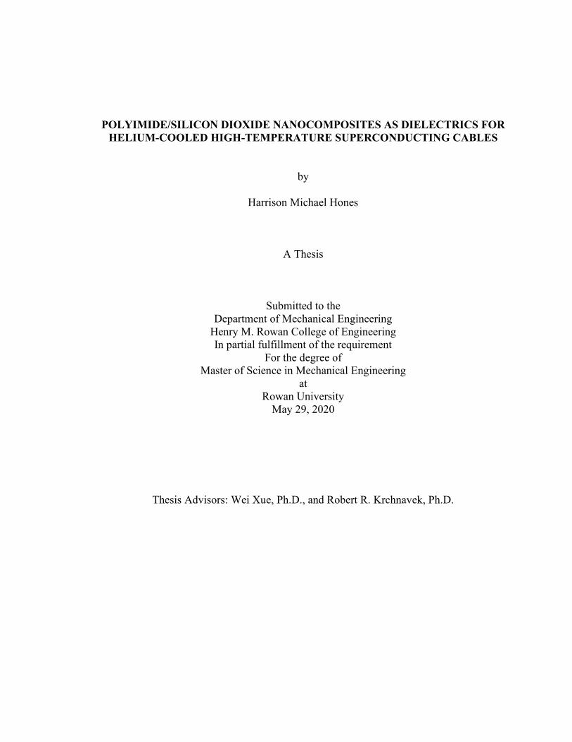
Abstract
Harrison Michael Hones POLYIMIDE/SILICON DIOXIDE NANOCOMPOSITES AS DIELECTRICS FOR
HELIUM-COOLED HIGH-TEMPERATURE SUPERCONDUCTING CABLES 2019-2020
Wei Xue, Ph.D., and Robert R. Krchnavek, Ph.D. Master of Science in Mechanical Engineering
In this thesis, polyimide (PI) and silicon dioxide (SiO2) were combined in the
form of a nanocomposite for use as a dielectric on helium-cooled high-temperature
superconducting (HTS) cables. Further, a cryogenic chamber was designed with the
intent of cooling samples to 40 K for dielectric and thermal contraction testing.
Composites were created through an in situ process which resulted in nanoparticle
formation within the host matrix. Samples were tested for dielectric strength at room
temperature (300 K) as well as cryogenic temperature (92 K) using liquid nitrogen as the
coolant. Composite samples tested at 300 K averaged a dielectric strength of about 175
kV/mm, while those tested cryogenically exhibited an average strength of around 275
kV/mm. Samples were imaged via scanning electron microscopy (SEM) both before and
after dielectric testing. Imaging samples broken down at 92 K revealed evidence of
electrical treeing, a breakdown mechanism discussed in this thesis. Finally, the helium
chamber has been designed to accommodate multiple testing systems at cryogenic
temperatures. Although this research is ongoing, the PI/SiO2 composite is already a
promising candidate as a cryogenic HTS cable dielectric.
vi
Table of Contents
Abstract ................................................................................................................................v
List of Figures .................................................................................................................... ix
List of Tables .................................................................................................................... xii
Chapter 1: Introduction ........................................................................................................1
1.1. Naval Ships and HTS Cables .................................................................................. 1
1.2. HTS Cable Applications ......................................................................................... 2
1.3. Dielectric Requirements.......................................................................................... 4
1.4. Nanocomposites ...................................................................................................... 7
1.4.1 Host Matrix – Polyimide ................................................................................. 8
1.4.2 Nanoparticle – Silicon Dioxide ....................................................................... 9
1.5. Cryogenic Testing Chamber ................................................................................. 10
1.6. Motivation and Objectives .................................................................................... 12
1.7. General Layout of Thesis ...................................................................................... 12
Chapter 2: Nanocomposite Fabrication .............................................................................14
2.1. Nanoparticle Distribution...................................................................................... 14
2.1.1. Ex Situ Method ............................................................................................. 15
2.1.2. In Situ Method .............................................................................................. 15
2.2. Thin Film Preparation ........................................................................................... 18
2.3. Discussion of Fabrication Methods ...................................................................... 20
Table of Contents (Continued)
vii
Chapter 3: Material Characterization .................................................................................23
3.1. Dielectric Breakdown Testing .............................................................................. 23
3.1.1. Dielectric Testing at Room Temperature ..................................................... 25
3.1.2. Dielectric Testing at Cryogenic Temperature .............................................. 27
3.2. Scanning Electron Microscopy ............................................................................. 30
3.2.1. Energy-Dispersive X-Ray Spectroscopy ...................................................... 31
Chapter 4: Characterization Results...................................................................................32
4.1. Dielectric Strength ................................................................................................ 32
4.2. SEM Imaging ........................................................................................................ 34
4.2.1. EDS Imaging ................................................................................................ 36
4.3. Breakdown Point Imaging .................................................................................... 37
4.4. Evidence of Treeing in Broken Down Samples .................................................... 41
Chapter 5: Cryogenic Testing Chamber ............................................................................43
5.1. Design Considerations .......................................................................................... 43
5.2. Inner Chamber Design .......................................................................................... 47
5.3. Outer Chamber Design ......................................................................................... 50
5.4. Chamber Simulations ............................................................................................ 52
Chapter 6: Conclusions and Future Works ........................................................................55

Table of Contents (Continued)
viii
6.1. Summary ............................................................................................................... 55
6.2. Future Works ........................................................................................................ 57
References ..........................................................................................................................61
ix
List of Figures
Figure Page
Figure 1. Three phase superconducting cable, with each phase separated by a dielectric, contained within a cryostat [5]. ........................................................................... 2
Figure 2. Layout of HTS cables along the hull of a Navy ship. HTS cables are indicated by grey lines running vertically and horizontally [12]. ....................................... 3
Figure 3. Schematic view of the HTS cable system installed in the Albany Project. The HTS cable runs underground to connect two termination boxes [17]. ................ 4
Figure 4. Schematic of helium atoms permeating layers of lapped dielectric tape. ........... 5
Figure 5. Contraction rates of common cryogenic materials, notably HTS cable cores and polymers [24]. ..................................................................................................... 6
Figure 6. An example of how a dielectric layer with a large CTE could fail when coated on an HTS cable with a lower CTE. .................................................................... 7
Figure 7. Schematic of a nanocomposite. The host matrix is depicted in yellow, while the nanoparticles are shown in grey. ......................................................................... 8
Figure 8. Chemical structure for PAA. The elements present are hydrogen, nitrogen, and oxygen [28]. ........................................................................................................ 9
Figure 9. Silica particles purchased from Sigma-Aldrich, 20 nm (left) and 80 nm (right) in diameter. ........................................................................................................ 10
Figure 10. Gaseous helium-cooled cryogenic chamber designed to cool a section of HTS cable [41]. .......................................................................................................... 11
Figure 11. Chemical structures of PAA and PI transitioning through the imidization process [42]. ...................................................................................................... 14
Figure 12. Simplified chemical reactions of the Stöber process resulting in the formation of silica and water. ............................................................................................ 17
Figure 13. From initial precursors, the steps of nanoparticle formation over time during the sol gel process [47]. ..................................................................................... 17
Figure 14. Silica nanoparticle introduction to PAA through (a) ex situ process, and (b) in situ process. ....................................................................................................... 18
List of Figures (Continued)
x
Figure Page
Figure 15. Profiles of two spin coating processes measuring speed over time (top), and resulting thickness of the films produced with each method (bottom). ............ 19
Figure 16. Temperature profile of the curing process over time. ..................................... 20
Figure 17. Two finished PI/SiO2 samples, created through ex situ process (left), and in situ process (right). ............................................................................................ 21
Figure 18. Optical profiles of two samples. Ex situ (top) has a peak to peak range of 2200 nm. In situ (bottom) has a peak to peak range of 400 nm. ................................ 22
Figure 19. Avalanche process showing how one accelerated electron (red) can result in many by ionizing atoms (blue). ......................................................................... 24
Figure 20. Schematic of treeing theory as a means of dielectric breakdown. .................. 25
Figure 21. Room temperature dielectric testing rig connected to the hipot tester. ........... 27
Figure 22. (a) Schematic of the cryogenic dielectric testing setup, with a zoomed-in view of a PI/SiO2 sample between two electrodes, and (b) an image of the electrode holders in the mount. ......................................................................................... 29
Figure 23. SEM image of the surface of a PA/SiO2 composite sample. Silica particles can be seen as dark grey circular masses, with the PA host represented by the lighter grey area. ................................................................................................ 31
Figure 24. Comparison of dielectric strength of 0-6% PI/SiO2 composites at 300 K (patterned red) and 92 K (solid blue). ............................................................... 33
Figure 25. SEM image of a PA/SiO2 composite sample containing 4% wt. silica. .......... 35
Figure 26. Number of particles within set diameter ranges. Data gathered from an SEM image of a 6% silica sample. ............................................................................. 36
Figure 27. Elemental map of silicon in a 5% wt. PA/SiO2 composite sample obtained through SEM-EDS. ........................................................................................... 37
Figure 28. SEM image of a breakdown point within a 2% PI/SiO2 composite sample broken down at 300 K. ...................................................................................... 39
List of Figures (Continued)
xi
Figure Page
Figure 29. SEM image of a point of breakdown within a 1% PI/SiO2 composite sample, tested at 92 K. .................................................................................................... 40
Figure 30. Close inspection of the material damaged in a cryogenic dielectric test, using a zoomed-in view of the 1% PI/SiO2 sample in Figure 29. ................................. 42
Figure 31. Cryocooler set up (a) provided by the Applied Superconductivity team at the NWSCPD, and (b) as a schematic. .................................................................... 45
Figure 32. Paschen’s curve, which plots combined values of pressure and distance against breakdown voltage [63]. .................................................................................... 47
Figure 33. Flow chart of the helium chamber with a valve diagram. ............................... 49
Figure 34. SolidWorks rendering of the inner testing chamber, contained within the outer vacuum chamber. .............................................................................................. 50
Figure 35. SolidWorks rendering of (a) the helium chamber, and (b) the cross-section of both chambers. .................................................................................................. 51
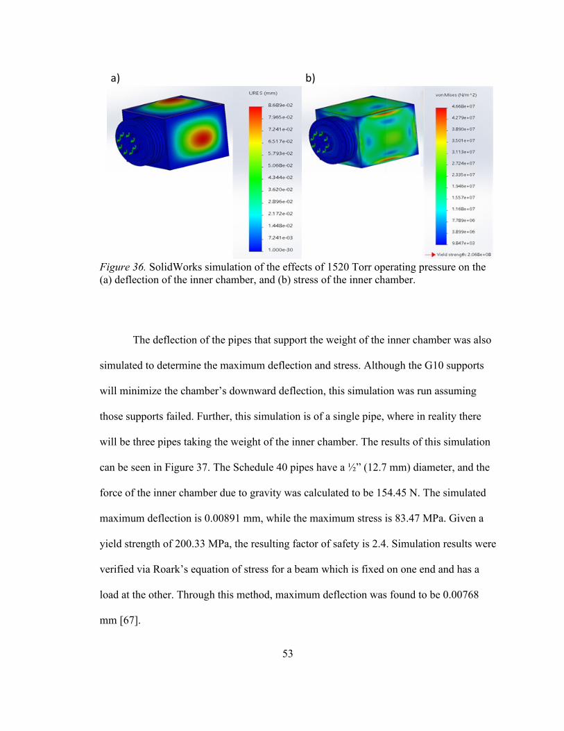
Figure 36. SolidWorks simulation of the effects of 1520 Torr operating pressure on the (a) deflection of the inner chamber, and (b) stress of the inner chamber. ......... 53
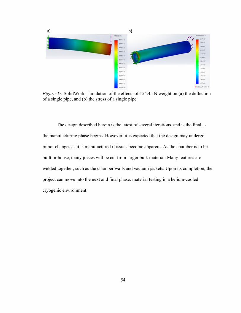
Figure 37. SolidWorks simulation of the effects of 154.45 N weight on (a) the deflection of a single pipe, and (b) the stress of a single pipe. ........................................... 54

xii
List of Tables
Table Page
Table 1. Equation used to determine mass of silica .......................................................... 15
Table 2. Equations used to determine mass of precursor materials .................................. 17
Table 3. Comparison of dielectric strength between this and other studies ..................... 57
1
Chapter 1
Introduction
1.1. Naval Ships and HTS Cables
Power generation and transmission are necessities for any technological device or
system, Navy ships included. Ships create a unique problem, however, in their
requirement to be self-sufficient for extended periods of time while at sea. Power must be
generated on board and transmitted to all subsystems on the ship, without the
infrastructure that is present for land-based systems, such as the overhead or underground
powerlines seen in cities and towns. One of the most critical limiting factors to onboard
power generation and transmission is the amount of space. Every square foot on a Navy
ship has a purpose, meaning a larger generator and larger cable bundles are not viable
solutions to an increase in power requirements. An increase in efficiency has the potential
to meet the ever increasing demand for electrical power on Navy ships.
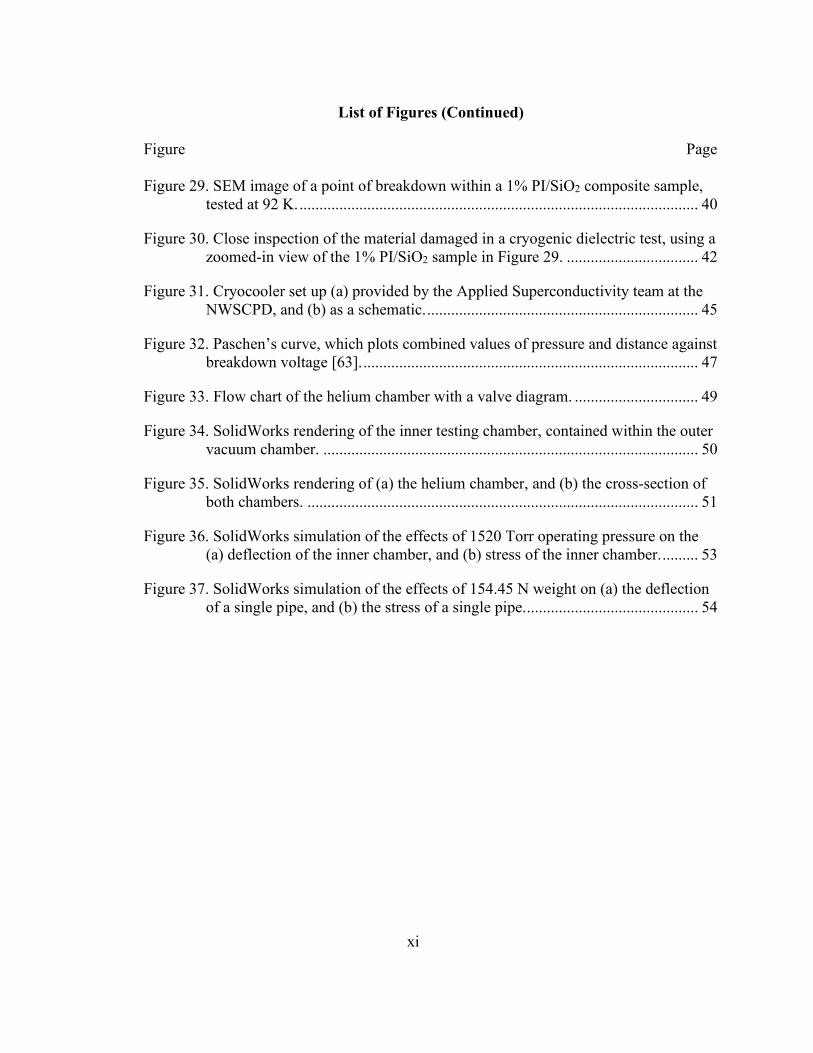
High-temperature superconducting (HTS) cables provide a means of increasing
power density by 200-800% from traditional cables [1]. HTS cables contain a core made
of a superconducting alloy, or a superconductor. When a superconductor is cooled to a
point below its transition temperature, its electrical resistance drops to zero, resulting in
100% power transmission efficiency [2, 3]. The cable core is usually a hollow cylinder,
but may be singular or in three phases [4]. In multi-phase cables, each phase is separated
by a dielectric layer. HTS cables are commonly cooled using liquid nitrogen (LN2) which
flows around the outer layer of the cable and through the hollow center. An example of a
three-phase HTS cable can be seen in Figure 1 [5].
2
Figure 1. Three phase superconducting cable, with each phase separated by a dielectric, contained within a cryostat [5].
1.2. HTS Cable Applications
HTS cables have a number of potential applications, one of which is a means to
increase power transmission on Navy ships while saving space and weight [6]. The
increased efficiency associated with these cables can be used on smaller systems, or on a
system requiring large amounts of electrical current such as a kinetic energy weapon,
commonly known as a rail gun. A rail gun may require as much as 3.4 MA to operate, a
current which would require many conventional cables [7, 8]. HTS cables have the
potential to transmit the same amount of current more efficiently while using less space.
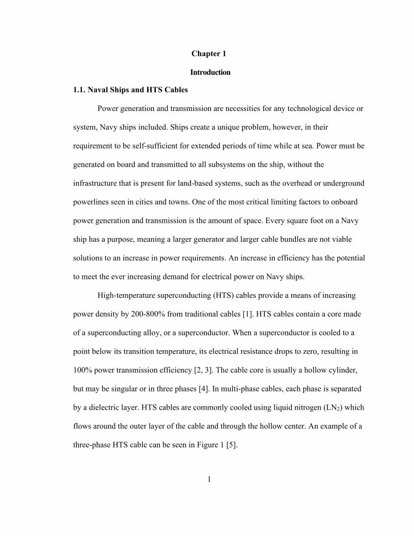
Navy ships develop a magnetic signature as they travel throughout Earth’s
magnetic field, a signature that can be picked up by other ships or mines with magnetic
triggers [9]. Rather than preventing this magnetic signature from developing, efforts have
been made to reduce the signature on ships through degaussing [10, 11]. The process of
3
degaussing requires the installation of a system of electrical cables along the hull of the
ship on both sides, which can be seen in Figure 2 [12]. Running the proper current
through these cables results in a magnetic field that cancels out the field output by the
ship [13]. Studies have shown that degaussing through HTS cables is not only feasible,
but beneficial in terms of weight, size, and cost [12, 14].
Figure 2. Layout of HTS cables along the hull of a Navy ship. HTS cables are indicated by grey lines running vertically and horizontally [12].
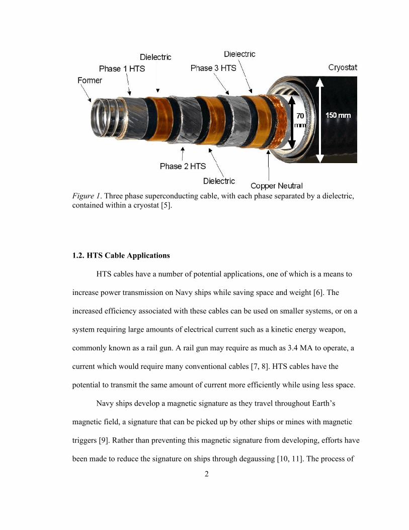
Superconducting cables are also a topic of interest in the electric power industry,
as the United States power grid is estimated to lose 10% of all electricity to inefficiencies
between the source and the customer [15]. Some HTS cable systems have been in place
since as early as 2006. In Albany, New York, a 350 m underground HTS cable was
installed within the power grid in one phase of the Albany Cable Project [16]. The cable
operated successfully and provided power to over 25,000 homes within its first year, and
is still operational [1, 17]. The schematic view of the cable system can be seen in Figure
3 [17]. Systems have also been installed in Asia and Europe, such as in the AmpaCity
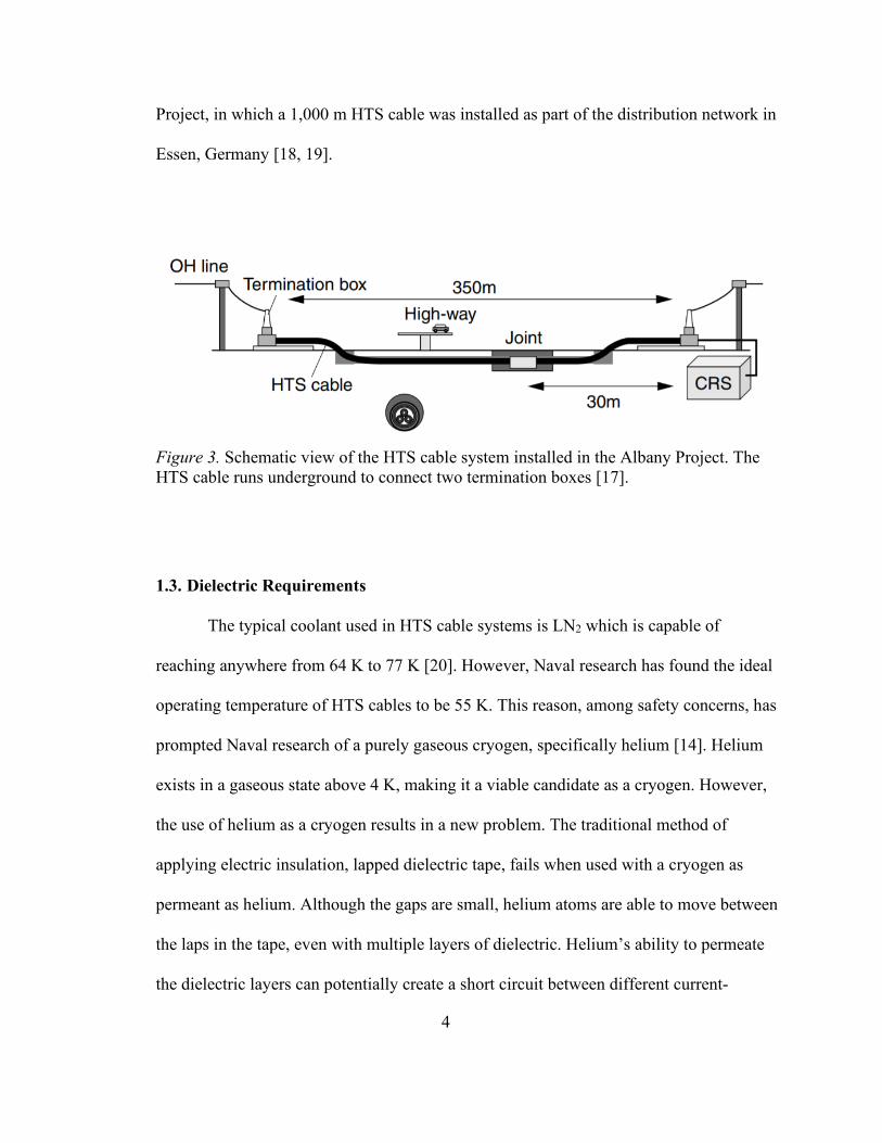
4
Project, in which a 1,000 m HTS cable was installed as part of the distribution network in
Essen, Germany [18, 19].
Figure 3. Schematic view of the HTS cable system installed in the Albany Project. The HTS cable runs underground to connect two termination boxes [17].
1.3. Dielectric Requirements
The typical coolant used in HTS cable systems is LN2 which is capable of
reaching anywhere from 64 K to 77 K [20]. However, Naval research has found the ideal
operating temperature of HTS cables to be 55 K. This reason, among safety concerns, has
prompted Naval research of a purely gaseous cryogen, specifically helium [14]. Helium
exists in a gaseous state above 4 K, making it a viable candidate as a cryogen. However,
the use of helium as a cryogen results in a new problem. The traditional method of
applying electric insulation, lapped dielectric tape, fails when used with a cryogen as
permeant as helium. Although the gaps are small, helium atoms are able to move between
the laps in the tape, even with multiple layers of dielectric. Helium’s ability to permeate
the dielectric layers can potentially create a short circuit between different current-
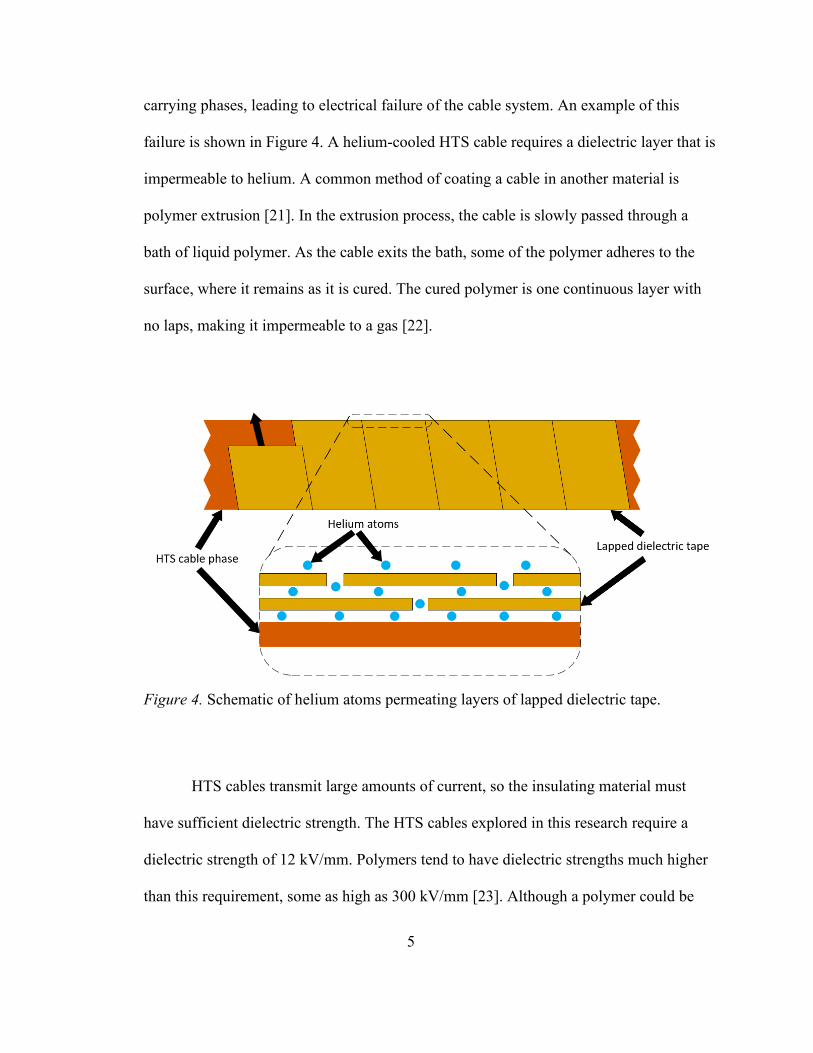
5
carrying phases, leading to electrical failure of the cable system. An example of this
failure is shown in Figure 4. A helium-cooled HTS cable requires a dielectric layer that is
impermeable to helium. A common method of coating a cable in another material is
polymer extrusion [21]. In the extrusion process, the cable is slowly passed through a
bath of liquid polymer. As the cable exits the bath, some of the polymer adheres to the
surface, where it remains as it is cured. The cured polymer is one continuous layer with
no laps, making it impermeable to a gas [22].
Figure 4. Schematic of helium atoms permeating layers of lapped dielectric tape.
HTS cables transmit large amounts of current, so the insulating material must
have sufficient dielectric strength. The HTS cables explored in this research require a
dielectric strength of 12 kV/mm. Polymers tend to have dielectric strengths much higher
than this requirement, some as high as 300 kV/mm [23]. Although a polymer could be
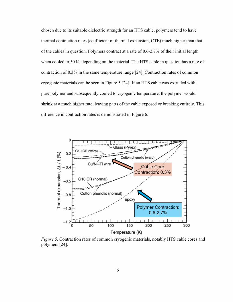
6
chosen due to its suitable dielectric strength for an HTS cable, polymers tend to have
thermal contraction rates (coefficient of thermal expansion, CTE) much higher than that
of the cables in question. Polymers contract at a rate of 0.6-2.7% of their initial length
when cooled to 50 K, depending on the material. The HTS cable in question has a rate of
contraction of 0.3% in the same temperature range [24]. Contraction rates of common
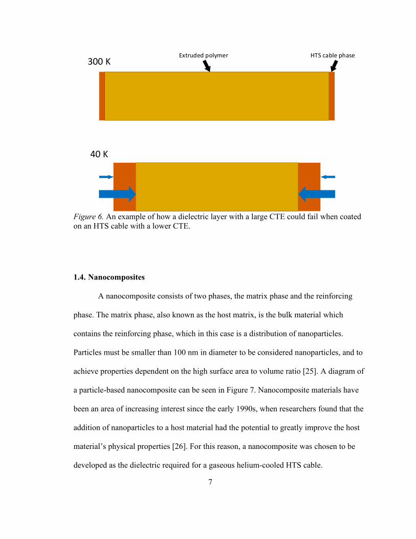
cryogenic materials can be seen in Figure 5 [24]. If an HTS cable was extruded with a
pure polymer and subsequently cooled to cryogenic temperature, the polymer would
shrink at a much higher rate, leaving parts of the cable exposed or breaking entirely. This
difference in contraction rates is demonstrated in Figure 6.
Figure 5. Contraction rates of common cryogenic materials, notably HTS cable cores and polymers [24].
7
Figure 6. An example of how a dielectric layer with a large CTE could fail when coated on an HTS cable with a lower CTE.
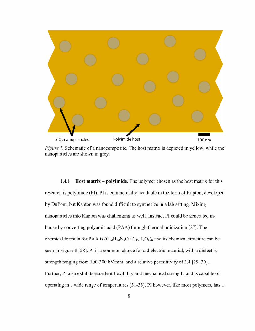
1.4. Nanocomposites
A nanocomposite consists of two phases, the matrix phase and the reinforcing
phase. The matrix phase, also known as the host matrix, is the bulk material which
contains the reinforcing phase, which in this case is a distribution of nanoparticles.
Particles must be smaller than 100 nm in diameter to be considered nanoparticles, and to
achieve properties dependent on the high surface area to volume ratio [25]. A diagram of
a particle-based nanocomposite can be seen in Figure 7. Nanocomposite materials have
been an area of increasing interest since the early 1990s, when researchers found that the
addition of nanoparticles to a host material had the potential to greatly improve the host
material’s physical properties [26]. For this reason, a nanocomposite was chosen to be
developed as the dielectric required for a gaseous helium-cooled HTS cable.
HTS cable phaseExtruded polymer300 K
40 K
8
Figure 7. Schematic of a nanocomposite. The host matrix is depicted in yellow, while the nanoparticles are shown in grey.
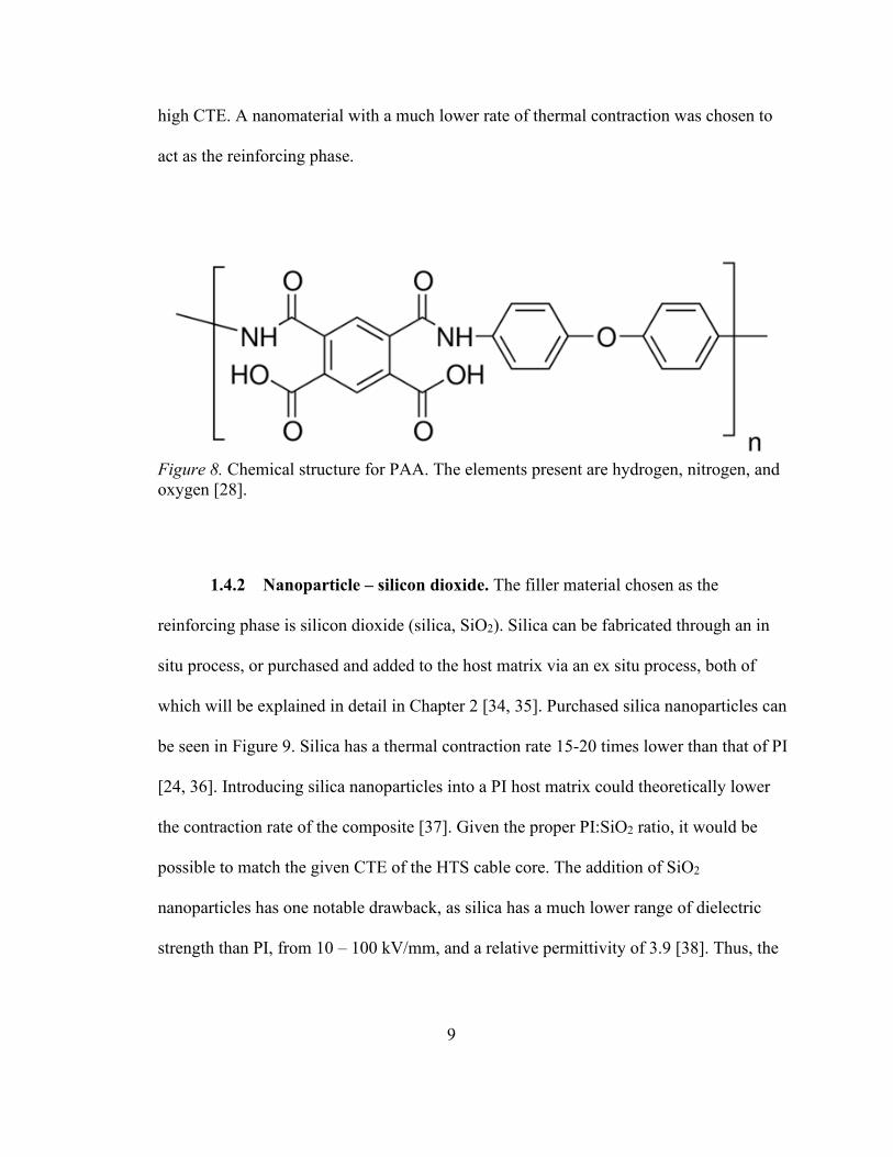
1.4.1 Host matrix – polyimide. The polymer chosen as the host matrix for this
research is polyimide (PI). PI is commercially available in the form of Kapton, developed
by DuPont, but Kapton was found difficult to synthesize in a lab setting. Mixing
nanoparticles into Kapton was challenging as well. Instead, PI could be generated in-
house by converting polyamic acid (PAA) through thermal imidization [27]. The
chemical formula for PAA is (C12H12N2O ‧ C10H2O6)n and its chemical structure can be
seen in Figure 8 [28]. PI is a common choice for a dielectric material, with a dielectric
strength ranging from 100-300 kV/mm, and a relative permittivity of 3.4 [29, 30].
Further, PI also exhibits excellent flexibility and mechanical strength, and is capable of
operating in a wide range of temperatures [31-33]. PI however, like most polymers, has a
SiO2 nanoparticles Polyimide host 100 nm
9
high CTE. A nanomaterial with a much lower rate of thermal contraction was chosen to
act as the reinforcing phase.
Figure 8. Chemical structure for PAA. The elements present are hydrogen, nitrogen, and oxygen [28].
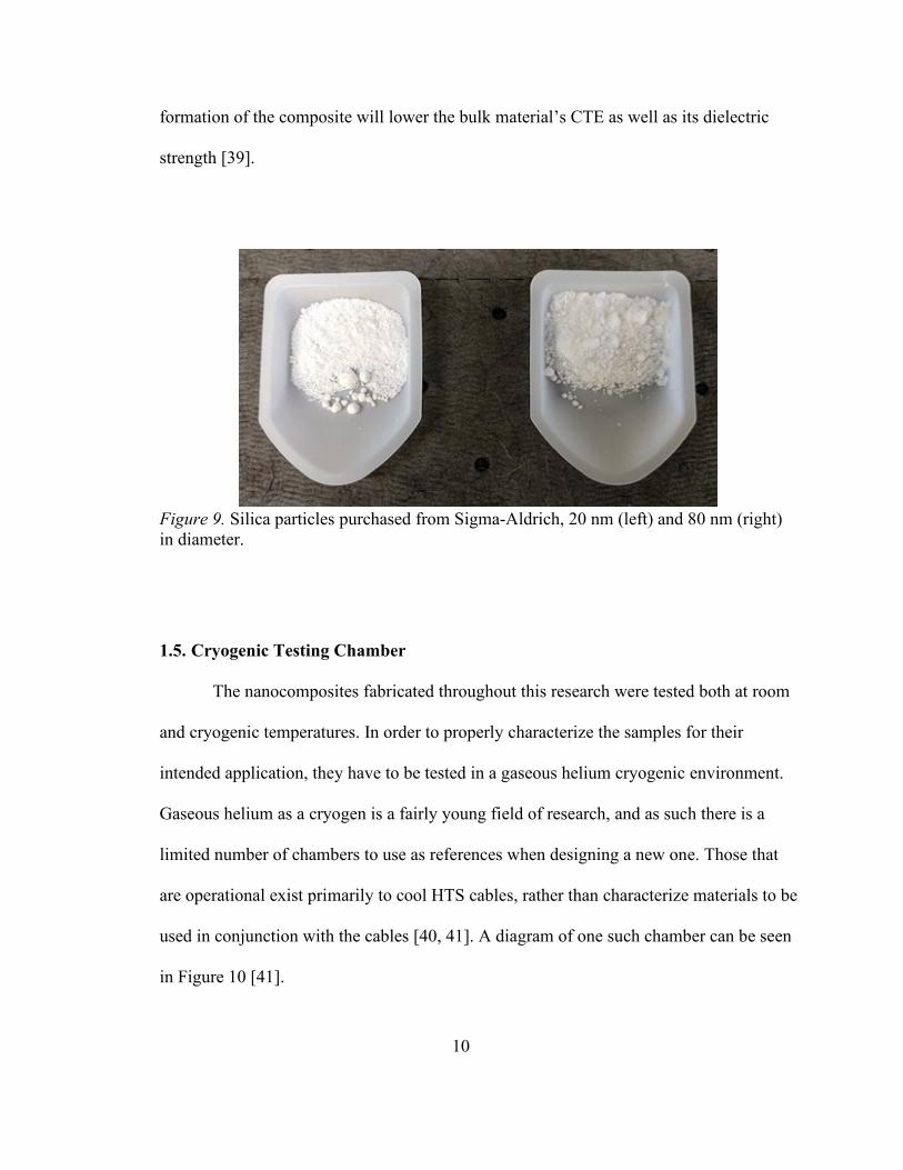
1.4.2 Nanoparticle – silicon dioxide. The filler material chosen as the
reinforcing phase is silicon dioxide (silica, SiO2). Silica can be fabricated through an in
situ process, or purchased and added to the host matrix via an ex situ process, both of
which will be explained in detail in Chapter 2 [34, 35]. Purchased silica nanoparticles can
be seen in Figure 9. Silica has a thermal contraction rate 15-20 times lower than that of PI
[24, 36]. Introducing silica nanoparticles into a PI host matrix could theoretically lower
the contraction rate of the composite [37]. Given the proper PI:SiO2 ratio, it would be
possible to match the given CTE of the HTS cable core. The addition of SiO2
nanoparticles has one notable drawback, as silica has a much lower range of dielectric
strength than PI, from 10 – 100 kV/mm, and a relative permittivity of 3.9 [38]. Thus, the
10
formation of the composite will lower the bulk material’s CTE as well as its dielectric
strength [39].
Figure 9. Silica particles purchased from Sigma-Aldrich, 20 nm (left) and 80 nm (right) in diameter.
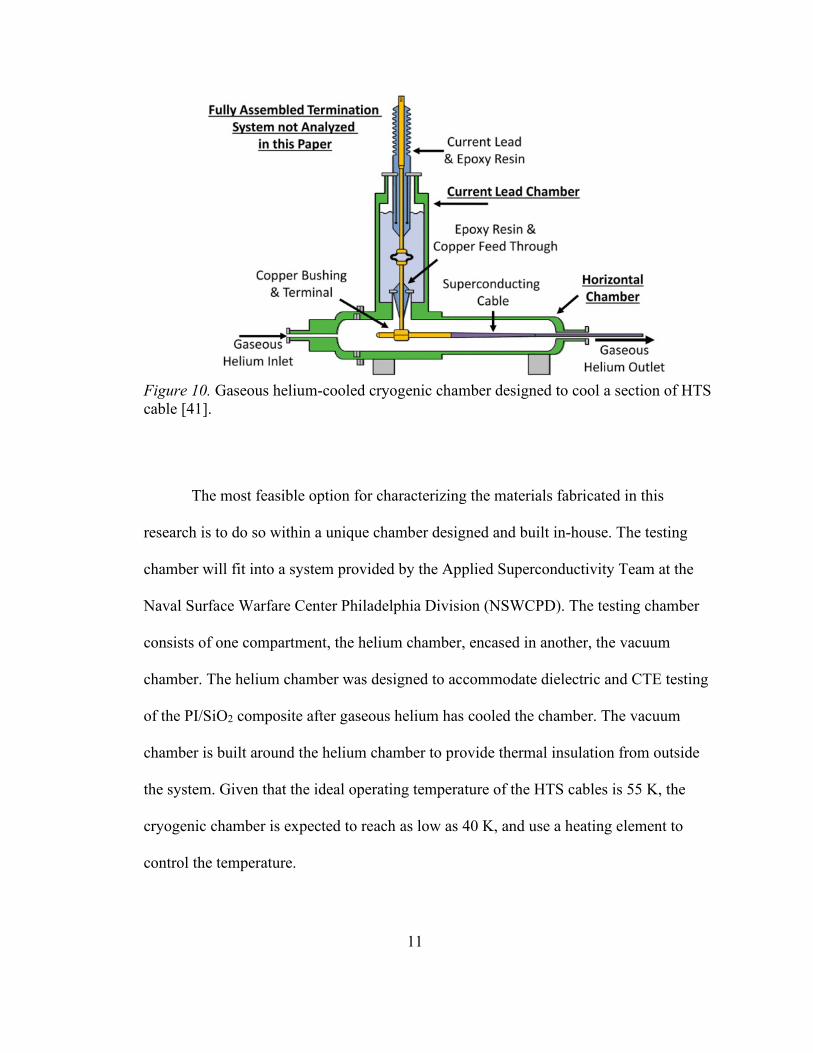
1.5. Cryogenic Testing Chamber
The nanocomposites fabricated throughout this research were tested both at room
and cryogenic temperatures. In order to properly characterize the samples for their
intended application, they have to be tested in a gaseous helium cryogenic environment.
Gaseous helium as a cryogen is a fairly young field of research, and as such there is a
limited number of chambers to use as references when designing a new one. Those that
are operational exist primarily to cool HTS cables, rather than characterize materials to be
used in conjunction with the cables [40, 41]. A diagram of one such chamber can be seen
in Figure 10 [41].
11
Figure 10. Gaseous helium-cooled cryogenic chamber designed to cool a section of HTS cable [41].
The most feasible option for characterizing the materials fabricated in this
research is to do so within a unique chamber designed and built in-house. The testing
chamber will fit into a system provided by the Applied Superconductivity Team at the
Naval Surface Warfare Center Philadelphia Division (NSWCPD). The testing chamber
consists of one compartment, the helium chamber, encased in another, the vacuum
chamber. The helium chamber was designed to accommodate dielectric and CTE testing
of the PI/SiO2 composite after gaseous helium has cooled the chamber. The vacuum
chamber is built around the helium chamber to provide thermal insulation from outside
the system. Given that the ideal operating temperature of the HTS cables is 55 K, the
cryogenic chamber is expected to reach as low as 40 K, and use a heating element to
control the temperature.
12
1.6. Motivation and Objectives
In this research the relationship between temperature and physical properties of a
polymer nanocomposite are studied, with the hope of creating a dielectric material
suitable for use on helium-cooled HTS cables. The properties of the composite can be
adjusted due to the rule of mixtures, which uses the concentration of a composite to
estimate material properties. HTS cables have been used in recent years, although they
used LN2 as a coolant. In an effort to make these HTS cables even more efficient, a few
research groups have explored this topic, but most of the research done here is unique and
unprecedented. The motivation of this research is two-fold: to create the dielectric
material from a PI/SiO2 nanocomposite, and to design and fabricate the testing chamber
necessary to characterize the composite in a helium-cooled cryogenic environment.
The objectives of this research include:
1. Create a well-dispersed PI/SiO2 nanocomposite.
2. Perform dielectric tests on composites with varying SiO2 concentrations to
determine which concentrations result in viable candidates for HTS
dielectrics.
3. Measure the relationship between temperature and dielectric strength.
4. Design a helium-cooled cryogenic chamber to perform dielectric and CTE
tests.
1.7. General Layout of Thesis
In Chapter 2 of this thesis, the two methods used to generate silica nanoparticles
are described, as well as the fabrication method of the thin film samples. The quality and
13
consistency of the two particle generation methods are discussed. The means through
which the samples were characterized are described in Chapter 3, including dielectric
testing and scanning electron microscopy. The methods for dielectric testing at room and
cryogenic temperature are depicted. Chapter 4 contains the results from these tests, in the
form of dielectric strength values and SEM images of the samples before and after
breakdown. These SEM images are also used in the discussion of the dielectric
breakdown theory known as electrical treeing. The design of the helium chamber is
detailed in Chapter 5, along with the safety considerations and simulations run on the
latest iteration of this design. The paper is concluded in Chapter 6, which contains a
summary of all work completed to this point, as well as the future works and goals of this
research as it continues into the future.
14
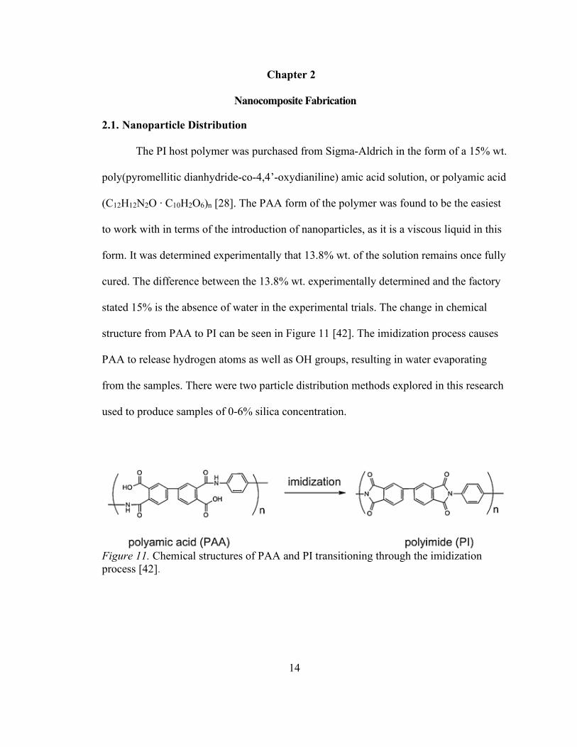
Chapter 2
Nanocomposite Fabrication
2.1. Nanoparticle Distribution
The PI host polymer was purchased from Sigma-Aldrich in the form of a 15% wt.
poly(pyromellitic dianhydride-co-4,4’-oxydianiline) amic acid solution, or polyamic acid
(C12H12N2O ‧ C10H2O6)n [28]. The PAA form of the polymer was found to be the easiest
to work with in terms of the introduction of nanoparticles, as it is a viscous liquid in this
form. It was determined experimentally that 13.8% wt. of the solution remains once fully
cured. The difference between the 13.8% wt. experimentally determined and the factory
stated 15% is the absence of water in the experimental trials. The change in chemical
structure from PAA to PI can be seen in Figure 11 [42]. The imidization process causes
PAA to release hydrogen atoms as well as OH groups, resulting in water evaporating
from the samples. There were two particle distribution methods explored in this research
used to produce samples of 0-6% silica concentration.
Figure 11. Chemical structures of PAA and PI transitioning through the imidization process [42].
15
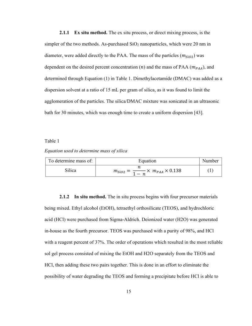
2.1.1 Ex situ method. The ex situ process, or direct mixing process, is the
simpler of the two methods. As-purchased SiO2 nanoparticles, which were 20 nm in
diameter, were added directly to the PAA. The mass of the particles (𝑚𝑚𝑆𝑆𝑆𝑆𝑆𝑆2) was
dependent on the desired percent concentration (𝑛𝑛) and the mass of PAA (𝑚𝑚𝑃𝑃𝑃𝑃𝑃𝑃), and
determined through Equation (1) in Table 1. Dimethylacetamide (DMAC) was added as a
dispersion solvent at a ratio of 15 mL per gram of silica, as it was found to limit the
agglomeration of the particles. The silica/DMAC mixture was sonicated in an ultrasonic
bath for 30 minutes, which was enough time to create a uniform dispersion [43].
Table 1
Equation used to determine mass of silica
To determine mass of: Equation Number
Silica 𝑚𝑚𝑆𝑆𝑆𝑆𝑆𝑆2 = 𝑛𝑛
1 − 𝑛𝑛× 𝑚𝑚𝑃𝑃𝑃𝑃𝑃𝑃 × 0.138
(1)
2.1.2 In situ method. The in situ process begins with four precursor materials
being mixed. Ethyl alcohol (EtOH), tetraethyl orthosilicate (TEOS), and hydrochloric
acid (HCl) were purchased from Sigma-Aldrich. Deionized water (H2O) was generated
in-house as the fourth precursor. TEOS was purchased with a purity of 98%, and HCl
with a reagent percent of 37%. The order of operations which resulted in the most reliable
sol gel process consisted of mixing the EtOH and H2O separately from the TEOS and
HCl, then adding these two pairs together. This is done in an effort to eliminate the
possibility of water degrading the TEOS and forming a precipitate before HCl is able to
16
catalyze the sol gel process. Further, adding the TEOS and HCl to the EtOH and H2O
prevents the acid from possibly splashing back, if water was added to the acid.
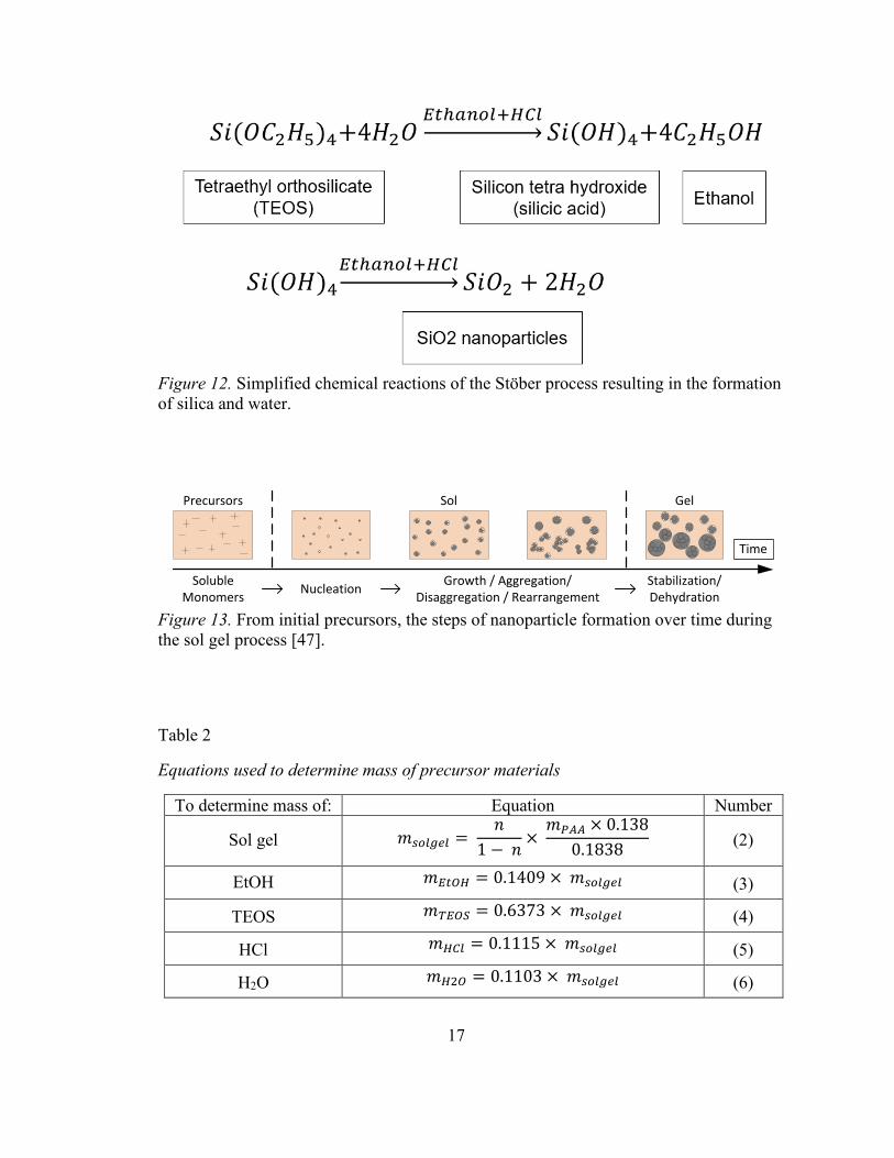
The four precursor materials were set to mix at 350 rpm for 30 minutes, during
which time the silica nanoparticles would form through a sol gel process known as the
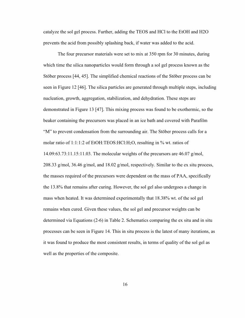
Stöber process [44, 45]. The simplified chemical reactions of the Stöber process can be
seen in Figure 12 [46]. The silica particles are generated through multiple steps, including
nucleation, growth, aggregation, stabilization, and dehydration. These steps are
demonstrated in Figure 13 [47]. This mixing process was found to be exothermic, so the
beaker containing the precursors was placed in an ice bath and covered with Parafilm
“M” to prevent condensation from the surrounding air. The Stöber process calls for a
molar ratio of 1:1:1:2 of EtOH:TEOS:HCl:H2O, resulting in % wt. ratios of
14.09:63.73:11.15:11.03. The molecular weights of the precursors are 46.07 g/mol,
208.33 g/mol, 36.46 g/mol, and 18.02 g/mol, respectively. Similar to the ex situ process,
the masses required of the precursors were dependent on the mass of PAA, specifically
the 13.8% that remains after curing. However, the sol gel also undergoes a change in
mass when heated. It was determined experimentally that 18.38% wt. of the sol gel
remains when cured. Given these values, the sol gel and precursor weights can be
determined via Equations (2-6) in Table 2. Schematics comparing the ex situ and in situ
processes can be seen in Figure 14. This in situ process is the latest of many iterations, as
it was found to produce the most consistent results, in terms of quality of the sol gel as
well as the properties of the composite.
17
Figure 12. Simplified chemical reactions of the Stöber process resulting in the formation of silica and water.
Figure 13. From initial precursors, the steps of nanoparticle formation over time during the sol gel process [47].
Table 2
Equations used to determine mass of precursor materials
To determine mass of: Equation Number
Sol gel 𝑚𝑚𝑠𝑠𝑠𝑠𝑠𝑠𝑠𝑠𝑠𝑠𝑠𝑠 = 𝑛𝑛
1 − 𝑛𝑛× 𝑚𝑚𝑃𝑃𝑃𝑃𝑃𝑃 × 0.138
0.1838
(2)
EtOH 𝑚𝑚𝐸𝐸𝐸𝐸𝑆𝑆𝐸𝐸 = 0.1409 × 𝑚𝑚𝑠𝑠𝑠𝑠𝑠𝑠𝑠𝑠𝑠𝑠𝑠𝑠
(3)
TEOS 𝑚𝑚𝑇𝑇𝐸𝐸𝑆𝑆𝑆𝑆 = 0.6373 × 𝑚𝑚𝑠𝑠𝑠𝑠𝑠𝑠𝑠𝑠𝑠𝑠𝑠𝑠
(4)
HCl 𝑚𝑚𝐸𝐸𝐻𝐻𝑠𝑠 = 0.1115 × 𝑚𝑚𝑠𝑠𝑠𝑠𝑠𝑠𝑠𝑠𝑠𝑠𝑠𝑠
(5)
H2O 𝑚𝑚𝐸𝐸2𝑆𝑆 = 0.1103 × 𝑚𝑚𝑠𝑠𝑠𝑠𝑠𝑠𝑠𝑠𝑠𝑠𝑠𝑠
(6)
Precursors Sol Gel
Nucleation Growth / Aggregation/ Disaggregation / Rearrangement
Stabilization/Dehydration
Time
Soluble Monomers
18
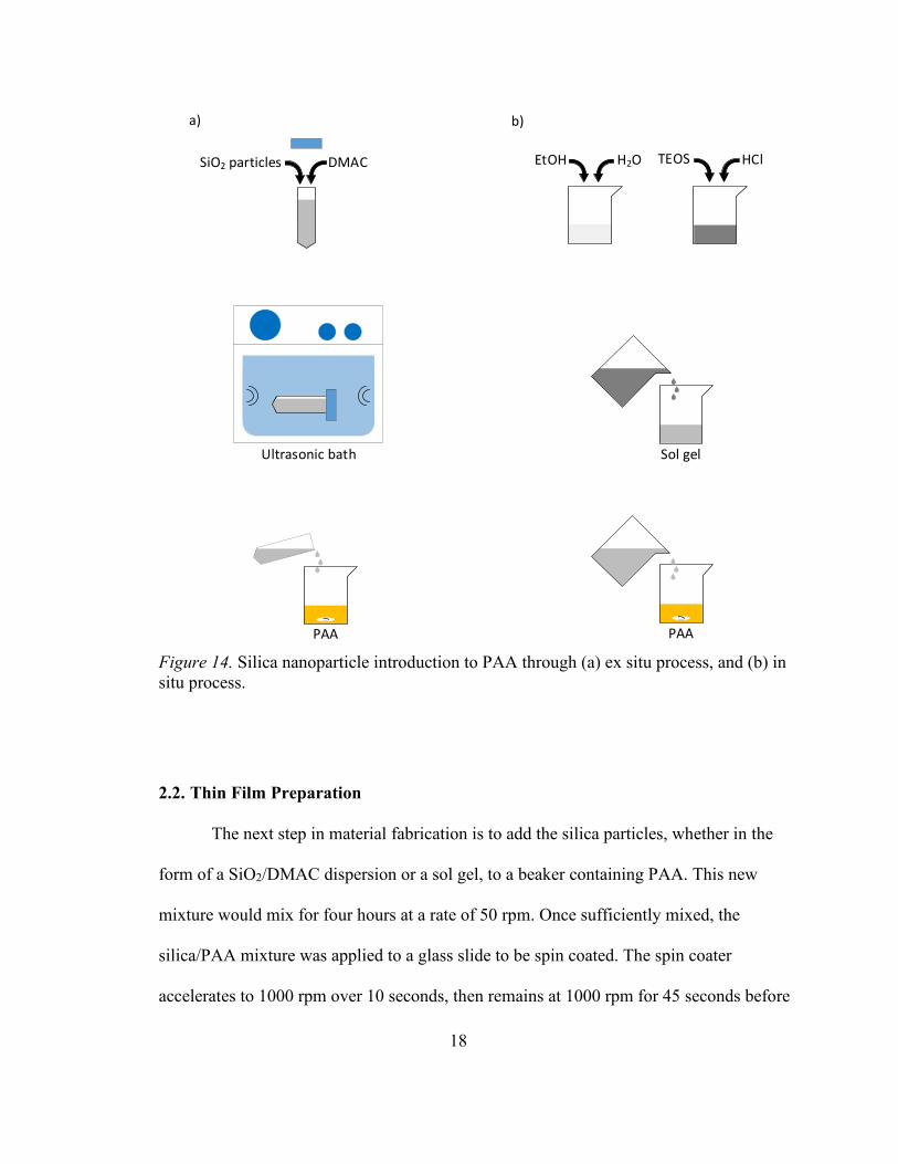
Figure 14. Silica nanoparticle introduction to PAA through (a) ex situ process, and (b) in situ process.
2.2. Thin Film Preparation
The next step in material fabrication is to add the silica particles, whether in the
form of a SiO2/DMAC dispersion or a sol gel, to a beaker containing PAA. This new
mixture would mix for four hours at a rate of 50 rpm. Once sufficiently mixed, the
silica/PAA mixture was applied to a glass slide to be spin coated. The spin coater
accelerates to 1000 rpm over 10 seconds, then remains at 1000 rpm for 45 seconds before
SiO2 particles DMAC
Ultrasonic bath
PAA PAA
Sol gel
a) b)
TEOS HClEtOH H2O
19
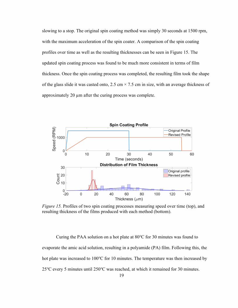
slowing to a stop. The original spin coating method was simply 30 seconds at 1500 rpm,
with the maximum acceleration of the spin coater. A comparison of the spin coating
profiles over time as well as the resulting thicknesses can be seen in Figure 15. The
updated spin coating process was found to be much more consistent in terms of film
thickness. Once the spin coating process was completed, the resulting film took the shape
of the glass slide it was casted onto, 2.5 cm × 7.5 cm in size, with an average thickness of
approximately 20 µm after the curing process was complete.
Figure 15. Profiles of two spin coating processes measuring speed over time (top), and resulting thickness of the films produced with each method (bottom).
Curing the PAA solution on a hot plate at 80℃ for 30 minutes was found to
evaporate the amic acid solution, resulting in a polyamide (PA) film. Following this, the
hot plate was increased to 100℃ for 10 minutes. The temperature was then increased by
25℃ every 5 minutes until 250℃ was reached, at which it remained for 30 minutes.
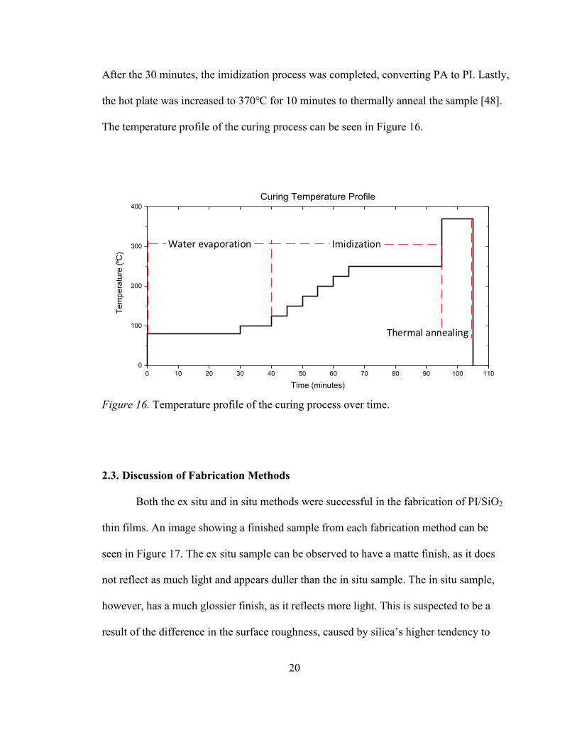
20
After the 30 minutes, the imidization process was completed, converting PA to PI. Lastly,
the hot plate was increased to 370℃ for 10 minutes to thermally anneal the sample [48].
The temperature profile of the curing process can be seen in Figure 16.
Figure 16. Temperature profile of the curing process over time.
2.3. Discussion of Fabrication Methods
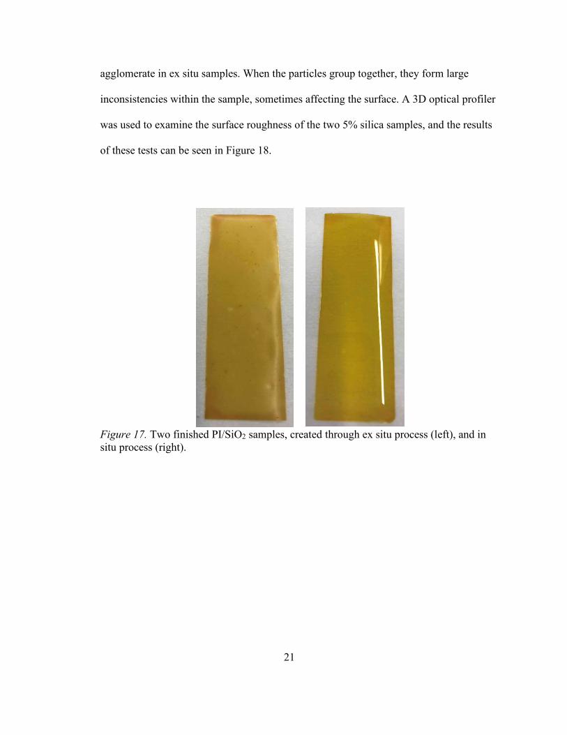
Both the ex situ and in situ methods were successful in the fabrication of PI/SiO2
thin films. An image showing a finished sample from each fabrication method can be
seen in Figure 17. The ex situ sample can be observed to have a matte finish, as it does
not reflect as much light and appears duller than the in situ sample. The in situ sample,
however, has a much glossier finish, as it reflects more light. This is suspected to be a
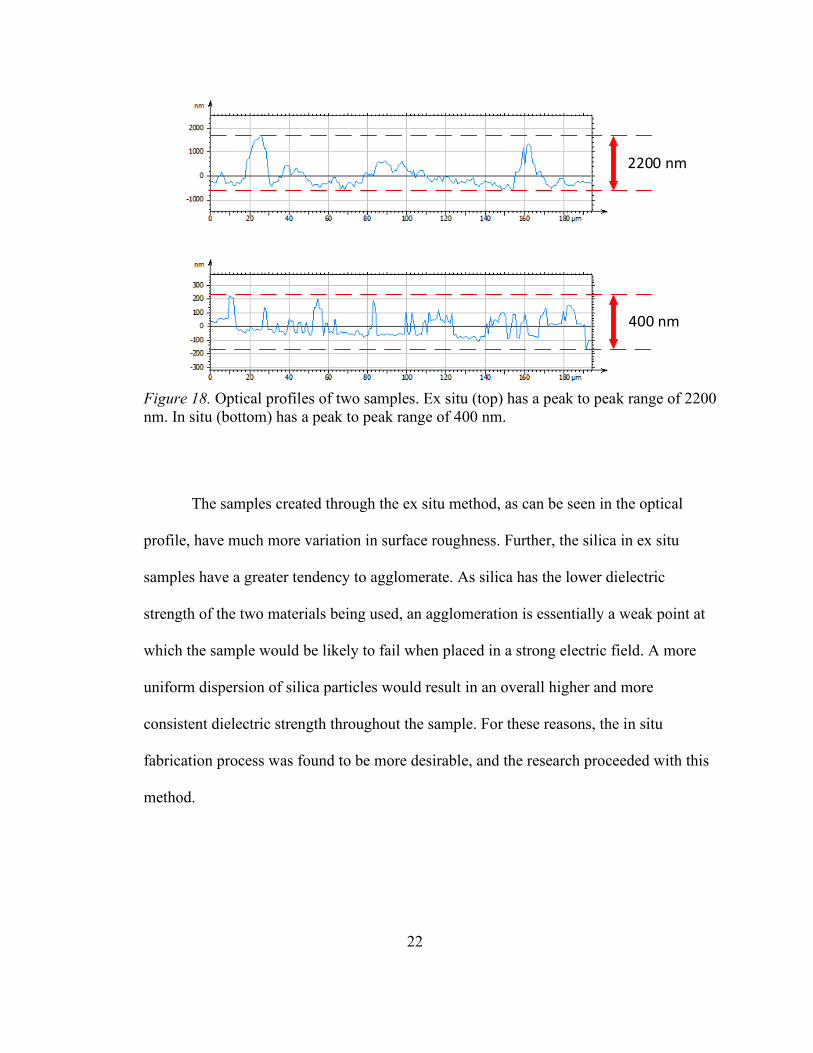
result of the difference in the surface roughness, caused by silica’s higher tendency to
0 10 20 30 40 50 60 70 80 90 100 1100
100
200
300
400Curing Temperature Profile
Tem
pera
ture
( C
)
Time (minutes)
Water evaporation Imidization
Thermal annealing
21
agglomerate in ex situ samples. When the particles group together, they form large
inconsistencies within the sample, sometimes affecting the surface. A 3D optical profiler
was used to examine the surface roughness of the two 5% silica samples, and the results
of these tests can be seen in Figure 18.
Figure 17. Two finished PI/SiO2 samples, created through ex situ process (left), and in situ process (right).
22
Figure 18. Optical profiles of two samples. Ex situ (top) has a peak to peak range of 2200 nm. In situ (bottom) has a peak to peak range of 400 nm.
The samples created through the ex situ method, as can be seen in the optical
profile, have much more variation in surface roughness. Further, the silica in ex situ
samples have a greater tendency to agglomerate. As silica has the lower dielectric
strength of the two materials being used, an agglomeration is essentially a weak point at
which the sample would be likely to fail when placed in a strong electric field. A more
uniform dispersion of silica particles would result in an overall higher and more
consistent dielectric strength throughout the sample. For these reasons, the in situ
fabrication process was found to be more desirable, and the research proceeded with this
method.
2200 nm
400 nm
23
Chapter 3
Material Characterization
3.1. Dielectric Breakdown Testing
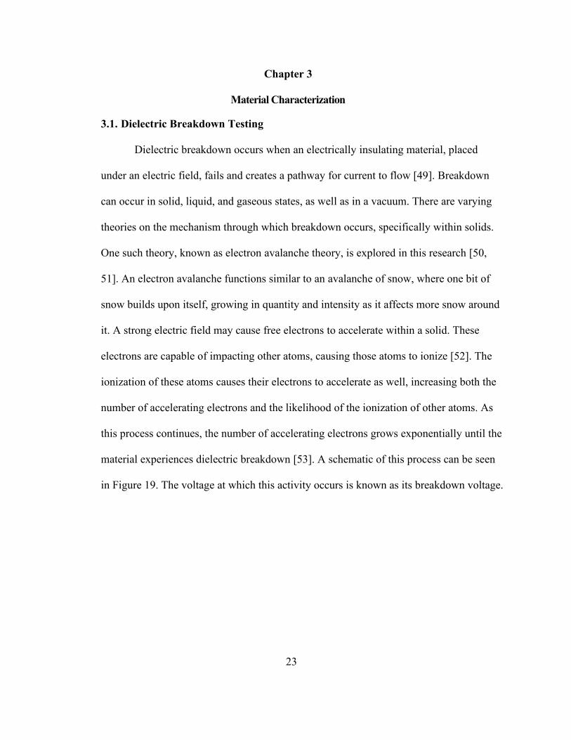
Dielectric breakdown occurs when an electrically insulating material, placed
under an electric field, fails and creates a pathway for current to flow [49]. Breakdown
can occur in solid, liquid, and gaseous states, as well as in a vacuum. There are varying
theories on the mechanism through which breakdown occurs, specifically within solids.
One such theory, known as electron avalanche theory, is explored in this research [50,
51]. An electron avalanche functions similar to an avalanche of snow, where one bit of
snow builds upon itself, growing in quantity and intensity as it affects more snow around
it. A strong electric field may cause free electrons to accelerate within a solid. These
electrons are capable of impacting other atoms, causing those atoms to ionize [52]. The
ionization of these atoms causes their electrons to accelerate as well, increasing both the
number of accelerating electrons and the likelihood of the ionization of other atoms. As
this process continues, the number of accelerating electrons grows exponentially until the
material experiences dielectric breakdown [53]. A schematic of this process can be seen
in Figure 19. The voltage at which this activity occurs is known as its breakdown voltage.
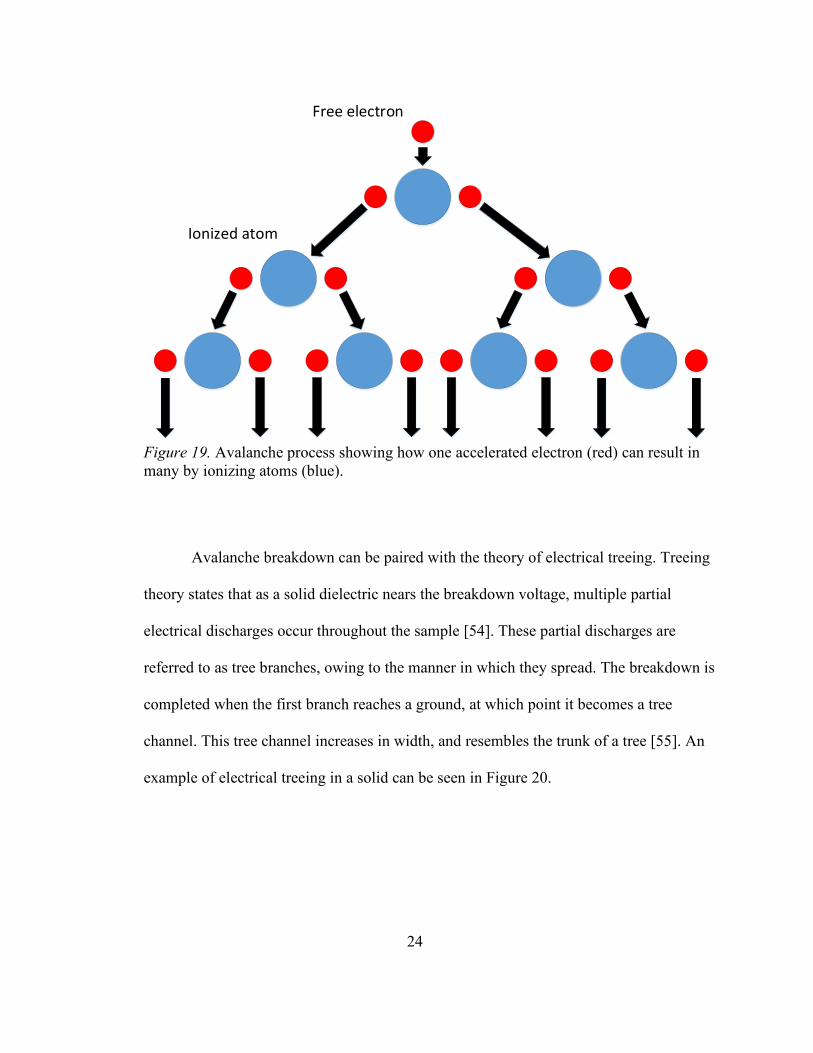
24
Figure 19. Avalanche process showing how one accelerated electron (red) can result in many by ionizing atoms (blue).
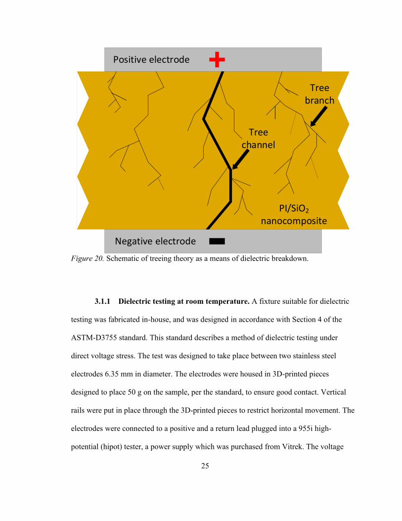
Avalanche breakdown can be paired with the theory of electrical treeing. Treeing
theory states that as a solid dielectric nears the breakdown voltage, multiple partial
electrical discharges occur throughout the sample [54]. These partial discharges are
referred to as tree branches, owing to the manner in which they spread. The breakdown is
completed when the first branch reaches a ground, at which point it becomes a tree
channel. This tree channel increases in width, and resembles the trunk of a tree [55]. An
example of electrical treeing in a solid can be seen in Figure 20.
Free electron
Ionized atom
25
Figure 20. Schematic of treeing theory as a means of dielectric breakdown.
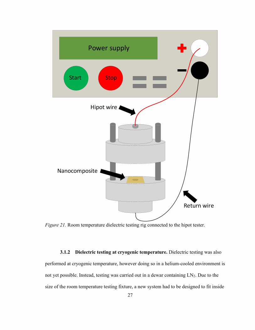
3.1.1 Dielectric testing at room temperature. A fixture suitable for dielectric
testing was fabricated in-house, and was designed in accordance with Section 4 of the
ASTM-D3755 standard. This standard describes a method of dielectric testing under
direct voltage stress. The test was designed to take place between two stainless steel
electrodes 6.35 mm in diameter. The electrodes were housed in 3D-printed pieces
designed to place 50 g on the sample, per the standard, to ensure good contact. Vertical
rails were put in place through the 3D-printed pieces to restrict horizontal movement. The
electrodes were connected to a positive and a return lead plugged into a 955i high-
potential (hipot) tester, a power supply which was purchased from Vitrek. The voltage
Tree channel
Tree branch
Positive electrode
Negative electrode
PI/SiO2 nanocomposite

26
applied across the sample increased at a rate of 500 V/s, until the sample was broken
down. Breakdown was detected by the hipot when a minimum of a 5 mA current reached
the electrode connected to the return wire, which caused the test to immediately stop.
Sample size could vary, but had a minimum of 1.5 cm × 1.5 cm to prevent the current
from sparking over. A schematic of the testing fixture connected to the hipot tester can be
seen in Figure 21.
27
Figure 21. Room temperature dielectric testing rig connected to the hipot tester.
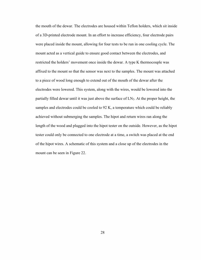
3.1.2 Dielectric testing at cryogenic temperature. Dielectric testing was also
performed at cryogenic temperature, however doing so in a helium-cooled environment is
not yet possible. Instead, testing was carried out in a dewar containing LN2. Due to the
size of the room temperature testing fixture, a new system had to be designed to fit inside
Power supply
StopStart
Hipot wire
Return wire
Nanocomposite
28
the mouth of the dewar. The electrodes are housed within Teflon holders, which sit inside
of a 3D-printed electrode mount. In an effort to increase efficiency, four electrode pairs
were placed inside the mount, allowing for four tests to be run in one cooling cycle. The
mount acted as a vertical guide to ensure good contact between the electrodes, and
restricted the holders’ movement once inside the dewar. A type K thermocouple was
affixed to the mount so that the sensor was next to the samples. The mount was attached
to a piece of wood long enough to extend out of the mouth of the dewar after the
electrodes were lowered. This system, along with the wires, would be lowered into the
partially filled dewar until it was just above the surface of LN2. At the proper height, the
samples and electrodes could be cooled to 92 K, a temperature which could be reliably
achieved without submerging the samples. The hipot and return wires ran along the
length of the wood and plugged into the hipot tester on the outside. However, as the hipot
tester could only be connected to one electrode at a time, a switch was placed at the end
of the hipot wires. A schematic of this system and a close up of the electrodes in the
mount can be seen in Figure 22.
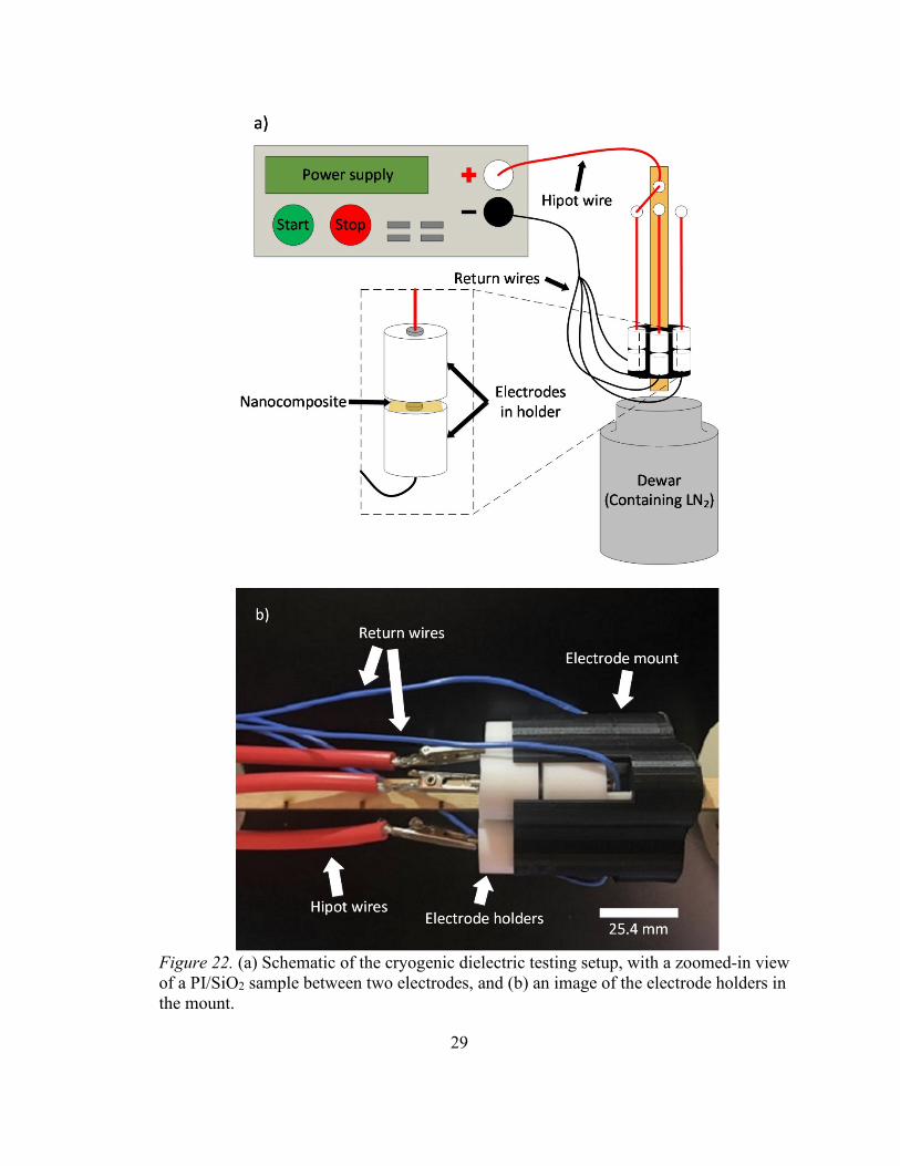
29
Figure 22. (a) Schematic of the cryogenic dielectric testing setup, with a zoomed-in view of a PI/SiO2 sample between two electrodes, and (b) an image of the electrode holders in the mount.
30
3.2. Scanning Electron Microscopy
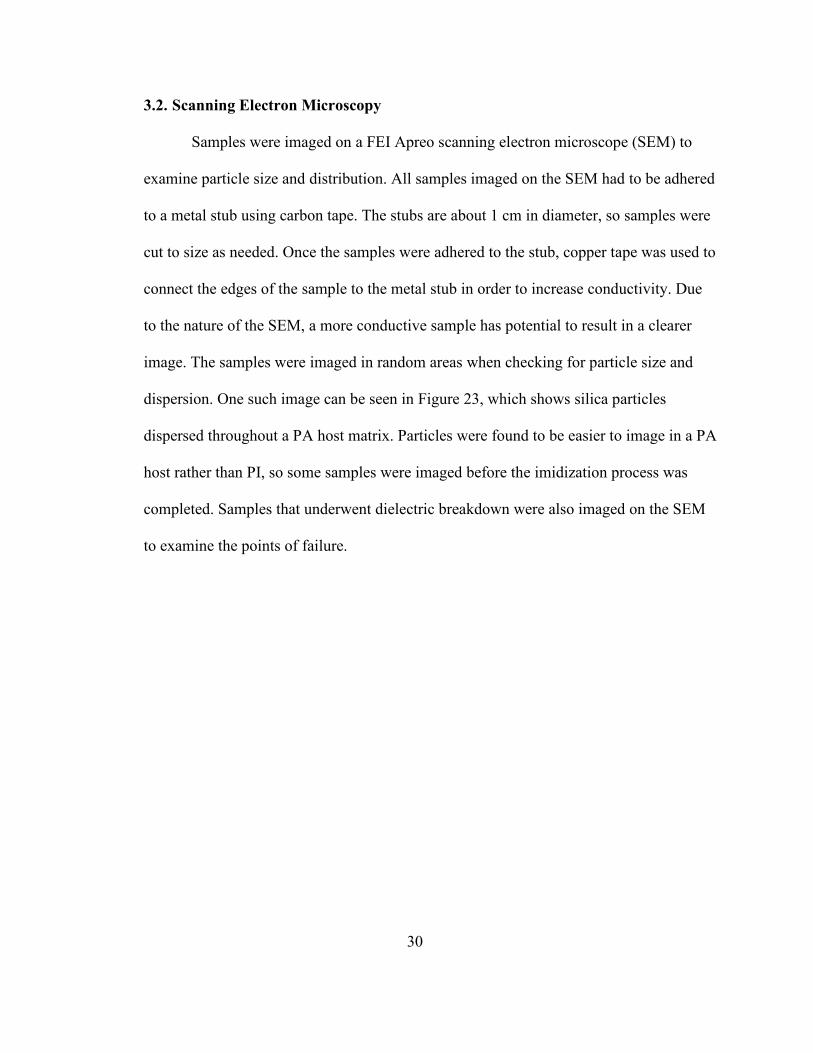
Samples were imaged on a FEI Apreo scanning electron microscope (SEM) to
examine particle size and distribution. All samples imaged on the SEM had to be adhered
to a metal stub using carbon tape. The stubs are about 1 cm in diameter, so samples were
cut to size as needed. Once the samples were adhered to the stub, copper tape was used to
connect the edges of the sample to the metal stub in order to increase conductivity. Due
to the nature of the SEM, a more conductive sample has potential to result in a clearer
image. The samples were imaged in random areas when checking for particle size and
dispersion. One such image can be seen in Figure 23, which shows silica particles
dispersed throughout a PA host matrix. Particles were found to be easier to image in a PA
host rather than PI, so some samples were imaged before the imidization process was
completed. Samples that underwent dielectric breakdown were also imaged on the SEM
to examine the points of failure.
31
Figure 23. SEM image of the surface of a PA/SiO2 composite sample. Silica particles can be seen as dark grey circular masses, with the PA host represented by the lighter grey area.
3.2.1 Energy-Dispersive x-ray spectroscopy. Particles were found difficult to
image given the insulating nature of the PI host matrix. In an effort to combat this,
energy-dispersive x-ray spectroscopy (EDS) was used in tandem with the SEM. The EDS
system provided a means of examining the particles embedded deeper in the host matrix
than the SEM alone, which showed mostly surface-level particles. The EDS system was
capable of isolating singular elements in a material within the imaged area. In the case of
the PI/SiO2 composites, silicon could be selected as the material to be examined, as it was
present in silica but not in PI.
32
Chapter 4
Characterization Results
4.1. Dielectric Strength
Samples with silica concentrations ranging from 0-6%, along with the control
material Kapton, were tested for dielectric strength at 300 K and 92 K. A graph depicting
these results can be seen in Figure 24. The dielectric strength of samples tested at room
temperature can be seen in the striped red bars. Pure PI and 1% PI/SiO2 samples exhibit a
strength of about 275 kV/mm and 250 kV/mm, respectively. Samples with a 2-6% filler
experienced a drop in dielectric strength, averaging around 150 kV/mm at room
temperature. This trend has been seen in previous works and is expected, as there seems
to be an upper limit to the nanofiller concentration [29]. Above this limit, the effect that
silica has on dielectric strength becomes more apparent [56]. Samples of higher
concentrations were initially explored, but were found to contain a non-uniform
dispersion of silica particles. These large pockets of agglomerated particles resulted in
dielectric strengths that varied greatly across a single sample, as well as on a per-sample
basis.
33
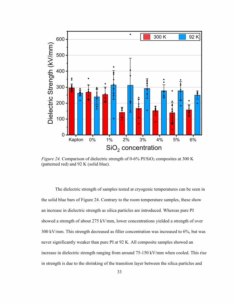
Figure 24. Comparison of dielectric strength of 0-6% PI/SiO2 composites at 300 K (patterned red) and 92 K (solid blue).
The dielectric strength of samples tested at cryogenic temperatures can be seen in
the solid blue bars of Figure 24. Contrary to the room temperature samples, these show
an increase in dielectric strength as silica particles are introduced. Whereas pure PI
showed a strength of about 275 kV/mm, lower concentrations yielded a strength of over
300 kV/mm. This strength decreased as filler concentration was increased to 6%, but was
never significantly weaker than pure PI at 92 K. All composite samples showed an
increase in dielectric strength ranging from around 75-150 kV/mm when cooled. This rise
in strength is due to the shrinking of the transition layer between the silica particles and
0
100
200
300
400
500
600
1%Kapton
SiO2 concentration4% 5% 6%2%0% 3%
Die
lect
ric S
treng
th (k
V/m
m)
300 K 92 K
34
host matrix, owing to the difference in their thermal contraction rates. The change in
temperature results in the PI matrix shrinking at a much faster rate than the SiO2 particles,
causing the host matrix to increase in density and tighten the transition layers around each
nanoparticle. This increase in density limits the electron paths when the sample is under
strong electrical stress. This in turn results in the increase of the voltage required to
achieve breakdown [57].
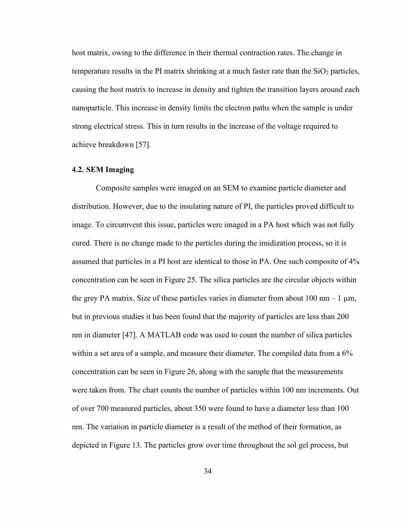
4.2. SEM Imaging
Composite samples were imaged on an SEM to examine particle diameter and
distribution. However, due to the insulating nature of PI, the particles proved difficult to
image. To circumvent this issue, particles were imaged in a PA host which was not fully
cured. There is no change made to the particles during the imidization process, so it is
assumed that particles in a PI host are identical to those in PA. One such composite of 4%
concentration can be seen in Figure 25. The silica particles are the circular objects within
the grey PA matrix. Size of these particles varies in diameter from about 100 nm – 1 µm,
but in previous studies it has been found that the majority of particles are less than 200
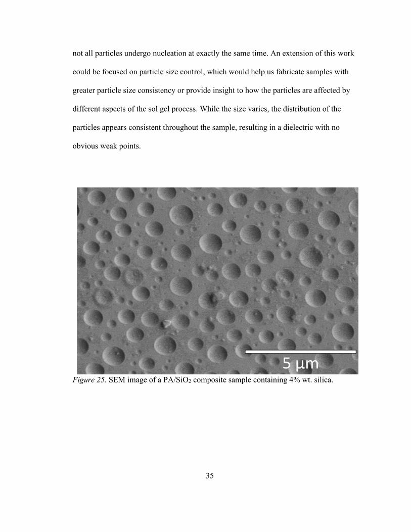
nm in diameter [47]. A MATLAB code was used to count the number of silica particles
within a set area of a sample, and measure their diameter. The compiled data from a 6%
concentration can be seen in Figure 26, along with the sample that the measurements
were taken from. The chart counts the number of particles within 100 nm increments. Out
of over 700 measured particles, about 350 were found to have a diameter less than 100
nm. The variation in particle diameter is a result of the method of their formation, as
depicted in Figure 13. The particles grow over time throughout the sol gel process, but
35
not all particles undergo nucleation at exactly the same time. An extension of this work
could be focused on particle size control, which would help us fabricate samples with
greater particle size consistency or provide insight to how the particles are affected by
different aspects of the sol gel process. While the size varies, the distribution of the
particles appears consistent throughout the sample, resulting in a dielectric with no
obvious weak points.
Figure 25. SEM image of a PA/SiO2 composite sample containing 4% wt. silica.
36
Figure 26. Number of particles within set diameter ranges. Data gathered from an SEM image of a 6% silica sample.
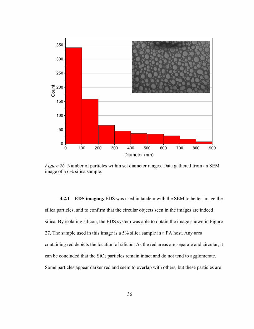
4.2.1 EDS imaging. EDS was used in tandem with the SEM to better image the
silica particles, and to confirm that the circular objects seen in the images are indeed
silica. By isolating silicon, the EDS system was able to obtain the image shown in Figure
27. The sample used in this image is a 5% silica sample in a PA host. Any area
containing red depicts the location of silicon. As the red areas are separate and circular, it
can be concluded that the SiO2 particles remain intact and do not tend to agglomerate.
Some particles appear darker red and seem to overlap with others, but these particles are
0 100 200 300 400 500 600 700 800 9000
50
100
150
200
250
300
350
Cou
nt
Diameter (nm)
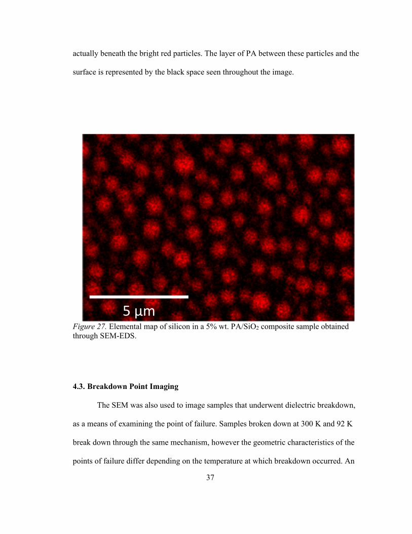
37
actually beneath the bright red particles. The layer of PA between these particles and the
surface is represented by the black space seen throughout the image.
Figure 27. Elemental map of silicon in a 5% wt. PA/SiO2 composite sample obtained through SEM-EDS.
4.3. Breakdown Point Imaging
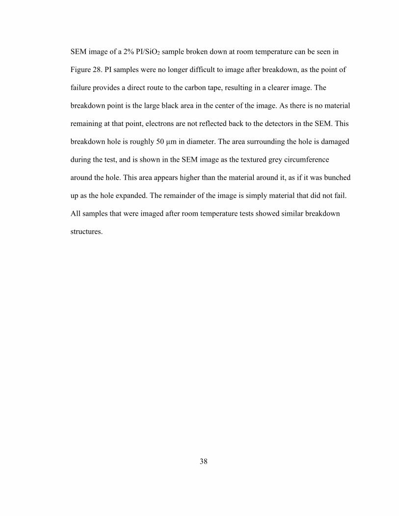
The SEM was also used to image samples that underwent dielectric breakdown,
as a means of examining the point of failure. Samples broken down at 300 K and 92 K
break down through the same mechanism, however the geometric characteristics of the
points of failure differ depending on the temperature at which breakdown occurred. An
5 µm
38
SEM image of a 2% PI/SiO2 sample broken down at room temperature can be seen in
Figure 28. PI samples were no longer difficult to image after breakdown, as the point of
failure provides a direct route to the carbon tape, resulting in a clearer image. The
breakdown point is the large black area in the center of the image. As there is no material
remaining at that point, electrons are not reflected back to the detectors in the SEM. This
breakdown hole is roughly 50 µm in diameter. The area surrounding the hole is damaged
during the test, and is shown in the SEM image as the textured grey circumference
around the hole. This area appears higher than the material around it, as if it was bunched
up as the hole expanded. The remainder of the image is simply material that did not fail.
All samples that were imaged after room temperature tests showed similar breakdown
structures.
39
Figure 28. SEM image of a breakdown point within a 2% PI/SiO2 composite sample broken down at 300 K.
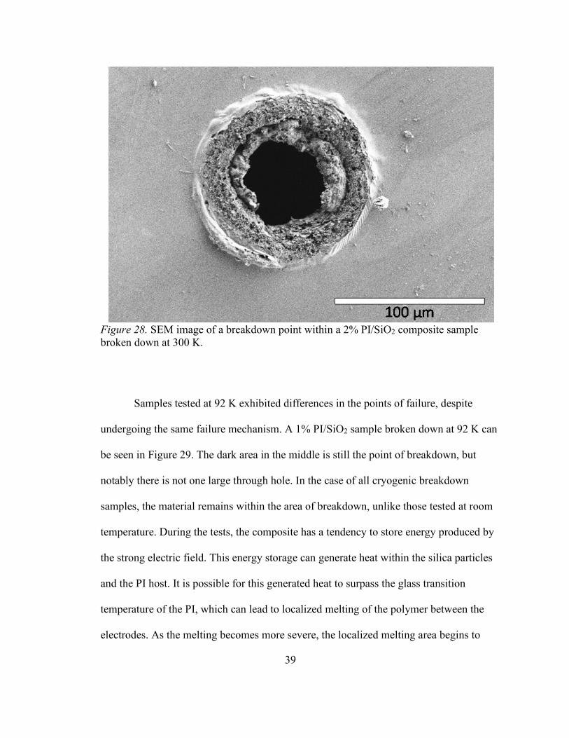
Samples tested at 92 K exhibited differences in the points of failure, despite
undergoing the same failure mechanism. A 1% PI/SiO2 sample broken down at 92 K can
be seen in Figure 29. The dark area in the middle is still the point of breakdown, but
notably there is not one large through hole. In the case of all cryogenic breakdown
samples, the material remains within the area of breakdown, unlike those tested at room
temperature. During the tests, the composite has a tendency to store energy produced by
the strong electric field. This energy storage can generate heat within the silica particles
and the PI host. It is possible for this generated heat to surpass the glass transition
temperature of the PI, which can lead to localized melting of the polymer between the
electrodes. As the melting becomes more severe, the localized melting area begins to
40
grow, forming a large amorphous area [58]. It is this large amorphous area that causes the
through holes seen in samples tested at 300 K.
Figure 29. SEM image of a point of breakdown within a 1% PI/SiO2 composite sample, tested at 92 K.
The localized heating resulting from the strong electric field is present in samples
tested cryogenically, but the cold environment inhibits the polymer’s tendency to exceed
the glass transition temperature. Therefore, in a cryogenic environment, PI can break
down while remaining solid [59]. The lower starting temperature of the PI results in a
higher energy and heat requirement to reach the glass transition temperature, a
requirement which the hipot cannot meet. Additionally, the cryogenic environment
41
allows for the heat generated within the sample to dissipate rapidly. As a result of these
factors, samples broken down at cryogenic temperatures exhibit different breakdown
geometries, specifically the lack of a through hole at the point of failure.
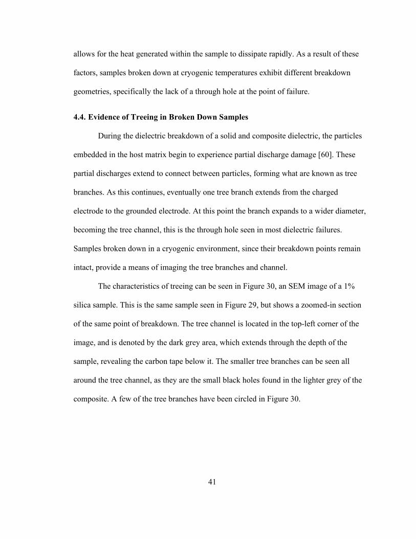
4.4. Evidence of Treeing in Broken Down Samples
During the dielectric breakdown of a solid and composite dielectric, the particles
embedded in the host matrix begin to experience partial discharge damage [60]. These
partial discharges extend to connect between particles, forming what are known as tree
branches. As this continues, eventually one tree branch extends from the charged
electrode to the grounded electrode. At this point the branch expands to a wider diameter,
becoming the tree channel, this is the through hole seen in most dielectric failures.
Samples broken down in a cryogenic environment, since their breakdown points remain
intact, provide a means of imaging the tree branches and channel.
The characteristics of treeing can be seen in Figure 30, an SEM image of a 1%
silica sample. This is the same sample seen in Figure 29, but shows a zoomed-in section
of the same point of breakdown. The tree channel is located in the top-left corner of the
image, and is denoted by the dark grey area, which extends through the depth of the
sample, revealing the carbon tape below it. The smaller tree branches can be seen all
around the tree channel, as they are the small black holes found in the lighter grey of the
composite. A few of the tree branches have been circled in Figure 30.
42
Figure 30. Close inspection of the material damaged in a cryogenic dielectric test, using a zoomed-in view of the 1% PI/SiO2 sample in Figure 29.
43
Chapter 5
Cryogenic Testing Chamber
5.1. Design Considerations
The helium chamber’s primary goal is to cool samples and equipment to 40 K, so
that testing can be carried out in a cryogenic environment. The first factor to be
considered for any design is safety. In the case of a helium-cooled cryogenic chamber,
safety can be broken up into four categories: pressure build-up, gas leaks, electrical
discharge, and temperature exposure. Pressure build-up can occur when a gas is being fed
into a chamber, but fails to exit into the larger system. According to ASME standards, the
maximum stress that is exerted during a pressure vessel’s operation should not exceed 2/3
of the yield strength of the material [61, 62]. Gas leaks most often occur at a joint where
two materials meet, usually either with a weld or a flange. There are tools used to detect
trace amounts of gas, such as a helium sniffer. If the chamber is filled with helium, the
helium sniffer can be used around the outside of the chamber to detect any leaks in the
system. Electrical discharge is largely accounted for in the dielectric testing rig, but in the
case of its failure, the entire chamber can be grounded. This can be as simple as
connecting a wire to the chamber which plugs into the ground prong of an electric socket.
Finally, to satisfy any concerns regarding temperature exposure, the chamber containing
the cryogenic environment will be encased in a vacuum jacket and have limited
penetrations leading to the outside environment. These efforts will work to minimize the
amount of convective and conductive heat transfer. Further, any persons near the
chamber will wear cryogenic gloves and exercise caution during operation.
44
The helium cooling and circulation systems were provided for this research by the
Applied Superconductivity Team at the NSWCPD. Only the chamber in which the
dielectric and CTE testing remains, as can be seen in Figure 31. The Turbo Lab tabletop
vacuum pump was purchased from Leybold GmbH, and the helium canister was
purchased from Airgas. The cryocooler provided has input and output cryogenic transfer
hoses, which end in male bayonet fittings. Therefore, in order to work with the provided
system, the test chamber must have input and output female bayonet fittings. These
fittings are the only restrictions that the existing system placed on the test chamber. The
fan, which is located on the cryocooler, is capable of spinning at a rate of 300 Hz.
However, many factors of the cryocooler are unknown, so the mass flow rate of the
system is uncertain.
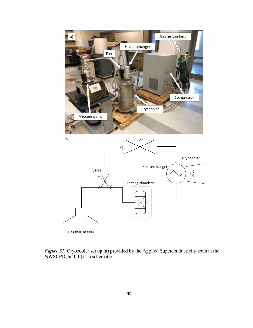
45
Figure 31. Cryocooler set up (a) provided by the Applied Superconductivity team at the NWSCPD, and (b) as a schematic.
Gas helium tank
Compressor
Cryocooler
Vacuum pump
Fan
Heat exchanger
a)
Gas helium tank
b)
Valve
Fan
Heat exchanger
Cryocooler
Testing chamber
46
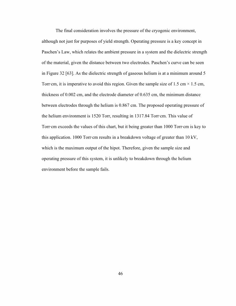
The final consideration involves the pressure of the cryogenic environment,
although not just for purposes of yield strength. Operating pressure is a key concept in
Paschen’s Law, which relates the ambient pressure in a system and the dielectric strength
of the material, given the distance between two electrodes. Paschen’s curve can be seen
in Figure 32 [63]. As the dielectric strength of gaseous helium is at a minimum around 5
Torr‧cm, it is imperative to avoid this region. Given the sample size of 1.5 cm × 1.5 cm,
thickness of 0.002 cm, and the electrode diameter of 0.635 cm, the minimum distance
between electrodes through the helium is 0.867 cm. The proposed operating pressure of
the helium environment is 1520 Torr, resulting in 1317.84 Torr‧cm. This value of
Torr‧cm exceeds the values of this chart, but it being greater than 1000 Torr‧cm is key to
this application. 1000 Torr‧cm results in a breakdown voltage of greater than 10 kV,
which is the maximum output of the hipot. Therefore, given the sample size and
operating pressure of this system, it is unlikely to breakdown through the helium
environment before the sample fails.
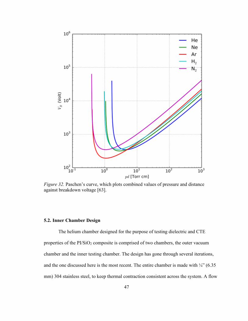
47
Figure 32. Paschen’s curve, which plots combined values of pressure and distance against breakdown voltage [63].
5.2. Inner Chamber Design
The helium chamber designed for the purpose of testing dielectric and CTE
properties of the PI/SiO2 composite is comprised of two chambers, the outer vacuum
chamber and the inner testing chamber. The design has gone through several iterations,
and the one discussed here is the most recent. The entire chamber is made with ¼” (6.35
mm) 304 stainless steel, to keep thermal contraction consistent across the system. A flow
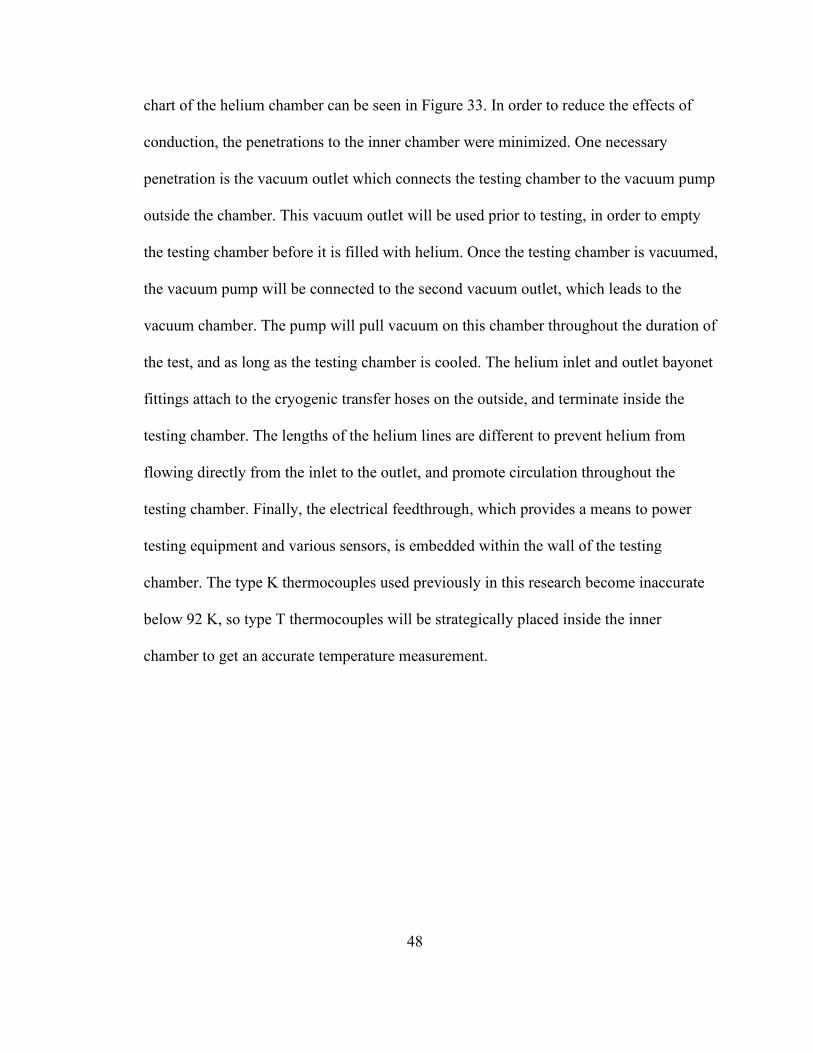
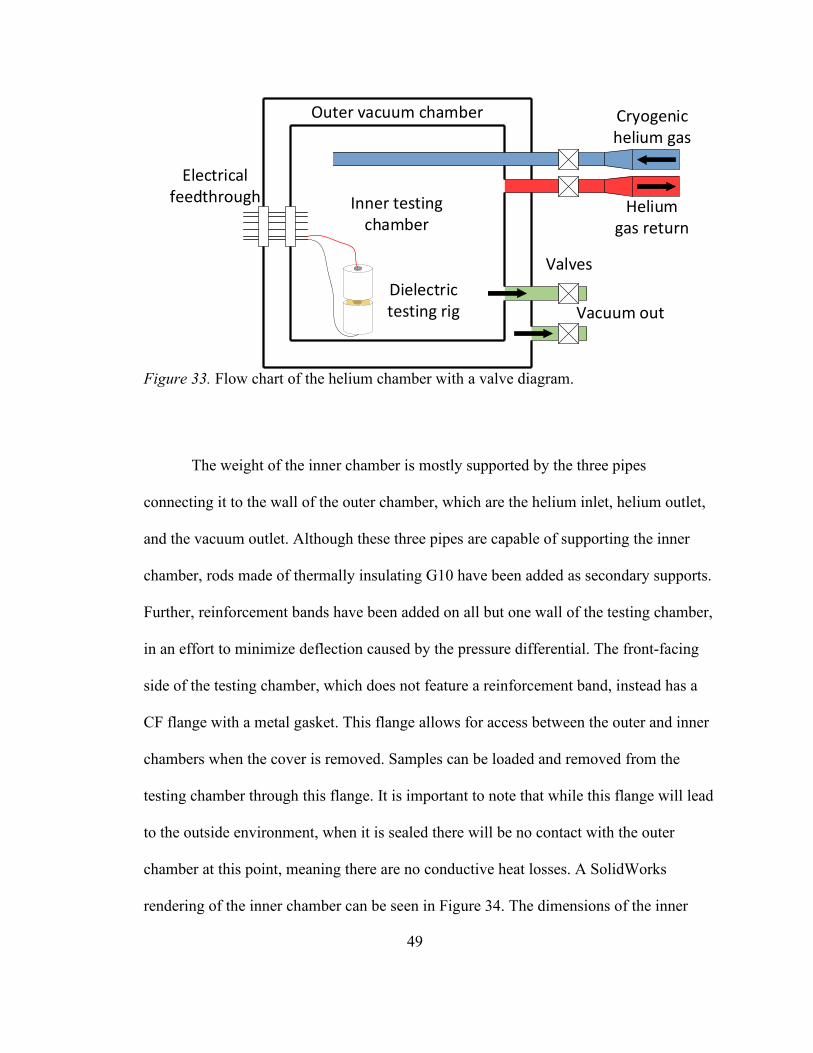
48
chart of the helium chamber can be seen in Figure 33. In order to reduce the effects of
conduction, the penetrations to the inner chamber were minimized. One necessary
penetration is the vacuum outlet which connects the testing chamber to the vacuum pump
outside the chamber. This vacuum outlet will be used prior to testing, in order to empty
the testing chamber before it is filled with helium. Once the testing chamber is vacuumed,
the vacuum pump will be connected to the second vacuum outlet, which leads to the
vacuum chamber. The pump will pull vacuum on this chamber throughout the duration of
the test, and as long as the testing chamber is cooled. The helium inlet and outlet bayonet
fittings attach to the cryogenic transfer hoses on the outside, and terminate inside the
testing chamber. The lengths of the helium lines are different to prevent helium from
flowing directly from the inlet to the outlet, and promote circulation throughout the
testing chamber. Finally, the electrical feedthrough, which provides a means to power
testing equipment and various sensors, is embedded within the wall of the testing
chamber. The type K thermocouples used previously in this research become inaccurate
below 92 K, so type T thermocouples will be strategically placed inside the inner
chamber to get an accurate temperature measurement.
49
Figure 33. Flow chart of the helium chamber with a valve diagram.
The weight of the inner chamber is mostly supported by the three pipes
connecting it to the wall of the outer chamber, which are the helium inlet, helium outlet,
and the vacuum outlet. Although these three pipes are capable of supporting the inner
chamber, rods made of thermally insulating G10 have been added as secondary supports.
Further, reinforcement bands have been added on all but one wall of the testing chamber,
in an effort to minimize deflection caused by the pressure differential. The front-facing
side of the testing chamber, which does not feature a reinforcement band, instead has a
CF flange with a metal gasket. This flange allows for access between the outer and inner
chambers when the cover is removed. Samples can be loaded and removed from the
testing chamber through this flange. It is important to note that while this flange will lead
to the outside environment, when it is sealed there will be no contact with the outer
chamber at this point, meaning there are no conductive heat losses. A SolidWorks
rendering of the inner chamber can be seen in Figure 34. The dimensions of the inner
Inner testing chamber
Outer vacuum chamber
Electrical feedthrough
Vacuum out
Cryogenic helium gas
Helium gas return
ValvesDielectric testing rig
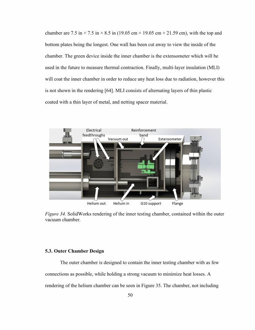
50
chamber are 7.5 in × 7.5 in × 8.5 in (19.05 cm × 19.05 cm × 21.59 cm), with the top and
bottom plates being the longest. One wall has been cut away to view the inside of the
chamber. The green device inside the inner chamber is the extensometer which will be
used in the future to measure thermal contraction. Finally, multi-layer insulation (MLI)
will coat the inner chamber in order to reduce any heat loss due to radiation, however this
is not shown in the rendering [64]. MLI consists of alternating layers of thin plastic
coated with a thin layer of metal, and netting spacer material.
Figure 34. SolidWorks rendering of the inner testing chamber, contained within the outer vacuum chamber.
5.3. Outer Chamber Design
The outer chamber is designed to contain the inner testing chamber with as few
connections as possible, while holding a strong vacuum to minimize heat losses. A
rendering of the helium chamber can be seen in Figure 35. The chamber, not including
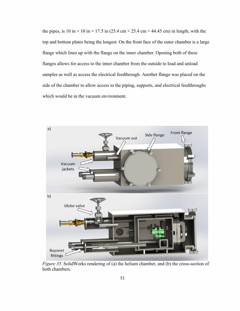
51
the pipes, is 10 in × 10 in × 17.5 in (25.4 cm × 25.4 cm × 44.45 cm) in length, with the
top and bottom plates being the longest. On the front face of the outer chamber is a large
flange which lines up with the flange on the inner chamber. Opening both of these
flanges allows for access to the inner chamber from the outside to load and unload
samples as well as access the electrical feedthrough. Another flange was placed on the
side of the chamber to allow access to the piping, supports, and electrical feedthroughs
which would be in the vacuum environment.
Figure 35. SolidWorks rendering of (a) the helium chamber, and (b) the cross-section of both chambers.
52
There are four pipes connecting to the rear of the outer chamber, which are two
bayonet fittings contained in vacuum jackets, a KF fitting which attaches to the vacuum
pump, and a cryogenic globe valve in a vacuum jacket. The globe valve will be used to
control the flow when the inner chamber is being vacuumed, prior to tests. All vacuum
jackets are connected to the vacuum contained in the outer chamber, meaning that they
will be under an actively pulled vacuum for the duration of all tests. The pipes used for
transfer of gaseous helium and connecting vacuum lines are all Schedule 40 stainless
steel, with a ½” (12.7 mm) diameter.
5.4. Chamber Simulations
There are two main concerns regarding failure in the helium chamber, the
operating pressure in the testing chamber, and the deflection of the pipes supporting the
testing chamber. In order to address these concerns, simulations were run on SolidWorks
to determine the amount of deflection and stress created by each of these factors. A
simulation of the effects of operating pressure on the inner chamber walls can be seen in
Figure 36. Given an operating pressure of 1520 Torr, and the dimensions of the 21.59 cm
× 19.05 cm × 0.635 cm plates, the maximum deflection and stress can be modeled on a
color scale. The maximum deflection was found to be 0.086 mm, while the maximum
stress was 46.68 MPa. Assuming the yield strength of the stainless steel plates is 206.84
MPa, the resulting factor of safety is 4.43 [65]. Simulations were verified by a calculation
program through MITCalc, which calculated a maximum deflection of 0.085 mm, and a
maximum stress of 65.33 MPa [66]. These simulations were run prior to the addition of
the reinforcement bands, which should reduce the deflection of the plates.
53
Figure 36. SolidWorks simulation of the effects of 1520 Torr operating pressure on the (a) deflection of the inner chamber, and (b) stress of the inner chamber.
The deflection of the pipes that support the weight of the inner chamber was also
simulated to determine the maximum deflection and stress. Although the G10 supports
will minimize the chamber’s downward deflection, this simulation was run assuming
those supports failed. Further, this simulation is of a single pipe, where in reality there
will be three pipes taking the weight of the inner chamber. The results of this simulation
can be seen in Figure 37. The Schedule 40 pipes have a ½” (12.7 mm) diameter, and the
force of the inner chamber due to gravity was calculated to be 154.45 N. The simulated
maximum deflection is 0.00891 mm, while the maximum stress is 83.47 MPa. Given a
yield strength of 200.33 MPa, the resulting factor of safety is 2.4. Simulation results were
verified via Roark’s equation of stress for a beam which is fixed on one end and has a
load at the other. Through this method, maximum deflection was found to be 0.00768
mm [67].
a) b)
54
Figure 37. SolidWorks simulation of the effects of 154.45 N weight on (a) the deflection of a single pipe, and (b) the stress of a single pipe.
The design described herein is the latest of several iterations, and is the final as
the manufacturing phase begins. However, it is expected that the design may undergo
minor changes as it is manufactured if issues become apparent. As the chamber is to be
built in-house, many pieces will be cut from larger bulk material. Many features are
welded together, such as the chamber walls and vacuum jackets. Upon its completion, the
project can move into the next and final phase: material testing in a helium-cooled
cryogenic environment.
55
Chapter 6
Conclusions and Future Works
6.1. Summary
In this thesis, a potential dielectric for use on helium-cooled high-temperature
superconducting cables is explored. Silicon dioxide is used as a nanoparticle filler inside
of a polyimide host matrix. Given the right concentration of SiO2, the composite will
potentially have sufficient dielectric strength while matching the thermal contraction rate
of the HTS cable. Composites were generated through both an ex situ and an in situ
process, until in situ samples were found to have better dispersion and less particle
agglomeration. The composites are prepared in the form of thin films, averaging 20 µm
in thickness, for the characterization of their properties.
Composite samples were tested and examined through two main methods:
dielectric breakdown testing and scanning electron microscopy. Dielectric breakdown
tests occurred at both 300 K and 92 K. Tests performed at 92 K took place within a dewar
containing liquid nitrogen, but the samples were not submerged in the LN2. The samples
showed a clear increase in dielectric strength when tested at cryogenic temperatures,
which is attributed to the contraction of the polymer resulting in an increased density.
Samples tested at room temperature averaged a dielectric strength of 175 kV/mm, while
samples broken down in a cryogenic environment had an average dielectric strength of
275 kV/mm. Images taken on the SEM revealed uniform dispersion of the particles, as
well as the particle size distribution. The majority of the nanoparticles were found to be
less than 200 nm in diameter. Further, samples broken down at 92 K showed evidence of
56
treeing, a breakdown mechanism which involves the partial breakdown of a sample
before failure occurs.
A helium-cooled cryogenic chamber was designed to house the testing equipment
for dielectric breakdown and thermal contraction testing of the composites. This chamber
should achieve temperatures lower than that of liquid nitrogen, and allow for tests similar
to the composite’s environment on the HTS cables. The helium chamber consists of the
inner chamber, which is filled with helium and contained within the second chamber, the
vacuum chamber. The vacuum surrounding the inner chamber will mitigate any
convectional heat loss, while limited connections work to reduce heat loss caused by
conduction. Finally, multi-layer insulation will be used to reduce any heat loss due to
radiation. This design is the latest of many iterations, and it will continue to be improved
as the fabrication process begins.
The research performed herein provides insight to the fields of research involving
nanocomposites, dielectric breakdown, and HTS cables aboard Navy ships. Throughout
this research, works have been published describing the in situ fabrication process,
providing a detailed set of instructions for the generation of PI/SiO2 composites. Further,
the behavior of the composites has also been discussed in these published works,
specifically the performance in a cryogenic environment [68]. A dielectric strength
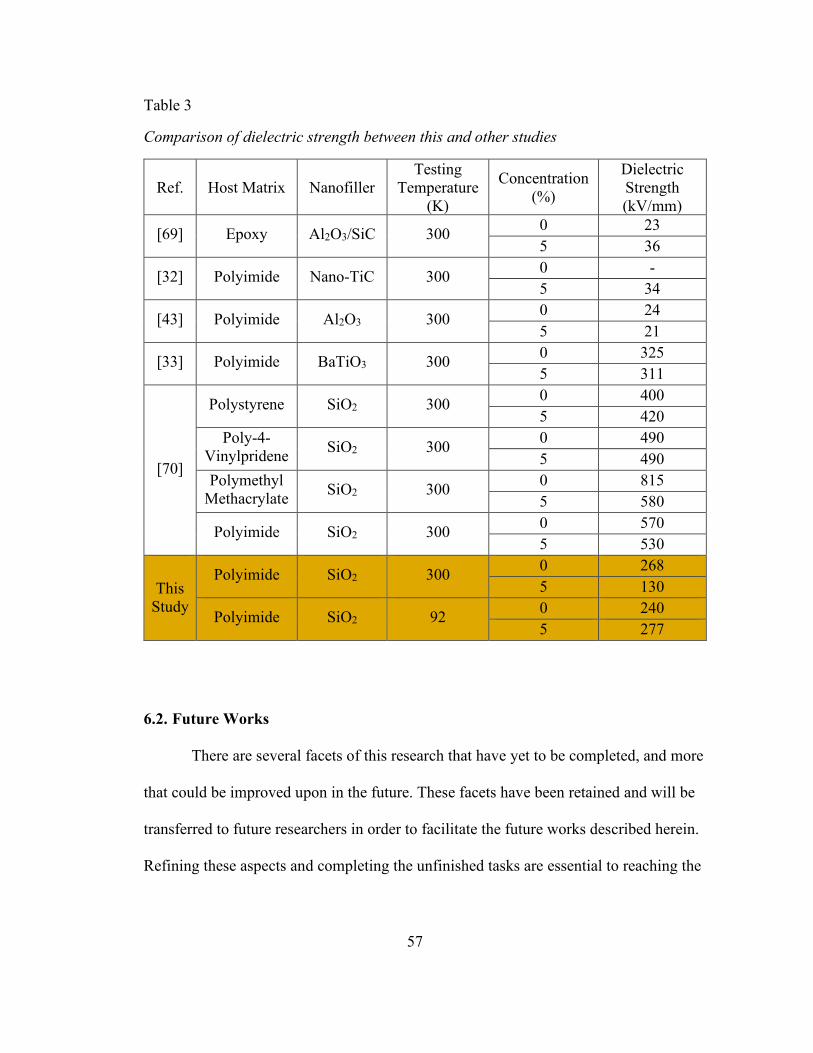
comparison table can be seen in Table 3. The evidence of electrical treeing shown in
Chapter 4 is fairly unique, as published works on this subject are limited. Finally, the
work reported here has advanced Naval research involving HTS cables in a gaseous
helium-cooled cryogenic environment. While not resolved, this issue is now better
understood, and a solution seems more possible than ever before.
57
Table 3
Comparison of dielectric strength between this and other studies
Ref.
Host Matrix
Nanofiller
Testing Temperature
(K)
Concentration (%)
Dielectric Strength (kV/mm)
[69]
Epoxy
Al2O3/SiC
300 0 23 5 36
[32]
Polyimide
Nano-TiC
300 0 - 5 34
[43]
Polyimide
Al2O3
300 0 24 5 21
[33]
Polyimide
BaTiO3
300 0 325 5 311
[70]
Polystyrene
SiO2
300 0 400 5 420
Poly-4-Vinylpridene
SiO2
300 0 490 5 490
Polymethyl Methacrylate
SiO2
300 0 815 5 580
Polyimide
SiO2
300 0 570 5 530
This Study
Polyimide
SiO2
300 0 268 5 130
Polyimide
SiO2
92 0 240 5 277
6.2. Future Works
There are several facets of this research that have yet to be completed, and more
that could be improved upon in the future. These facets have been retained and will be
transferred to future researchers in order to facilitate the future works described herein.
Refining these aspects and completing the unfinished tasks are essential to reaching the
58
end goal of this research, to coat an HTS cable with a PI/SiO2 composite for use in a
helium-cooled cryogenic environment.
1) Polyimide was chosen due to its strong dielectric strength and ease of use in a
laboratory setting. However, the high imidization temperature of PI is not safe
for HTS cable production. Given more time, another polymer should be
explored as the host matrix. A comparative study could be conducted to
determine if a different host polymer is more suitable for this application.
2) There are many factors to the in situ fabrication process. In the future, these
factors can be adjusted in a parametric study in an effort to create more
consistent silica particles. Greater consistency of particle diameter could
potentially affect the properties of the composite material, as the particles
above 100 nm in diameter may not have the same properties as those that are
true nanoscale particles with diameter < 100 nm. Some factors that could be
altered include but are not limited to: the time spent mixing the precursors
separately, the time spent mixing the sol gel within PAA, and the ambient
temperature during the mixing process.
3) All composite samples that underwent dielectric breakdown did so in a timely
manner, relative to their fabrication. Ideally, a shelf life study could be
conducted, in which samples created in one batch would be tested over time.
A study such as this could determine if the properties of the composite change
over time when not in use. The results found in this study would reveal
whether or not the composite would need to be replaced on HTS cables, and
how often.

59
4) Electron microscopy can be used to further examine the points of dielectric
breakdown in the samples. Specifically, the particles contained within the area
damaged by breakdown should be examined for any changes, such as
sintering. Imaging the changes that these particles may undergo could lead to
a greater understanding of the breakdown process and its lasting effects on a
material.
5) The design of the helium chamber has been completed, and the next step in its
completion is the manufacturing phase. During this phase, it is expected that
minor issues will arise. For this reason, the manufacturing phase must be
flexible, as improvements will need to be made to account for these flaws.
Any improvement made to the chamber makes reaching the goal of 40 K more
feasible.
6) The successful manufacture of the testing chamber will allow for testing of the
effects of thermal cycling on the composite. Following a number of cooling
cycles, the composite’s dielectric strength and thermal contraction rate could
be tested to determine if thermal cycling has an effect on these properties. The
number of cooling cycles that take place prior to testing could be varied to
produce more thorough results.
7) The composites are currently made in the form of thin films, which will need
to change in order to be applied as the final product. One of the next major
phases of this research is to develop a method to coat and cure the composite
on a wire. Polymer extrusion is a common method used in the industry to coat
wires, which involves pulling the wire through a vat filled with the polymer
60
which is used to coat the wire. Once coated, the wire moves through an oven
to heat and cure the polymer in place. This method would be scalable, so that
it could first be tested in a laboratory setting, then used on the full scale HTS
cables, which may be as long as 100 feet.
8) Successfully coating a wire opens up two new testing methods. First, a coated
wire could be placed in the chamber to be cooled and heated back to room
temperature. Doing so would allow for the inspection of any failures in the
composite caused by thermal cycling. Further, dielectric testing can be
conducted on a coated wire. Testing could be performed using the point-plane
method, in which a pointed electrode is pressed to the surface of the polymer
on a wire, and the wire is grounded. A decrease in dielectric strength is
expected when coating a wire in a dielectric, but the exact amount of the
decrease is a key factor which should be determined. Achieving this, along
with the other future works, moves this research closer to completion, and
increases feasibility of implementation on HTS cables aboard Navy ships.
61
References
[1] SuperPower Inc. "HTS TRANSMISSION CABLE." http://www.superpower-inc.com/.
[2] R. Cava et al., "Superconductivity in the quaternary intermetallic compounds LnNi2B2C," Nature, vol. 367, pp. 252-253, 01/20 1994.
[3] Robert A. Hawsey and Satoshi Morozumi, "The Energy and Environmental Benefits of Superconducting Power Products," Mitigation and Adaptation Strategies for Global Change, vol. 10, no. 2, pp. 279-306, 2005/04/01 2005.
[4] J. P. Stovall et al., "Installation and operation of the Southwire 30-meter high-temperature superconducting power cable," IEEE Transactions on Applied Superconductivity, vol. 11, no. 1, pp. 2467-2472, 2001.
[5] D. Lindsay, M. Roden, Dag Willen, Albert Keri, and B. Mehraban, "Operating experience of 13.2 kV superconducting cable system at AEP bixby station," vol. CIGRÉ, pp. B1-107, 08/20 2008.
[6] Office of Naval Research, "Office of Naval Research Demonstrates Revolutionary New Counter-Mine Technology for Ships," ed, 2009.
[7] R. A. Marshall, "The distributed energy store railgun, its efficiency, and its energy store implications," IEEE Transactions on Magnetics, vol. 33, no. 1, pp. 582-588, 1997.
[8] Ronggang Cao and Guangwei Zhang, "Analysis of current characteristics of the electromagnetic rail gun based on HHT," IEEJ Transactions on Electrical and Electronic Engineering, vol. 13, no. 2, pp. 339-340, 2018.
[9] John J. Holmes, Reduction of a ship's magnetic field signatures (Synthesis lectures on computational electromagnetics, #23). San Rafael, Calif. (1537 Fourth Street, San Rafael, CA 94901 USA): Morgan & Claypool Publishers, 2008.
[10] Thomas H. Fikse Brian K. Fitzpatrick, William A. Lynch, "High temperature superconducting degaussing system," United States Patent Appl. 11/788,331, 2008.
62
[11] F. Le Dorze, J. P. Bongiraud, J. L. Coulomb, P. Labie, and X. Brunotte, "Modeling of degaussing coils effects in ships by the method of reduced scalar potential jump," IEEE Transactions on Magnetics, vol. 34, no. 5, pp. 2477-2480, 1998.
[12] J. T. Kephart, B. K. Fitzpatrick, P. Ferrara, M. Pyryt, J. Pienkos, and E. M. Golda, "High Temperature Superconducting Degaussing From Feasibility Study to Fleet Adoption," IEEE Transactions on Applied Superconductivity, vol. 21, no. 3, pp. 2229-2232, 2011.
[13] National Musem of the Royal New Zealand Navy. "Degaussing Ships." http://navymuseum.co.nz/.
[14] B. K. Fitzpatrick, J. T. Kephartl, and E. M. Golda, "Characterization of Gaseous Helium Flow Cryogen in a Flexible Cryostat for Naval Applications of High Temperature Superconductors," IEEE Transactions on Applied Superconductivity, vol. 17, no. 2, pp. 1752-1755, 2007.
[15] (2007). A National Effort to Introduce New Technology into the Power Delivery Infrastructure.
[16] H. Yumura et al., "Phase II of the Albany HTS Cable Project," IEEE Transactions on Applied Superconductivity, vol. 19, no. 3, pp. 1698-1701, 2009.
[17] H. Yumura et al., "In-grid demonstration of long-length "3-in-0ne" HTS cable (Albany Project)," SEI Technical Review, pp. 69-79, 04/01 2009.
[18] M. Santosh, "The Promising Role of Superconductivity in Cable Power Applications," Journal of Electrical Engineering, vol. 6, pp. 295-298, 2018.
[19] C. Gu, Y. Zhang, F. Li, and W. Yuan, "Economic analysis of interconnecting distribution substations via superconducting cables," in 2012 IEEE Power and Energy Society General Meeting, 22-26 July 2012 2012, pp. 1-5.
[20] W. Yuan, S. Venuturumilli, Z. Zhang, Y. Mavrocostanti, and M. Zhang, "Economic Feasibility Study of Using High-Temperature Superconducting Cables in U.K.'s Electrical Distribution Networks," IEEE Transactions on Applied Superconductivity, vol. 28, no. 4, pp. 1-5, 2018.
63
[21] M. Kosaki, "Research and development of electrical insulation of superconducting cables by extruded polymers," IEEE Electrical Insulation Magazine, vol. 12, no. 5, pp. 17-24, 1996.
[22] M. Kosaki, M. Nagao, Y. Mizuno, N. Shimizu, and K. Horii, "Development of extruded polymer insulated superconducting cable," Cryogenics, vol. 32, no. 10, pp. 885-894, 1992/01/01/ 1992.
[23] J. F. Heacock and C. E. Berr, "Polyimides—new high temperature polymers: H-film, a polypyromellitimide film," Polymer Engineering & Science, vol. 5, no. 2, pp. 105-110, 1965.
[24] Jack Ekin and George Zimmerman, "Experimental Techniques for Low-Temperature Measurements: Cryostat Design, Material Properties, and Superconductor Critical-Current Testing," Physics Today - PHYS TODAY, vol. 60, 05/01 2007.
[25] Uday Burman and Praveen Kumar, "Chapter 5 - Plant Response to Engineered Nanoparticles," in Nanomaterials in Plants, Algae, and Microorganisms, D. K. Tripathi, P. Ahmad, S. Sharma, D. K. Chauhan, and N. K. Dubey Eds.: Academic Press, 2018, pp. 103-118.
[26] Anna C. Balazs, Todd Emrick, and Thomas P. Russell, "Nanoparticle Polymer Composites: Where Two Small Worlds Meet," Science, vol. 314, no. 5802, pp. 1107-1110, 2006.
[27] Masakatsu Kochi, Rikio Yokota, Taka Yuki Iizuka, and Itaru Mita, "Improving tensile mechanical properties of aromatic polyimides by thermal imidization after cold drawing of poly (amic acids)," Journal of Polymer Science Part B: Polymer Physics, vol. 28, no. 13, pp. 2463-2472, 1990.
[28] Sigma-Aldrich. Poly(pyromellitic dianhydride-co-4,4'-oxydianiline), amic acid solution [Online] Available: https://www.sigmaaldrich.com/united-states.html
[29] X. Cui et al., "Mechanical and dielectric properties of polyimide/silica nanocomposite films," Plastics, Rubber & Composites, Article vol. 44, no. 10, pp. 435-439, 2015.
64
[30] Young-Jae Kim, Jong-Heon Kim, Shin-Woo Ha, Dongil Kwon, and Jin-Kyu Lee, "Polyimide nanocomposites with functionalized SiO2 nanoparticles: enhanced processability, thermal and mechanical properties," RSC Advances, 10.1039/C4RA04952G vol. 4, no. 82, pp. 43371-43377, 2014.
[31] Der-Jang Liaw, Kung-Li Wang, Ying-Chi Huang, Kueir-Rarn Lee, Juin-Yih Lai, and Chang-Sik Ha, "Advanced polyimide materials: Syntheses, physical properties and applications," Progress in Polymer Science, vol. 37, no. 7, pp. 907-974, 2012/07/01/ 2012.
[32] Qian-shan Xia, Ling Weng, Li-wen Yan, Li-zhu Liu, Mao-chang Cao, and Jun-wang Liu, "Preparation and dielectric properties of nano-TiC/polyimide composite films as embedded-capacitor application," in Ifost, 28 June-1 July 2013 2013, vol. 1, pp. 230-232.
[33] Shuangshuang Yue, Baoquan Wan, Yunying Liu, and Qiwei Zhang, "Significantly enhanced dielectric constant and energy storage properties in polyimide/reduced BaTiO3 composite films with excellent thermal stability," RSC Advances, 10.1039/C8RA10434D vol. 9, no. 14, pp. 7706-7717, 2019.
[34] Y. Z. Hu, D. J. Diehl, Q. Liu, C. Y. Zhao, and E. A. Irene, "In situ real time measurement of the incubation time for silicon nucleation on silicon dioxide in a rapid thermal process," Applied Physics Letters, vol. 66, no. 6, pp. 700-702, 1995.
[35] K. Achuthan, J. Curry, M. Lacy, D. Campbell, and S. V. Babu, "Investigation of pad deformation and conditioning during the CMP of silicon dioxide films," Journal of Electronic Materials, vol. 25, no. 10, pp. 1628-1632, 1996/10/01 1996.
[36] C. J. Huang, S. Y. Fu, Y. H. Zhang, B. Lauke, L. F. Li, and L. Ye, "Cryogenic properties of SiO2/epoxy nanocomposites," Cryogenics, vol. 45, no. 6, pp. 450-454, 2005/06/01/ 2005.
[37] K. P. Chow and G. A. Millos, "Measurements of modulus of elasticity and thermal contraction of epoxy impregnated niobium-tin and niobium-titanium composites," IEEE Transactions on Applied Superconductivity, vol. 9, no. 2, pp. 213-215, 1999.
[38] Paul R Gray, Paul Hurst, Robert G Meyer, and Stephen Lewis, Analysis and design of analog integrated circuits. Wiley, 2001.
65
[39] Pavel V. Komarov, Yu-Tsung Chiu, Shih-Ming Chen, and Peter Reineker, "Investigation of Thermal Expansion of Polyimide/SiO2 Nanocomposites by Molecular Dynamics Simulations," Macromolecular Theory and Simulations, vol. 19, no. 1, pp. 64-73, 2010.
[40] Chul Han Kim, Sung-Kyu Kim, Lukas Graber, and Sastry V. Pamidi, "Cryogenic Thermal Studies on Terminations for Helium Gas Cooled Superconducting Cables," Physics Procedia, vol. 67, pp. 201-207, 2015/01/01/ 2015.
[41] N. Suttell, C. H. Kim, J. Ordonez, D. Shah, L. Graber, and S. Pamidi, "Thermal Modeling of Gaseous Helium as a Cryogen for High Temperature Superconducting Cable Components," IEEE Transactions on Applied Superconductivity, vol. 25, no. 3, pp. 1-5, 2015.
[42] Hsin-Wei Lin and Chung-Sung Tan, "Preparation of polyamic acid and polyimide nanoparticles by compressed fluid antisolvent and thermal imidization," The Journal of Supercritical Fluids, vol. 99, pp. 103-111, 2015/04/01/ 2015.
[43] Hongyan Li, Gang Liu, Bin Liu, Wei Chen, and Shoutian Chen, "Dielectric properties of polyimide/Al2O3 hybrids synthesized by in-situ polymerization," Materials Letters, vol. 61, no. 7, pp. 1507-1511, 2007/03/01/ 2007.
[44] Werner Stöber, Arthur Fink, and Ernst Bohn, "Controlled growth of monodisperse silica spheres in the micron size range," Journal of Colloid and Interface Science, vol. 26, no. 1, pp. 62-69, 1968/01/01/ 1968.
[45] Xiao-Dong Wang et al., "Preparation of spherical silica particles by Stöber process with high concentration of tetra-ethyl-orthosilicate," Journal of Colloid and Interface Science, vol. 341, no. 1, pp. 23-29, 2010/01/01/ 2010.
[46] Lok P. Singh et al., "Sol-Gel processing of silica nanoparticles and their applications," Advances in Colloid and Interface Science, no. 214, pp. 17-37, 2014.
[47] Michael McCaffrey, Harrison Hones, Jordan Cook, Robert Krchnavek, and Wei Xue, "Geometric analysis of dielectric failures in polyimide/silicon dioxide nanocomposites," Polymer Engineering & Science, vol. 59, no. 9, pp. 1897-1904, 2019.
66
[48] Wenjuan Chen, Wei Chen, Baoqing Zhang, Shiyong Yang, and Chen-Yang Liu, "Thermal imidization process of polyimide film: Interplay between solvent evaporation and imidization," Polymer, vol. 109, pp. 205-215, 2017/01/27/ 2017.
[49] J. McPherson, J-Y. Kim, A. Shanware, and H. Mogul, "Thermochemical description of dielectric breakdown in high dielectric constant materials," Applied Physics Letters, vol. 82, no. 13, pp. 2121-2123, 2003.
[50] N. Klein, "Electrical Breakdown in Thin Dielectric Films," Journal of The Electrochemical Society, vol. 116, no. 7, p. 963, 1969.
[51] P. P. Pronko et al., "Avalanche ionization and dielectric breakdown in silicon with ultrafast laser pulses," Physical Review B, vol. 58, no. 5, pp. 2387-2390, 08/01/ 1998.
[52] E. J. Lauer and C. J. Lauer, "Electron avalanche on a dielectric-vacuum interface," IEEE Transactions on Dielectrics and Electrical Insulation, vol. 24, no. 2, pp. 1295-1299, 2017.
[53] A. Padovani, D. Z. Gao, A. L. Shluger, and L. Larcher, "A microscopic mechanism of dielectric breakdown in SiO2 films: An insight from multi-scale modeling," Journal of Applied Physics, vol. 121, no. 15, p. 155101, 2017.
[54] Y. Ehara, M. Naoe, K. Urano, H. Kishida, M. Matsuyama, and T. Ito, "Fractal analysis of the treeing process from luminous discharge image and measurement of discharge magnitude," IEEE Transactions on Dielectrics and Electrical Insulation, vol. 5, no. 5, pp. 728-733, 1998.
[55] X. Chen, Y. Xu, X. Cao, S. J. Dodd, and L. A. Dissado, "Effect of tree channel conductivity on electrical tree shape and breakdown in XLPE cable insulation samples," IEEE Transactions on Dielectrics and Electrical Insulation, vol. 18, no. 3, pp. 847-860, 2011.
[56] Ming-Yan Zhang, Shu-Jin Zeng, Yong Fan, Pei-Hong Zhang, and Qing-Quan Lei, "Dielectric and conduction properties of polyimide/silica nano-hybrid films," Polymer Composites, vol. 29, no. 6, pp. 617-622, 2008.
67
[57] T. Tanaka, "Dielectric nanocomposites with insulating properties," IEEE Transactions on Dielectrics and Electrical Insulation, vol. 12, no. 5, pp. 914-928, 2005.
[58] Hoikwan Lee, Nicholas J. Smith, Carlo G. Pantano, Eugene Furman, and Michael T. Lanagan, "Dielectric Breakdown of Thinned BaO–Al2O3–B2O3–SiO2 Glass," Journal of the American Ceramic Society, vol. 93, no. 8, pp. 2346-2351, 2010.
[59] K. Tienda et al., "Investigation of glass transition temperature for polyimide composites: Study of influence of specimen thickness and thermo-mechanical response," ed, 2013, pp. 2554-2572.
[60] C. Laurent and C. Mayoux, "Partial discharge. XI. Limitations to PD as a diagnostic for deterioration and remaining life," IEEE Electrical Insulation Magazine, vol. 8, no. 2, pp. 14-17, 1992.
[61] ASME, "Boiler and Pressure Vessel Code," An International Code.
[62] U.S. Particle Accelerator School, "Elements of Cryogenics System Design," Cryogenic Safety.
[63] Robert Keatch, "Principles of plasma discharges and material processing: M.A. Lieberman and A.J. Lichtenberg, John Wiley, New York, 1994, 572 pp," Microelectronics Journal, vol. 27, no. 8, p. 804, 1996/11/01/ 1996.
[64] S. L. Bapat, K. G. Narayankhedkar, and T. P. Lukose, "Performance prediction of multilayer insulation," Cryogenics, vol. 30, no. 8, pp. 700-710, 1990/08/01/ 1990.
[65] American Metals Co. 304 Stainless Steel Technical Data Sheet [Online] Available: https://www.metalshims.com/
[66] Plate Deflection and Stress. (2009). www.mitcalc.com.
[67] C. Young Warren, G. Budynas Richard, and M. Sadegh Ali, Roark's Formulas for Stress and Strain, Eighth Edition, 8th ed. / ed. New York: McGraw-Hill Education (in eng), 2012.
68
[68] H. M. Hones et al., "Polyimide-based Nanocomposites as Low-Temperature Dielectrics," in 2019 IEEE 14th Nanotechnology Materials and Devices Conference (NMDC), 27-30 Oct. 2019 2019, pp. 1-4.
[69] M Hoseini, G Dini, and M Bahadori, "Dielectric strength and mechanical properties of epoxy resin filled with self-propagating high-temperature synthesized Al2O3/SiC nanoparticles," Journal of Composite Materials, vol. 0, no. 0, p. 0021998319891202.
[70] Soliman Abdalla, Fahad Al-Marzouki, Abdullah Obaid, and Salah Gamal, "Effect of Addition of Colloidal Silica to Films of Polyimide, Polyvinylpyridine, Polystyrene, and Polymethylmethacrylate Nano-Composites," (in eng), Materials (Basel), vol. 9, no. 2, p. 104, 2016.