Embed Size (px)
Citation preview
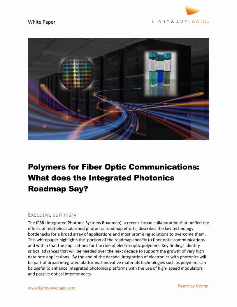
White Paper
www.lightwavelogic.com Faster by Design
Polymers for Fiber Optic Communications: What does the Integrated Photonics Roadmap Say?
Executive summary The IPSR (Integrated Photonic Systems Roadmap), a recent broad collaboration that unified the efforts of multiple established photonics roadmap efforts, describes the key technology bottlenecks for a broad array of applications and most promising solutions to overcome them. This whitepaper highlights the portion of the roadmap specific to fiber optic communications and within that the implications for the role of electro-optic polymers. Key findings identify critical advances that will be needed over the next decade to support the growth of very high data rate applications. By the end of the decade, integration of electronics with photonics will be part of broad integrated platforms. Innovative materials technologies such as polymers can be useful to enhance integrated photonics platforms with the use of high- speed modulators and passive optical interconnects.
Polymers in Integrated Photonics Roadmap
2
How do technology roadmaps help the industry? Technology roadmaps are critical for high-tech industries to align the continued progress of complex eco-systems of suppliers. They convey where the industry foresees challenges as well as what benchmarks technology platforms need to achieve to become and maintain their competitive advantage in fiber communications. The best-known example may be the ITRS (International Technology Roadmap for Semiconductors) which has guided the chip industry since 1998 through multiple generations of Moore’s Law advances with coordinated advances of lithography, process, design, etc., and is still very much in use by major semiconductor companies and stakeholders today.
The photonics industry similarly has over the past 4 decades generated a number of technology roadmaps to review and forecast trends in photonics. One of the rules of engagement for these working groups, which by definition must include competitors as well as collaborators, is a focus on pre-competitive technology trends rather than product developments. Nonetheless, the breadth of photonics is such that each roadmap has been application specific. The full IPSR1 (International Photonic Systems Roadmap) spans multiple photonics market segments including automotive, sensing, industrial IoT, medical, etc.
One of the most popular technology of these segment roadmaps has been for application to Datacenter Telecom, in other words fiber optic communications — an application with an especially critical need for roadmaps since data rates have progressed and inexorably much as Moore’s Law semiconductor capabilities have. (As a datapoint, the 1990 roadmap forecasted data rate speed increasing to the then dizzying rate of 1Gbps. Today, data rates are pushing deep into the Tbps range, or 1000x faster, as roadmaps look out towards 2030 and beyond.) The remainder of this whitepaper is specific to the Datacenter Telecom or fiber optic communications portion of the IPSR.
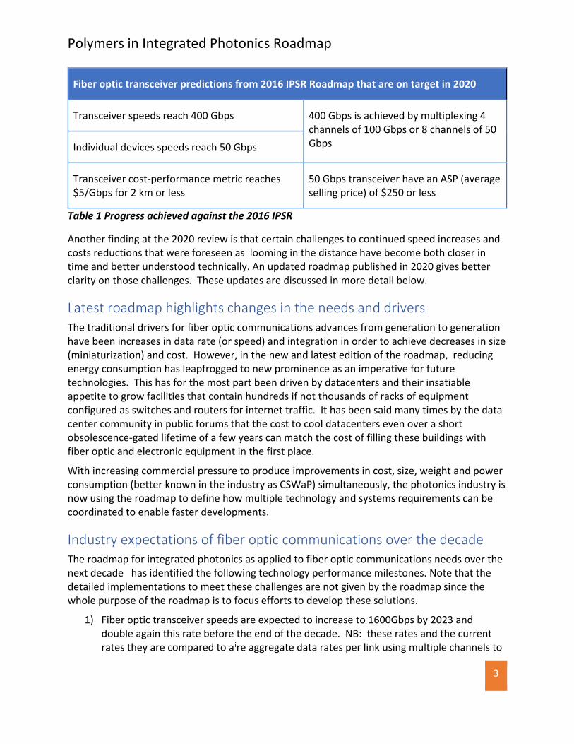
Roadmap updates assess progress in both speed and direction A major industry roadmap is typically updated every decade. However, for a fast growth important market such as integrated photonics a more frequent time scale is needed, perhaps bi-annually. One of the key exercises in road-mapping is to examine whether the prior roadmap predictions for the elapsed time have panned out. Did some milestones happen faster or slower than predicted? Did some new technology replace something? Another is to examine whether the drivers and therefore the future roadmap direction have changed. The IPSR roadmap forecast period is a decade, and the prior edition published in 2016 encompassed a view out to 2026. By 2020 it was already possible to have a mid-course checkpoint at which time it was found that the industry was indeed tracking to the 2016 forecast. Three specific predictions realized as noted Table 1 confirmed that the industry continues to move very quickly to ever higher speeds and lower costs.
1 The complete IPSR document can be found at https://aimphotonics.academy/roadmap/ipsr-roadmap
Polymers in Integrated Photonics Roadmap
3
Fiber optic transceiver predictions from 2016 IPSR Roadmap that are on target in 2020
Transceiver speeds reach 400 Gbps 400 Gbps is achieved by multiplexing 4 channels of 100 Gbps or 8 channels of 50 Gbps Individual devices speeds reach 50 Gbps
Transceiver cost-performance metric reaches $5/Gbps for 2 km or less
50 Gbps transceiver have an ASP (average selling price) of $250 or less
Table 1 Progress achieved against the 2016 IPSR
Another finding at the 2020 review is that certain challenges to continued speed increases and costs reductions that were foreseen as looming in the distance have become both closer in time and better understood technically. An updated roadmap published in 2020 gives better clarity on those challenges. These updates are discussed in more detail below.
Latest roadmap highlights changes in the needs and drivers The traditional drivers for fiber optic communications advances from generation to generation have been increases in data rate (or speed) and integration in order to achieve decreases in size (miniaturization) and cost. However, in the new and latest edition of the roadmap, reducing energy consumption has leapfrogged to new prominence as an imperative for future technologies. This has for the most part been driven by datacenters and their insatiable appetite to grow facilities that contain hundreds if not thousands of racks of equipment configured as switches and routers for internet traffic. It has been said many times by the data center community in public forums that the cost to cool datacenters even over a short obsolescence-gated lifetime of a few years can match the cost of filling these buildings with fiber optic and electronic equipment in the first place.
With increasing commercial pressure to produce improvements in cost, size, weight and power consumption (better known in the industry as CSWaP) simultaneously, the photonics industry is now using the roadmap to define how multiple technology and systems requirements can be coordinated to enable faster developments.
Industry expectations of fiber optic communications over the decade The roadmap for integrated photonics as applied to fiber optic communications needs over the next decade has identified the following technology performance milestones. Note that the detailed implementations to meet these challenges are not given by the roadmap since the whole purpose of the roadmap is to focus efforts to develop these solutions.
1) Fiber optic transceiver speeds are expected to increase to 1600Gbps by 2023 and double again this rate before the end of the decade. NB: these rates and the current rates they are compared to aire aggregate data rates per link using multiple channels to
Polymers in Integrated Photonics Roadmap
4
achieve these data-rates. The number of channels to achieve the goals is not specified by the roadmap.
2) Data rate densities will significantly increase from 25Tbps per rack unit (or 1U) today to levels approaching 2000Tbps (the roadmap forecasts 1600Tbps) by the end of the decade. While this represents a 400x increase, the roadmap does not suggest how these data rate densities will be able to pass through the face plate of routers and switches that can be found in data centers. It may well be that innovation over the next decade will enable technologies to achieve these challenges by 2030.
3) A cost performance metric of less than $1/Gbps is a challenging goal for integrated photonics that is expected to be achieved midway during the next decade.
4) Optical devices such as optical modulators are expected to be able to perform with analog 3dB optical bandwidths that exceed 70GHz (which using NRZ encoding of data is roughly equivalent to 100Gbps, or 200Gbps PAM4) early during the next decade. Performance expectations are forecasted to move in excess of 100GHz bandwidths by the end of the decade. An optical device with an analog 3dB optical bandwidth of 150GHz, similar to some of the best electro-optical polymer modulator devices already demonstrated, is roughly equivalent to 200Gbps NRZ and 300Gbps PAM4. This would represent by the end of the next decade device technologies that will be closing in on single channel operation for optical links.
5) Photonic integrated circuits (PICs) are forecasted to become hybrid. This means that pure play PIC platforms such as InP, GaAs, silicon photonics will be advanced to include a number of innovative and new technologies to reach the performance metrics that the industry would like to see. For example, electro-optic polymers can be added to InP or silicon photonics to update and improve the modulator performance. Silicon photonics is already use SiGe materials to so that the photodetectors can extend their long wavelength operation for telecom applications.
6) Low power consumption, less energy, more efficient operation are all metrics that not only are critical but essential for integrated photonics as the technology platforms advance over the next decade. The drive for lower power consumption is not expected to abate and it is expected that innovative solutions to simplify and reduce power consumption in both photonics and electronics will impact integrated photonics approaches in the next few years.
The next decade will demand more advanced optical device designs that can deal with thermal issues more effectively. Athermal device and optical designs will impact not only the device performance challenges, but also the engineering of package designs. Figuring solutions to eliminate coolers and temperature stages are techniques that could find routes to reduce cost structures, power consumption as well as higher data rate performance over the forecasted period.
Polymers in Integrated Photonics Roadmap
5
Polymers address the new imperatives of hybrid integration and decreased power consumption Polymer PIC technology encompasses both passive and active polymers. The roadmap notes both types of polymers are well positioned to meet the critical needs of the next decade. Passive polymers provide signal routing while active polymers are used to encode data. As electrical signaling struggles to cross circuit boards and package boundaries at the faster signal rates, passive polymer interconnects are making advances to fill the gap. Similarly, active polymer solutions are positioned to address gaps that are arising as semiconductors encounter intrinsic speed-power challenges.
Passive polymer interconnects include plastic optical fiber cabling, arrays of interconnect and planar structures. The variety reflects the application diversity that are met today with electrical interconnects and which may require optical versions in future. For example, as server speeds increasing to 100 Gbps there are active investigations underway to replace electrical Cat5/6/7 cable connecting servers with links of 10m or less to first-level switches with similarly low-cost and easy to deploy plastic optical fiber cables. At a smaller scale, chip interconnects have a similar dynamic with polymer wirebonds and even on-chip interconnects providing the optical equivalents of metal interconnects.
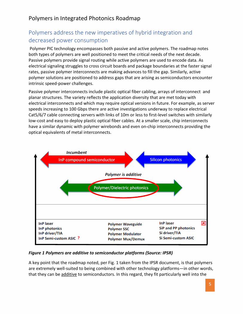
Figure 1 Polymers are additive to semiconductor platforms (Source: IPSR)
A key point that the roadmap noted, per Fig. 1 taken from the IPSR document, is that polymers are extremely well-suited to being combined with other technology platforms—in other words, that they can be additive to semiconductors. In this regard, they fit particularly well into the
Polymers in Integrated Photonics Roadmap
6
trends favoring hybrid integration. While there were debates a decade ago about the relative benefits of monolithic vs hybrid integration there is now a recognition that facing the challenges of the upcoming decade calls for combining the best available technologies. For example, silicon photonics foundries are almost universally adding SiN for reduced loss in passive structures. Active polymers additive to silicon photonics offer a speed boost to modulators and antennas compared to native silicon capabilities.
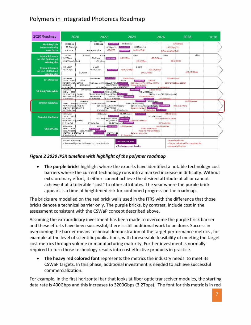
Reading the Roadmap Timeline The IPSR 2020 integrated photonics roadmap starts with a 2019 baseline and forecasts technology trends towards 2030 as shown in Figure 2 below . (See the Glossary for the many abbreviations used in the figure.) This is a complex figure that captures the multidimensional issues facing the industry as well as the timeline spanning a decade.
Before we look at the details of each row, note the difference in text types in each row moving from left to right over time.
• The black font depicts the progress for integrated photonics both desired and reasonably expected by the industry consensus in 2016 based on current trajectory.
Naturally, this outlook for technology development does not assume progress just magically happen by itself. The normal expectation is that the projected progress will require things like invention, innovation, dedicated funding etc. Identifying –and thereby enabling—these needs is a major value of the roadmap. But there is often a qualitative difference in the level of difficulty encountered at each stage as technologies advance past their “natural” capabilities. In the black font phase, the efforts are relatively low risk—i.e. “business as normal”.
Polymers in Integrated Photonics Roadmap
7
Figure 2 2020 IPSR timeline with highlight of the polymer roadmap
• The purple bricks highlight where the experts have identified a notable technology-cost barriers where the current technology runs into a marked increase in difficulty. Without extraordinary effort, it either cannot achieve the desired attribute at all or cannot achieve it at a tolerable “cost” to other attributes. The year where the purple brick appears is a time of heightened risk for continued progress on the roadmap.
The bricks are modelled on the red brick walls used in the ITRS with the difference that those bricks denote a technical barrier only. The purple bricks, by contrast, include cost in the assessment consistent with the CSWaP concept described above.
Assuming the extraordinary investment has been made to overcome the purple brick barrier and these efforts have been successful, there is still additional work to be done. Success in overcoming the barrier means technical demonstration of the target performance metrics , for example at the level of scientific publications, with foreseeable feasibility of meeting the target cost metrics through volume or manufacturing maturity. Further investment is normally required to turn those technology results into cost effective products in practice.
• The heavy red colored font represents the metrics the industry needs to meet its CSWaP targets. In this phase, additional investment is needed to achieve successful commercialization.
For example, in the first horizontal bar that looks at fiber optic transceiver modules, the starting data rate is 400Gbps and this increases to 3200Gbps (3.2Tbps). The font for this metric is in red
Polymers in Integrated Photonics Roadmap
8
which indicates that there will need to be major industry efforts to commercial this level of performance over the next decade. In the 2nd horizontal bar below, by 2024 the industry is wishing that 2km optical links to achieve a cost performance metric of less than 50c per Gbps, and the roadmap forecasts that $0.5/Gbps will be achieved by 2024 as indicated by the line below in red font. Both of these metrics are past the purple brick wall (or technology cost barrier), which indicates that the normal progression of technology advancement will need to be addressed as it may not achieve the $0.5/Gbps challenge as requested by the industry in 2023.
The rows are segmented into three groups.
1) Module metrics (first horizontal bar): Fiber optic communication transceiver modules where metrics of data rate, density and form factor are detailed. Note that density is given in units of Tbps/1U where U denotes a standard “rack unit” (see the Glossary).
2) Fiber optic link application as measured in typical link reach (second and third horizontal bars): Both rows are for the highest volume datacenter applications described technically in terms of the reach. The application for row 2 is the datacenter backbone which connects across a single large datacenter or datacenter campus. The application for row3 is the even higher volume intra-row connection within a datacenter. The key metrics of cost performance in these rows are in ($/Gbps). Two values are given at each time: the industry wish is the target that customers would like to pay for fiber optic transceivers in an optical link, while the industry plan is the typically higher price based on what suppliers are confident their costs can support.
3) Device technology segmented by material system (third to eighth horizontal bars) that will be utilized as part of the integrated photonics platform. These are listed as
a. InP monolithic: only InP and closely related compound semiconductor materials typically for lasers, detectors and other devices operating in the 1300 – 1600 nm wavelength range.
b. SiP and InP/SiGe hybrid: a combination of Silicon photonics and Indium Phosphide used together in an integrated photonics platform typically in the 1300 – 1600 nm range. The use of SiGe means that within the silicon photonics platform, the use of Silicon Germanium for longer wavelength receiving functions is expected. It is expected other materials such as InP and GaAs will be utilized with silicon over the forecast period.
c. Polymer Photonics: electro-optic polymers utilized both as a stand-alone technology platform such as modulators as well as polymers being added to another platform such as silicon photonics and/or indium phosphide typically in the 1300 – 1600 nm range.
d. Dielectric Photonics: In the silicon photonic platform the use of dielectric materials such as oxides and nitrides for on-board waveguides and other passive optic functions (WDM multiplexors, arrayed waveguide gratings (AWG) etc.),
Polymers in Integrated Photonics Roadmap
9
typically within the broader silicon photonics platform approach but can be over a broad wavelength range.
e. GaAs (VCSEL): Gallium Arsenide that is a compound semiconductor material that can be fabricated into semiconductor diode lasers where the device structure type is composed of a vertical cavity (hence the name vertical cavity surface emitting laser). These lasers are popular for short wavelengths where short optical links are used in the 800-1000nm wavelength range.
For all the different material systems in rows 3 - 8 , the challenge is to increase individual device speeds while also increasing the level of device integration. The first metric is # of devices integrated per photonic integrated circuit (PIC). For example, by 2021, polymer photonics is expected to be utilized with photonic integration densities of at least 10 devices (today we see multiples of 4: 4, 8, 16 etc.), and by the end of the decade the complexity is expected to reach device densities of around 10,000.2
The next metric is the per-device speed, expressed in terms of the analog optical 3dB bandwidth in GHz of the individual device such as a modulator. Polymer photonics modulators achieve 70GHz 3dB optical analog bandwidths already and are on their way to 100 GHz shortly.
The metric below the speed is the modulation scheme or format for encoding data that will be used. (For definitions of NRZ and PAM-n please see the Glossary.) In general, the modulation schemes become more complex as reflected partially in the increasing numerical values from PAM-4 to PAM-16. For a given data rates such as 100 Gbps, NRZ encoding requires the fastest analog device speed (e.g. 70GHz) while increasing levels of PAM-n trade off raw speed requirements for low noise, linearity and signal processing complexity. Coherent is a more complex class of modulation schemes that are well-established for telecom applications and are expected to trickle-down to datacenter applications during the forecast window,
The final metric in the Platforms row is wafer size. Increasing wafer sizes typically provide economies of scale and support higher levels of integration. Wafer sizes are expected to increase with the silicon photonics-based technologies similar to the trends seen in the electronic integrated circuit industry. With compound semiconductors such as InP, the trend to larger format wafers continues with efforts to increase sizes beyond 150mm. A number of R&D efforts are looking at 200mm InP but this has not been commercialized to date. With GaAs, 200mm format wafers are available even though their cost structure is high. Smaller wafer format fabrication plants that were on 3” and 4” format silicon wafers have now been replaced by 6” (150mm) and 8” (200mm) platforms. Larger silicon fabrication plants are now utilizing 12” (300mm) format silicon wafers, and the trend to 15” (450mm) format wafers is underway.
2 This in essence is similar to the original silicon semiconductor roadmaps where integration density progressed in the 1960’s and 1970’s from 100 transistors on chip which was called SSI (Small Scale Integration), to MSI (Medium Scale Integration), to more modern metrics such as ULSI (Ultra Large Scale Integration) where more than 1 million transistors are integrated onto a chip
Polymers in Integrated Photonics Roadmap
10
With the exception of Monolithic InP (Row 3) and GaAs (Row 8), all the materials approaches under active consideration today are Hybrid PIC. Hybrid technologies are gaining traction as pure play technologies tend not to be able to achieve all of the metrics needed by the industry. The movement towards mixing and matching materials and technologies will continue over the next decade.
Takeaways from the Roadmap for Polymers Comparing the materials rows, we see that the polymer photonics technology platform has the purple brick further out in in time (positioned more to the right of the roadmap) than the other technology platforms. This is due to the fact that electro-optic polymer devices intrinsically operate much faster, and with lower power consumption than the semiconductor equivalents. Conversely stated, non-polymer technologies reach the barriers sooner or at more risk to achieve the metrics needed for the integrated photonics fiber communications industry .
Specifically, this means that for the applications circled in red in the top row, namely 800Gbps- 1600Gbps module capacity and 100Tbps/1U density, polymers do not require fundamental additional invention to achieve these speeds with the requisite power and other attributes. Designing optical devices beyond 70GHz analog optical 3dB bandwidth will be a challenge for all optical devices in the industry, however, electro-optic polymers not only are expected to reach these goals first but are expected to lead the industry in performance by the end of the decade.
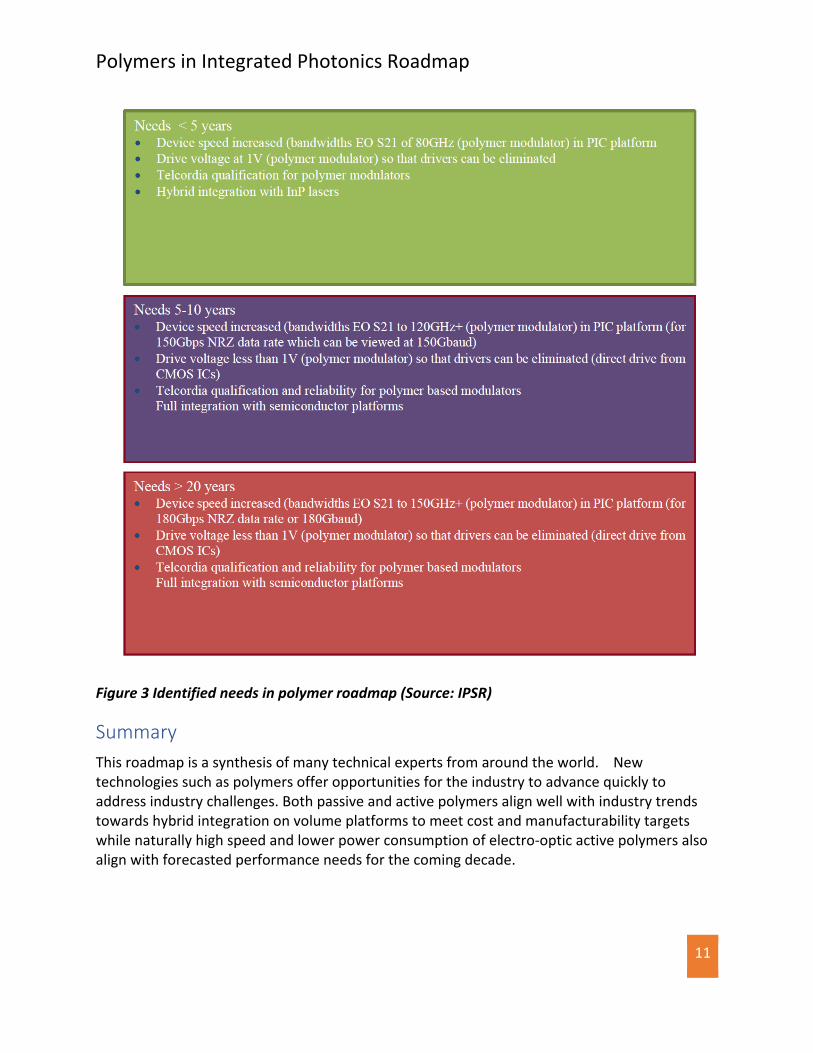
The roadmap document also lays out some upcoming goals specific to polymers as summarized in Figure 3. One focus area is standardization including material-specific test and measurement techniques as well as Telcordia qualification. The importance of integration with other PIC platforms has already been discussed.
Polymers in Integrated Photonics Roadmap
11
Figure 3 Identified needs in polymer roadmap (Source: IPSR)
Summary This roadmap is a synthesis of many technical experts from around the world. New technologies such as polymers offer opportunities for the industry to advance quickly to address industry challenges. Both passive and active polymers align well with industry trends towards hybrid integration on volume platforms to meet cost and manufacturability targets while naturally high speed and lower power consumption of electro-optic active polymers also align with forecasted performance needs for the coming decade.
Polymers in Integrated Photonics Roadmap
12
Glossary Definitions below are provided as an aid to understanding the IPSR figure and this whitepaper. As such, only the portion of the definition specific to this context is included.
$/Gbps: fiber optic transceiver module price scaled to its data capacity, e.g. a 100Gbps module selling for $100 meets a target metric of $1/Gbps
1U: 1 rack unit, sometimes also called 1RU. A unit of size for datacenter equipment typically stacked in racks. A standard rack is 19” wide, a single RU is 1.75” high. (A common fiber optics switch size called a “pizzabox” is 1 RU x 19”.)
3” wafer/fab: Size of semiconductor wafers as measured by their diameter, also the associate facilities and processes required to fabricate such wafers. NB:“/” here means “or”, not “per”.
ASIC: Application specific integrated circuit, a term widely used in electronics, now also applied to photonics in the context of OEIC ASIC or PIC ASIC.
Client-side: the side of a network architecture facing the less aggregated side of a switch, i.e. the servers or the end users. The counterpart is line-side. Typically, data rates, reaches and prices are lower on the client-side than the line-side.
CoB: Chip-on-board, a well-known minimalist electronic packaging style which typically gets applied for cost-reduction. For photonics, has been applied only to high-volume, lower-performance products previously but is now expected to move into higher-performance applications.
Coherent: A complex but very powerful modulation scheme historically used for long-haul telecom that is now trickling down to shorter reach applications, e.g. coherent client-side. Typically relies on powerful but expensive and power-hungry signal processing (DSP), hence coherent DSP-less is a desired improvement.
CP or Co-Pkg: Co-packaged optics, referring to a new direction where optics must be placed very close to big electronic switching or processor chips due to electrical interface limitations. Viewed by some as the next step after OBO. NB: this does not refer to the placement of both electronics and optics within a module.
Device: in photonics as in electronics, a device is a structure that performs a specific function. Multiple devices are combined to make integrated circuits. Examples of photonic devices are lasers, modulators, detectors, etc.
Dielectric: non-conductive, non-semiconductive materials such as oxides or nitrides typically used in the semiconductor industry as insulators, but here also used for optical devices.
DSP: Digital signal processing, a broad category of electronic function, here specifically referring to electronic signal conditioning at the transmitter or receiver end of a link to counter physical limitations of optical device performance.
DSP-less: Small transceiver printed circuit board where there is no DSP chip implemented. Attractive due to elimination of the cost and power consumption of the DSP chip.
Polymers in Integrated Photonics Roadmap
13
GaAs: Gallium Arsenide, a semiconductor material. Here, used as shorthand for the GaAs-based semiconductor technology used to make devices.
Gbps: Gigabits per second, 109 bits per second (1Gbps is equivalent to 1000Mbps)
GHz: GigaHertz, a measurement in frequency, used to characterize component speed.
InP: Indium Phosphide, a semiconductor material. Here, used as shorthand for the InP-based semiconductor technology used to make devices.
Int Driver: Integrated driver, a type of electronic device that is part of a fiber optic transmitter function. Specifically, a version where the driver function is integrated with other functions on the chip rather than as a separate chip.
km: kilometers, length of nominal communications link reach used to categorize fiber optic transceiver products. Some common standard types are 100m, 2 km, 10 km, etc.
m: meters, length of nominal communications link reach used to categorize fiber optic transceiver products. Some common standard types are 100m, 2 km, 10 km, etc.
Micro Co-Pkg: A more miniaturized version of a co-packaged solution
Modulation Scheme: the way data is represented or encoded onto the optical signal, for example in an NRZ scheme a high power may represent a “1” bit value while a low power may represent a “0” bit value.
Module: Fiber optic transceiver, specifically the physical package which is typically a small metal housing with electrical and optical connectors. It contains a small circuit board on which are soldered multiple electronic IC (integrated circuits) and PIC (photonic integrated circuit) packaged chips. Today the vast majority are pluggable into the front panel of a server or switch chassis, after which fiber optic cables are plugged into the module.
NRZ: Non-return-to-zero, a data format with simple encoding in which a “1” bit is typically a high level and a “0” bit is a low level.
OBO: On-board optics, referring to a module type placed directly onto a system printed circuit board at time of manufacture. An alternative to pluggable transceivers receiving increased interest lately due to concerns about lack of space on the front panel due to inadequate module density.
OEIC or OEIC ASIC: Optoelectronic Integrated Circuit ASIC, an integrated chip with multiple optoelectronics devices. Strictly, an OEIC has electronics fully integrated into the chip with the photonics as distinct from PICs which historically are only photonic.
OSFP: (Octal Small Formfactor Pluggable), a de facto standardized module type, where octal denotes that eight high-speed electrical interfaces are supported. NB: the number of optical channels supported by the module is not necessarily the same as the number of electrical interfaces, e.g. a common version implements a total module capacity of 400Gbps using 8 x 50 Gbps on the electrical side with 4 x 100Gbps on the optical side.
Polymers in Integrated Photonics Roadmap
14
QSFP: Quad Small Formfactor Pluggable, a standard module type, where quad denotes that four high-speed electrical interfaces are supported, e.g. 4 x 25 Gbps for a total module capacity of 100 Gbps or 4 x 100Gbps for a total module capacity of 400Gbps. NB: the number of optical channels supported by the module is not necessarily the same as the number of electrical interfaces.
PAM4/PAM8/PAM16: Pulse Amplitude Modulation with 4, 8 or 16 levels, multi-level data encoding that trade off more data capacity at the cost of more complexity. E.g. PAM4 typically doubles the data rate compared to NRZ encoding. Also sometimes written as PAM-4. etc.
PIC: Photonics Integrated Circuit, an integrated chip with multiple photonics devices. Historically, the term referred to a chip with photonic devices only. Today the term is also used to include chips with both photonic and electronic devices integrated together, particularly in the usage PIC ASIC.
Rx: Shorthand for fiber optic receiver.
SiP: Silicon photonics
Tbps: Terabits per second, 1012 bits per second (1Tbps is equivalent to 1000Gbps).
TIA: Transimpedance amplifier, a type of electronic device that is part of a fiber optic receiver function.
Tx: Shorthand for fiber optic transmitter
TxRx: Shorthand for fiber optic transceiver, denoting that both transmit and receive functions are included.
VCSEL: Vertical cavity surface emitting laser, typically used in data communication modules for links of 100m or shorter.
WDM: Wavelength Division Multiplexing, a technique for combining multiple optical signals into the same fiber to increase the data carrying capacity of the link.
About Lightwave Logic, Inc. Lightwave Logic, Inc. (OTCQB: LWLG) is developing a platform leveraging its proprietary engineered electro-optic (EO) polymers to transmit data at higher speeds with less power. The Company's high-activity and high-stability organic polymers allow Lightwave Logic to create next-generation photonic EO devices, which convert data from electrical signals into optical signals, for applications in data communications and telecommunications markets. For more information, please visit www.lightwavelogic.com or contact us at [email protected] ©2021 Lightwave Logic, Inc.