Embed Size (px)
Citation preview
http://www.diva-portal.org
Postprint
This is the accepted version of a paper published in IEEE Transactions on Electron Devices. Thispaper has been peer-reviewed but does not include the final publisher proof-corrections or journalpagination.
Citation for the original published paper (version of record):
Lanni, L., Ghandi, R., Malm, B G., Zetterling, C-M. (2012)Design and Characterization of High-Temperature ECL-Based Bipolar Integrated Circuits in4H-SiC.IEEE Transactions on Electron Devices, 59(4): 1076-1083http://dx.doi.org/10.1109/TED.2011.2182514
Access to the published version may require subscription.
N.B. When citing this work, cite the original published paper.
© 2012 IEEE. Personal use of this material is permitted. Permission from IEEE must be obtainedfor all other uses, in any current or future media, including reprinting/republishing this material foradvertising or promotional purposes, creating new collective works, for resale or redistribution toservers or lists, or reuse of any copyrighted component of this work in other works.
Permanent link to this version:http://urn.kb.se/resolve?urn=urn:nbn:se:kth:diva-72233
Design and Characterization of High-TemperatureECL-Based Bipolar Integrated Circuits in 4H-SiC
Luigia Lanni, Reza Ghandi, Bengt Gunnar Malm, Senior Member, IEEE,Carl-Mikael Zetterling, Senior Member, IEEE, and Mikael Östling, Fellow, IEEE
Abstract—Operation up to 300 ◦C of low-voltage 4H-SiCn-p-n bipolar transistors and digital integrated circuits based onemitter-coupled logic is demonstrated. Stable noise margins ofabout 1 V are reported for a two-input OR–NOR gate operatedon −15 V supply voltage from 27 ◦C up to 300 ◦C. In the sametemperature range, an oscillation frequency of about 2 MHz is alsoreported for a three-stage ring oscillator.
Index Terms—Bipolar junction transistor (BJT), emitter cou-pled logic (ECL), high-temperature integrated circuits (ICs),OR–NOR gate, silicon carbide (SiC).
I. INTRODUCTION
S ILICON CARBIDE (SiC) is a wide band-gap semiconduc-tor that provides significant advantages for high-power and
high-temperature applications because of its high critical field strength and thermal conductivity [1]. In particular, SiC devices are suitable for high-temperature integrated circuits (ICs) due to their capability to work at high temperature and relaxed cooling requirements.
High-temperature operation of ICs has been already reported in SiC with different devices and logics. Long-term stability of JFET ICs, both analog and digital, has been demonstrated in 6H-SiC with circuit operation at 500 ◦C for thousand hours [2]. CMOS technology has been investigated since early 1990s in 6H-SiC [3] and has been recently reported in 4H-SiC [4]. In both cases, 300 ◦C operation of digital circuits has been shown. Bipolar ICs have been also demonstrated in 4H-SiC with operation of up to 355 ◦C of transistor–transistor logic (TTL) and propagation delays comparable with those of silicon TTL circuits (∼10 ns) [5].
In this paper, we report a bipolar IC technology in 4H-SiC based on emitter-coupled logic (ECL) with transistor current gain of about 45 at room temperature, which is capable of operation at 300 ◦C. The ECL permits a wide operating range both in terms of temperature and supply voltage since it is based on differential stages and allows an easy implementation of a temperature and supply voltage compensation network. The goal of this first paper is to demonstrate high-temperature
Manuscript received November 1, 2011; revised December 22, 2011; accepted December 27, 2011. Date of publication February 10, 2012; date of current version March 23, 2012. The review of this paper was arranged by Editor J. D. Cressler.
The authors are with the School of Information and Communication Technol-ogy, KTH Royal Institute of Technology, 164 40 Stockholm, Sweden (e-mail: [email protected]) .
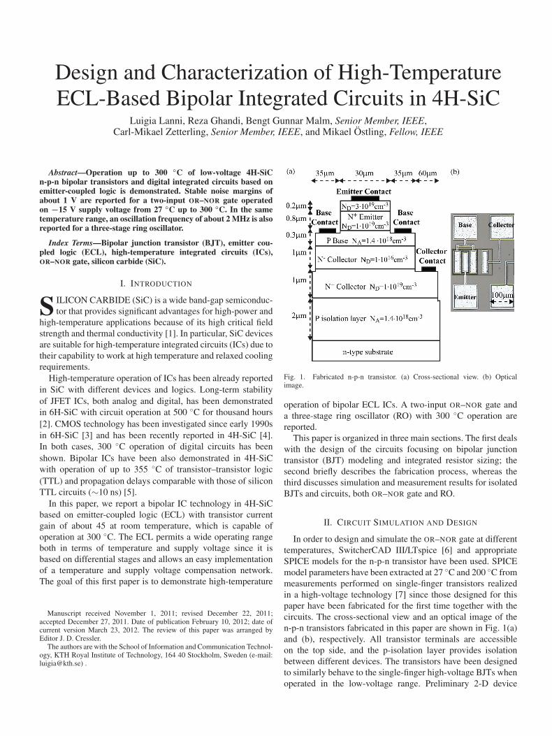
Fig. 1. Fabricated n-p-n transistor. (a) Cross-sectional view. (b) Opticalimage.
operation of bipolar ECL ICs. A two-input OR–NOR gate anda three-stage ring oscillator (RO) with 300 ◦C operation arereported.
This paper is organized in three main sections. The first dealswith the design of the circuits focusing on bipolar junctiontransistor (BJT) modeling and integrated resistor sizing; thesecond briefly describes the fabrication process, whereas thethird discusses simulation and measurement results for isolatedBJTs and circuits, both OR–NOR gate and RO.
II. CIRCUIT SIMULATION AND DESIGN
In order to design and simulate the OR–NOR gate at differenttemperatures, SwitcherCAD III/LTspice [6] and appropriateSPICE models for the n-p-n transistor have been used. SPICEmodel parameters have been extracted at 27 ◦C and 200 ◦C frommeasurements performed on single-finger transistors realizedin a high-voltage technology [7] since those designed for thispaper have been fabricated for the first time together with thecircuits. The cross-sectional view and an optical image of then-p-n transistors fabricated in this paper are shown in Fig. 1(a)and (b), respectively. All transistor terminals are accessibleon the top side, and the p-isolation layer provides isolationbetween different devices. The transistors have been designedto similarly behave to the single-finger high-voltage BJTs whenoperated in the low-voltage range. Preliminary 2-D device
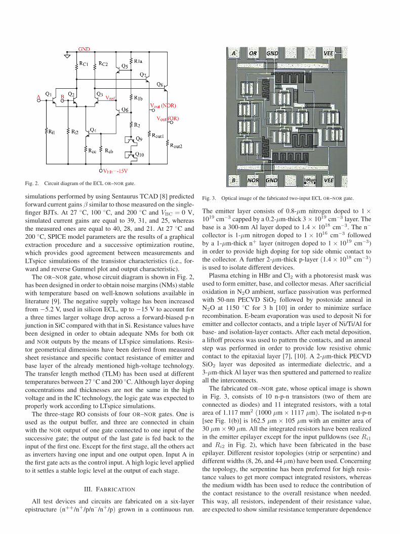
Fig. 2. Circuit diagram of the ECL OR–NOR gate.
simulations performed by using Sentaurus TCAD [8] predictedforward current gains β similar to those measured on the single-finger BJTs. At 27 ◦C, 100 ◦C, and 200 ◦C and VBC = 0 V,simulated current gains are equal to 39, 31, and 25, whereasthe measured ones are equal to 40, 28, and 21. At 27 ◦C and200 ◦C, SPICE model parameters are the results of a graphicalextraction procedure and a successive optimization routine,which provides good agreement between measurements andLTspice simulations of the transistor characteristics (i.e., for-ward and reverse Gummel plot and output characteristic).
The OR–NOR gate, whose circuit diagram is shown in Fig. 2,has been designed in order to obtain noise margins (NMs) stablewith temperature based on well-known solutions available inliterature [9]. The negative supply voltage has been increasedfrom −5.2 V, used in silicon ECL, up to −15 V to account fora three times larger voltage drop across a forward-biased p-njunction in SiC compared with that in Si. Resistance values havebeen designed in order to obtain adequate NMs for both OR
and NOR outputs by the means of LTspice simulations. Resis-tor geometrical dimensions have been derived from measuredsheet resistance and specific contact resistance of emitter andbase layer of the already mentioned high-voltage technology.The transfer length method (TLM) has been used at differenttemperatures between 27 ◦C and 200 ◦C. Although layer dopingconcentrations and thicknesses are not the same in the highvoltage and in the IC technology, the logic gate was expected toproperly work according to LTspice simulations.
The three-stage RO consists of four OR–NOR gates. One isused as the output buffer, and three are connected in chainwith the NOR output of one gate connected to one input of thesuccessive gate; the output of the last gate is fed back to theinput of the first one. Except for the first stage, all the others actas inverters having one input and one output open. Input A inthe first gate acts as the control input. A high logic level appliedto it settles a stable logic level at the output of each stage.
III. FABRICATION
All test devices and circuits are fabricated on a six-layerepistructure (n++/n+/p/n−/n+/p) grown in a continuous run.
Fig. 3. Optical image of the fabricated two-input ECL OR–NOR gate.
The emitter layer consists of 0.8-μm nitrogen doped to 1 ×1019 cm−3 capped by a 0.2-μm-thick 3 × 1019 cm−3 layer. Thebase is a 300-nm Al layer doped to 1.4 × 1018 cm−3. The n−
collector is 1-μm nitrogen doped to 1 × 1016 cm−3 followedby a 1-μm-thick n+ layer (nitrogen doped to 1 × 1019 cm−3)in order to provide high doping for top side ohmic contact tothe collector. A further 2-μm-thick p-layer (1.4 × 1018 cm−3)is used to isolate different devices.
Plasma etching in HBr and Cl2 with a photoresist mask wasused to form emitter, base, and collector mesas. After sacrificialoxidation in N2O ambient, surface passivation was performedwith 50-nm PECVD SiO2 followed by postoxide anneal inN2O at 1150 ◦C for 3 h [10] in order to minimize surfacerecombination. E-beam evaporation was used to deposit Ni foremitter and collector contacts, and a triple layer of Ni/Ti/Al forbase- and isolation-layer contacts. After each metal deposition,a liftoff process was used to pattern the contacts, and an annealstep was performed in order to provide low resistive ohmiccontact to the epitaxial layer [7], [10]. A 2-μm-thick PECVDSiO2 layer was deposited as intermediate dielectric, and a3-μm-thick Al layer was then sputtered and patterned to realizeall the interconnects.
The fabricated OR–NOR gate, whose optical image is shownin Fig. 3, consists of 10 n-p-n transistors (two of them areconnected as diodes) and 11 integrated resistors, with a totalarea of 1.117 mm2 (1000 μm × 1117 μm). The isolated n-p-n[see Fig. 1(b)] is 162.5 μm × 105 μm with an emitter area of30 μm × 90 μm. All the integrated resistors have been realizedin the emitter epilayer except for the input pulldowns (see Ri1
and Ri2 in Fig. 2), which have been fabricated in the baseepilayer. Different resistor topologies (strip or serpentine) anddifferent widths (8, 26, and 44 μm) have been used. Concerningthe topology, the serpentine has been preferred for high resis-tance values to get more compact integrated resistors, whereasthe medium width has been used to reduce the contribution ofthe contact resistance to the overall resistance when needed.This way, all resistors, independent of their resistance value,are expected to show similar resistance temperature dependence
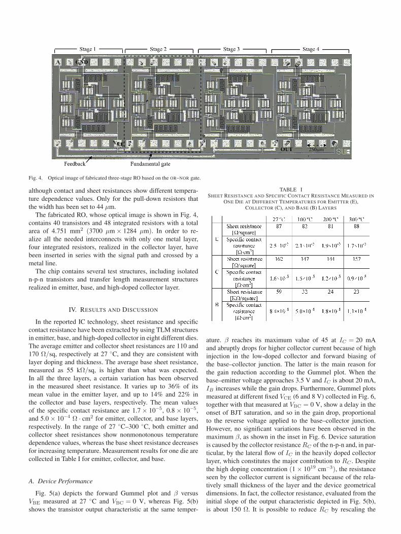
Fig. 4. Optical image of fabricated three-stage RO based on the OR–NOR gate.
although contact and sheet resistances show different tempera-ture dependence values. Only for the pull-down resistors thatthe width has been set to 44 μm.
The fabricated RO, whose optical image is shown in Fig. 4,contains 40 transistors and 48 integrated resistors with a totalarea of 4.751 mm2 (3700 μm × 1284 μm). In order to re-alize all the needed interconnects with only one metal layer,four integrated resistors, realized in the collector layer, havebeen inserted in series with the signal path and crossed by ametal line.
The chip contains several test structures, including isolatedn-p-n transistors and transfer length measurement structuresrealized in emitter, base, and high-doped collector layer.
IV. RESULTS AND DISCUSSION
In the reported IC technology, sheet resistance and specificcontact resistance have been extracted by using TLM structuresin emitter, base, and high-doped collector in eight different dies.The average emitter and collector sheet resistances are 110 and170 Ω/sq, respectively at 27 ◦C, and they are consistent withlayer doping and thickness. The average base sheet resistance,measured as 55 kΩ/sq, is higher than what was expected.In all the three layers, a certain variation has been observedin the measured sheet resistance. It varies up to 36% of itsmean value in the emitter layer, and up to 14% and 22% inthe collector and base layers, respectively. The mean valuesof the specific contact resistance are 1.7 × 10⁻⁵, 0.8 × 10⁻⁵,and 5.0 × 10⁻⁴ Ω · cm2 for emitter, collector, and base layers,respectively. In the range of 27 ◦C–300 ◦C, both emitter andcollector sheet resistances show nonmonotonous temperaturedependence values, whereas the base sheet resistance decreasesfor increasing temperature. Measurement results for one die arecollected in Table I for emitter, collector, and base.
A. Device Performance
Fig. 5(a) depicts the forward Gummel plot and β versusVBE measured at 27 ◦C and VBC = 0 V, whereas Fig. 5(b)shows the transistor output characteristic at the same temper-
TABLE ISHEET RESISTANCE AND SPECIFIC CONTACT RESISTANCE MEASURED IN
ONE DIE AT DIFFERENT TEMPERATURES FOR EMITTER (E),COLLECTOR (C), AND BASE (B) LAYERS
ature. β reaches its maximum value of 45 at IC = 20 mAand abruptly drops for higher collector current because of highinjection in the low-doped collector and forward biasing ofthe base–collector junction. The latter is the main reason forthe gain reduction according to the Gummel plot. When thebase–emitter voltage approaches 3.5 V and IC is about 20 mA,IB increases while the gain drops. Furthermore, Gummel plotsmeasured at different fixed VCE (6 and 8 V) collected in Fig. 6,together with that measured at VBC = 0 V, show a delay in theonset of BJT saturation, and so in the gain drop, proportionalto the reverse voltage applied to the base–collector junction.However, no significant variations have been observed in themaximum β, as shown in the inset in Fig. 6. Device saturationis caused by the collector resistance RC of the n-p-n and, in par-ticular, by the lateral flow of IC in the heavily doped collectorlayer, which constitutes the major contribution to RC . Despitethe high doping concentration (1 × 1019 cm−3), the resistanceseen by the collector current is significant because of the rela-tively small thickness of the layer and the device geometricaldimensions. In fact, the collector resistance, evaluated from theinitial slope of the output characteristic depicted in Fig. 5(b),is about 150 Ω. It is possible to reduce RC by rescaling the
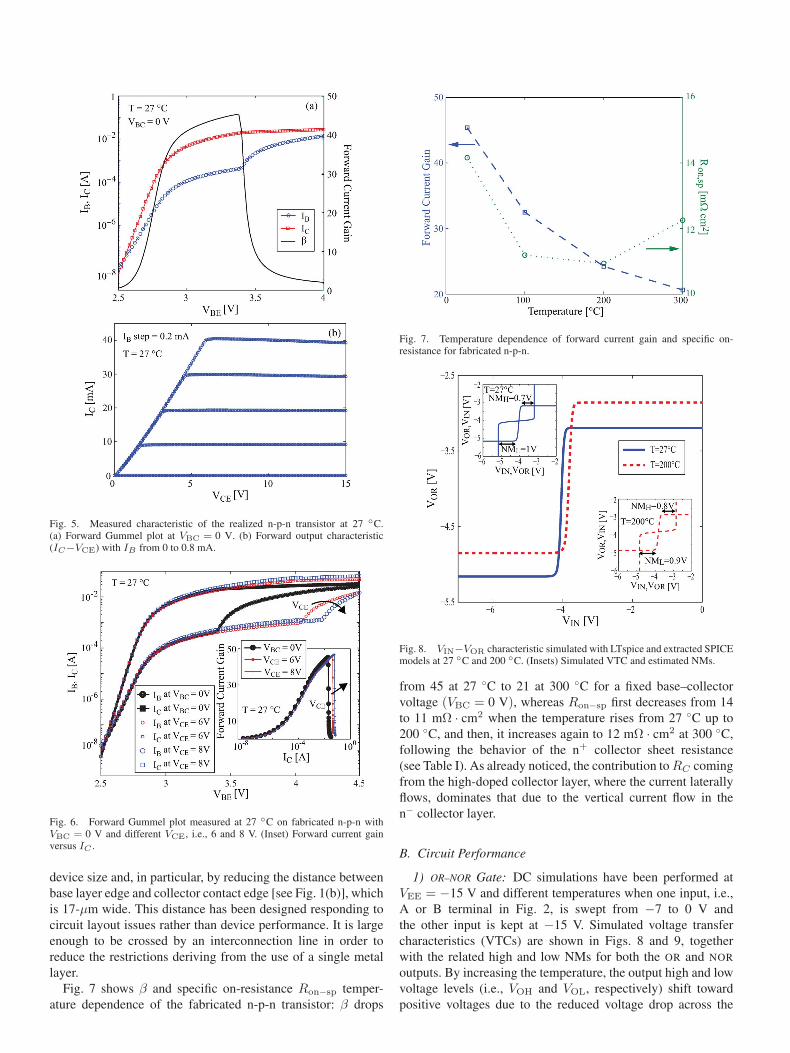
Fig. 5. Measured characteristic of the realized n-p-n transistor at 27 ◦C.(a) Forward Gummel plot at VBC = 0 V. (b) Forward output characteristic(IC−VCE) with IB from 0 to 0.8 mA.
Fig. 6. Forward Gummel plot measured at 27 ◦C on fabricated n-p-n withVBC = 0 V and different VCE, i.e., 6 and 8 V. (Inset) Forward current gainversus IC .
device size and, in particular, by reducing the distance betweenbase layer edge and collector contact edge [see Fig. 1(b)], whichis 17-μm wide. This distance has been designed responding tocircuit layout issues rather than device performance. It is largeenough to be crossed by an interconnection line in order toreduce the restrictions deriving from the use of a single metallayer.
Fig. 7 shows β and specific on-resistance Ron−sp temper-ature dependence of the fabricated n-p-n transistor: β drops
Fig. 7. Temperature dependence of forward current gain and specific on-resistance for fabricated n-p-n.
Fig. 8. VIN−VOR characteristic simulated with LTspice and extracted SPICEmodels at 27 ◦C and 200 ◦C. (Insets) Simulated VTC and estimated NMs.
from 45 at 27 ◦C to 21 at 300 ◦C for a fixed base–collectorvoltage (VBC = 0 V), whereas Ron−sp first decreases from 14to 11 mΩ · cm2 when the temperature rises from 27 ◦C up to200 ◦C, and then, it increases again to 12 mΩ · cm2 at 300 ◦C,following the behavior of the n+ collector sheet resistance(see Table I). As already noticed, the contribution to RC comingfrom the high-doped collector layer, where the current laterallyflows, dominates that due to the vertical current flow in then− collector layer.
B. Circuit Performance
1) OR–NOR Gate: DC simulations have been performed atVEE = −15 V and different temperatures when one input, i.e.,A or B terminal in Fig. 2, is swept from −7 to 0 V andthe other input is kept at −15 V. Simulated voltage transfercharacteristics (VTCs) are shown in Figs. 8 and 9, togetherwith the related high and low NMs for both the OR and NOR
outputs. By increasing the temperature, the output high and lowvoltage levels (i.e., VOH and VOL, respectively) shift towardpositive voltages due to the reduced voltage drop across the
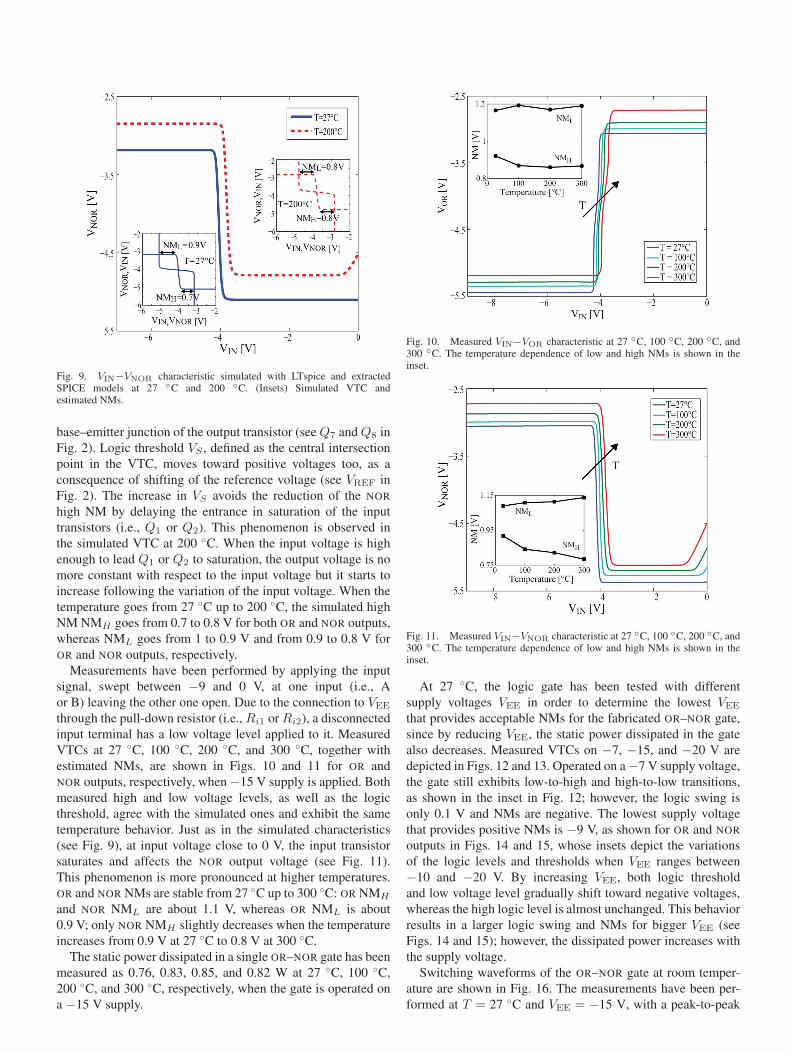
Fig. 9. VIN−VNOR characteristic simulated with LTspice and extractedSPICE models at 27 ◦C and 200 ◦C. (Insets) Simulated VTC andestimated NMs.
base–emitter junction of the output transistor (see Q7 and Q8 inFig. 2). Logic threshold VS , defined as the central intersectionpoint in the VTC, moves toward positive voltages too, as aconsequence of shifting of the reference voltage (see VREF inFig. 2). The increase in VS avoids the reduction of the NOR
high NM by delaying the entrance in saturation of the inputtransistors (i.e., Q1 or Q2). This phenomenon is observed inthe simulated VTC at 200 ◦C. When the input voltage is highenough to lead Q1 or Q2 to saturation, the output voltage is nomore constant with respect to the input voltage but it starts toincrease following the variation of the input voltage. When thetemperature goes from 27 ◦C up to 200 ◦C, the simulated highNM NMH goes from 0.7 to 0.8 V for both OR and NOR outputs,whereas NML goes from 1 to 0.9 V and from 0.9 to 0.8 V forOR and NOR outputs, respectively.
Measurements have been performed by applying the inputsignal, swept between −9 and 0 V, at one input (i.e., Aor B) leaving the other one open. Due to the connection to VEE
through the pull-down resistor (i.e., Ri1 or Ri2), a disconnectedinput terminal has a low voltage level applied to it. MeasuredVTCs at 27 ◦C, 100 ◦C, 200 ◦C, and 300 ◦C, together withestimated NMs, are shown in Figs. 10 and 11 for OR andNOR outputs, respectively, when −15 V supply is applied. Bothmeasured high and low voltage levels, as well as the logicthreshold, agree with the simulated ones and exhibit the sametemperature behavior. Just as in the simulated characteristics(see Fig. 9), at input voltage close to 0 V, the input transistorsaturates and affects the NOR output voltage (see Fig. 11).This phenomenon is more pronounced at higher temperatures.OR and NOR NMs are stable from 27 ◦C up to 300 ◦C: OR NMH
and NOR NML are about 1.1 V, whereas OR NML is about0.9 V; only NOR NMH slightly decreases when the temperatureincreases from 0.9 V at 27 ◦C to 0.8 V at 300 ◦C.
The static power dissipated in a single OR–NOR gate has beenmeasured as 0.76, 0.83, 0.85, and 0.82 W at 27 ◦C, 100 ◦C,200 ◦C, and 300 ◦C, respectively, when the gate is operated ona −15 V supply.
Fig. 10. Measured VIN−VOR characteristic at 27 ◦C, 100 ◦C, 200 ◦C, and300 ◦C. The temperature dependence of low and high NMs is shown in theinset.
Fig. 11. Measured VIN−VNOR characteristic at 27 ◦C, 100 ◦C, 200 ◦C, and300 ◦C. The temperature dependence of low and high NMs is shown in theinset.
At 27 ◦C, the logic gate has been tested with differentsupply voltages VEE in order to determine the lowest VEE
that provides acceptable NMs for the fabricated OR–NOR gate,since by reducing VEE, the static power dissipated in the gatealso decreases. Measured VTCs on −7, −15, and −20 V aredepicted in Figs. 12 and 13. Operated on a −7 V supply voltage,the gate still exhibits low-to-high and high-to-low transitions,as shown in the inset in Fig. 12; however, the logic swing isonly 0.1 V and NMs are negative. The lowest supply voltagethat provides positive NMs is −9 V, as shown for OR and NOR
outputs in Figs. 14 and 15, whose insets depict the variationsof the logic levels and thresholds when VEE ranges between−10 and −20 V. By increasing VEE, both logic thresholdand low voltage level gradually shift toward negative voltages,whereas the high logic level is almost unchanged. This behaviorresults in a larger logic swing and NMs for bigger VEE (seeFigs. 14 and 15); however, the dissipated power increases withthe supply voltage.
Switching waveforms of the OR–NOR gate at room temper-ature are shown in Fig. 16. The measurements have been per-formed at T = 27 ◦C and VEE = −15 V, with a peak-to-peak
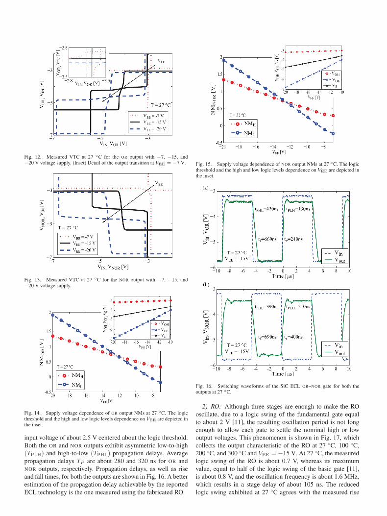
Fig. 12. Measured VTC at 27 ◦C for the OR output with −7, −15, and−20 V voltage supply. (Inset) Detail of the output transition at VEE = −7 V.
Fig. 13. Measured VTC at 27 ◦C for the NOR output with −7, −15, and−20 V voltage supply.
Fig. 14. Supply voltage dependence of OR output NMs at 27 ◦C. The logicthreshold and the high and low logic levels dependence on VEE are depicted inthe inset.
input voltage of about 2.5 V centered about the logic threshold.Both the OR and NOR outputs exhibit asymmetric low-to-high(TPLH) and high-to-low (TPHL) propagation delays. Averagepropagation delays TP are about 280 and 320 ns for OR andNOR outputs, respectively. Propagation delays, as well as riseand fall times, for both the outputs are shown in Fig. 16. A betterestimation of the propagation delay achievable by the reportedECL technology is the one measured using the fabricated RO.
Fig. 15. Supply voltage dependence of NOR output NMs at 27 ◦C. The logicthreshold and the high and low logic levels dependence on VEE are depicted inthe inset.
Fig. 16. Switching waveforms of the SiC ECL OR–NOR gate for both theoutputs at 27 ◦C.
2) RO: Although three stages are enough to make the ROoscillate, due to a logic swing of the fundamental gate equalto about 2 V [11], the resulting oscillation period is not longenough to allow each gate to settle the nominal high or lowoutput voltages. This phenomenon is shown in Fig. 17, whichcollects the output characteristic of the RO at 27 ◦C, 100 ◦C,200 ◦C, and 300 ◦C and VEE = −15 V. At 27 ◦C, the measuredlogic swing of the RO is about 0.7 V, whereas its maximumvalue, equal to half of the logic swing of the basic gate [11],is about 0.8 V, and the oscillation frequency is about 1.6 MHz,which results in a stage delay of about 105 ns. The reducedlogic swing exhibited at 27 ◦C agrees with the measured rise
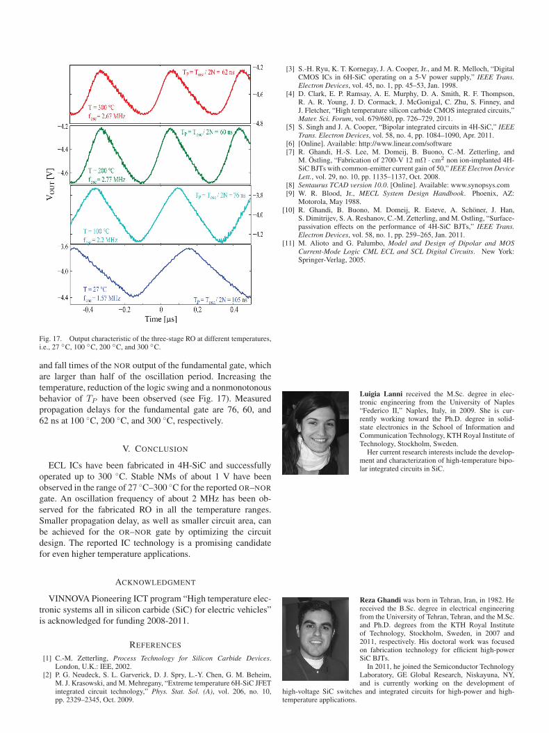
Fig. 17. Output characteristic of the three-stage RO at different temperatures,i.e., 27 ◦C, 100 ◦C, 200 ◦C, and 300 ◦C.
and fall times of the NOR output of the fundamental gate, whichare larger than half of the oscillation period. Increasing thetemperature, reduction of the logic swing and a nonmonotonousbehavior of TP have been observed (see Fig. 17). Measuredpropagation delays for the fundamental gate are 76, 60, and62 ns at 100 ◦C, 200 ◦C, and 300 ◦C, respectively.
V. CONCLUSION
ECL ICs have been fabricated in 4H-SiC and successfullyoperated up to 300 ◦C. Stable NMs of about 1 V have beenobserved in the range of 27 ◦C–300 ◦C for the reported OR–NOR
gate. An oscillation frequency of about 2 MHz has been ob-served for the fabricated RO in all the temperature ranges.Smaller propagation delay, as well as smaller circuit area, canbe achieved for the OR–NOR gate by optimizing the circuitdesign. The reported IC technology is a promising candidatefor even higher temperature applications.
ACKNOWLEDGMENT
VINNOVA Pioneering ICT program “High temperature elec-tronic systems all in silicon carbide (SiC) for electric vehicles”is acknowledged for funding 2008-2011.
REFERENCES
[1] C.-M. Zetterling, Process Technology for Silicon Carbide Devices.London, U.K.: IEE, 2002.
[2] P. G. Neudeck, S. L. Garverick, D. J. Spry, L.-Y. Chen, G. M. Beheim,M. J. Krasowski, and M. Mehregany, “Extreme temperature 6H-SiC JFETintegrated circuit technology,” Phys. Stat. Sol. (A), vol. 206, no. 10,pp. 2329–2345, Oct. 2009.
[3] S.-H. Ryu, K. T. Kornegay, J. A. Cooper, Jr., and M. R. Melloch, “DigitalCMOS ICs in 6H-SiC operating on a 5-V power supply,” IEEE Trans.Electron Devices, vol. 45, no. 1, pp. 45–53, Jan. 1998.
[4] D. Clark, E. P. Ramsay, A. E. Murphy, D. A. Smith, R. F. Thompson,R. A. R. Young, J. D. Cormack, J. McGonigal, C. Zhu, S. Finney, andJ. Fletcher, “High temperature silicon carbide CMOS integrated circuits,”Mater. Sci. Forum, vol. 679/680, pp. 726–729, 2011.
[5] S. Singh and J. A. Cooper, “Bipolar integrated circuits in 4H-SiC,” IEEETrans. Electron Devices, vol. 58, no. 4, pp. 1084–1090, Apr. 2011.
[6] [Online]. Available: http://www.linear.com/software[7] R. Ghandi, H.-S. Lee, M. Domeij, B. Buono, C.-M. Zetterling, and
M. Östling, “Fabrication of 2700-V 12 mΩ · cm2 non ion-implanted 4H-SiC BJTs with common-emitter current gain of 50,” IEEE Electron DeviceLett., vol. 29, no. 10, pp. 1135–1137, Oct. 2008.
[8] Sentaurus TCAD version 10.0. [Online]. Available: www.synopsys.com[9] W. R. Blood, Jr., MECL System Design Handbook. Phoenix, AZ:
Motorola, May 1988.[10] R. Ghandi, B. Buono, M. Domeij, R. Esteve, A. Schöner, J. Han,
S. Dimitrijev, S. A. Reshanov, C.-M. Zetterling, and M. Ostling, “Surface-passivation effects on the performance of 4H-SiC BJTs,” IEEE Trans.Electron Devices, vol. 58, no. 1, pp. 259–265, Jan. 2011.
[11] M. Alioto and G. Palumbo, Model and Design of Dipolar and MOSCurrent-Mode Logic CML ECL and SCL Digital Circuits. New York:Springer-Verlag, 2005.
Luigia Lanni received the M.Sc. degree in elec-tronic engineering from the University of Naples“Federico II,” Naples, Italy, in 2009. She is cur-rently working toward the Ph.D. degree in solid-state electronics in the School of Information andCommunication Technology, KTH Royal Institute ofTechnology, Stockholm, Sweden.
Her current research interests include the develop-ment and characterization of high-temperature bipo-lar integrated circuits in SiC.
Reza Ghandi was born in Tehran, Iran, in 1982. Hereceived the B.Sc. degree in electrical engineeringfrom the University of Tehran, Tehran, and the M.Sc.and Ph.D. degrees from the KTH Royal Instituteof Technology, Stockholm, Sweden, in 2007 and2011, respectively. His doctoral work was focusedon fabrication technology for efficient high-powerSiC BJTs.
In 2011, he joined the Semiconductor TechnologyLaboratory, GE Global Research, Niskayuna, NY,and is currently working on the development of
high-voltage SiC switches and integrated circuits for high-power and high-temperature applications.
Bengt Gunnar Malm (M’98–SM’10) was born inStockholm, Sweden, in 1972. He received the M.S.degree in engineering physics and radiation sci-ence from Uppsala University, Uppsala, Sweden, in1997 and the Ph.D. degree in solid-state electronicsand the Docent degree from the KTH Royal Insti-tute of Technology, Stockholm, in 2002 and 2011,respectively.
Currently, he is an Associate Professor of Inte-grated Devices and Circuits at the School of Infor-mation and Communication Technology, KTH. He
cosupervised five Ph.D. student projects and has authored or coauthored morethan 30 scientific papers in international journals and conferences. He hascoauthored two book chapters and a number of invited conference papers. Hisresearch interests include characterization, modeling, and process developmentof Si- and SiC-based devices and circuits for RF/wireless and high-speedapplications; optimization and modeling of RF properties; noise and distortion;and thermal effects. His recent work includes nanosilicon photonic devices,silicon carbide integrated circuits, and noise issues in spintronic oscillators.
Dr. Malm has served as a Reviewer for IEEE TRANSACTIONS ON ELEC-TRON DEVICES, IEEE ELECTRON DEVICE LETTERS, and Solid State Elec-tronics. He has served in the Technical Program Committee (Cochair) forESSDERC 2011 and was an Organizer of ISTDM 2010. He is the 2012 GeneralChair for the biannual GigaHertz Symposium in Sweden.
Carl-Mikael Zetterling (S’91–M’97–SM’01) wasborn in Stockholm, Sweden, in 1966. He receivedthe M.Sc.E.E. and Ph.D. degrees from the KTHRoyal Institute of Technology, Stockholm, in 1991and 1997, respectively.
In 1997, he joined the Faculty of the School ofElectrical Engineering, KTH, where he is currentlya Professor and Research Area Coordinator for inte-grated devices and circuits. Since 2005, he has been aTeacher Representative of the KTH Faculty Board ofUndergraduate Studies. From 1995 to 1996, he was
an Invited Scholar at the Center for Integrated Systems, Stanford University,Stanford, CA. In 1998, he spent three months as an Invited Professor at KyotoUniversity, Japan, and again in 2001 for two months at Kyoto Institute of Tech-nology, Japan. He has contributed to more than 180 publications (h-index 17),including editing and writing a book Process Technology for Silicon CarbideDevices. His field of research is process technology and device design of high-frequency and high-power devices in wide band-gap materials, particularlySiC. Recently, his work has expanded to high-temperature analog and digitalintegrated circuits in SiC.
Dr. Zetterling has served in the Technical Program Committee for the TMSElectronic Materials Conference and the IEEE SISC Conference. He was theChairman of one of the research review panels of the Swedish Research Council(VR NT-L) 2008–2010.
Mikael Östling (M’85–SM’97–F’04) received theM.Sc. degree in engineering physics and the Ph.D.degree from Uppsala University, Uppsala, Sweden,in 1980 and 1983, respectively.
Since 1984, he has been with the Faculty of theSchool of Electrical Engineering, KTH Royal In-stitute of Technology, Stockholm, Sweden, wherehe holds a position as a Professor in solid stateelectronics. Between 2000 and 2004, he was theHead of the Department of Microelectronics andInformation Technology. Since December 2004, he
has been the appointed Dean of the School of Information and CommunicationTechnology, KTH. He was a Senior Visiting Fulbright Scholar in 1993–1994at the Center for Integrated Systems, Stanford University, Stanford, CA, anda Visiting Professor at the University of Florida, Gainesville. He initiated andwas appointed as the Program Director by the Swedish Foundation for StrategicResearch for a silicon nanoelectronics national program in 2000–2007. He hassupervised 30 Ph.D. theses work. He is the author of one text book, nine bookchapters, and more than 400 scientific papers published in international journalsand conferences. His research interests are silicon/silicon germanium devicesand process technology for very high frequency, as well as device technologyfor wide band-gap semiconductors with special emphasis on silicon carbide forhigh-power applications.
Since 2006, Dr. Östling has been a member of the European NanoelectronicsInitiative Advisory Council Scientific Community Council Management Teamin the EU. In 2005, he cofounded the company TranSiC. He has been frequentlyengaged as an Expert Reviewer for the framework programs in EU and forthe European Research Council. In 2009, he was the recipient of the first ERCAward for Advanced Investigator Grant. He is an Editor of the IEEE ELECTRON
DEVICE LETTERS.