Embed Size (px)
Citation preview
62
Power Analysis Attack Resistance Engineering by Dynamic Voltageand Frequency Scaling
SHENGQI YANG, Shanghai UniversityPALLAV GUPTA, Villanova UniversityMARILYN WOLF, Georgia Institute of TechnologyDIMITRIOS SERPANOS, University of Patras and ISI/R. C. AthenaVIJAYKRISHNAN NARAYANAN and YUAN XIE, Pennsylvania State University
This article proposes a novel approach to cryptosystem design to prevent power analysis attacks. Such at-tacks infer program behavior by continuously monitoring the power supply current going into the processorcore. They form an important class of security attacks. Our approach is based on dynamic voltage andfrequency scaling (DVFS), which hides processor state to make it harder for an attacker to gain access to asecure system. Three designs are studied to test the efficacy of the DVFS method against power analysisattacks. The advanced realization of our cryptosystem is presented which achieves enough high power andtime trace entropies to block various kinds of power analysis attacks in the DES algorithm. We observed27% energy reduction and 16% time overhead in these algorithms. Finally, DVFS hardness analysis ispresented.
Categories and Subject Descriptors: D.4.6 [Operating Systems]: Security and Protection—Cryptographiccontrols; K.6.5 [Management of Computing and Information Systems]: Security and Protection—Physical security; J.6 [Computer-Aided Engineering]: Computer-aided design (CAD)
General Terms: Algorithms, Design
Additional Key Words and Phrases: Dynamic voltage and frequency scaling, power analysis attacks, DESalgorithm, hardware security
ACM Reference Format:Yang, S., Gupta, P., Wolf, M., Serpanos, D., Narayanan, V., and Xie, Y. 2012. Power analysis attack resistanceengineering by dynamic voltage and frequency scaling. ACM Trans. Embed. Comput. Syst. 11, 3, Article 62(September 2012), 16 pages.DOI = 10.1145/2345770.2345774 http://doi.acm.org/10.1145/2345770.2345774
1. INTRODUCTION
This article introduces a novel DVFS approach to improve the overall security of acryptographic system. In this context, such a system is a streamlined embedded pro-cessor executing cryptographic instructions or algorithms. Furthermore, we will usethe term processor to signify a cryptoprocessor. Our method utilizes hardware tech-niques to obscure the activities of the processor, making it more difficult to tam-per with. Simple power analysis (SPA) and differential power analysis (DPA), which
This research is in part supported by NSF grant 0325119, NSF grant 0916887, and the Program for Profes-sor of Special Appointment (Eastern Scholar) at Shanghai Institutions of Higher Learning (Project Number:2008033).Author’s address: S. Yang; email: [email protected] to make digital or hard copies of part or all of this work for personal or classroom use is grantedwithout fee provided that copies are not made or distributed for profit or commercial advantage and thatcopies show this notice on the first page or initial screen of a display along with the full citation. Copyrightsfor components of this work owned by others than ACM must be honored. Abstracting with credit is per-mitted. To copy otherwise, to republish, to post on servers, to redistribute to lists, or to use any componentof this work in other works requires prior specific permission and/or a fee. Permission may be requestedfrom Publications Dept., ACM, Inc., 2 Penn Plaza, Suite 701, New York, NY 10121-0701, USA, fax +1 (212)869-0481, or [email protected]© 2012 ACM 1539-9087/2012/09-ART62 $15.00
DOI 10.1145/2345770.2345774 http://doi.acm.org/10.1145/2345770.2345774
ACM Transactions on Embedded Computing Systems, Vol. 11, No. 3, Article 62, Publication date: September 2012.

62:2 S. Yang et al.
attempt to study the power supply current to noninvasively extract cryptographic keysor other secret information, are real threats that have been applied to break the secu-rity of smart cards [Kocher et al. 1999]. Our proposed method makes it substantiallyharder for an attacker to employ DPA against a cryptographic system.
Hardware security is an emerging discipline of utmost importance. This is es-pecially true for embedded systems due to several unique challenges [Kocher et al.2004; Koopman 2004; Sen et al. 2003]. In this work, embedded systems are sys-tems such as cell phones and smart PDAs, which contain personal and sensitive data,have a greater likelihood of being prone to power analysis attacks. They can also in-clude field-programmable gate arrays (FPGA) or application specific integrated circuits(ASICs) running a small operating system. Recently, Rohatgi [2010] discussed DPAand SPA attacks on FPGA-based embedded applications. These factors have pushedresearchers to search for security solutions for embedded systems. Cryptography is thebest known solution to these problems as it provides a secure mechanism for encodingand decoding information [Schneier 1996].
Numerous attacks have been devised to break a processor. They can be broadlyclassified into three main categories: software [Ravi et al. 2003], microprobing andphysical [Kommerling and Kuhn 1999], and side-channel [Quisquater and Samyde2002] attacks. A software attack employs the normal communication interface of theprocessor, and exploits security vulnerabilities found in network protocols or in imple-mentations of cryptographic algorithms. Microprobing is an invasive technique thatinvolves physical manipulation of the processor by depackaging, layout reconstruction,and memory bus readout. Side-channel attacks include timing [Kocher 1996], power[Kocher et al. 1999], and electromagnetic [Quisquater and Samyde 2001] analysis andfault induction [Boneh et al. 2001]. In this work, we are primarily concerned withpower analysis attacks because they are considered to be the fundamental class ofattacks that are difficult to defend against in practice.
Various countermeasures against power analysis attacks have been proposed in theliterature. All of these methods attempt to remove the symptoms that allow a pro-cessor to become vulnerable to monitoring of side-channel information. The proposeddefense mechanisms include reduction of signal sizes [Kocher et al. 1999], self-timed[Moore et al. 2002; Tiri and Verbauwhede 2003] and signal suppression [Ratanpalet al. 2004] circuits, enhanced current-balanced logic [Khatibzadeh and Gebotys 2007],glitch reshaping processes to ease the effects of side-channel analysis [Real et al. 2008],constant power consumption logic families [Guiley et al. 2008], masking [Benini et al.2003a; Saputra et al. 2003] and duplication techniques [Goubin and Patarin 1999].Still, other techniques include using a dynamic and differential complementary metal-oxide semiconductor (CMOS) logic family that uses three states, and operates withpower consumption ideally independent on both the logic values and the data sequence[Giancane et al. 2008]. Finally, changing the underlying cryptographic algorithms andmaking them more difficult to be observed has been investigated in Chevallier-Mameset al. [2004] and Wagner and Waddle [2004].
Benini et al. [2003b] use power-managed units and randomize clock gating to insertsignificant amount of noise into a processor’s power profile. The power-maskable unitincludes two logic units A and B, where B implements the most typical behavior ofA. For the majority of the clock cycles, unit B performs the computation. In thisway, they are able to achieve lower power consumption. Furthermore, by employinga linear feedback shift register as a randomizer to select either the result of A or Bon a cycle-by-cycle basis, the signal-to-noise ratio can be lowered, thereby, reducingthe effectiveness of a power attack. However, the benefits come at the cost of extrasilicon area.
ACM Transactions on Embedded Computing Systems, Vol. 11, No. 3, Article 62, Publication date: September 2012.

Power Analysis Attack Resistance Engineering by Dynamic Voltage and Frequency Scaling 62:3
All the aforementioned techniques either make the sample size of the analysis largeor try to limit the ability of the attacker to correlate information. Many methods im-pose significant energy and hardware area overheads. For example, Ratanpal et al.[2004] hid processor behavior by burning excess power. On the other hand, Regazzoniet al. [2007] showed that the addition of error detecting circuits can potentially have anegative impact on the resistance of the device to power analysis attacks.
In this work, we propose a novel cryptosystem using DVFS. The goal is to realize acost effective, flexible, and power analysis attack resistant processor platform for exe-cuting cryptographic algorithms in software. We show that naive random changes tooperating voltage and frequency are insufficient to obscure the processor behavior. Wedevelop advanced circuit methods that substantially obfuscate the encryption opera-tions with minimum hardware cost. This is in addition to the goal of reducing powerconsumption while meeting the timing constraints.
The remainder of this article is organized as follows. Section 2 provides backgroundmaterial that will be helpful in understanding the ideas presented in this work. Wedescribe our novel cryptosystem design, and present experimental results based onthe DES encryption and decryption algorithms is Section 3. Section 4 concludes thisarticle.
2. BACKGROUND AND MOTIVATION
We discuss some background material that will be helpful in understanding this workin this section. Specifically, we briefly describe the DES algorithm that will be usedas a benchmark to test the efficiency of the proposed system against power attacks.Furthermore, we introduce SPA and DPA attack techniques. We also review the mainidea behind DVFS, and show its potential usage in the design of a tamper resistantcryptosystem.
2.1. Data Encryption Standard
DES is the most widely used symmetric cryptographic algorithm. It uses 64 bits forthe secret key where 56 bits are used for encryption and decryption, while the remain-ing 8 bits are used for error detection in key generation, distribution, and storage. Theplain-text is first permuted before it is encrypted. The core of the DES encryption pro-cess comprise of 16 identical rounds, each of which has its own sub-secret key calledKn(n ∈ {1, 2, . . . , 16}). Each Kn is 48 bits produced from the original secret key usingpermutation and shift operations. Each round consists of eight S-box selection func-tions. Each of the unique selection functions S1 − S8 takes a 6-bit block to yield a 4-bitoutput. The DES decryption algorithm is the reverse of the encryption algorithm.
2.2. Power Analysis Attacks
In cryptography, power analysis is a form of side-channel attack where the attackermonitors and studies the power consumption of a cryptographic hardware device suchas a smart card or an embedded processor. In this way, cryptographic keys and othersecret information can be easily extracted from the device without relying on brute-force invasive approaches such as chip depackaging. SPA and DPA were first intro-duced to the open cryptography community by Cryptography Research [Kocher et al.1999].
2.2.1. Simple Power Analysis. SPA is based on measuring power traces during cryp-tographic operations. The attacker inspects and analyzes the trace to identify theexecuted instruction (e.g., whether a branch at time t is taken or not taken, whether a
ACM Transactions on Embedded Computing Systems, Vol. 11, No. 3, Article 62, Publication date: September 2012.
62:4 S. Yang et al.
multiplication or squaring operation is performed, etc.), and derive the data operands(including secret keys). Due to it simplicity, protecting against SPA attacks can beaccomplished fairly easily by code restructuring [Coron 1999], introducing power mea-surement noise by adding dummy modules that activate at random intervals [Beniniet al. 2003b], etc. The key point of such countermeasures is to tune the power trace toprevent information leakage.
2.2.2. Differential Power Analysis. DPA is currently the most popular and real threatwhich has been used to break the security of smart cards [Kocher et al. 1999]. Thisscheme analyzes power traces gathered from several runs to detect power consumptionvariations due to data dependencies to decipher cryptographic keys.
A DPA attack begins by running the encryption algorithm of N random values ofplain-text inputs. For each of the N plain-text inputs Pi, a discrete power signal Si[ j]is collected using high speed analog-to-digital converters. The corresponding cipher-text Ci may also be collected. Si[ j] is a sampled version of the power consumed duringthe attack on the executing algorithm. The index i corresponds to the Pi that producesthe signal, and the index j corresponds to the sample time.
After data collection, the attacker makes an assertion about the key. For example,if the target is the DES algorithm, a typical prediction might be that the six key bitsentering S-box4 are 011010. If correct, an assertion of this form allows the attacker tocompute four bits entering the second round of the DES computation. However, if theassertion is wrong, an effort to predict any of these bit will be wrong approximatelyhalf of the time. For any of the four predicted bits, Si[ j] is split into two sets using apartitioning function D(.):
S0 = {Si[ j] | D(.) = 0}S1 = {Si[ j] | D(.) = 1}. (1)
The next step is to compute the average power signal for each set:
A0[ j] =1
|S0|∑
Si[ j]∈S0
Si[ j]
A1[ j] =1
|S1|∑
Si[ j]∈S1
Si[ j], (2)
where S0 + S1 = N. By subtracting the two averages, a discrete time DPA bias signalT[ j] is obtained:
T[ j] = A0[ j] − A1[ j]. (3)
If the assertion is wrong, the D(.) function used to create the subsets will be approx-imately random. Any randomly chosen subset of a sufficiently large data set will havethe same average as the main set. Consequently, T[ j] will be effectively zero at allpoints, and the attacker will repeat the process with a new assertion. However, if theassertion is correct, the choice of the subsets will be correlated to the actual computa-tion. In particular, the second round bit will be a 0 in all traces in one subset, and a 1in the other. When this bit is being manipulated, its value will have a small effect onthe power consumption which will appear as a statistically significant deviation fromzero in T[ j]. Using this method enables the attacker to learn all 48 bits of the subkeyfor each of the 16 rounds. The remaining eight bits can be determined by brute forceor by successively applying this approach backwards to the previous round.
There is a very important assumption behind the aforementioned description ofDPA. The output of the S-Box must occur at a fixed time or the operational frequency
ACM Transactions on Embedded Computing Systems, Vol. 11, No. 3, Article 62, Publication date: September 2012.

Power Analysis Attack Resistance Engineering by Dynamic Voltage and Frequency Scaling 62:5
Fig. 1. Processor usage model.
of the processor must be constant. Only in this way can traces collected by an attackerbe correlated in time, making statistical analysis feasible. If the power signals arecollected at time T0, while the output of the S-Box occurs at time T′
0 when the attackerruns the algorithm with the guessed key, there will be no spike signals in T[ j].
2.3. Dynamic Voltage and Frequency Scaling
DVFS has been used as an effective technique to reduce power consumption of inte-grated circuits. It is well known that most applications do not always require peakprocessor performance. In a system with a fixed performance level, if certain taskscomplete ahead of their deadline, the processor enters a low-power sleep mode for theremaining duration. The operating situation is illustrated in Figure 1(a). In this case,both tasks are executed at peak supply voltage VDD and frequency f . If DVFS is ap-plied, as shown in Figure 1(b), the performance level can be reduced during periodsof low utilization such that the processor finishes the task just in time (i.e., stretchingeach task until its deadline time). This is achieved by operating the processor at lowersupply voltages (VDD1 , VDD2 ) and frequencies ( f1, f2).
DVFS can be implemented using hardware [Burd and Brodersen 2000; Burd et al.2000, 2002; Nowka et al. 2002; Zhai et al. 2004] or software [Choi et al. 2004; Ghiasiet al. 2000; Lorch and Smith 2004; Luo et al. 2007; Xian et al. 2008] techniques. Typi-cally, there are three key components for DVFS implemented in a processor. These are(1) a modified operating system which can determine the desired operational voltageand frequency, (2) a voltage and frequency regulation loop that generates the minimumvoltage required for the desired workload speed, and (3) hardware that can operateover a wide voltage range.
DVFS does introduce system transition time and energy overhead. A processorneeds additional logic to perform system wake-up from a low-voltage state to a high-voltage state to make sure there is no loss of state or data. This overhead can beminimized to an acceptable level, and is a design tradeoff between power consumptionand performance-area overhead [Burd et al. 2002]. In most low-power DVFS processordesigns, the voltage range is limited from 0.5VDD −VDD. For example, the voltage andfrequency ranges of IBM PowerPC 405LP, Transmeta Crusoe TM5800, and Intel XS-cale 802001 are 1.0–1.8V/153–333 MHz, 0.8–1.3V/0.3–1 GHz, and 0.95–1.55V/333–733MHz, respectively. Theoretical studies have shown that extending the voltage rangebelow 0.5VDD will improve the energy efficiency for most processor designs. However,
1IBM PowerPC. http://www.chips.ibm.com/products/powerpc. Transmeta Crusoe.http://www.transmeta.com. Intel Xscale. http://www.intel.com/design/intelxscale.
ACM Transactions on Embedded Computing Systems, Vol. 11, No. 3, Article 62, Publication date: September 2012.
62:6 S. Yang et al.
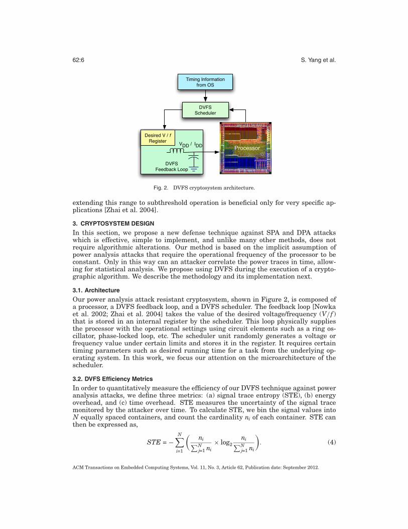
Fig. 2. DVFS cryptosystem architecture.
extending this range to subthreshold operation is beneficial only for very specific ap-plications [Zhai et al. 2004].
3. CRYPTOSYSTEM DESIGN
In this section, we propose a new defense technique against SPA and DPA attackswhich is effective, simple to implement, and unlike many other methods, does notrequire algorithmic alterations. Our method is based on the implicit assumption ofpower analysis attacks that require the operational frequency of the processor to beconstant. Only in this way can an attacker correlate the power traces in time, allow-ing for statistical analysis. We propose using DVFS during the execution of a crypto-graphic algorithm. We describe the methodology and its implementation next.
3.1. Architecture
Our power analysis attack resistant cryptosystem, shown in Figure 2, is composed ofa processor, a DVFS feedback loop, and a DVFS scheduler. The feedback loop [Nowkaet al. 2002; Zhai et al. 2004] takes the value of the desired voltage/frequency (V/ f )that is stored in an internal register by the scheduler. This loop physically suppliesthe processor with the operational settings using circuit elements such as a ring os-cillator, phase-locked loop, etc. The scheduler unit randomly generates a voltage orfrequency value under certain limits and stores it in the register. It requires certaintiming parameters such as desired running time for a task from the underlying op-erating system. In this work, we focus our attention on the microarchitecture of thescheduler.
3.2. DVFS Efficiency Metrics
In order to quantitatively measure the efficiency of our DVFS technique against poweranalysis attacks, we define three metrics: (a) signal trace entropy (STE), (b) energyoverhead, and (c) time overhead. STE measures the uncertainty of the signal tracemonitored by the attacker over time. To calculate STE, we bin the signal values intoN equally spaced containers, and count the cardinality ni of each container. STE canthen be expressed as,
STE = −N∑
i=1
(ni∑Nj=1 ni
× log2ni∑Nj=1 ni
). (4)
ACM Transactions on Embedded Computing Systems, Vol. 11, No. 3, Article 62, Publication date: September 2012.

Power Analysis Attack Resistance Engineering by Dynamic Voltage and Frequency Scaling 62:7
In this work, we use power trace entropy (PTE) and time trace entropy (TTE) torepresent the uncertainty of the power and clock period traces, respectively. Thatmeans we bin the power trace signal and clock period trace signal values into Nequally spaced container and count the cardinality of each container. They can becalculated as,
PTE = −N∑
i=1
(pi∑Nj=1 pi
× log2pi∑Nj=1 pi
). (5)
TTE = −N∑
i=1
(ti∑Nj=1 ti
× log2ti∑Nj=1 ti
). (6)
The two traces measure the power consumption and period of each clock cycle, re-spectively, during algorithm execution. Energy and time overhead measure the over-heads caused by using DVFS. We define VDDnormal and Fnormal as the normal supply volt-age and frequency for the processor without DVFS. In general, they are the highestsupply voltage and frequency. When the supply voltage is switched to a lower valueVDDscale , the operating frequency fscale is scaled as follows:
fscale =(VDDscale − Vth)1.3
VDDscale
× Fnormal, (7)
where Vth is the threshold voltage. Finally, energy and time overhead using DVFS canbe expressed as follows:
Energy Overhead =TNCC∑
i=1
12
Ci(V2
DDscale− V2
DDnormal
)(8)
Time Overhead =TNCC∑
i=1
(1
fscale− 1
Fnormal
), (9)
where TNCC is the total number of clock cycles, and Ci is the capacitive load duringthe ith clock cycle.
3.3. Experimental Setup
We make the following reasonable assumptions before describing our cryptosystem de-sign and experimental results. In order to test the efficiency of the DVFS scheduler,the underlying hardware of the DVFS feedback loop is assumed to be already realized,and implements DVFS in the range of 0.9–1.8V/250–450MHz. Furthermore, we ab-stract its function as a software program to communicate with the processor and thescheduler. The power overhead for the processor switching from high-voltage/high-frequency mode to low-voltage/low-frequency mode, and vice versa, is negligible. Thishas been shown to be reasonable in Nowka et al. [2002] and Zhai et al. [2004]. Thepower consumption of the scheduler and the feedback unit is not measured duringthe power traces, and is much less than that consumed by the processor. For the pro-cessor, the supply voltage and operating frequency can be changed instantly duringany clock cycle. This is an ideal condition. When an application runs for thousandsof clock cycles, this assumption tends to be true from a statistical viewpoint as thevoltage/frequency switching may take just a few clock cycles.
In this work, we implement the DES encryption and decryption algorithms in soft-ware as benchmarks, and capture their energy consumption at each clock cycle when
ACM Transactions on Embedded Computing Systems, Vol. 11, No. 3, Article 62, Publication date: September 2012.

62:8 S. Yang et al.
Algorithm 1 Generate random voltage/frequency (naive design).
Require: VDDnormal, Fnormal, signal done, rw enable1: while !signal done do2: Generate random VDDscale , fscale using VDDnormal , Fnormal
3: if rw enable then4: Assign VDDscale , fscale to DVFS feedback loop unit register5: end if6: end while
running on the processor by using a customized version of the publicly availableSimplePower [Narayanan et al. 2000]. The processor is based on the architectureof a five-stage pipelined datapath which contains the instruction fetch, decode, exe-cute, memory access, and writeback stages. The simulator uses validated transition-sensitive and cycle-accurate energy models for both the datapath and memory sys-tem. The flexibility of working with the simulator provides us with the ability tomonitor the energy consumed in each cycle as well as the details of the executedinstructions.
3.4. DVFS Scheduler Design
In a power analysis attack, an attacker uncovers the secret key bits by observing somesignificant characteristics in the original and differential power traces after runningthe algorithm many times. If the measured power signal is random, and cannot berepeated by running the algorithm repeatedly with the same plain-text and key, theunderlying secret key cannot be deciphered. Given this, an efficient method to guardagainst such attacks is to realize a random number generating algorithm in the piv-otal design of the cryptosystem (i.e., the DVFS scheduler). We can randomly generatea voltage/frequency value, and store it in the designated register. When these ran-domly generated operational voltages are applied to the processor, the output signalwill achieve the desired property. In the following, we describe the step-by-step imple-mentation of the DVFS scheduler.
3.4.1. First Attempt: Naive Design. For each clock cycle, an initial and naive design ofthe scheduler generates a random voltage value (frequency is determined by Equation(7)). It then informs the feedback loop to physically implement this voltage, and feed itto the processor. Here, we neglect the time consumed to generate the random numberand the time consumed to implement the voltage. This implies that the schedulercan generate as many random numbers as desired during a clock cycle. Similarly, thefeedback look can implement all these voltages. With this assumption, we can analyzethe effectiveness of DVFS against power analysis attacks under the extreme condition.
The naive implementation is shown in Algorithm 1. The procedure takes VDDnormal ,Fnormal, signal done, and rw enable as inputs; the first two signals come from the op-erating system and provide initial values, the third signal is from the processor toindicate whether encryption/decryption has finished or not, and the fourth signal issent out from the feedback loop to reveal the status of the internal register. We testedthis algorithm with the DES encryption algorithm in the processor, and measured thepower signal using SimplePower. In order to make the statistical results confident, theDES algorithm was run for 1,000 times on the native implementation.
Figure 3(a) shows the power trace of the DES encryption algorithm when runningon the processor without DVFS. It clearly reveals the 16 rounds of DES operation.Figure 3(b) illustrates the power profile using DVFS with the naive implementation(Algorithm 1). Although there is marginal improvement on information leakage, it still
ACM Transactions on Embedded Computing Systems, Vol. 11, No. 3, Article 62, Publication date: September 2012.

Power Analysis Attack Resistance Engineering by Dynamic Voltage and Frequency Scaling 62:9
Fig. 3. Per clock cycle power trace for DES encryption using Algorithm 1.
Table I. Performance Comparison
Energy Overhead Time Overhead PTE TTE LTWEw/o DVFS 0 0 4.96 0
naive DVFS −35.17% 26.55% 5.05 6.65Improved DVFS
Long waiting time −34.18% 25.15% 5.20 3.17Short waiting time −35.23% 26.21% 5.33 5.97
Advanced DVFSEncryption −27.32% 16.15% 5.42 6.02 NoDecryption −26.89% 16.01% 5.44 6.05 No
makes the 16 rounds obvious. This phenomenon can be explained by realizing thateach round requires about 105 clock cycles with the total operation requiring about211,000 clock cycles. For each round, both the high and low power peak values lastfor about 2.5 × 10⁴ clock cycles. Although the voltage/frequency is randomly changedevery clock cycle which makes the power value at each cycle be a random number, thepower peak values still appear when the power trace is plotted over a big sample timeof 2.5 × 10⁴ clock cycles. This observation makes the naive implementation unable tomask the power consumption, and prevent information leakage. Furthermore, Table Ilists the performance metrics for all our designs. For the naive implementation, weobserve that with an increase in the entropies of the power and time traces, there is abig reduction in the total energy consumption, and a big increase in the total executiontime compared with that without DVFS.
3.4.2. Second Attempt: Improved Design. The improved design is shown in Algorithm 2.Unlike the naive design where the voltage/frequency is changed every clock cycle, thescheduler in the improved design waits for a random time period before generating thenext random voltage/frequency. Consequently, there are two time periods introducedin this implementation: (a) the time consumed by the random number generation al-gorithm, and (b) the waiting time. Note that we neglect the time consumed for volt-age/frequency physical implementation in the feedback loop, and we treat it as a fixedtime. The first time period is constant while the second is random. As a final effect,the voltage/frequency is changed randomly in terms of value and generation time. Inorder to test the efficiency of this implementation, power consumption and clock periodare calculated every clock cycle.
ACM Transactions on Embedded Computing Systems, Vol. 11, No. 3, Article 62, Publication date: September 2012.

62:10 S. Yang et al.
Algorithm 2 Generate random voltage/frequency (improved design).
Require: VDDnormal , Fnormal, signal done, rw enable1: Generate random VDDscale , fscale using VDDnormal , Fnormal
2: Assign VDDscale , fscale to DVFS feedback loop unit register3: while !signal done do4: Generate random NCC5: for i = 1 to NCC do6: NOP7: end for8: Generate random VDDscale , fscale
9: if rw enable then10: Assign VDDscale , fscale to DVFS feedback loop unit register11: end if12: end while
Fig. 4. Comparison between (a)–(b) long and (c)–(d) short random waiting times in power consumption andclock period traces using Algorithm 2.
Figure 4 illustrates the power consumption and clock period traces for the improvedimplementation under two typical cases. The first case has long random waiting timesbetween two voltage/frequency generations. For the entire program execution time,the scheduler only generates ten random values. The second case has short waitingtimes, and the scheduler generates 211 random values. It can be seen that the firstcase still prevents information masking as the 16 rounds of DES operation are obvious.
ACM Transactions on Embedded Computing Systems, Vol. 11, No. 3, Article 62, Publication date: September 2012.
Power Analysis Attack Resistance Engineering by Dynamic Voltage and Frequency Scaling 62:11
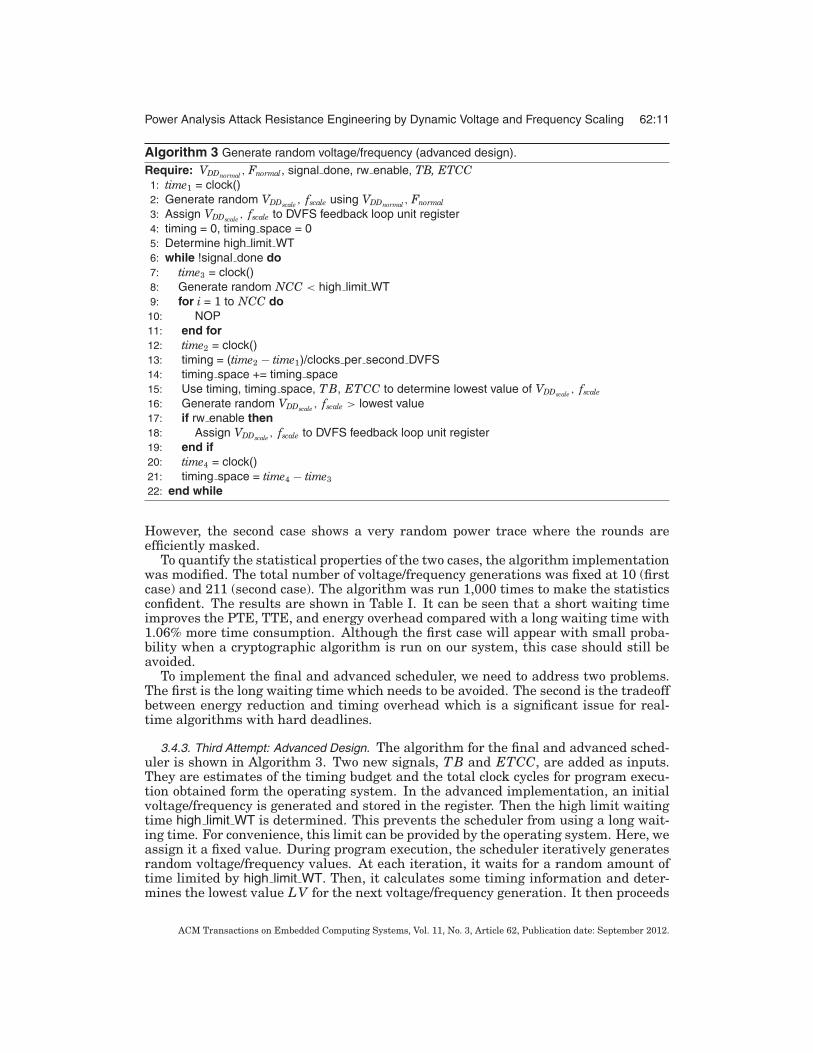
Algorithm 3 Generate random voltage/frequency (advanced design).
Require: VDDnormal , Fnormal, signal done, rw enable, TB, ETCC1: time1 = clock()2: Generate random VDDscale , fscale using VDDnormal , Fnormal
3: Assign VDDscale , fscale to DVFS feedback loop unit register4: timing = 0, timing space = 05: Determine high limit WT6: while !signal done do7: time3 = clock()8: Generate random NCC < high limit WT9: for i = 1 to NCC do10: NOP11: end for12: time2 = clock()13: timing = (time2 − time1)/clocks per second DVFS14: timing space += timing space15: Use timing, timing space, TB, ETCC to determine lowest value of VDDscale , fscale
16: Generate random VDDscale , fscale > lowest value17: if rw enable then18: Assign VDDscale , fscale to DVFS feedback loop unit register19: end if20: time4 = clock()21: timing space = time4 − time3
22: end while
However, the second case shows a very random power trace where the rounds areefficiently masked.
To quantify the statistical properties of the two cases, the algorithm implementationwas modified. The total number of voltage/frequency generations was fixed at 10 (firstcase) and 211 (second case). The algorithm was run 1,000 times to make the statisticsconfident. The results are shown in Table I. It can be seen that a short waiting timeimproves the PTE, TTE, and energy overhead compared with a long waiting time with1.06% more time consumption. Although the first case will appear with small proba-bility when a cryptographic algorithm is run on our system, this case should still beavoided.
To implement the final and advanced scheduler, we need to address two problems.The first is the long waiting time which needs to be avoided. The second is the tradeoffbetween energy reduction and timing overhead which is a significant issue for real-time algorithms with hard deadlines.
3.4.3. Third Attempt: Advanced Design. The algorithm for the final and advanced sched-uler is shown in Algorithm 3. Two new signals, TB and ETCC, are added as inputs.They are estimates of the timing budget and the total clock cycles for program execu-tion obtained form the operating system. In the advanced implementation, an initialvoltage/frequency is generated and stored in the register. Then the high limit waitingtime high limit WT is determined. This prevents the scheduler from using a long wait-ing time. For convenience, this limit can be provided by the operating system. Here, weassign it a fixed value. During program execution, the scheduler iteratively generatesrandom voltage/frequency values. At each iteration, it waits for a random amount oftime limited by high limit WT. Then, it calculates some timing information and deter-mines the lowest value LV for the next voltage/frequency generation. It then proceeds
ACM Transactions on Embedded Computing Systems, Vol. 11, No. 3, Article 62, Publication date: September 2012.
62:12 S. Yang et al.
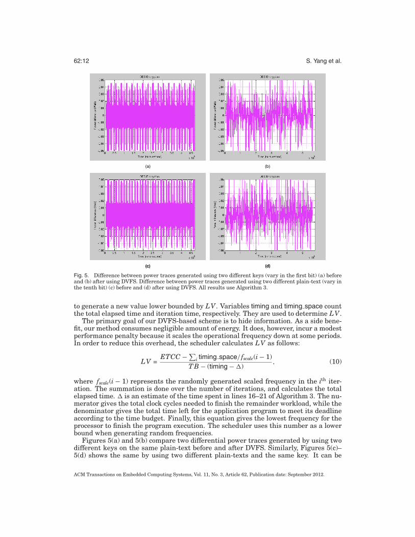
Fig. 5. Difference between power traces generated using two different keys (vary in the first bit) (a) beforeand (b) after using DVFS. Difference between power traces generated using two different plain-text (vary inthe tenth bit) (c) before and (d) after using DVFS. All results use Algorithm 3.
to generate a new value lower bounded by LV. Variables timing and timing space countthe total elapsed time and iteration time, respectively. They are used to determine LV.
The primary goal of our DVFS-based scheme is to hide information. As a side bene-fit, our method consumes negligible amount of energy. It does, however, incur a modestperformance penalty because it scales the operational frequency down at some periods.In order to reduce this overhead, the scheduler calculates LV as follows:
LV =ETCC − ∑
i timing space/ fscale(i − 1)TB − (timing − �)
, (10)
where fscale(i − 1) represents the randomly generated scaled frequency in the ith iter-ation. The summation is done over the number of iterations, and calculates the totalelapsed time. � is an estimate of the time spent in lines 16–21 of Algorithm 3. The nu-merator gives the total clock cycles needed to finish the remainder workload, while thedenominator gives the total time left for the application program to meet its deadlineaccording to the time budget. Finally, this equation gives the lowest frequency for theprocessor to finish the program execution. The scheduler uses this number as a lowerbound when generating random frequencies.
Figures 5(a) and 5(b) compare two differential power traces generated by using twodifferent keys on the same plain-text before and after DVFS. Similarly, Figures 5(c)–5(d) shows the same by using two different plain-texts and the same key. It can be
ACM Transactions on Embedded Computing Systems, Vol. 11, No. 3, Article 62, Publication date: September 2012.
Power Analysis Attack Resistance Engineering by Dynamic Voltage and Frequency Scaling 62:13
seen that without DVFS, significant information is leaked. However, this is preventedwhen using the advanced scheduler.
Two factors contribute to this desirable property of our cryptosystem. When theprogram runs for the first time, operation A is executed at time t. It is executed againat time t + �t, where �t represents a negative or positive time shift. With high prob-ability, this is not equal to zero. Consequently, at a fixed time point for many powertraces which are achieved by using different plain-texts or keys, different operationsare carried out in the processor. This makes time correlation, a very important step inpower analysis attacks, impossible. Second, even if the same operation is executed attime t, the supply voltages for different runs may be different with higher probability.This makes the power values at time t for different traces unequal, resulting in a ran-dom number for DPA bias signals. These two aspects efficiently make it much harderto employ SPA and DPA attacks on our cryptosystem.
Table I shows the performance of the advanced design. It also includes the long timewaiting effect (LTWE). We can see that the PTE and TTE are greatly increased, andmuch higher than the improved implementation. As a result, LTWE does not exist inthis case. Furthermore, the time overhead is significantly reduced as well. By com-paring all three implementations, it can be seen that the advanced version overcomesthe shortcomings of the naive and improved designs. By adjusting the lowest valuefor VDDscale , Fscale in the algorithm to be a higher value, we can further reduce the timeoverhead. Experiments show that this range for DES encryption and decryption isabout 5–17%.
3.5. Counterattack Analysis
In this section, we analyze the difficulty of breaking the DVFS cryptosystem. Assumethat it is implemented as a system-on-chip. For the processor, its power trace is a func-tion of supply voltage and frequency. A typical case is that it implements seven dif-ferent voltage/frequency values (e.g., Intel XScale). Once the supply voltage is known,the corresponding frequency can be determined by Equation (7).
In order to correlate traces for DPA, the attacker needs to align different powertraces with the same supply voltage and frequency. This requires mathematical trans-formation of the measured power trace with DVFS to filter out the effects of DVFS.This kind of transformation, either in time or frequency domain, is very difficult. Ifthe attacker knows when the voltage/frequency is changed, and which values it ischanged to, aligning different power trances with the same frequency is easy by timeshifting. However, mathematically scaling a DVFS power trace by using the samesupply voltage at each clock cycle, although easy to implement, is meaningless. Fur-thermore, it is quite different from the measured power trance under the same supplyvoltage without DVFS. The reason is simple. Changing the supply voltage alters alot of physical information like leakage current, chip temperature, capacitance charg-ing/discharging speed, etc. Consequently, it is impossible to use the supply voltage tomodel the change of power consumption caused by changing the supply voltage. Thisimplies that transforming power traces to filter out DVFS effects is difficult by justutilizing the knowledge of supply voltage.
Now suppose the attacker already knows the transformation by taking advantageof complicated statistics of the DVFS processor. Furthermore, assume that the at-tacker also knows the seven different voltage/frequency values, and has full knowl-edge of when these parameters are changed. Suppose there are 200 voltage/frequencychanges. At each point, there are seven possibilities. In order to perform DPA, the at-tacker is required to know which voltage/frequency is applied during some time period.Using a brute-force method, the attack would have to try 7200 combinations. Suppose
ACM Transactions on Embedded Computing Systems, Vol. 11, No. 3, Article 62, Publication date: September 2012.

62:14 S. Yang et al.
each trial takes 1 ns (this time period is too short and is a limit for 1GHz processor).It will take 7200
109×3600×24×365 = 3.32 × 10152 succeed. This is impractical. Future work onhardness analysis will be conducted to discuss whether a combination of attacks (e.g.,electromagnetic-based + DPA attack) could make it possible to derive the correlationof differential power traces with dynamic voltage scaling values and timing.
4. CONCLUSIONS
In this work, we presented the design of a novel power analysis attack resistant cryp-tosystem which uses DVFS to create random power traces. This prevents an attackerfrom being able to perform time correlation between different power traces. Experi-ments were carried out on three design variants: naive, improved, and advanced. Theytested the efficacy of using DVFS to improve the resistance of a cryptosystem to DPAattacks. The advanced scheduler overcame the shortcomings of the other designs, andexhibited good efficiency in blocking DPA attacks. DES encryption and decryption al-gorithms were used as benchmarks. The results showed that both power and timetrace entropies were high enough to prevent information leakage. While the energyconsumption was reduced by 27% on average, the execution time was delayed by 16%.Finally, we performed hardness analysis on the DVFS method, and showed that itwould be impractical to counterattack by using a brute-force method.
ACKNOWLEDGMENTS
The authors would like to thank the reviewers for their invaluable and very insightful comments. They havehelped us to improve this work significantly.
REFERENCESBENINI, L., GALATI, A., MACII, A., MACII, E., AND PONCINO, M. 2003a. Energy-efficient data scrambling
on memory-processor interfaces. In Proceedings of the International Symposium on Low Power Electron-ics and Design. 26–29.
BENINI, L., MACII, A., MACII, E., OMERBEGOVIC, E., PONCINO, M., AND PRO, F. 2003b. Energy-awaredesign techniques for differential power analysis protection. In Proceedings of the Design AutomationConference. 36–41.
BONEH, D., DEMILLO, R., AND LIPTON, R. 2001. On the importance of eliminating errors in cryptographiccomputations. J. Cryptol. 14, 2, 101–119.
BURD, T., PERING, T., STRATAKOS, A., AND BRODERSEN, R. 2000. A dynamic voltage scaled microprocessorsystem. IEEE Trans. Syst. Sci. Cybern. 35, 11, 1571–1580.
BURD, T. D. AND BRODERSEN, R. 2000. Design issues for dynamic voltage scaling. 9–14.
BURD, T. D., PERING, T. A., STRATAKOS, A. J., AND BRODERSEN, R. W. 2002. A dynamic voltage scaledmicroprocessor system. IEEE J. Solid-State Circ. 35, 11, 1571–1580.
CHEVALLIER-MAMES, B., CIET, M., AND JOYE, M. 2004. Low-cost solutions for preventing simple side-channel analysis: Side-channel atomicity. IEEE Trans. Comput. 53, 6, 760–768.
CHOI, K., SOMA, R., AND PEDRAM, M. 2004. Off-chip latency-driven dynamic voltage and frequency scalingfor an MPEG decoding. In Proceedings of the 41st Annual Design Automation Conference. 544–549.
CORON, J. 1999. Resistance against differential power analysis for elliptic curve cryptosystems. In Proceed-ings of the International Workshop on Cryptographic Hardware & Embedded Systems. 292–302.
GHIASI, S., CASMIRA, J., AND GRUNWALD, D. 2000. Using IPC variation in workload with externally speci-fied rates to reduce power consumption. In Proceedings of the Workshop on Complexity-Effective Design.
GIANCANE, L., MARIETTI, P., OLIVIERI, M., SCOTTI, G., AND TRIFILETTI, A. 2008. A new dynamic dif-ferential logic style as a countermeasure to power analysis attacks. In Proceedings of the InternationalConference on Electronics, Circuits and Systems. 364–367.
ACM Transactions on Embedded Computing Systems, Vol. 11, No. 3, Article 62, Publication date: September 2012.

Power Analysis Attack Resistance Engineering by Dynamic Voltage and Frequency Scaling 62:15
GOUBIN, L. AND PATARIN, J. 1999. DES and differential power analysis - the duplication method.In Proceedings of the International Workshop on Cryptographic Hardware & Embedded Systems.158–172.
GUILEY, S., SAUVAGE, L., HOOGVORST, P., PACALET, R., BERTONIAN, G. M., AND CHAUDHURI, S. 2008.Security evaluation of WDDL and SecLib countermeasures against power attacks. IEEE Trans. Comput.57, 11, 1482–1497.
KHATIBZADEH, A. AND GEBOTYS, C. 2007. Enhanced current-balanced logic (ECBL): An area efficientsolution to secure smart cards against differential power attack. In Proceedings of the InternationalConference on Information Technology. 898–899.
KOCHER, P. 1996. Timing attacks on implementations of Diffe-Hellman, RSA, DSS and other systems. InProceedings of the Conference on Advances in Cryptology. 104–113.
KOCHER, P., JAFFE, J., AND JUN, B. 1999. Differential power analysis. In Proceedings of the Conference onAdvances in Cryptology. 388–397.
KOCHER, P., LEE, R., MCGRAW, G., RAGHUNATHAN, A., AND RAVI, S. 2004. Security as a new dimension inembedded system design. In Proceedings of the 41st Design Automation Conference (DAC’04). 753–760.
KOMMERLING, O. AND KUHN, M. G. 1999. Design principles for tamper-resistant smartcard processors. InProceedings of the USENIX Workshop on Smartcard Technology. 1–12.
KOOPMAN, P. 2004. Embedded system security. IEEE Computer 37, 2 (July), 95–97.LORCH, J. R. AND SMITH, A. J. 2004. PACE: A new approach to dynamic voltage scaling. IEEE Trans.
Comput. 53, 7, 856–869.LUO, J., JHA, N. K., AND PEH, L. 2007. Simultaneous dynamic voltage scaling of processors and communi-
cation links in real-time distributed embedded systems. IEEE Trans. VLSI Syst. 15, 4, 427–437.MOORE, S., ANDERSON, R., CUNNINGHAM, P., MULLINS, R., AND TAYLOR, G. 2002. Improving smart
card security using self-timed circuits. In Proceedings of the International Symposium on AsynchronousCircuits & Systems. 211–218.
NARAYANAN, V., KANDEMIR, M., IRWIN, M. J., KIM, H. S., AND YE, W. 2000. Energy-driven integratedhardware-software optimizations using SimplePower. In Proceedings of the Annual International Sym-posium on Computer Architecture. 95–106.
NOWKA, K. J., CARPENTER, G. D., MACDONALD, E. W., NGO, H. C., BROCK, B. C., ISHII, K. I., NGUYEN,T. Y., AND BURNS, J. L. 2002. A 32-bit PowerPC system-on-a-chip with support for dynamic voltagescaling and dynamic frequency scaling. IEEE J. Solid-State Circ. 37, 11, 1441–1447.
QUISQUATER, J. J. AND SAMYDE, D. 2001. Electromagnetic analysis (EMA): Measures and counter-measures for smart cards. In Proceedings of the Conference on Research in Smart Cards. 200–210.
QUISQUATER, J. J. AND SAMYDE, D. 2002. Side-channel cryptanalysis. In Proceedings of Securite de laCommunication sur Internet (SECI’02). 179–184.
RATANPAL, G. B., WILLIAMS, R. D., AND BLALOCK, T. N. 2004. An on-chip signal suppression countermea-sure to power analysis attacks. IEEE Trans. Dependable Secure Comput. 1, 3, 179–189.
RAVI, S., RAGHUNATHAN, A., AND CHAKRADHAR, S. 2003. Embedding security in wireless embedded sys-tems. In Proceedings of the 16th International Conference on VLSI Design. 269–270.
REAL, D., CLEDIERE, J., CANOVAS, C., DRISSI, M., AND VALETTE, F. 2008. Defeating classical hardwarecountermeasures: A new processing for side channel analysis. In Proceedings of the Conference on De-sign, Automation and Test in Europe. 1274–1279.
REGAZZONI, F., EISENBARTH, T., GROBSCHADL, J., BREVEGLIERI, L., IENNE, P., KOREN, I., AND PAAR,C. 2007. Power attacks resistance of cryptographic S-boxes with added error detection circuits. In Pro-ceedings of the International Symposium on Defect & Fault Tolerance in VLSI Systems. 508–516.
ROHATGI, P. 2010. Protecting FPGAs from power analysis. Tech. rep., Cryptography Research Inc.SAPUTRA, H., NARAYANAN, V., KANDEMIR, M., IRWIN, M. J., BROOKS, R., AND ZHANG, S. K. W. 2003.
Masking the energy behavior of DES encryption. IEE Proc. Comput. Digital Techn., 84–89.SCHNEIER, B. 1996. Applied Cryptography, Protocols, Algorithms, and Source Code in C. John Wiley, New
York, NY.SEN, S., HOSSAIN, S. I., ISLAM, K., CHOWDHURI, D. R., AND CHAUDHURI, P. P. 2003. Cryptosystem
designed for embedded system security. In Proceedings of the 16th International Conference on VLSIDesign. 271–276.
TIRI, K. AND VERBAUWHEDE, I. 2003. Securing encryption algorithms against DPA at the logic level: nextgeneration smart card technology. In Proceedings of the International Workshop on Cryptographic Hard-ware and Embedded Systems. 125–136.
ACM Transactions on Embedded Computing Systems, Vol. 11, No. 3, Article 62, Publication date: September 2012.

62:16 S. Yang et al.
WAGNER, D. AND WADDLE, J. 2004. Towards efficient second-order power analysis. In Proceedings of theInternational Workshop on Cryptographic Hardware & Embedded Systems. 1–15.
XIAN, C., LU, Y. H., AND LI, Z. 2008. Dynamic voltage scaling for multitasking real-time systems withuncertain execution time. IEEE Trans. Comput.-Aided Design Integr. Circ. Syst. 27, 8, 1467–1478.
ZHAI, B., BLAAUW, D., SYLVESTER, D., AND FLAUTNER, K. 2004. Theoretical and practical limits of dy-namic voltage scaling. In Proceedings of the 41st Annual Design Automation Conference. 868–873.
Received June 2009; revised May 2010; accepted July 2010
ACM Transactions on Embedded Computing Systems, Vol. 11, No. 3, Article 62, Publication date: September 2012.