Embed Size (px)
Citation preview

1
Power Electoric (Tutotrial)
(Power / Network)
Technical Electric Department
Technical Institute of Mosul
2
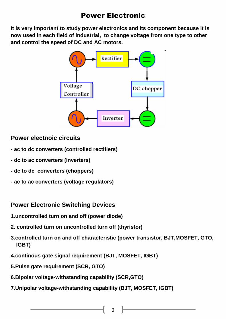
Power Electronic
It is very important to study power electronics and its component because it is
now used in each field of industrial, to change voltage from one type to other
and control the speed of DC and AC motors.
Power electnoic circuits
- ac to dc converters (controlled rectifiers)
- dc to ac converters (inverters)
- dc to dc converters (choppers)
- ac to ac converters (voltage regulators)
Power Electronic Switching Devices
1.uncontrolled turn on and off (power diode)
2. controlled turn on uncontrolled turn off (thyristor)
3.controlled turn on and off characteristic (power transistor, BJT,MOSFET, GTO,
IGBT)
4.continous gate signal requirement (BJT, MOSFET, IGBT)
5.Pulse gate requirement (SCR, GTO)
6.Bipolar voltage-withstanding capability (SCR,GTO)
7.Unipolar voltage-withstanding capability (BJT, MOSFET, IGBT)

3
8.Bidirectional current capability (TRIAC)
9.Undirectional current capability (SCR, GTO, BJT, MOSFET, IGBT)
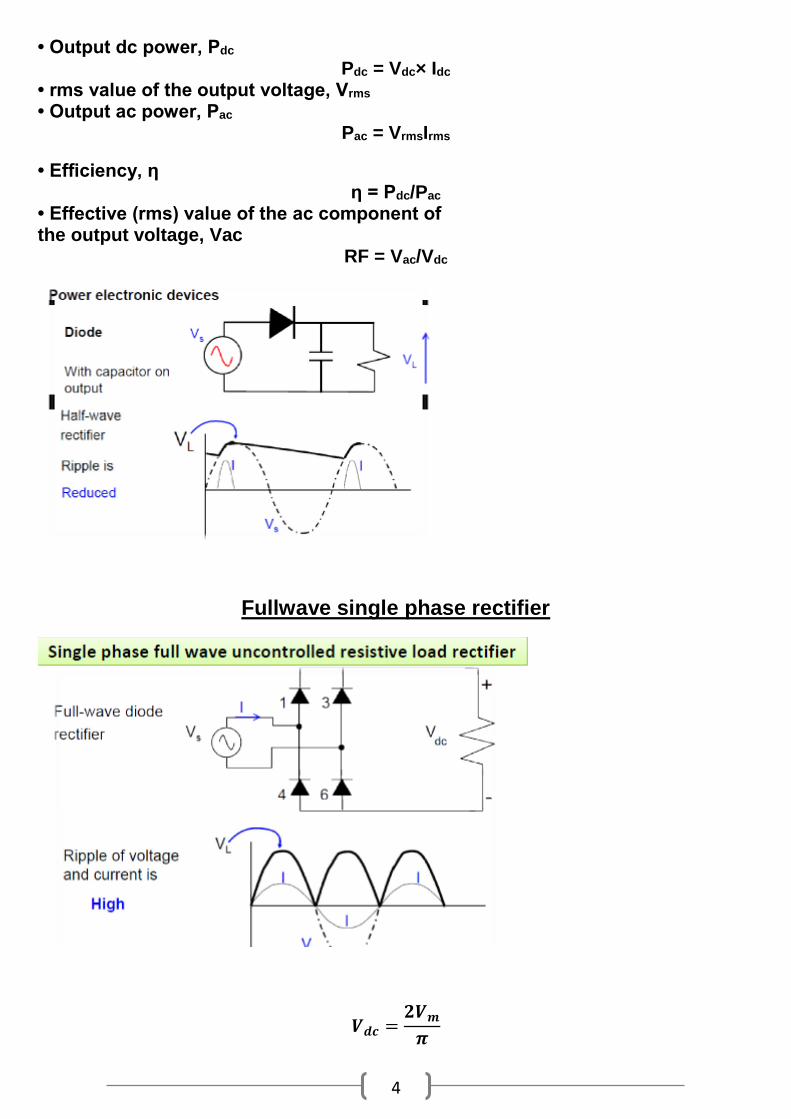
Uncontrolled rectifiers
Circuits which use power diods
Single phase rectifiers
Half wave single phase rectifiers
The main disadvantages of half wave rectifier are:
1. High ripple factor. 2. Low rectification efficiency. 3. Low transformer utilization factor, and 4. DC saturation of transformer secondary winding.
𝑽𝒅𝒄 =𝑽𝒎
𝝅
• Average value of the output voltage, Vdc • Average value of the output current, Idc
4
• Output dc power, Pdc Pdc = Vdc× Idc
• rms value of the output voltage, Vrms • Output ac power, Pac
Pac = VrmsIrms
• Efficiency, η η = Pdc/Pac
• Effective (rms) value of the ac component of the output voltage, Vac
RF = Vac/Vdc
Fullwave single phase rectifier
𝑽𝒅𝒄 =𝟐𝑽𝒎
𝝅
5
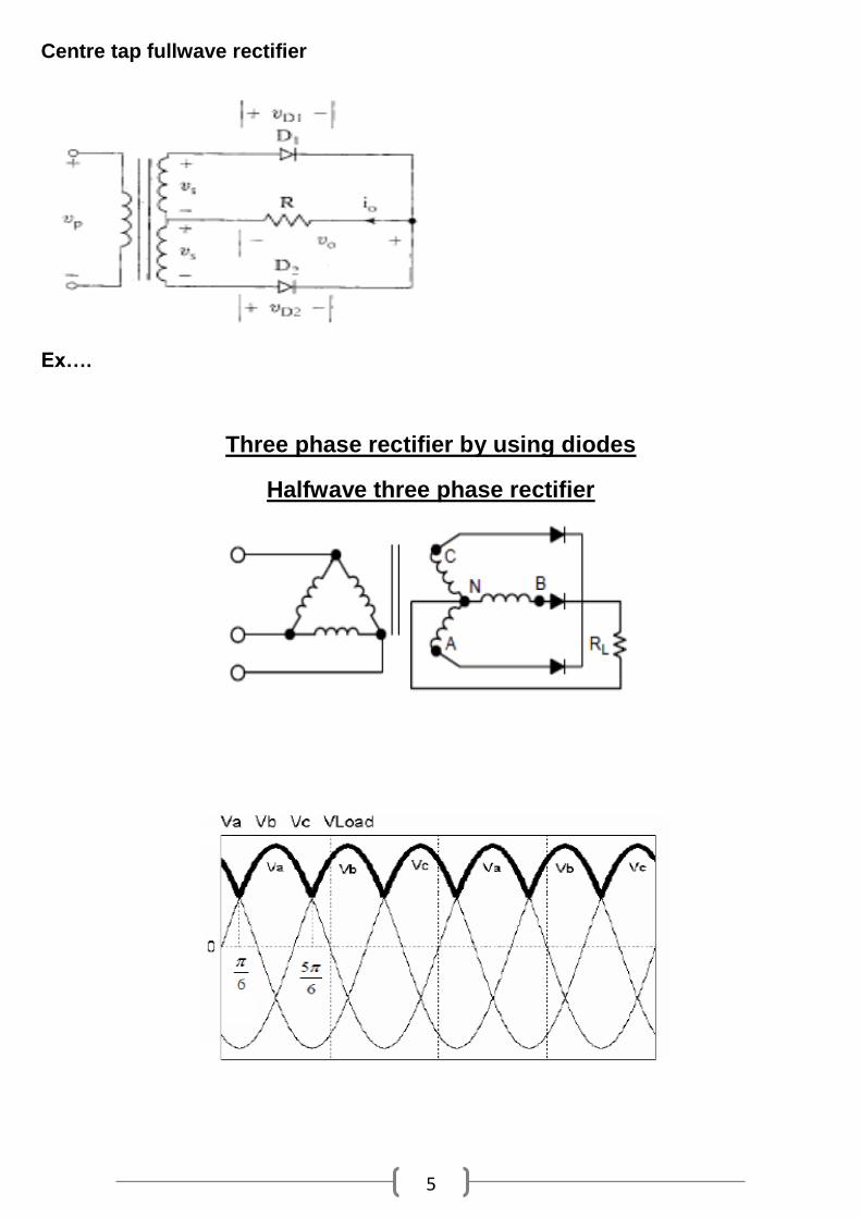
Centre tap fullwave rectifier
Ex….
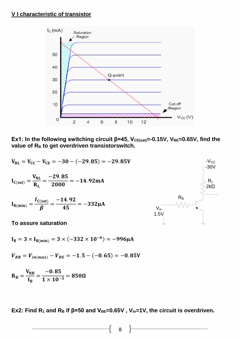
Three phase rectifier by using diodes
Halfwave three phase rectifier

6
𝑽𝒅𝒄 =𝟑√𝟑𝑽𝒎
𝝅
𝑽𝒅𝒄 = 𝟎. 𝟖𝟐𝟕𝑽𝒎
Fullwave three phase rectifier

7
𝑽𝒅𝒄 =𝟑𝑽𝒎
= 𝝅
Ex…..
Transistor as Switche (fully controlled switch)
Look at this one circuit as two separate circuits, the base-emitter(left side) circuit and the collector emitter(right side) circuit. Note that the emitter leg serves as a conductor for both circuits. The amount of current flow in the base-emitter circuit controls the amount of current that flows in the collector circuit. Small changes in base-emitter current yields a largechange in collector-current.
The factor of this change is calledbeta β= IC/IB
8
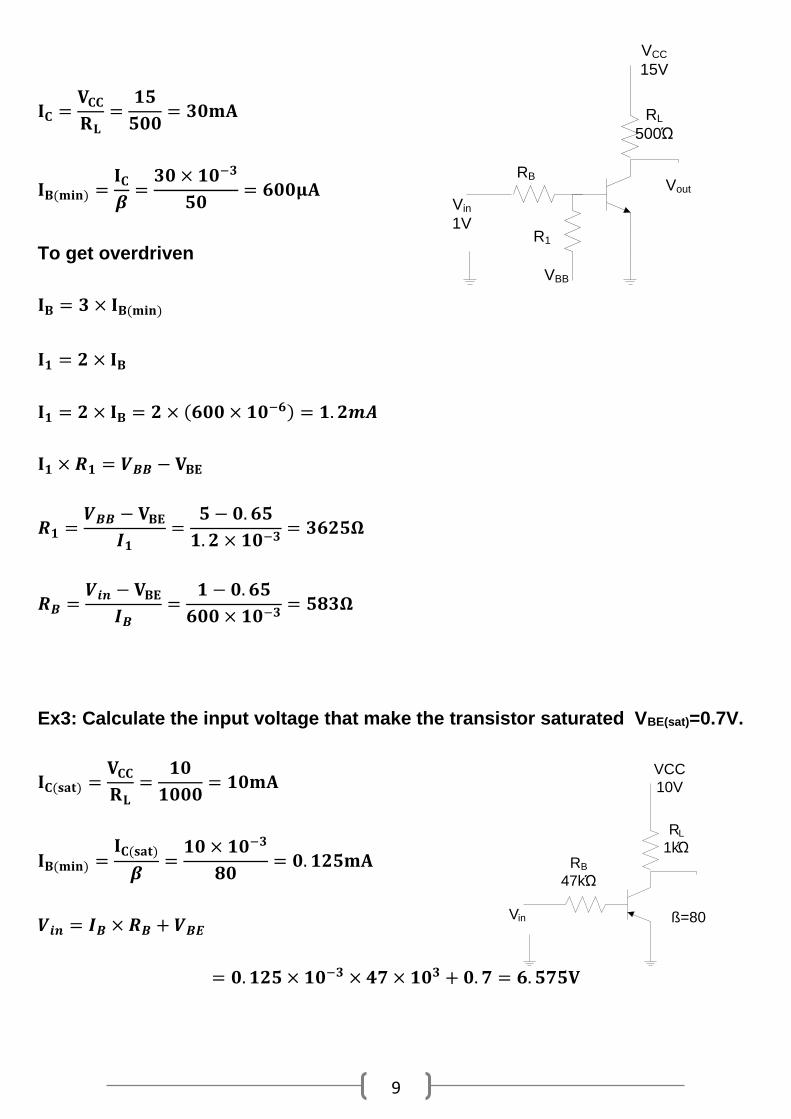
V I characteristic of transistor
Ex1: In the following switching circuit β=45, VCE(sat)=-0.15V, VBE=0.65V, find the value of RB to get overdriven transistorswitch.
𝐕𝐑𝐋 = 𝐕𝐂𝐂 − 𝐕𝐂𝐄 = −𝟑𝟎 − (−𝟐𝟗. 𝟖𝟓) = −𝟐𝟗. 𝟖𝟓𝐕
𝐈𝐂(𝐬𝐚𝐭) =𝐕𝐑𝐋
𝐑𝐋=
−𝟐𝟗. 𝟖𝟓
𝟐𝟎𝟎𝟎= −𝟏𝟒. 𝟗𝟐𝐦𝐀
𝐈𝐁(𝐦𝐢𝐧) =𝑰𝐂(𝐬𝐚𝐭)
𝜷=
−𝟏𝟒. 𝟗𝟐
𝟒𝟓= −𝟑𝟑𝟐𝛍𝐀
To assure saturation
𝐈𝐁 = 𝟑 × 𝐈𝐁(𝐦𝐢𝐧) = 𝟑 × (−𝟑𝟑𝟐 × 𝟏𝟎−𝟔) = −𝟗𝟗𝟔𝛍𝐀
𝑽𝑹𝑩 = 𝑽𝒊𝒏(𝒎𝒂𝒙) − 𝑽𝑩𝑬 = −𝟏. 𝟓 − (−𝟎. 𝟔𝟓) = −𝟎. 𝟖𝟓𝐕
𝐑𝐁 =𝐕𝐑𝐁
𝐈𝐁=
−𝟎. 𝟖𝟓
𝟏 × 𝟏𝟎−𝟑= 𝟖𝟓𝟎𝛀
Ex2: Find R1 and RB if β=50 and VBE=0.65V , Vin=1V, the circuit is overdriven.
RB
RL
2kΏ
-VCC
-30V
Vin
1.5V
9
𝐈𝐂 =𝐕𝐂𝐂
𝐑𝐋=
𝟏𝟓
𝟓𝟎𝟎= 𝟑𝟎𝐦𝐀
𝐈𝐁(𝐦𝐢𝐧) =𝐈𝐂
𝜷=
𝟑𝟎 × 𝟏𝟎−𝟑
𝟓𝟎= 𝟔𝟎𝟎𝛍𝐀
To get overdriven
𝐈𝐁 = 𝟑 × 𝐈𝐁(𝐦𝐢𝐧)
𝐈𝟏 = 𝟐 × 𝐈𝐁
𝐈𝟏 = 𝟐 × 𝐈𝐁 = 𝟐 × (𝟔𝟎𝟎 × 𝟏𝟎−𝟔) = 𝟏. 𝟐𝒎𝑨
𝐈𝟏 × 𝑹𝟏 = 𝑽𝑩𝑩 − 𝐕𝐁𝐄
𝑹𝟏 =𝑽𝑩𝑩 − 𝐕𝐁𝐄
𝑰𝟏=
𝟓 − 𝟎. 𝟔𝟓
𝟏. 𝟐 × 𝟏𝟎−𝟑= 𝟑𝟔𝟐𝟓𝛀
𝑹𝑩 =𝑽𝒊𝒏 − 𝐕𝐁𝐄
𝑰𝑩=
𝟏 − 𝟎. 𝟔𝟓
𝟔𝟎𝟎 × 𝟏𝟎−𝟑= 𝟓𝟖𝟑𝛀
Ex3: Calculate the input voltage that make the transistor saturated VBE(sat)=0.7V.
𝐈𝐂(𝐬𝐚𝐭) =𝐕𝐂𝐂
𝐑𝐋=
𝟏𝟎
𝟏𝟎𝟎𝟎= 𝟏𝟎𝐦𝐀
𝐈𝐁(𝐦𝐢𝐧) =𝐈𝐂(𝐬𝐚𝐭)
𝜷=
𝟏𝟎 × 𝟏𝟎−𝟑
𝟖𝟎= 𝟎. 𝟏𝟐𝟓𝐦𝐀
𝑽𝒊𝒏 = 𝑰𝑩 × 𝑹𝑩 + 𝑽𝑩𝑬
= 𝟎. 𝟏𝟐𝟓 × 𝟏𝟎−𝟑 × 𝟒𝟕 × 𝟏𝟎𝟑 + 𝟎. 𝟕 = 𝟔. 𝟓𝟕𝟓𝐕
Vout
RB
RL
500Ώ
VCC
15V
Vin
1VR1
VBB
RL
1kΏ
Vin
VCC
10V
RB
47kΏ
ß=80
10
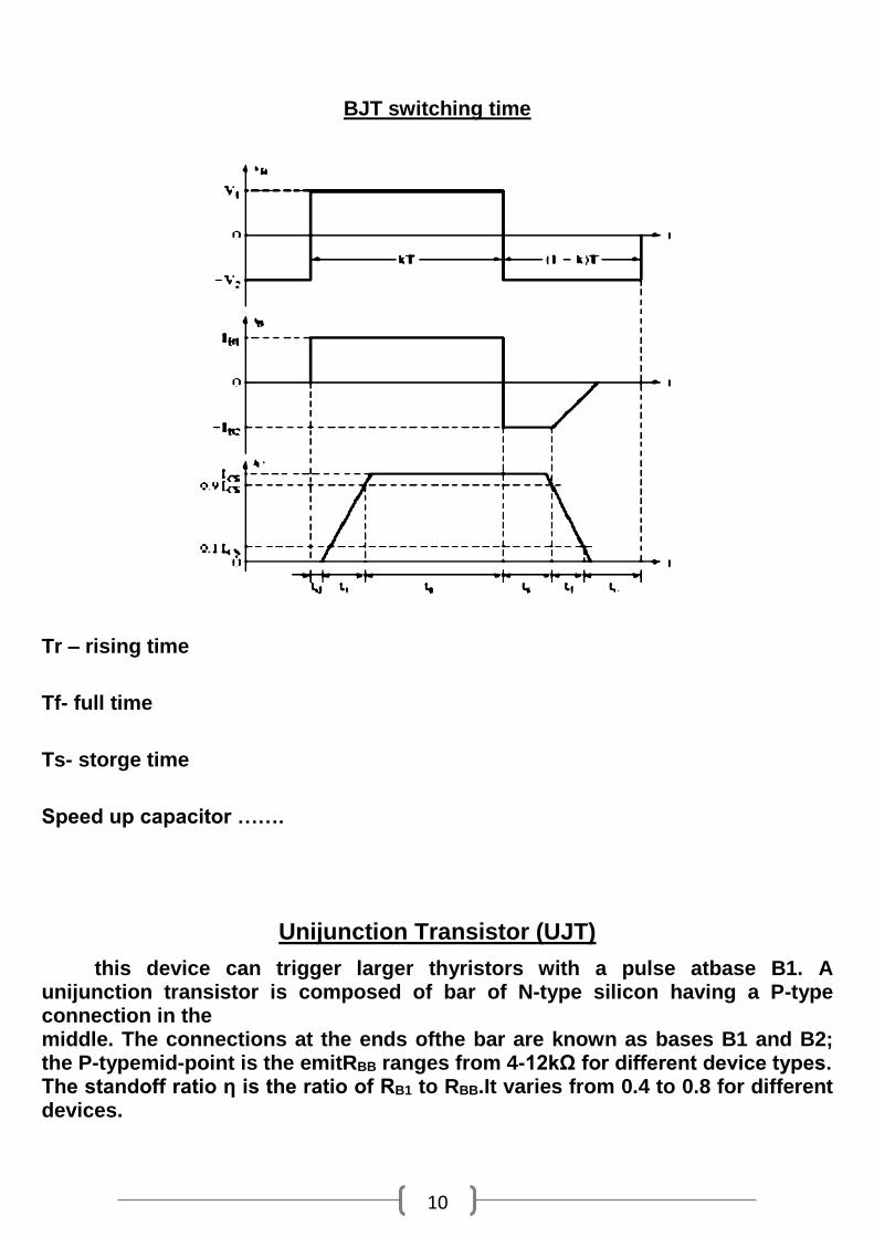
BJT switching time
Tr – rising time
Tf- full time
Ts- storge time
Speed up capacitor …….
Unijunction Transistor (UJT)
this device can trigger larger thyristors with a pulse atbase B1. A unijunction transistor is composed of bar of N-type silicon having a P-type connection in the middle. The connections at the ends ofthe bar are known as bases B1 and B2; the P-typemid-point is the emitRBB ranges from 4-12kΩ for different device types. The standoff ratio η is the ratio of RB1 to RBB.It varies from 0.4 to 0.8 for different devices.

11
UJT Characteristics

12
UJT Relaxation Oscillator
Ex: For relaxation oscillator: calculate maximum and minimum frequencies, and calculate the maximum capacitance voltage.
𝑻 = 𝑹𝑪 × 𝐥𝐧𝟏
𝟏 − 𝜼
𝑹 = 𝑹𝟏 + 𝑹𝟐
𝑹𝒎𝒂𝒙 = 𝟐. 𝟐𝒌Ω + 𝟏𝟎𝟎𝒌𝛀 = 𝟏𝟎𝟐. 𝟐𝒌𝛀
𝑻𝒎𝒂𝒙 = 𝟏𝟎𝟐 × 𝟏𝟎𝟑𝟎. 𝟏 × 𝟏𝟎−𝟔 × 𝐥𝐧𝟏
𝟏 − 𝟎. 𝟔𝟓
= 𝟏𝟎. 𝟕𝟎𝟖𝐦𝐬
𝑭𝒎𝒊𝒏 =𝟏
𝑻= 𝟗𝟑. 𝟑𝟖𝑯𝒛
𝑹𝒎𝒊𝒏 = 𝟐. 𝟐𝒌𝛀 + 𝟎 = 𝟐. 𝟐𝒌𝛀
𝑻𝒎𝒊𝒏 = 𝟐. 𝟐 × 𝟏𝟎𝟑 × 𝟎. 𝟏 × 𝟏𝟎−𝟔 × 𝐥𝐧𝟏
𝟏 − 𝟎. 𝟔𝟓
= 𝟎. 𝟐𝟑𝐦𝐬
Rpot
100kΏ
R1
2.2kΏ
R4
470Ώ
R3
100Ώ
C
0.1µF
B1
η=0.65E
+VCC
12V
13
𝑭𝒎𝒂𝒙 =𝟏
𝑻𝒎𝒊𝒏= 𝟒. 𝟑𝟐𝟗𝑯𝒛
𝑽𝑪 = 𝜼𝑽𝑪𝑪 + 𝑽𝜸
= 𝟎. 𝟔𝟓 × 𝟏𝟐 + 𝟎. 𝟔 = 𝟖. 𝟒𝐕
Operational Amplifier
An integrated circuit (IC) DC amplifier with high open loop gain. It basically has 2 input terminal: Inverting input & Non inverting input (the inverting input inverts the input signal 1800 phase shift) with one output terminal.
Differential Amplifier
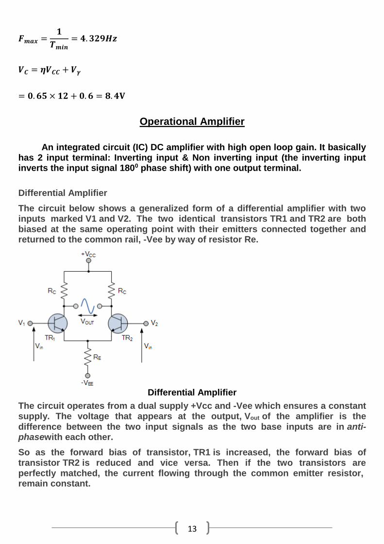
The circuit below shows a generalized form of a differential amplifier with two inputs marked V1 and V2. The two identical transistors TR1 and TR2 are both biased at the same operating point with their emitters connected together and returned to the common rail, -Vee by way of resistor Re.
Differential Amplifier
The circuit operates from a dual supply +Vcc and -Vee which ensures a constant supply. The voltage that appears at the output, Vout of the amplifier is the difference between the two input signals as the two base inputs are in anti-phasewith each other.
So as the forward bias of transistor, TR1 is increased, the forward bias of transistor TR2 is reduced and vice versa. Then if the two transistors are perfectly matched, the current flowing through the common emitter resistor, remain constant.
14
Like the input signal, the output signal is also balanced and since the collector voltages either swing in opposite directions (anti-phase) or in the same direction (in-phase) the output voltage signal, taken from between the two collectors is, assuming a perfectly balanced circuit the zero difference between the two collector voltages.
This is known as the Common Mode of Operation with the common mode gain of the amplifier being the output gain when the input is zero.
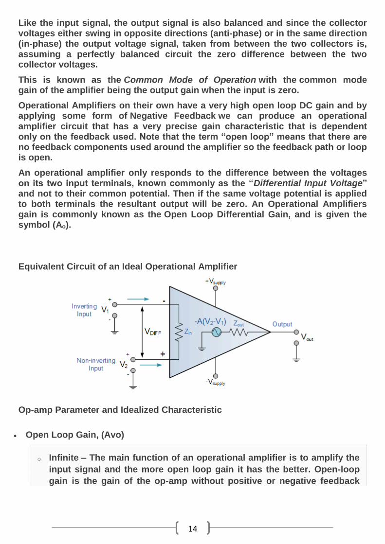
Operational Amplifiers on their own have a very high open loop DC gain and by applying some form of Negative Feedback we can produce an operational amplifier circuit that has a very precise gain characteristic that is dependent only on the feedback used. Note that the term “open loop” means that there are no feedback components used around the amplifier so the feedback path or loop is open.
An operational amplifier only responds to the difference between the voltages on its two input terminals, known commonly as the “Differential Input Voltage” and not to their common potential. Then if the same voltage potential is applied to both terminals the resultant output will be zero. An Operational Amplifiers gain is commonly known as the Open Loop Differential Gain, and is given the symbol (Ao).
Equivalent Circuit of an Ideal Operational Amplifier
Op-amp Parameter and Idealized Characteristic
Open Loop Gain, (Avo)
o Infinite – The main function of an operational amplifier is to amplify the
input signal and the more open loop gain it has the better. Open-loop
gain is the gain of the op-amp without positive or negative feedback
15
and for such an amplifier the gain will be infinite but typical real values
range from about 20,000 to 200,000.
Input impedance, (ZIN)
o Infinite – Input impedance is the ratio of input voltage to input current
and is assumed to be infinite to prevent any current flowing from the
source supply into the amplifiers input circuitry ( IIN = 0 ). Real op-amps
have input leakage currents from a few pico-amps to a few milli-amps.
Output impedance, (ZOUT)
o Zero – The output impedance of the ideal operational amplifier is
assumed to be zero acting as a perfect internal voltage source with no
internal resistance so that it can supply as much current as necessary
to the load. This internal resistance is effectively in series with the load
thereby reducing the output voltage available to the load. Real op-amps
have output impedances in the 100-20kΩ range.
Bandwidth, (BW)
o Infinite – An ideal operational amplifier has an infinite frequency
response and can amplify any frequency signal from DC to the highest
AC frequencies so it is therefore assumed to have an infinite
bandwidth. With real op-amps, the bandwidth is limited by the Gain-
Bandwidth product (GB), which is equal to the frequency where the
amplifiers gain becomes unity.
Offset Voltage, (VIO)
o Zero – The amplifiers output will be zero when the voltage difference
between the inverting and the non-inverting inputs is zero, the same or
when both inputs are grounded. Real op-amps have some amount of
output offset voltage.
From these “idealized” characteristics above, we can see that the input resistance is infinite, so no current flows into either input terminal (the “current rule”) and that the differential input offset voltage is zero (the “voltage rule”). It is important to remember these two properties as they will help us understand the workings of the Operational Amplifier with regards to the analysis and design of op-amp circuits.

16
However, real Operational Amplifiers such as the commonly available uA741, for example do not have infinite gain or bandwidth but have a typical “Open Loop Gain” which is defined as the amplifiers output amplification without any external feedback signals connected to it and for a typical operational amplifier is about 100dB at DC (zero Hz). This output gain decreases linearly with frequency down to “Unity Gain” or 1, at about 1MHz and this is shown in the following open loop gain response curve.
Internal Schematic & Working of IC 741

17
IC 741 Op Amp (Operational Amplifier)
The 741 Op Amp IC is a monolithic integrated circuit, comprising of a general
purpose Operational Amplifier. It was first manufactured by Fairchild
semiconductors in the year 1963. The number 741 indicates that this operational
amplifier IC has 7 functional pins, 4 pins capable of taking input and 1 output
pin.
IC 741 Op Amp can provide high voltage gain and can be operated over a wide
range of voltages, which makes it the best choice for use in integrators,
summing amplifiers and general feedback applications. It also features short
circuit protection and internal frequency compensation circuits built in it.
Inverting Voltage Amplifier using IC741
This arrangement is named as inverting because it amplifies and reverses the
polarity of input signal (Observe the waveforms at the input and output).
Resistor R2 is the feedback resistor. Gain of the amplifier is given by the
formula:
Gain (AV) = -(R2 / R1)
Negative sign indicates that the polarity of the output waveform is reversed. By
adjusting the values of R1 and R2 desired amplification can be achieve
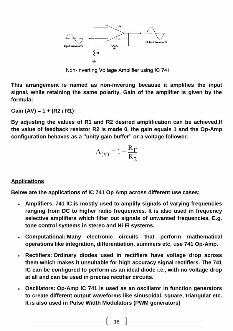
Non-Inverting Voltage Amplifier using IC741
18
This arrangement is named as non-inverting because it amplifies the input
signal, while retaining the same polarity. Gain of the amplifier is given by the
formula:
Gain (AV) = 1 + (R2 / R1)
By adjusting the values of R1 and R2 desired amplification can be achieved.If
the value of feedback resistor R2 is made 0, the gain equals 1 and the Op-Amp
configuration behaves as a “unity gain buffer” or a voltage follower.
Applications
Below are the applications of IC 741 Op Amp across different use cases:
Amplifiers: 741 IC is mostly used to amplify signals of varying frequencies
ranging from DC to higher radio frequencies. It is also used in frequency
selective amplifiers which filter out signals of unwanted frequencies, E.g.
tone control systems in stereo and Hi Fi systems.
Computational: Many electronic circuits that perform mathematical
operations like integration, differentiation, summers etc. use 741 Op-Amp.
Rectifiers: Ordinary diodes used in rectifiers have voltage drop across
them which makes it unsuitable for high accuracy signal rectifiers. The 741
IC can be configured to perform as an ideal diode i.e., with no voltage drop
at all and can be used in precise rectifier circuits.
Oscillators: Op-Amp IC 741 is used as an oscillator in function generators
to create different output waveforms like sinusoidal, square, triangular etc.
It is also used in Pulse Width Modulators (PWM generators)
19
Comparators: The 741 IC can be used to compare voltage signals and
determine if they are almost of the same voltage. This can be used in
voltage regulators and signal comparators.
ADCs / DACs: 741 Op-Amp can be used to create Digital to Analogue
Converters that can take digital binary input from computers or
microcontrollers and create a corresponding analogue signal. Similarly, it
is can also used in Analogue to Digital circuits
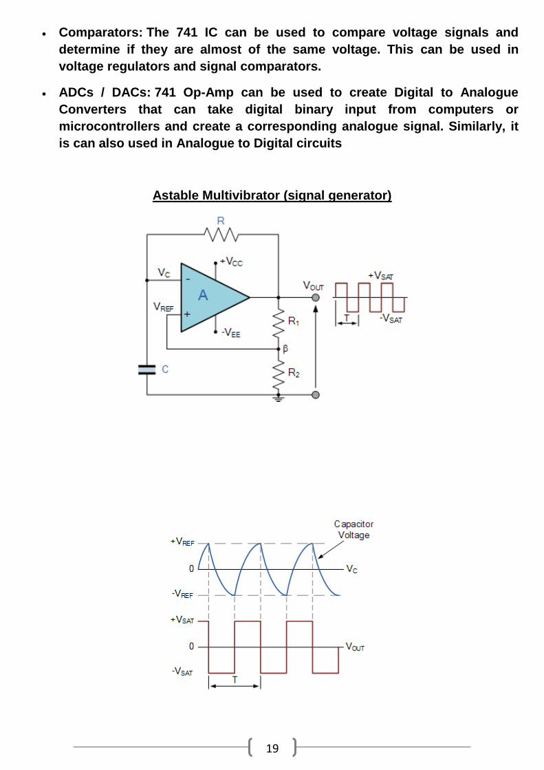
Astable Multivibrator (signal generator)
20
Once the op-amps inverting terminal reaches the new negative reference voltage, -Vref at the non-inverting terminal, the op-amp once again changes state and the output is driven to the opposing supply rail voltage, +V(sat). The capacitor now see’s a positive voltage across its plates and the charging cycle begins again. Thus, the capacitor is constantly charging and discharging creating an astable op-amp multivibrator output.
The period of the output waveform is determined by the RC time constant of the two timing components and the feedback ratio established by the R1, R2 voltage divider network which sets the reference voltage level. If the positive and negative values of the amplifiers saturation voltage have the same magnitude, then t1 = t2 and the expression to give the period of oscillation becomes:
Ex1: in the previous circuit if Ra=Rb=R=10kΩ and C=0.1μF, calculate Vb if
Vout=±12V, then find frequency of output voltage.
Ex1: An op-amp multivibrator circuit is constructed using the following
components. R1 = 35kΩ, R2 = 30kΩ, R = 50kΩ and C = 0.01uF. Calculate the
circuits frequency of oscillation.
21
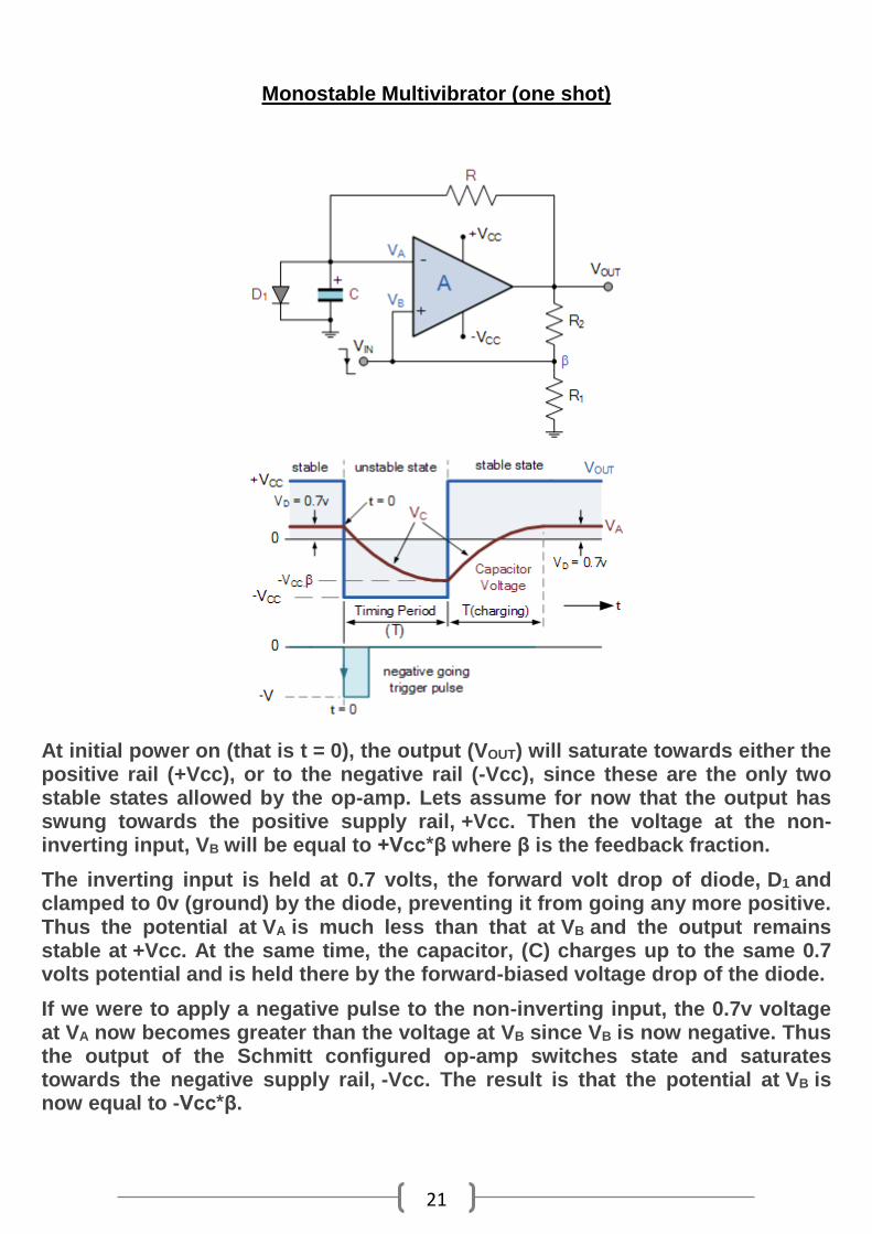
Monostable Multivibrator (one shot)
At initial power on (that is t = 0), the output (VOUT) will saturate towards either the positive rail (+Vcc), or to the negative rail (-Vcc), since these are the only two stable states allowed by the op-amp. Lets assume for now that the output has swung towards the positive supply rail, +Vcc. Then the voltage at the non-inverting input, VB will be equal to +Vcc*β where β is the feedback fraction.
The inverting input is held at 0.7 volts, the forward volt drop of diode, D1 and clamped to 0v (ground) by the diode, preventing it from going any more positive. Thus the potential at VA is much less than that at VB and the output remains stable at +Vcc. At the same time, the capacitor, (C) charges up to the same 0.7 volts potential and is held there by the forward-biased voltage drop of the diode.
If we were to apply a negative pulse to the non-inverting input, the 0.7v voltage at VA now becomes greater than the voltage at VB since VB is now negative. Thus the output of the Schmitt configured op-amp switches state and saturates towards the negative supply rail, -Vcc. The result is that the potential at VB is now equal to -Vcc*β.
22
This temporary meta-stable state causes the capacitor to charge up exponentially in the opposite direction through the feedback resistor, R from +0.7 volts down to the saturated output which it has just switched too, -Vcc. Diode, D1 becomes reverse-biased so has no effect. The capacitor, C will discharge at a time constant τ = RC.
As soon as the capacitor voltage at VA reaches the same potential as VB, that is -Vcc*β, the op-amp switches back to its original permanent stable state with the output saturated once again at +Vcc.
Note that once the timing period is complete and the op-amps output changes back to its stable state and saturates towards the positive supply rail, the capacitor tries to charge up in reverse to +Vcc but can only charge to a maximum value of 0.7v given by the diodes forward voltage drop. We can show this effect graphically as
Then we can see that a negative-going trigger input, will switch the op-amp monostable circuit into its temporary unstable state. After a time delay, T while the capacitor, Ccharges up through the feedback resistor, R, the circuit switches back to its normal stable state once the capacitor voltage reaches the required potential.
This time delay period (T) of the rectangular pulse at the output, the unstable state time, is given as:
Comparator
Zero crossing detector……
Thyristor
It is a multi-layer semiconductor device, The thyristor is a three-terminal
device labelled: “Anode”, “Cathode” and “Gate” and consisting of three PN
junctions which can be switched “ON” and “OFF”, and is represented by the
symbol as shown.
23
Like the diode, the Thyristor is a unidirectional device, that is it will only conduct
current in one direction only, but unlike a diode, the thyristor can be made to
operate as either an open-circuit switch or as a rectifying diode depending upon
how the thyristors gate is triggered. In other words, thyristors can operate only
in the switching mode and cannot be used for amplification.
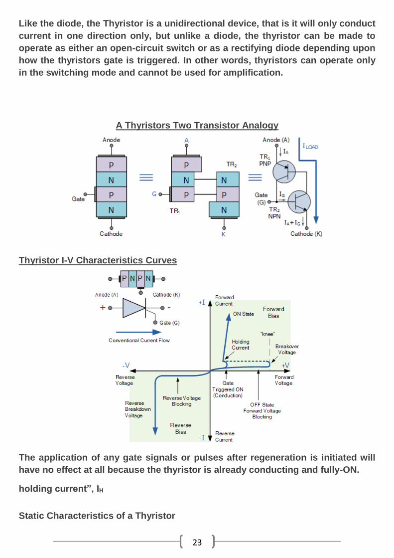
A Thyristors Two Transistor Analogy
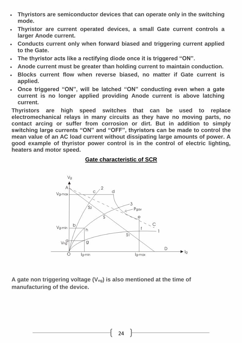
Thyristor I-V Characteristics Curves
The application of any gate signals or pulses after regeneration is initiated will
have no effect at all because the thyristor is already conducting and fully-ON.
holding current”, IH
Static Characteristics of a Thyristor
24
Thyristors are semiconductor devices that can operate only in the switching mode.
Thyristor are current operated devices, a small Gate current controls a larger Anode current.
Conducts current only when forward biased and triggering current applied to the Gate.
The thyristor acts like a rectifying diode once it is triggered “ON”.
Anode current must be greater than holding current to maintain conduction.
Blocks current flow when reverse biased, no matter if Gate current is applied.
Once triggered “ON”, will be latched “ON” conducting even when a gate current is no longer applied providing Anode current is above latching current.
Thyristors are high speed switches that can be used to replace electromechanical relays in many circuits as they have no moving parts, no contact arcing or suffer from corrosion or dirt. But in addition to simply switching large currents “ON” and “OFF”, thyristors can be made to control the mean value of an AC load current without dissipating large amounts of power. A good example of thyristor power control is in the control of electric lighting, heaters and motor speed.
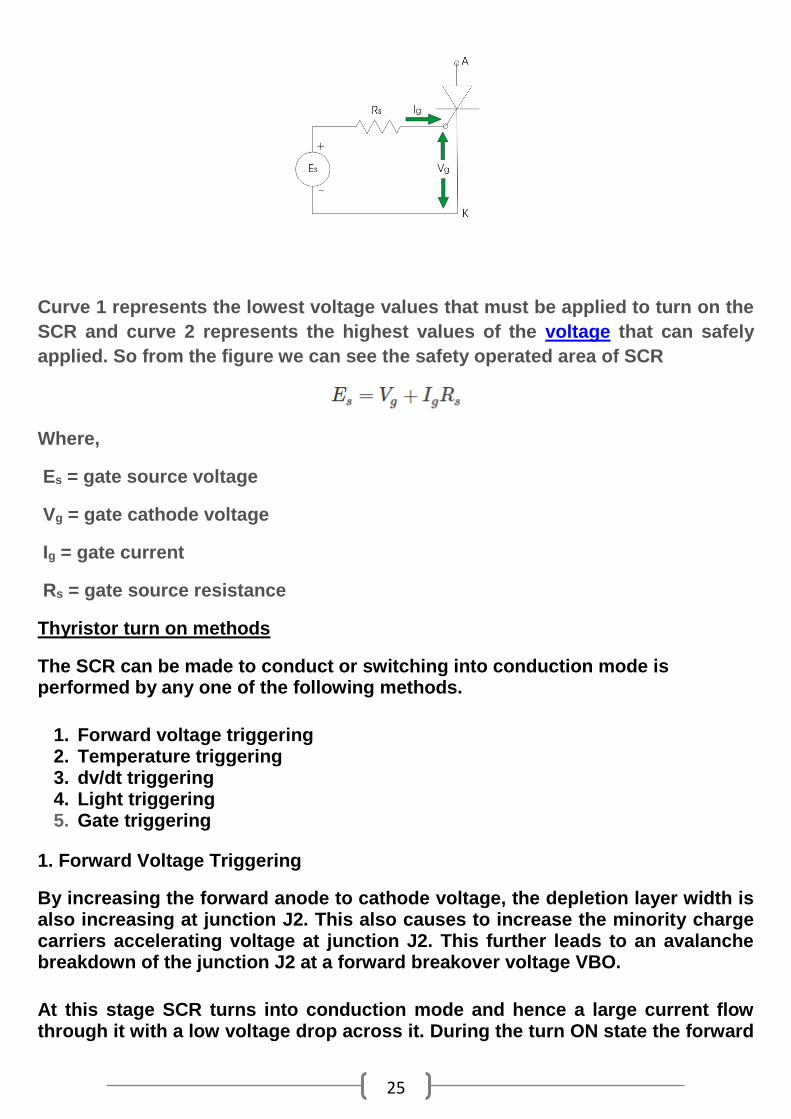
Gate characteristic of SCR
A gate non triggering voltage (Vng) is also mentioned at the time of
manufacturing of the device.
25
Curve 1 represents the lowest voltage values that must be applied to turn on the
SCR and curve 2 represents the highest values of the voltage that can safely
applied. So from the figure we can see the safety operated area of SCR
Where,
Es = gate source voltage
Vg = gate cathode voltage
Ig = gate current
Rs = gate source resistance
Thyristor turn on methods
The SCR can be made to conduct or switching into conduction mode is performed by any one of the following methods.
1. Forward voltage triggering 2. Temperature triggering 3. dv/dt triggering 4. Light triggering 5. Gate triggering
1. Forward Voltage Triggering
By increasing the forward anode to cathode voltage, the depletion layer width is also increasing at junction J2. This also causes to increase the minority charge carriers accelerating voltage at junction J2. This further leads to an avalanche breakdown of the junction J2 at a forward breakover voltage VBO.
At this stage SCR turns into conduction mode and hence a large current flow through it with a low voltage drop across it. During the turn ON state the forward

26
voltage drop across the SCR is in the range of 1 to 1.5 volts and this may be increased with the load current.
In practice this method is not employed because it needs a very large anode to cathode voltage. And also once the voltage is more than the VBO, it generates very high currents which may cause damage to the SCR. Therefore, most of the cases this type of triggering is avoided.
2. Temperature Triggering
The reverse leakage current depends on the temperature. If the temperature is increased to a certain value, the number of hole-pairs also increases. This causes to increase the leakage current and further it increases the current gains of the SCR. This starts the regenerative action inside the SCR since the (α1 + α2) value approaches to unity (as the current gains increases).
By increasing the temperature at junction J2 causes the breakdown of the junction and hence it conducts. This triggering occur in some circumstances particularly when it the device temperature is more (also called false triggering). This type of triggering is practically not employed because it causes the thermal runaway and hence the device or SCR may be damaged.
Back to top
3. dv/dt Triggering
In forward blocking state junctions J1 and J3 are forward biased and J2 is reverse biased. So the junction J2 behaves as a capacitor (of two conducting plates J1 and J3 with a dielectric J2) due to the space charges in the depletion region. The charging current of the capacitor is given as
I = C dv/ dt
where dv/dt is the rate of change of applied voltage and C is the junction capacitance.
From the above equation, if the rate of change of the applied voltage is large that leads to increase the charging current which is enough to increase the value of alpha. So the SCR becomes turned ON without a gate signal.
However, this method is also practically avoided because it is a false turn ON process and also this can produce very high voltage spikes across the SCR so there will be considerable damage to it.
27
4. Light Triggering
An SCR turned ON by light radiation is also called as Light Activated SCR (LASCR). This type of triggering is employed for phase controlled converters in HVDC transmission systems. In this method, light rays with appropriate wavelength and intensity are allowed to strike the junction J2.
These types of SCRs are consisting a niche in the inner p-layer. Therefore, when the light struck on this niche, electron-hole pairs are generated at the junction J2 which provides additional charge carriers at the junction leads to turn ON the SCR.
5.Gate Triggering
This is most common and efficient method to turn ON the SCR. When the SCR is forward biased, a sufficient voltage at the gate terminal injects some electrons into the junction J2. This result to increase reverse leakage current and hence the breakdown of junction J2 even at the voltage lower than the VBO.
Depends on the size of the SCR the gate current varies from a few milli-amps to 200 milli amps or more. If the gate current applied is more, then more electrons are injected into the junction J2 and results to come into the conduction state at much lower applied voltage.
In gate triggering method, a positive voltage applied between the gate and the cathode terminals. We can use three types of gate signals to turn On the SCR. Those are DC signal, AC signal and pulse signal.
Dynamic Turn ON Switching Characteristics
The dynamic processes of the SCR are turn ON and turn OFF processes in which both voltage and currents of an SCR vary with time. The transition from one state to another takes finite time, but doesn’t take place instantaneously.
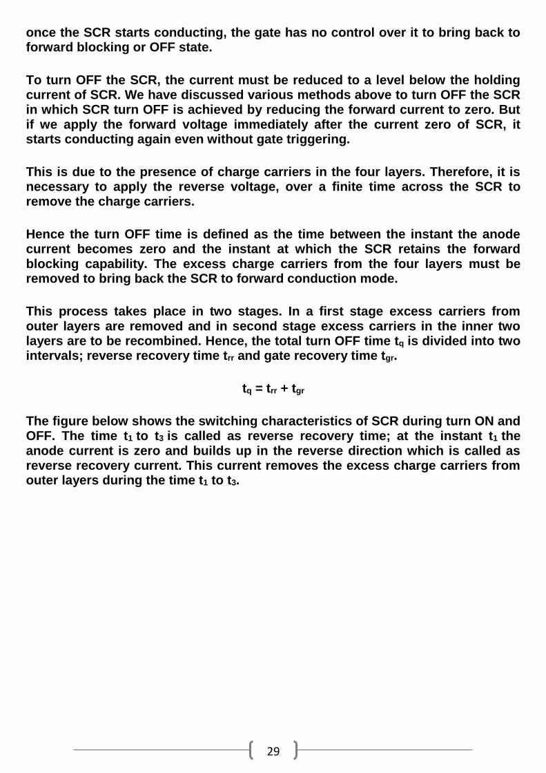
There will be a finite transition time that SCR takes to reach the forward conduction mode from blocking mode, which is termed as turn ON time of SCR. The turn ON time of the SCR Ton can be subdivided into three distinct intervals namely delay time td, rise time tr, and spread time ts.
Delay Time (td)
Rise Time (tr)
Spread Time (ts)
This is the time taken by the anode current to rise from 0.9Ia to Ia. Also the time required for the forward blocking voltage to fall from o.1Va to its ON-state

28
voltage drop which is the range of 1 to 1.5 volts. During this time anode current spread over the entire conducting region of an SCR from a narrow
Ton = tr + td + ts
Dynamic Turn OFF Switching Characteristics
The transition of an SCR from forward conduction state to forward blocking state is called as turn OFF or commutation of SCR. As we know that
29
once the SCR starts conducting, the gate has no control over it to bring back to forward blocking or OFF state.
To turn OFF the SCR, the current must be reduced to a level below the holding current of SCR. We have discussed various methods above to turn OFF the SCR in which SCR turn OFF is achieved by reducing the forward current to zero. But if we apply the forward voltage immediately after the current zero of SCR, it starts conducting again even without gate triggering.
This is due to the presence of charge carriers in the four layers. Therefore, it is necessary to apply the reverse voltage, over a finite time across the SCR to remove the charge carriers.
Hence the turn OFF time is defined as the time between the instant the anode current becomes zero and the instant at which the SCR retains the forward blocking capability. The excess charge carriers from the four layers must be removed to bring back the SCR to forward conduction mode.
This process takes place in two stages. In a first stage excess carriers from outer layers are removed and in second stage excess carriers in the inner two layers are to be recombined. Hence, the total turn OFF time tq is divided into two intervals; reverse recovery time trr and gate recovery time tgr.
tq = trr + tgr
The figure below shows the switching characteristics of SCR during turn ON and OFF. The time t1 to t3 is called as reverse recovery time; at the instant t1 the anode current is zero and builds up in the reverse direction which is called as reverse recovery current. This current removes the excess charge carriers from outer layers during the time t1 to t3.
30
Triac and its characteristics and diac
Speed control of AC motor by triac
commutation
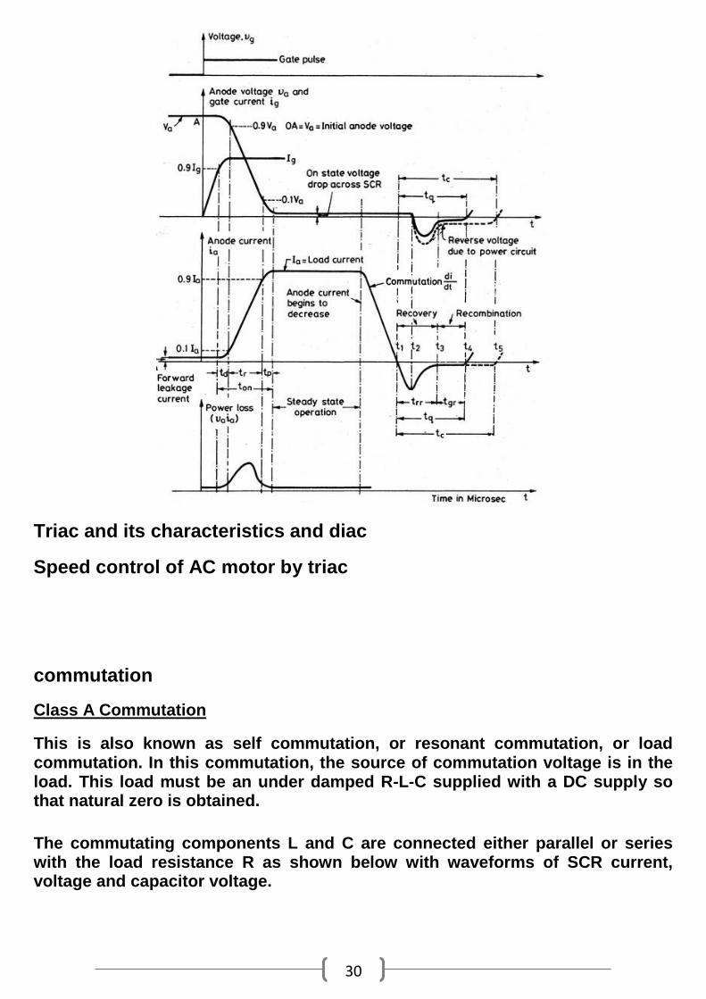
Class A Commutation
This is also known as self commutation, or resonant commutation, or load commutation. In this commutation, the source of commutation voltage is in the load. This load must be an under damped R-L-C supplied with a DC supply so that natural zero is obtained.
The commutating components L and C are connected either parallel or series with the load resistance R as shown below with waveforms of SCR current, voltage and capacitor voltage.

31
Class B Commutation
This is also a self commutation circuit in which commutation of SCR is achieved automatically by L and C components, once the SCR is turned ON. In this, the LC resonant circuit is connected across the SCR but not in series with load as in case of class A commutation and hence the L and C components do not carry the load current.
Class C Commutation
In this commutation method, the main SCR is to be commutated is connected in series with the load and an additional or complementary SCR is connected in parallel with main SCR. This method is also called as complementary commutation.
In this , SCR turns OFF with a reverse voltage of a charged capacitor. The figure below shows the complementary commutation with appropriate waveforms.
32
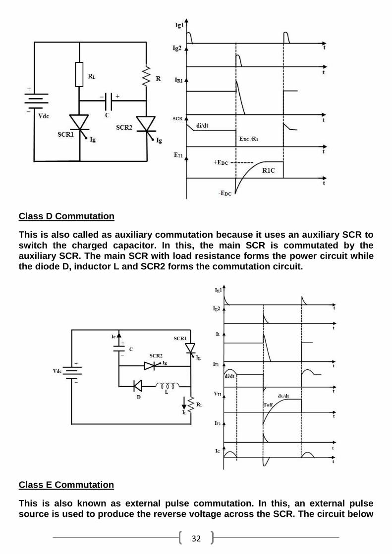
Class D Commutation
This is also called as auxiliary commutation because it uses an auxiliary SCR to switch the charged capacitor. In this, the main SCR is commutated by the auxiliary SCR. The main SCR with load resistance forms the power circuit while the diode D, inductor L and SCR2 forms the commutation circuit.
Class E Commutation
This is also known as external pulse commutation. In this, an external pulse source is used to produce the reverse voltage across the SCR. The circuit below
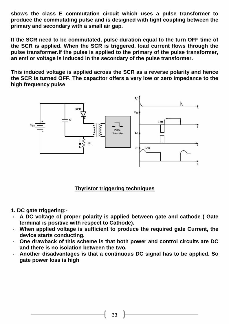
33
shows the class E commutation circuit which uses a pulse transformer to produce the commutating pulse and is designed with tight coupling between the primary and secondary with a small air gap.
If the SCR need to be commutated, pulse duration equal to the turn OFF time of the SCR is applied. When the SCR is triggered, load current flows through the pulse transformer.If the pulse is applied to the primary of the pulse transformer, an emf or voltage is induced in the secondary of the pulse transformer.
This induced voltage is applied across the SCR as a reverse polarity and hence the SCR is turned OFF. The capacitor offers a very low or zero impedance to the high frequency pulse
Thyristor triggering techniques
1. DC gate triggering:- A DC voltage of proper polarity is applied between gate and cathode ( Gate
terminal is positive with respect to Cathode). When applied voltage is sufficient to produce the required gate Current, the
device starts conducting. One drawback of this scheme is that both power and control circuits are DC
and there is no isolation between the two. Another disadvantages is that a continuous DC signal has to be applied. So
gate power loss is high

34
2. AC Gate Triggering:- Here AC source is used for gate signals. This scheme provides proper isolation between power and control circuit. Drawback of this scheme is that a separate transformer is required to step
down ac supply. There are two methods of AC voltage triggering namely (i) R Triggering (ii)
RC triggering (i) Resistance triggering: The following circuit shows the resistance triggering.
In this method, the variable resistance R is used to control the gate current. Depending upon the value of R, when the magnitude of the gate current
reaches the sufficient value(latching current of the device) the SCR starts to conduct.
The diode D is called as blocking diode. It prevents the gate cathode junction from getting damaged in the negative half cycle.
By considering that the gate circuit is purely resistive, the gate current is in phase with the applied voltage.
By using this method we can achieve maximum firing angle up to 90°.
35
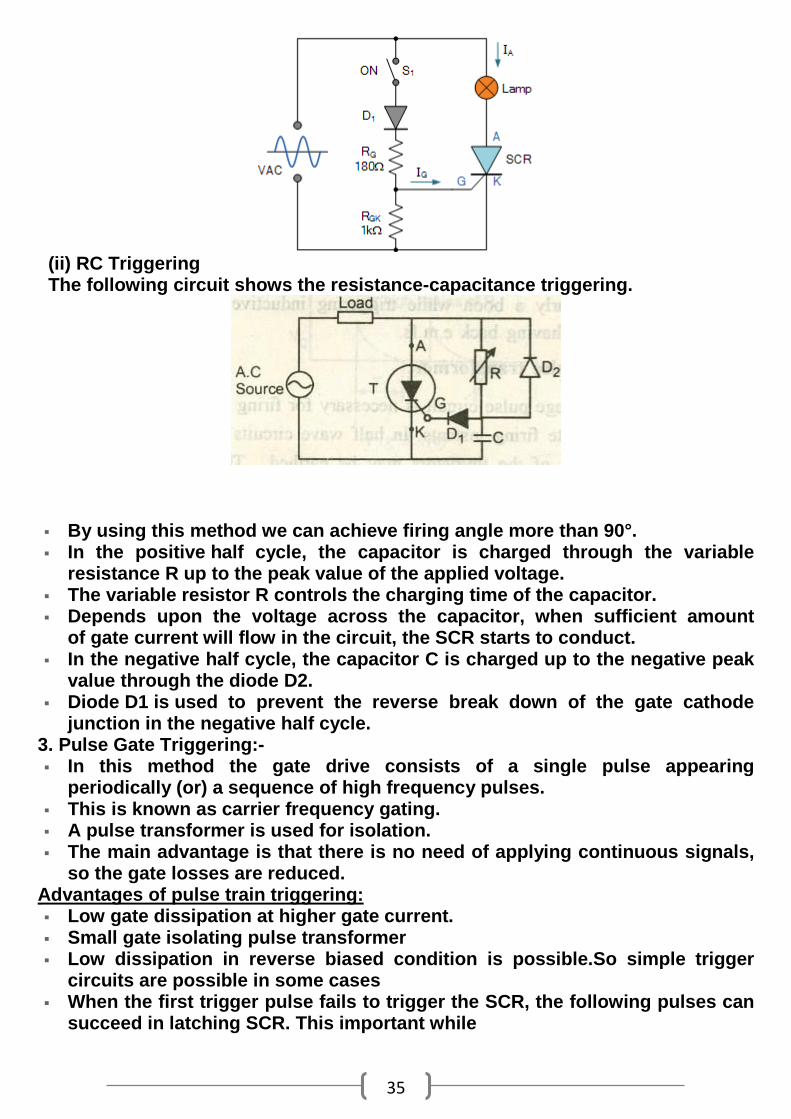
(ii) RC Triggering The following circuit shows the resistance-capacitance triggering.
By using this method we can achieve firing angle more than 90°. In the positive half cycle, the capacitor is charged through the variable
resistance R up to the peak value of the applied voltage. The variable resistor R controls the charging time of the capacitor. Depends upon the voltage across the capacitor, when sufficient amount
of gate current will flow in the circuit, the SCR starts to conduct. In the negative half cycle, the capacitor C is charged up to the negative peak
value through the diode D2. Diode D1 is used to prevent the reverse break down of the gate cathode
junction in the negative half cycle. 3. Pulse Gate Triggering:- In this method the gate drive consists of a single pulse appearing
periodically (or) a sequence of high frequency pulses. This is known as carrier frequency gating. A pulse transformer is used for isolation. The main advantage is that there is no need of applying continuous signals,
so the gate losses are reduced. Advantages of pulse train triggering: Low gate dissipation at higher gate current. Small gate isolating pulse transformer Low dissipation in reverse biased condition is possible.So simple trigger
circuits are possible in some cases When the first trigger pulse fails to trigger the SCR, the following pulses can
succeed in latching SCR. This important while
36
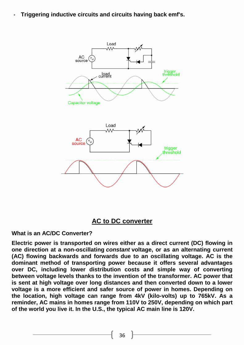
Triggering inductive circuits and circuits having back emf's.
AC to DC converter
What is an AC/DC Converter?
Electric power is transported on wires either as a direct current (DC) flowing in one direction at a non-oscillating constant voltage, or as an alternating current (AC) flowing backwards and forwards due to an oscillating voltage. AC is the dominant method of transporting power because it offers several advantages over DC, including lower distribution costs and simple way of converting between voltage levels thanks to the invention of the transformer. AC power that is sent at high voltage over long distances and then converted down to a lower voltage is a more efficient and safer source of power in homes. Depending on the location, high voltage can range from 4kV (kilo-volts) up to 765kV. As a reminder, AC mains in homes range from 110V to 250V, depending on which part of the world you live it. In the U.S., the typical AC main line is 120V.
37
Converters steer an alternating current, as its voltage also alternates, into reactive impedance elements, such as inductors (L) and capacitors (C), where it is stored and integrated. This process separates the power associated with the positive and negative potentials. Filters are used to smooth out the energy stored, resulting in creation of a DC source for other circuits
Applications:
Speed control of DC motor in DC drives.
• UPS.
• HVDC transmission.
• Battery Chargers
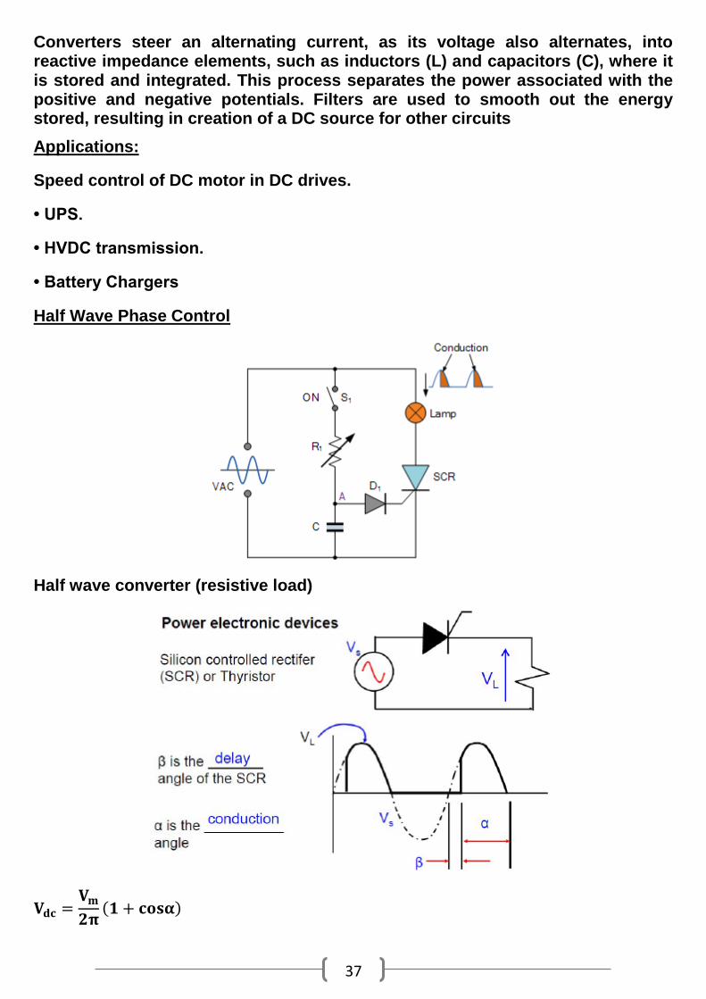
Half Wave Phase Control
Half wave converter (resistive load)
𝐕𝐝𝐜 =𝐕𝐦
𝟐𝛑(𝟏 + 𝐜𝐨𝐬𝛂)

38
𝐕𝐫𝐦𝐬 =𝐕𝐦
𝟐√
(𝛑 − 𝛂 + 𝟎. 𝟓𝐬𝐢𝐧𝟐𝛂)
𝛑
𝐏. 𝐅 =𝑷𝒐(𝒓𝒎𝒔)
𝐏𝐢𝐧(𝐕𝐀)
𝑽𝒔𝒄𝒓 =𝐕𝐦
𝟐𝛑(𝟏 − 𝐜𝐨𝐬𝛂)
Half wave converter inductive load)

39
Ex2: a small 10Ω heater, it is supplied through half wave converter, with mains
of 240V, calculate the following if α=π/3:
1. Vdc
2. Po(rms)
3. P.F
4. Vscr
And draw the waveforms.
𝐕𝐝𝐜 =𝐕𝐦
𝟐𝛑(𝟏 + 𝐜𝐨𝐬𝛂) =
𝟐𝟒𝟎√𝟐
𝟐𝛑(𝟏 + 𝐜𝐨𝐬𝟔𝟎) = 𝟖𝟏𝐕
𝐏𝐨 =𝐕𝐎(𝐫𝐦𝐬)
𝟐
𝐑𝐋
𝐕𝐫𝐦𝐬 =𝐕𝐦
𝟐√
(𝛑 − 𝛂 + 𝟎. 𝟓𝐬𝐢𝐧𝟐𝛂)
𝛑
𝐕𝐫𝐦𝐬 =𝟐𝟒𝟎 × √𝟐
𝟐√
(𝛑 −𝛑
𝟐+ 𝟎. 𝟓𝐬𝐢𝐧𝟏𝟐𝟎)
𝛑= 𝟏𝟓𝟐. 𝟐𝐕
𝐏𝐨 =(𝟏𝟓𝟐. 𝟐)𝟐
𝟏𝟎= 𝟐𝟑𝟏𝟔. 𝟒𝐤𝐰
𝐏. 𝐅 =𝑷𝒐(𝒓𝒎𝒔)
𝐏𝐢𝐧(𝐕𝐀)
𝐈𝐨(𝐫𝐦𝐬) =𝑽𝒐(𝒓𝒎𝒔)
𝐑𝐋=
𝟏𝟓𝟐. 𝟐
𝟏𝟎= 𝟏𝟓. 𝟐𝟐𝐀
𝐏𝐢𝐧=𝟐𝟒𝟎×𝟏𝟓.𝟐𝟐=𝟑.𝟔𝟓𝟐𝟖𝐤𝐰
𝐏. 𝐅 =𝟐. 𝟑𝟏𝟔
𝟑. 𝟔𝟓𝟐𝟖= 𝟎. 𝟔𝟑𝟒
𝑽𝒔𝒄𝒓 =𝐕𝐦
𝟐𝛑(𝟏 − 𝐜𝐨𝐬𝛂) =
𝟐𝟒𝟎√𝟐
𝟐𝛑(𝟏 − 𝐜𝐨𝐬𝟔𝟎) = 𝟐𝟕𝐕

40
Load with DC back e.m.f.:
Ex1: resistive load with back e.m.f. dc source in series of 170V, the supply AC of
240V. Calculate α limits for possible triggering.
𝜹 ≤ 𝛂 ≤ 𝛑 − 𝛅
𝛅 = 𝐬𝐢𝐧−𝟏(𝐕𝐛
𝐕𝐦)
𝛅 = 𝐬𝐢𝐧−𝟏 (𝟏𝟕𝟎
𝟐𝟒𝟎√𝟐) = 𝟑𝟎𝟎
𝛑 − 𝛅 = 𝟏𝟖𝟎 − 𝟑𝟎 = 𝟏𝟓𝟎𝟎
𝟑𝟎𝟎 ≤ 𝛂 ≤ 𝟏𝟓𝟎𝟎
Fully controlled bridge converter with inductive load
Ex1: resistive load (30Ω) is supplied from half controlled bridge converter,
calculate rms, value for load voltage and load current at α=300 . the supply
voltage is 230V.
𝐕𝐫𝐦𝐬 =𝐕𝐦
√𝟐√
𝛑 − 𝛂 + 𝟎. 𝟓𝐬𝐢𝐧𝟐𝛂
𝛑
𝐕𝐫𝐦𝐬 =𝟐𝟑𝟎√𝟐
√𝟐√
𝛑 −𝛑
𝟔+ 𝟎. 𝟓𝐬𝐢𝐧
𝛑
𝟔
𝛑
𝐈𝐨(𝐫𝐦𝐬) =𝐕𝐨(𝐫𝐦𝐬)
𝐑𝐋=
𝟐𝟐𝟔. 𝟔
𝟑𝟎= 𝟕. 𝟓𝟓𝐀
Ex2: half controlled bridge converter supplied field power to DC motor, the field
coils have L=0.1H and R=100Ω, what is the triggering angle α if If=1.8A and
source voltage is 220V.
𝐕𝐟 = 𝐈𝐟 × 𝐑𝐟 = 𝟏. 𝟖 × 𝟏𝟎𝟎 = 𝟏𝟖𝟎𝐕
𝐕𝐝𝐜 =𝟐𝐕𝐦
𝛑× 𝐜𝐨𝐬𝛂

41
𝐜𝐨𝐬𝛂 =𝐕𝐝𝐜 × 𝛑
𝟐𝐕𝐦=
𝟏𝟖𝟎 × 𝟑 × 𝟏. 𝟒𝟏𝟔
𝟐 × √𝟐 × 𝟐𝟒𝟎= 𝟎. 𝟗𝟎𝟖𝟕
𝛂 = 𝐜𝐨𝐬−𝟏(𝟎. 𝟒𝟎𝟖𝟕) = 𝟐𝟒. 𝟔𝟔𝟎
Ex3: fully controlled converter as given before with L=50mH, R=10Ω,
α=30o,V=325sin100πt, calculate: 1.Vdc 2.Փ 3.time necessary to commutate the
thyristor, 4.what could be the current wave forms.
𝐕𝐝𝐜 = 𝐕𝐨 =𝟐𝐕𝐦
𝛑× 𝐜𝐨𝐬 ∝=
𝟐 × 𝟑𝟐𝟓
𝛑𝐜𝐨𝐬𝟑𝟎 = 𝟏𝟕𝟗. 𝟐𝐕
𝛗 = 𝐭𝐚𝐧−𝟏𝐰𝐋
𝐑
= 𝐭𝐚𝐧−𝟏𝟏𝟎𝟎 × 𝟏𝟓𝟎 × 𝟏𝟎−𝟑
𝟏𝟎= 𝟓𝟕. 𝟓𝐨
Time for commutation thyristor is 𝛑 − 𝛂 = 𝐰𝐭
𝐭𝐪 =𝛑 − 𝛂
𝐰=
𝛑 −𝛑
𝟔
𝟏𝟎𝟎𝛑= 𝟖. 𝟑𝟑𝐦𝐬
Since ᵠ˃α the current will continue to conduct
Ex4: for this circuit if L˃˃R, calculate Vdcwith and without free wheeling diode,
α=45o.
𝐕𝟏
𝐕𝟐=
𝐍𝟏
𝐍𝟐=
𝟐
𝟏
𝐕𝟐 =𝐕𝟏
𝐍𝟏/𝐍𝟐 =
𝟐𝟒𝟎
𝟐= 𝟏𝟐𝟎
𝐕𝐚 = 𝐕𝐛 =𝟏
𝟐𝐕𝟐 = 𝟔𝟎
In case of existence of free wheeling diode:
𝐕𝐝𝐜 =𝐕𝐦
𝛑× (𝟏 + 𝐜𝐨𝐬𝛂)
=𝟔𝟎√𝟐
𝛑× (𝟏 + 𝐜𝐨𝐬𝟒𝟓) = 𝟒𝟓. 𝟔𝟔𝐕
In case of absense of free wheeling diode:
𝐕𝐝𝐜 =𝐕𝐦
𝛑× (𝐜𝐨𝐬𝛂 − 𝐜𝐨𝐬𝛄)

42
𝛄 = 𝛑 + 𝛂 = 𝟏𝟖𝟎 + 𝟒𝟓 = 𝟐𝟐𝟓
𝐕𝐝𝐜 =𝟔𝟎√𝟐
𝛑× (𝐜𝐨𝐬𝟒𝟓 − 𝐜𝐨𝐬𝟐𝟐𝟓) = 𝟑𝟖. 𝟏𝟗𝐕
Ex3: for this circuit if Vs=350sin315t, the conducting time for each thyristor is
(2.5ms), find: 1. Vo(rms) 2. Po(rms)
to find α we calculate F&T.
ω=315 ω=2πf
𝐟 =𝛚
𝟐𝛑=
𝟑𝟏𝟓
𝟐𝛑= 𝟓𝟎𝐇𝐳
𝐓 =𝟏
𝐟= 𝟐𝟎𝐦𝐬
𝛃 =𝟐. 𝟓
𝟐𝟎× 𝟑𝟔𝟎𝟎 = 𝟒𝟓𝟎 =
𝛑
𝟒
𝛂 = 𝛑 − 𝛃 = 𝛑 −𝛑
𝟒=
𝟑𝛑
𝟒
𝐕𝐫𝐦𝐬 =𝐕𝐦
√𝟐× √
𝛑 − 𝛂 + 𝟎. 𝟓𝐬𝐢𝐧𝟐𝛂
𝛑
𝐕𝐫𝐦𝐬 =𝟑𝟓𝟎
√𝟐× √
𝛑 −𝟑𝛑
𝟒+ 𝟎. 𝟓𝐬𝐢𝐧𝟐 ×
𝟑𝛑
𝟒
𝛑= 𝟕𝟓. 𝟑𝐕
𝐏𝐨(𝐫𝐦𝐬) =𝐕(𝐫𝐦𝐬)
𝟐
𝐑𝐥=
(𝟕𝟓. 𝟑)𝟐
𝟕= 𝟐𝟏𝟎𝐕
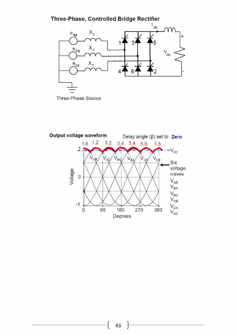
Three phase AC to DC converter:
43
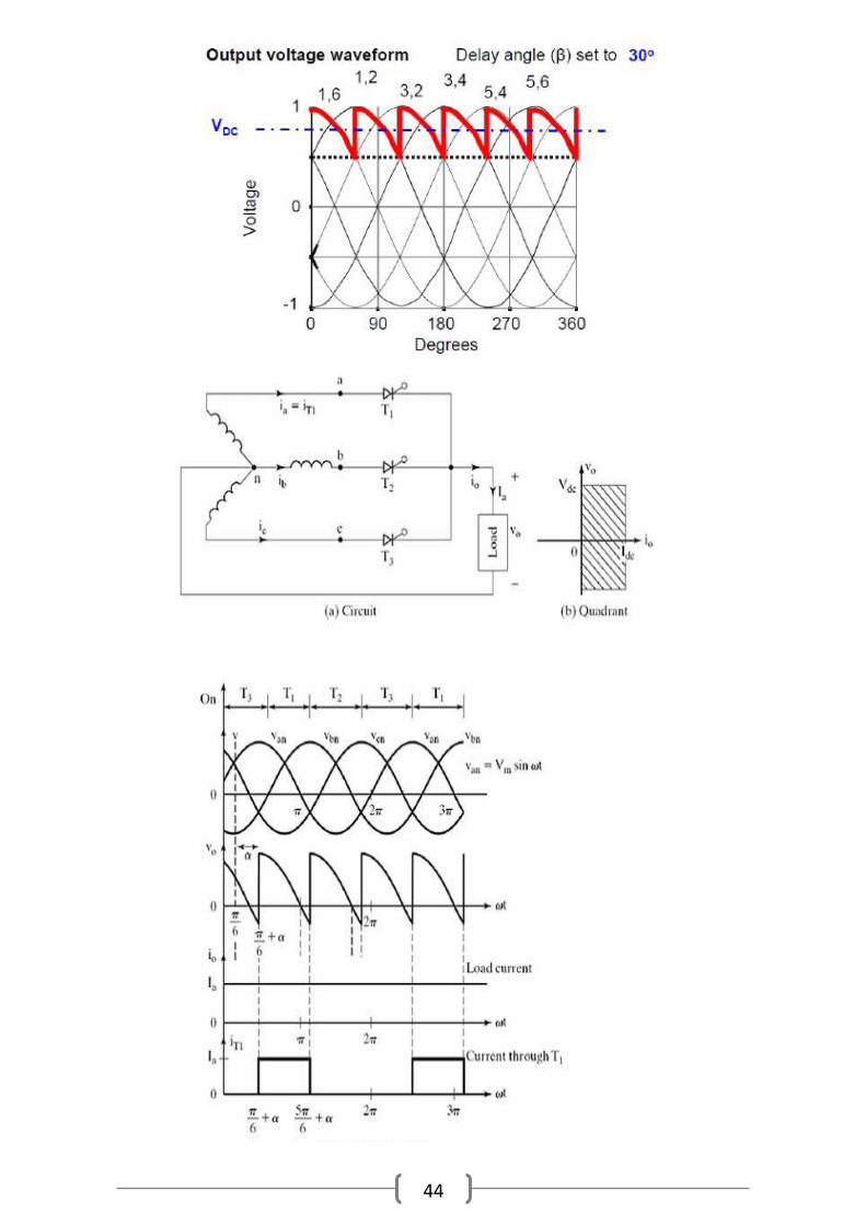
44
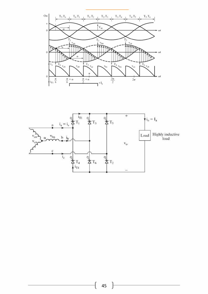
45
46
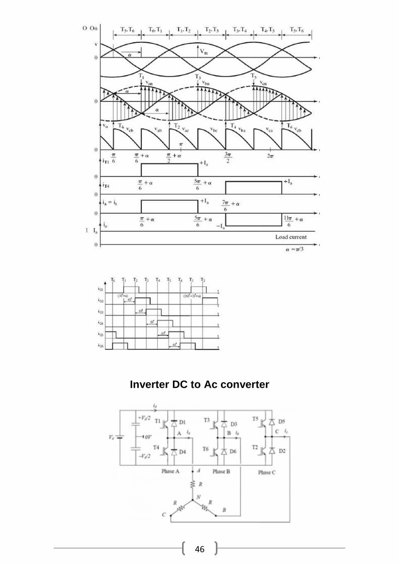
Inverter DC to Ac converter

47
Applications of a 3-phase square wave inverter
(i) A low cost solid-state frequency changer circuit: This circuit converts the 3-
phase ac (input) voltages of one frequency to 3-phase ac (output) voltages of the
desired frequency. The input ac is first converted into dc and then converted
back to ac of new frequency. The square wave inverter discussed in this lesson
may be used for dc to ac conversion. Such a circuit may, for example, convert 3-
phase ac voltages of 50 Hz to 3-phase ac voltages of 60 Hz. The input to this
circuit could as well have come from a single-phase supply, in which case the
single-phase ac is first converted into dc and then converted back to 3-phase ac
of the desired frequency.
(ii) An uninterrupted power supply circuit: Uninterrupted power supply circuits
are used to provide uninterrupted power to some critical load. Here a critical
load requiring 3-phase ac supply of fixed magnitude and frequency has been
considered. In case ac mains supply fails, the 3-phase load may be electronically
switched, within few milliseconds, to the output of the 3-phase square wave
inverter. Input dc supply of the inverter often comes from a battery bank.
Limitations of 3-Phase Square Wave Inverter:
. In spite of the inherent low-pass filtering property of the motor load, the load
current may still contain some harmonics. These harmonic currents cause extra
iron and copper losses in the motor. They also produce unwanted torque
pulsations. Fortunately the torque pulsations due to harmonic currents are of
high frequencies and their effect gets subdued due to the large mechanical
inertia of the drive system. The motor speed hardly changes in response to
these torque pulsations.
However in some cases torque pulsations of particular frequencies may cause
unwanted resonance in the mechanical system of the drive. A special notch filter
may then be required to remove these frequencies from the inverter output
voltage. The input dc voltage to the inverter is often derived from an ac source
after rectification and filtering. A simple diode bridge rectifier followed by a filter
capacitor is often the most cost-effective method to get dc voltage from ac
supply. In some applications, like in un-interrupted power supplies, the dc input
may be coming from a bank of batteries. In both these examples, the input dc
magnitude is fairly constant. With fixed input dc voltage the square-wave
inverter can output only fixed magnitude of load voltage. This does not suit the
requirement in many cases where the load requires a variable voltage variable
frequency (VVVF) supply. In order that ac output voltage magnitude is
controllable, the inverter input voltage will need to be varied using an additional
dc-to-dc converter. However a better solution will be to use a PWM inverter
48
which can provide a VVVF output with enhanced output voltage quality. In spite
of the limitations, discussed above, the square wave inverter may be a preferred
choice on account of its simplicity and low cost. The switch control circuit is
very simple and the switching frequency is significantly lower than in PWM
inverters.
This results in low switching losses. The switch cost may also be lower as one
may do away with slower switching devices and slightly lower rated switches.
Another advantage over PWM inverter is its ability to output higher magnitude of
fundamental voltage than the maximum that can be output from a PWM inverter.
Parallel inverter:
𝑽𝑳 = 𝑽𝒂𝟏 + 𝑽𝒂𝟐
𝒇𝒎𝒂𝒙 =𝒏𝟐
𝟒𝟖𝑪𝑹𝑳
𝟎. 𝟐𝟓 <𝒕𝒐𝒏
𝒕𝒐𝒇𝒇< 3.34
𝒕𝒐𝒏 =𝟒𝑪𝑹𝑳
𝒏𝟐
𝒕𝒐𝒇𝒇 =𝑳𝒏𝟐
𝑹𝑳
Ex1: Design parallel inverter to give 400Hz square wave suppling120W resistive
load at 240V, the DC voltage is 12V.
𝑷 =𝑽𝒔
𝟐
𝑹𝑳
𝑹𝑳 =𝑽𝒔
𝟐
𝑷 =
𝟐𝟒𝟎𝟐
𝟏𝟐𝟎 = 𝟒𝟖𝟎𝛀
𝐧 =𝑽𝟏
𝑽𝟐=
𝟐𝟒𝟎
𝟏𝟐= 𝟐𝟎
𝒇𝒎𝒂𝒙 =𝒏𝟐
𝟒𝟖𝑪𝑹𝑳
𝑪 =𝒏𝟐
𝟒𝟖𝒇𝒎𝒂𝒙𝑹𝑳 =
𝟐𝟎𝟐
𝟒𝟖𝟎 × 𝟒𝟎𝟎 × 𝟒𝟖𝟎= 𝟒𝟑𝝁𝑭
𝒕𝒐𝒏 = 𝟐𝒕𝒒
49
𝒕𝒒 =𝒕𝒐𝒏
𝟐 =
𝟏𝟒𝑪𝑹𝑳
𝟐𝒏𝟐 =
𝟏 × 𝟒 × 𝟒𝟕 × 𝟏𝟎−𝟔 × 𝟒𝟖𝟎
𝟐 × 𝟐𝟎𝟐 = 𝟏𝟏𝟐. 𝟖𝝁𝒔
𝒕𝒐𝒏 = 𝟑𝒕𝒐𝒇𝒇𝒕𝒐𝒇𝒇 =𝒕𝒐𝒏
𝟑
𝒕𝒐𝒇𝒇 =𝑳 × 𝒏𝟐
𝑹𝑳=
𝟒𝑪 × 𝑹𝑳
𝟑 × 𝒏𝟐
𝑳 =𝟒𝑪 × 𝑹𝑳 × 𝑹𝑳
𝟑 × 𝒏𝟐 × 𝒏𝟐 =
𝟒 × 𝟒𝟕 × 𝟏𝟎−𝟔 × 𝟒𝟖𝟎𝟐
𝟑 × 𝟐𝟎𝟒= 𝟗𝟎. 𝟐𝟒𝝁𝑯
Series inverter:
𝑽𝒔 =𝝅 × 𝑰𝒎 × 𝑹
𝟑
𝑳 =𝑹 × 𝝅
𝟐𝑾𝒅
𝑪 =𝟒𝑳
𝟒𝑳𝟐 × 𝑾𝒅𝟐 + 𝑹𝟐
Ex1: Design a series inverter with max current=1A, R=150Ω, f=400Hz, assuming
that tq=25μs.
𝑻 =𝟏
𝒇=
𝟏
𝟒𝟎𝟎= 𝟐𝟓𝝁𝒔
𝑻
𝟐=
𝟐. 𝟓
𝟐= 𝟏. 𝟐𝟓𝒎𝒔 = 𝟏𝟐𝟓𝟎𝝁𝒔
𝑻
𝟐= 𝒕𝒐𝒏 + 𝒕𝒐𝒇𝒇
𝒕𝒐𝒏 =𝑻
𝟐− 𝒕𝒐𝒇𝒇 = 𝟏𝟐𝟓𝟎 − 𝟐𝟓 = 𝟏𝟐𝟐𝟓𝝁𝒔
𝑾𝒅 =𝝅
𝒕𝒐𝒏=
𝝅
𝟏𝟐𝟐𝟓 × 𝟏𝟎−𝟔= 𝟐. 𝟓𝟔 × 𝟏𝟎𝟑
𝒓𝒂𝒅
𝒔
𝑽𝒔 =𝝅 × 𝑰𝒎 × 𝑹
𝟑=
𝝅 × 𝟏 × 𝟏𝟓𝟎
𝟑= 𝟏𝟓𝟕𝑽
𝑳 =𝑹 × 𝝅
𝟐𝑾𝒅=
𝟏𝟓𝟎 × 𝝅
𝟐 × 𝟐. 𝟓𝟔 × 𝟏𝟎𝟑= 𝟗𝟐𝒎𝑯
𝑪 =𝟒𝑳
𝟒𝑳𝟐 × 𝑾𝒅𝟐 + 𝑹𝟐
=𝟒 × 𝟗𝟐 × 𝟏𝟎−𝟑
𝟒(𝟗𝟐 × 𝟏𝟎−𝟑)𝟐 × (𝟐. 𝟓𝟔 × 𝟏𝟎−𝟑)𝟐 + 𝟏𝟓𝟎𝟐= 𝟏𝟓. 𝟕𝝁𝑭

50
Half bridge single phase inverter:

51
Chopper DC to DC converter
A chopper uses high speed to connect and disconnect from a source load. A
fixed DC voltage is applied intermittently to the source load by continuously
triggering the power switch ON/OFF. The period of time for which the power
switch stays ON or OFF is referred to as the chopper’s ON and OFF state times,
respectively.
Choppers are mostly applied in electric cars, conversion of wind and solar
energy, and DC motor regulators.
Symbol of a Chopper
Classification of Choppers
Depending on the voltage output, choppers are classified as −
Step Up chopper (boost converter)
Step Down Chopper(Buck converter)
Step Up/Down Chopper (Buck-boost converter)
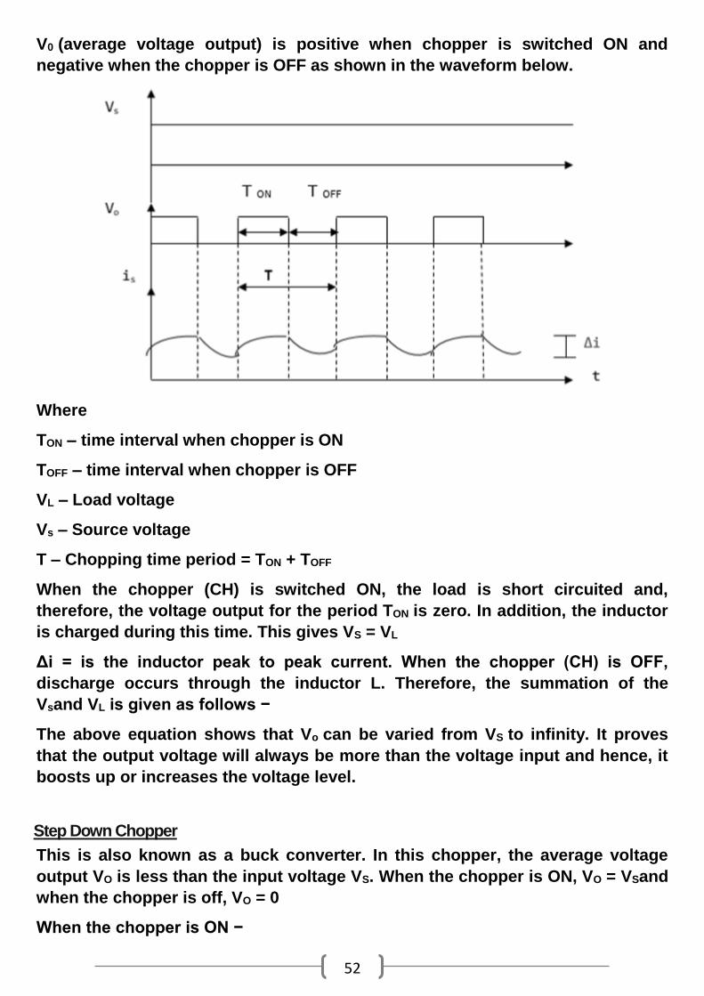
Step Up Chopper
The average voltage output (Vo) in a step up chopper is greater than the voltage
input (Vs). The figure below shows a configuration of a step up chopper.
Current and Voltage Waveforms
52
V0 (average voltage output) is positive when chopper is switched ON and
negative when the chopper is OFF as shown in the waveform below.
Where
TON – time interval when chopper is ON
TOFF – time interval when chopper is OFF
VL – Load voltage
Vs – Source voltage
T – Chopping time period = TON + TOFF
When the chopper (CH) is switched ON, the load is short circuited and,
therefore, the voltage output for the period TON is zero. In addition, the inductor
is charged during this time. This gives VS = VL
Δi = is the inductor peak to peak current. When the chopper (CH) is OFF,
discharge occurs through the inductor L. Therefore, the summation of the
Vsand VL is given as follows −
The above equation shows that Vo can be varied from VS to infinity. It proves
that the output voltage will always be more than the voltage input and hence, it
boosts up or increases the voltage level.
Step Down Chopper
This is also known as a buck converter. In this chopper, the average voltage
output VO is less than the input voltage VS. When the chopper is ON, VO = VSand
when the chopper is off, VO = 0
When the chopper is ON −

53
Circuit Diagram
Where FD is free-wheel diode.
When the chopper is OFF, polarity reversal and discharging occurs at the
inductor. The current passes through the free-wheel diode and the inductor to
the load. This gives,
Current and Voltage Waveforms
The current and voltage waveforms are given below −
For a step down chopper the voltage output is always less than the voltage
input. This is shown by the waveform below.
54
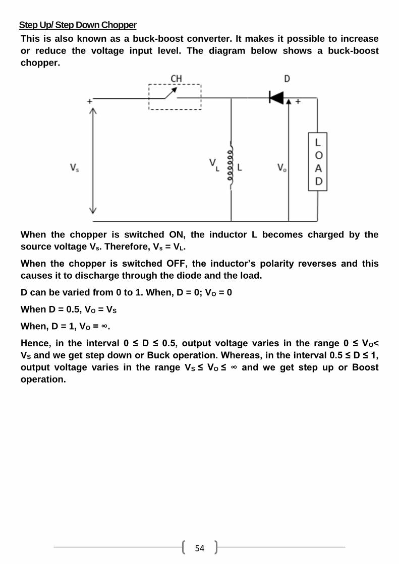
Step Up/ Step Down Chopper
This is also known as a buck-boost converter. It makes it possible to increase
or reduce the voltage input level. The diagram below shows a buck-boost
chopper.
When the chopper is switched ON, the inductor L becomes charged by the
source voltage Vs. Therefore, Vs = VL.
When the chopper is switched OFF, the inductor’s polarity reverses and this
causes it to discharge through the diode and the load.
D can be varied from 0 to 1. When, D = 0; VO = 0
When D = 0.5, VO = VS
When, D = 1, VO = ∞.
Hence, in the interval 0 ≤ D ≤ 0.5, output voltage varies in the range 0 ≤ VO<
VS and we get step down or Buck operation. Whereas, in the interval 0.5 ≤ D ≤ 1,
output voltage varies in the range VS ≤ VO ≤ ∞ and we get step up or Boost
operation.
55
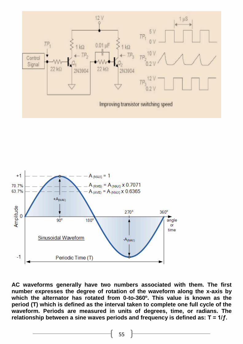
AC waveforms generally have two numbers associated with them. The first number expresses the degree of rotation of the waveform along the x-axis by which the alternator has rotated from 0-to-360o. This value is known as the period (T) which is defined as the interval taken to complete one full cycle of the waveform. Periods are measured in units of degrees, time, or radians. The relationship between a sine waves periods and frequency is defined as: T = 1/ƒ.
56
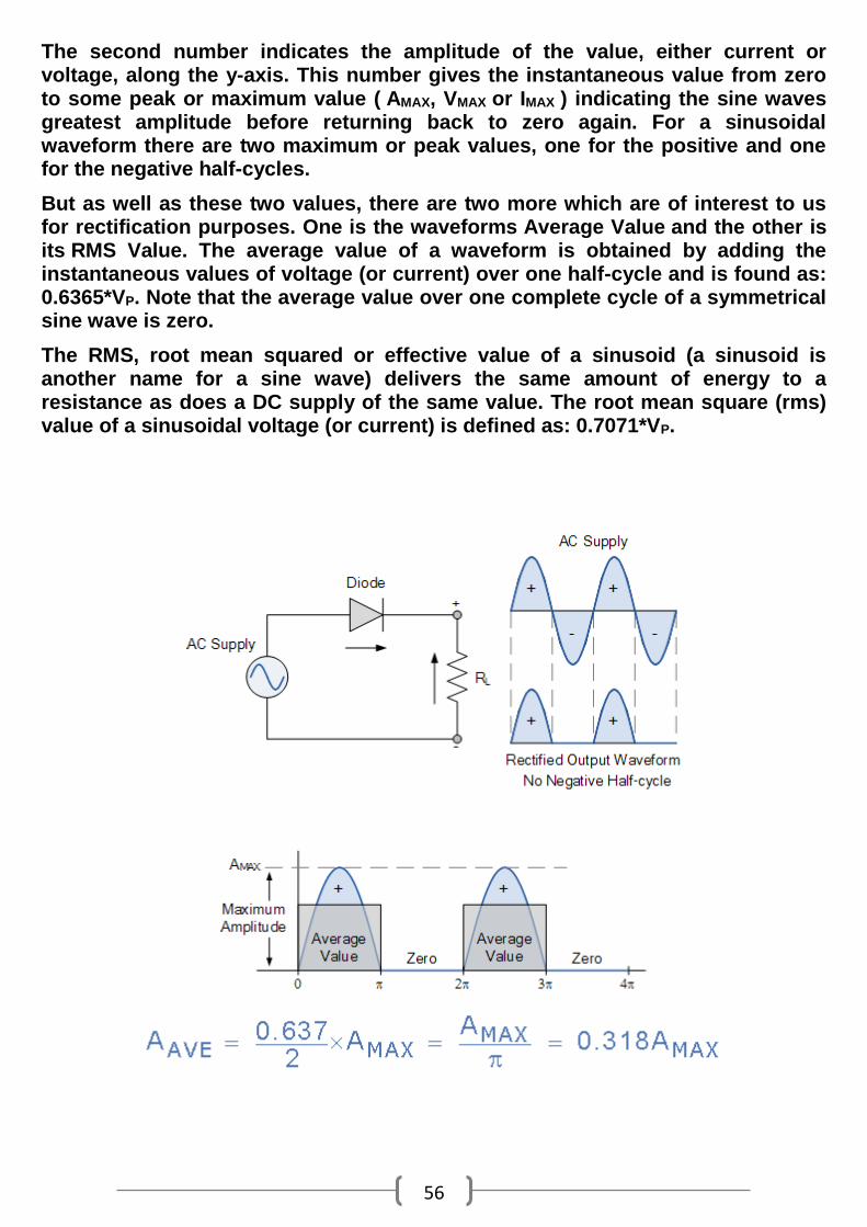
The second number indicates the amplitude of the value, either current or voltage, along the y-axis. This number gives the instantaneous value from zero to some peak or maximum value ( AMAX, VMAX or IMAX ) indicating the sine waves greatest amplitude before returning back to zero again. For a sinusoidal waveform there are two maximum or peak values, one for the positive and one for the negative half-cycles.
But as well as these two values, there are two more which are of interest to us for rectification purposes. One is the waveforms Average Value and the other is its RMS Value. The average value of a waveform is obtained by adding the instantaneous values of voltage (or current) over one half-cycle and is found as: 0.6365*VP. Note that the average value over one complete cycle of a symmetrical sine wave is zero.
The RMS, root mean squared or effective value of a sinusoid (a sinusoid is another name for a sine wave) delivers the same amount of energy to a resistance as does a DC supply of the same value. The root mean square (rms) value of a sinusoidal voltage (or current) is defined as: 0.7071*VP.
57