Embed Size (px)
Citation preview

1
47 Galaxy Avenue, Linbro Business ParkJohannesburg, South Africa
Tel: +27 11 723 6000Fax: +27 11 723 6001
Email: [email protected]: www.zest.co.za
Terms
VSD: Variable speed drive Power electronic device converting AC supply to DC, and DC to controllable AC output. Also referred to as inverters, variable frequency drives, frequency converters, etc.
LV VSD: Low voltage variable speed drive. 110 V to 690 VMV VSD: Medium voltage variable speed drive: 2300 V to 11 000 VVSI: Voltage source inverterCSI: Current source inverterGTO: Gate turn off thyristorSCR: Silicon controlled rectifier (thyristor)IGBT: Insulated gate bipolar transistorIGCT: Integrated gate commutated thyristorSGCT: Symmetrical gate commutated thyristorTHDi: Total harmonic current distortionTHDv: Total harmonic voltage distortionPWM: Pulse width modulationNPC: Neutral point clampedSOA: Safe operating areaOPP: Optimal Pulse Pattern™PTC: Positive Temperature CoefficientPCC: Point of Common CouplingAFE: Active Front EndLC: Inductor CapacitorSMPS: Switching-Mode Power Supply Circuit Design
ABSTRACT
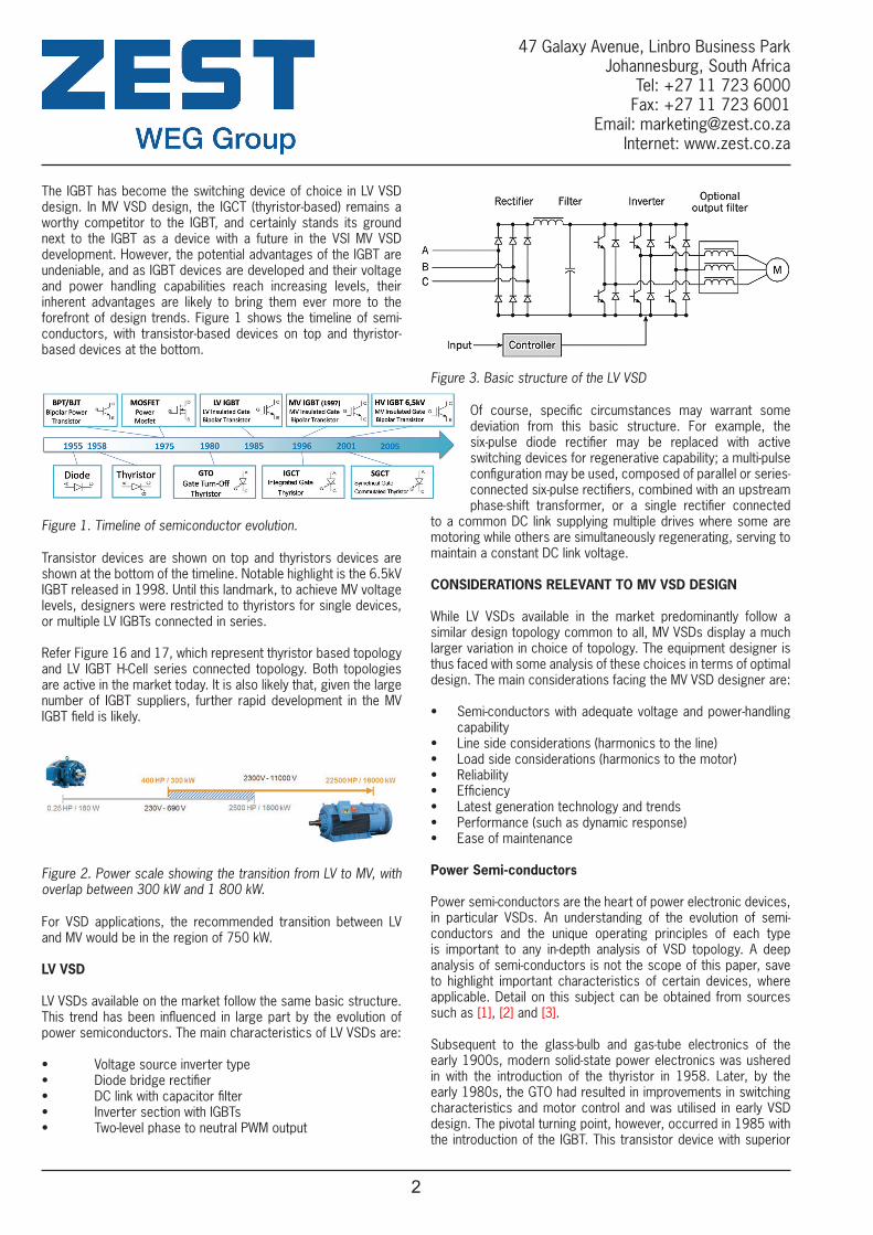
LV VSDs in the market today follow a common general topology. Power semiconductor evolution has played its role here, not least with the advent of the transistor device in the 1970s and in particular the Insulated Gate Bipolar Transistor (IGBT), commercially introduced in 1985 in low voltage (LV) format. With its superior switching characteristics such as rapid turn-on and turn-off time, high switching frequency capability, simple gate drive with snubberless operation and very low switching losses, the IGBT replaced the thyristor devices of that time, to become the switching device of choice in the LV VSD design. The device remains the industry standard for inverter switching, and is applied in power ranges from fractional horsepower single- and three-phase units to well over 1 MW three-phase units of 220 V to 690 V. The basic common topology of the LV VSD is shown in Figure 3.
Certain considerations, which are of less relevance in LV schemes, require more explicit evaluation by the MV designer and contribute to certain design adaptations in MV schemes. Power quality, for example, is impacted in greater measure by the MV VSD, purely due to its larger power handling and subsequently larger contribution to the network load. Also, the inverter PWM output poses greater potential risk to the MV motor, which has less conservative design features and tolerances than its LV counterpart, as well as a greater economic impact in the case of failure and replacement. These additional considerations are presented and discussed.
POWER ELECTRONICSMV VSDs do not exhibit the same commonality that has emerged with LV VSDs. A large array of options exist in the market, making the choice of technology a more difficult task, enhancing the need for analysis and evaluation of the trends, technologies and topologies involved. A few selected technologies are presented and discussed. A highlight of the MV VSD semiconductor evolution is the commercial introduction of the first 6.5 kV IGBT in 1998. This landmark allowed the pioneering MV VSD designer, for the first time, to move away from thyristor-based devices, or from stringing together multiple series-connected LV (1.7 kV) IGBT devices, and presented an opportunity for an updated MV VSD scheme using modern state-of-the-art components, limiting component count and vastly improving simplicity of the MV VSD and effectively launching a new trend in MV VSD design. This new design would achieve unrivalled levels of performance in terms of reliability, efficiency and simplicity.
The WEG MVW01 NPC 3-level VSD, introduced in 2002, was the first to make use of 6.5 kV IGBTs, setting new standards in performance, with VSD efficiency approaching 99% and reliability figures exceeding 200 000 hours. This topology is presented and discussed.
INTRODUCTION
Power electronics covers a vast spectrum of applications, from DC conversion for arc furnaces to SMPS for personal computers. Of particular interest, and the subject of this paper, is their application in VSDs. Insofar as VSDs are concerned, devices are available in single-phase ratings of fractional horsepower to three-phase LV ratings up to many hundred kW and medium voltage (MV) ratings from 300 kW to over 100 MW. In this discussion we are concerned mainly with three-phase VSDs used for controlling induction motors in the power range up to 10 MW and voltage up to 11 kV.
In particular, transistor devices such as Mosfets and later IGBTs have revolutionised the world as we know it. If there is any doubt as to the impact of IGBTs in our lives over the last few decades, the following quote is illustrative:
“Today, the IGBT is pervasively used in the consumer, industrial, lighting, medical, transportation, aircraft, financial, and renewable power generation sectors of the economy resulting in enhanced comfort, convenience, and quality of life for billions of people from around the world. The cumulative impact of the improved efficiency of IGBT-enabled applications has been a cumulative cost savings of $2.7 trillion for U.S. consumers and $15.8 trillion for worldwide consumers over the last 20 years. At the same time, the improved efficiency produced by IGBT-enabled applications has produced a cumulative reduction in carbon dioxide emissions by 35 trillion pounds in the U.S. and 78 trillion pounds worldwide during the last 20 years. The IGBT has therefore already had a major impact on creating a sustainable worldwide society with improved living standards while mitigating the environmental impact.” [The IGBT Compendium: Applications and Social Impact By Prof. B. Jayant Baliga Distinguished University Professor North Carolina State University Raleigh, NC]
2
47 Galaxy Avenue, Linbro Business ParkJohannesburg, South Africa
Tel: +27 11 723 6000Fax: +27 11 723 6001
Email: [email protected]: www.zest.co.za
The IGBT has become the switching device of choice in LV VSD design. In MV VSD design, the IGCT (thyristor-based) remains a worthy competitor to the IGBT, and certainly stands its ground next to the IGBT as a device with a future in the VSI MV VSD development. However, the potential advantages of the IGBT are undeniable, and as IGBT devices are developed and their voltage and power handling capabilities reach increasing levels, their inherent advantages are likely to bring them ever more to the forefront of design trends. Figure 1 shows the timeline of semi-conductors, with transistor-based devices on top and thyristor-based devices at the bottom.
For VSD applications, the recommended transition between LV and MV would be in the region of 750 kW.
LV VSD
LV VSDs available on the market follow the same basic structure. This trend has been influenced in large part by the evolution of power semiconductors. The main characteristics of LV VSDs are:
• Voltagesourceinvertertype• Diodebridgerectifier• DClinkwithcapacitorfilter• InvertersectionwithIGBTs• Two-levelphasetoneutralPWMoutput
Figure 1. Timeline of semiconductor evolution.
Transistor devices are shown on top and thyristors devices are shown at the bottom of the timeline. Notable highlight is the 6.5kV IGBT released in 1998. Until this landmark, to achieve MV voltage levels, designers were restricted to thyristors for single devices, or multiple LV IGBTs connected in series.
Refer Figure 16 and 17, which represent thyristor based topology and LV IGBT H-Cell series connected topology. Both topologies are active in the market today. It is also likely that, given the large number of IGBT suppliers, further rapid development in the MV IGBT field is likely.
Figure 2. Power scale showing the transition from LV to MV, with overlap between 300 kW and 1 800 kW.
Figure 3. Basic structure of the LV VSD
Of course, specific circumstances may warrant some deviation from this basic structure. For example, the six-pulse diode rectifier may be replaced with active switching devices for regenerative capability; a multi-pulse configuration may be used, composed of parallel or series-connected six-pulse rectifiers, combined with an upstream phase-shift transformer, or a single rectifier connected
to a common DC link supplying multiple drives where some are motoring while others are simultaneously regenerating, serving to maintain a constant DC link voltage.
CONSIDERATIONS RELEVANT TO MV VSD DESIGN
While LV VSDs available in the market predominantly follow a similar design topology common to all, MV VSDs display a much larger variation in choice of topology. The equipment designer is thus faced with some analysis of these choices in terms of optimal design. The main considerations facing the MV VSD designer are:
• Semi-conductors with adequate voltage and power-handling capability
• Line side considerations (harmonics to the line)• Load side considerations (harmonics to the motor)• Reliability• Efficiency• Latest generation technology and trends• Performance (such as dynamic response)• Ease of maintenance
Power Semi-conductors
Power semi-conductors are the heart of power electronic devices, in particular VSDs. An understanding of the evolution of semi-conductors and the unique operating principles of each type is important to any in-depth analysis of VSD topology. A deep analysis of semi-conductors is not the scope of this paper, save to highlight important characteristics of certain devices, where applicable. Detail on this subject can be obtained from sources such as [1], [2] and [3].
Subsequent to the glass-bulb and gas-tube electronics of the early 1900s, modern solid-state power electronics was ushered in with the introduction of the thyristor in 1958. Later, by the early 1980s, the GTO had resulted in improvements in switching characteristics and motor control and was utilised in early VSD design. The pivotal turning point, however, occurred in 1985 with the introduction of the IGBT. This transistor device with superior

3
47 Galaxy Avenue, Linbro Business ParkJohannesburg, South Africa
Tel: +27 11 723 6000Fax: +27 11 723 6001
Email: [email protected]: www.zest.co.za
switching characteristics and with good current and voltage handling ability became the switching device of choice for LV VSD designs and has remained so to date. Moreover, its use is expanding since the recent introduction of the device in higher voltage ratings, such as a 6.5 kV, 750A version, and 11 kV versions in research and test phase. One such device is the WEG MVW01 NPC topology using 6.5 kV IGBT for MV VSDs of ratings up to 6 MW in 2.3 kV, 3.3 kV and 4.16 kV voltage levels, and in H-cell NPC topology for ratings of up to 6 MW in 6.6 kV voltage levels.
DiodeThe simplest power semi-conductor device.Very robust device. No gate circuitry necessary. Commutated on when voltage in the forward direction is applied across it. When voltage in the reverse direction is applied, conduction is switched off. In this way, it can be line-commutated by AC supply voltage.Used in MV VSI rectifier sections.
SCR – Silicon Controlled Rectifier (Thyristor-based)Device that can be turned on when desired by applying positive gate current pulse. Once conducting, it only turns off when reverse voltage is applied. Hence turn on can be controlled by the gate, but turn off cannot.Used in MV PWM CSI rectifier sections.
GTO – Gate Turn Off ThyristorLow switching frequency.Slow switching time.High switching losses – turn-off current gain of 4 to 5.Snubber circuit is mandatory.Snubber decreases reliability and losses.
This device no longer finds extensive use in VSD topologies. Advances in thyristor design and new transistors have superseded its application.
IGCT (Thyristor based) – Integrated Gate Commutated Thyristor• Developed from GTO.• Increased switching frequency possible.• Integrated gate circuit possible, though it is complex.• High switching losses – turn-off current gain of 1 (i.e. a 3 000
A device requires -3 000 A to turn it off.)• Snubber not mandatory due to square SOA like IGBTs.
Figure 4. GTO.
• Voltage limitation currently at 6.5kV device – high current though of 3000A.
• Does not have inherent strength against short-circuits. • As it is unable to open in short-circuit conditions, an additional
protection circuit is required.
Figure 5. IGCT.
The IGCT device is a strong player in MV VSD design, and exhibits good voltage and power handling capabilities. The turn-off energy required is large, many hundred times greater than IGBTs, and although exhibiting lower on-state conduction losses than IGBTs, this device overall is substantially less efficient than its IGBT counterpart. Safe opening on short circuit is also not possible, which means an additional safety circuit is required to protect against faults. Large complex gate firing circuit hard-wired to gate, and containing many components such as electrolytic capacitors, reduce reliability compared to the IGBT. Improvements in SOA and continued development ensure that this device will be a competitor to the IGBT in MV VSD for the foreseeable future.
IGBT – Insulated Gate Bipolar TransistorHigh switching frequency possible.Fast turn-on and turn-off time.Simple integrated gate circuit.Small voltage pulse required for switching (electromagnetic pulse is sufficient).Extremely simple gate circuit.Low switching losses.Snubberless operation.Available with positive temperature coefficient allowing for easy parallel configuration for increased current rating.Recently developed in a 6.5 kV, 750 A version.The absolute standard for LV VSDs.Higher voltage and current rated devices in development.Inherent strength against short circuits.
Figure 6. IGBT.

4
47 Galaxy Avenue, Linbro Business ParkJohannesburg, South Africa
Tel: +27 11 723 6000Fax: +27 11 723 6001
Email: [email protected]: www.zest.co.za
This device has arguably the best future in VSD design and development. It has a large SOA and can easily open on a fault, a big advantage over its main competitor, the IGCT. They also have a PTC, which makes them ideal for connecting in parallel to increase current ratings. Essentially two devices can be connected in parallel, with no sharing circuits necessary, and the power handling effectively doubles.
Line Side Considerations
The harmonic distortion injected to the system by LV drives is often effectively mitigated simply with the inclusion of a DC link inductor and optionally an additional AC input inductor. The effect at the PCC of the VSD harmonic current injected into the system is dependent upon the network strength at the PCC and also on the proportion of non-linear (VSD) loads connected there. Generally, because LV VSDs are relatively low in individual power ratings, their contribution is often insufficient to warrant additional harmonic mitigation schemes to meet IEEE519 recommendations. In the case, however, where there is particular reason for increased harmonic mitigation, for example, increased proportion of LV VSD loads connected to the PCC, or particularly high impedance value at the PCC, and there is the danger of exceeding IEEE519 recommendations, the following additional options are available:
• Passive and active filters• Multipulse configuration• Active front end regenerative rectifier
These schemes may be more expediently applied at a convenient upstream location catering for several VSDs collectively as opposed to individual treatment of each low power VSD. The high power ratings typical of individual MV VSDs result in substantially higher contribution of harmonic disturbance to the PCC, and subsequently more advanced mitigation techniques required as a standard offering. Passive LC filters have the danger of exciting harmonic voltages already present due to other non-linear loads connected to the utility supply. As the utility power supply may have low line resistance at MV level, the LC resonant circuits may not be sufficiently dampened, which can result in oscillations and over-voltages, which can lead to component damage. [5]. Active filters are not common in MV applications because they need to operate at high switching frequency and the losses are prohibitive. [5] Multipulse rectifiers, with corresponding phase shift transformers, are a particularly viable option, and are well-suited to harmonic mitigation in MV VSD applications. Typical multipulse examples are 12 pulse, 18 pulse, 24 pulse, 30 pulse, 36 pulse and so on.
Harmonic current distortion decreases with increasing pulse number, however, it is prudent to note that this improvement has diminishing returns and
is offset by the increasing complexity of the input transformer. In H-cell topologies using LV IGBTs in series connection, the limitation in voltage level of the power devices forces the use of a multi-winding transformer with nine secondary windings for 3.3 kV and 18 secondary windings for 6.6 kV. The topology requires this very complex transformer due to the design limitation, and not necessarily for the purpose of harmonic mitigation. The NPC 3-level topology using 6.5 kV IGBTs in 3.3 kV level is able to be used with 12 pulse or 18 pulse or higher transformer, although as shown in Figure 8 and Figure 9, the 12 pulse in most cases and 18 pulse in more extreme cases is sufficient.
A hybrid H-cell NPC topology in 6.6 kV level using state-of-the-art 6.5 kV IGBTs is available, which displays a good balance between efficient design and harmonic mitigation.
VSD Type Typical THD
Standard 6 pulse >100%
6 pulse with 2% reactor 56%
6 pulse with 4% reactor 37%
12 pulse 10 to 12%
18 pulse 4 to 6%
24 pulse 2 to 4%
30 pulse 1.5 to 2.5%
Regenerative 3 to 5%
Figure 7: Table. Line current harmonic distortion – typical levels for various mitigation techniques.
Figure 8. The improvement in harmonic current distortion diminishes substantially after 12 pulse. In a case study, the results of which are shown in Figure 9, the 12 pulse solution met 5% THDv even for 92% portion of VSD loading at the PCC. The 18 pulse solution complied with all IEEE519 guidelines even for 100% VSD load at PCC.

5
47 Galaxy Avenue, Linbro Business ParkJohannesburg, South Africa
Tel: +27 11 723 6000Fax: +27 11 723 6001
Email: [email protected]: www.zest.co.za
In [6] a study case shows IEEE519 requirements can be met with an 18 pulse diode rectifier even in the unlikely scenario of the VSD load under study contributing 100% to the PCC, i.e. no other loads offsetting the harmonic burden at the PCC. The results of this case study are shown in Figure 9. It therefore stands to reason that, unless the VSD topology specifically requires the increased pulse number to function, the selection of 12 or 18 pulse is a well-balanced trade-off between effective harmonic mitigation and the relative simplicity of the phase shift transformer and rectifier.
Also, flexibility of indoor dry type or outdoor oil type transformer located a distance from the VSD is possible with three winding (12 pulse) or four winding (18 pulse) transformers. Those with more windings such as found in H-cell multi-level VSDs using LV IGBTs cannot be discrete from the VSD and must be mounted adjacent due to voltage drops and large number of cables and connections.
It is possible to implement an AFE VSD, which can be used to reduce line harmonics. The AFE is obtained by replacing the diode or SCR rectifier bridge with active switching converter using on and off controlled devices (as found in the inverter section usually). Although this does reduce harmonics to levels similar to those of an 18 pulse solution, it is more suited to applications
Capacity and Demand 8,00 MVA
Source Reactance (%) 8,00 %
Voltage at PCC: 13800 Volts
Simulations were done for a VFD with differently rectifier configurations connected to this electrical system and varying the power level
Requirements
1. 2. 3. 4.
VFD Rectifier I(1)/ILTHDv -General System
Individual Limit for the Voltage
Harmonics at PCCTDD
Current Harmonics(table 10.3)
IEEE 519
6 Pulse(1)
13% 2.06% √ <3% √ 4,20% √ < Limits √ OK
16% 2,41% √ <3% √ 4,93% √ > Limits X
NOT27% 3,88% √ <3% √ 7,97% X > Limits X
36% 4,92% √ >3% X 10,14% X > Limits X
37% 5,11% X >3% X 10,53% X > Limits X
12 Pulse(2)
65% 4,11% √ <3% √ 3,88% √ < Limits √ OK
79% 4,60% √ <3% √ 4,30% √ > Limits X
NOT92% 5,00% √ >3% X 4,63% √ > Limits X
99% 5,16% X >3% X 4,75% √ > Limits X
18 Pulse(3) 100% 2,25% √ <3% √ 1,29% √ < Limits √ OK
(1) 6-pulse plus a 4% ac line reactance.(2) 12-pulse rectifier plus a phase-shifting transformer (Z=6%)(3) 18-pulse rectifier plus a phase-shifting transformer (Z=6%)
Figure 9. Results of case study of different multi-pulse schemes compared to IEEE519 criteria.
that require hard repetitive regenerative braking, rather than only a harmonic mitigation tool. The extra cost and reliability sacrifice may not be worth the investment.
Load Side Considerations
Figure 11 and 12 show the PWM VSD voltage output and motor current respectively of a two-level LV VSD. Note the significantly more sinusoidal current waveform as a consequence of the
inductive nature of the motor. For LV motors, due to the large tolerances to high peak voltages relative to their nominal voltage and high relative dv/dt capability, a two-level PWM voltage output is generally sufficient without damaging the motor insulation. This is because it is more feasible to be generally conservative with insulation materials and ratings in LV levels than in MV levels. Peak voltage at the motor terminals and related dv/dt rate of rise are functions of the PWM output and of the cable length between VSD and motor. Voltage peaks occur at the motor terminals from reflected travelling waves in the cables between the motor and VSD.
Figure 10a: 6-Pulse Rectifier
Figure 10b: 12-Pulse Rectifier

6
47 Galaxy Avenue, Linbro Business ParkJohannesburg, South Africa
Tel: +27 11 723 6000Fax: +27 11 723 6001
Email: [email protected]: www.zest.co.za
Figure 10c: 18-Pulse Rectifier
Figure 10 (a, b and c) Input current of different multipulse diode rectifiers measured at the primary of the respective transformers. a) 6-pulse, b) 12-pulse and c) 18-pulse.
These peak voltages can reach a theoretic maximum of twice the DC link voltage level. This can potentially be higher if the ringing pulse peak has not decayed before the next pulse arrives. The peak voltage will only reach the theoretical maximum of twice DC link voltage if the propagation time of the travelling wave is more than half the rise time. [4]
Figure 11. Load side PWM voltage output of a 2 level LV VSD.
Figure 12. Load side motor current waveform with 2 level LV VSD.
Figure 13 Table. Load side recommendations for WEG LV VSDs and motors for various cable lengths between VSD and motor.
Cable Length L Output Filters
L ≤ 100m Not Needed
100m < L ≤ 300m Output reactor needed (at least 2% voltage drop)
L > 300m Special Filters needed (Contact WEG)
Figure 14. Load side PWM voltage output of a 3 level MV VSD.
Figure 15. Load side motor current waveform with 3 level MV VSD.
Two-level PWM voltage output is generally not sufficient for MV motors. Multi-level output is advisable as the tolerance to voltage peaks and rate of rise (dv/dt) are substantially less conservative in MV motor insulation systems than in LV motor insulation systems. Common mode voltage stress, a phenomenon easily ignored in small power LV VSD installations, has significant influence in MV installations.

7
47 Galaxy Avenue, Linbro Business ParkJohannesburg, South Africa
Tel: +27 11 723 6000Fax: +27 11 723 6001
Email: [email protected]: www.zest.co.za
The switching action of the rectifier and inverter normally generates these common-mode voltages, which are essentially zero-sequence voltages superimposed with switching noise. If not mitigated, they will appear on the neutral of the stator winding with respect to ground, which should be zero when the motor is powered by a three-phase balanced utility supply. In addition, the motor line-to-ground voltage, which should be equal to the motor line-to-neutral (phase) voltage, can be substantially increased due to the common-mode voltages. This leads to the premature failure of the motor winding insulation system.
As a consequence, the motor life expectancy can be shortened. Filters can be used, however, for MV drives with a motor-side filter capacitor, as the capacitor forms an LC resonant circuit with the motor inductances. The resonant mode of the LC circuit may be excited by the harmonic voltages or currents produced by the inverter. Although the motor winding resistances may provide some damping, this problem should be addressed at the design stage of the drive. [5]
Figure 14 shows the output voltage waveform of the WEG NPC 3-level VSD. The number of voltage levels when measured between phase and neutral is 3, but phase to phase this is increased to 5, as shown in Figure 16. The low harmonic distortion on the ac current waveform is evident in Figure 15. Even at moderate switching frequency, this topology is a preferred candidate for use on high power motor applications.
The use of powerful algorithms controlling the redundant vectors for effective steady state and dynamic neutral point balancing and the use of synchronous optimal pulse width modulation (Optimal Pulse Pattern) to dramatically improve harmonic content to the motor at various modulation indices, and further assist in reducing harmonic and voltage stress on the motor.
Although the inclusion of a dv/dt filter or sine filter may be required for existing motors where the insulation capabilities are not known, new motor insulation systems with effective fit-for-purpose insulation ratings will operate effectively on this output without the need for cumbersome output sine filters. More detailed neutral point balancing and synchronous optimal pulse modulation can be found in [6].
Figure 16. Multilevel output of the NPC clamped 3-level topology.
3-level output phase to neutral and 5 level output phase to phase.
Figure 17_a. Output harmonics with SVM.
Figure 17_b. Output harmonics with OPP.
a. In traditional space vector modulation, switching frequency is fixed. The harmonic profile for various modulation indices is shown.
b. With synchronous optimal pulse pattern (or modulation) the switching frequency is continuously varied, depending on the operation point (current level and speed). The control algorithm is always looking for the optimal pulse pattern (OPP) that will produce the minimum harmonic distortion in the motor current.

8
47 Galaxy Avenue, Linbro Business ParkJohannesburg, South Africa
Tel: +27 11 723 6000Fax: +27 11 723 6001
Email: [email protected]: www.zest.co.za
PWM current source inverters create an adjustable DC current, which is smoothed by large series inductance added in series to the DC link. The devices used in this AC-DC conversion are commonly SCRs or SGCTs. The smoothed DC current is then switched in the inverter section using SGCT devices, creating a PWM AC current of variable frequency.
Fast torque response is restricted due to the large DC link inductor. Use of this topology is limited to less demanding applications than can be achieved with counterpart voltage source inverter technology.
Figure 19 Table. Explanation of WEG MVW01 NPC with HV 6.5 kV IGBTs.
Figure 21 Table. Explanation of Current Source Inverter with SGCTs.
Figure 18. NPC 3-Level with plastic film capacitors and 6.5kV IGBTs.
WEG MVW01 NPC with HV 6.5kV IGBTs
Harmonics to the power supply Low harmonics with teh possibility of using very simple transformer and minimum nujmber of diodes.
Phase Shifting Transformer Can be simple 12-pulse and 18-pulse, but is also possible 24-pulse, 36-pulse. Transformers can be oiltype for outdoor or indoor installation. AFE also possible.
Rectifier Minimum number of power diodes. Can be supplied as active front end with PWM front ent.
DC Link Latest generation of plastic film capacitors with long design life time and reliability. VSI so capable of high dynamic torque and speed response for demanding loads.
Power devices parts count Very low number with latest generation of HV 6.5kV IGBTs.
Motor voltage 3/5 voltage levels at motor terminals. Possibility of using output filter in case of existing motor.
Current Source Inverter with SGCTs
Figure 20. Current Source Inverter with SGCTs.
Current Source Inverter with SGCTs
Harmonics to the power supply The power factor is dependent on the load and it is very poor in low speeds together with unfavorable harmonic spectrum
Phase Shifting TransformerPossibility of transformer-less design but needs input filter and additional DC inductor. Filter and rectifier thyristors susceptible to transients as no isolation. Large DC link inductor and input output filters required to limit common mode voltage and motor insulation stress
Rectifier Necessary to be controlled (SCRs) which needs firing circuit and it is much less reliable htan diodes. It is inherently regenerative
Power devices parts count Small component count with SGCTs but as this is a thyristor based device, it needs a very complex firing circuit
Motor voltage It has low THD to the other motor but needs a motor filter commutating capacitor with possible induced resonances and torsional effects
TOPOLOGIES IN BRIEF
A few common topologies common in the MV VSD marketplace are summarised below.
NPC 3-Level with plastic film capacitors and 6.5kV IGBTs.

9
47 Galaxy Avenue, Linbro Business ParkJohannesburg, South Africa
Tel: +27 11 723 6000Fax: +27 11 723 6001
Email: [email protected]: www.zest.co.za
Figure 22. Multi-level with LV IGBTs.
Figure 23. H Cell ( 1.7 kV IGBTs).
This is one of the main drawbacks of this topology. Another substantial disadvantage is the input power factor of the SCR rectifier is directly related to the commutation angle and therefore is subject to substantial fluctuation depending on load condition.
Transformerless topology is possible; however, an input harmonic L-C filter becomes mandatory to deal with the poor input harmonics. In addition, to protect the motor from common mode voltage stress, an increased DC link inductor is required, which has about the same impedance as a transformer, as well as an output capacitive filter. In this case there is the added disadvantage that the line filter capacitors, as well the input power components, become directly exposed to line transients. Advantages of this
topology are the low component count of the assembly, and the ability to produce voltages of up to 6.6 kV without series connection of power components.
Multi-level with LV IGBTs.
H cell topology using series connected LV IGBTs. Component count is extremely high, affecting efficiency and reliability. Automatic bypass is possible if a power cell fails, however, operation continues at reduced voltage output, and therefore reduced performance. The failure of components is exacerbated by the sheer number of components, including control PC board cards in each power cell and many electrolytic capacitors.
The multi-winding transformer is non-encapsulated and not only adds complexity to the unit, but also increases the footprint as it cannot be located at a distance from panel. The figure below shows the sheer quantity of components in comparison with the NPC topology using 6.5 kV IGBTs.
Comparison of number of power components in H-Cell with LV 1.7 kV IGBTs vs. modern NPC with 6.5 kV IGBTs. The Comparison is performed for 2 000 kW 3.3 kV and 6.6 kV models.
Multi-level VSI NPC with IGCTs.
Figure 26. Multi-level VSI NPC with IGCTs.

10
47 Galaxy Avenue, Linbro Business ParkJohannesburg, South Africa
Tel: +27 11 723 6000Fax: +27 11 723 6001
Email: [email protected]: www.zest.co.za
Reference List:
[1] Power Electronics And Motor Drives, Advances, Trends – Bimal K. Bose,
[2] Power Devices for Medium Voltage PWM Converters by Dr. Y.Shakweh, IEE 1999,
[3] Power Electronics & Motor Drives Recent Progress & Perspective Bimal K. Bose
[4] Output Filters for PWM Drives With Induction Motors. Paul T.Finlayson. IEEE Industry Applications Magazine, Jan-Feb 1998.
Components 3.3kV Cell 3.3kV NPC
Secondary Windings 9 2
IGBTs 36 12
Fuses 27 0
Diodes 54 18
Capacitors 18 (Electric) 6 (Plastic Film)
Total number of components 144 38
Complexity Ratio 370% 100%
Figure 24 Tables. Comparison of 200 kW VSD.
Components 6.6 kV H-Cell 6.6 kV NPC Hybrid
Secondary Windings 18 6
IGBTs 72 24
Fuses 54 0
Diodes 108 48
Capacitors 36 18
Total number of components 288 96
Complexity Ratio 300% 100%
Multi-level with LV IGBTs
Harmonics to the power supply Low harmonics but requires a very complex transformer and a high number of diodes. Cannot be supplied as AFE
Phase Shifting Transformer Very complex and it is normally built-in to the drive in order to guarantee quality control. In case od famage, totally dependent on the manufacturer.
Rectifier High number of power diodes. Active front end not possible.
DC Link Electrolytic capacitors with inherent low life time, very sensitive to temeperature and overvoltage are used.
Power devices parts count Very high number of IGBTs decreasing overall reliability of the system. Low efficiency.
Motor voltage Several voltage levels at motor terminal due to the high number of IGBTs.
Figure 25 Table. Explanation of multi-level with LV IGBTs.
Multi-level with LV IGBTs
Harmonics to the power supply Same input as NPC with HV IGBTs.
Phase Shifting Transformer Same transformer as NPC with HV IGBTs.
Rectifier Same input as NPC with HV IGBTs.
DC Link It is necessary to have two extra power IGBTs in the DC link in order to provide short circuit protection which brings extra losses and less efficiency to the system.
Power devices parts count Low component count with IGCTs but as this is a thyristor based device, it needs a very complex firing circuit. Device has lower efficiency than IGBTs.
Motor voltage Often has sinusoidal filter as standard which provides sine wave to the motor but does not allow dynamic response and can generate resonance issues.
Figure 27 Table. Explanation of multi-level VSI NPC with IGCTs.
[5] Medium Voltage Industrial Speed Drives – Joable Alves, Gilberto da Cunha and Paulo Torri, WEG A
[6] Neutral Point Potential Balancing Algorithm at Low ModulationIndex for Three-Level Inverter Medium Voltage DrivesJoachim Holtz, Fellow, IEEE, and Nikolaos Oikonomou, Student Member, IEEEElectrical Machines and Drives GroupUniversity of Wuppertal42097 Wuppertal – Germany