Embed Size (px)
Citation preview

NREL is a national laboratory of the U.S. Department of Energy Office of Energy Efficiency & Renewable Energy Operated by the Alliance for Sustainable Energy, LLC
This report is available at no cost from the National Renewable Energy Laboratory (NREL) at www.nrel.gov/publications.
Contract No. DE-AC36-08GO28308
Power Electronics Thermal Management Research
Annual Progress Report Gilbert Moreno
Management Report NREL/MP-5400-67112 October 2017

NREL is a national laboratory of the U.S. Department of Energy Office of Energy Efficiency & Renewable Energy Operated by the Alliance for Sustainable Energy, LLC
This report is available at no cost from the National Renewable Energy Laboratory (NREL) at www.nrel.gov/publications.
Contract No. DE-AC36-08GO28308
National Renewable Energy Laboratory 15013 Denver West Parkway Golden, CO 80401 303-275-3000 • www.nrel.gov
Power Electronics Thermal Management Research
Annual Progress Report Gilbert Moreno
Management Report NREL/MP-5400-67112 October 2017

NOTICE
This report was prepared as an account of work sponsored by an agency of the United States government. Neither the United States government nor any agency thereof, nor any of their employees, makes any warranty, express or implied, or assumes any legal liability or responsibility for the accuracy, completeness, or usefulness of any information, apparatus, product, or process disclosed, or represents that its use would not infringe privately owned rights. Reference herein to any specific commercial product, process, or service by trade name, trademark, manufacturer, or otherwise does not necessarily constitute or imply its endorsement, recommendation, or favoring by the United States government or any agency thereof. The views and opinions of authors expressed herein do not necessarily state or reflect those of the United States government or any agency thereof.
Cover Photos by Dennis Schroeder: (left to right) NREL 26173, NREL 18302, NREL 19758, NREL 29642, NREL 19795.
NREL prints on paper that contains recycled content.
1
Power Electronics Thermal Management Research
Principal Investigator: Gilbert Moreno National Renewable Energy Laboratory (NREL) Transportation and Hydrogen Systems Center 15013 Denver West Parkway Golden, CO 80401 Phone: (303) 275-4450 Email: [email protected] DOE Technology Development Manager: Susan A. Rogers U.S. Department of Energy 1000 Independence Ave. SW EE-3V Washington, DC 20585 Phone: (202) 586-8997 Email: [email protected] NREL Task Leader: Sreekant Narumanchi Phone: (303) 275-4062 Email: [email protected]
Abstract/Executive Summary The objective for this project is to develop thermal management strategies to enable efficient and high-temperature wide-bandgap (WBG)-based power electronic systems (e.g., emerging inverter and DC-DC converter). Reliable WBG devices are capable of operating at elevated temperatures (≥ 175°C). However, packaging WBG devices within an automotive inverter and operating them at higher junction temperatures will expose other system components (e.g., capacitors and electrical boards) to temperatures that may exceed their safe operating limits. This creates challenges for thermal management and reliability. In this project, system-level thermal analyses are conducted to determine the effect of elevated device temperatures on inverter components. Thermal modeling work is then conducted to evaluate various thermal management strategies that will enable the use of highly efficient WBG devices within automotive power electronic systems.
Accomplishments ● We created steady-state thermal models of an automotive inverter that included all the major system
components. The models were used to estimate the effect of high-temperature (175°C, 200°C, and 250°C) WBG devices on inverter component (e.g., capacitor, electrical boards, and solder layers) temperatures. Results indicate that capacitor temperatures are predicted to exceed the maximum operating temperature of typical polypropylene-film capacitors at the lowest junction temperature evaluated (175°C).
● We used the inverter thermal models to evaluate various under-hood temperature environments on inverter component temperatures. The under-hood temperatures evaluated were intended to simulate all-electric and hybrid-electric under-hood temperature environments. Model results suggest that the under-hood environment does not have a significant effect on inverter component temperatures.
● We created a transient thermal model of an automotive inverter. The transient model capacitor versus time response compared well with Oak Ridge National Laboratory (ORNL) experimental results. The model was used to estimate the time it takes for the capacitor and electrical board to exceed their temperature limitations when exposed to 250°C junction temperature conditions.
● We evaluated various capacitor thermal management strategies. The thermal management strategies consisted of increasing the power module cold plate performance (to decrease junction temperatures), mounting the capacitor on a cold plate(s), and cooling the bus bars that connect the power modules to

2
the capacitors. Cooling the bus bars is predicted to be the most effective strategy for cooling the capacitors.
Introduction
This project will analyze and develop thermal management strategies for WBG-based automotive power electronics systems. A challenge with WBG devices is that although their losses in the form of heat are lower, the area of the devices is also reduced to increase power density and reduce costs, which results in higher device heat flux. Additionally, WBG’s high junction temperatures will result in larger temperature gradients through the power module layers that will present reliability challenges and require high temperature bonding materials (e.g., high-temperature solder, sintered silver). Another challenge with WBG’s higher junction temperatures is that they will expose other system components (e.g., capacitors and electrical boards) to higher temperatures that may exceed their allowable temperature limits. These challenges require system-level thermal management analysis and innovative thermal management solutions.
Approach
System-level (e.g., inverter scale) thermal management analyses were conducted to understand the effect of high-temperature WBG-based devices on the power electronics systems. There are currently no automotive power electronics systems that use WBG devices. Therefore, an automotive silicon-based inverter was modeled and used as the framework for the WBG analyses. The inverter thermal model included all the major inverter components including the power modules, electrical boards, capacitors, and associated electrical interconnects (e.g., bus bars) and assumed a heat dissipation for each component. The models were then used to evaluate various WBG-operating conditions and thermal management strategies. Below is a more detailed description of the project approach.
● Create and validate thermal computational fluid dynamics (CFD) and finite element analysis (FEA) models of an automotive power electronics system.
● Use the models to evaluate the effects of incorporating high-temperature WBG devices into automotive power electronics systems. Compute system components (e.g., power module attach layers, capacitors, and electrical boards) temperatures when exposed to WBG junction temperatures of 175°C, 200°C, and 250°C. Determine the system components that will require additional thermal management to enable them to operate reliably under high-temperature WBG conditions.
● Evaluate different vehicle (all-electric and hybrid-electric) under-hood environments and their effect on power electronic component temperatures.
● Model various capacitor and electrical board cooling strategies. Determine the most effective and feasible cooling strategies for each component.
● Select a few promising thermal management concepts identified in the modeling work. Conduct test to validate the select concepts.
Results and Discussion
WBG devices are currently not used in any commercially available automotive traction drive power electronics system (e.g., inverter). Therefore, a silicon-based inverter (2012 Nissan LEAF) was modeled and used to simulate the effect of high-temperature WBG devices on inverter components including the DC-link capacitors, electrical boards, and power module interface layers. Silicon-carbide (SiC) material properties were used for the transistor and diode to represent WBG devices. The reader is referred to the following reports by ORNL [1] and NREL [2] for detailed descriptions of the 2012 Nissan LEAF inverter electrical and thermal management systems. In the Electric Drive Technologies Thermal Performance Benchmarking Project, CFD and FEA models of the 2012 LEAF power modules and cooling system were created. The model-predicted junction-to-coolant thermal resistance was validated using experimental data at various coolant flow rates [2]. For this project, the LEAF
3
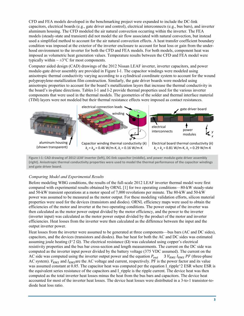
CFD and FEA models developed in the benchmarking project were expanded to include the DC-link capacitors, electrical boards (e.g., gate driver and control), electrical interconnects (e.g., bus bars), and inverter aluminum housing. The CFD modeled the air natural convection occurring within the inverter. The FEA models (steady-state and transient) did not model the air flow associated with natural convection, but instead used a simplified method to account for the air natural convection effects. A heat transfer coefficient boundary condition was imposed at the exterior of the inverter enclosure to account for heat loss or gain from the under-hood environment to the inverter for both the CFD and FEA models. For both models, component heat was imposed as volumetric heat generation values. Temperature results between the CFD and FEA model were typically within ~ ±3°C for most components. Computer aided design (CAD) drawings of the 2012 Nissan LEAF inverter, inverter capacitors, and power module-gate driver assembly are provided in Figure I-1. The capacitor windings were modeled using anisotropic thermal conductivity varying according to a cylindrical coordinate system to account for the wound polypropylene-metallization film construction. Similarly, the gate driver boards were modeled using anisotropic properties to account for the board’s metallization layers that increase the thermal conductivity in the board’s in-plane directions. Tables I-1 and I-2 provide thermal properties used for the various inverter components that were used in the thermal models. The geometries of the solder and thermal interface material (TIM) layers were not modeled but their thermal resistance effects were imposed as contact resistances.
Figure I-1: CAD drawing of 2012 LEAF inverter (left), DC-link capacitor (middle), and power module-gate driver assembly (right). Anisotropic thermal conductivity properties were used to model the thermal performance of the capacitor windings and gate driver board.
Comparing Model and Experimental Results Before modeling WBG conditions, the results of the full-scale 2012 LEAF inverter thermal model were first compared with experimental results obtained by ORNL [1] for two operating conditions—80-kW steady-state and 50-kW transient operations at a motor speed of 7,000 revolutions per minute. The 80-kW and 50-kW power was assumed to be measured as the motor output. For these modeling validation efforts, silicon material properties were used for the devices (transistors and diodes). ORNL efficiency maps were used to obtain the efficiencies of the motor and inverter at the two operating conditions. The power output of the inverter was then calculated as the motor power output divided by the motor efficiency, and the power to the inverter (inverter input) was calculated as the motor power output divided by the product of the motor and inverter efficiencies. Heat losses from the inverter were then calculated as the difference between the input and the output inverter power. Heat losses from the inverter were assumed to be generated at three components—bus bars (AC and DC sides), capacitors, and the devices (transistors and diodes). Bus bar heat for both the AC and DC sides was estimated assuming joule heating (I^2 Ω). The electrical resistance (Ω) was calculated using copper’s electrical resistivity properties and the bus bar cross-section and length measurements. The current on the DC side was computed as the inverter input power divided by the battery voltage (375 VDC assumed). The current on the AC side was computed using the inverter output power and the equation 𝑃𝑃𝑜𝑜𝑜𝑜𝑜𝑜 = 3 𝑉𝑉𝑅𝑅𝑅𝑅𝑅𝑅 𝐼𝐼𝑅𝑅𝑅𝑅𝑅𝑅 𝑃𝑃𝑃𝑃 (three-phase AC system). 𝑉𝑉𝑅𝑅𝑅𝑅𝑅𝑅 and 𝐼𝐼𝑅𝑅𝑅𝑅𝑅𝑅are the AC voltage and current, respectively. PF is the power factor and its value was assumed constant at 0.85. The capacitor heat was computed per the equation I_ripple^2 ESR where ESR is the equivalent series resistance of the capacitors and I_ripple is the ripple current. The device heat was then computed as the total inverter heat losses minus the heat from the bus bars and capacitors. The device heat accounted for most of the inverter heat losses. The device heat losses were distributed in a 3-to-1 transistor-to-diode heat loss ratio.
Electrical board thermal conductivity (k)kx = ky = 0.81 W/m-K, kz = 0.29 W/m-K
z
xypower
modulesz
rφ
Capacitor winding thermal conductivity (k)kz = kφ = 0.46 W/m-K, kr = 0.16 W/m-K
winding
electrical connection leads gate driver board
electrical interconnects
aluminum housing (shown transparent)

4
Table I-1: Material properties for the inverter power module components. Materials that do not have a reference source were assumed values.
SiC [3]
Die Solder Substrate Solder
Copper-Moly (20-80) [4]
Copper [3]
Module Plastic [5]
Silicone [6]
Dielectric pad
TIM
Thermal Conductivity (W/m-K)
270
Contact resistance: R"th = 2 mm^2-K/W
Contact resistance: R"th = 1 mm^2-K/W
160 387 0.34 0.26
Contact resistance: R"th = 116 mm^2-K/W
Contact resistance: R"th = 55 mm^2-K/W
Density (kg/m3) 3,160 9,850 8,933 1,800 1,272
Specific Heat (J/kg-K) 675 270 385 1,250 1,800
Table I-2: Material properties for the other inverter components. Materials that do not have a reference source were assumed values.
Capacitor Encapsulant
Capacitor Windings
Copper Leads (Bus Bars) [3]
Housing Aluminum [9]
Electrical Boards [10]
Bus Bar Molding Plastic
Thermal Conductivity (W/m-K)
0.45 [7] radial=0.16; angular, axial=0.46
387 167 in plane: 0.81: through plane: 0.29
0.34
Density (kg/m3) 1,200 [8] 900 8,933 2,00 1,900 1,800
Specific Heat (J/kg-K) 900 [8] 1,690 385 896 1,150 1,500
The results from the model comparison with ORNL results are provided in Figure I-2. A temperature probe was placed within the capacitor models at a location that corresponded to the location of a thermistor that was embedded within the capacitor’s encapsulating epoxy. This allowed for a direct comparison between experimental and model temperature results. The left plot in Figure I-2 shows the CFD-predicted maximum insulated-gate bipolar transistor, capacitor, and gate driver board temperatures for the 80-kW steady-state condition. As shown, the model-predicted results of 75.2°C compared well with the measured temperature of 75°C. The right plot in Figure I-2 plots experimental and transient FEA-predicted capacitor temperature versus time response for the 50 kW operating condition. The transient FEA model results were found to provide a reasonable match with experimental results. Only the capacitor temperatures were compared because this was the only inverter temperature measurement provided in ORNL’s tests. As previously mentioned, the junction-to-coolant model results have been previously validated in an NREL report [2].
Modeling High-Temperature WBG Devices within an Automotive Inverter The LEAF inverter thermal models were used to simulate high-temperature WBG devices within an automotive inverter. The effect of increasing the transistor (metal–oxide–semiconductor field-effect transistor [MOSFET]) temperatures to 175°C, 200°C, and 250°C on inverter component temperatures was computed via modeling. Of particular interest were the maximum temperatures of the capacitors, gate driver, and power module attach layers (i.e., solder) under elevated WBG-temperature conditions. SiC material properties imposed for the devices were used to simulate the WBG devices within the 2012 LEAF inverter. Maximum MOSFET temperatures of 175°C, 200°C, and 250°C were achieved by increasing the MOSFET heat (per device) to 223 W (99 W/cm^2), 273 W (121 W/cm^2), and 375 W (167 W/cm^2), respectively. Maintaining the 3-to-1, MOSFET-to-diode heat loss ratio resulted in total power module (three modules) heat dissipation of 5,350 W, 6,560 W, and 9,010 W for the 175°C, 200°C, and 250°C maximum junction temperature cases, respectively. Increasing the power module heat dissipation means that the inverter power also increases, assuming the inverter efficiency does not change. This increase in inverter power would require

5
a redesign of the inverter including increasing the bus bars sizes and changing the number of capacitors to account for the higher current levels. Since the current model does not change the inverter geometry, three capacitors and bus bars heat dissipation cases were evaluated for the elevated device temperature conditions (Table I-3). In Case 1, the bus bars and capacitors did not generate heat. In Case 2, the bus bar and capacitor heat generation rates were computed for an 80 kW and 97% efficiency (pertaining to a maximum junction temperature of 125°C) condition and those values were used for all elevated junction temperatures evaluated. For Case 2, the assumption is that the bus bar size and number of capacitors would increase to accommodate the increased power, but the heat dissipated per component would remain the same. For Case 3, the bus bar and capacitor heat was taken as a percentage of the power module heat and that percentage was used to compute their heat generation rates at the elevated junction temperature conditions. The percentages of heat for the components were taken at the 80 kW 97% efficiency condition. Case 3 represents the most extreme heat dissipation condition.
Figure I-2: CFD-computed temperatures for the steady-state 80 kW operating condition (left) and transient FEA-generated capacitor temperature response for the 50 kW operating condition (right). Both the steady-state and transient model results compared well with experimentally obtained data from ORNL [1].
Table I-3: Capacitor and bus bar (AC and DC sides) total heat dissipated for each case.
Case Capacitors (Total) Bus Bars (Total)
1 0 0
2 1.6 W 21.2 W
3 0.06% of module heat 0.72% of module heat
In addition to evaluating the effect of high-temperature WBG devices, the thermal models also evaluated three under-hood environment temperature conditions: 75°C, 125°C, and 140°C. The 75°C environment represents the under-hood conditions of an all-electric vehicle while the 125°C and 140°C environments represent under-hood conditions for hybrid electric vehicles. The hotter temperatures for the hybrid electric vehicles are associated with the heat generated by the internal-combustion engine. The more extreme under-hood case of 140°C represents a situation where the inverter is placed in close proximity to the combustion engine. The effect of the under-hood temperatures were imposed as heat transfer coefficient boundary conditions applied to the exterior of the inverter housing. A heat transfer coefficient of 10 W/m^2/K was used to simulate natural convection. Figure I-3 (left) provides the CFD-computed maximum capacitor temperatures for the 175°C, 200°C, and 250°C junction temperature cases at the three under-hood temperature environments (75°C, 125°C, and 140°C values shown in the figure legend). The maximum capacitor temperature was the maximum temperature found on any of the nine capacitor winding structures (see Figure I-1). Results are provided for the three cases listed in Table I-3. The values provided are the capacitor temperatures for Case 2. The error bar’s lower and upper limits denote the temperatures for Cases 1 and 3, respectively. Results show that even for the lowest junction temperature case of 175°C, the capacitors are predicted to exceed the 85°C temperature limit (typical limit for
85.2
75.2
78.3
70
80
90
100
IGBT Capacitor (thermistorlocation)
Gate driver
Max
imum
Tem
pera
ture
(°C
)
CFD
0
10
20
30
40
50
60
70
0 10 20 30 40 50 60
Tem
pera
ture
(°C
)
Time (minutes)
ORNL experimental data
Model (capacitor thermistor location)
ORNL-thermistor-measured capacitor temperature = ~75°C

6
polypropylene-film capacitors). For the 250°C junction temperature condition, capacitor temperatures approach 140°C. Several DOE projects are working to develop capacitors capable of operating at temperatures up to 140°C [11-13]. According to our analyses, the 140°C capacitor temperature rating is an appropriate target for high-temperature WBG conditions. Increasing under-hood temperature from 75°C to 140°C results in a maximum capacitor temperature increase of about 7°C and thus the under-hood environment is not predicted to have a significant effect on capacitors temperatures. The aluminum housing with integrated cold plate is believed to create a somewhat sheltered temperature environment within the inverter as the heat on the invert housing is conducted through the housing walls to the cold plate and ultimately dissipated to the coolant. Figure I-3 (right) shows the DC-side bus bar and capacitor winding temperature contours for the 175°C junction temperature case (75°C under-hood). These results show that the excessive capacitor temperatures are associated with heat from the power modules that is being conducted through the bus bars to the capacitors. Therefore, cooling the bus bars is a strategy to decrease capacitor temperatures.
Figure I-3: CFD-computed maximum capacitor winding temperatures for MOSFET temperatures of 175°C, 200°C, and 250°C (left). The under-hood temperatures are provided in the plot legend. CFD-computed DC bus bar and capacitor winding temperatures (right). Results demonstrate that heat is conducted from the power modules to the capacitors via the bus bars.
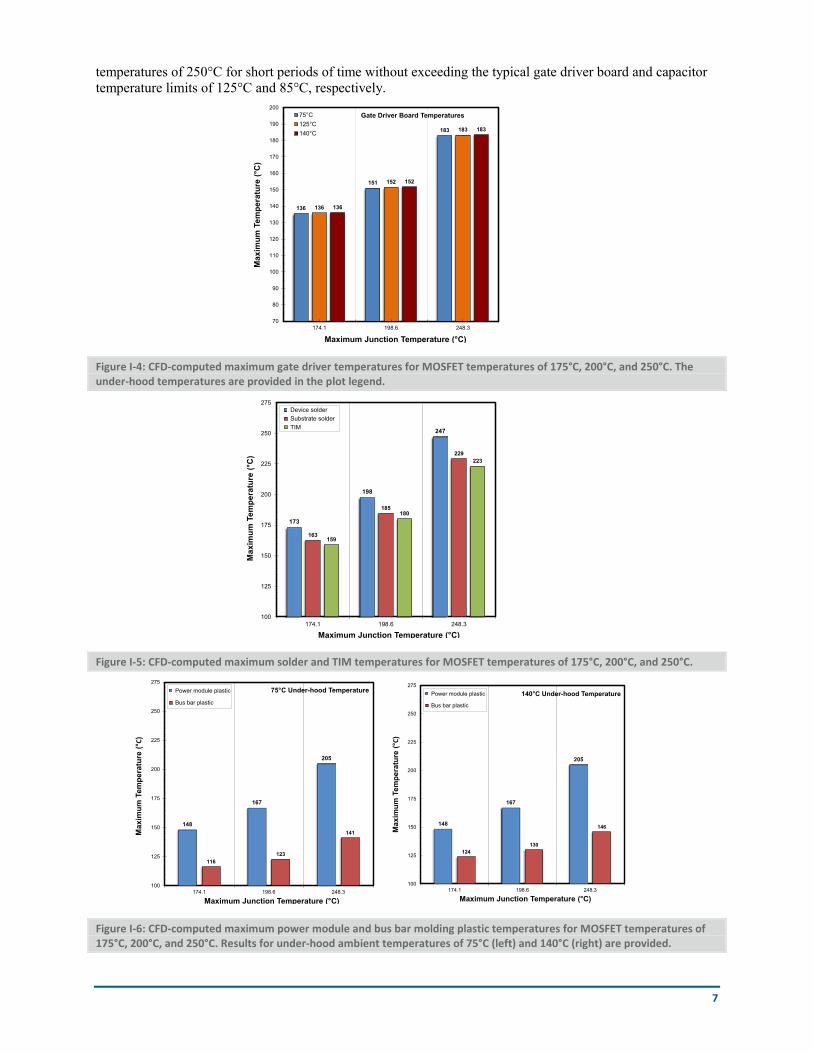
Figure I-4 provides the CFD-computed maximum gate driver temperatures for the 175°C, 200°C, and 250°C junction temperature cases at the three under-hood temperature environments (75°C, 125°C, and 140°C values shown in the figure legend). The different operating conditions described as Cases 1–3 and shown in Table I-3 had no effect on gate driver temperatures. Therefore, only one gate driver temperature value is provided for each condition. As shown, varying the under-hood temperature has a negligible on the gate driver temperatures. This effect is associated with the proximity of the gate driver boards to the power modules, which makes them more sensitive to device temperatures and less sensitive to under-hood temperatures. Results show that even for the lowest junction temperature case of 175°C, the gate drivers are predicted to exceed the 125°C temperature limit (typical limit for electrical boards). At 250°C junction temperatures, the gate driver is predicted to reach a temperature of 183°C.These results indicate that either high-temperature gate drivers are required or thermal management solutions are needed to enable gate drivers to operate under high-temperature WBG conditions. Figure I-5 provides the estimated solder and TIM temperatures for the three junction cases. The device solder temperatures are essentially equal to the device temperatures. Results indicate that high-temperature solders are required for WBG temperatures. Additionally, high-temperature TIMs may also be required. TIM temperatures reach 223°C for the 250°C junction temperature case which is well above the limit for most TIMs. Figure I-6 provides the power module and bus bar molding plastic maximum temperatures for the three junction temperature cases and for two under-hood temperature conditions (75°C and 140°C). Transient FEA simulations were conducted to estimate the time that it takes for the capacitors and gate drivers to reach thermal equilibrium for the 250°C junction temperature condition (9,010 W power module heat in a 3-to-1 MOSFET-to-diode heat loss ratio and bus bar and capacitor temperatures defined as Case 2 and provided in Table I-3). An initial temperature of 50°C was imposed for all inverter components. Figure I-7 shows the temperature versus time response for the MOSFETs, gate driver board, and capacitors. As shown, the MOSFETs achieve temperature equilibrium within a few seconds while the gate driver and capacitors require several minutes to reach steady-state conditions. The results indicate that it is possible to operate at junction
108
115
130
113
120
135
114
122
137
70
80
90
100
110
120
130
140
150
174.1 198.6 248.3
Max
imum
Tem
pera
ture
(°C
)
Maximum Junction Temperature (°C)
Capacitor Temperatures75°C
125°C
140°C
7
temperatures of 250°C for short periods of time without exceeding the typical gate driver board and capacitor temperature limits of 125°C and 85°C, respectively.
Figure I-4: CFD-computed maximum gate driver temperatures for MOSFET temperatures of 175°C, 200°C, and 250°C. The under-hood temperatures are provided in the plot legend.
Figure I-5: CFD-computed maximum solder and TIM temperatures for MOSFET temperatures of 175°C, 200°C, and 250°C.
Figure I-6: CFD-computed maximum power module and bus bar molding plastic temperatures for MOSFET temperatures of 175°C, 200°C, and 250°C. Results for under-hood ambient temperatures of 75°C (left) and 140°C (right) are provided.
136
151
183
136
152
183
136
152
183
70
80
90
100
110
120
130
140
150
160
170
180
190
200
174.1 198.6 248.3
Max
imum
Tem
pera
ture
(°C
)
Maximum Junction Temperature (°C)
Gate Driver Board Temperatures75°C125°C140°C
173
198
247
163
185
229
159
180
223
100
125
150
175
200
225
250
275
174.1 198.6 248.3
Max
imum
Tem
pera
ture
(°C
)
Maximum Junction Temperature (°C)
Device solder Substrate solder TIM
148
167
205
124130
146
100
125
150
175
200
225
250
275
174.1 198.6 248.3
Max
imum
Tem
pera
ture
(°C)
Maximum Junction Temperature (°C)
140°C Under-hood Temperature Power module plastic
Bus bar plastic
148
167
205
116123
141
100
125
150
175
200
225
250
275
174.1 198.6 248.3
Max
imum
Tem
pera
ture
(°C)
Maximum Junction Temperature (°C)
75°C Under-hood Temperature Power module plastic
Bus bar plastic

8
Figure I-7: Transient FEA-estimated temperature response for the MOSFETs, gate driver board, and capacitors.
Evaluating Capacitor Cooling Strategies A modified version of the LEAF inverter was used to evaluate the various capacitor cooling strategies. The modifications included placing the capacitors below the power modules as is shown in Figure I-8. This configuration allows for the placement of a cold plate between the power modules, capacitors, and bus bars. This cold plate configuration enables cooling of the capacitors and bus bars in addition to the power modules. The modified model only included the capacitors, DC-side bus bars, and power modules because prior analysis indicated that capacitor excess temperatures were mostly associated with heat conduction through the bus bars. FEA was conducted to evaluate three capacitor cooling strategies: 1) improved cooling on the power modules to decrease junction temperatures, 2) directly cooling the capacitors using cold plates, and 3) cooling the DC-side bus bars using cold plates. The FEA only modeled one power module and one capacitor winding embedded within an epoxy encapsulant. Two bus bar configurations were evaluated (Figure I-9). For bus bar Configuration A, the bus bars are placed side-by-side in a configuration that is typically used in inverters. For bus bar Configuration B, the bus bars are separate. Modeling the two configurations allows the effect of the bus bar design on the capacitor cooling strategies to be evaluated. Only the heat dissipated by the power modules was imposed in the models because capacitor temperatures are mostly dictated by the power module heat and not self-heating of the capacitors. Power module heat was imposed in a 3-to-1, MOSFET-to-diode heat loss ratio. The effect of power module cooling performance on maximum capacitor temperatures is shown in Figure I-10. A total of 1,784 W was dissipated by the devices, which produced a 175°C junction temperature for the baseline convective resistance case of 133 mm^2-K/W (convective resistance estimated for the LEAF cold plate at 10 liters per minute). As shown, reducing the convective resistance to 20 mm^2-K/W (85% reduction with respect to the baseline) reduces the junction temperature by 20°C and the capacitor temperature by 17°C. Therefore, improving the power module cold plate performance results in lower capacitor temperatures but the capacitor temperatures are still predicted to exceed 85°C for all cases evaluated. As expected, bus bar configuration has no effect on capacitor temperatures for this cooling strategy.
Figure I-8: CAD drawing of the modified LEAF inverter used to evaluate various capacitor cooling strategies. This modified configuration would enable placing a cold plate between all components to aid in cooling the capacitors (right).
0
50
100
150
200
250
300
0 20 40 60 80 100 120
Max
imum
Tem
pera
ture
(°C
)
Time (minutes)
MOSFETs
Gate driver board
Capacitor windings
Cold plate

9
Figure I-9: Bus bar Configurations A (top) and B (bottom). FEA was conducted to evaluate three capacitor cooling strategies: 1) increased cooling on the power module cold plate, 2) using cold plates on one or both sides of the capacitor, and 3) using cold plates on one or both sides of the DC bus bars.
The effects of using cold plates to cool the capacitors are shown in shown in Figure I-11. Results are provided for the 175°C, 200°C, and 250°C junction temperature cases. A 3.25-mm-thick aluminum cold plate with a TIM thermal resistance of 55 mm^2-K/W at the cold plate-capacitor interface was used. Three capacitor cold plate strategies were evaluated: 1) cooling the capacitor’s top surface (side 1 in Figure I-9), 2) cooling the capacitor’s lower-surface (side 2 in Figure I-9), and 3) cooling both sides of the capacitor. Cooling one side of the capacitor provides slightly different capacitor temperatures for the two bus bar configurations—different thermal resistance through the bus bars for the two configurations is believed to be the reason for this effect. Additionally, cooling only one side of the capacitors does not enable capacitor temperatures <85°C. The capacitor electrical leads (hottest components) enter the capacitor encapsulant through the top and therefore cooling the top surface (side 1) is more effective as compared to cooling the lower surface. According to the analysis, a double-side cold plate cooling strategy would enable the capacitors to operate at temperatures below 85°C for junction temperatures up to 200°C. The double-side cold plate cooling solution does not provide sufficient capacitor cooling for the 250°C junction temperature case.
Figure I-10: Maximum capacitor temperatures versus the power module cold plate convective resistance. Reducing the power module convective resistance from 133 mm^2-K/W to 20 mm2-K/W reduces the capacitor maximum temperature by ~17°C.
1
3
2side 1
side 2
side 1 side 2
18 mm
cooled length: 30 mm
75.4 mm
21.6 mm
1-mm-thick plastic between bus bars
2-mm-thick copper bus bars
1
3
2side 1
side 2
side 1
18 mm
67.5 mm
20 mm
2-mm-thick copper bus bars
cooled length: 30 mm
Bus bar configuration A
Bus bar configuration B
70
80
90
100
110
120
130
140
150
0 50 100 150 200
Max
imum
cap
acito
r tem
pera
ture
(°C
)
Convective thermal resistance (mm2-K/W)
Power module total heat: 1,784 W
Configuration A Configuration B
Tj=175°C
Tj=161°C
Tj=155°C

10
Figure I-11: Maximum capacitor temperatures plotted versus the capacitor cold plate convective thermal resistance. The 175°C, 200°C, and 250°C junction temperature case results are provided. Results show that using two cold plates on the capacitor can enable the capacitor to operate below 85°C for junction temperatures up to 200°C.
The effects of using cold plates to cool the DC-side bus bars are shown in shown in Figure I-12. Results are provided for the 175°C, 200°C, and 250°C junction temperature cases. Three bus bar cold plate strategies were evaluated for Configuration A—cooling the bus bar’s front surface (side 1 in Figure I-9), cooling the bus bar’s back-surface (side 2 in Figure I-9), and cooling both sides of the bus bars. Bus bar sides 1 and 2 are identical in surface area. The main difference between the two sides is that each side is connected to a different power module terminal (positive or negative). Due to the electrical lead layout with the power module, the different power module terminals operate at slightly different temperatures. Two bus bar cold plate strategies were evaluated for Configuration B—cooling the bus bar’s front surface (side 1 in Figure I-9) and cooling both sides of the bus bars. Only one side was cooled for Configuration B because its symmetric bus bar design meant that cooling the front side (side 1) was equivalent to cooling the back side. A heat transfer coefficient boundary condition was applied to the bus bar copper surface(s) to simulate cold plate cooling. Thermal resistances of magnitudes 181 mm^2-K/W and 19.5 mm^2-K/W were subtracted from the imposed convective resistance (inverse of the heat transfer coefficient) to account for the resistances associated with a dielectric pad and a 3.25-mm-thick aluminum cold plate. Therefore, the convective resistance values provided in Figure I-12 are the resistances associated with the coolant and any area enhancement features (e.g., fins). The results indicated that cooling the bus bars is an effective means to cool the capacitors. Cooling one or both sides of the bus bars enables the capacitor to operate at temperatures below 85°C even at the highest junction temperature of 250°C. Moreover, the bus bar cold plate convective thermal resistance values required to achieve capacitor temperatures below 85°C can be relatively high (~1,000 mm^2-K/W equivalent to an overall heat transfer coefficient of 1,000 W/m^2-K). Bus bar cooling for Configuration A initially provides lower capacitor temperature due to its larger cooled surface area as compared with Configuration B.
Figure I-12: Maximum capacitor temperatures plotted versus the bus bar cold plate convective thermal resistance. The 175°C, 200°C, and 250°C junction temperature case results are provided. Results indicated that mounting cold plates to the bus bars enables capacitor temperature to operate below 85°C at all junction temperatures evaluated.
Figure I-13 shows the effect of increasing the bus bar cooled surface area on capacitor temperatures. The cooled surface area was increased by increasing the cooled length dimension shown in Figure I-9. Cooled
70
80
90
100
110
120
130
140
150
10 100 1,000 10,000 100,000
Max
imum
cap
acito
r tem
pera
ture
(°C
)
Convective thermal resistance (mm2-K/W)
Tj, maximum = 175°C
Configuration A (side 1) Configuration A (side 2) Configuration A (double side) Configuration B (side 1) Configuration B (side 2) Configuration B (double side)
70
80
90
100
110
120
130
140
150
10 100 1,000 10,000 100,000
Max
imum
cap
acito
r tem
pera
ture
(°C
)
Convective thermal resistance (mm2-K/W)
Tj, maximum = 200°C
Configuration A (side 1) Configuration A (side 2) Configuration A (double side) Configuration B (side 1) Configuration B (side 2) Configuration B (double side)
70
80
90
100
110
120
130
140
150
10 100 1,000 10,000 100,000
Max
imum
cap
acito
r tem
pera
ture
(°C
)
Convective thermal resistance (mm2-K/W)
Tj, maximum = 250°C
Configuration A (side 1) Configuration A (side 2) Configuration A (double side) Configuration B (side 1) Configuration B (side 2) Configuration B (double side)
50
70
90
110
130
150
170
10 100 1,000 10,000 100,000
Max
imum
cap
acito
r tem
pera
ture
(°C
)
Convective thermal resistance (mm2-K/W)
Tj, maximum = 175°C
Configuration A (side 1) Configuration A (side 2) Configuration A (double side) Configuration B (side 1) Configuration B (double side)
50
70
90
110
130
150
170
10 100 1,000 10,000 100,000
Max
imum
cap
acito
r tem
pera
ture
(°C
)
Convective thermal resistance (mm2-K/W)
Tj, maximum = 200°C
Configuration A (side 1) Configuration A (side 2) Configuration A (double side) Configuration B (side 1) Configuration B (double side)
50
70
90
110
130
150
170
10 100 1,000 10,000 100,000
Max
imum
cap
acito
r tem
pera
ture
(°C
)
Convective thermal resistance (mm2-K/W)
Tj, maximum = 250°C
Configuration A (side 1) Configuration A (side 2) Configuration A (double side) Configuration B (side 1) Configuration B (double side)

11
lengths of 30 mm, 60 mm, and 90 mm were evaluated. The cooled surface areas for each configuration are provided in the figure legends. Results show that increasing the cooled surface area is more beneficial for higher convective resistance values (>1,000 mm^2-K/W).
Figure I-13: Maximum capacitor temperatures plotted versus the bus bar cold plate convective thermal resistance for the 250°C junction temperature case. The effect of increasing the bus bar cooled surface area (increasing the bus bar cooled length to 30 mm, 60 mm, and 90 mm, see Figure I-9) on capacitor temperatures was evaluated. Cooling was only applied to one side of the bus bars. The figure legend provides the total cooled area.
Conclusions and Future Directions
Conclusions ● Modeling analyses indicate that capacitors and gate drivers are expected to exceed their typical
temperature operating limits when exposed to high WBG temperatures (175°C, 200°C, and 250°C). The electrical interconnections (e.g., bus bars) are the primary thermal paths through which heat from the devices is conducted to the other components.
● Under-hood temperature environments are not predicted to have a significant effect on inverter component temperatures. The aluminum inverter enclosure provides a sheltered environment that limits the effect of under-hood temperature changes.
● Transient thermal simulations of an automotive inverter revealed that it may be possible to operate at 250°C junction temperatures, for short periods of time (several minutes), without exceeding the capacitor and gate driver typical temperature limits of 85°C and 125°C, respectively.
● Three capacitor cooling strategies were evaluated: 1) improving power module cold plate performance, 2) using cold plates on the capacitors, and 3) using cold plates on the bus bars. Using cold plates to cool the bus bars was the most effective strategy for cooling the capacitors. This cooling approach enables capacitor operating temperatures below 85°C at junction temperatures of 250°C. Moreover, a relatively low thermal performance cold plate placed on the bus bars can enable safe capacitor operation at high-temperature WBG conditions.
Future Directions ● Evaluate effect of module design on the various capacitor cooling strategies.
● Evaluate gate driver cooling strategies.
● Conduct experimental validation of key thermal concepts identified in the modeling work.
● Evaluate motor-related inverter heating effects.
50
70
90
110
130
150
170
10 100 1,000 10,000 100,000
Max
imum
cap
acito
r tem
pera
ture
(°C
)
Convective thermal resistance (mm2-K/W)
Tj, maximum = 250°C, Configuration A
2,262 mm^2 4,524 mm^2 6,786 mm^2
50
70
90
110
130
150
170
10 100 1,000 10,000 100,000
Max
imum
cap
acito
r tem
pera
ture
(°C
)
Convective thermal resistance (mm2-K/W)
Tj, maximum = 250°C, Configuration B
1,080 mm^2 2,160 mm^2 3,240 mm^2

12
Nomenclature
I electrical current
k thermal conductivity
R"th specific thermal resistance
T temperature
Ω electrical resistance
Subscripts
j junction
RMS root mean squared
r, z, φ cylindrical system coordinates (radial, axial, and angular)
x, y, z Cartesian system coordinates
FY 2016 Presentations/Publications/Patents
1. Bennion, K. “Power Electronics Thermal Management Research.” 2016 DOE VTO Annual Merit Review, Washington, DC, June 2016.
2. Moreno, G. “Power Electronics Thermal Management Research.” 2016 presentation to the DOE VTO Electrical and Electronics Technical Team, Southfield, MI, July 2016.
Acknowledgments
The author would like to acknowledge the support provided by Susan Rogers, Technology Development Manager for the Electric Drive Technologies Program, Vehicle Technologies Office, U.S. Department of Energy Office of Energy Efficiency and Renewable Energy. The significant contributions of Kevin Albrecht, Kevin Bennion, and Xuhui Feng are acknowledged.
References
[1] Burress, T. “Benchmarking of Competitive Technologies.” 2012 DOE VTO Annual Report, http://energy.gov/sites/prod/files/2014/03/f8/2012_apeem_report.pdf [Accessed: 2-Mar-2016]. [2] Moreno, G. “Thermal Performance Benchmarking” 2015 DOE VTO Annual Report, http://energy.gov/sites/prod/files/2016/03/f30/FY%202015%20Electric%20Drive%20Technologies%20Annual%20Report.pdf [Accessed: 2-Sept-2016]. [3] Lau, J.H., and Pao, Y.H.. “Solder joint reliability of BGA, CSP, flip chip, and fine pitch SMT assemblies," 1997, NY McGraw-Hill. [4] Spectra-Mat, Inc. “Molybdenum-Copper Components” [Online]. Available: http://www.spectramat.com/pdf/PB-600-D%20Molybdenum%20Copper%20Components.pdf [Accessed: 18-Mar-2016]. [5] MatWeb Material Property Data. “Overview of Materials for Polyphenylene Sulfide (PPS)” [Online]. Available: http://www.matweb.com/search/datasheet.aspx?matguid=301e3f904d6a43a7922601c9d11ded91 [Accessed: 18-Mar-2016]. [6] MatWeb Material Property Data. “Overview of materials for Silicone, RTV, Encapsulation Grade” [Online]. Available: http://www.matweb.com/search/DataSheet.aspx?MatGUID=5660dbe1b55f4826809455e890cac682 [Accessed: 18-Mar-2016].

13
[7] LORD Electronic Materials. “Circalok™ 6028/6029 Epoxy Encapsulant” [Online]. Available http://www.lord.com/products-and-solutions/electronic-materials/circalok-60286029-epoxy-encapsulant [Accessed: 20-Mar-2016]. [8] MG Chemicals. “Thermally Conductive Epoxy Encapsulating & Potting Compound 832TC Technical Data Sheet” [Online]. Available: http://www.mgchemicals.com/downloads/tds/tds-832tc-2parts.pdf [Accessed: 20-Mar-2016]. [9] MatWeb Material Property Data. “Aluminum 6061-T6; 6061-T651” [Online]. Available: http://www.matweb.com/search/datasheet.aspx?matguid=1b8c06d0ca7c456694c7777d9e10be5b [Accessed: 18-Mar-2016]. [10] Azar, K., and Graebner, J.E.. "Experimental determination of thermal conductivity of printed wiring boards." Semiconductor Thermal Measurement and Management Symposium, 1996. SEMI-THERM XII Proceedings. IEEE, 1996. [11] Balachandran, U. “Cost-Effective Fabrication of High-Temperature Ceramic Capacitors for Power Inverters.” 2014 DOE VTO Annual Report, http://energy.gov/sites/prod/files/2015/04/f21/FY14_EDT_Annual_Report.pdf [Accessed: 9-Sept-2016]. [12] Yializis, A. “High Temperature DC Bus Capacitor Cost Reduction & Performance Improvements.” 2014 DOE VTO Annual Report, http://energy.gov/sites/prod/files/2015/04/f21/FY14_EDT_Annual_Report.pdf [Accessed: 9-Sept-2016]. [13] Tan, D. “High Performance DC Bus Film Capacitor.” 2014 DOE VTO Annual Report, http://energy.gov/sites/prod/files/2015/04/f21/FY14_EDT_Annual_Report.pdf [Accessed: 9-Sept-2016].