Embed Size (px)
Citation preview
POWER MANAGEMENT
1 www.semtech.com
SC1176/SC1176ADual Synchronous Voltage Mode
Controller with Current Sharing Circuitry
Description Features
Applications
Revision: June 29, 2006
The SC1176 is a versatile 2 phase, synchronous, volt-age mode PWM controller that may be used in two dis-tinct ways. First, the SC1176 is ideal for applicationswhere point of use output power exceeds any single in-put power budget. Alternatively, the SC1176 can be usedas a dual switcher. The SC1176 features a temperaturecompensated voltage reference, over current protectionwith 50% fold-back and internal level-shifted, high-sidedrive circuitry.
In current sharing configuration, the SC1176 can pro-duce a single output voltage from two separate voltagesources (which can be different voltage levels) whilemaintaining current sharing between the channels. Cur-rent sharing is programmable to allow loading each inputsupply as required by the application.
In dual switcher configuration, two feedback paths areprovided for independent control of the separate out-puts. The device will provide a regulated output fromflexibly configured inputs (3.3V, 5V, 12V), provided 5V ispresent for VCC. The two switchers are 180° out of phaseto minimize input and output ripple.
The SC1176A has the phases of the Master and the Slaveinverted.
It offers a different pattern for ripple cancellation andprevents phase fold back during current limit.
The two chips are pin compatible.
300kHz fixed frequency operationSoft Start and Enable functionPower Good output providedOver current protection with 50% fold-backPhase-shifted switchers minimize rippleHigh efficiency operation, >90%Programmable output(s) as low as .9VIndustrial temperature rangeSOIC-20 or TSSOP-20 pin Lead free package. Thisproduct is fully WEEE and RoHS compliant
Two Phase, Current Sharing ControllerFlexible, same or separate VIN
Programmable current sharingCombined current limit with fold-back2 phases operating opposed for ripple reductionThermal distribution via multi-phase output
Two Independent PWM ControllersFlexible, same or separate VIN
Independent control for each channelIndependent and separate current limit2 phases operating opposed for ripple reduction (ifsame VIN used)
Graphics cardsDDR MemoryPeripheral add-in card
SSTL TerminationDual-Phase power supplyPower supplies requiring two outputs
2 2006 Semtech Corp. www.semtech.com
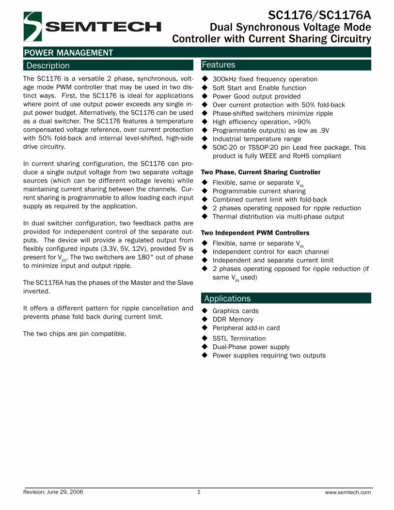
POWER MANAGEMENT
SC1176/SC1176A
Typical Application Circuit2 Channels with Current Sharing
3 2006 Semtech Corp. www.semtech.com
POWER MANAGEMENT
SC1176/SC1176A
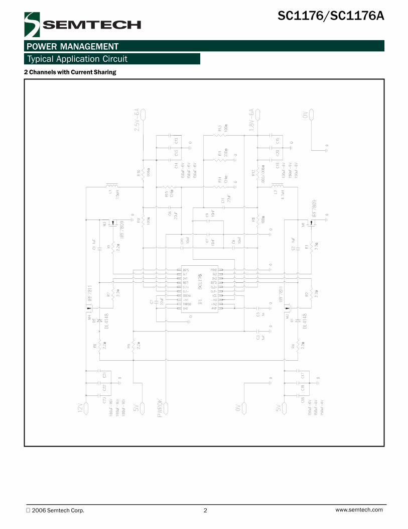
Electrical Characteristics
retemaraP snoitidnoC niM pyT xaM stinU
egatloVtuptuO IO A2= )1( V, TUO V57.2ottes 56.2 57.2 58.2 V
egatloVylppuS V CC 2.4 51 V
tnerruCylppuS V CC 0.5= 51 Am
egatloVecnerefeR I FER Aµ0= 98.0 9.0 19.0 V
noitalugeReniLegatloVecnerefeR V5 < V CC < V51 5.0 %
noitalugeRdaoLegatloVecnerefeR I FER Aµ03otAµ0= 21- Vm
noitalugeReniLtuptuO V5 < V NI < V51 5.0 %
noitalugeRdaoLtuptuO IO A51otA3.0= )1( 1 %
A(niaG LO ) V ESNESO Vot O 53 Bd
egatloVtimiLtnerruC 06 07 08 Vm
ycneuqerFrotallicsO 072 003 033 zHk
elcyCytuDxaMrotallicsO 09 59 %
tnerruCkniSHD V0.3=DNGP-HD 3.1 A
tnerruCkniSHD V0.2=DNGP-HD 58.0 A
tnerruCecruoSHD V5.3=HD-HTSB 3.1 A
tnerruCecruoSHD V5.2=HD-HTSB 58.0 A
Unless Specified: VCC = 4.75 to 5.25V, GND = PGND = 0V, FB = VO, 0mV < (CS(+) - (CS(-)) < 60mV , TJ = 25°C
retemaraP lobmyS stimiL stinU
V CC DNGot VIN 51ot3.0- V
DNGotDNGP 1± V
DNGotTSB 62ot3.0- V
esaCotnoitcnuJecnatsiseRlamrehTCIOS
POSSTθ CJ
4272
W/C°
tneibmAotnoitcnuJecnatsiseRlamrehTCIOS
POSSTθ AJ
5658
C° W/
gnitarepO egnaRerutarepmeTtneibmA TA 07ot0 C°
gnitarepO egnaRerutarepmeTnoitcnuJ TJ 521ot0 C°
egnaRerutarepmeTegarotS T GTS 051+ot56- C°
ces01)gniredloS(erutarepmeTdaeL T DAEL 003 C°
Absolute Maximum RatingExceeding the specifications below may result in permanent damage to the device, or device malfunction. Operation outside of the parameters specifiedin the Electrical Characteristics section is not implied.
4 2006 Semtech Corp. www.semtech.com
POWER MANAGEMENT
SC1176/SC1176A
Electrical Characteristics (Cont.)
RETEMARAP SNOITIDNOC NIM PYT XAM STINU
tnerruCkniSLD V0.3=GNGP-LD 3.1 A
tnerruCkniSLD V0.2=DNGP-LD 58.0 A
tnerruCecruoSLD V5.3=LD-LTSB 3.1 A
tnerruCecruoSLD V5.2=LD-LTSB 58.0 A
emiTdaeD 5etoN 05 001 051 sn
tnerruCegrahCtratStfoS )2( 52 Aµ
elbanEtratStfoS elcycytud%0 4.1 V
dnEtratStfoS elcycytud%001 5.2 V
noitisnarTtratStfoS )2( edomsuonorhcnyS 3.3 V
wodniWdooGrewoP )3( + 01 V% TUO
tnerruCkcaBdloF V TUO V0= %05 I MIL
eenKegatloVkcaBdloF =I MILI 9.0 V TUO V
tnerruCsaiBtupnI 2NI-,2NI+,1NI- 1 Aµ
egakaeLHDotHTSB V5=HD-HTSB 01 Aµ
egakaeLDNGPotHD V5=DNGP-HD 01 Aµ
egakaeLLDotLTSB V5=LD-LTSB 01 Aµ
DNGPotLD V5=DNGP-LD 01 Aµ
Notes:(1) Specification refers to application circuit.(2) The soft start pin sources 25µA to an external capacitor. The converter operates in synchronous mode above the softstart transition threshold and in asynchronous mode below it.(3) Power good is an open collector pulled low when the output voltage is outside the ±10% window.(4) This device is ESD sensitive. Use of standard ESD handling precautions is required.(5) 200ns maximum at 75°.
Unless Specified: VCC = 4.75 to 5.25V, GND = PGND = 0V, FB = VO, 0mV < (CS(+) - (CS(-)) < 60mV , TJ = 25°C
6
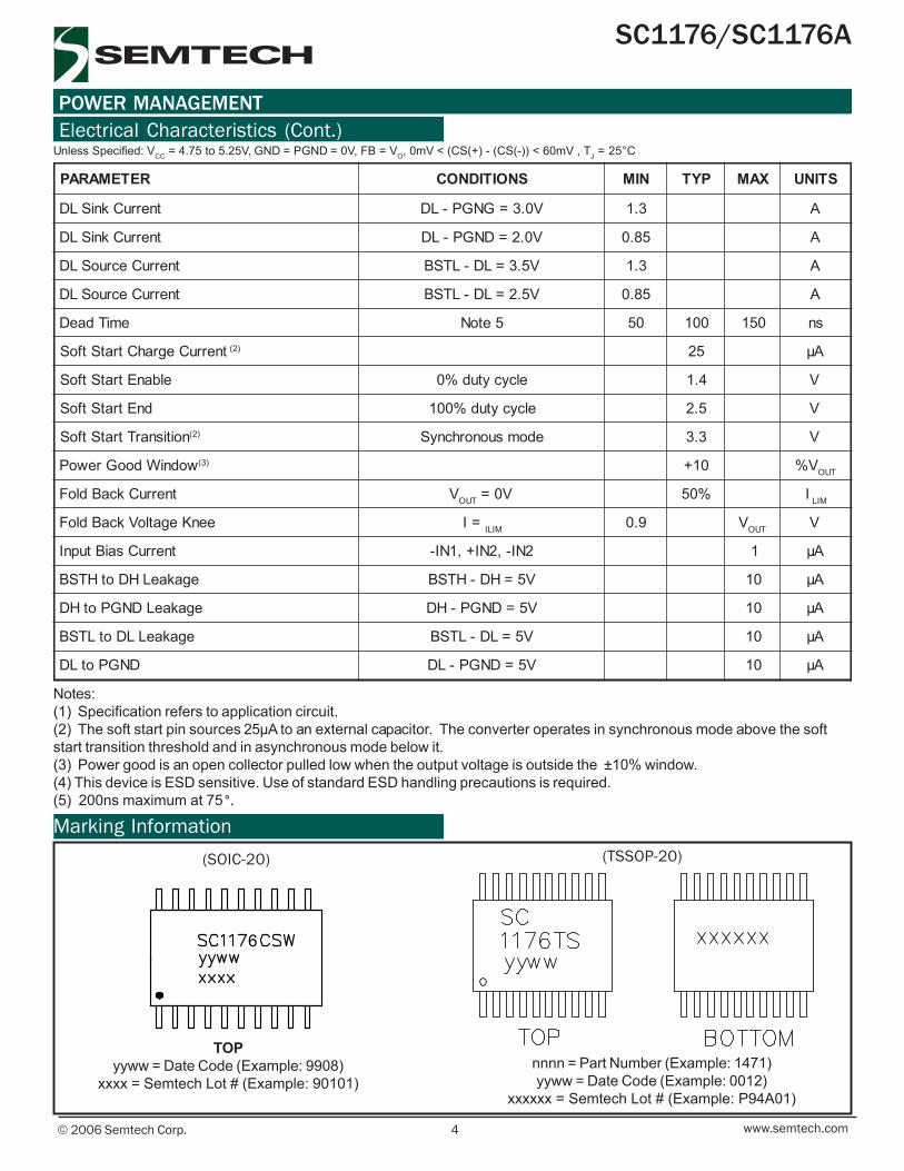
Marking Information
TOPyyww = Date Code (Example: 9908)
xxxx = Semtech Lot # (Example: 90101)
(SOIC-20) (TSSOP-20)
nnnn = Part Number (Example: 1471)yyww = Date Code (Example: 0012)
xxxxxx = Semtech Lot # (Example: P94A01)

5 2006 Semtech Corp. www.semtech.com
POWER MANAGEMENT
SC1176/SC1176A
Pin Configuration
EXPANDED PIN DESCRIPTION
Pin 1: (VREF)Internal .9V referenceConnected to the + input of the master channel erroramplifier.Pin 2: (+IN2)+ Input of slave channel error amplifier.Connected to .9V reference (Pin 1) for2 independent channel configuration.Pin 3, 18: (-IN2, -IN1)- Inputs of close loop error amplifiers.Works as a feedback inputs (For both modes).Pin 4: (VCC)VCC chip supply voltage.15V maximum, 15mA typical.Needs a 1µF ceramic multilayer decoupling capacitorto GND (Pin 20).Pin 5, 6,15, 16: (CL2-, CL2+, CL1+, CL1-)Pins (-) and (+) of the current limit amplifiers for bothchannels.Connected to output current sense resistors. Com-pares that sense voltage to internal 75mV reference.Needs RC filter for noise rejection.Pin 7, 14: (BST2, BST1)BST signal. Supply for high side driver.Can be connected to a high enough voltage source.Usually connected to bootstrap circuit.
Pin 8, 13: (DH2, DH1)DH signal (Drive High).Gate drive for top MOSFETs.Requires a small serie resistor.Pin 9, 12: (DL2, DL1)DL signal (Drive Low).Gate drive for bottom MOSFETs.Requires a small serie resistor.Pin 10: (PGND)Power GND. Return of gate drive currents.Pin 11: (BSTC)Supply for bottom MOSFETs gate drive.Pin 17: (SS/ENA)Soft start pin. Internal current source connected toexternal capacitor.Inhibits he chip if pulled down.Pin 19: (PWRGD)Power good signal.Open collector signal .Turns to 0 if output voltage is outside the power goodwindow.Pin 20: (GND)Analog GND.Return of analog signals and bias of chip.
eciveD )1( egakcaP )2(
RTWSC6711CS02-CIOS
TRTWSC6711CS
RTWSA6711CS
TRTWSA6711CS
RTST6711CS02-POSST
TRTST6711CS
RTSTA6711CS
1-BVE6711CS noitaulavEnoisreVerahStnerruCdraoB
2-BVE2-6711CS noitaulavEnoisreVlennahClauD
Notes:(1) Only available in tape and reel packaging. A reelcontains 1000 (SOIC) or 2500 (TSSOP) devices.
(2) Lead free product. This product is fully WEEE andRoHS compliant.
Pin Descriptions
Top View
(SOIC-20 and TSSOP-20 Pin)
Ordering Information
6 2006 Semtech Corp. www.semtech.com
POWER MANAGEMENT
SC1176/SC1176A
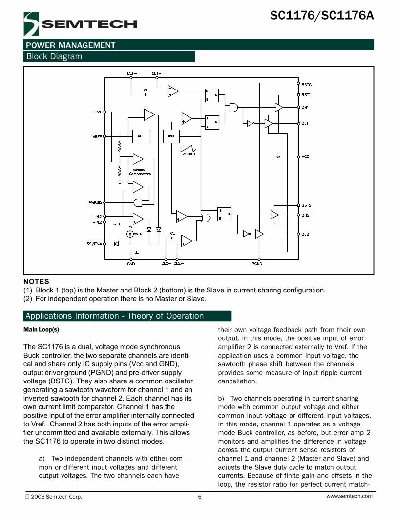
NOTES(1) Block 1 (top) is the Master and Block 2 (bottom) is the Slave in current sharing configuration.(2) For independent operation there is no Master or Slave.
Main Loop(s)
The SC1176 is a dual, voltage mode synchronousBuck controller, the two separate channels are identi-cal and share only IC supply pins (Vcc and GND),output driver ground (PGND) and pre-driver supplyvoltage (BSTC). They also share a common oscillatorgenerating a sawtooth waveform for channel 1 and aninverted sawtooth for channel 2. Each channel has itsown current limit comparator. Channel 1 has thepositive input of the error amplifier internally connectedto Vref. Channel 2 has both inputs of the error ampli-fier uncommitted and available externally. This allowsthe SC1176 to operate in two distinct modes.
a) Two independent channels with either com-mon or different input voltages and differentoutput voltages. The two channels each have
Block Diagram
Applications Information - Theory of Operationtheir own voltage feedback path from their ownoutput. In this mode, the positive input of erroramplifier 2 is connected externally to Vref. If theapplication uses a common input voltage, thesawtooth phase shift between the channelsprovides some measure of input ripple currentcancellation.
b) Two channels operating in current sharingmode with common output voltage and eithercommon input voltage or different input voltages.In this mode, channel 1 operates as a voltagemode Buck controller, as before, but error amp 2monitors and amplifies the difference in voltageacross the output current sense resistors ofchannel 1 and channel 2 (Master and Slave) andadjusts the Slave duty cycle to match outputcurrents. Because of finite gain and offsets in theloop, the resistor ratio for perfect current match-
7 2006 Semtech Corp. www.semtech.com
POWER MANAGEMENT
SC1176/SC1176A
ing is not 1:1. The Master and Slave channels stillhave their own current limits, identical to theindependent channel case.
Power GoodThe controller provides a power good signal. This is anopen collector output, which is pulled low if the outputvoltage is outside of the power good window.
Soft Start/EnableThe Soft Start/Enable (SS/ENA) pin serves several func-tions. If held below the Soft Start Enable threshold, bothchannels are inhibited. DH1 and DH2 will be low, turningoff the top FETs. Between the Soft Start Enable thresh-old and the Soft Start End threshold, the duty cycle isallowed to increase. At the Soft Start End threshold,maximum duty cycle is reached. In practical applicationsthe error amplifier will be controlling the duty cycle be-fore the Soft Start End threshold is reached. To avoidboost problems during startup in current share mode,both channels start up in asynchronous mode, and thebottom FET body diode is used for recirculating currentduring the FET off time. When the SS/ENA pin reachesthe Soft Start Transition threshold, the channels beginoperating in synchronous mode for improved efficiency.The soft start pin sources approximately 25uA and softstart timing can be set by selection of an appropriatesoft start capacitor value.
SENSE RESISTOR SELECTION
Current Sharing Mode
Calculation of the three programming resistors to achievesharing.Three resistors will determine the current sharing loadline.First the offset resistor will ensure that the load linecrosses the origin (0 Amp on each channel) for sharingat light current. A pull up resistor from the 5V bias (VCC ofthe chip) will be used. For low duty cycle on the slavechannel (below 50%), the pull up will be on pin 3. Forhigh duty cycle on the slave channel (above 50%), thepull up will be on pin 2.
Applications Information - Theory of Operation
The formula is:
SLAVE
OUT
OUTuppull
V1.V5.
V5X1.2)K(R+−
−=Ω−
100Ω being the value of the resistors connecting thepins 2 and 3 to the two output sense resistors.
.1 V is an estimated voltage drop across theMOSFETs.
Positive values go to pin 3, negative to pin 2.
A +20K will be a 20K on pin 3.A -20K will be a 20K on pin 2.
Now that the offset resistor has been fixed, we need toset up the maximum current for each channel.
Selection of RSENSE 1 for the master channel: (in mohm)
RSENSE 1 = 72mV / I max master
Selection of RSENSE 2 for the slave channel: (in m ohm)
RSENSE 2 = 72mV / I max slave
The errors will be minimized if the power componentshave been sized proportionately to the maximumcurrents.
Independent Channels
Calculation of the two current limiting resistors.There is no need for an offset resistor in the indepen-dent channels mode, only the two sense resistors areused:
Selection of RSENSE 1 for the channel 1: (in m ohm)
RSENSE 1 = 72mV / I max ch 1
Selection of RSENSE 2 for the channel 2: (in m ohm)
RSENSE 1 = 72mV / I max ch 2
8 2006 Semtech Corp. www.semtech.com
POWER MANAGEMENT
SC1176/SC1176A
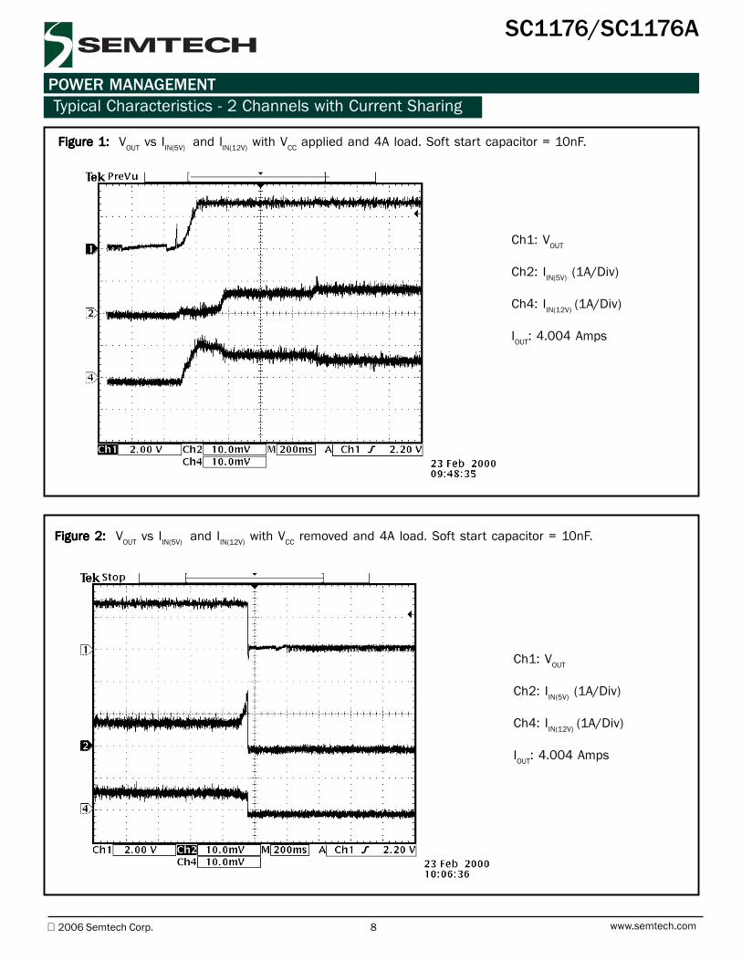
Typical Characteristics - 2 Channels with Current Sharing
Figure 1: Figure 1: Figure 1: Figure 1: Figure 1: VOUT vs IIN(5V) and IIN(12V) with VCC applied and 4A load. Soft start capacitor = 10nF.
Ch1: VOUT
Ch2: IIN(5V) (1A/Div)
Ch4: IIN(12V) (1A/Div)
IOUT: 4.004 Amps
Figure 2:Figure 2:Figure 2:Figure 2:Figure 2: VOUT vs IIN(5V) and IIN(12V) with VCC removed and 4A load. Soft start capacitor = 10nF.
Ch1: VOUT
Ch2: IIN(5V) (1A/Div)
Ch4: IIN(12V) (1A/Div)
IOUT: 4.004 Amps

9 2006 Semtech Corp. www.semtech.com
POWER MANAGEMENT
SC1176/SC1176A
Typical Characteristics - 2 Channels with Current Sharing (Cont.)
Figure 4: Figure 4: Figure 4: Figure 4: Figure 4: VOUT vs IIN(5V) and IIN(12V) with VCC removed and 12A load. Soft start capacitor = 10nF.
Ch1: VOUT
Ch2: IIN(5V) (2A/Div)
Ch4: IIN(12V) (2A/Div)
IOUT: 12 Amps
Figure 3:Figure 3:Figure 3:Figure 3:Figure 3: VOUT vs IIN(5V) and IIN(12V) with VCC applied and 12A load. Soft start capacitor = 10nF.
Ch1: VOUT
Ch2: IIN(5V) (2A/Div)
Ch4: IIN(12V) (2A/Div)
IOUT: 12 Amps

10 2006 Semtech Corp. www.semtech.com
POWER MANAGEMENT
SC1176/SC1176A
Typical Characteristics - 2 Channels with Current Sharing (Cont.)
The Current Sharing Evaluation Board is not intended for a specific application. The power components are notoptimized for minimum cost and size. This evaluation board should be used to understand the operation of theSC1176. To design with SC1176 for specific current sharing applications. Please refer to: Application note AN00-3.
Figure 5: Figure 5: Figure 5: Figure 5: Figure 5: Efficiency data - current sharing mode.
0.0
0.1
0.2
0.3
0.4
0.5
0.6
0.7
0.8
0.9
1.0
0 2 4 6 8 10 12 14Current (A)
Effic
ienc
y (%
)
VIN(MASTER) = 12VVIN(SLAVE) = 5VVOUT = 2.75V
11 2006 Semtech Corp. www.semtech.com
POWER MANAGEMENT
SC1176/SC1176A
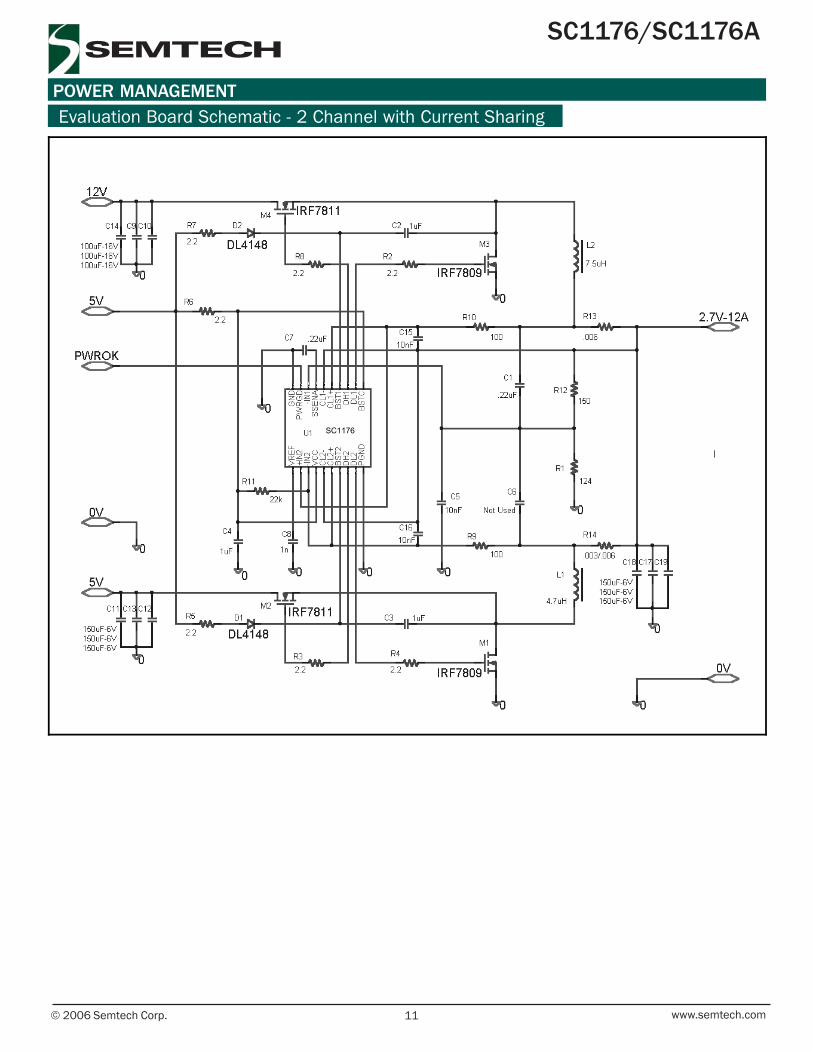
Evaluation Board Schematic - 2 Channel with Current Sharing
SC1176

12 2006 Semtech Corp. www.semtech.com
POWER MANAGEMENT
SC1176/SC1176A
metI ytitnauQ ecnerefeR traP
1 2 7C,1C V05,Fu22.
2 3 4C,3C,2C V05,Fu1
3 3 61C,51C,5C 10 V05,Fn
4 1 8C V05,Fn1
5 3 41C,01C,9C V6,Fu001
6 6 91C,81C,71C,31C,21C,11C V61,Fu051
7 2 2D,1D 8414LD
8 1 1L A8,Hu5.7
9 1 2L A8,Hu7.4
01 2 3M,1M 0307BDFro9087FRI
11 2 4M,2M 0307BDFro1187FRI
21 1 1R 421
31 7 8R,7R,6R,5R,4R,3R,2R 2.2
41 2 01R,9R 001
51 1 21R 051
61 1 31R 600.
71 1 41R 300.
81 1 1U 6711CS
Evaluation Board Bill of Materials - 2 Channels with Current Sharing

13 2006 Semtech Corp. www.semtech.com
POWER MANAGEMENT
SC1176/SC1176A
Top Side Traces
Bottom Side Traces
Evaluation Board Gerber Plots - 2 Channels with Current Sharing
14 2006 Semtech Corp. www.semtech.com
POWER MANAGEMENT
SC1176/SC1176A
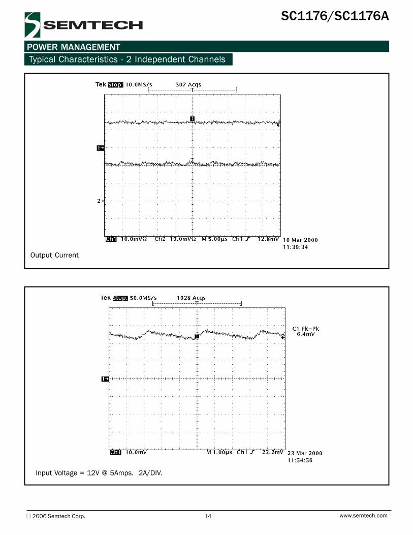
Output Current
Typical Characteristics - 2 Independent Channels
Input Voltage = 12V @ 5Amps. 2A/DIV.

15 2006 Semtech Corp. www.semtech.com
POWER MANAGEMENT
SC1176/SC1176A
Peak - Peak Output Ripple @ 5A
Input Voltage = 12V.Output Voltage = 2.0V
Typical Characteristics - 2 Independent Channels (Cont.)
Phase Node 12V Input @ 5A Phase Node 12V Input @ 5A Phase Node 12V Input @ 5A Phase Node 12V Input @ 5A Phase Node 12V Input @ 5A (without snubber and RC network.
16 2006 Semtech Corp. www.semtech.com
POWER MANAGEMENT
SC1176/SC1176A
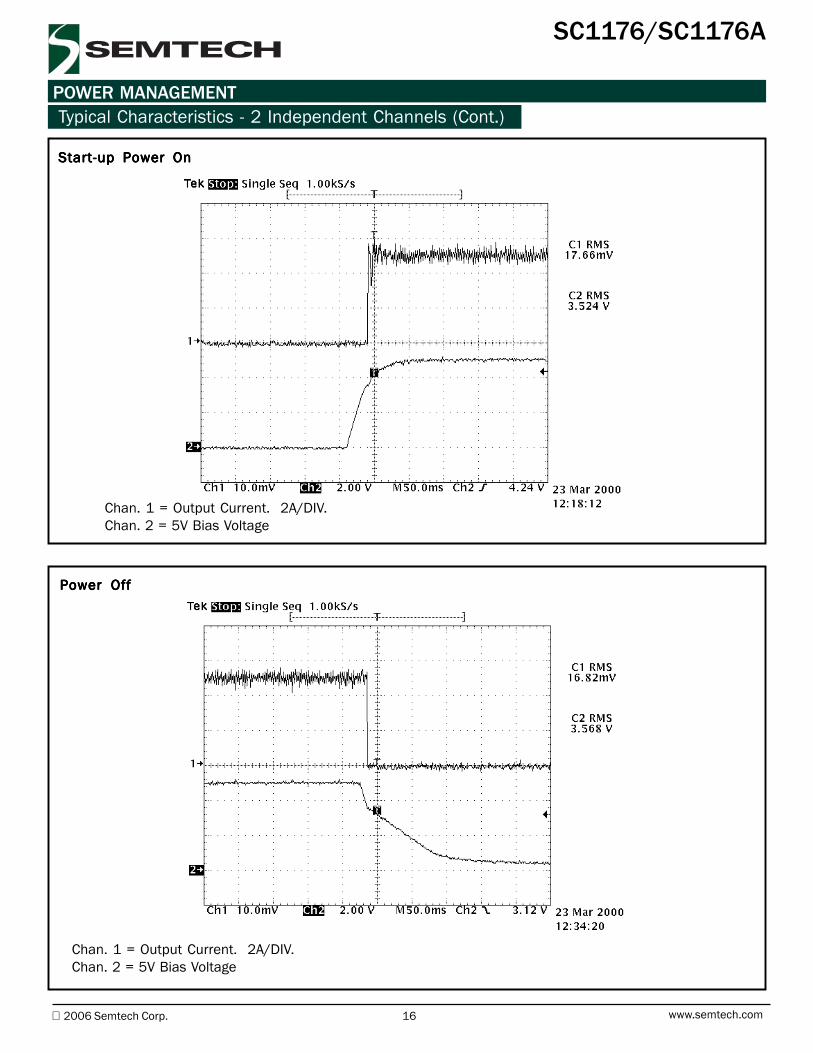
Start-up Power OnStart-up Power OnStart-up Power OnStart-up Power OnStart-up Power On
Chan. 1 = Output Current. 2A/DIV.Chan. 2 = 5V Bias Voltage
Power OffPower OffPower OffPower OffPower Off
Chan. 1 = Output Current. 2A/DIV.Chan. 2 = 5V Bias Voltage
Typical Characteristics - 2 Independent Channels (Cont.)
17 2006 Semtech Corp. www.semtech.com
POWER MANAGEMENT
SC1176/SC1176A
707580859095
100
0 1 2 3 4 5 6
OUTPUT CURRENT
EFFI
CIE
NC
Y
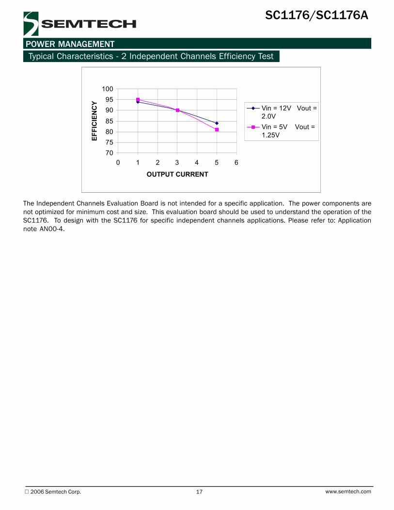
Vin = 12V Vout =2.0VVin = 5V Vout =1.25V
The Independent Channels Evaluation Board is not intended for a specific application. The power components arenot optimized for minimum cost and size. This evaluation board should be used to understand the operation of theSC1176. To design with the SC1176 for specific independent channels applications. Please refer to: Applicationnote AN00-4.
Typical Characteristics - 2 Independent Channels Efficiency Test

18 2006 Semtech Corp. www.semtech.com
POWER MANAGEMENT
SC1176/SC1176A
Evaluation Board Schematic - 2 Independent Channels

19 2006 Semtech Corp. www.semtech.com
POWER MANAGEMENT
SC1176/SC1176A
metI ytitnauQ ecnerefeR traP
1 3 3C,2C,1C V05,Fu1
2 3 11C,6C,4C V05,Fu22.
3 1 5C V05,Fn1
4 4 01C,9C,8C,7C V05,Fn01
5 9 02C,91C,81C,71C,61C,51C,41C,31C,21C V6,Fu051
6 3 32C,22C,12C V61,Fu001
7 2 2D,1D 8414LD
8 1 1L A8,Hu5.7
9 1 2L A8,Hu7.4
01 2 3M,1M 0307BDFro9087FRI
11 2 4M,2M 0307BDFro1187FRI
21 7 7R,6R,5R,4R,3R,2R,1R 2.2
31 3 31R,9R,8R 001
41 1 01R 600.
51 1 11R 022
61 1 21R 300.
71 2 51R,41R 421
81 1 1U 6711CS
Evaluation Board Bill of Materials - 2 Independent Channels

20 2006 Semtech Corp. www.semtech.com
POWER MANAGEMENT
SC1176/SC1176A
Top Side Traces
Bottom Side Traces
Evaluation Board Gerber Plots - 2 Independent Channels

21 2006 Semtech Corp. www.semtech.com
POWER MANAGEMENT
SC1176/SC1176A
Power and signal traces must be kept separated for noiseconsiderations. Feedback, current sense traces and ana-log ground should not cross any traces or planes carryinghigh switching currents, such as the input loop or thephase node.
The input loop, consisting of the input capacitors andboth MOSFETs must be kept as small as possible. All ofthe high switching currents occur in this loop. The en-closed loop area must be kept small to minimize induc-tance and radiated and conducted emissions. Designingfor minimum trace length is not always the best approach,often a more optimum layout can be achieved by keep-ing loop area constraints in mind.
It is important to keep gate lengths short, the IC must beclose to the power switches. This is more difficult in adual channel device than a single and requires that thetwo power paths run on either side of a centrally locatedcontroller.
Grounding requirements are always conflicting in a buckconverter, especially at high power, and the trick is toachieve the best compromise. Power ground (PGND)
should be returned to the bottom MOSFET source to pro-vide the best gate current return path. Analog ground(GND) should be returned to the ground side of the out-put capacitors so that the analog circuitry in the control-ler has an electrically quiet reference and to provide thegreatest feedback accuracy. The problem is that the dif-ferential voltage capability of the two IC grounds is lim-ited to about 1V for proper operation and so the physicalseparation between the two grounds must also be mini-mized. If the grounds are too far apart, fast current tran-sitions in the connection can generate voltage spikesexceeding the 1V capability, resulting in unstable and er-ratic behavior.
The feedback divider must be close to the IC and bereturned to analog ground. Current sense traces mustbe run parallel and close to each other and to analogground.
The IC must have a ceramic decoupling capacitor acrossits supply pins, mounted as close to the device as pos-sible. The small ceramic, noise-filtering capacitors on thecurrent sense lines should also be placed as close to theIC as possible.
Layout Guidelines
22 2006 Semtech Corp. www.semtech.com
POWER MANAGEMENT
SC1176/SC1176A
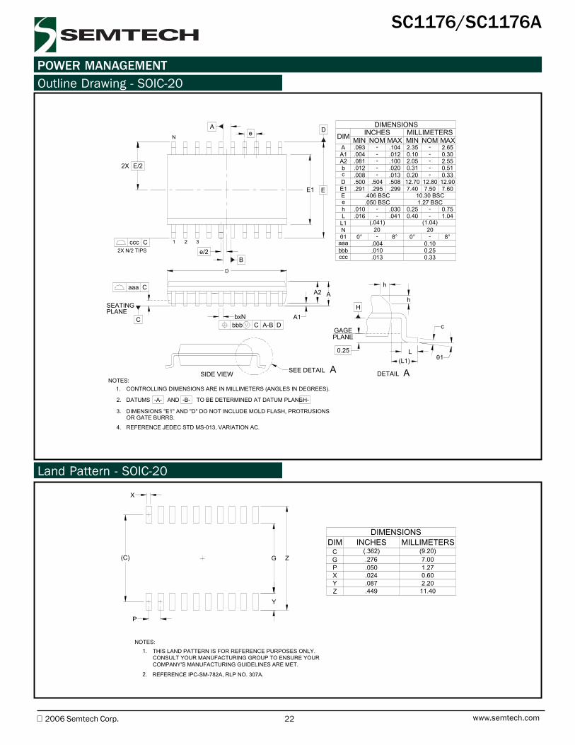
Outline Drawing - SOIC-20
01
ccc
aaabbb
MAX
DIMENSIONS
A1
e
L
NL1
h
c
E1E
D
bA2
MINDIMA
INCHESNOM
MILLIMETERSNOMMIN MAX
REFERENCE JEDEC STD MS-013, VARIATION AC.4.
E
.041
.013
.104
.100
.0122.35
-(1.04)
-
1.04
0.33
--- 2.65
2.550.30
.030.010 - 0.750.25 -
h
h
3. DIMENSIONS "E1" AND "D" DO NOT INCLUDE MOLD FLASH, PROTRUSIONSOR GATE BURRS.
-B-
CONTROLLING DIMENSIONS ARE IN MILLIMETERS (ANGLES IN DEGREES).
DATUMS AND TO BE DETERMINED AT DATUM PLANE
NOTES:1.
2. -A- -H-
SIDE VIEW
A
B
C
De
H
e/2
bbb C A-B D
SEE DETAIL A
L(L1)
0.25
PLANEGAGE c
01
(.041)
.013
-.004
-
-
--
-
0°
.016
.008
.081
.004
.093
8° 0°
0.33
0.10- 8°
0.40
0.20
2.050.10
.050 BSC
.406 BSC
20
.010
.291 .295
.012 -
20
0.25
1.27 BSC10.30 BSC
7.50
-
.299 7.40
.020 0.31
7.60
0.51
.504
2X N/2 TIPS
SEATING
aaa C
E/2
ccc C
2X
21 3
N
AA2
A1bxN
D
E1.500 12.70.508 12.80 12.90
PLANE
DETAIL A
THIS LAND PATTERN IS FOR REFERENCE PURPOSES ONLY.CONSULT YOUR MANUFACTURING GROUP TO ENSURE YOURCOMPANY'S MANUFACTURING GUIDELINES ARE MET.
NOTES:1.
REFERENCE IPC-SM-782A, RLP NO. 307A.2.
(.362) (9.20)ZG
Y
P
(C) 7.00.2761.27.0500.60.0242.20.08711.40.449
X
INCHESDIMENSIONS
Z
P
YX
DIMCG
MILLIMETERS
Land Pattern - SOIC-20

23 2006 Semtech Corp. www.semtech.com
POWER MANAGEMENT
SC1176/SC1176A
Outline Drawing - TSSOP-20
Land Pattern - TSSOP-20
L(L1)
c
01
GAGEPLANE
SEE DETAILDETAIL AA
0.25
.026 BSC
.252 BSC
20
.004
.169
.251.173.255
.007 -
20
0.10
0.65 BSC6.40 BSC
4.406.50
-
.177
.2594.306.40
.012 0.19
4.506.60
0.30
bxN
2X N/2 TIPS
SEATING
aaa C
E/2
INDICATORPIN 1
2X
1 32
N
E1
bbb C A-B D
ccc C
DIMENSIONS "E1" AND "D" DO NOT INCLUDE MOLD FLASH, PROTRUSIONS3.OR GATE BURRS.
DATUMS AND TO BE DETERMINED AT DATUM PLANE
CONTROLLING DIMENSIONS ARE IN MILLIMETERS (ANGLES IN DEGREES).
-B-
NOTES:1.
2. -A- -H-
SIDE VIEW
(.039)
.004
.008
-
.024
-
--
-
0
.018
.003
.031
.002-
8 0
0.20
0.10- 8
0.45
0.09
0.800.05
.030
.007
.047
.042
.006-
(1.0)0.60
-
0.75
0.20
--- 1.20
1.050.15
A
B
C
De
e/2
HPLANE
D
E
A1
A2 A
REFERENCE JEDEC STD MO-153, VARIATION AC.4.
INCHES
b
N
ccc
aaabbb
01
E1E
LL1
e
Dc
A2A1
DIMA
MIN MAXMILLIMETERSMIN
DIMENSIONS
NOM MAX NOM
Semtech CorporationPower Management Products Division200 Flynn Road, Camarillo, CA 93012
Phone: (805)498-2111 FAX (805)498-3804
Contact Information
(.222) (5.65)ZG
Y
P
(C) 4.10.1610.65.0260.40.0161.55.0617.20.283
X
INCHESDIMENSIONS
Z
P
YX
DIMCG
MILLIMETERS
THIS LAND PATTERN IS FOR REFERENCE PURPOSES ONLY.CONSULT YOUR MANUFACTURING GROUP TO ENSURE YOURCOMPANY'S MANUFACTURING GUIDELINES ARE MET.
NOTES:1.

Mouser Electronics
Authorized Distributor
Click to View Pricing, Inventory, Delivery & Lifecycle Information: Semtech:
SC1176CSWTRT SC1176ASWTRT SC1176TSTRT