Embed Size (px)
Citation preview

www.apexanalog.com© Apex Microtechnology Inc
All rights reserved
Power Operational Am
MP108 • MP108A
plifier
FEATURES
• Low Cost • High Voltage - 200V• High Output Current - 10A• 100W Dissipation Capability• 300 kHz Power Bandwidth
APPLICATIONS
• Inkjet Printer Head Drive• Piezo Transducer Drive• Industrial Instrumentation• Reflectometers• Ultra-Sound Transducer Drive
DESCRIPTION
The MP108 operational amplifier is a surface mount constructed component that provides a cost effec-tive solution in many industrial applications. The MP108 offers outstanding performance that rivals muchmore expensive hybrid components yet has a footprint of only 4 sq in. The MP108 has many optional featuressuch as four-wire current limit sensing and external compensation. The 300 kHz power bandwidth and 10Aoutput of the MP108 makes it a good choice for piezo transducer drive applications. The MP108 is built on athermally conductive but electrically insulating substrate that can be mounted to a heat sink.
Figure 1: Equivalent Schematic
8+VB
+VB
GNDBPLT
4
32
1TPSUBSTRATE BACKPLATE
5CC1
CC2 6
34
33
32
30
25
-IN
+IN
GND
-VB
-VB
141516
111213
28
27
202122
171819
+VS
+VS
+VS
+OUT+OUT+OUT
-OUT
-VS
-OUT
-OUT
-VS
-VS
C1 R1 R2
C5
Q1A Q1B
Q17
Q2
R3
Q4D1
Q7
Q8
Q6
R15
Q12 Q13
Q15A Q15B
R10 R11
R12
Q23
R19C3
Q24
R20
Q21
Q18Q19
Q20
IC1
R8
R7
Q14
Q11
Q16
D2
Q9
R17 Q22
Q3R5
R9
+CL
-CL
. Oct 2016MP108U Rev H
MP108 • MP108A
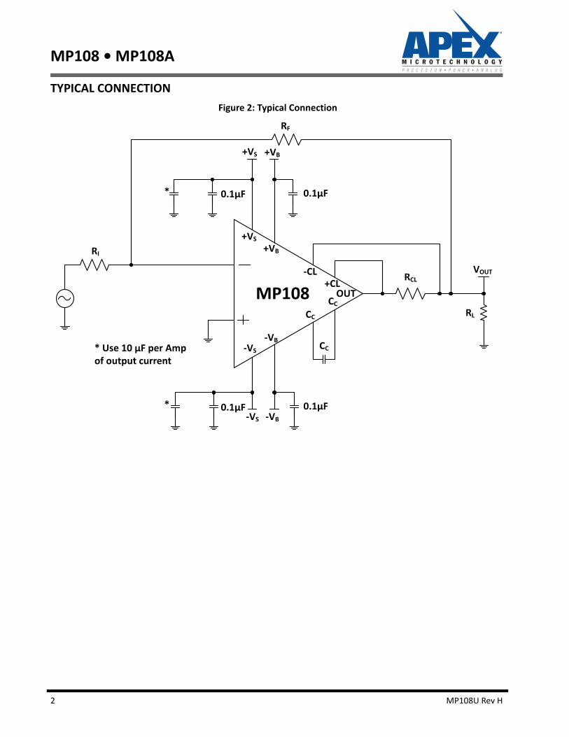
TYPICAL CONNECTION
Figure 2: Typical Connection
+VS+VB
-CL+CL
OUTMP108CC
-VS
-VB
RCL
+VS
RF
CC
CC
-VB-VS0.1μF 0.1μF
0.1μF 0.1μF
+VB
VOUT
RI
RL
*
*
* Use 10 μF per Amp of output current
2 MP108U Rev H

MP108 • MP108A
EXTERNAL CONNECTIONS
Figure 3: Pin-out
Pin Number Name Description
1 TP Apex test pin, do not connect.
2 BPLT AC coupling to backplate. Connect to signal ground.
3, 32 GNDGround. Pins 3 and 32 are not connected on the unit. Connect both pins to system
signal ground.
4, 8 +VB The positive boost supply rail. Short to +Vs if unused. See applicable section.
5, 6 CCCompensation capacitor connection. Select value based on Phase Compensation.
See applicable section.
11, 12, 13 +OUTThe positive current output. Short to -OUT pins. Connect these pins to the MP108 side of the current limit resistor and the +CL pin. Output current is sourced from
these pins through the current limit resistor to the load.
14, 15, 16 +Vs The positive supply rail.
17, 18, 19 -Vs The negative supply rail.
20, 21, 22 -OUTThe negative current output. Short to +OUT pins. Connect these pins to the MP108 side of the current limit resistor and the +CL pin. Output current sinks to these pins
through the current limit resistor from the load.
25, 30 -VB The negative boost supply rail. Short to -Vs if unused. See applicable section.
27 -CLConnect to the load side of the current limit resistor and feedback resistor. Current
limit will activate as the voltage across RCL exceeds 0.65 V.
28 +CLConnect to the OUT side of the current limit resistor. Current limit will activate as
the voltage across RCL exceeds 0.65 V.
33 +IN The non-inverting input.
34 -IN The inverting input.
All Others NC No connection.
12
3
4
5
6
7
89
10
11
12
13
141516
3130
29
2827
25
2423
22
21
2019
1817
32
26
TPBPLT
GND
CC1
CC2
NC
+VB
NC
NC
+OUT
+OUT
+OUT
+VS
+VS
+VS
-IN
+IN
-VB
NC
+CL-CL
NC
-VB
NC
NC-OUT
-OUT
-OUT
-VS
-VS
33
NCGND
34
+VB
-VS
MP108(Viewed from
backplate)
MP108U Rev H 3
MP108 • MP108A
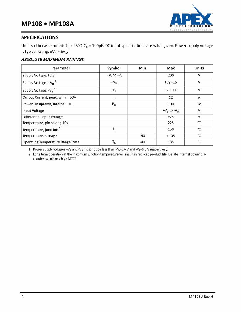
SPECIFICATIONS
Unless otherwise noted: TC = 25°C, CC = 100pF. DC input specifications are value given. Power supply voltage
is typical rating. ±VB = ±VS.
ABSOLUTE MAXIMUM RATINGS
Parameter Symbol Min Max Units
Supply Voltage, total +Vs to -Vs 200 V
Supply Voltage, +VB 1
1. Power supply voltages +VB and -VB must not be less than +Vs-0.6 V and -VS+0.6 V respectively.
+VB +VS +15 V
Supply Voltage, -VB 1 -VB -VS -15 V
Output Current, peak, within SOA IO 12 A
Power Dissipation, internal, DC PD 100 W
Input Voltage +VB to -VB V
Differential Input Voltage ±25 V
Temperature, pin solder, 10s 225 °C
Temperature, junction 2
2. Long term operation at the maximum junction temperature will result in reduced product life. Derate internal power dis-sipation to achieve high MTTF.
TJ 150 °C
Temperature, storage -40 +105 °C
Operating Temperature Range, case TC -40 +85 °C
4 MP108U Rev H
MP108 • MP108A
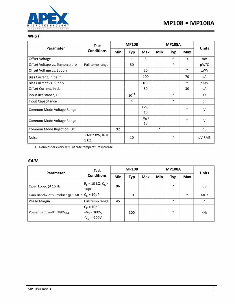
INPUT
GAIN
ParameterTest
Conditions
MP108 MP108AUnits
Min Typ Max Min Typ Max
Offset Voltage 1 5 * 3 mV
Offset Voltage vs. Temperature Full temp range 50 * µV/°C
Offset Voltage vs. Supply 20 * µV/V
Bias Current, initial 1
1. Doubles for every 10°C of case temperature increase
100 70 pA
Bias Current vs. Supply 0.1 * pA/V
Offset Current, initial 50 30 pA
Input Resistance, DC 1011 * Ω
Input Capacitance 4 * pF
Common Mode Voltage Range+VB -
15* V
Common Mode Voltage Range-VB +
15* V
Common Mode Rejection, DC 92 * dB
Noise1 MHz BW, RS =
1 kΩ10 * µV RMS
ParameterTest
Conditions
MP108 MP108AUnits
Min Typ Max Min Typ Max
Open Loop, @ 15 HzRL = 10 kΩ, CC =
10pF96 * dB
Gain Bandwidth Product @ 1 MHz CC = 10pF 10 * MHz
Phase Margin Full temp range 45 * °
Power Bandwidth 180VP-P
CC = 10pF,
+VS = 100V,
-VS = -100V
300 * kHz
MP108U Rev H 5

MP108 • MP108A
OUTPUT
POWER SUPPLY
THERMAL
Note: *The specification of MP108A is identical to the specification for MP108 in the applicable column tothe left.
ParameterTest
Conditions
MP108 MP108AUnits
Min Typ Max Min Typ Max
Voltage Swing IO = 10A +VS - 10 +VS- 8.6 * * V
Voltage Swing IO = -10A -VS + 10 -VS + 7 * * V
Voltage SwingIO = 10A,
+VB = +VS +10V
+VS -
1.6* V
Voltage SwingIO = -10A,
-VB = -VS -10V
-VS +
5.1* V
Current, Continuous, DC 10 11 A
Slew Rate, A V = -20 CC= 10pF 150 170 * * V/µs
Settling Time to 0.1% 2V step 1 * µs
Resistance No load, DC 5 * Ω
ParameterTest
Conditions
MP108 MP108AUnits
Min Typ Max Min Typ Max
Voltage ±15 ±75 ±100 * * * V
Current, quiescent 50 65 * * mA
ParameterTest
Conditions
MP108 MP108AUnits
Min Typ Max Min Typ Max
Resistance, AC, junction to case 1
1. Rating applies if the output current alternates between both output transistors at a rate faster than 60 Hz.
Full temp range, F ≥ 60 Hz
1 * °C/W
Resistance, DC, junction to caseFull temp range, F < 60 Hz
1.25 * °C/W
Resistance, junction to air Full temp range 13 * °C/W
Temperature Range, case -40 +85 * * °C
6 MP108U Rev H

MP108 • MP108A
TYPICAL PERFORMANCE GRAPHS
Figure 4: Power Derating Figure 5: Phase Response W/ Boost
Figure 6: Phase Response W/O Boost Figure 7: Small Signal Response W/ Boost
100
80
60
40
20
00 20-20 40 80 10060
Case Temperature, TC (°C)
)
-40
90
120
150
180
210100k
23
1
1M 5M
Frequency, F (Hz)
Phas
e,
1 CC = 10pF2 CC = 33pF3 CC = 100pFRLIO = 1A
2
1
90
120
150
180300k
23
1
1M 10M
Frequency, F (Hz)
Phas
e,
2
1
1 CC = 10pF2 CC = 33pF3 CC = 100pFRLIO = 1A
120
100
80
60
40
20
1M0
1 10 100 1k 10k 10M100k
Frequency, F (Hz)
Ope
n Lo
op G
ain,
A (d
B) CC = 33pF
CC = 220pF
CC = 470pF
RLIO = 1A
MP108U Rev H 7

MP108 • MP108A
Figure 8: Small Signal Response W/O Boost
Figure 9: Power Response
Figure 10: Current Limit Figure 11: Quiescent Current vs. Supply
120
100
80
60
40
20
1M0
1 10 100 1k 10k 100k
Frequency, F (Hz)
Ope
n Lo
op G
ain,
A (d
B)
CC = 10pF
CC = 33pF
CC = 100pF
RLIO = 1A DC
200
100
010k 100k 1M 5M
Frequency, F (Hz)
Out
put V
olta
ge, V
o (V
P-P)
CC = 470pF
CC = 10pF
CC = 33pF
CC = 100pF
CC = 220pF
130
120
110
100
90
80
70-50 -25 0 25 50 10075
Case Temperature, TC (°C)
Nor
mal
ized
Curr
ent L
imit
(%)
120
100
80
60
400 40 80 120 160 200
Total Supply Voltage, VS (V)
Nor
mal
ized
Qui
esce
nt C
urre
nt, I
o (%
)
TC = 85°C
TC = 25°CTC = -40°C
8 MP108U Rev H
MP108 • MP108A
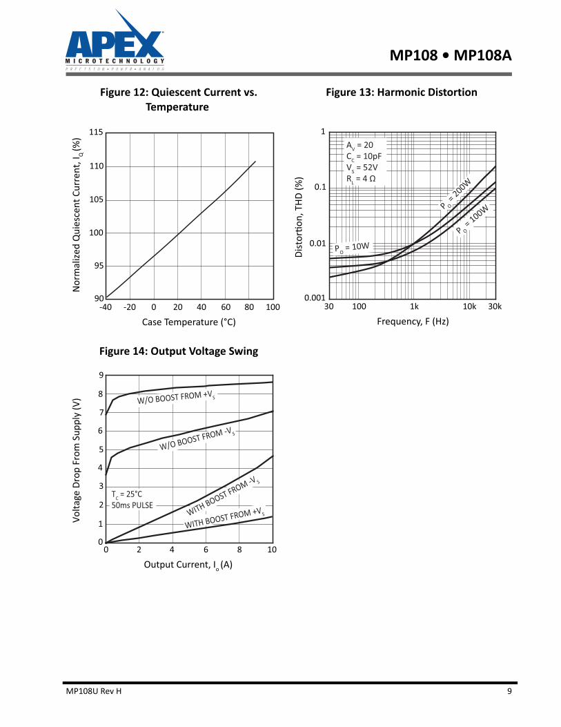
Figure 12: Quiescent Current vs. Temperature
Figure 13: Harmonic Distortion
Figure 14: Output Voltage Swing
115
110
105
100
95
90-20 0 20 40 60 10080
Case Temperature (°C)
Nor
mal
ized
Qui
esce
nt C
urre
nt, I
Q (%
)
-40
1
0.1
0.01
0.00130 100 1k 30k10k
Frequency, F (Hz)
)
PO = 10W
AV = 20CC = 10pFVS = 52VRL
P O = 200W
P O = 100W
9
8
7
6
5
4
3
2
1
0 2 4 6 8 10
Output Current, Io (A)
Volta
ge D
rop
From
Sup
ply
(V) W/O BOOST FROM +VS
WITH BOOST FROM +VSWITH BOOST FROM -V S
TC = 25°C50ms PULSE
W/O BOOST FROM -VS
0
MP108U Rev H 9

MP108 • MP108A
SAFE OPERATING AREA (SOA)
The MOSFET output stage of the MP108 is not limited by second breakdown considerations as in bipolaroutput stages. Only thermal considerations and current handling capabilities limit the SOA. The output stageis protected against transient flyback by the parasitic body diodes of the output stage MOSFET structure.However, for protection against sustained high energy flyback external fast reverse recovery diodes must beused.
Figure 15: SOA
20
10
1
0.21 10 200100
VS - Vo(V)
V S V S
(A)
C =85°C
C =25°CC =25°C
C =25°C
10 MP108U Rev H
MP108 • MP108A
GENERAL
Please read Application Note 1 “General Operating Considerations” which covers stability, supplies, heatsinking, mounting, current limit, SOA interpretation, and specification interpretation. Visit www.apexana-log.com for Apex Microtechnology’s complete Application Notes library, Technical Seminar Workbook, andEvaluation Kits.
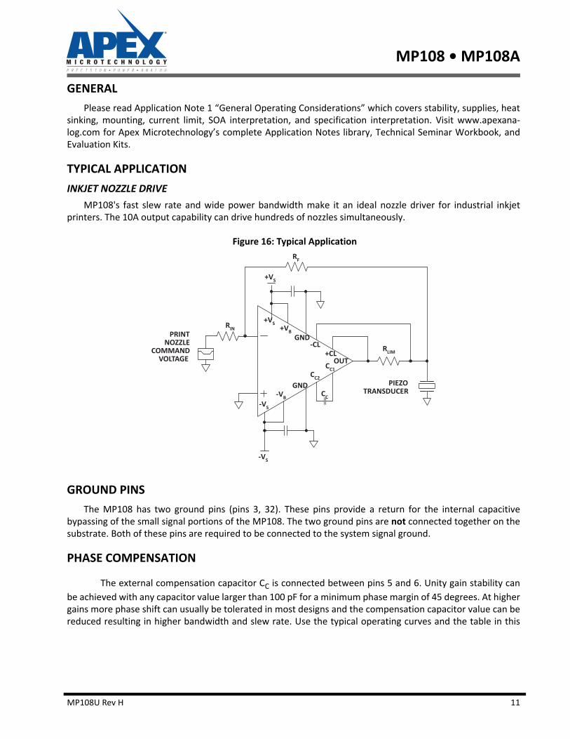
TYPICAL APPLICATION
INKJET NOZZLE DRIVE
MP108's fast slew rate and wide power bandwidth make it an ideal nozzle driver for industrial inkjetprinters. The 10A output capability can drive hundreds of nozzles simultaneously.
Figure 16: Typical Application
GROUND PINS
The MP108 has two ground pins (pins 3, 32). These pins provide a return for the internal capacitivebypassing of the small signal portions of the MP108. The two ground pins are not connected together on thesubstrate. Both of these pins are required to be connected to the system signal ground.
PHASE COMPENSATION
The external compensation capacitor CC is connected between pins 5 and 6. Unity gain stability can
be achieved with any capacitor value larger than 100 pF for a minimum phase margin of 45 degrees. At highergains more phase shift can usually be tolerated in most designs and the compensation capacitor value can bereduced resulting in higher bandwidth and slew rate. Use the typical operating curves and the table in this
MP108U Rev H 11
MP108 • MP108A
section as a guide to select CC for the application. An NPO (COG) type capacitor is required rated for the full
supply voltage (200 V).
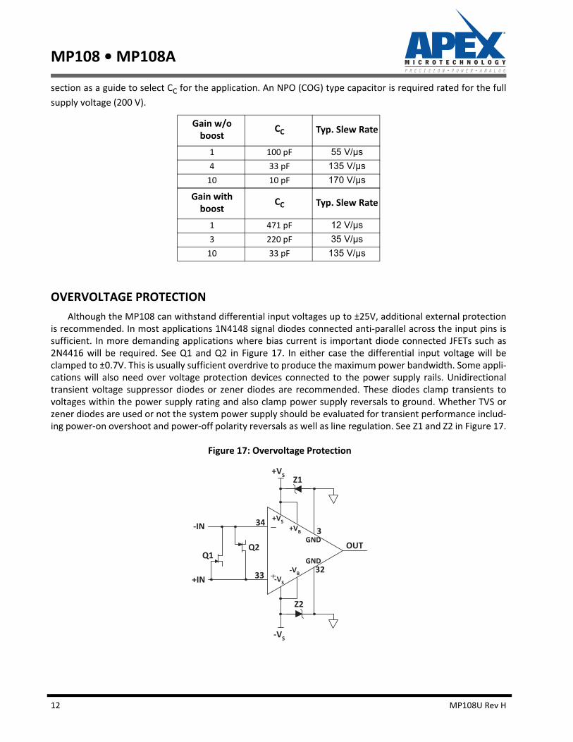
OVERVOLTAGE PROTECTION
Although the MP108 can withstand differential input voltages up to ±25V, additional external protectionis recommended. In most applications 1N4148 signal diodes connected anti-parallel across the input pins issufficient. In more demanding applications where bias current is important diode connected JFETs such as2N4416 will be required. See Q1 and Q2 in Figure 17. In either case the differential input voltage will beclamped to ±0.7V. This is usually sufficient overdrive to produce the maximum power bandwidth. Some appli-cations will also need over voltage protection devices connected to the power supply rails. Unidirectionaltransient voltage suppressor diodes or zener diodes are recommended. These diodes clamp transients tovoltages within the power supply rating and also clamp power supply reversals to ground. Whether TVS orzener diodes are used or not the system power supply should be evaluated for transient performance includ-ing power-on overshoot and power-off polarity reversals as well as line regulation. See Z1 and Z2 in Figure 17.
Figure 17: Overvoltage Protection
Gain w/o boost
CC Typ. Slew Rate
1 100 pF 55 V/µs
4 33 pF 135 V/µs
10 10 pF 170 V/µs
Gain with boost
CC Typ. Slew Rate
1 471 pF 12 V/µs
3 220 pF 35 V/µs
10 33 pF 135 V/µs
12 MP108U Rev H
MP108 • MP108A
POWER SUPPLY BYPASSING
Bypass capacitors to power supply terminals +VS and -VS must be connected physically close to the pins
to prevent local parasitic oscillation in the output stage of the MP108. Use electrolytic capacitors at least10µF per output amp required. Bypass the electrolytic capacitors with high quality ceramic capacitors (X7R)0.1µF or greater. In most applications power supply terminals +VB and -VB will be connected to +VS and -VS
respectively. Supply voltages +VB and -VB are bypassed internally but both ground pins 3 and 32 must be con-
nected to the system signal ground to be effective. In all cases power to the buffer amplifier stage of theMP108 at pins 8 and 25 must be connected to +VB and -VB at pins 4 and 30 respectively. Provide local bypass
capacitors at pins 8 and 25. See figure 2 for Typical Connection Diagram.
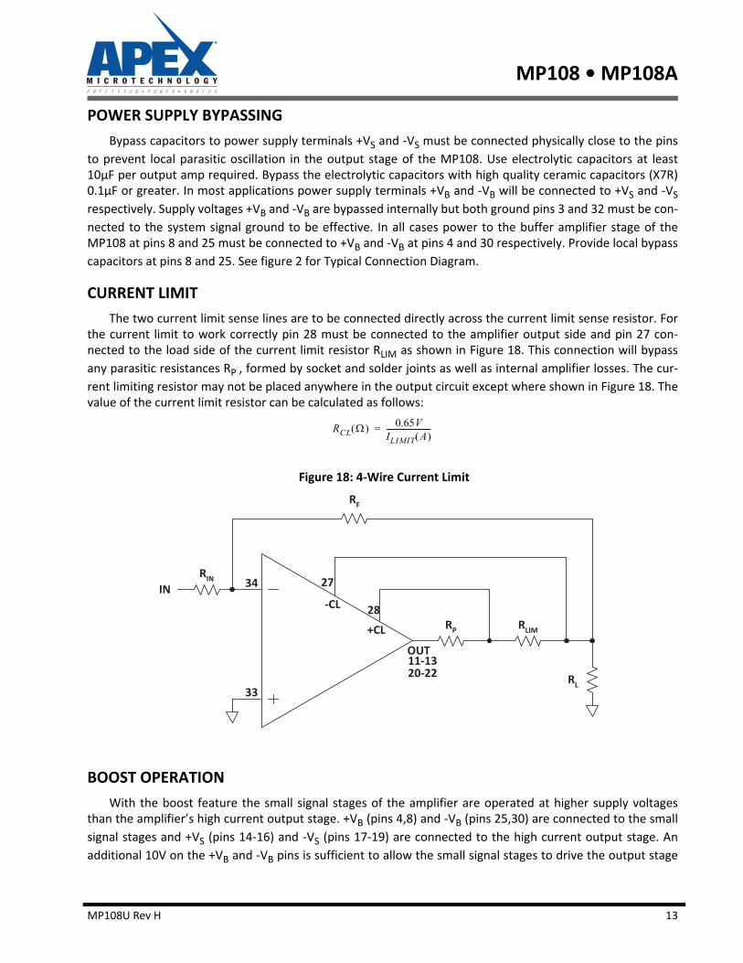
CURRENT LIMIT
The two current limit sense lines are to be connected directly across the current limit sense resistor. Forthe current limit to work correctly pin 28 must be connected to the amplifier output side and pin 27 con-nected to the load side of the current limit resistor RLIM as shown in Figure 18. This connection will bypass
any parasitic resistances RP , formed by socket and solder joints as well as internal amplifier losses. The cur-
rent limiting resistor may not be placed anywhere in the output circuit except where shown in Figure 18. Thevalue of the current limit resistor can be calculated as follows:
Figure 18: 4-Wire Current Limit
BOOST OPERATION
With the boost feature the small signal stages of the amplifier are operated at higher supply voltagesthan the amplifier’s high current output stage. +VB (pins 4,8) and -VB (pins 25,30) are connected to the small
signal stages and +VS (pins 14-16) and -VS (pins 17-19) are connected to the high current output stage. An
additional 10V on the +VB and -VB pins is sufficient to allow the small signal stages to drive the output stage
RCL 0.65VILIMIT A ------------------------=
MP108U Rev H 13

MP108 • MP108A
into the triode region and improve the output voltage swing for extra efficient operation when required.When the boost feature is not needed +VS and -VS are connected to the +VB and -VB pins respectively. The
+VB and -VB pins must not be operated at supply voltages less than +VS-0.6 V and -VS+0.6 V respectively.
BACKPLATE GROUNDING
The substrate of the MP108 is an insulated metal substrate. It is required that it be connected to signalground. Connect pin 2 (back plate) to signal ground. The back plate will then be AC grounded to signal groundthrough a 1µF capacitor.
14 MP108U Rev H
MP108 • MP108A
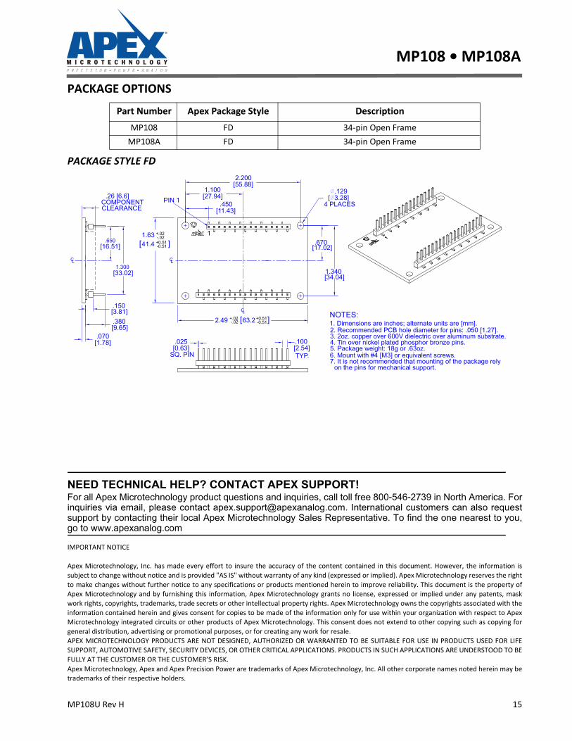
PACKAGE OPTIONS
PACKAGE STYLE FD
Part Number Apex Package Style Description
MP108 FD 34-pin Open Frame
MP108A FD 34-pin Open Frame
.070 [1.78]
.150 [3.81].380
[9.65]
1.300 [33.02]
.650 [16.51]
CL
.025 [0.63]SQ. PIN
.100 [2.54] TYP.
LC
LC
.26 [6.6]COMPONENTCLEARANCE
PIN 1.129
[ 3.28]4 PLACES
2.49 +.02-.02 [63.2+0.51
-0.51]
.670 [17.02]
1.340 [34.04]
.450 [11.43]
1.100 [27.94]
2.200 [55.88]
1. Dimensions are inches; alternate units are [mm].2. Recommended PCB hole diameter for pins: .050 [1.27].3. 2oz. copper over 600V dielectric over aluminum substrate.4. Tin over nickel plated phosphor bronze pins.5. Package weight: 18g or .63oz.6. Mount with #4 [M3] or equivalent screws.7. It is not recommended that mounting of the package rely on the pins for mechanical support.
NOTES:
1.63 +.02-.02
[41.4 +0.51-0.51 ]
1
MP108U Rev H 15
NEED TECHNICAL HELP? CONTACT APEX SUPPORT! For all Apex Microtechnology product questions and inquiries, call toll free 800-546-2739 in North America. Forinquiries via email, please contact [email protected]. International customers can also requestsupport by contacting their local Apex Microtechnology Sales Representative. To find the one nearest to you,go to www.apexanalog.com
IMPORTANT NOTICE
Apex Microtechnology, Inc. has made every effort to insure the accuracy of the content contained in this document. However, the information is
subject to change without notice and is provided "AS IS" without warranty of any kind (expressed or implied). Apex Microtechnology reserves the right
to make changes without further notice to any specifications or products mentioned herein to improve reliability. This document is the property ofApex Microtechnology and by furnishing this information, Apex Microtechnology grants no license, expressed or implied under any patents, mask
work rights, copyrights, trademarks, trade secrets or other intellectual property rights. Apex Microtechnology owns the copyrights associated with the
information contained herein and gives consent for copies to be made of the information only for use within your organization with respect to ApexMicrotechnology integrated circuits or other products of Apex Microtechnology. This consent does not extend to other copying such as copying for
general distribution, advertising or promotional purposes, or for creating any work for resale.
APEX MICROTECHNOLOGY PRODUCTS ARE NOT DESIGNED, AUTHORIZED OR WARRANTED TO BE SUITABLE FOR USE IN PRODUCTS USED FOR LIFESUPPORT, AUTOMOTIVE SAFETY, SECURITY DEVICES, OR OTHER CRITICAL APPLICATIONS. PRODUCTS IN SUCH APPLICATIONS ARE UNDERSTOOD TO BE
FULLY AT THE CUSTOMER OR THE CUSTOMER’S RISK.
Apex Microtechnology, Apex and Apex Precision Power are trademarks of Apex Microtechnology, Inc. All other corporate names noted herein may betrademarks of their respective holders.