Embed Size (px)
Citation preview
8/9/2019 POWER OPTIMIZED PROGRAMMABLE EMBEDDED CONTROLLER
http://slidepdf.com/reader/full/power-optimized-programmable-embedded-controller 1/11
International Journal of Computer Networks & Communications (IJCNC), Vol.2, No.4, July 2010
DOI : 10.5121/ijcnc.2010.2409 97
POWER OPTIMIZED PROGRAMMABLEEMBEDDED
CONTROLLER
M.Kamaraju1
Dr.K.Lal Kishore2
Dr.A.V.N.Tilak 3
1Dept. of ECE, Gudlavalleru Engineering College, Gudlavalleru - [email protected]
2Director,SIT, Jawarlal Nehru Technological University ,Hyderabad- [email protected]
3Dept. of ECE,Gudlavalleru Engineering College, Gudlavalleru - [email protected]
A BSTRACT
Now a days, power has become a primary consideration in hardware design, and is critical in computer
systems especially for portable devices with high performance and more functionality. Clock-gating is the
most common technique used for reducing processor’s power. In this work clock gating technique is
applied to optimize the power of fully programmable Embedded Controller (PEC) employing RISC
architecture. The CPU designed supports i) smart instruction set, ii) I/O port, UART iii) on-chip clocking
to provide a range of frequencies , iv) RISC as well as controller concepts. The whole design is captured
using VHDL and is implemented on FPGA chip using Xilinx .The architecture and clock gating
technique together is found to reduce the power consumption by 33.33% of total power consumed by this
chip.
K EYWORDS
Power, Clock Gating, RISC, FPGA, Xilinx
1. INTRODUCTION Low power consumption in embedded systems [1] has become a key factor for manyapplications. Portable applications, needing long battery life together with highpeak- performance, are demanding a very careful design at all levels.
The most important factor contributing to the energy consumption is the switching activity [2][3] .Once the technology and supply voltage have been set , major energy savings come fromthe careful minimization of switching activity.
While some switching activity is functional, i.e. it is required to propagate and manipulateinformation; there is a substantial amount of unnecessary activity in almost all digital circuits.Unnecessary switching activity arises from spurious transitions [4] due to unequal propagationdelays (glitches) and transitions occurring within units that are not participating in acomputation. One way to avoid these activities is by dynamically turning off the clock[5] tounused logic or peripherals .
Existing microprocessors [6], especially in the category of microcontrollers, often have thecapability of partially gating the clock signal when they fetch and execute NOP or otherminimal-activity instructions and also when a peripheral is powered-down. This does not totallyeliminate spurious power consumption. Other processors [7] can enter low-power operatingmodes, disabling the clock signal generator (Xtal oscillator and PLL). However, this is not

8/9/2019 POWER OPTIMIZED PROGRAMMABLE EMBEDDED CONTROLLER
http://slidepdf.com/reader/full/power-optimized-programmable-embedded-controller 2/11
International Journal of Computer Networks & Communications (IJCNC), Vol.2, No.4, July 2010
98
totally efficient in important applications. In [8] optimization of power is achieved by takingassistance of compiler while executing instructions. However hardware approach proposed inthis work reduces the power without compromising speed performance of the chip.
In the proposed PEC, the control unit is designed to have the capability of gating the clock signal when they fetch and execute instructions. On-chip clocking [9] mechanism is employedto synchronize with on-chip peripherals/memory and with the external bus. For poweroptimization of integrated circuits it is relevant to understand the causes of power dissipation.Clock power[10] dominates the total power consumed by a microcontroller as the clock is fed tomost of the circuit blocks. Charge/discharge power given by P = f CL Vdd Vs, dominates the totalpower dissipation of the chip. The frequency f of the clock cannot be reduced as it effects thespeed of the chip. When output swings from 0 to Vdd then P varies as square Vdd .However lowering P by reducing power supply voltage to 2V or less is found to lead toseveral problems[11] [12] like decrease in drivability of MOSFET and increase in gate delaytime.
2. PROGRAMMABLE EMBEDDED CONTROLLER ARCHITECTURE
Architecture of PEC is shown in Figure.1. Various blocks in the architecture are register file,
ALU, RAM, ROM, UART, I/O Ports, BCD to 7 segment driver , Control unit, and clocker,designed to perform particular task. Register File is a set of registers that are modeled as RAMof 16 bit words, used to store intermediate values during instruction processing. The ALUperforms 16 bit operations. The Read Only Memory (ROM) is 256 bytes with 16 bit wordlength and is used to store the instruction data. The Random Access Memory (RAM) 1K×16 isused to store temporary data. Port 0 and Port 1 are two ports which are configured as output andinput ports respectively.
A display driver for BCD to 7 segment display is designed to drive the 7 segment display unit.The control unit generates various control signals to all other blocks to execute desired task specified by the instructions. The PEC is initiated by the reset signal whenever reset signalasserts high, the controller generate appropriate signals to load the PC address of the ROM. Theexternal interrupt mechanism activates on any hardware interrupt or reset signal arriving at the
controller when it is in idle mode.
2.1. On-Chip Clocking Mechanism
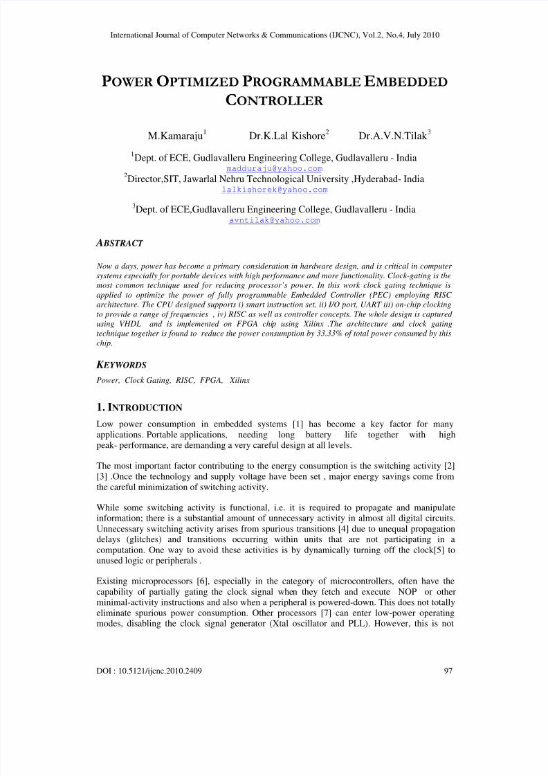
The frequency of the application specific hardwired oscillator shown in Figure.2 isprogrammable by means of the 4-bit number (control word value) contained in the dedicatedregister r_osc. On-chip clocking is used to obtain different frequencies ranging from 44 MHz to134 MHz by changing the control word values as shown in Figure. 3.

8/9/2019 POWER OPTIMIZED PROGRAMMABLE EMBEDDED CONTROLLER
http://slidepdf.com/reader/full/power-optimized-programmable-embedded-controller 3/11
International Journal of Computer Networks & Communications (IJCNC), Vol.2, No.4, July 2010
99
Figure.1 Architecture of Programmable Embedded Controller
Figure.2 Oscillator Circuit
8/9/2019 POWER OPTIMIZED PROGRAMMABLE EMBEDDED CONTROLLER
http://slidepdf.com/reader/full/power-optimized-programmable-embedded-controller 4/11
International Journal of Computer Networks & Communications (IJCNC), Vol.2, No.4, July 2010
100
Figure.3 Oscillator Cycle Time vs. Control Word Value
2.2. Clock Gating
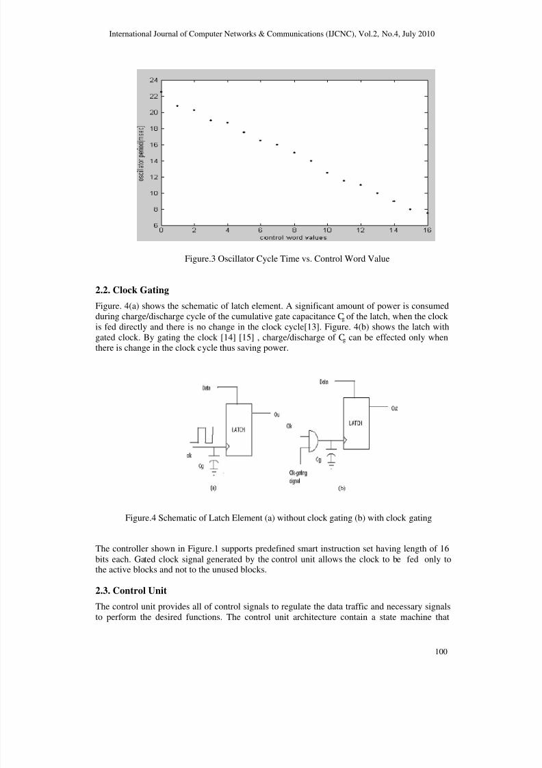
Figure. 4(a) shows the schematic of latch element. A significant amount of power is consumedduring charge/discharge cycle of the cumulative gate capacitance Cg of the latch, when the clock is fed directly and there is no change in the clock cycle[13]. Figure. 4(b) shows the latch withgated clock. By gating the clock [14] [15] , charge/discharge of Cg can be effected only whenthere is change in the clock cycle thus saving power.
Figure.4 Schematic of Latch Element (a) without clock gating (b) with clock gating
The controller shown in Figure.1 supports predefined smart instruction set having length of 16bits each. Gated clock signal generated by the control unit allows the clock to be fed only tothe active blocks and not to the unused blocks.
2.3. Control Unit
The control unit provides all of control signals to regulate the data traffic and necessary signalsto perform the desired functions. The control unit architecture contain a state machine that

8/9/2019 POWER OPTIMIZED PROGRAMMABLE EMBEDDED CONTROLLER
http://slidepdf.com/reader/full/power-optimized-programmable-embedded-controller 5/11
International Journal of Computer Networks & Communications (IJCNC), Vol.2, No.4, July 2010
101
causes all appropriate signal values to update based on current state and input signals andproduce a next state for state machine. The control unit performs two processes. The first is acombinational process (not clocked) that examines the current state and all inputs and producesoutput control signals and next state output. The second is the sequential process (having aclock) that is used to store the current state and copy of the next state to the current state.
Figure.5 Signals of Control Unit
If the reset signal is high the sequential process set the current state value to reset1, the firststate of the reset sequence. The logic for clock gating is implemented within the control unit.The controller generate appropriate clock gating signal to reduce power consumption of thechip. When the control unit decodes the opcode of the instruction, the control unit generatescontrol signals as shown in Figure.5, to execute the instruction.
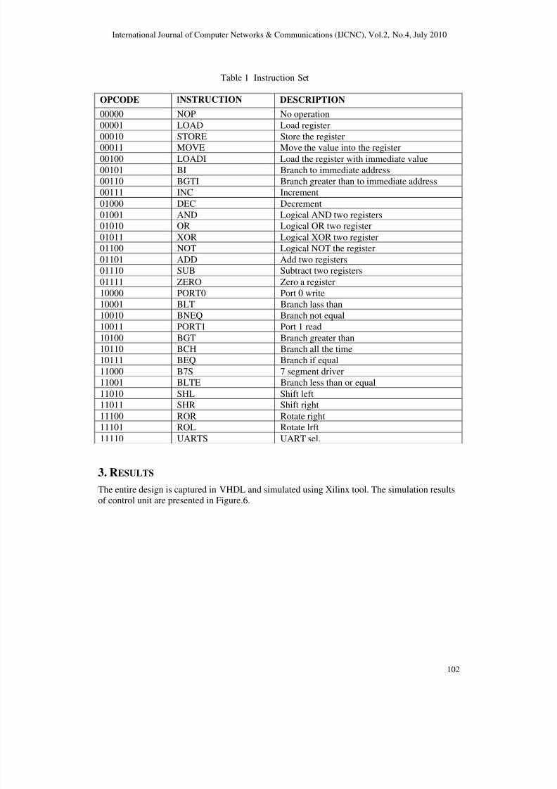
By implementing the instructions given in the instruction set (Table 1) does not cause anyfunctional limitation, but enables an effective way of power saving through generation of gatedclock signals. All the instructions are of length 2 bytes and of direct addressing mode type.Instruction set includes Load, Store, Branch, ALU and Shift instructions.
Control Unit
8/9/2019 POWER OPTIMIZED PROGRAMMABLE EMBEDDED CONTROLLER
http://slidepdf.com/reader/full/power-optimized-programmable-embedded-controller 6/11
International Journal of Computer Networks & Communications (IJCNC), Vol.2, No.4, July 2010
102
Table 1 Instruction Set
OPCODE INSTRUCTION DESCRIPTION
00000 NOP No operation
00001 LOAD Load register
00010 STORE Store the register00011 MOVE Move the value into the register
00100 LOADI Load the register with immediate value00101 BI Branch to immediate address00110 BGTI Branch greater than to immediate address00111 INC Increment
01000 DEC Decrement01001 AND Logical AND two registers01010 OR Logical OR two register
01011 XOR Logical XOR two register01100 NOT Logical NOT the register
01101 ADD Add two registers01110 SUB Subtract two registers
01111 ZERO Zero a register10000 PORT0 Port 0 write10001 BLT Branch lass than10010 BNEQ Branch not equal10011 PORT1 Port 1 read
10100 BGT Branch greater than10110 BCH Branch all the time10111 BEQ Branch if equal
11000 B7S 7 segment driver11001 BLTE Branch less than or equal
11010 SHL Shift left11011 SHR Shift right
11100 ROR Rotate right11101 ROL Rotate lrft
11110 UARTS UART sel.
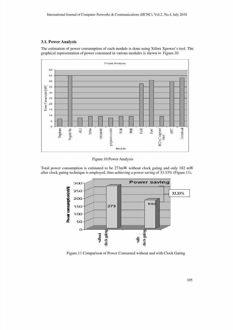
3. RESULTS
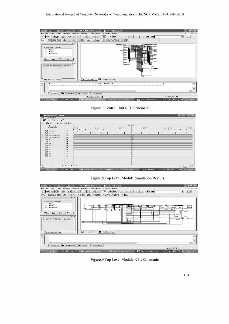
The entire design is captured in VHDL and simulated using Xilinx tool. The simulation resultsof control unit are presented in Figure.6.

8/9/2019 POWER OPTIMIZED PROGRAMMABLE EMBEDDED CONTROLLER
http://slidepdf.com/reader/full/power-optimized-programmable-embedded-controller 7/11
International Journal of Computer Networks & Communications (IJCNC), Vol.2, No.4, July 2010
103
Figure.6 Control Unit Simulation Results
Figure.6 Control Unit Simulation Results (contd…)
Figure.6 Control Unit Simulation Results (contd…)
8/9/2019 POWER OPTIMIZED PROGRAMMABLE EMBEDDED CONTROLLER
http://slidepdf.com/reader/full/power-optimized-programmable-embedded-controller 8/11
International Journal of Computer Networks & Communications (IJCNC), Vol.2, No.4, July 2010
104
Figure.7 Control Unit RTL Schematic
Figure.8 Top Level Module Simulation Results
Figure.9 Top Level Module RTL Schematic
8/9/2019 POWER OPTIMIZED PROGRAMMABLE EMBEDDED CONTROLLER
http://slidepdf.com/reader/full/power-optimized-programmable-embedded-controller 9/11
8/9/2019 POWER OPTIMIZED PROGRAMMABLE EMBEDDED CONTROLLER
http://slidepdf.com/reader/full/power-optimized-programmable-embedded-controller 10/11
International Journal of Computer Networks & Communications (IJCNC), Vol.2, No.4, July 2010
106
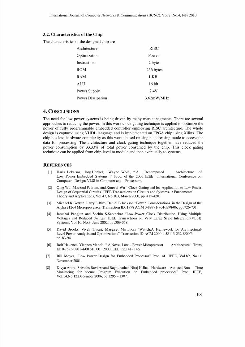
3.2. Characteristics of the Chip
The characteristics of the designed chip are
4. CONCLUSIONS
The need for low power systems is being driven by many market segments. There are severalapproaches to reducing the power. In this work clock gating technique is applied to optimize thepower of fully programmable embedded controller employing RISC architecture. The wholedesign is captured using VHDL language and is implemented on FPGA chip using Xilinx .Thechip has less hardware complexity as this works based on single addressing mode to access thedata for processing. The architecture and clock gating technique together have reduced thepower consumption by 33.33% of total power consumed by the chip. This clock gatingtechnique can be applied from chip level to module and then eventually to systems.
REFERENCES
[1] Haris Lekatsas, Jorg Henkel, Wayne Wolf , “ A Decomposed Architecture of Low Power Embedded Systems ,” Proc. of the 2000 IEEE International Conference on
Computer Design: VLSI in Computer and Processors.[2] Qing Wu, Massoud Pedram, and Xunwei Wu “ Clock-Gating and Its Application to Low Power
Design of Sequential Circuits” IEEE Transactions on Circuits and Systems-1: FundamentalTheory and Applications, Vol.47, No.103, March 2000, pp .415-420.
[3] Michael K.Gowan, Larry L.Biro, Daniel B.Jackson “Power Considerations in the Design of theAlpha 21264 Microprocessor, Transaction ID: 1998 ACM 0-89791-964-5/98/06, pp .726-731
[4] Jatuchai Pangjun and Sachin S.Saptnekar “Low-Power Clock Distribution Using MultipleVoltages and Reduced Swings” IEEE Transactions on Very Large Scale Integration(VLSI)Systems, Vol.10, No.3, June 2002, pp .309-318.
[5] David Brooks, Vivek Tiwari, Margaret Martonosi “Wattch:A Framework for Architectural-Level Power Analysis and Optimizations” Transaction ID:ACM 2000 1-58113-232-8/00/6,pp .83-94.
[6] Rolf Hakenes, Yiannos Manoli, “ A Novel Low – Power Micoprcessor Architecture” Trans.Id: 0-7695-0801-4/00 $10.00 2000 IEEE, pp.141- 146.
[7] Bill Moyer, “Low Power Design for Embedded Processor” Proc. of IEEE, Vol.89, No.11,
November 2001.
[8] Divya Arora, Srivaths Ravi,Anand Raghunathan,Niraj K.Jha, “Hardware – Assisted Run - TimeMonitoring for secure Program Execution on Embedded processors” Proc. IEEE,Vol.14,No.12,December 2006, pp 1295 – 1307.
Architecture RISC
Optimization Power
Instructions 2 byte
ROM 256 bytes
RAM 1 KB
ALU 16 bit
Power Supply 2.4V
Power Dissipation 3.62mW/MHz

8/9/2019 POWER OPTIMIZED PROGRAMMABLE EMBEDDED CONTROLLER
http://slidepdf.com/reader/full/power-optimized-programmable-embedded-controller 11/11
International Journal of Computer Networks & Communications (IJCNC), Vol.2, No.4, July 2010
107
[9] Srikanth Rao and S.K. Nandy , “Power Minimization using Control Generated Clock”,DAC 2000, Los Angeles, California.
[10] Sulaiman, D.R., “Using Clock Gating Technique for Energy Reduction in PortableComputers”, International Conference on Computer and Communication Engineering,ICCCE 2008, 13-15 May 2008, pp.839 - 842 .
[11] Srinivas Devadas, Sharad Malik.A , “ Survey of Optimization Techniques Targeting Low PowerVLSI circuits” , 32nd ACM/IEEE Design Automation Conference.
[12] Brock Barton, Massoud Pedram “Low Power Electronics and Design” IEEE Transactions onVery Large Scale Integration (VLSI) Systems, Vol.5, No.4, December 1997, pp .349-350.
[13] David E.Duarte, N.Vijaykrishnan, and Mary Jane Irwin “A Clock Power Model to EvaluateImpact of Architectural and Technology Optimizations” IEEE Transactions on Very Large ScaleIntegration (VLSI) Systems, Vol.10, No.6, December 2002, pp .844-855.
[14] Monica Donno, Alessandro Ivaldi, Luca Benini, Enrico Macii “Clock-Tree Power Optimizationbased on RTL Clock-Gating”, DAC 2003, pp .622-627.
[15] W.G.Osborne, W.Luk, J.G.F.Coutinho and O.Mencer “Reconfigurable Design with Clock Gating” IEEE Transaction 978-1-4244-1985-2/08, 2008, pp .187-194.
Authors
Dr.K.Lal Kishore , obtained Master’s degree and Ph.D. from Indian Institute of Science (IISC) Bangalore.He had published more than 76 researchpapers in International/Natioanl journals and presented papers inInternational / National Conferences.He is best teacher awardee from theGovernment of Andhrapardesh,S.V.C.Aiya Memorial Award fromIETE,Merit Award from DEC, Ethopia, Bapu Seetharam MemorialAward from IETE and has many other academic distinctions to hiscredit.He wrote books on Electronic Devices,Circuit Analysis,Linear ICApplications,Electronic Measurements and Instrumentation and VLSIDesign.
Dr.A.V.N.Tilak, obtained Master’s degree from Indian Institute of Technology,Kanpur and Ph.D. from Indian Institute of Technology, Madras during1984 and 1997 respectively. He is a Fellow of Institution of ElectronicsAnd Telecommunication Engineers, India and Life Member of IndianSociety for Technical Education.
M.Kamaraju, obtained his Bachelor’s degree & Master’s degree from AndhraUniversity. Areas of interest are Microprocessors, Microcontrollers,Embedded Systems, Low Power VLSI. He is a fellow of Institution of Electronics and Telecommunication Engineers, India & Member of VSI.