Embed Size (px)
Citation preview
LTC4259
14259i
, LTC and LT are registered trademarks of Linear Technology Corporation.
Controls Four Independent –48V PoweredEthernet Ports
Each Channel Includes:– IEEE 802®.3af Compliant PD Detection and
Classification– Inrush Control– Short-Circuit Protection with Current Foldback– PD Disconnect Using AC or DC Sensing– Power Good Indication
Operates Autonomously or Controlled by I2CTM
Serial Interface 4-Bit Programmable Digital Address Allows Control
of Up to 64 Channels Programmable INT Pin Eliminates Software Polling Current Limit Duty Cycle Protects External FETs
Quad IEEE 802.3afPower over Ethernet Controller
with AC DisconnectAugust 2003
IP Phone Systems DTE Power Distribution IEEE 802.3af Compliant Systems
DESCRIPTIO
U
FEATURES
APPLICATIO SU
TYPICAL APPLICATIO
U
Information furnished by Linear Technology Corporation is believed to be accurate and reliable.However, no responsibility is assumed for its use. Linear Technology Corporation makes no represen-tation that the interconnection of its circuits as described herein will not infringe on existing patent rights.
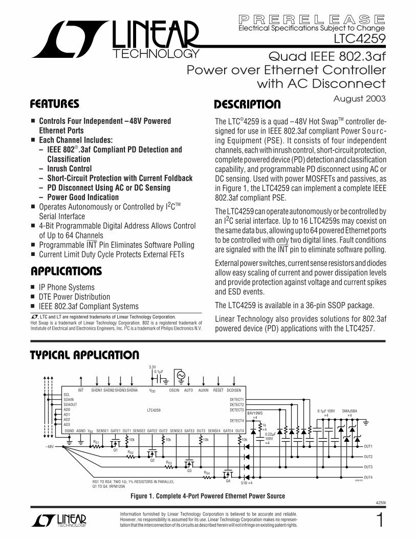
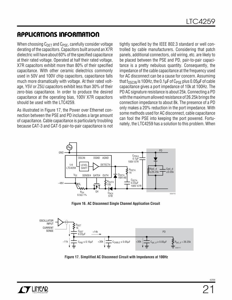
The LTC®4259 is a quad –48V Hot SwapTM controller de-signed for use in IEEE 802.3af compliant Power Sourc-ing Equipment (PSE). It consists of four independentchannels, each with inrush control, short-circuit protection,complete powered device (PD) detection and classificationcapability, and programmable PD disconnect using AC orDC sensing. Used with power MOSFETs and passives, asin Figure 1, the LTC4259 can implement a complete IEEE802.3af compliant PSE.
The LTC4259 can operate autonomously or be controlled byan I2C serial interface. Up to 16 LTC4259s may coexist onthe same data bus, allowing up to 64 powered Ethernet portsto be controlled with only two digital lines. Fault conditionsare signaled with the INT pin to eliminate software polling.
External power switches, current sense resistors and diodesallow easy scaling of current and power dissipation levelsand provide protection against voltage and current spikesand ESD events.
The LTC4259 is available in a 36-pin SSOP package.
Linear Technology also provides solutions for 802.3afpowered device (PD) applications with the LTC4257.
Hot Swap is a trademark of Linear Technology Corporation. 802 is a registered trademark ofInstutute of Electrical and Electronics Engineers, Inc. I2C is a trademark of Philips Electronics N.V.
Figure 1. Complete 4-Port Powered Ethernet Power Source
DGND
AD3
RS1 TO RS4: TWO 1Ω, 1% RESISTORS IN PARALLELQ1 TO Q4: IRFM120A
AD2AD1AD0SDAOUTSDAINSCL
DETECT4
DETECT3
DETECT1DETECT2
AGND
INT
–48V
VEE
SHDN1
SENSE1
RS1
RS2
RS3
RS4
GATE1
Q1
Q2
Q3
Q4 S1B ×4
BAV19WS×4
10k 10k 10k 10k
1k×4
0.22µF100V×4
OUT1
OUT2
OUT3
OUT44259 F01
SMAJ58A×4
0.1µF 100V×4
OUT1 SENSE2 GATE2
LTC4259
OUT2 SENSE3 GATE3 OUT3 SENSE4 GATE4 OUT4
SHDN2 SHDN3 SHDN4 VDD
3.3V0.1µF
AUTOOSCIN AUXIN RESET DCDISEN
Electrical Specifications Subject to Change
LTC4259
24259i
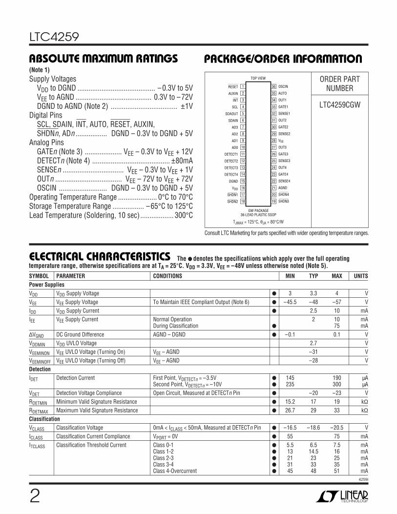
Supply VoltagesVDD to DGND .......................................... –0.3V to 5VVEE to AGND ......................................... 0.3V to –72VDGND to AGND (Note 2) .................................... ±1V
Digital PinsSCL, SDAIN, INT, AUTO, RESET, AUXIN,SHDNn, ADn ................. DGND – 0.3V to DGND + 5V
Analog PinsGATEn (Note 3) .................... VEE – 0.3V to VEE + 12VDETECTn (Note 4) .......................................... ±80mASENSEn ................................. VEE – 0.3V to VEE + 1VOUTn .................................... VEE – 72V to VEE + 72VOSCIN .......................... DGND – 0.3V to DGND + 5V
Operating Temperature Range ..................... 0°C to 70°CStorage Temperature Range ................. –65°C to 125°CLead Temperature (Soldering, 10 sec).................. 300°C
ORDER PARTNUMBER
TJMAX = 125°C, θJA = 80°C/W
LTC4259CGW
(Note 1)ABSOLUTE AXI U RATI GS
W WW U
PACKAGE/ORDER I FOR ATIOU UW
Consult LTC Marketing for parts specified with wider operating temperature ranges.
1
2
3
4
5
6
7
8
9
10
11
12
13
14
15
16
17
18
TOP VIEW
GW PACKAGE36-LEAD PLASTIC SSOP
36
35
34
33
32
31
30
29
28
27
26
25
24
23
22
21
20
19
RESET
AUXIN
INT
SCL
SDAOUT
SDAIN
AD3
AD2
AD1
AD0
DETECT1
DETECT2
DETECT3
DETECT4
DGND
VDD
SHDN1
SHDN2
OSCIN
AUTO
OUT1
GATE1
SENSE1
OUT2
GATE2
SENSE2
VEE
OUT3
GATE3
SENSE3
OUT4
GATE4
SENSE4
AGND
SHDN4
SHDN3
ELECTRICAL CHARACTERISTICS The denotes the specificatiions which apply over the full operatingtemperature range, otherwise specifications are at TA = 25°C. VDD = 3.3V, VEE = –48V unless otherwise noted (Note 5).
SYMBOL PARAMETER CONDITIONS MIN TYP MAX UNITSPower SuppliesVDD VDD Supply Voltage 3 3.3 4 VVEE VEE Supply Voltage To Maintain IEEE Compliant Output (Note 6) –45.5 –48 –57 VIDD VDD Supply Current 2.5 10 mAIEE VEE Supply Current Normal Operation 2 10 mA
During Classification 75 mA∆VGND DC Ground Difference AGND – DGND –0.1 0.1 VVDDMIN VDD UVLO Voltage 2.7 VVEEMINON VEE UVLO Voltage (Turning On) VEE – AGND –31 VVEEMINOFF VEE UVLO Voltage (Turning Off) VEE – AGND –28 VDetectionIDET Detection Current First Point, VDETECTn = –3.5V 145 190 µA
Second Point, VDETECTn = –10V 235 300 µAVDET Detection Voltage Compliance Open Circuit, Measured at DETECTn Pin –20 –23 VRDETMIN Minimum Valid Signature Resistance 15.2 17 19 kΩRDETMAX Maximum Valid Signature Resistance 26.7 29 33 kΩClassificationVCLASS Classification Voltage 0mA < ICLASS < 50mA, Measured at DETECTn Pin –16.5 –18.6 –20.5 VICLASS Classification Current Compliance VPORT = 0V 55 75 mAITCLASS Classification Threshold Current Class 0-1 5.5 6.5 7.5 mA
Class 1-2 13 14.5 16 mAClass 2-3 21 23 25 mAClass 3-4 31 33 35 mAClass 4-Overcurrent 45 48 51 mA
LTC4259
34259i
ELECTRICAL CHARACTERISTICS The denotes the specificatiions which apply over the full operatingtemperature range, otherwise specifications are at TA = 25°C. VDD = 3.3V, VEE = –48V unless otherwise noted (Note 5).
SYMBOL PARAMETER CONDITIONS MIN TYP MAX UNITSGate DriverIGON GATE Pin Current Gate On, VGATEn = VEE –30 –50 –70 µAIGOFF GATE Pin Current Gate Off, VGATEn = VEE + 5V 30 50 80 µAIGPD GATE Pin Short-Circuit Pull-Down VGATEn = VEE + 5V 100 mA∆VGATE External Gate Voltage (VGATEn – VEE) IGATE = –1µA 10 13 15 VOutput Voltage SenseVPG Power Good Threshold Voltage VOUTn – VEE 1 2 3 VIVOUT Out Pin Bias Current 0V > VOUT > –10V –6 µA
–10V > VOUT > –30V –18 µAVOUT = –48V –20 µA
Current SenseVCUT Overcurrent Detection Sense Voltage VSENSEn – VEE, VOUT = VEE 175 187.5 200 mVVLIM Current Limit Sense Voltage VSENSEn – VEE, VOUT = VEE 200 212.5 225 mVVMIN DC Disconnect Sense Voltage VSENSEn – VEE 2.5 3.75 5 mVVSC Short-Circuit Sense Voltage 275 mVISENSE SENSE Pin Bias Current VSENSEn = VEE –40 µAAC Disconnect (Note 7)ROSCIN Input Impedance of OSCIN Pin –0.3V < VSINEIN < 3.3V, fOSC < 200Hz 200 300 kΩAVACD Voltage Gain OSCIN to DETECT1, 2 Channel Powered, PD Not Present –2.7 –3 –3.3 V/V
Voltage Gain OSCIN to DETECT3, 4 Channel Powered, PD Not Present 2.7 3 3.3 V/VIACDMAX AC Disconnect DETECTn Output Current Channel Powered, VDETECTn = ±600 µAIACDMIN Remain Connected DETECTn Current Channel Powered, VDETECTn = 3.4V 150 200 250 µADigital InterfaceVOLD Digital Output Low Voltage SDAOUT, INT, IPIN = 10mA 0.4 VVILD Digital Input Low Voltage SCL, SDAIN 0.8 VVIHD Digital Input High Voltage SCL, SDAIN 2.4 VRPU Pull-Up Resistor to VDD AD0 to AD3, RESET, SHDNn 50 kΩRPD Pull-Down Resistor to DGND AUXIN, AUTO 50 kΩAC CharacteristicstDETDLY Detection Delay From Detect Command or Application of PD to Port 170 590 ms
to Detect Complete (Figure 2)tCLSDLY Classification Delay From Successful Detect in Auto or Semiauto Mode 10.1 52 ms
to Class Complete (Figure 2)From Classify Command in Manual Mode to Class 10.1 420 msComplete
tCLASS Classification Duration (Figure 2) 10.1 13 mstPON Power On Delay, Auto Mode From Valid Detect to Port On in Auto Mode (Figure 2) 90 ms
From Port On Command to GATE Pin Current = IGON 1 mstSTART Maximum Current Limit Duration During tSTART1 = 0, tSTART0 = 0 (Figure 3) 50 60 70 ms
Port Start-Up tSTART1 = 0, tSTART0 = 1 25 30 35 mstSTART1 = 1, tSTART0 = 0 100 120 140 mstSTART1 = 1, tSTART0 = 1 200 240 280 ms
tICUT Maximum Current Limit Duration After tICUT1 = 0, tICUT0 = 0 (Figure 3) 50 60 70 msPort Start-Up tICUT1 = 0, tICUT0 = 1 25 30 35 ms
tICUT1 = 1, tICUT0 = 0 100 120 140 mstICUT1 = 1, tICUT0 = 1 200 240 280 ms
LTC4259
44259i
Note 6: Voltage at the Ethernet connector must be at least –44V forIEEE 802.3af compliance. The minimum VEE supply voltage must takeaccount for the drop across the diode DAC in Figure 15.Note 7: Unless otherwise specified, AC disconnect specifications requirethe following conditions: the DETECTn pin is connected to the port asshown in Figure 1, a valid sine wave is applied to OSCIN, the OSCFAIL bitis cleared and AC disconnect is enabled.Note 8: Guaranteed by design, not subject to test.Note 9: Values measured at VILD and VIHD.Note 10: If fault occurs during an I2C transaction, INT pin will not be pulleddown until a stop condition is present on the I2C bus.
Note 1: Absolute Maximum Ratings are those values beyond which the lifeof the device may be impaired.Note 2: DGND to AGND voltages beyond ±100mV will prevent properoperation of the classification function.Note 3: An internal clamp limits the GATE pins to a minimum of 12V aboveVEE. Driving this pin beyond the clamp may damage the part.Note 4: When a port powers on or off, the transient voltage on the portcouples through CDET (Figure 15). The LTC4259 contains internalprotection circuitry to withstand transient currents of up to 80mA for 5ms.As long as the absolute value of the current remains below 80mA, theLTC4259 will keep the voltage at the DETECTn pin within the absolutemaximum voltage range. A properly sized RDET will limit the current to lessthan 60mA.Note 5: All currents into device pins are positive; all currents out of devicepins are negative. All voltages are referenced to ground (AGND and DGND)unless otherwise specified.
ELECTRICAL CHARACTERISTICS The denotes the specificatiions which apply over the full operatingtemperature range, otherwise specifications are at TA = 25°C. VDD = 3.3V, VEE = –48V unless otherwise noted (Note 5).
SYMBOL PARAMETER CONDITIONS MIN TYP MAX UNITSDCCLMAX Maximum Current Limit Duty Cycle 5.8 6.3 6.7 %tDIS Disconnect Delay tDIS1 = 0, tDIS0 = 0 (Figures 4, 5) 300 360 400 ms
tDIS1 = 0, tDIS0 = 1 75 90 100 mstDIS1 = 1, tDIS0 = 0 150 180 200 mstDIS1 = 1, tDIS0 = 1 600 720 800 ms
tVMIN DC Disconnect Minimum Pulse VSENSEn – VEE > 5mV, VOUTn = –48V (Figure 4) 0.02 1 msWidth Sensitivity
I2C TimingfSCLK Clock Frequency (Note 8) 400 kHzt1 Bus Free Time Figure 6 (Notes 8, 9) 1.3 µst2 Start Hold Time Figure 6 (Notes 8, 9) 600 nst3 SCL Low Time Figure 6 (Notes 8, 9) 1.3 µst4 SCL High Time Figure 6 (Notes 8, 9) 600 nst5 Data Hold Time Figure 6 (Notes 8, 9) 150 nst6 Data Set-Up Time Figure 6 (Notes 8, 9) 200 nst7 Start Set-Up Time Figure 6 (Notes 8, 9) 600 nst8 Stop Set-Up Time Figure 6 (Notes 8, 9) 600 nstr SCL, SDAIN Rise Time Figure 6 (Notes 8, 9) 20 300 nstf SCL, SDAIN Fall Time Figure 6 (Notes 8, 9) 20 150 nstFLTINT Fault Present to INT Pin Low (Notes 8, 9, 10) 20 150 nstSTOPINT Stop Condition to INT Pin Low (Notes 8, 9, 10) 60 200 nstARAINT ARA to INT Pin High Time (Notes 8, 9) 20 300 ns
LTC4259
54259i
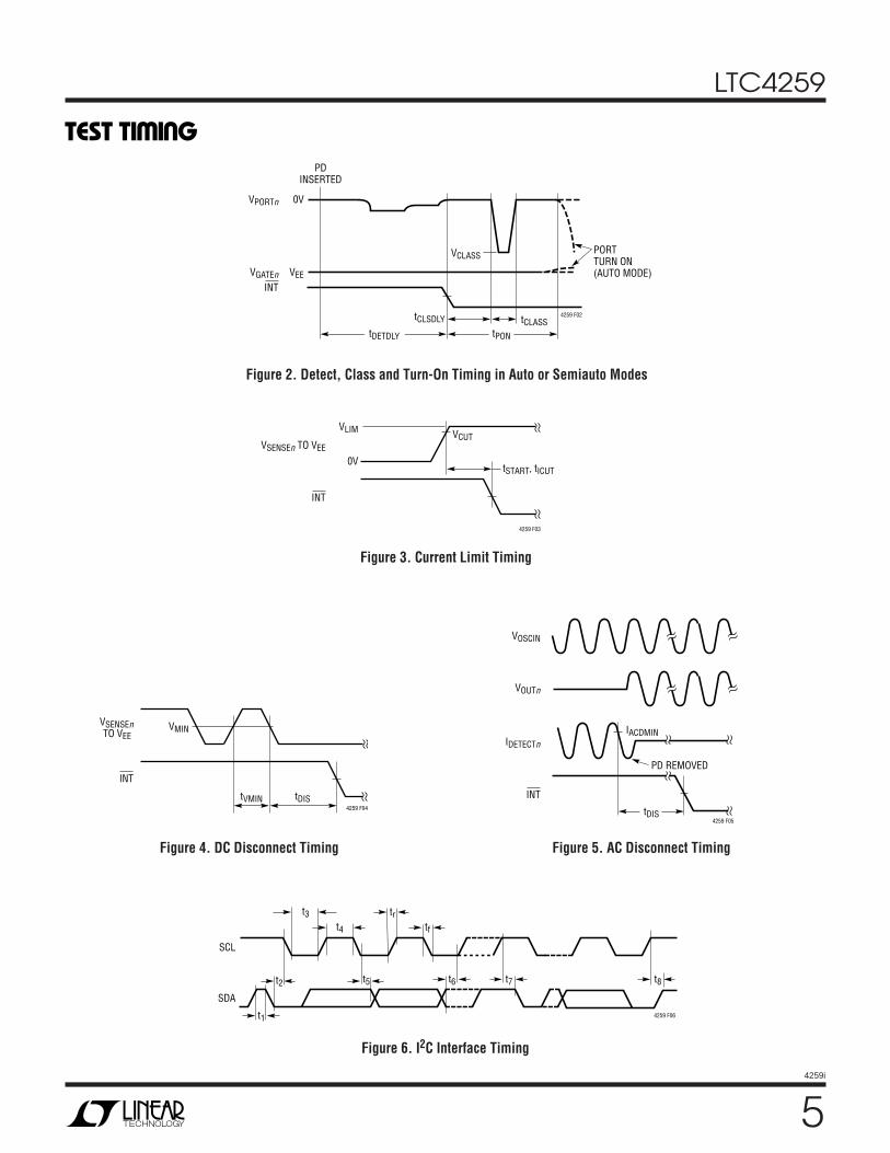
Figure 3. Current Limit Timing
Figure 4. DC Disconnect Timing Figure 5. AC Disconnect Timing
TEST TI I G
WUFigure 6. I2C Interface Timing
Figure 2. Detect, Class and Turn-On Timing in Auto or Semiauto Modes
SCL
SDA
t1
t2
t3 trtf
t5 t6 t7 t8
t4
4259 F06
0VVPORTn
VGATEnINT
PDINSERTED
VEE
VCLASS PORT TURN ON (AUTO MODE)
tCLSDLY tCLASS4259 F02
tDETDLY tPON
VLIM VCUT
0V
VSENSEn TO VEE
INT
4259 F03
tSTART, tICUT
VMINVSENSEnTO VEE
INT
tDIStVMIN4259 F04
INT
IDETECTn
VOUTn
VOSCIN
tDIS
IACDMIN
PD REMOVED
4259 F05
LTC4259
64259i
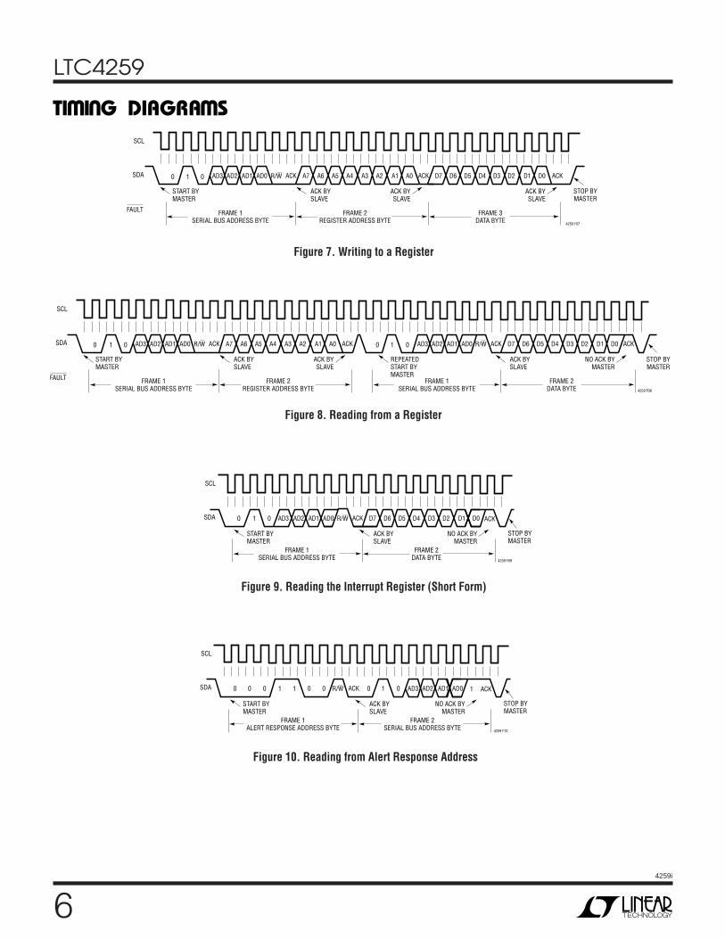
Figure 9. Reading the Interrupt Register (Short Form)
Figure 7. Writing to a Register
Figure 8. Reading from a Register
Figure 10. Reading from Alert Response Address
TI I G DIAGRA S
WU W
SCL
SDA
4259 F07
0 01 AD3 AD2 AD1 AD0 A7 A6 A5 A4 A3 A2 A1 A0R/W ACK D7 D6 D5 D4 D3 D2 D1 D0ACK ACK
START BYMASTER
ACK BYSLAVE
ACK BYSLAVE
ACK BYSLAVE
FRAME 1SERIAL BUS ADDRESS BYTE
FRAME 2REGISTER ADDRESS BYTE
FRAME 3DATA BYTE
STOP BYMASTER
FAULT
SCL
SDA 0 01 AD3 AD2 AD1 AD0 A7 A6 A5 A4 A3 A2 A1 A0R/W ACK ACK 0 01 AD3 AD2 AD1 AD0 D7 D6 D5 D4 D3 D2 D1 D0R/W ACK ACK
START BYMASTER
ACK BYSLAVE
ACK BYSLAVE
4259 F08
STOP BYMASTER
REPEATEDSTART BYMASTER
ACK BYSLAVE
NO ACK BYMASTER
FRAME 1SERIAL BUS ADDRESS BYTE
FRAME 2REGISTER ADDRESS BYTE
FRAME 1SERIAL BUS ADDRESS BYTE
FRAME 2DATA BYTE
FAULT
SCL
SDA
4259 F09
0 1 0 AD3 AD2 AD1 AD0 D7 D6 D5 D4 D3 D2 D1 D0R/W ACK ACK
START BYMASTER
ACK BYSLAVE
NO ACK BYMASTER
FRAME 1SERIAL BUS ADDRESS BYTE
FRAME 2DATA BYTE
STOP BYMASTER
SCL
SDA
4259 F10
0 0 110 AD30000 1 AD2 AD1 AD0R/W ACK ACK1
START BYMASTER
ACK BYSLAVE
NO ACK BYMASTER
FRAME 1ALERT RESPONSE ADDRESS BYTE
FRAME 2SERIAL BUS ADDRESS BYTE
STOP BYMASTER
LTC4259
74259i
UUU
PI FU CTIO SRESET (Pin 1): Chip Reset, Active Low. When the RESETpin is low, the LTC4259 is held inactive with all channelsoff and all internal registers reset to their power-up states.When RESET is pulled high, the LTC4259 begins normaloperation. RESET can be connected to an external capaci-tor or RC network to provide a power turn-on delay. Aninternal 50k resistor pulls RESET high if not externallypulled down. Internal filtering of the RESET pin preventsglitches less than 1µs from resetting the LTC4259.
AUXIN (Pin 2): Auxiliary Input. The real time state of theAUXIN pin can be read at bit 1 in the Pin Status register(11h). An internal 50k resistor pulls AUXIN low if it is leftfloating. The AUXIN pin provides a simple way for the hostcontroller to read the state of a switch or other humaninterface device.
INT (Pin 3): Interrupt Output, Open Drain. INT will pull lowwhen any one of several events occur in the LTC4259. Itwill return to a high impedance state when bits 6 or 7 areset in the Reset PB register (1Ah). The INT signal can beused to generate an interrupt to the host processor,eliminating the need for continuous software polling.Individual INT events can be disabled using the Int Maskregister (01h). See Register Functions and ApplicationsInformation for more information. The INT pin is onlyupdated between I2C transactions.
SCL (Pin 4): Serial Clock Input. High impedance clockinput for the I2C serial interface bus. The SCL pin shouldbe connected directly to the I2C SCL bus line.
SDAOUT (Pin 5): Serial Data Output, Open Drain DataOutput for the I2C Serial Interface Bus. The LTC4259 usestwo pins to implement the bidirectional SDA function tosimplify optoisolation of the I2C bus. To implement a stan-dard bidirectional SDA pin, tie SDAOUT and SDAIN to-gether. See Applications Information for more information.
SDAIN (Pin 6): Serial Data Input. High impedance data inputfor the I2C serial interface bus. The LTC4259 uses two pinsto implement the bidirectional SDA function to simplifyoptoisolation of the I2C bus. To implement a standardbidirectional SDA pin, tie SDAOUT and SDAIN together.See Applications Information for more information.
AD3 (Pin 7): Address Bit 3. Tie the address pins high or lowto set the I2C serial address to which LTC4259 responds.This address will be (010A3A2A1A0)b. An internal 50kresistor pulls AD3 high if it is left floating.
AD2 (Pin 8): Address Bit 2. See AD3.
AD1 (Pin 9): Address Bit 1. See AD3.
AD0 (Pin 10): Address Bit 0. See AD3.
DETECT1 (Pin 11): Detection Sense, Channel 1. TheLTC4259 powered device (PD) detection and AC discon-nect hardware monitors port 1 with this pin. ConnectDETECT1 to the port 1 output via a 100V 75mA signaldiode in parallel with a 0.2µF 100V X7R capacitor in serieswith a 1k resistor (see Figure 1). The resistor and capacitormay be eliminated if AC disconnect is not used.
DETECT2 (Pin 12): Detection Sense, Channel 2. SeeDETECT1.
DETECT3 (Pin 13): Detection Sense, Channel 3. SeeDETECT1.
DETECT4 (Pin 14): Detection Sense, Channel 4. SeeDETECT1.
DGND (Pin 15): Digital Ground. DGND should be con-nected to the return from the 3.3V supply. DGND andAGND should typically be tied together. However, DGNDcan be separated from AGND by as musch as ±100mV andremain IEEE compliant.
VDD (Pin 16): Logic Power Supply. Connect to a 3.3Vpower supply relative to DGND. VDD must be bypassed toDGND near the LTC4259 with at least a 0.1µF capacitor.
SHDN1 (Pin 17): Shutdown Channel 1, Active Low. Whenpulled low, SHDN1 shuts down channel 1, regardless ofthe state of the internal registers. Pulling SHDN1 low isequivalent to setting the Reset Port 1 bit in the ResetPushbutton register (1Ah). An internal 50k resistor pullsSHDN1 high if it is left floating and an internal filter with atime constant greater than 1µs prevents glitches fromshutting down the port.
LTC4259
84259i
UUU
PI FU CTIO SSHDN2 (Pin 18): Shutdown Channel 2, Active Low. SeeSHDN1.
SHDN3 (Pin 19): Shutdown Channel 3, Active Low. SeeSHDN1.
SHDN4 (Pin 20): Shutdown Channel 4, Active Low. SeeSHDN1.
AGND (Pin 21): Analog Ground. AGND should be con-nected to the return from the –48V supply. AGND andDGND should typically be tied together. However, if theyare not, AGND can be separated from DGND by no morethan ±100mV.
SENSE4 (Pin 22): Channel 4 Current Sense Input. SENSE4monitors the external MOSFET current via a 0.5Ω senseresistor between SENSE4 and VEE. Whenever the voltageacross the sense resistor exceeds the overcurrent detec-tion threshold VCUT, the current limit fault timer counts up.If the voltage across the sense resistor reaches the currentlimit threshold VLIM (typically 25mV/50mA higher), theGATE4 pin voltage is lowered to maintain constant currentin the external MOSFET. See Applications Information forfurther details. If the channel is unused, the SENSE4 pinmust be tied to VEE.
GATE4 (Pin 23): Channel 4 Gate Drive. GATE4 should beconnected to the gate of the external channel 4 MOSFET.When the MOSFET is turned on, a 50µA pull-up currentsource is connected to the pin. The gate voltage is clampedto 13V (typ) above VEE. During a current limit condition,the voltage at GATE4 will be reduced to maintain constantcurrent through the external MOSFET. If the fault timerexpires, GATE4 is pulled down with 50µA, turning theMOSFET off and recording a tICUT or tSTART event. If thechannel is unused, float the GATE4 pin or tie it to VEE.
OUT4 (Pin 24): Channel 4 Output Voltage Monitor. OUT4should be connected to the output port through a 10kseries resistor. A current limit foldback circuit limits thepower dissipation in the external MOSFET by reducing thecurrent limit threshold when the output voltage is within18V of AGND. The port 4 Power Good bit is set when thevoltage from OUT4 to VEE drops below 2V (typ). A 2.5MΩresistor is connected internally from OUT4 to AGND. If the
channel is unused, the OUT4 pin can be tied to AGND orallowed to float.
SENSE3 (Pin 25): Channel 3 Current Sense Input. SeeSENSE4.
GATE3 (Pin 26): Channel 3 Gate Drive. See GATE4.
OUT3 (Pin 27): Channel 3 Output Voltage Monitor. SeeOUT4.
VEE (Pin 28): – 48V Supply Input. Connect to a –45.5V to–57V supply, relative to AGND.
SENSE2 (Pin 29): Channel 2 Current Sense Input. SeeSENSE4.
GATE2 (Pin 30): Channel 2 Gate Drive. See GATE4.
OUT2 (Pin 31): Channel 2 Output Voltage Monitor. SeeOUT4.
SENSE1 (Pin 32): Channel 1 Current Sense Input. SeeSENSE4.
GATE1 (Pin 33): Channel 1 Gate Drive. See GATE 4.
OUT1 (Pin 34): Channel 1 Output Voltage Monitor. SeeOUT4.
AUTO (Pin 35): Auto Mode Input. Auto mode is intendedto allow the LTC4259 to detect and power up a PD even ifthere is no host controller present on the I2C bus. Whenthis pin is high, all Mode bits in the Operating Moderegister will be set at power-up or after a system reset.When this pin is low, all Mode bits will be cleared atpower-up or after a system reset. The states of the Modebits can be subsequently changed via the I2C interface ifdesired. The real-time state of the AUTO pin can be readat bit 0 in the Pin Status register (11h). An internal 50kresistor pulls AUTO low if it is left floating.
OSCIN (Pin 36): Oscillator Input. Connect to an oscillatingsignal source, preferably a sine wave, of approximately100Hz with 2V peak-to-peak amplitude, negative peaksabove – 0.3V and positive peaks below 2.5V. When achannel is powered and AC disconnect is enabled, thissignal is used to detect the AC impedance of the PD.
LTC4259
94259i
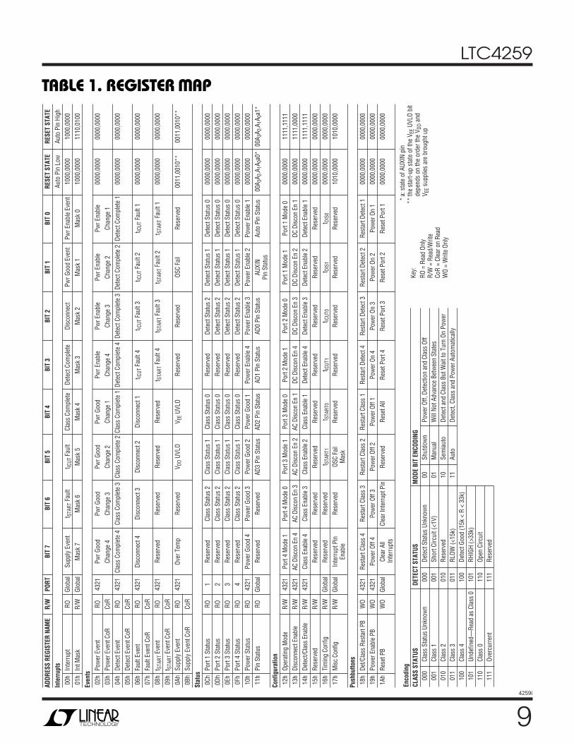
TABLE 1. REGISTER AP
W
*a:
sta
te o
f AUX
IN p
in**
the
star
t-up
stat
e of
the
V EE
UVLO
bit
depe
nds
on th
e or
der t
he V
DD a
ndV E
E sup
plie
s ar
e br
ough
t up
Enco
ding
CLAS
S ST
ATUS
DETE
CT S
TATU
SM
ODE
BIT
ENCO
DING
000
Clas
s St
atus
Unk
now
n00
0De
tect
Sta
tus
Unkn
own
00Sh
utdo
wn
Pow
er O
ff, D
etec
tion
and
Clas
s Of
f00
1Cl
ass
100
1Sh
ort C
ircui
t (<1
V)01
Man
ual
Will
Not
Adv
ance
Bet
wee
n St
ates
010
Clas
s 2
010
Rese
rved
10Se
mia
uto
Dete
ct a
nd C
lass
But
Wai
t to
Turn
On
Pow
er01
1Cl
ass
301
1RL
OW (<
15k)
11Au
toDe
tect
, Cla
ss a
nd P
ower
Aut
omat
ical
ly10
0Cl
ass
410
0De
tect
Goo
d (1
5k <
R <
33k
)10
1Un
defin
ed—
Read
as
Clas
s 0
101
RHIG
H (>
33k)
110
Clas
s 0
110
Open
Circ
uit
111
Over
curr
ent
111
Rese
rved
ADDR
ESS
REGI
STER
NAM
ER/
WPO
RTBI
T 7
BIT
6BI
T 5
BIT
4BI
T 3
BIT
2BI
T 1
BIT
0RE
SET
STAT
ERE
SET
STAT
EIn
terr
upts
Auto
Pin
Low
Auto
Pin
Hig
h00
hIn
terr
upt
ROGl
obal
Supp
ly E
vent
t STA
RT F
ault
t ICUT
Fau
ltCl
ass
Com
plet
eDe
tect
Com
plet
eDi
scon
nect
Pwr G
ood
Even
tPw
r Ena
ble
Even
t10
00,0
000
1000
,000
001
hIn
t Mas
kR/
WGl
obal
Mas
k 7
Mas
k 6
Mas
k 5
Mas
k 4
Mas
k 3
Mas
k 2
Mas
k 1
Mas
k 0
1000
,000
011
10,0
100
Even
ts02
hPo
wer
Eve
ntRO
4321
Pwr G
ood
Pwr G
ood
Pwr G
ood
Pwr G
ood
Pwr E
nabl
ePw
r Ena
ble
Pwr E
nabl
ePw
r Ena
ble
0000
,000
000
00,0
000
03h
Pow
er E
vent
CoR
CoR
Chan
ge 4
Chan
ge 3
Chan
ge 2
Chan
ge 1
Chan
ge 4
Chan
ge 3
Chan
ge 2
Chan
ge 1
04h
Dete
ct E
vent
RO43
21Cl
ass
Com
plet
e 4
Clas
s Co
mpl
ete
3Cl
ass
Com
plet
e 2
Clas
s Co
mpl
ete
1De
tect
Com
plet
e 4
Dete
ct C
ompl
ete
3De
tect
Com
plet
e 2
Dete
ct C
ompl
ete
100
00,0
000
0000
,000
005
hDe
tect
Eve
nt C
oRCo
R06
hFa
ult E
vent
RO43
21Di
scon
nect
4Di
scon
nect
3Di
scon
nect
2Di
scon
nect
1t IC
UT F
ault
4t IC
UT F
ault
3t IC
UT F
ault
2t IC
UT F
ault
100
00,0
000
0000
,000
007
hFa
ult E
vent
CoR
CoR
08h
t STA
RT E
vent
RO43
21Re
serv
edRe
serv
edRe
serv
edRe
serv
edt S
TART
Fau
lt 4
t STA
RT F
ault
3t S
TART
Fau
lt 2
t STA
RT F
ault
100
00,0
000
0000
,000
009
ht S
TART
Eve
nt C
oRCo
R0A
hSu
pply
Eve
ntRO
4321
Over
Tem
pRe
serv
edV D
D UV
LOV E
E UVL
ORe
serv
edRe
serv
edOS
C Fa
ilRe
serv
ed00
11,0
010*
*00
11,0
010*
*0B
hSu
pply
Eve
nt C
oRCo
RSt
atus
0Ch
Port
1 St
atus
RO1
Rese
rved
Clas
s St
atus
2Cl
ass
Stat
us 1
Clas
s St
atus
0Re
serv
edDe
tect
Sta
tus
2De
tect
Sta
tus
1De
tect
Sta
tus
000
00,0
000
0000
,000
00D
hPo
rt 2
Stat
usRO
2Re
serv
edCl
ass
Stat
us 2
Clas
s St
atus
1Cl
ass
Stat
us 0
Rese
rved
Dete
ct S
tatu
s 2
Dete
ct S
tatu
s 1
Dete
ct S
tatu
s 0
0000
,000
000
00,0
000
0Eh
Port
3 St
atus
RO3
Rese
rved
Clas
s St
atus
2Cl
ass
Stat
us 1
Clas
s St
atus
0Re
serv
edDe
tect
Sta
tus
2De
tect
Sta
tus
1De
tect
Sta
tus
000
00,0
000
0000
,000
00F
hPo
rt 4
Stat
usRO
4Re
serv
edCl
ass
Stat
us 2
Clas
s St
atus
1Cl
ass
Stat
us 0
Rese
rved
Dete
ct S
tatu
s 2
Dete
ct S
tatu
s 1
Dete
ct S
tatu
s 0
0000
,000
000
00,0
000
10h
Pow
er S
tatu
sRO
4321
Pow
er G
ood
4Po
wer
Goo
d 3
Pow
er G
ood
2Po
wer
Goo
d 1
Pow
er E
nabl
e 4
Pow
er E
nabl
e 3
Pow
er E
nabl
e 2
Pow
er E
nabl
e 1
0000
,000
000
00,0
000
11h
Pin
Stat
usRO
Glob
alRe
serv
edRe
serv
edAD
3 Pi
n St
atus
AD2
Pin
Stat
usAD
1 Pi
n St
atus
AD0
Pin
Stat
usAU
XIN
Auto
Pin
Sta
tus
00A 3
A 2,A
1A0a
0*00
A 3A 2
,A1A
0a1*
Pin
Stat
usCo
nfig
urat
ion
12h
Oper
atin
g M
ode
R/W
4321
Port
4 M
ode
1Po
rt 4
Mod
e 0
Port
3 M
ode
1Po
rt 3
Mod
e 0
Port
2 M
ode
1Po
rt 2
Mod
e 0
Port
1 M
ode
1Po
rt 1
Mod
e 0
0000
,000
011
11,1
111
13h
Disc
onne
ct E
nabl
eR/
W43
21AC
Dis
con
En 4
AC D
isco
n En
3AC
Dis
con
En 2
AC D
isco
n En
1DC
Dis
con
En 4
DC D
isco
n En
3DC
Dis
con
En 2
DC D
isco
n En
100
00,0
000
1111
,000
014
hDe
tect
/Cla
ss E
nabl
eR/
W43
21Cl
ass
Enab
le 4
Clas
s En
able
3Cl
ass
Enab
le 2
Clas
s En
able
1De
tect
Ena
ble
4De
tect
Ena
ble
3De
tect
Ena
ble
2De
tect
Ena
ble
100
00,0
000
1111
,111
115
hRe
serv
edR/
WRe
serv
edRe
serv
edRe
serv
edRe
serv
edRe
serv
edRe
serv
edRe
serv
edRe
serv
ed00
00,0
000
0000
,000
016
hTi
min
g Co
nfig
R/W
Glob
alRe
serv
edRe
serv
edt S
TART
1t S
TART
0t IC
UT1
t ICUT
0t D
IS1
t DIS
000
00,0
000
0000
,000
017
hM
isc
Conf
igR/
WGl
obal
Inte
rrup
t Pin
Rese
rved
OSC
Fail
Rese
rved
Rese
rved
Rese
rved
Rese
rved
Rese
rved
1010
,000
010
10,0
000
Enab
leM
ask
Push
butto
ns18
hDe
t/Cla
ss R
esta
rt PB
WO
4321
Rest
art C
lass
4Re
star
t Cla
ss 3
Rest
art C
lass
2Re
star
t Cla
ss 1
Rest
art D
etec
t 4Re
star
t Det
ect 3
Rest
art D
etec
t 2Re
star
t Det
ect 1
0000
,000
000
00,0
000
19h
Pow
er E
nabl
e PB
WO
4321
Pow
er O
ff 4
Pow
er O
ff 3
Pow
er O
ff 2
Pow
er O
ff 1
Pow
er O
n 4
Pow
er O
n 3
Pow
er O
n 2
Pow
er O
n 1
0000
,000
000
00,0
000
1Ah
Rese
t PB
WO
Glob
alCl
ear A
llCl
ear I
nter
rupt
Pin
Rese
rved
Rese
t All
Rese
t Por
t 4Re
set P
ort 3
Rese
t Por
t 2Re
set P
ort 1
0000
,000
000
00,0
000
Inte
rrup
ts
Key:
RO =
Rea
d On
lyR/
W =
Rea
d/W
rite
CoR
= Cl
ear o
n Re
adW
O =
Writ
e On
ly
LTC4259
104259i
Interrupt Registers
Interrupt (Address 00h): Interrupt Register, Read Only. Atransition to logical 1 of any bit in this register will assertthe INT pin (Pin 3) if the corresponding bit in the Int Maskregister is set. Each bit is the logical OR of the correspond-ing bits in the Event registers. The Interrupt register is ReadOnly and its bits cannot be cleared directly. To clear a bitin the Interrupt register, clear the corresponding bits in theappropriate Status or Event registers.
Int Mask (Address 01h): Interrupt Mask, Read/Write. A logic1 in any bit of the Int Mask register allows the correspond-ing Interrupt register bit to assert the INT pin if it is set. Alogic 0 in any bit of the Int Mask register prevents thecorresponding Interrupt bit from affecting the INT pin. Theactual Interrupt register bits are unaffected by the state ofthe Int Mask register.
Event Registers
Power Event (Address 02h): Power Event Register, ReadOnly. The lower four bits in this register indicate that thecorresponding port Power Enable status bit has changed;the logical OR of these four bits appears in the Interruptregister as the Pwr Enable Event bit. The upper four bitsindicate that the corresponding port Power Good status bithas changed; the logical OR of these four bits appears inthe Interrupt register as the Pwr Good Event bit. The PowerEvent bits latch high and will remain high until cleared byreading from address 03h.
Power Event CoR (Address 03h): Power Event Register,Clear on Read. Read this address to clear the Power Eventregister. Address 03h returns the same data as address 02hand reading address 03h clears all bits at both addresses.
Detect Event (Address 04h): Detect Event Register, ReadOnly. The lower four bits in this register indicate that at leastone detection cycle for the corresponding port has com-pleted; the logical OR of these four bits appears in theInterrupt register as the Detect Complete bit. The upper fourbits indicate that at least one classification cycle for thecorresponding port has completed; the logical OR of thesefour bits appears in the Interrupt register as the ClassComplete bit. In Manual mode, this register indicates thatthe requested detection/classification cycle has completedand the LTC4259 is awaiting further instructions. In
REGISTER FU CTIO S
U U
Semiauto or Auto modes, these bits indicate that the De-tect Status and Class Status bits in the Port Status regis-ters are valid. The Detect Event bits latch high and will remainhigh until cleared by reading from address 05h.
Detect Event CoR (Address 05h): Detect Event Register,Clear on Read. Read this address to clear the Detect Eventregister. Address 05h returns the same data as address 04h,and reading address 05h clears all bits at both addresses.
Fault Event (Address 06h): Fault Event Register, Read Only.The lower four bits in this register indicate that atICUT fault has occurred at the corresponding port; the logi-cal OR of these four bits appears in the Interrupt register asthe tICUT Fault bit. The upper four bits indicate that a Discon-nect event has occurred at the corresponding port; the logi-cal OR of these four bits appears in the Interrupt register asthe Disconnect bit. The Fault Event bits latch high and willremain high until cleared by reading from address 07h.
Fault Event CoR (Address 07h): Fault Event Register, Clearon Read. Read this address to clear the Fault Event regis-ter. Address 07h returns the same data as address 06h andreading address 07h clears all bits at both addresses.
tSTART Event (Address 08h): tSTART Event Register, ReadOnly. The lower four bits in this register indicate that a tSTARTfault has occurred at the corresponding port; the logical ORof these four bits appears in the Interrupt register as thetSTART Fault bit. The tSTART Event bits latch high and willremain high until cleared by reading from address 09h. Theupper four bits in this register are reserved and will alwaysread as 0.
tSTART Event CoR (Address 09h): tSTART Event Register,Clear on Read. Read this address to clear the Fault Eventregister. Address 09h returns the same data as address 08hand reading address 09h clears all bits at both addresses.
Supply Event (Address 0Ah): Supply Event Register, ReadOnly. Bit 1, Osc Fail, sets when the signal at Pin 36, OSCIN,is absent or does not have the required amplitude and ACdisconnect cannot operate properly. The Osc Fail bit latcheshigh and will remain high until cleared by reading at 0Bh.The Osc Fail bit is set after power on or reset. Power is re-moved on ports with AC disconnect enabled independentlyof the state of the Osc Fail bit. See AC Disconnect underApplications Information for more details. Bit 4 indicatesthat VEE has dropped below the VEE UVLO level (typically
LTC4259
114259i
–26V). Bit 5 signals that the VDD supply has dropped be-low the VDD UVLO threshold. Bit 7 indicates that theLTC4259 die temperature has exceeded its thermal shut-down (TSD) limit. Thermal shutdown is intended to protectagainst momentary overload conditions. Junction tempera-ture will exceed 125°C while in thermal shutdown.Continous operation above the specified maximum oper-ating temperature may result in device degredation or fail-ure. The logical OR of bits 1, 4, 5 and 7 appears in theInterrupt register as the Supply Fault bit. See the Misc Configregister for information on masking the Osc Fail bit out ofthe Supply Fault interrupt. The remaining bits in the regis-ter are reserved and will always read as 0. The Supply Eventbits latch high and will remain high until cleared by readingfrom address 0Bh.
Supply Event CoR (Address 0Bh): Supply Event Register,Clear on Read. Read this address to clear the Fault Eventregister. Address 0Bh returns the same data as address 0Ah,and reading address 0Bh clears all bits at both addresses.
Status Registers
Port 1 Status (Address 0Ch): Port 1 Status Register, ReadOnly. This register reports the most recent detection andclassification results for port 1. Bits 0-2 report the statusof the most recent detection attempt at the port and bits 4-6report the status of the most recent classification attemptat the port. If power is on, these bits report the detection/classification status present just before power was turnedon. If power is turned off at the port for any reason, all bitsin this register will be cleared. See Table 1 for detection andclassification status bit encoding.
Port 2 Status (Address 0Dh): Port 2 Status Register, ReadOnly. See Port 1 Status.
Port 3 Status (Address 0Eh): Port 3 Status Register, ReadOnly. See Port 1 Status.
Port 4 Status (Address 0Fh): Port 4 Status Register, ReadOnly. See Port 1 Status.
Power Status (Address 10h): Power Status Register, ReadOnly. The lower four bits in this register report the switchon/off state for the corresponding ports. The upper fourbits, the power good bits, indicate that the drop across thepower switch and sense resistor for the corresponding portsis less than 2V, indicating that power start-up is complete
and no current faults are present. The power good bits arelatched high and are only cleared when a port is turned offor the LTC4259 is reset.Pin Status (Address 11h): External Pin Status, Read Only.This register reports the real time status of the externalAUTO (Pin 35), AUXIN (Pin 2), and AD0-AD3 (Pins 7-10).The logic state of the AUTO pin appears at bit 0, the AUXINpin at bit 1, and the AD0-AD3 pins at bits 2-5. The remain-ing bits are reserved and will read as 0. AUTO affects theinitial states of some of the LTC4259 configuration regis-ters at start-up but has no effect after start-up and can beused as a general purpose input if desired, as long as it isguaranteed to be in the appropriate state at start-up.
Configuration Registers
Operating Mode (Address 12h): Operating Mode Configu-ration, Read/Write. This register contains the mode bits foreach of the four ports in the LTC4259. See Table 1 for modebit encoding. At power-up, all bits in this register will be setto the logic state of the AUTO pin (Pin 35). See OperatingModes in the Applications Information section.
Disconnect Enable (Address 13h): Disconnect EnableRegister, Read/Write. The lower four bits of this registerenable or disable DC disconnect detection circuitry at thecorresponding port. If the DC Discon Enable bit is set theport circuitry will turn off power if the current draw at theport falls below IMIN for more than tDIS. IMIN is equal to VMIN/RS, where RS is the sense resistor and should be 0.5Ω forIEEE 802.3af compliance. If the bit is clear the port will notremove power due to low current.
The upper four bits enable or disable AC disconnect on thecorresponding port. When a port’s AC disconnect bit is set,the LTC4259 senses the impedance of that port by forcingan AC voltage on the port’s DETECT pin and measuring theAC current. If the DETECT pin sinks less than IACDMIN formore than tDIS, the port will turn off power. If the bit is clear,the port will not remove power due to high port impedance(AC current below IACDMIN).The DC and AC disconnect signals are ORed together andeither sensing method (if they are both enabled) will keepthe port powered. A port with neither DC or AC disconnectenabled will not power off automatically when the PD isremoved.
REGISTER FU CTIO S
U U
LTC4259
124259i
Det/Class Restart PB (Address 18h): Detection/Classifi-cation Restart Pushbutton Register, Write Only. Writing a1 to any bit in this register will start or restart a singledetection or classification cycle at the corresponding portin Manual mode. It can also be used to set the correspond-ing bits in the Detect/Class Enable register (address 14h)for ports in auto or semiauto mode. The lower 4 bits affectdetection on each port while the upper 4 bits affectclassification.
Power Enable PB (Address 19h): Power Enable PushbuttonRegister, Write Only. The lower four bits of this register setthe Power Enable bit in the corresponding Port Statusregister; the upper four bits clear the corresponding PowerEnable bit. Setting or clearing the Power Enable bits via thisregister will turn on or off the power in any mode exceptshutdown, regardless of the state of detection or classifi-cation. Note that tICUT, tSTART and disconnect events (ifenabled) will still turn off power if they occur.
The Power Enable bit cannot set if the port has turned offdue to a tICUT or tSTART fault and the tICUT timer has not yetcounted back to zero. See Applications Information for moreinformation on tICUT timing.
Clearing the Power Enable bits with this register also clearsthe detect and fault event bits, the Port Status register, andthe Detection and Classification Enable bits for the affectedport(s).
Reset PB (Address 1Ah): Reset Pushbutton, Write Only.Bit 4 returns the entire LTC4259 to the power-on reset state;all ports are turned off, the AUTO pin is re-read, and allregisters are returned to their power-on defaults. Settingbit 6 releases the Interrupt pin if it is asserted without af-fecting the Event registers or the Interrupt register. Whenthe INT pin is released in this way, the condition causingthe LTC4259 to pull the INT pin down must be removedbefore the LTC4259 will be able to pull INT down again. Thiscan be done by reading and clearing the event registers orby writing a 1 into bit 7 of this register. Setting Bit 7 releasesthe Interrupt pin, clears all the Event registers and clearsall the bits in the Interrupt register except bit 0 (Power EnableEvent). Bits 0-3 reset the corresponding port by clearingthe power enable bit, the detect and fault event bits, thestatus register, and the detection and classification enablebits for that port. Bit 5 is reserved; setting it has no effect.
Detect/Class Enable (Address 14h): Detection and Clas-sification Enable, Read/Write. The lower four bits of thisregister enable the detection circuitry at the correspond-ing port if that port is in Auto or Semiauto mode. The upperfour bits enable the classification circuitry at the corre-sponding port if that port is in Auto or Semiauto mode. Inmanual mode, setting a bit in this register will cause theLTC4259 to perform one classification or detection cycleon the corresponding port. Writing to the Detect/ClassRestart PB (18h) has the same effect without disturbing theDetect/Class Enable bits for other ports.
Timing Config (Address 16h): Global Timing Configura-tion, Read/Write. Bits 0-1 program tDIS, the time durationbefore an undercurrent condition is recognized as a viola-tion of IMIN. Bits 2-3 program tICUT, the time duration beforean overcurrent condition is recognized as a tICUT fault. Bits4-5 program tSTART, the time duration before an overcur-rent condition at start-up is considered a tSTART fault. Notethat using tICUT and tSTART times other than the default isnot compliant with IEEE 802.3af and may double or qua-druple the energy dissipated by the external MOSFETsduring fault conditions. Bits 6-7 are reserved and shouldbe read/written as 0. See Electrical Characteristics for timerbit encoding.
Misc Config (Address 17h): Miscellaneous Configuration,Read/Write. Bit 5 is the OSC Fail Mask; it is set by default.When the OSC Fail Mask bit is clear, it prevents a failure onthe OSCIN pin from setting the OSC Fail bit and causing aSupply Event Interrupt. Setting bit 7 enables the INT pin.If this bit is reset, the LTC4259 will not pull down the INTpin in any condition nor will it respond to the Alert ResponseAddress. This bit is set by default.
Pushbutton Registers
Note Regarding Pushbutton Registers: “Pushbutton” reg-isters are specialized registers that trigger an event whena 1 is written to a bit; writing a 0 to a bit will do nothing. Unlikea standard read/write register, where setting a single bitinvolves reading the register to determine its status, set-ting the appropriate bit in software and writing back theentire register, a pushbutton register allows a single bit tobe written without knowing or affecting the status of theother bits in the register. Pushbutton registers are write-only and will return 00h if read.
REGISTER FU CTIO S
U U
LTC4259
134259i
APPLICATIO S I FOR ATIO
WU UUFigure 11. System Diagram
OVERVIEW
Over the years, twisted-pair Ethernet has become the mostcommonly used method for local area networking. TheIEEE 802.3 group, the originator of the Ethernet standard,has defined an extension to the standard, known as802.3af, which allows DC power to be delivered simulta-neously over the same cable used for data communica-tion. This promises a whole new class of Ethernet devices,including IP telephones, wireless access points, and PDAcharging stations, which do not require additional ACwiring or external power transformers, a.k.a. “wall warts.”With about 13W of power available, small data devices canbe powered by their Ethernet connection, free from AC walloutlets. Sophisticated detection and power monitoringtechniques prevent damage to legacy data-only devices,while still supplying power to newer, Ethernet-powereddevices over the twisted-pair cable.
A device that supplies power is called Power SourcingEquipment (PSE); a device that draws power from thewire is called a Powered Device (PD). A PSE is typicallyan Ethernet switch, router, hub, or other network switch-ing equipment that is commonly found in the wiringclosets where cables converge. PDs can take many forms:digital IP telephones, wireless network access points,PDA or notebook computer docking stations, cell phonechargers, and HVAC thermostats are examples of devicesthat can draw power from the network.
A PSE is required to provide a nominal 48V DC betweeneither the signal pairs or the spare pairs (but not both) asshown in Figure 11. The power is applied as a voltagebetween two of the pairs, typically by powering the center-taps of the isolation transformers used to couple thedifferential data signals to the wire. Since Ethernet data istransformer coupled at both ends and is sent differentially,a voltage difference between the transmit pairs and thereceive pairs does not affect the data. A 10/100base-TEthernet connection only uses 2 of the 4 pairs in the cable.The unused or spare pairs can be powered directly, asshown in Figure 11, without affecting the data. However,1000base-T uses all 4 pairs and power must be connectedto the transformer center taps if compatibility with1000base-T is required.
The LTC4259 provides a complete solution for detectionand powering of PD devices in an IEEE 802.3af compliantsystem. The LTC4259 consists of four independent ports,each with the ability to detect, classify, and provide iso-lated –48V power to a PD device connected to it. TheLTC4259 senses removal of a PD with IEEE 802.3afcompliant AC or DC methods and turns off –48V powerwhen the PD is removed. A global control circuit takes careof system configuration and timing, and uses an I2Cinterface to communicate with the host system.
4259 F11
PHY
(NETWORKPHYSICAL
LAYERCHIP)
PHY
(NETWORKPHYSICAL
LAYERCHIP)
SMAJ58A58V
≤0.1µF
SMAJ58A58V
≤0.1µF
SIGNAL PAIR
SIGNAL PAIRVEE SENSE GATE OUT
VDDINTSCLSDAINSDAOUT
BAV19WS
10k
1k×4
0.5Ω
IRFM120A S1B
SPARE PAIR
SPARE PAIR
1/4LTC4259
DGND AGND
DETECT
I2C
3.3VINTERRUPT
–48V
1N4002
CAT 520Ω MAX
ROUNDTRIP0.05µF MAXRJ45 RJ45
PSE PD
RCLASS
–48VIN
PWRGD
–48VOUT
LTC4257
GNDDC/DC
CONVERTER
5µF ≤ CIN≤ 300µF
+
–
VOUT
GND
0.22µF100V×4
LTC4259
144259i
APPLICATIO S I FOR ATIO
WU UU
OPERATING MODES
Each LTC4259 port can operate in one of four modes:Manual, Semiauto, Auto or Shutdown. The operatingmode for a port is set by the appropriate bits in theOperating Mode register. The LTC4259 will power up withall ports in Shutdown mode if the external AUTO pin is tiedlow; if AUTO is high, all ports will wake up in Auto mode.The operating mode can be changed at any time via the I2Cinterface, regardless of the state of the AUTO pin.
• In Manual mode, a port will wait for instructions fromthe host system before taking any action. It will runsingle detection or classification cycles when com-manded, and will report results in the Port Statusregisters. When the host system decides it is time toturn on or off power to a port, it can do so by settingthe appropriate Power On/Off bits in the Power EnablePB register regardless of the current status of detec-tion or classification.
• In Semiauto mode, the port will continuously attempt todetect and classify a PD device attached to the link. Itwill report this information in its Port Status register,and wait for the host system to set the appropriatePower On bit in the Power Enable PB register beforeapplying power to the port.
• In Auto mode, the port will detect and classify a PDdevice connected to it, then immediately turn on thepower if detection was successful regardless of theresult of classification.
• In Shutdown mode, the port is disabled and will notdetect or power a PD. Also, the detect and fault eventbits, status bits and enable bits for the port are reset tozero.
Regardless of which mode it is in, the LTC4259 willremove power automatically from any port that generatesa tSTART or tICUT overcurrent fault event (see tICUT Timingand tSTART Timing sections). It will also automaticallyremove power from any port that generates a disconnectevent if the appropriate Disconnect Enable bit is set in theDisconnect Enable register. The host controller may alsoremove power at any time by setting the appropriatePower Off bit in the Power Enable PB register.
Power-On RESET
At turn-on or any time the LTC4259 is reset (either bypulling the RESET pin low or writing to the global Reset Allbit), all the ports turn off and all internal registers go to apredefined state, shown in Table 1.
Several of the registers assume different states based onthe state of the AUTO pin at reset. The default states withAUTO high allow the LTC4259 to detect and power up a PDin Automatic mode, even if nothing is connected to the I2Cinterface.
SIGNATURE DETECTION
The IEEE defines a specific pair-to-pair PD signatureresistance that identifies a device that can accept Powerover Ethernet in accordance with the 802.3af specifica-tion. When the channel voltage is below 10V, an 802.3afcompliant PD will have a 25k signature resistance. Figure12 illustrates the relationship between the PD signatureresistance (white box from 23.75k to 26.25k) and requiredresistance ranges the PSE must accept (white box) andreject (gray boxes). According to the 802.3af specifica-tion, the PSE may or may not accept resistances in the tworanges of 15k to 19k and 26.5k to 33k. Note that the blackbox in Figure 12 represents the 150Ω pair-to-pair termina-tion used in legacy 802.3 devices like a computer’s net-work interface card (NIC) that cannot accept power.
Figure 12. IEEE 802.3af Signature Resistance Ranges
The LTC4259 checks for the signature resistance byforcing two test currents on the wire in sequence andmeasuring the resulting voltages. It then subtracts the twoV-I points to determine the resistive slope while removingvoltage offset caused by any series diodes or currentoffset caused by leakage at the port (see Figure 13). TheLTC4259 will typically accept any PD resistance between
RESISTANCE
PD/NIC
PSE
0Ω 10k
15k4259 G12
19k 26.5k
26.25k23.75k150Ω
20k 30k
33k
LTC4259
154259i
17k and 29k (between 19k and 26.5k guaranteed) as avalid PD and report Detect Good (100 binary) in the DetectStatus bits (bits 2 through 0) of the corresponding PortStatus register. Values outside this range, including openand short circuits, are also reported in the Detect Statusbits. Refer to Table 1 for a complete decoding of the DetectStatus bits.
The first test point is taken by forcing a test current intothe port, waiting a short time to allow the line to settle andmeasuring the resulting voltage. This result is stored andthe second current is applied to the port, allowed to settleand the voltage measured. Each point takes 100ms tomeasure, and an entire detection cycle takes 200ms.
The port’s operating mode controls if and when theLTC4259 runs a detection cycle. In manual mode, the portwill sit idle until a Restart Detection (register 18h) com-mand is received. It will then run a complete 200msdetection cycle on the selected port, report the results inthe Detect Status bits in the corresponding Port Statusregister and return to idle until another command isreceived. In Semiauto mode, the LTC4259 autonomously
tests valid PDs connected to the ports but it will not applypower until instructed to do so by the host controller. Itrepeatedly queries the port every 320ms and updates theDetect Status bits at the end of each cycle. If a Detect Goodis reported, it will advance to the classification phase andreport that result in the Port Status register. Until in-structed to do otherwise, the LTC4259 will continue torepeat detection on the port. Behavior in Auto mode issimilar to Semiauto; however, after a Detect Good isreported, the LTC4259 performs the classification phaseand then powers up the port without further intervention.
The signature detection circuitry is disabled when the portis in Shutdown mode, powered up or the correspondingDetect Enable bit is cleared.
CLASSIFICATION
A PD has the option of presenting a “classification signa-ture” to the PSE to indicate how much power it will drawwhen powered up. This signature consists of a specificconstant current draw when the PSE port voltage is between15.5V and 20.5V, with the current level indicating the powerclass to which the PD belongs. Per the IEEE 802.3af speci-fication, the LTC4259 identifies the five classes of PD listedin Table 2. Note that class 4 is presently specified by the IEEEas reserved for future use but it is intended to be used withPDs that digitally communicate additional requirementsover the Ethernet interface after being powered. Figure 14shows a PD load line, starting with the shallow slope of the25k signature resistor below 10V then drawing the propercurrent for class 3 between 15V and 20V. The LTC4259’sload line for classification is also shown in Figure 14. It haslow impedance until current limit at 65mA (typ).
APPLICATIO S I FOR ATIO
WU UU
Figure 13. PD Detection
Table 2. IEEE 802.3af Powered Device ClassesIEEE 802.3fa CLASSIFICATION MAXIMUM
CLASS CURRENT PD POWER CLASS DESCRIPTION
0 0mA to 4mA 12.95W Unknown PD Power, PD Does Not Implement Classification
1 9mA to 12mA 3.84W Low Power PD
2 17mA to 20mA 6.49W Medium Power PD
3 26mA to 30mA 12.95W High or Full Power PD
4 36mA to 44mA 12.95W Reserved, Power as Class O
FIRSTDETECTION
POINT
SECONDDETECTION
POINTVALID PD
25kΩ SLOPE
275
165
CURR
ENT
(µA)
0V-2VOFFSET
VOLTAGE4259 F13
LTC4259
164259i
The LTC4259 will classify a port immediately after asuccessful detection cycle in Semiauto or Auto modes, orwhen commanded in Manual mode. It measures the PDclassification signature current by applying 18V (typ) tothe port and measuring the resulting current. It reports thedetected class in the Class Status bits in the correspond-ing Port Status register. Note that in Auto mode, the portwill power up regardless of which class is detected.
The classification circuitry is disabled when the port is inShutdown mode, powered up, or the corresponding ClassEnable bit is cleared.
POWER CONTROL
The primary function of the LTC4259 is to control thedelivery of power to the PSE port. It does this by control-ling the gate drive voltage of an external power MOSFETwhile monitoring the current via a sense resistor and theoutput voltage at the OUT pin. This circuitry serves tocouple the raw isolated –48V input supply to the port in acontrolled manner that satisfies the PD’s power needswhile minimizing disturbances on the –48V backplane.
Gate Currents
Once the decision has been made to turn on the power toa port, the LTC4259 uses a 50µA current source to pull upon the GATE pin. Under normal power-up circumstances,
the MOSFET gate will charge up quickly to VT (the MOSFETthreshold voltage), the MOSFET current will rise quickly tothe current limit level and the GATE pin will be servoed tomaintain the proper IINRUSH charging current. When out-put charging is complete, the MOSFET current will fall andthe GATE pin will be allowed to continue rising to fullyenhance the MOSFET and minimize its on resistance. Thefinal VGS is nominally 13V. When a port is turned off, a50µA current source pulls down on the GATE pin, turningthe MOSFET off in a controlled manner.
No External Capacitors
No external capacitors are required on the GATE pins foractive current limit stability, lowering part count and cost.This also allows the fastest possible turn-off under severeovercurrent conditions, providing maximum safety andprotection for the MOSFETs, load devices and board traces.Connecting capacitors to the external MOSFET gates willadversely affect the LTC4259’s ability to respond to ashorted port.
Inrush Control
When the LTC4259 turns on a port, it turns on the MOSFETby pulling up on the gate. The LTC4259 is designed topower up the port in current limit, limiting the inrushcurrent to IINRUSH.
The port voltage will quickly rise to the point where the PDreaches its input turn-on threshold and begins to drawcurrent to charge its bypass capacitance, slowing the rateof port voltage increase.
The 802.3af specification lists two separate maximumcurrent limits, ILIM and IINRUSH. Because they have iden-tical values, the LTC4259 implements both as a singlecurrent limit using VLIM (described below). Their func-tions are differentiated through the use of tICUT and tSTART,respectively (see tICUT Timing and tSTART Timing sec-tions). To maintain consistency with the specification, theIINRUSH term is used when referring to an initial tSTARTpower-up event.
APPLICATIO S I FOR ATIO
WU UU
Figure 14. PD Classification
VOLTAGE (VCLASS)0
CURR
ENT
(mA)
60
50
40
30
20
10
05 10 15 20
4259 F14
25
TYPICALCLASS 3
PD
48mA
33mA
23mA
14.5mA
6.5mA
CLASS 4
CLASS 2
CLASS 1
CLASS 0
CLASS 3
OVERCURRENT
LTC4259
174259i
Dual-Level Current Limit
A PD is permitted to draw up to 350mA continuously andup to 400mA for 50ms. The LTC4259 has two correspond-ing current limit thresholds, ICUT (350mA to 400mA, 375mAtyp) and ILIM (400mA to 450mA, 425mA typ). These aregiven by the equations:
ICUT = VCUT/RS, ILIM = VLIM/RS
RS is the sense resistor and should be 0.5Ω for IEEE802.3af compliance. Two 1% 1Ω thick-film resistors inparallel may be used to minimize cost. While the LTC4259allows the port current to exceed ICUT for a limited timeperiod (see tICUT timing below), it does not allow the cur-rent to exceed ILIM. The current limit circuit monitors theport current by monitoring the voltage across the senseresistor and reduces the MOSFET gate voltage as neededto keep the current at or below ILIM. When the currentdrops below ILIM, the gate voltage is restored to the fullvalue to keep the MOSFET resistance to a minimum.
tICUT Timing
Whenever more than ICUT = VCUT/RS flows through a port,the port’s sense voltage is above VCUT and the tICUT timercounts up. If the sense voltage is still above VCUT when thetICUT timer expires, the LTC4259 will turn off the power tothe port immediately and set the appropriate tICUT Fault bitin register 06h/07h. The tICUT timer duration can be pro-grammed via register 16h, bits 3 and 2 (Table 1).
The tICUT timer is an up/down counter that is designed toprotect the external MOSFET from thermal stress causedby operating in current limit for an extended duration. Thecounter counts up whenever the current is above ICUT andcounts down at 1/16th the rate when it is not. The counterwill bottom out at zero to prevent underflow. Full countindicates that the tICUT timer has expired and the port willbe turned off.
This count up/count down behavior creates duty cycleprotection, preventing intermittent current limit faults fromcausing cumulative thermal stress in the MOSFET. If the portenters current limit but then exits before the timer expires,the count will decrease slowly, giving the ICUT timer a
headstart with a repeated fault unless the repeat interval isinfrequent (less than 6.3% duty cycle typ).
If the tICUT timer expires and causes the port to shut off, thetimer will continue to run, counting down at the slow1/16th rate and preventing the port from being repowereduntil the count returns to zero. This protects the MOSFETfrom damage due to a faulty PD that may still have a validsignature, or from errant software that repeatedly writes tothe Power On bit.
The port will not repower until a valid detect occurs afterthe count returns to zero in auto mode or the power on bitis written to after the count returns to zero. Writing to thepower on bit before the count returns to zero has no effect.
tSTART Timing
To distinguish between normal turn-on current limit be-havior and current limit faults which occur after power-upis complete, the LTC4259 starts a timer (the tSTART timer)whenever a power-up sequence begins.
The tSTART timer serves three functions. First and fore-most, it allows the user to specify a different current limittimeout (tSTART instead of tICUT) during turn-on (currentlimit duty cycle protection remains functional). Second,the DC disconnect timer is disabled during this period andcan only begin counting up after the tSTART timer hasexpired. Together, these two features let the PD draw themaximum current IINRUSH to charge its input capacitance,boot up and begin drawing the minimum load withouttriggering a tSTART fault. Finally, if the device is in currentlimit for the entire tSTART period, a tSTART fault will begenerated instead of a tICUT fault. This can be useful fortracking down the cause of a current fault.
As long as the PD draws less than ICUT at the end of tSTARTand begins drawing the minimum current within tDIS aftertSTART expires (if DC disconnect is enabled) no faults willbe indicated.
The tSTART timer also implements duty cycle protectionand its duration can be programmed via register 16h, bits5 and 4 (Table 1).
APPLICATIO S I FOR ATIO
WU UU
LTC4259
184259i
APPLICATIO S I FOR ATIO
WU UU
Foldback
Foldback is designed to limit power dissipation in theMOSFET during short-circuit conditions and during power-up. At low port output voltages, the voltage across theMOSFET is high, and power dissipation will be large ifsignificant current is flowing. Foldback monitors the portoutput voltage and reduces the VLIM current limit levellinearly from its full value (212.5mV typ) at a port voltageof 18V to approximately 1/7th of the full value (30mV typ)at a port voltage of 0V. With 0.5Ω sense resistors, thislimits the short-circuit current to 60mA (typ) instead of thefull 425mA (typ) current limit. The VCUT overcurrent thresh-old is also lowered to ensure that the current limit faulttimer runs while the port is in foldback current limit.
Short-Circuit Protection
If a port is suddenly shorted out, the MOSFET powerdissipation can rise to very high levels, jeopardizing theMOSFET even before the normal current limit circuit canrespond. A separate short-circuit current limit circuitwatches for significant overcurrent events (VSENSE>275mV, >550mA with a 0.5Ω sense resistor) and pullsthe GATE pin down immediately if such an event occurs,shutting off the MOSFET in less than 1µs (with no externalcapacitor on GATE). Approximately 100µs later, GATE isallowed to rise back up and the normal current limit circuitwill take over, allowing ILIM current to flow and causing thetICUT timer to count up. During a short circuit, ILIM will bereduced by the foldback feature to 1/7th of the nominalvalue.
Choosing External MOSFETs
Power delivery to the ports is regulated with externalpower MOSFETs. These MOSFETs are controlled as previ-ously described to meet the IEEE 802.3af specification.Under normal operation, once the port is powered and thePD’s bypass capacitor is charged to the port voltage, theexternal MOSFET dissipates very little power, at most FETRON • (350mA)2. This suggests that a small MOSFET isadequate for the job. Unfortunately, other requirements ofthe IEEE 802.3af mandate a FET capable of dissipating
significant power. When the port is being powered up, theport voltage must reach 30V or more before the PD turnson. The port voltage can then drop to 0V as the PD’sbypass capacitor is charged. According to the IEEE, the PDcan directly connect a 180µF capacitor to the port and thePSE must charge that capacitor with a current limit of400mA to 450mA for at least 50ms.
An even more extreme example is a noncompliant PD thatprovides the proper signature during detection but thenbehaves like a low valued resistor, say 50Ω, in parallel witha 1µF capacitor. When the PSE has charged thisnoncompliant PD up to 20V, the 50Ω resistor will draw400mA (the minimum IEEE prescribed ILIM current limit)keeping the port voltage at 20V for the remainder of tSTART.The external MOSFET sees 24V to 37V VDS at 400mA to450mA, dissipating 9.6W to 16.7W for 60ms (typ). TheLTC4259 implements foldback to reduce the current limitwhen the MOSFET VDS is high; see the Foldback sectionand the Typical Performance curves. Without foldback,the MOSFET could see as much as 25.7W for 60ms (typ)when powering a shorted or a noncompliant PD with onlya few ohms of resistance. Thanks to foldback, the MOSFETsees a maximum 18W for the duration of tSTART.
The LTC4259’s duty cycle protection enforces 15 timeslonger off time than on time, preventing successive at-tempts to power a defective PD from damaging theMOSFET. System software can enforce even longer waittimes. When the LTC4259 is operated in semiauto ormanual mode—described in more detail under OperatingModes—it will not power on a port until commanded to doso by the host controller. By keeping track of tSTART andtICUT faults, the host controller can delay turning on theport again after one of these faults even if the LTC4259reports a Detect Good. In this way the host controllerimplements a MOSFET cooling off period which may beprogrammed to protect smaller MOSFETs from repeatedthermal cycling. The LTC4259 has built-in duty cycleprotection for tICUT and tSTART (see tICUT Timing and tSTARTTiming sections) that is sufficient to protect the MOSFETsshown in Figure 1.
LTC4259
194259i
APPLICATIO S I FOR ATIO
WU UU
Before designing a MOSFET into your system, carefullycompare its safe operating area (SOA) with the worst caseconditions (like powering on a defective PD) the device willface. Using transient suppressors, polyfuses and ex-tended wait times after disconnecting a PD are effectivestrategies to reduce the extremes applied to the externalMOSFETs.
Surge Suppressors and Circuit Protection
IEEE 802.3af Power over Ethernet is a challenging Hot Swapapplication because it must survive the (probably unin-tentional) abuse of everyone in the building. While hotswapping boards in a networking or telecom card cage isdone by a trained technician or network administrator,anyone in the building can plug a device into the network.Moreover, in a card cage the physical domain being pow-ered is confined to the card cage. With Power over Ether-net, the PSE supplies power to devices up to 100 metersaway. Ethernet cables could potentially be cut, shortedtogether, and so on by all kinds of events from a contrac-tor cutting into walls to someone carelessly sticking ascrewdriver where it doesn’t belong. Consequently thePower over Ethernet power source (PSE) must be designedto handle these events.
The most dramatic of these is shorting a powered port.What the PSE sees depends on how much CAT-5 cable isbetween it and the short. If the short occurs on the far endof a long cable, the cable inductance will prevent the cur-rent in the cable from increasing too quickly and theLTC4259’s built-in short-circuit protection will take con-trol of the situation and turn off the port. Some energy isstored in the cable, but the transient suppressor on theport clamps the port voltage when the cable inductanceflies back after the MOSFET is turned off. Because the cableonly had 600mA or so going through it, an SMAJ58A orother device can easily control the port voltage duringflyback. With no cable connected at all, a powered portshorted at the PSE’s RJ-45 connector can reach high cur-rent levels before the port is shut down. There is no cableinductance to store energy so once the port is shut downthe situation is under control.
In the intermediate case things get exciting. A short—hencelow inductance—piece of CAT-5 will not limit the rapidincrease of current when the port is shorted. Even thoughthe LTC4259 short-circuit shutdown is fast, the cable mayhave many amps flowing through it before the MOSFETcan be turned off. Due to the high current, this short pieceof cable flies back with significant energy behind it andmust be contolled by the transient suppressor. Choosinga surge suppressor that will not develop more than a fewvolts of forward voltage while passing more than 10A isimportant. A positive port voltage may forward bias thedetect diode (DDETn), bringing the LTC4259’s DETECTnpin positive as well and engaging the DETECTn clamps.This will generally not damage the LTC4259 but it can causethe LTC4259 to reset. When it resets, the LTC4259 signalsan interrupt, alerting the host controller which can thenreturn the LTC4259 to normal operating mode.
A substantial transient surge suppressor can typicallyprotect the LTC4259 and the rest of the PSE from thesefaults. Placing a polyfuse between the RJ-45 connectorand the LTC4259 and its associated circuitry can provideadditional protection. Connecting the transient surge sup-pressor to the RJ-45 side of the fuse allows the transientsurge suppressor to control port voltage even when thepolyfuse is open. To meet safety requirements, place apolyfuse in the ground leg of the PSE’s output.
DC DISCONNECT
DC disconnect watches the sense resistor voltage when-ever the power is on to make sure that the PD is drawingthe minimum specified current. The disconnect timercounts up whenever port current is below 5mA to 10mA,7.5mA typ. If the tDIS timer runs out, the correspondingport will be turned off and the disconnect bit in the faultregister will be set. If the undercurrent condition goesaway before the tDIS timer runs out, the timer will reset.The timer will start counting from the beginning if theundercurrent condition occurs again. The undercurrentcircuit includes a glitch filter to filter out noise.
LTC4259
204259i
The DC disconnect feature can be disabled by clearing thecorresponding DC Discon Enable bits in the Disconnectregister (13h). The tDIS timer duration can be programmedby bits 1 and 0 of register 16h.
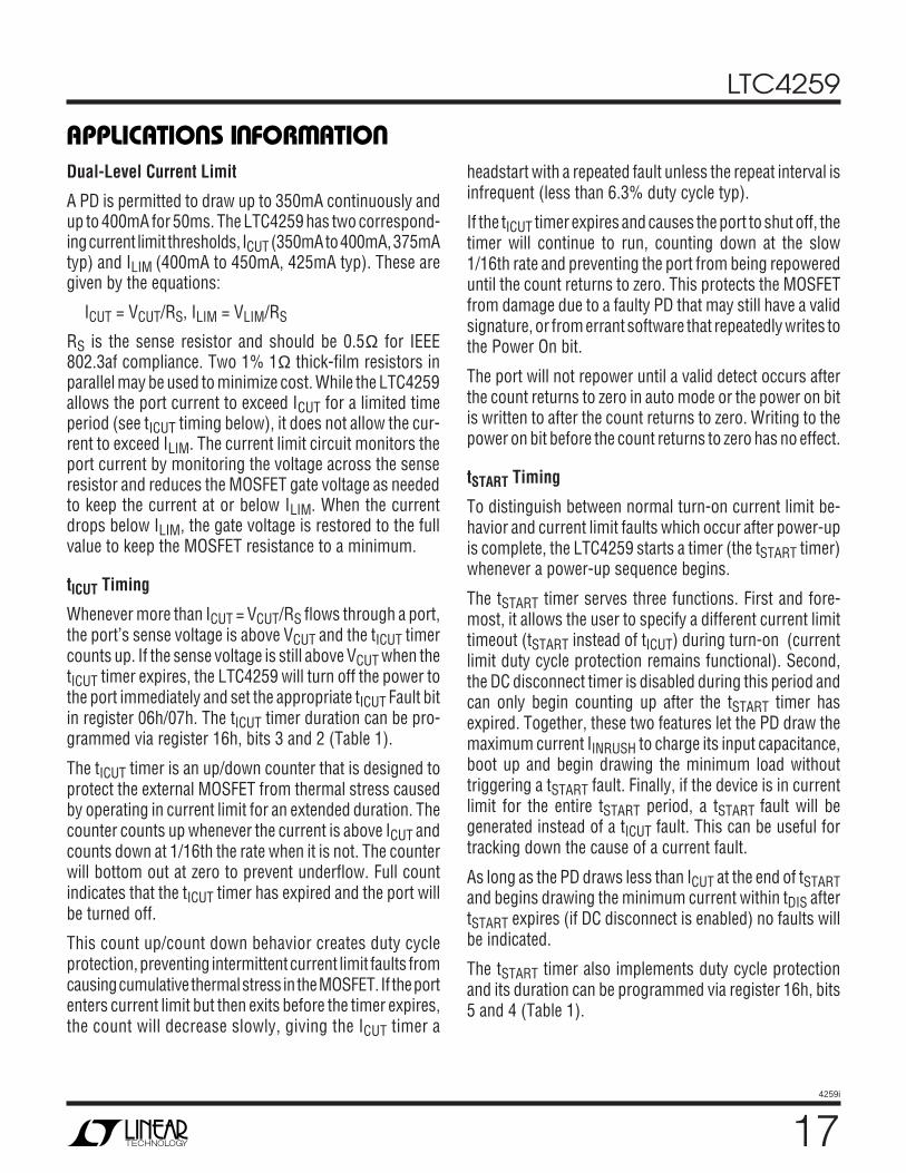
The LTC4259 implements a variety of current sense andlimit thresholds to control current flowing through theport. Figure 15 is a graphical representation of thesethresholds and the action the LTC4259 takes whencurrrent crosses the thresholds.
AC DISCONNECT
AC disconnect is an alternate method of sensing the pres-ence or absence of a PD by monitoring the port impedance.The LTC4259 forces a signal, amplified from the OSCIN pin,out of the DETECT pins and onto the Power over Ethernetconnection. It calculates the connection impedance fromohm’s law, ZPORT = VAC/IAC. Like DC disconnect, the AC dis-connect sensing circuitry controls the disconnect timer.When the connection impedance rises (AC current fallsbelow IACDMIN) due to the removal of the PD, the discon-nect timer counts up. If the impedance remains high (ACcurrent remains below IACDMIN), the disconnect timercounts to tDIS, the port is turned off and the port’s discon-nect bit in the Fault Register is set. If connection imped-ance falls (AC current rises above IACDMIN) before maximalcount of the disconnect timer, the timer resets and the portremains powered.
Like DC disconnect, AC disconnect can also be disabled byclearing the corresponding AC Discon Enable bits in theDisconnect register (13h). AC disconnect is also affectedby the tDIS duration programmed in register 16h.
Unlike DC disconnect, AC disconnect has no continuoustime output to the timer. Rather, AC disconnect will resetthe timer once every cycle, 1/fOSCIN, of the OSCIN signal ifthe port draws more than IACDMIN during that period.Because of this behavior, the time to turn off the port afterPD removal, tDIS, may be up to one cycle of OSCIN(1/fOSCIN) shorter than the delay programmed with thetDIS1 and tDIS0 bits. Note that AC disconnect and DCdisconnect signals that reset the tDIS timer are ORedtogether. Thus on a channel where both disconnect modesare enabled, either disconnect sensing method can keepthe port powered even if the other reports that there is noPD connected.
The AC disconnect circuitry senses the port and Powerover Ethernet connection from the DETECT pins. Connecta 0.22µF 100V X7R capacitor (CDET) and a 1k resistor(RDET) from the port’s DETECT pin to the port’s output asshown in Figure 16. This provides an AC path for sensingthe channel impedance. The 1k resistor, RDET, limitscurrent flowing through this path during port power onand power off.
Sizing of capacitors is critical to ensure proper function ofAC disconnect. CPSE (Figure 16) controls the connectionimpedance on the PSE side. Its capacitance must be keptlow enough for AC disconnect to be able to sense the PD.For operation near 100Hz, use a CPSE of 0.1µF or less. Onthe other hand, CDET has to be large enough to pass thesignal at the frequency of OSCIN. For fOSCIN ≈ 100Hz, useat least a 0.22µF 100V X7R capacitor. The sizes of CPSE,CDET, RDET and the frequency, fOSCIN, are chosen to createan economical, physically compact and functionallyrobust system. Moreover, the complete Power over Ether-net AC disconnect system (PSE, transformers, cabling,PD, etc.) is complex; deviating from the recommendedvalues of CDET, RDET and CPSE is discouraged. Contact theLTC Applications department for additional support.
APPLICATIO S I FOR ATIO
WU UU
Figure 15. LTC4259 Current Sense and Limits
0mA0mV
100mA
CURRENTRS = 0.5Ω
DC DIS-CONNECT
CUT(ICUT)
LIMIT(ILIM)
SHORTCIRCUIT
EFFECTSENSEnVOLTAGE
50mV
200mA100mV
300mA150mV
400mA200mV
500mA250mV
600mA300mV
CURRENTLIMIT
PORT OFF IN tICUT OR tSTART
PORT OFF IN 1µs
NORMALOPERATION
PORT OFF IN tDIS
4259 F15
LTC4259
214259i
When choosing CDET and CPSE, carefully consider voltagederating of the capacitors. Capacitors built around an X7Rdielectric will have about 60% of the specified capacitanceat their rated voltage. Operated at half their rated voltage,X7R capacitors exhibit more than 80% of their specifiedcapacitance. With other ceramic dielectrics commonlyused in 50V and 100V chip capacitors, capacitance fallsmuch more dramatically with voltage. At their rated volt-age, Y5V or Z5U capacitors exhibit less than 30% of theirzero-bias capacitance. In order to produce the desiredcapacitance at the operating bias, 100V X7R capacitorsshould be used with the LTC4259.
As illustrated in Figure 17, the Power over Ethernet con-nection between the PSE and PD includes a large amountof capacitance. Cable capacitance is particularly troublingbecause CAT-3 and CAT-5 pair-to-pair capacitance is not
tightly specified by the IEEE 802.3 standard or well con-trolled by cable manufacturers. Considering that patchpanels, additional connectors, old wiring, etc. are likely tobe placed between the PSE and PD, pair-to-pair capaci-tance is a pretty nebulous quantity. Consequently, theimpedance of the cable capacitance at the frequency usedfor AC disconnect can be a cause for concern. Assumimgthat fOSCIN is 100Hz, the 0.1µF of CPSE plus 0.05µF of cablecapacitance gives a port impedance of 10k at 100Hz. ThePD AC signature resistance is about 25k. Connecting a PDwith the maximum allowed resistance of 26.25k brings theconnection impedance to about 8k. The presence of a PDonly makes a 20% reduction in the port impedance. Withsome methods used for AC disconnect, cable capacitancecan fool the PSE into keeping the port powered. Fortu-nately, the LTC4259 has a solution to this problem. When
APPLICATIO S I FOR ATIO
WU UU
Figure 16. AC Disconnect Single Channel Application Circuit
Figure 17. Simplified AC Disconnect Circuit with Impedances at 100Hz
LEVELSHIFT
DETECT4
AGNDDGNDOSCIN
1/4LTC4259
–48V
GND
OUT4
ROUT410k
RS40.5Ω 1%
DDET41N4148
PD
RDET41k
Rpd_d ≤26.25k
Cpd_d ≥0.05k
CDET40.22µF100V X7R
CPSE40.1µF
100V X7R
4259 F16DAC4S1B
Q4
GATE4SENSE4VEE
OSCILLATORINPUT
CURRENTSENSE
RDET1k
<14k PD
~11k <30k
CDET0.22µF
CPSE ≤ 0.10µF CCABLE ≤ 0.05µF <30k Cpd_d ≥ 0.05µF Rpd_d < 26.25k
4259 F17
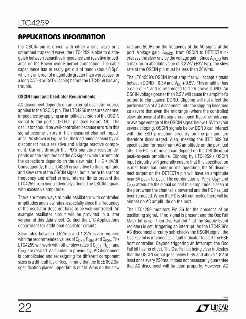
LTC4259
224259i
the OSCIN pin is driven with either a sine wave or asmoothed trapezoid wave, the LTC4259 is able to distin-guish between capacitive impedance and resistive imped-ance on the Power over Ethernet connection. The cablecapacitance has to really get out of hand (about 0.5µF,which is an order of magnitude greater than worst case fora long CAT-3 or CAT-5 cable) before the LTC4259 has anytrouble.
OSCIN Input and Oscillator Requirements
AC disconnect depends on an external oscillator sourceapplied to the OSCIN pin. The LTC4259 measures channelimpedance by applying an amplified version of the OSCINsignal to the port’s DETECT pin (see Figure 16). Theoscillator should be well-controlled because errors in thissignal become errors in the measured channel imped-ance. As shown in Figure 17, the load being sensed by ACdisconnect has a resistive and a large reactive compo-nent. Current through the PD’s signature resistor de-pends on the amplitude of the AC signal while current intothe capacitors depends on the slew rate; I = C • dV/dt.Consequently, the LTC4259 is sensitive to the amplitudeand slew rate of the OSCIN signal, but is more tolerant offrequency and offset errors. Internal limits prevent theLTC4259 from being adversely affected by OSCIN signalswith excessive amplitude.
There are many ways to build oscillators with controlledamplitudes and slew rates, especially since the frequencyof the oscillator does not have to be well-controlled. Anexample oscillator circuit will be provided in a laterversion of this data sheet. Contact the LTC Applicationsdepartment for additional oscillator circuits.
Slew rates between 0.5V/ms and 1.2V/ms are requiredwith the recommended values of CDET, RDET and CPSE. TheLTC4259 will work with other slew rates if CDET, RDET andCPSE are resized. As alluded to previously, AC disconnectis complicated and redesigning for different componentsizes is a difficult task. Keep in mind that the IEEE 802.3afspecification places upper limits of 100V/ms on the slew
rate and 500Hz on the frequency of the AC signal at theport. Voltage gain, AVACD, from OSCIN to DETECTn in-creases the slew rate by the voltage gain. Since AVACD hasa maximum absolute value of 3.3V/V (±3V typ), the slewrate at the OSCIN pin must be less than 30V/ms.
The LTC4259’s OSCIN input amplifier will accept signalsbetween DGND – 0.3V and VDD + 0.5V. This amplifier hasa gain of –1 and is referenced to 1.2V above DGND. AnOSCIN voltage greater than 2.2V will cause the amplifier’soutput to clip against DGND. Clipping will not affect theperformance of AC disconnect until the clipping becomesso severe that even the midrange (where the controlledslew rate occurs) of the signal is clipped. Keep the midrangeor average voltage of the OSCIN signal below 1.5V to avoidsevere clipping. OSCIN signals below DGND can interactwith the ESD protection circuitry on the pin and aretherefore discouraged. Also, meeting the IEEE 802.3afspecification for maximum AC amplitude on the port justafter the PD is removed can depend on the OSCIN inputpeak-to-peak amplitude. Clipping by LTC4259’s OSCINinput circuitry will generally ensure that this specificationis met. Note that under normal operation, the AC discon-nect output on the DETECTn pin will have an amplitudenear 6V peak-to-peak. The combination of RDET, CDET andCPSE attenuate the signal so half this amplitude is seen atthe port when the channel is powered and the PD has justbeen removed. When the PD is still connected there will bealmost no AC amplitude on the port.
The LTC4259 monitors Pin 36 for the presence of anoscillating signal. If no signal is present and the Osc FailMask bit is set, then Osc Fail (bit 1 of the Supply Eventregister) is set, triggering an interrupt. As the LTC4259’sAC disconnect circuitry self-checks the OSCIN signal, theOsc Fail bit is intended as a fault indicator to alert the PSEhost controller. Beyond triggering an interrupt, the OscFail bit has no effect. The Osc Fail bit being clear indicatesthat the OSCIN signal goes below 0.6V and above 1.8V atleast once every 250ms. It does not necessarily guaranteethat AC disconnect will function properly. However, AC
APPLICATIO S I FOR ATIO
WU UU
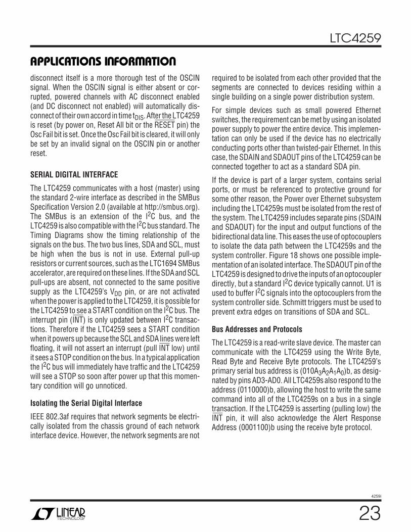
LTC4259
234259i
APPLICATIO S I FOR ATIO
WU UU
disconnect itself is a more thorough test of the OSCINsignal. When the OSCIN signal is either absent or cor-rupted, powered channels with AC disconnect enabled(and DC disconnect not enabled) will automatically dis-connect of their own accord in time tDIS. After the LTC4259is reset (by power on, Reset All bit or the RESET pin) theOsc Fail bit is set. Once the Osc Fail bit is cleared, it will onlybe set by an invalid signal on the OSCIN pin or anotherreset.
SERIAL DIGITAL INTERFACE
The LTC4259 communicates with a host (master) usingthe standard 2-wire interface as described in the SMBusSpecification Version 2.0 (available at http://smbus.org).The SMBus is an extension of the I2C bus, and theLTC4259 is also compatible with the I2C bus standard. TheTiming Diagrams show the timing relationship of thesignals on the bus. The two bus lines, SDA and SCL, mustbe high when the bus is not in use. External pull-upresistors or current sources, such as the LTC1694 SMBusaccelerator, are required on these lines. If the SDA and SCLpull-ups are absent, not connected to the same positivesupply as the LTC4259’s VDD pin, or are not activatedwhen the power is applied to the LTC4259, it is possible forthe LTC4259 to see a START condition on the I2C bus. Theinterrupt pin (INT) is only updated between I2C transac-tions. Therefore if the LTC4259 sees a START conditionwhen it powers up because the SCL and SDA lines were leftfloating, it will not assert an interrupt (pull INT low) untilit sees a STOP condition on the bus. In a typical applicationthe I2C bus will immediately have traffic and the LTC4259will see a STOP so soon after power up that this momen-tary condition will go unnoticed.
Isolating the Serial Digital Interface
IEEE 802.3af requires that network segments be electri-cally isolated from the chassis ground of each networkinterface device. However, the network segments are not
required to be isolated from each other provided that thesegments are connected to devices residing within asingle building on a single power distribution system.
For simple devices such as small powered Ethernetswitches, the requirement can be met by using an isolatedpower supply to power the entire device. This implemen-tation can only be used if the device has no electricallyconducting ports other than twisted-pair Ethernet. In thiscase, the SDAIN and SDAOUT pins of the LTC4259 can beconnected together to act as a standard SDA pin.
If the device is part of a larger system, contains serialports, or must be referenced to protective ground forsome other reason, the Power over Ethernet subsystemincluding the LTC4259s must be isolated from the rest ofthe system. The LTC4259 includes separate pins (SDAINand SDAOUT) for the input and output functions of thebidirectional data line. This eases the use of optocouplersto isolate the data path between the LTC4259s and thesystem controller. Figure 18 shows one possible imple-mentation of an isolated interface. The SDAOUT pin of theLTC4259 is designed to drive the inputs of an optocouplerdirectly, but a standard I2C device typically cannot. U1 isused to buffer I2C signals into the optocouplers from thesystem controller side. Schmitt triggers must be used toprevent extra edges on transitions of SDA and SCL.
Bus Addresses and Protocols
The LTC4259 is a read-write slave device. The master cancommunicate with the LTC4259 using the Write Byte,Read Byte and Receive Byte protocols. The LTC4259’sprimary serial bus address is (010A3A2A1A0)b, as desig-nated by pins AD3-AD0. All LTC4259s also respond to theaddress (0110000)b, allowing the host to write the samecommand into all of the LTC4259s on a bus in a singletransaction. If the LTC4259 is asserting (pulling low) theINT pin, it will also acknowledge the Alert ResponseAddress (0001100)b using the receive byte protocol.
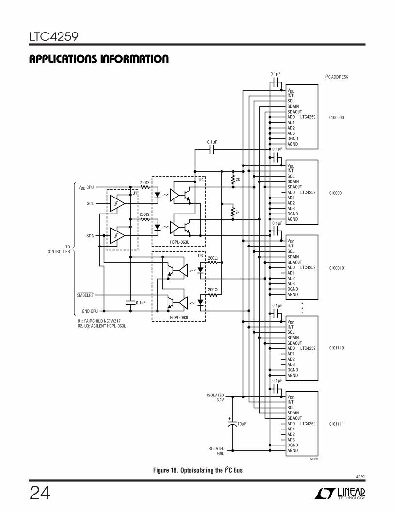
LTC4259
244259i
Figure 18. Optoisolating the I2C Bus
APPLICATIO S I FOR ATIO
WU UU4258 F18
VDDINTSCLSDAINSDAOUTAD0AD1AD2AD3DGNDAGND
LTC4259
VDDINTSCLSDAINSDAOUTAD0AD1AD2AD3DGNDAGND
LTC4259
VDDINTSCLSDAINSDAOUTAD0AD1AD2AD3DGNDAGND
LTC4259
VDDINTSCLSDAINSDAOUTAD0AD1AD2AD3DGNDAGND
LTC4259
VDDINTSCLSDAINSDAOUTAD0AD1AD2AD3DGNDAGND
LTC4259
•••
0.1µF
0.1µF
0.1µF
0.1µF
0.1µF
+10µF
2k
2k
0.1µF
0.1µF
200Ω
200Ω
200Ω
200Ω
U2
U3
U1
HCPL-063L
HCPL-063L
VDD CPU
SCL
SDA
SMBELRT
GND CPU
U1: FAIRCHILD NC7WZ17U2, U3: AGILENT HCPL-063L
TOCONTROLLER
ISOLATED3.3V
ISOLATEDGND
0100000
0100001
0100010
0101110
0101111
I2C ADDRESS
LTC4259
254259i
The START and STOP Conditions
When the bus is idle, both SCL and SDA must be high. Abus master (typically the host system) signals the begin-ning of a communication to a slave device (like theLTC4259) by transmitting a START condition. A STARTcondition is generated by transitioning SDA from high tolow while SCL is high. When the master has finishedcommunicating with the slave, it issues a STOP condition.A STOP condition is generated by transitioning SDA fromlow to high while SCL is high. The bus is then free forcommunication with another SMBus or I2C device.
Acknowledge
The Acknowledge signal is used for handshaking betweenthe master and the slave. An Acknowledge (active LOW)generated by the slave lets the master know that the latestbyte of information was received. The corresponding SCLclock pulse is always generated by the master. The masterreleases the SDA line (HIGH) during the Acknowledgeclock pulse. The slave must pull down the SDA line duringthe Acknowledge clock pulse so that it remains a stableLOW during the HIGH period of this clock pulse. When themaster is reading from a slave device, it is the master’sresponsibility to acknowledge receipt of the data byte inthe bit that follows unless the transaction is complete. Inthat case the master will decline to acknowledge and issuethe STOP condition to terminate the communication.
Write Byte Protocol
The master initiates communication to the LTC4259 witha START condition and a 7-bit bus address followed by theWrite Bit (Wr) = 0. If the LTC4259 recognizes its ownaddress, it acknowledges and the master delivers the com-mand byte, signifying to which internal LTC4259 registerthe master wishes to write. The LTC4259 acknowledgesand latches the lower five bits of the command byte into itsRegister Address register. Only the lower five bits of thecommand byte are checked by the LTC4259; the upperthree bits are ignored. The master then delivers the databyte. The LTC4259 acknowledges once more and latchesthe data into the appropriate control register. Finally, the
master terminates the communication with a STOP condi-tion. Upon reception of the STOP condition, the RegisterAddress register is cleared (see Figure 7).
Read Byte Protocol
The master initiates communication from the LTC4259with a START condition and the same 7-bit bus addressfollowed by the Write Bit (Wr) = 0. If the LTC4259recognizes its own address, it acknowledges and themaster delivers the command byte, signifying whichinternal LTC4259 register it wishes to read from. TheLTC4259 acknowledges and latches the lower five bits ofthe command byte into its Register Address register. Atthis time the master sends a REPEATED START conditionand the same 7-bit bus address followed by the Read Bit(Rd) = 1. The LTC4259 acknowledges and sends thecontents of the requested register. Finally, the masterdeclines to acknowledge and terminates communicationwith a STOP condition. On the reception of the STOPcondition, the Register Address register is cleared (seeFigure 8).
Receive Byte Protocol
Since the LTC4259 clears the Register Address register oneach STOP condition, the interrupt register (register 0)may be read with the Receive Byte Protocol as well as withthe Read Byte Protocol. In this protocol, the masterinitiates communication with the LTC4259 with a STARTcondition and a 7-bit bus address followed by the Read Bit(Rd) = 1. The LTC4259 acknowledges and sends thecontents of the interrupt register. The master then de-clines to acknowledge and terminates communicationwith a STOP condition (see Figure 9).
Alert Response Address and the INT Pin
In a system where several LTC4259s share a common INTline, the master can use the Alert Response Address (ARA)to determine which LTC4259 initiated the interrupt.
The master initiates the ARA procedure with a STARTcondition and the 7-bit ARA bus address (0001100)bfollowed by the Read Bit (Rd) = 1. If an LTC4259 is
APPLICATIO S I FOR ATIO
WU UU
LTC4259
264259i
asserting the INT pin, it acknowledges and sends its 7-bitbus address (010A3A2A1A0)b and a 1 (see Figure 10).While it is sending its address, it monitors the SDAIN pinto see if another device is sending an address at the sametime using standard I2C bus arbitration. If the LTC4259 issending a 1 and reads a 0 on the SDAIN pin on the risingedge of SCL, it assumes another device with a loweraddress is sending and the LTC4259 immediately abortsits transfer and waits for the next ARA cycle to try again.If transfer is successfully completed, the LTC4259 willstop pulling down the INT pin. When the INT pin is releasedin this way or if a 1 is written into the Clear Interrupt pin bit(bit 6 of register 1Ah), the condition causing the LTC4259to pull the INT pin down must be removed before theLTC4259 will be able to pull INT down again. This can bedone by reading and clearing the event registers or bywriting a 1 into the Clear All Interrupts bit (bit 7 of register1Ah). The state of the INT pin can only change between I2Ctransactions, so an interrupt is cleared or new interruptsare generated after a transaction completes and beforenew I2C bus communication commences. Periodic pollingof the alert response address can be used instead of theINT pin if desired. If any device acknowledges the alertresponse address, then the INT line, if connected, wouldhave been low.
System Software Strategy
Control of the LTC4259 hinges on one decision, theLTC4259’s operating mode. The three choices are de-scribed under Operating Modes. In Auto mode the LTC4259can operate autonomously without direction from a hostcontroller. Because LTC4259s running in Auto mode willpower every valid PD connected to them, the PSE musthave 15.4W/port available. To reduce the power require-ments of the –48V supply, PSE systems can track powerusage, only turning on ports when sufficient power isavailable. The IEEE describes this as a power allocationalgorithm and places two limitations: the PSE shall notpower a PD unless it can supply the maximum power forthat PD’s class and power allocation may not be based
APPLICATIO S I FOR ATIO
WU UU
solely on a history of each PD’s power consumption. Inorder for a PSE to implement power allocation, the PSE’sprocessor/controller must control whether ports are pow-ered—the LTC4259’s cannot operate in Auto mode.Semiauto mode fits the bill as the LTC4259 automaticallydetects and classifies PDs and makes this informationavailable to the host controller, which decides to applypower or not. Operating the LTC4259 in Manual mode alsolets the controller decide whether to power the ports butthe controller must also control detection and classifica-tion. If the host controller operates near the limit of itscomputing resources, it may not be able to guide a Manualmode LTC4259 through detect, class and port turn-on inless than the IEEE maximum of 950ms.
In a typical PSE, the LTC4259s will operate in Semiautomode as this allows the host to decide to power a portwithout burdening the controller. With an interrupt maskof F4h, the LTC4259 will signal to the host after it hassuccessfully detected and classed a PD, at which point thehost can decide whether enough power is available andcommand the LTC4259 to turn that port on. Similarly, theLTC4259 will generate interrupts when a port’s power isturned off. By reading the LTC4259’s interrupt register,the host can determine if a port was turned off due toovercurrent (tSTART or tICUT faults) or because the PD wasremoved (Disconnect event). The host then updates theamount of available power to reflect the power no longerconsumed by the disconnected PD. Setting the MSB ofthe interrupt mask causes the LTC4259 to communicatefault conditions caused by failures within the PSE, so thehost does not need to poll to check that the LTC4259s areoperating properly. This interrupt driven system architec-ture provides the controller with the final say on poweringports at the same time, minimizing the controller’s com-putation requirements because interrupts are only gener-ated when a PD is discovered or on a fault condition.
The LTC4259 can also be used to power older poweredEthernet devices that are not 802.3af compliant and maybe detected with other methods. Although the LTC4259
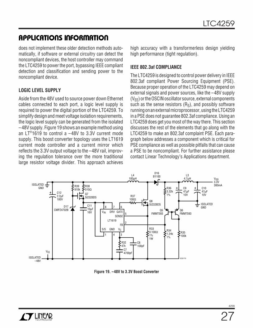
LTC4259
274259i
does not implement these older detection methods auto-matically, if software or external circuitry can detect thenoncompliant devices, the host controller may commandthe LTC4259 to power the port, bypassing IEEE compliantdetection and classification and sending power to thenoncompliant device.
LOGIC LEVEL SUPPLY
Aside from the 48V used to source power down Ethernetcables connected to each port, a logic level supply isrequired to power the digital portion of the LTC4259. Tosimplify design and meet voltage isolation requirements,the logic level supply can be generated from the isolated–48V supply. Figure 19 shows an example method usingan LT®1619 to control a –48V to 3.3V current modesupply. This boost converter topology uses the LT1619current mode controller and a current mirror whichreflects the 3.3V output voltage to the –48V rail, improv-ing the regulation tolerance over the more traditionallarge resistor voltage divider. This approach achieves
high accuracy with a transformerless design yieldinghigh performance (tight regulation).
IEEE 802.3af COMPLIANCE
The LTC4259 is designed to control power delivery in IEEE802.3af compliant Power Sourcing Equipment (PSE).Because proper operation of the LTC4259 may depend onexternal signals and power sources, like the –48V supply(VEE) or the OSCIN oscillator source, external componentssuch as the sense resistors (RS), and possibly softwarerunning on an external microprocessor, using the LTC4259in a PSE does not guarantee 802.3af compliance. Using anLTC4259 does get you most of the way there. This sectiondiscusses the rest of the elements that go along with theLTC4259 to make an 802.3af complaint PSE. Each para-graph below addresses a component which is critical forPSE compliance as well as possible pitfalls that can causea PSE to be noncompliant. For further assistance pleasecontact Linear Technology’s Applications department.
APPLICATIO S I FOR ATIO
WU UU
DRV
R37100Ω
L4100µH
L34.7µH
D16B1100
C1110µF16V
C74700pF
C8100pF
D17CMPZ4702B
ISOLATEDGND
ISOLATED–48V
Q8Si2328DS
Q5FMMT593
Q6FMMT593
8 7 6
5
2
341
GATEVIN
VCS/S
SENSELT1619
FBGND
Q7Si2328DS
R38510Ω
R3247k
R363.32k1%
R330.100Ω1%1W
R341.24k1%
R35100k
4259 F19
R39910k
C122.2µF100V
+
VEE
C947µF10V
VDD3.3V300mA
+ C1047µF10V
ISOLATEDGND
+
Figure 19. –48V to 3.3V Boost Converter
LTC4259
284259i
APPLICATIO S I FOR ATIO
WU UU
Sense Resistors
The 0.5Ω resistors (RS) used to sense the current througha port affect the current limit and all thresholds for apowered port. An error in the value of a sense resistor cancause noncompliance to the IEEE specifications for IINRUSH/ILIM, ICUT and IMIN. The value of the RS resistor has beenkept small to minimize power loss, allowing low costresistors to be used. As a consequence, the SENSE volt-ages which the LTC4259 must measure are small. At thesame time up to 450mA may be flowing through the senseresistors and associated circuit board traces. To preventparasitic resistance of the circuit board’s traces fromobscuring the voltage drop across the sense resistor, theLTC4259 must Kelvin sense the sense resistor voltage.One way to achieve Kelvin sensing is “star grounding,”shown pictorially in Figure 1. Another option is to connectthe sense resistor and the LTC4259’s VEE pin to a –48Vpower plane in the circuit board. Either or these strategieswill prevent voltages developed across parasitic circuitboard resistances from affecting the LTC4259’s currentsense.
Power MOSFETs
The LTC4259 controls power MOSFETs in order to regu-late current flow through the Ethernet ports. Under certainconditions these MOSFETs have to dissipate significantpower. See the Choosing External MOSFETs section for adetailed discussion of the requirements these devicesmust meet.
Common Mode Chokes
Both nonpowered and powered Ethernet connectionsachieve best performance (for data transfer, power trans-fer and EMI) when a common mode choke is used on eachport. In the name of cost reduction, some designs share acommon mode choke between two adjacent ports. Evenfor nonpowered Ethernet, sharing a choke is not recom-mended. Now that two ports pass through the choke, itcannot limit the common mode current of either port.Rather the choke only controls the sum of both portscommon mode current. Because cabling from the ports
generally connects to different devices up to 200m apart,a current loop can form. In such a loop, common modecurrent flows in one port and out the other, and choke willnot stop it because the sum of the currents is zero. Anotherway to view this interaction between the paired ports isthat the choke acts as a transformer coupling the portscommon modes together. In nonpowered Ethernet com-mon mode current results from nonidealities like groundloops; it is not part of normal operation. However Powerover Ethernet sends power and hence significant currentthrough the ports; common mode current is a byproductof normal operation. As described in the Choosing Exter-nal MOSFETs section and under the Power Suppliesheading below, large transients can occur when a port’spower is turned on or off. When a powered port is shorted(see Surge Suppressors and Circuit Protection), a port’scommon mode current may be excessive. Sharing acommon mode choke between two ports couples start-up, disconnect and fault transients from one port to theother. The end result can range from momentary noncom-pliance with 802.3af to intermittent behavior and even toexcessive voltages that may damage circuitry (in both thePSE and PD) connected to the ports.
Detect, AC Blocking and Transient Supressor Diodes
During detection and classification, the LTC4259 sensesthe port voltage through the detect diodes, DDET in Figure16. Excessive voltage drop across DDET will corrupt theLTC4259’s detect and classification results. Select a diodefor DDET that will have less than 0.7V of forward drop at0.4mA and less than 1V of forward drop at 50mA.
The AC blocking diodes can interfere with AC disconnectsensing if they become leaky. If the AC blocking diode, DACin Figure 16, begins leaking, it contributes to the Ethernetport impedance, potentially bringing the impedance lowenough to draw IACDMIN from the DETECT pin and keep theport powered. More likely, leakage through the AC block-ing diode will cause shifts in the AC disconnect thresholdthat are not large enough to make the PSE noncompliant.Generally, diode leakage is caused by voltage or tempera-ture stress. Diodes that are rated to 100V or more and can
LTC4259
294259i
handle dissipating at least 0.5W should not be stressed inthis application. Other component leakages can have asimilar affect on AC disconnect and affect DC disconnectif the leakage becomes more severe. Among componentsto be wary of are the transient surge suppressors. Thedevices shown in Figure 1 are rated for less than 5µA ofleakage at 58V. However there is a potential for stressinduced leakage, so healthy margins should be used whenselecting diodes for these applications.
Capacitors
Sizing of both the CDET and CPSE capacitors is critical toproper operation of the LTC4259’s AC disconnect sensing.See the AC Disconnect section for more information. Also,CPSE may be important to the voltage stability of a poweredport. Port voltage instability is generally not a problem if VEE,the –48V supply, is well bypassed. For both of these rea-sons be aware that many ceramic dielectrics have dramaticcapacitance versus DC voltage coefficients. A 0.22µF ce-ramic capacitor is often nowhere near 0.22µF when oper-ating at 50VDC or 100VDC. Use 100V or higher rated X7Rcapacitors for CDET and CPSE as these have reduced volt-age dependance while also being small and inexpensive.
Power Supplies
The LTC4259 must be supplied with 3.3V (VDD) and –48V(VEE). Poor regulation on either of these supplies can leadto noncompliance. The IEEE requires a PSE output voltagebetween 44V and 57V. Allowing for voltage drop, mostlyacross the AC blocking diodes DAC between VEE and thePSE’s Ethernet jacks, means that VEE must be morenegative than –45V (more if DAC has more than 1V offorward drop). When the LTC4259 begins powering anEthernet port, it controls the current through the port tominimize disturbances on VEE. However if the VEE supplyis underdamped or otherwise unstable, its voltage couldgo outside of the IEEE specified limits causing all ports inthe PSE to be noncompliant. This scenario can be evenworse when a PD is unplugged because the current dropsimmediately to zero. In both cases the VEE supply must
APPLICATIO S I FOR ATIO
WU UU
always stay between –45V and –57V. In addition, the802.3af specification places specific ripple, noise and loadregulation requirements on the PSE. Among other things,disturbances on either VDD or VEE can adversely affectdetection, classification and the AC disconnection sens-ing. In short, proper bypassing and stability of the VDD andVEE supplies are important.
Another problem that can affect the VEE supply is insuffi-cient power, leading to the supply voltage drooping out ofthe specified range. The 802.3af specification states thatif a PSE powers a PD it must be able to provide themaximum power level requested by the PD based on thePD’s classification. The specification does allow a PSE tochoose not to power a port because the PD requires morepower than the PSE has left to deliver. If a PSE is built witha VEE supply capable of less than 15.4W • (number ofPSE’s Ethernet ports), it must implement a power alloca-tion algorithm that prevents ports from being poweredwhen there is insufficient power. Because the specifica-tion also requires the PSE to supply 400mA at up to a 5%duty cycle, the VEE supply capability should be at least afew percent more than the maximum total power the PSEwill supply to PDs. Finally, the LTC4259’s draw currentfrom VEE. If the VDD supply is generated from VEE, thatpower divided by the switcher efficiency must be added tothe VEE supply’s capability; (33mW ÷ efficiency • [numberof PSE’s Ethernet ports] ÷ 4) typically less than 12mW/port.
AC disconnect also relies on an oscillating signal appliedto the OSCIN pin. Requirements for this signal are pro-vided in the OSCIN Input and Oscillator Requirementssection. Out-of-band noise on the OSCIN pin will disruptthe LTC4259’s ability to sense the absence of a PD. Anynoise present at the OSCIN pin is amplified by the LTC4259and driven out of the DETECT pins (of powered ports withAC disconnect enabled). Due to the amount of capacitanceconnected to the DETECT pins, driving this noise caneasily require more than IACDMIN, tripping the DETECT pincurrent sense and keeping the port powered. Duringcircuit board layout, keep wiring from the oscillator to theOSCIN pin away from noise sources like digital clock and
LTC4259
304259i
APPLICATIO S I FOR ATIO
WU UU
data lines. Also a single-stage RC lowpass filter (shown inFigure 20) will attenuate out-of-band noise. There won’t bemuch voltage drop across the RC filter because the imped-ance of the OSCIN pin is high, typically 500k.
CONCLUSION
The LTC4259 provides the precision analog circuitry andlogic necessary to build IEEE 803.3af compliant Powerover Ethernet power sourcing equipment (PSE). Therequirements placed on the PSE are complex and the
LTC4259 handles most of them but there are elements ofthe PSE that are beyond the LTC4259’s control.
These potential compliance pitfalls can be avoided duringcircuit design and layout by paying attention to the issuesmentioned above. In addition, consider checking for IEEE802.3af compliance after subjecting the PSE to real-worldfault conditions: ESD and cable discharge events, shortedports, connecting to an already powered port, powersupply glitches and so on. Linear Technology’s Applica-tions department can also provide additional support.

LTC4259
314259i
U
PACKAGE DESCRIPTIOGW Package
36-Lead Plastic SSOP (Wide .300 Inch)(Reference LTC DWG # 05-08-1642)
GW36 SSOP 0502
0° – 8° TYP
0.231 – 0.3175(.0091 – .0125)
0.610 – 1.016(.024 – .040)
7.417 – 7.595**(.292 – .299)
× 45°0.254 – 0.406(.010 – .016)
2.286 – 2.387(.090 – .094)
0.127 – 0.305(.005 – .0115)
2.463 – 2.641(.097 – .104)
0.800(.0315)
BSC
0.304 – 0.431(.012 – .017)
15.290 – 15.544*(.602 – .612)
1 2 3 4 5 6 7 8 9 10 11 12 13 14 15 16 17 18
10.160 – 10.414(.400 – .410)
36 35 34 33 32 31 30 29 28 27 26 25 24 23 22 21 20 19
10.668 MIN
RECOMMENDED SOLDER PAD LAYOUT
7.416 – 7.747
0.800 TYP0.520 ±0.0635
1.143 ±0.127
DIMENSION DOES NOT INCLUDE MOLD FLASH. MOLD FLASH SHALL NOT EXCEED 0.152mm (0.006") PER SIDE
*
DIMENSION DOES NOT INCLUDE INTERLEAD FLASH. INTERLEAD FLASH SHALL NOT EXCEED 0.254mm (0.010") PER SIDE
**MILLIMETERS
(INCHES)
NOTE:1. CONTROLLING DIMENSION: MILLIMETERS
2. DIMENSIONS ARE IN
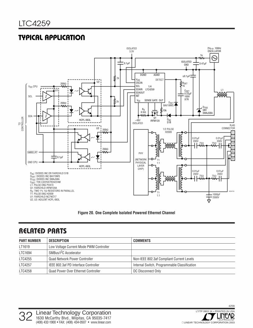
LTC4259
324259i
Linear Technology Corporation1630 McCarthy Blvd., Milpitas, CA 95035-7417(408) 432-1900 FAX: (408) 434-0507 www.linear.com LINEAR TECHNOLOGY CORPORATION 2003
LT/TP 0803 1K • PRINTED IN USA
RELATED PARTSPART NUMBER DESCRIPTION COMMENTS
LT1619 Low Voltage Current Mode PWM Controller
LTC1694 SMBus/I2C Accelerator
LTC4255 Quad Network Power Controller Non-IEEE 802.3af Compliant Current Levels
LTC4257 IEEE 802.3af PD Interface Controller Internal Switch, Programmable Classification
LTC4258 Quad Power Over Ethernet Controller DC Disconnect Only
4258 F20
12345678
2k
2k
0.1µF
0.1µF
200Ω
200Ω
200Ω
200Ω
U2
U3
U1
HCPL-063L
HCPL-063L
VDD CPU
SCL
SDA
SMBELRT
GND CPU
DAC: DIODES INC OR FAIRCHILD S1BDDET: DIODES INC BAV19WSDTSS: DIODES INC SMAJ58ACDET: TDK C3225X7R2A224ML1: PULSE ENG PO473Q1: FAIRCHILD IRFM120ARS: TWO 1% 1Ω RESISTORS IN PARALLELT1: PULSE ENG H2009U1: FAIRCHILD NC7WZ17U2, U3: AGILENT HCPL-063L
TOCO
NTRO
LLER
PHY
(NETWORKPHYSICAL
LAYERCHIP)
DTSS58VSMAJ58A
≤0.1µF
0.47µF
1k
VEE SENSE GATE OUT
VDDOSCINSCLSDAINSDAOUTINT
DDETBAV19WS
10k
DACS1B
RDET1k
L1CDET0.22µF100VX7R
RS0.5Ω
Q1IRFM120
1/4LTC4259
DGND AGND
DETECT
–48VISOLATED
ISOLATED3.3V
ISOLATEDGND
2VP-P, 100HzOSCILLATOR
0.01µF200V
0.01µF200V
0.01µF200V
0.01µF200V
75Ω75Ω
75Ω75Ω
RJ45CONNECTOR1/2 PULSE
H2009
T11:1
T11:1 1000pF
2000V
Figure 20. One Complete Isolated Powered Ethernet Channel
TYPICAL APPLICATIO
U


![[PPT]Fast Ethernet and Gigabit Ethernet - WPIweb.cs.wpi.edu/~rek/Undergrad_Nets/B04/Fast_Ethernet.ppt · Web viewFast Ethernet and Gigabit Ethernet Fast Ethernet (100BASE-T) How to](https://img.pdfslide.net/doc/110x75/5b29d4a97f8b9aad2f8b4e9d/pptfast-ethernet-and-gigabit-ethernet-rekundergradnetsb04fastethernetppt.jpg)