Embed Size (px)
Citation preview
All trademarks and logos are property of their respective owners. All rights reserved. They are here used only as conceptual examples
Power Semiconductors technologies
trends for E-Mobility
All trademarks and logos are property of their respective owners. All rights reserved. They are here used only as conceptual examples
Gianni Vitale
Power Conversion & Drives Section Manager
System Lab, STMicroelectronics
NESEM 2013, Toulouse
1
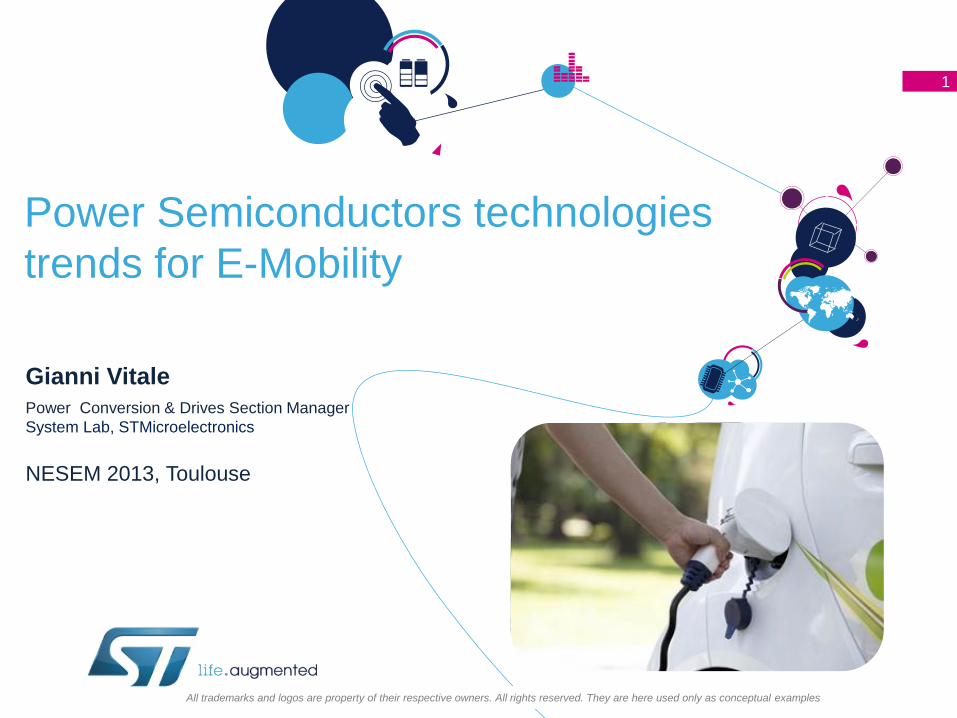
Outline 2
• Semiconductor Market Outlook in Automotive
• Technology positioning for E-Vehicles applications
• Silicon Technology Evolution
• Low Voltage MOSFETs
• High Voltage MOSFETs
• IGBTS
• New WBG Materials (SiC & GaN)
• Next Steps & Challenges
2

Semiconductor Market Outlook in
Automotive
3
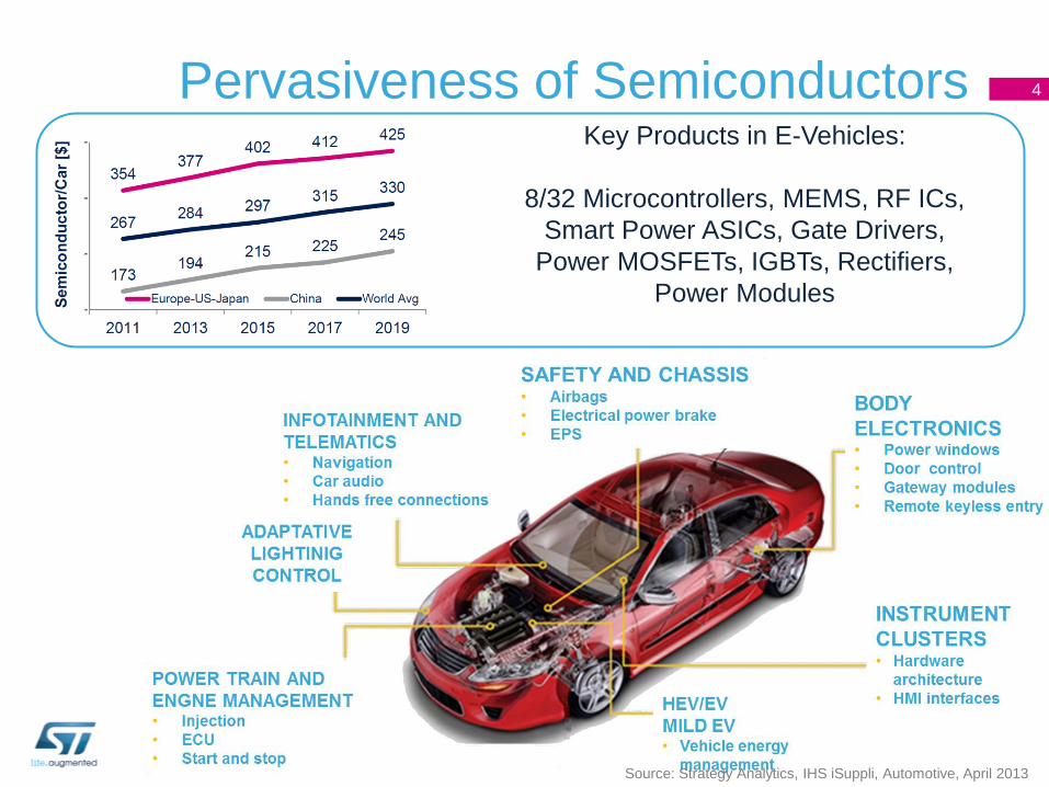
Pervasiveness of Semiconductors 4
Source: Strategy Analytics, IHS iSuppli, Automotive, April 2013
Key Products in E-Vehicles:
8/32 Microcontrollers, MEMS, RF ICs,
Smart Power ASICs, Gate Drivers,
Power MOSFETs, IGBTs, Rectifiers,
Power Modules
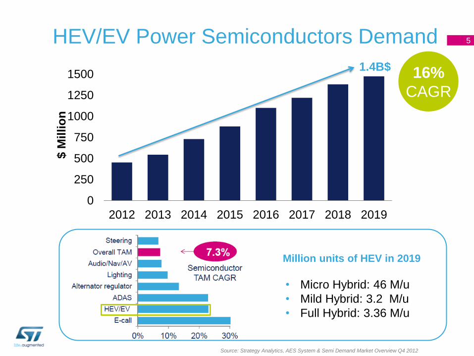
HEV/EV Power Semiconductors Demand
0
250
500
750
1000
1250
1500
2012 2013 2014 2015 2016 2017 2018 2019
$ M
illi
on
16%
CAGR
Source: Strategy Analytics, AES System & Semi Demand Market Overview Q4 2012
5
1.4B$
Million units of HEV in 2019
• Micro Hybrid: 46 M/u
• Mild Hybrid: 3.2 M/u
• Full Hybrid: 3.36 M/u
Technology positioning for E-Vehicles applications
6
All trademarks and logos are property of their respective owners. All rights reserved. They are here used only as conceptual examples
Electric Vehicles main blocks 7
by degree of hybridization
M Air-con
inverter
M ICE cooling
inverter
Power
steering
inverter M
On-board
charger
Fast charging
(DC)
Home
outlet
(AC)
(Not in HEV)
HV battery pack
(200V to 450V)
Cells
balancing
Traction
inverter
El motor /
generator
ICE
(no EV)
DC/DC
converter
HEV
ECU
Hybrid drive
unit (HDU)
HV Bus
DC/DC
converter
Aux LV
battery
(12V or 24V)
Battery module
Aux. DC/DC converters
Power: 1.5kW-4kW
Main inverters
Power: 10kW-100kW
On Board Charger
Power: 1.5kW-50KW
BU
S <
60V
B
US
>60V
Micro-Hybrid
Mild-Hybrid
Full-Hybrid Can run on just ICE, just
batteries, combination of both
ICE with Start/Stop, electrical
assistance, regenerative braking
ICE with Start/Stop and
(optionally) regenerative breaking
Fast
Charger
Smart
Meter
PLM ISO15118
Fast
charging
(DC)
Three
phase
mains
(AC)
Fast Charger
Power: 50kW-100KW
All trademarks and logos are property of their respective owners. All rights reserved. They are here used only as conceptual examples
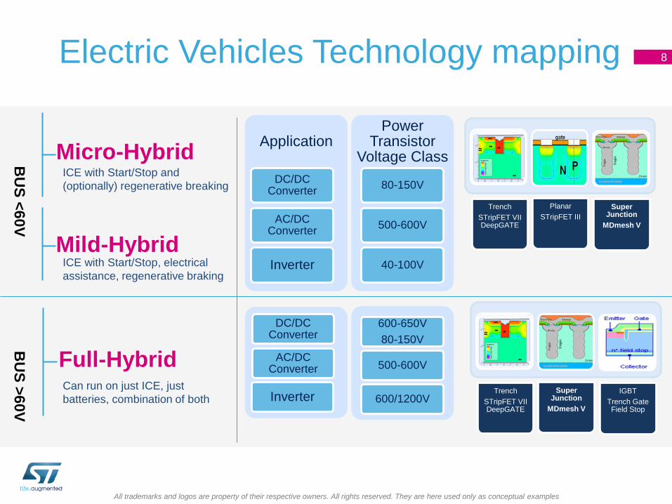
Electric Vehicles Technology mapping 8
Micro-Hybrid
Mild-Hybrid
Full-Hybrid Can run on just ICE, just
batteries, combination of both
ICE with Start/Stop, electrical
assistance, regenerative braking
ICE with Start/Stop and
(optionally) regenerative breaking
BU
S <
60V
Application
DC/DC Converter
AC/DC Converter
Inverter
Power Transistor
Voltage Class
80-150V
500-600V
40-100V
DC/DC Converter
AC/DC Converter
Inverter
600-650V
80-150V
500-600V
600/1200V
Trench
STripFET VII DeepGATE
Planar
STripFET III
Super Junction
MDmesh V
Trench
STripFET VII DeepGATE
Super Junction
MDmesh V
IGBT
Trench Gate Field Stop
BU
S >
60V

Silicon Technology Evolution
9
All trademarks and logos are property of their respective owners. All rights reserved. They are here used only as conceptual examples
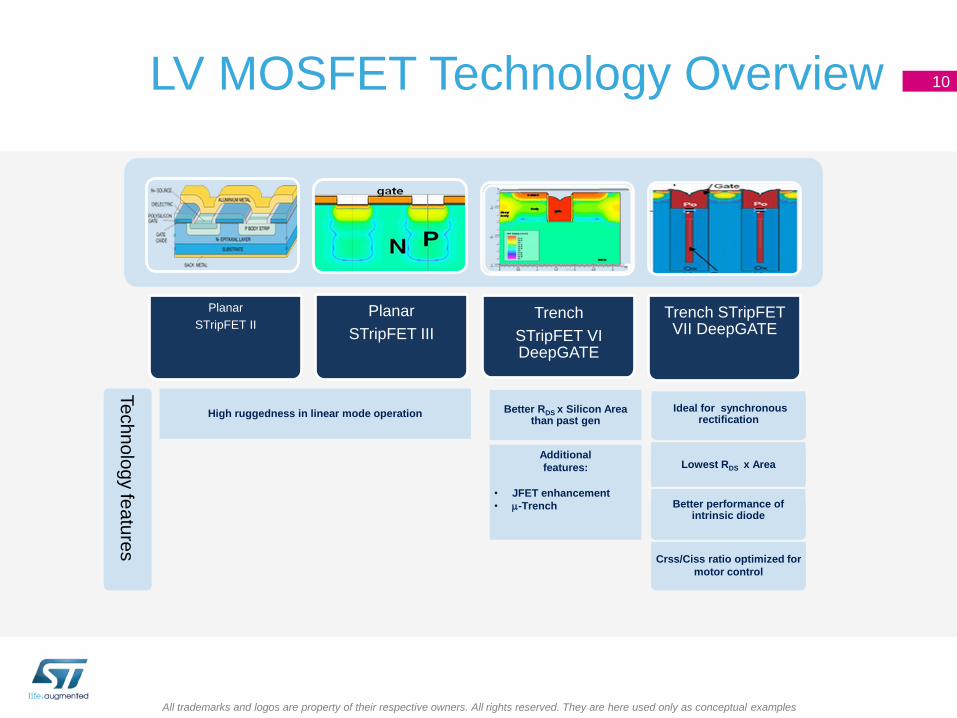
Planar
STripFET II Planar
STripFET III
Trench
STripFET VI DeepGATE
Trench STripFET VII DeepGATE
Te
ch
no
log
y fe
atu
res
Ideal for synchronous rectification
Additional
features:
• JFET enhancement
• m-Trench
Better RDS x Silicon Area than past gen
Lowest RDS x Area
Better performance of intrinsic diode
Crss/Ciss ratio optimized for
motor control
High ruggedness in linear mode operation
LV MOSFET Technology Overview 10
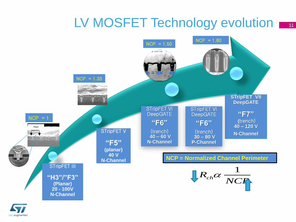
STripFET III
“H3”/”F3” (Planar)
20 - 100V N-Channel
STripFET V
“F5” (planar)
40 V N-Channel
STripFET VI DeepGATE
“F6”
(trench) 40 – 60 V N-Channel
STripFET VII DeepGATE
“F7” (trench)
40 – 120 V
N-Channel
LV MOSFET Technology evolution 11
NCP = 1.50
NCP = 1
Pitch
NCP = 1.33
NCP = 1.80
NCP = Normalized Channel Perimeter
NCPRch
1
STripFET VI DeepGATE
“F6”
(trench) 30 – 80 V P-Channel
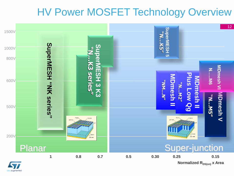
500V
1000V
1500V
800V
600V
200V
Normalized RDS(on) x Area
1 0.8 0.7 0.5 0.30 0.15 0.25
Super-junction
Su
pe
rME
SH
“N
K s
erie
s”
Planar
Su
pe
rME
SH
3 K
3
“N
…K
3 s
erie
s”
HV Power MOSFET Technology Overview
MD
mesh
II
“N
M…
N”
MD
me
sh
II
Plu
s L
ow
Qg
“N
…M
2”
Su
pe
rME
SH
5
“N
…K
5”
MD
mesh
V
“N
…M
5”
MD
mesh
VI
N…
..M6
12
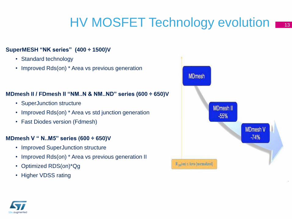
HV MOSFET Technology evolution 13
SuperMESH “NK series” (400 ÷ 1500)V
• Standard technology
• Improved Rds(on) * Area vs previous generation
MDmesh II / FDmesh II “NM..N & NM..ND” series (600 ÷ 650)V
• SuperJunction structure
• Improved Rds(on) * Area vs std junction generation
• Fast Diodes version (Fdmesh)
MDmesh V “ N..M5” series (600 ÷ 650)V
• Improved SuperJunction structure
• Improved Rds(on) * Area vs previous generation II
• Optimized RDS(on)*Qg
• Higher VDSS rating
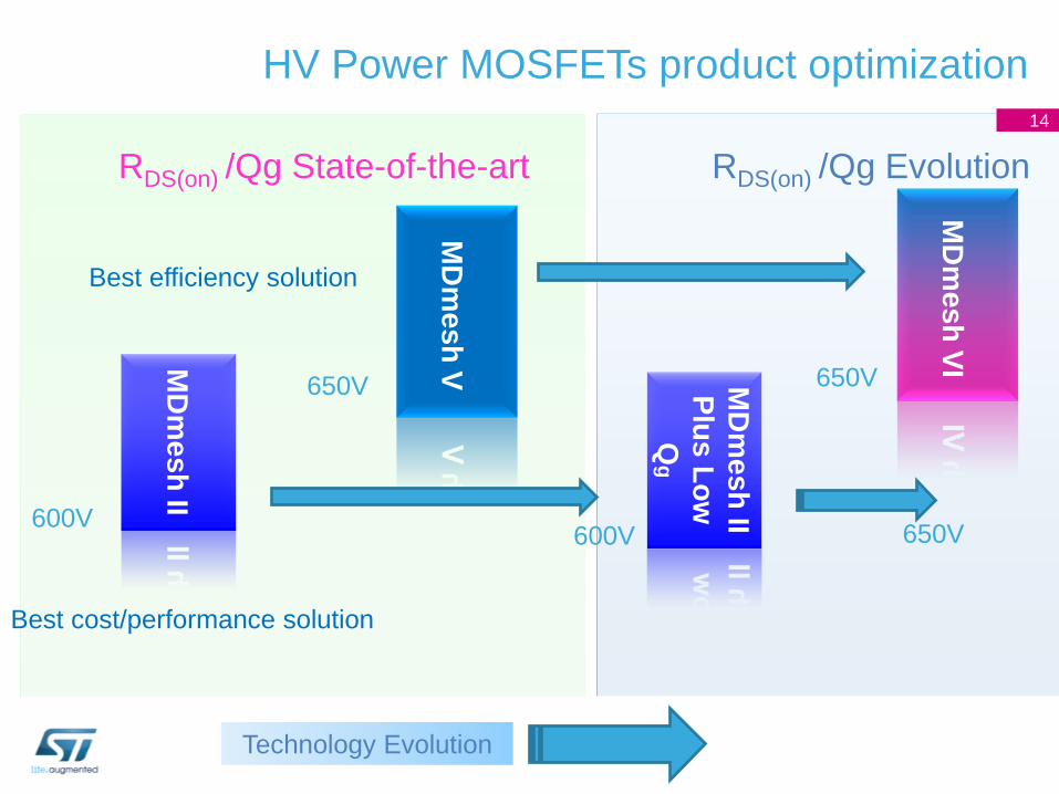
RDS(on) /Qg State-of-the-art
Best cost/performance solution
HV Power MOSFETs product optimization
MD
me
sh
II
MD
me
sh
VI
RDS(on) /Qg Evolution
MD
me
sh
V
MD
me
sh
II
Plu
s L
ow
Qg
650V
600V 600V
Best efficiency solution
650V
Technology Evolution
650V
14
All trademarks and logos are property of their respective owners. All rights reserved. They are here used only as conceptual examples
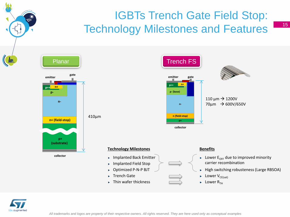
IGBTs Trench Gate Field Stop:
Technology Milestones and Features 15
Planar
410µm
collector
emitter gate
n-
n+ (field-stop)
p-
p++ n+
p+ (substrate)
Technology Milestones
Implanted Back Emitter
Implanted Field Stop
Optimized P-N-P BJT
Trench Gate
Thin wafer thickness
Benefits
Lower EOFF due to improved minority carrier recombination
High switching robusteness (Large RBSOA)
Lower VCE(sat)
Lower RTH
110 µm 1200V 70µm 600V/650V n-
n (field-stop)
p- (base)
p++ n+
collector
emitter gate
p+
Trench FS
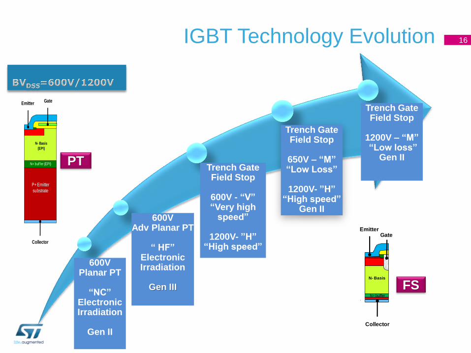
600V Planar PT
“NC”
Electronic Irradiation
Gen II
600V Adv Planar PT
“ HF”
Electronic Irradiation
Gen III
Trench Gate Field Stop
600V - “V” “Very high
speed”
1200V- ”H” “High speed”
Trench Gate Field Stop
650V – “M” “Low Loss”
1200V- ”H”
“High speed” Gen II
Trench Gate Field Stop
1200V – “M” “Low loss”
Gen II
IGBT Technology Evolution 16
Gate
Collector
Emitter
N- Basis
N+ buffer
Collector
EmitterGate
N+ buf fer (EPI)
P+ Emitter
substrate
N- Basis
(EPI)
FS
PT
New WBG Materials (SiC & GaN)
17
All trademarks and logos are property of their respective owners. All rights reserved. They are here used only as conceptual examples
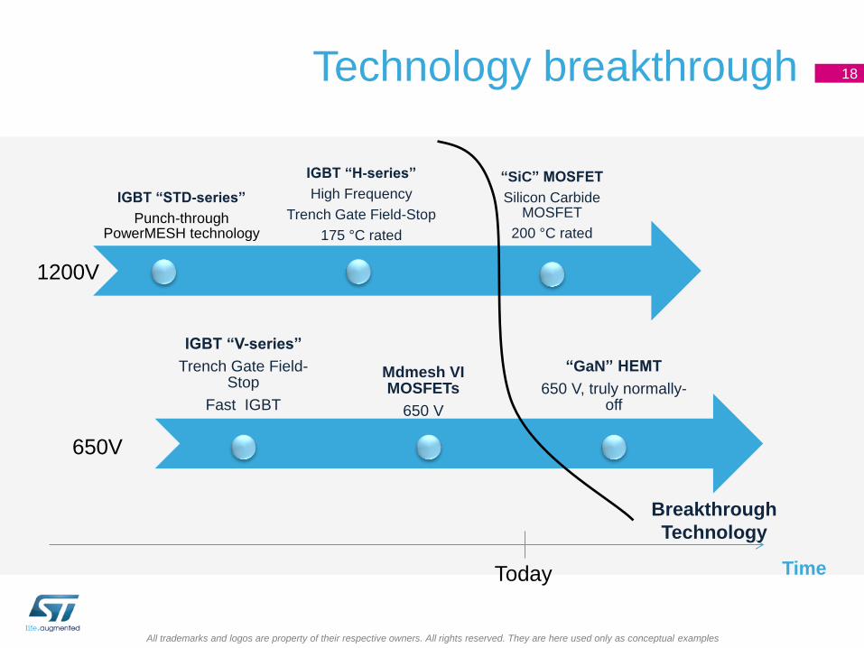
IGBT “STD-series”
Punch-through PowerMESH technology
IGBT “H-series”
High Frequency
Trench Gate Field-Stop
175 °C rated
“SiC” MOSFET
Silicon Carbide MOSFET
200 °C rated
IGBT “V-series”
Trench Gate Field-Stop
Fast IGBT
Mdmesh VI MOSFETs
650 V
“GaN” HEMT
650 V, truly normally-off
18
Time Today
Breakthrough
Technology
650V
1200V
Technology breakthrough
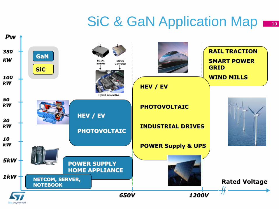
650V 1200V
Rated Voltage 1kW
5kW
10 kW
30 kW
50 kW
100 kW
350
KW
Pw
NETCOM, SERVER, NOTEBOOK
POWER SUPPLY HOME APPLIANCE
HEV / EV
PHOTOVOLTAIC
HEV / EV
PHOTOVOLTAIC
INDUSTRIAL DRIVES
POWER Supply & UPS
RAIL TRACTION
SMART POWER GRID
WIND MILLS
GaN
SiC
LV & SJ TAM
SiC & GaN Application Map 19
All trademarks and logos are property of their respective owners. All rights reserved. They are here used only as conceptual examples
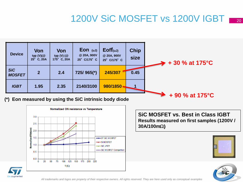
1200V SiC MOSFET vs 1200V IGBT
SiC
Device Von
typ (V)(@
25°C, 20A
Von typ (V) (@
175°C, 20A
Eon (uJ)
@ 20A, 900V
25°C/175°C
Eoff(uJ)
@ 20A, 900V
25°C/175°C
Chip
size
SiC
MOSFET 2 2.4 725/ 965(*) 245/307 0.45
IGBT 1.95 2.35 2140/3100 980/1850 1
SiC MOSFET vs. Best in Class IGBT Results measured on first samples (1200V /
30A/100m)
(*) Eon measured by using the SiC intrinsic body diode
+ 30 % at 175°C
+ 90 % at 175°C
20
All trademarks and logos are property of their respective owners. All rights reserved. They are here used only as conceptual examples
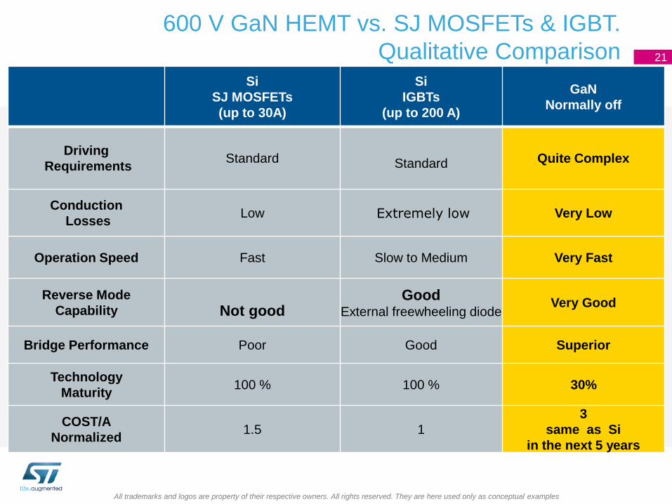
600 V GaN HEMT vs. SJ MOSFETs & IGBT.
Qualitative Comparison
21
Si
SJ MOSFETs
(up to 30A)
Si
IGBTs
(up to 200 A)
GaN
Normally off
Driving
Requirements Standard
Standard
Quite Complex
Conduction
Losses Low Extremely low Very Low
Operation Speed Fast Slow to Medium Very Fast
Reverse Mode
Capability
Not good Good
External freewheeling diode Very Good
Bridge Performance Poor Good Superior
Technology
Maturity 100 % 100 % 30%
COST/A
Normalized 1.5 1
3
same as Si
in the next 5 years
All trademarks and logos are property of their respective owners. All rights reserved. They are here used only as conceptual examples
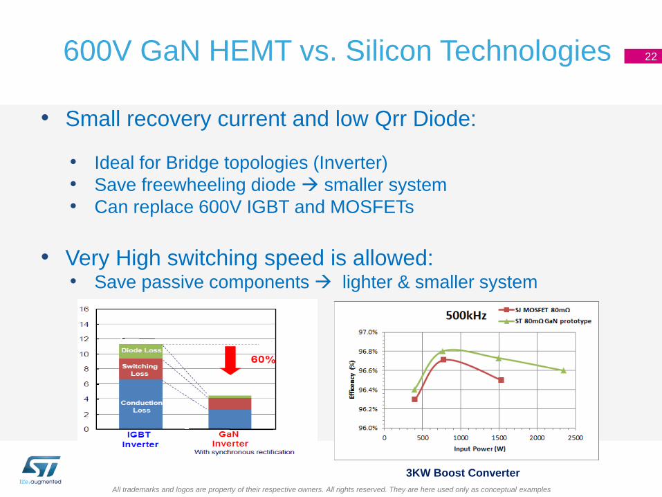
600V GaN HEMT vs. Silicon Technologies
• Small recovery current and low Qrr Diode:
• Ideal for Bridge topologies (Inverter)
• Save freewheeling diode smaller system
• Can replace 600V IGBT and MOSFETs
• Very High switching speed is allowed: • Save passive components lighter & smaller system
3KW Boost Converter
22
All trademarks and logos are property of their respective owners. All rights reserved. They are here used only as conceptual examples
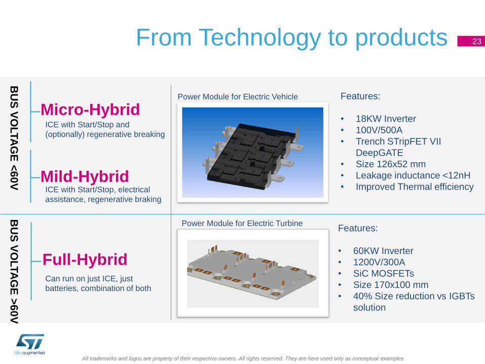
From Technology to products 23
Micro-Hybrid
Mild-Hybrid
Full-Hybrid Can run on just ICE, just
batteries, combination of both
ICE with Start/Stop, electrical
assistance, regenerative braking
ICE with Start/Stop and
(optionally) regenerative breaking
BU
S V
OLTA
GE
<60
V
BU
S V
OLTA
GE
>60
V
Features:
• 60KW Inverter
• 1200V/300A
• SiC MOSFETs
• Size 170x100 mm
• 40% Size reduction vs IGBTs
solution
Power Module for Electric Turbine
Power Module for Electric Vehicle Features:
• 18KW Inverter
• 100V/500A
• Trench STripFET VII
DeepGATE
• Size 126x52 mm
• Leakage inductance <12nH
• Improved Thermal efficiency
All trademarks and logos are property of their respective owners. All rights reserved. They are here used only as conceptual examples
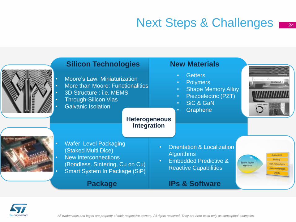
Heterogeneous Integration
• Getters
• Polymers
• Shape Memory Alloy
• Piezoelectric (PZT)
• SiC & GaN
• Graphene
Next Steps & Challenges 24
• Wafer Level Packaging
(Staked Multi Dice)
• New interconnections
(Bondless. Sintering, Cu on Cu)
• Smart System In Package (SiP)
• Moore’s Law: Miniaturization
• More than Moore: Functionalities
• 3D Structure : i.e. MEMS
• Through-Silicon Vias
• Galvanic Isolation
• Orientation & Localization
Algorithms
• Embedded Predictive &
Reactive Capabilities
C
New Materials Silicon Technologies
Package IPs & Software