Embed Size (px)
Citation preview
Page 1 of 15
EE 409/691: RF Comm. Lab
Lecture 4: September 4, 2000
Experiment 3 - 2nd lab on S parameter measurements
By the time you complete this lab you will be familiar with the use of the network analyzer
We are going to use the equipment seen - the network analyzer and components
2 passive componentspower splitter (ZAPD-2)hybrid coupler (MIDISCO DC72)
1 active componentamplifier (ZFL-2000)
power splitters and hybrid couplers are used in microwave and rf subsystems
Pre-lab
1) Define the following terms:insertion lossreturn lossSWRphase balancemagnitude balancegainisolationcoupling
Page 2 of 15
Page 3 of 15
Page 4 of 15
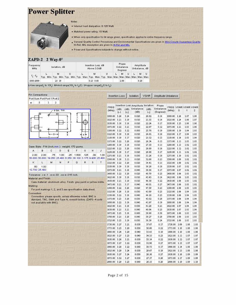
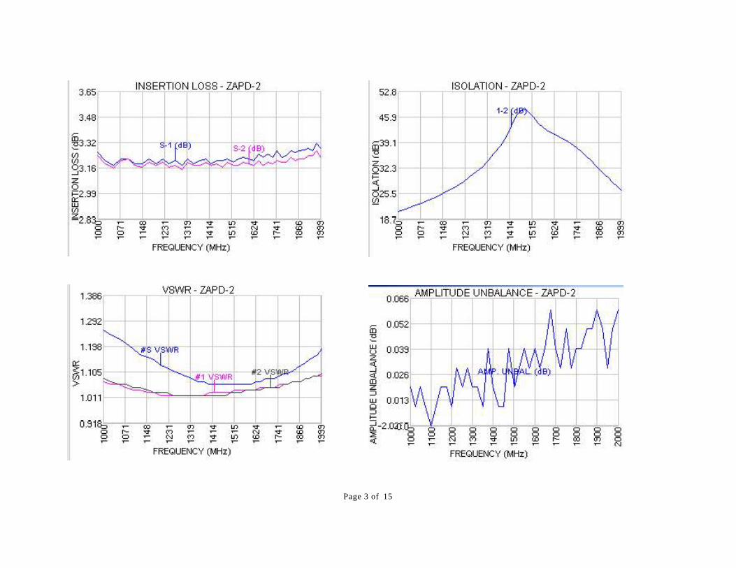
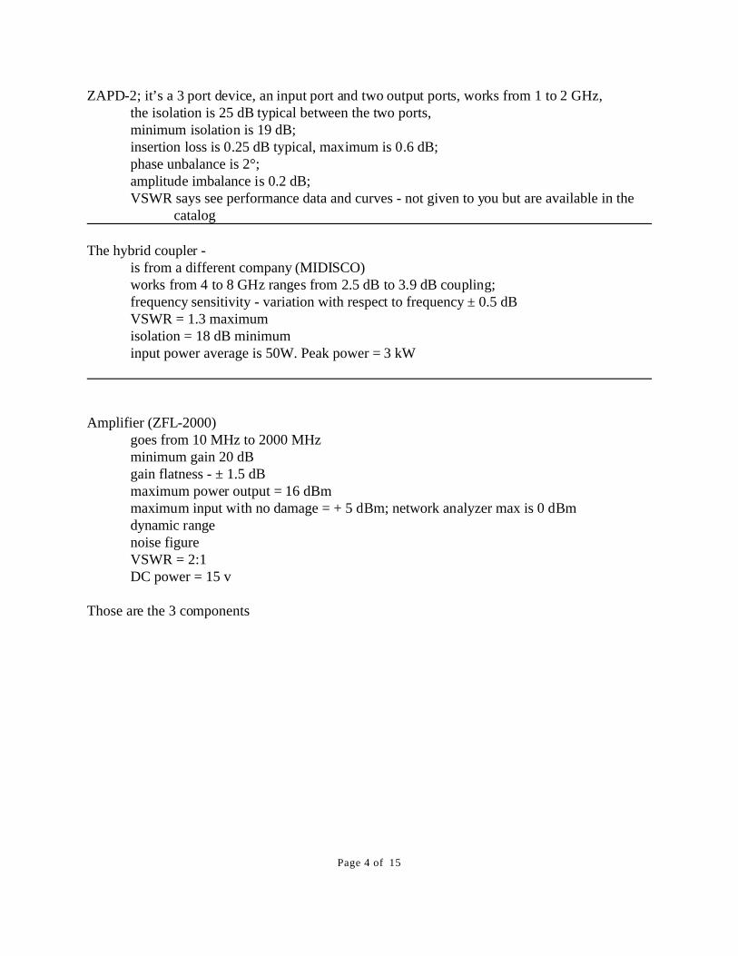
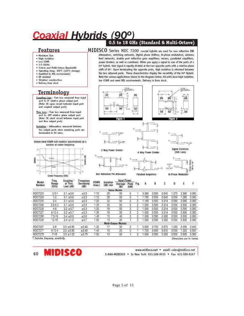
ZAPD-2; it’s a 3 port device, an input port and two output ports, works from 1 to 2 GHz,the isolation is 25 dB typical between the two ports,minimum isolation is 19 dB;insertion loss is 0.25 dB typical, maximum is 0.6 dB;phase unbalance is 2°;amplitude imbalance is 0.2 dB;VSWR says see performance data and curves - not given to you but are available in the
catalog
The hybrid coupler - is from a different company (MIDISCO)works from 4 to 8 GHz ranges from 2.5 dB to 3.9 dB coupling;frequency sensitivity - variation with respect to frequency ± 0.5 dBVSWR = 1.3 maximumisolation = 18 dB minimuminput power average is 50W. Peak power = 3 kW
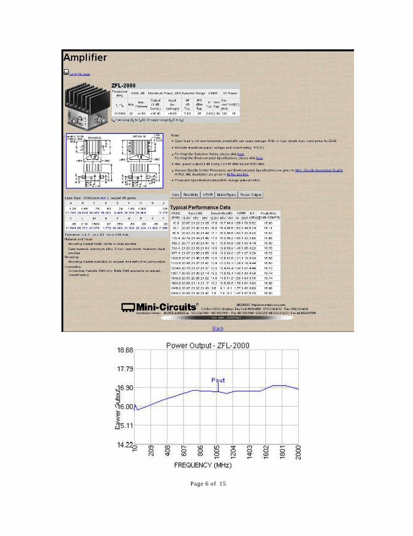
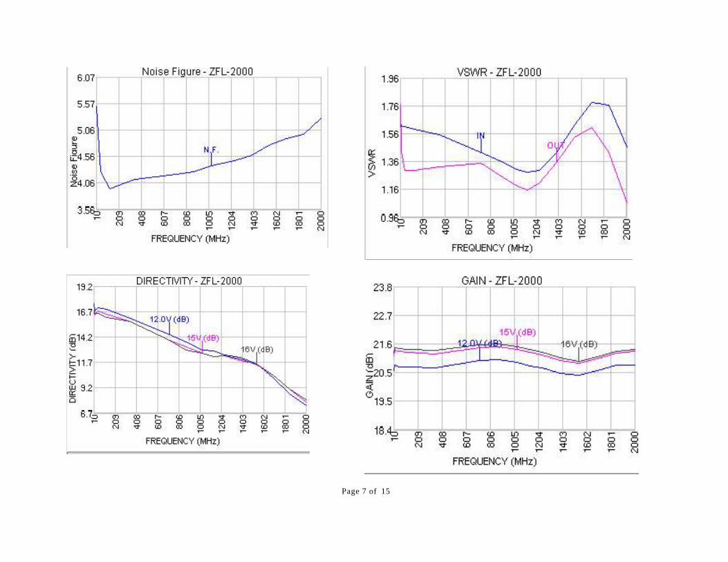
Amplifier (ZFL-2000)goes from 10 MHz to 2000 MHzminimum gain 20 dBgain flatness - ± 1.5 dBmaximum power output = 16 dBm maximum input with no damage = + 5 dBm; network analyzer max is 0 dBmdynamic rangenoise figureVSWR = 2:1DC power = 15 v
Those are the 3 components
Page 5 of 15
Page 6 of 15
Page 7 of 15
Page 8 of 15
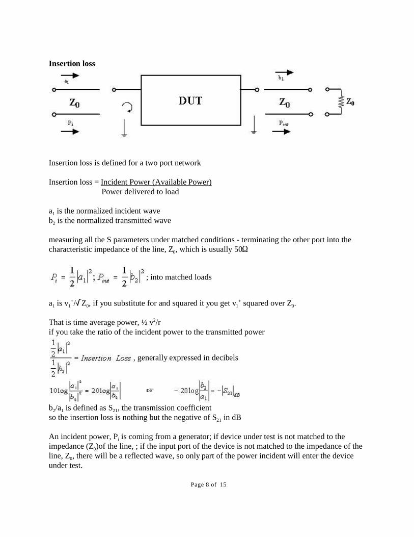
Insertion loss
Insertion loss is defined for a two port network
Insertion loss = Incident Power (Available Power) Power delivered to load
a1 is the normalized incident waveb2 is the normalized transmitted wave
measuring all the S parameters under matched conditions - terminating the other port into thecharacteristic impedance of the line, Z0, which is usually 50S
; into matched loads
a1 is v1+//Z0, if you substitute for and squared it you get v1
+ squared over Z0.
That is time average power, ½ v2/rif you take the ratio of the incident power to the transmitted power
, generally expressed in decibels
L
b2/a1 is defined as S21, the transmission coefficientso the insertion loss is nothing but the negative of S21 in dB
An incident power, Pi is coming from a generator; if device under test is not matched to theimpedance (Z0)of the line, ; if the input port of the device is not matched to the impedance of theline, Z0, there will be a reflected wave, so only part of the power incident will enter the deviceunder test.
Page 9 of 15
Say Pi = 10 mW, 1 mW is reflected, only 9 mW will go to the device under test. The 9 mW maybe attenuated further in the device. Any passive device - a filter, splitter - will have resistivecomponents, so 9 mW may not come out of the second port. This is known as loss due toattenuation.
The power reflected back right at the port is also considered as a loss. This is not a loss in thesame way as losing energy due to resistive losses, but is a loss in the sense that some power is notaccepted by the device, it is sent back; this is known as return loss - we will talk about this later.
So there is some loss due to mismatch, there is some loss due to attenuation inside the device, ifport 2 is not matched to the transmission line, then there is no maximum transfer of power to theline, so there is also a loss due to mismatch. The impedance seen looking into a source mustequal the impedance looking into the load for a maximum transfer of power.
There could be a mismatch loss at port 1, a mismatch loss at port 2 and loss of energy(attenuation) through the device. This total is known as insertion loss.
Suppose this device were not present - and the two lines were connected directly and they wereperfectly matched - there would be no loss. By inserting this device into the system, you arecreating a loss due to mismatch and attenuation. All the losses taken together are considered asthe insertion loss.
How do you know if the mismatch is considered? If we considered the loss through the device,we would be looking at only the attenuation. The insertion loss represents the total loss created bythe insertion of the device - mathematically, this is nothing more than S21.
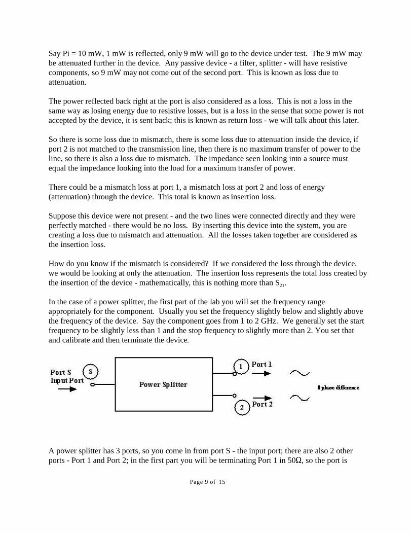
In the case of a power splitter, the first part of the lab you will set the frequency rangeappropriately for the component. Usually you set the frequency slightly below and slightly abovethe frequency of the device. Say the component goes from 1 to 2 GHz. We generally set the startfrequency to be slightly less than 1 and the stop frequency to slightly more than 2. You set thatand calibrate and then terminate the device.
A power splitter has 3 ports, so you come in from port S - the input port; there are also 2 otherports - Port 1 and Port 2; in the first part you will be terminating Port 1 in 50S, so the port is

Page 10 of 15
closed by termination. You are converting this 3 port device into a 2 port device, so Port 2 andPort S are available. The S parameters are determined between these 2 ports; the S port isconnected to port 1 of the network analyzer and port 2 is connected to port 2 of the networkanalyzer. You measure S21 between ports 2 and 2, the S parameters 2-1 refer to the networkanalyzer ports. You can number these in a different way - 4, 5, or 6. As far as the networkanalyzer is concerned, whatever is connected to its port 1is port 1, etc.
If you measure S21between ports S and 2; the negative of S21 in dB, for example, - 3 dB, is theinsertion loss L then the insertion loss is +3 dB; it is just a convention that insertion loss isexpressed as a positive number. Since it’s expressed as a positive number, multiply by a negativesign.
What does a power splitter do? It divides the power equally between ports 1 and 2. P1 = P2; P1 = ½ PS; P2 = ½ PS
The power at port 1 is ½ of the power at the input port, Port S, and the power at port 2 is ½ thepower at Port S.
PS/P1 = 2, or 3 dB, or the power at port 1 is 3 dB below the input power, and likewise for port 2. This is nothing but the insertion loss.
We assume that most of these components are very well matched to 50 S at their ports. Theamount of reflection, or mismatch, at these ports is minimum. You will find out when youdetermine SWR. There is some amount of loss in the power splitter, so you may not get exactly 3dB for the S21, you may get less than 3 dB.
An ideal power splitter will split equally, or the S21 will be 3 dB below PS; it may be 3.3 or 3.4dB;the extra 0.3 or 0.4 represent the attenuation of the power splitter. Magnitude wise you should getthe same power.
Phase wise they should have the same phase. The phase of the wave coming out of Port 1 shouldbe x degrees, and the phase of the wave coming out of Port 2 should also be x degrees. The phasedifference between the output ports of the power splitter ideally should be 0°. Any phasedifference (deviation) between the ports is known as the phase balance.
Suppose the difference between them is 3 or 4 degrees, then you say that the phase balance is 0 ±3 or 4 °. It means the phase difference varies between by 3 and 4 degrees over the frequencyband.
Remember in a power splitter that the magnitudes of the power at the output ports should be thesame, and the phase difference should be 0. How do you determine the phase?
The magnitude of S21 should be the same. A difference of S21 between ports 1 and 2 of the phasesplitter is known as the magnitude balance. A difference of phase between the 2 ports is known as
Page 11 of 15
the phase balance.
Normally when you do the S parameters, you get the plots on the screen which you print, you canalso get the data in a table format. If you want to find the information accurately, it is very hard toget that information from the plots, unless you put several markers at different frequencies. Oryou can print a set of values, and print a table format.
One caution in printing a table is you should set the printout for 51 points; printing too manypoints will take a long time and is not necessary, so keep the number of points small.
The magnitude balance is the difference is magnitudes in dB between the 2 ports, and phasebalance is the difference in phase in degrees between the two ports.
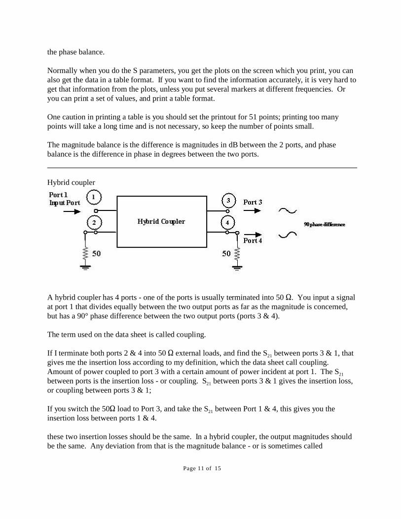
Hybrid coupler
A hybrid coupler has 4 ports - one of the ports is usually terminated into 50 S. You input a signalat port 1 that divides equally between the two output ports as far as the magnitude is concerned,but has a 90° phase difference between the two output ports (ports 3 & 4).
The term used on the data sheet is called coupling.
If I terminate both ports 2 & 4 into 50 S external loads, and find the S21 between ports 3 & 1, thatgives me the insertion loss according to my definition, which the data sheet call coupling. Amount of power coupled to port 3 with a certain amount of power incident at port 1. The S21
between ports is the insertion loss - or coupling. S21 between ports 3 & 1 gives the insertion loss,or coupling between ports 3 & 1;
If you switch the 50S load to Port 3, and take the S21 between Port 1 & 4, this gives you theinsertion loss between ports 1 & 4.
these two insertion losses should be the same. In a hybrid coupler, the output magnitudes shouldbe the same. Any deviation from that is the magnitude balance - or is sometimes called
Page 12 of 15
magnitude imbalance. If one is -3 dB, the other should be -3 dB. The difference between theports should be 0 dB.
How do you calculate the phase difference?
In the case of the power splitter, you can look at the phase plots between ports S & 1 and S & 2;superimpose the plots over one another, and you should not see any difference.
In a hybrid coupler, there should be ideally 90° phase difference between the ports. In a practicalhybrid coupler, it may be 85 or 100°. Usually the phase balance in a hybrid coupler or othercouplers where the difference is 180°, in such cases, the phase balance is specified as 90° ± somany degrees over the frequency range.
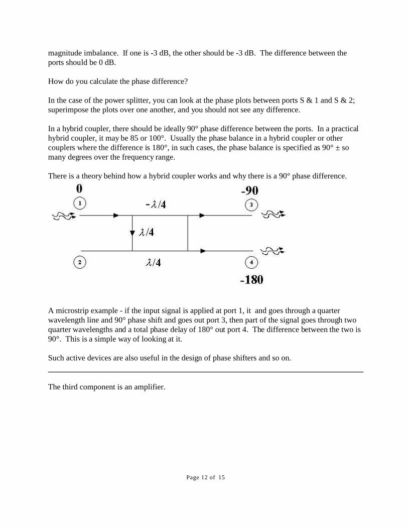
There is a theory behind how a hybrid coupler works and why there is a 90° phase difference.
A microstrip example - if the input signal is applied at port 1, it and goes through a quarterwavelength line and 90° phase shift and goes out port 3, then part of the signal goes through twoquarter wavelengths and a total phase delay of 180° out port 4. The difference between the two is90°. This is a simple way of looking at it.
Such active devices are also useful in the design of phase shifters and so on.
The third component is an amplifier.
Page 13 of 15
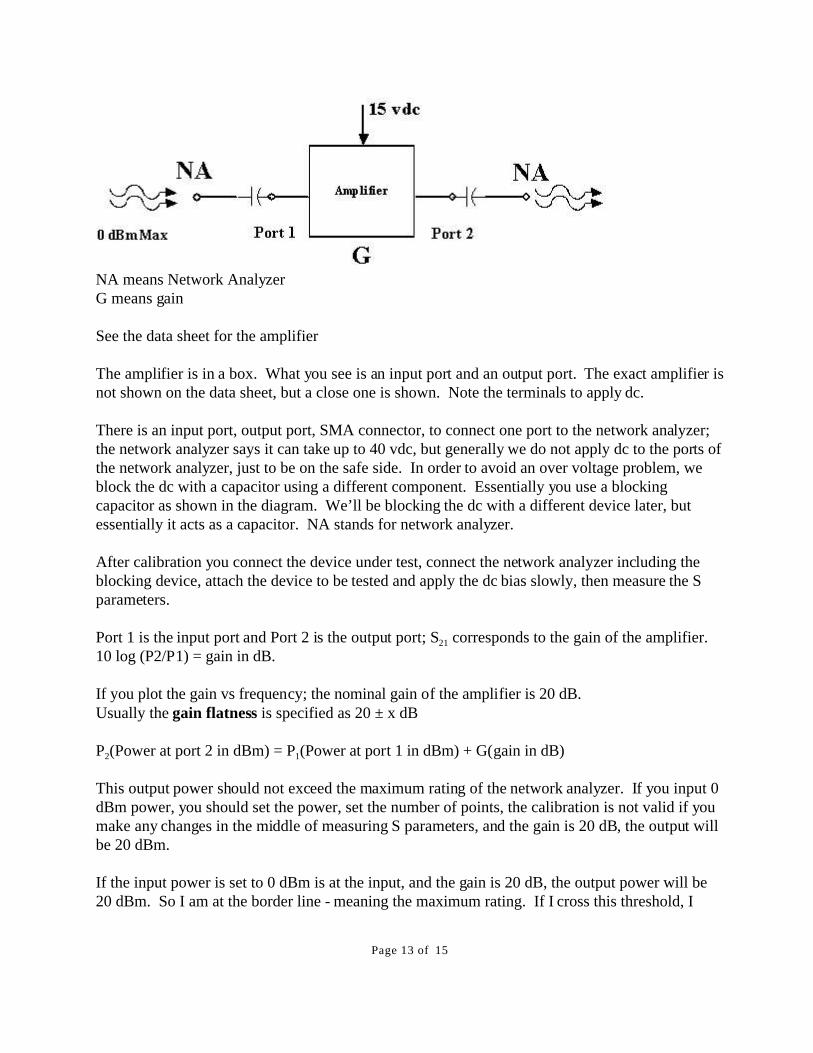
NA means Network AnalyzerG means gain
See the data sheet for the amplifier
The amplifier is in a box. What you see is an input port and an output port. The exact amplifier isnot shown on the data sheet, but a close one is shown. Note the terminals to apply dc.
There is an input port, output port, SMA connector, to connect one port to the network analyzer;the network analyzer says it can take up to 40 vdc, but generally we do not apply dc to the ports ofthe network analyzer, just to be on the safe side. In order to avoid an over voltage problem, weblock the dc with a capacitor using a different component. Essentially you use a blockingcapacitor as shown in the diagram. We’ll be blocking the dc with a different device later, butessentially it acts as a capacitor. NA stands for network analyzer.
After calibration you connect the device under test, connect the network analyzer including theblocking device, attach the device to be tested and apply the dc bias slowly, then measure the Sparameters.
Port 1 is the input port and Port 2 is the output port; S21 corresponds to the gain of the amplifier. 10 log (P2/P1) = gain in dB.
If you plot the gain vs frequency; the nominal gain of the amplifier is 20 dB.Usually the gain flatness is specified as 20 ± x dB
P2(Power at port 2 in dBm) = P1(Power at port 1 in dBm) + G(gain in dB)
This output power should not exceed the maximum rating of the network analyzer. If you input 0dBm power, you should set the power, set the number of points, the calibration is not valid if youmake any changes in the middle of measuring S parameters, and the gain is 20 dB, the output willbe 20 dBm.
If the input power is set to 0 dBm is at the input, and the gain is 20 dB, the output power will be20 dBm. So I am at the border line - meaning the maximum rating. If I cross this threshold, I
Page 14 of 15
don’t know what will happen. To be on the safe side, I can adjust the input power to - 10 dBm or-20 dBm so there is no chance of exceeding the maximum input power of 20 dBm.
The gain is independent of the power input to the device, since we are operating in the linearregion of the device.
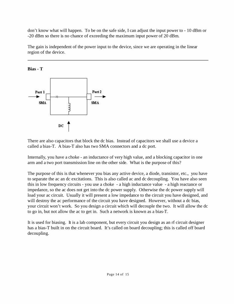
Bias - T
There are also capacitors that block the dc bias. Instead of capacitors we shall use a device acalled a bias-T. A bias-T also has two SMA connectors and a dc port.
Internally, you have a choke - an inductance of very high value, and a blocking capacitor in onearm and a two port transmission line on the other side. What is the purpose of this?
The purpose of this is that whenever you bias any active device, a diode, transistor, etc., you haveto separate the ac an dc excitations. This is also called ac and dc decoupling. You have also seenthis in low frequency circuits - you use a choke - a high inductance value - a high reactance orimpedance, so the ac does not get into the dc power supply. Otherwise the dc power supply willload your ac circuit. Usually it will present a low impedance to the circuit you have designed, andwill destroy the ac performance of the circuit you have designed. However, without a dc bias,your circuit won’t work. So you design a circuit which will decouple the two. It will allow the dcto go in, but not allow the ac to get in. Such a network is known as a bias-T.
It is used for biasing. It is a lab component, but every circuit you design as an rf circuit designerhas a bias-T built in on the circuit board. It’s called on board decoupling; this is called off boarddecoupling.
Page 15 of 15
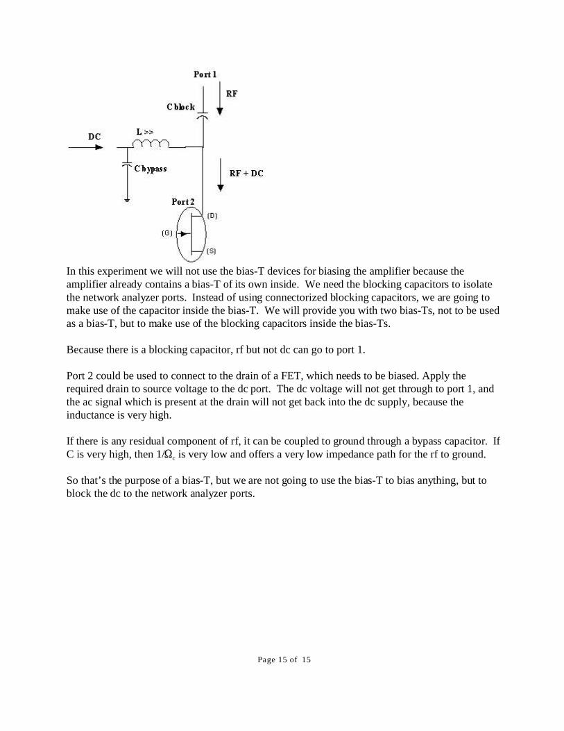
In this experiment we will not use the bias-T devices for biasing the amplifier because theamplifier already contains a bias-T of its own inside. We need the blocking capacitors to isolatethe network analyzer ports. Instead of using connectorized blocking capacitors, we are going tomake use of the capacitor inside the bias-T. We will provide you with two bias-Ts, not to be usedas a bias-T, but to make use of the blocking capacitors inside the bias-Ts.
Because there is a blocking capacitor, rf but not dc can go to port 1.
Port 2 could be used to connect to the drain of a FET, which needs to be biased. Apply therequired drain to source voltage to the dc port. The dc voltage will not get through to port 1, andthe ac signal which is present at the drain will not get back into the dc supply, because theinductance is very high.
If there is any residual component of rf, it can be coupled to ground through a bypass capacitor. IfC is very high, then 1/Sc is very low and offers a very low impedance path for the rf to ground.
So that’s the purpose of a bias-T, but we are not going to use the bias-T to bias anything, but toblock the dc to the network analyzer ports.