Embed Size (px)
Citation preview
©2004 Littelfuse, Inc. E1 - 1 http://www.littelfuse.comThyristor Product Catalog +1 972-580-7777
* Sele
cted P
ackages
U.L
. RECO
GNIZ
ED
File #
E7163
9
MT2 MT1
G
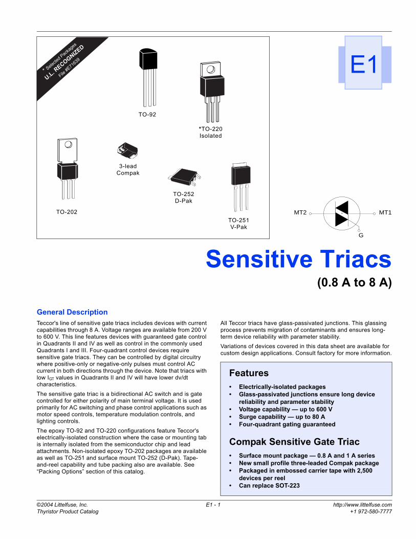
Sensitive Triacs(0.8 A to 8 A)
E1General DescriptionTeccor's line of sensitive gate triacs includes devices with current capabilities through 8 A. Voltage ranges are available from 200 V to 600 V. This line features devices with guaranteed gate control in Quadrants II and IV as well as control in the commonly used Quadrants I and III. Four-quadrant control devices require sensitive gate triacs. They can be controlled by digital circuitry where positive-only or negative-only pulses must control AC current in both directions through the device. Note that triacs with low IGT values in Quadrants II and IV will have lower dv/dt characteristics.The sensitive gate triac is a bidirectional AC switch and is gate controlled for either polarity of main terminal voltage. It is used primarily for AC switching and phase control applications such as motor speed controls, temperature modulation controls, and lighting controls.The epoxy TO-92 and TO-220 configurations feature Teccor's electrically-isolated construction where the case or mounting tab is internally isolated from the semiconductor chip and lead attachments. Non-isolated epoxy TO-202 packages are available as well as TO-251 and surface mount TO-252 (D-Pak). Tape-and-reel capability and tube packing also are available. See “Packing Options” section of this catalog.
All Teccor triacs have glass-passivated junctions. This glassing process prevents migration of contaminants and ensures long-term device reliability with parameter stability.Variations of devices covered in this data sheet are available for custom design applications. Consult factory for more information.
Features• Electrically-isolated packages• Glass-passivated junctions ensure long device
reliability and parameter stability• Voltage capability — up to 600 V• Surge capability — up to 80 A• Four-quadrant gating guaranteed
Compak Sensitive Gate Triac• Surface mount package — 0.8 A and 1 A series• New small profile three-leaded Compak package• Packaged in embossed carrier tape with 2,500
devices per reel• Can replace SOT-223
TO-202
TO-92
3-leadCompak
*TO-220Isolated
E1
TO-252D-Pak
TO-251V-Pak
Sensitive Triacs Data Sheets
http://www.littelfuse.com E1 - 2 ©2004 Littelfuse, Inc.+1 972-580-7777 Thyristor Product Catalog
See “General Notes” on page E1 - 4 and “Electrical Specification Notes” on page E1 - 5.
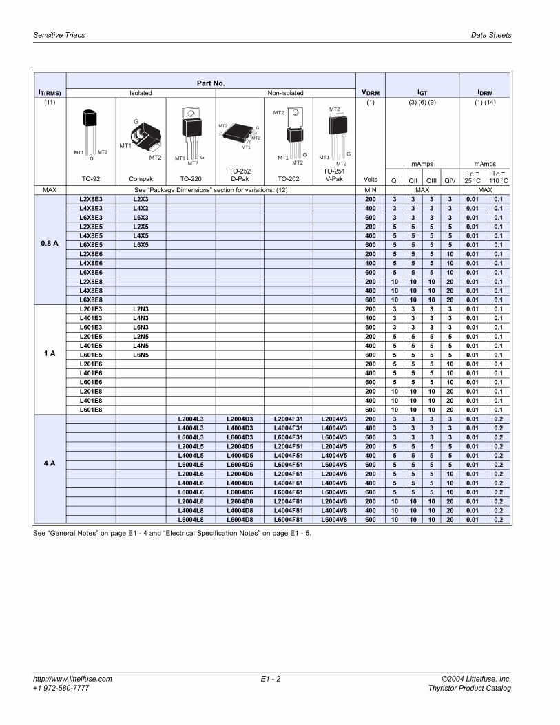
IT(RMS)Part No.
VDRM IGT IDRMIsolated Non-isolated(11)
TO-92 Compak TO-220TO-252D-Pak TO-202
TO-251V-Pak
(1)
Volts
(3) (6) (9)
mAmps
(1) (14)
mAmps
QI QII QIII QIVTC = 25 °C
TC = 110 °C
MAX See “Package Dimensions” section for variations. (12) MIN MAX MAX
0.8 A
L2X8E3 L2X3 200 3 3 3 3 0.01 0.1L4X8E3 L4X3 400 3 3 3 3 0.01 0.1L6X8E3 L6X3 600 3 3 3 3 0.01 0.1L2X8E5 L2X5 200 5 5 5 5 0.01 0.1L4X8E5 L4X5 400 5 5 5 5 0.01 0.1L6X8E5 L6X5 600 5 5 5 5 0.01 0.1L2X8E6 200 5 5 5 10 0.01 0.1L4X8E6 400 5 5 5 10 0.01 0.1L6X8E6 600 5 5 5 10 0.01 0.1L2X8E8 200 10 10 10 20 0.01 0.1L4X8E8 400 10 10 10 20 0.01 0.1L6X8E8 600 10 10 10 20 0.01 0.1
1 A
L201E3 L2N3 200 3 3 3 3 0.01 0.1L401E3 L4N3 400 3 3 3 3 0.01 0.1L601E3 L6N3 600 3 3 3 3 0.01 0.1L201E5 L2N5 200 5 5 5 5 0.01 0.1L401E5 L4N5 400 5 5 5 5 0.01 0.1L601E5 L6N5 600 5 5 5 5 0.01 0.1L201E6 200 5 5 5 10 0.01 0.1L401E6 400 5 5 5 10 0.01 0.1L601E6 600 5 5 5 10 0.01 0.1L201E8 200 10 10 10 20 0.01 0.1L401E8 400 10 10 10 20 0.01 0.1L601E8 600 10 10 10 20 0.01 0.1
4 A
L2004L3 L2004D3 L2004F31 L2004V3 200 3 3 3 3 0.01 0.2L4004L3 L4004D3 L4004F31 L4004V3 400 3 3 3 3 0.01 0.2L6004L3 L6004D3 L6004F31 L6004V3 600 3 3 3 3 0.01 0.2L2004L5 L2004D5 L2004F51 L2004V5 200 5 5 5 5 0.01 0.2L4004L5 L4004D5 L4004F51 L4004V5 400 5 5 5 5 0.01 0.2L6004L5 L6004D5 L6004F51 L6004V5 600 5 5 5 5 0.01 0.2L2004L6 L2004D6 L2004F61 L2004V6 200 5 5 5 10 0.01 0.2L4004L6 L4004D6 L4004F61 L4004V6 400 5 5 5 10 0.01 0.2L6004L6 L6004D6 L6004F61 L6004V6 600 5 5 5 10 0.01 0.2L2004L8 L2004D8 L2004F81 L2004V8 200 10 10 10 20 0.01 0.2L4004L8 L4004D8 L4004F81 L4004V8 400 10 10 10 20 0.01 0.2L6004L8 L6004D8 L6004F81 L6004V8 600 10 10 10 20 0.01 0.2
MT1G
MT2
G
MT1
MT2 MT1MT2
G
MT2
MT2
MT1
G
MT1 G
MT2
MT2MT2
MT2
GMT1
Data Sheets Sensitive Triacs
©2004 Littelfuse, Inc. E1 - 3 http://www.littelfuse.comThyristor Product Catalog +1 972-580-7777
See “General Notes” on page E1 - 4 and “Electrical Specification Notes” on page E1 - 5.
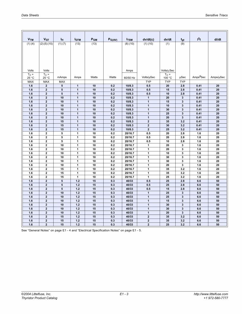
VTM VGT IH IGTM PGM PG(AV) ITSM dv/dt(c) dv/dt tgt I2t di/dt(1) (4)
Volts
(2) (5) (15)
Volts
(1) (7)
mAmps
(13)
Amps
(13)
Watts Watts
(8) (10)
Amps
(1) (10)
Volts/µSec
(1)
Volts/µSec
(9)
µSec Amps2Sec Amps/µSecTC = 25 °C
TC = 25 °C 60/50 Hz
TC = 100 °C
MAX MAX MAX TYP TYP TYP1.6 2 5 1 10 0.2 10/8.3 0.5 20 2.8 0.41 201.6 2 5 1 10 0.2 10/8.3 0.5 15 2.8 0.41 201.6 2 5 1 10 0.2 10/8.3 0.5 10 2.8 0.41 201.6 2 10 1 10 0.2 10/8.3 1 20 3 0.41 201.6 2 10 1 10 0.2 10/8.3 1 15 3 0.41 201.6 2 10 1 10 0.2 10/8.3 1 10 3 0.41 201.6 2 10 1 10 0.2 10/8.3 1 30 3 0.41 201.6 2 10 1 10 0.2 10/8.3 1 25 3 0.41 201.6 2 10 1 10 0.2 10/8.3 1 20 3 0.41 201.6 2 15 1 10 0.2 10/8.3 2 35 3.2 0.41 201.6 2 15 1 10 0.2 10/8.3 2 30 3.2 0.41 201.6 2 15 1 10 0.2 10/8.3 2 25 3.2 0.41 201.6 2 5 1 10 0.2 20/16.7 0.5 20 2.8 1.6 201.6 2 5 1 10 0.2 20/16.7 0.5 20 2.8 1.6 201.6 2 5 1 10 0.2 20/16.7 0.5 10 2.8 1.6 201.6 2 10 1 10 0.2 20/16.7 1 20 3 1.6 201.6 2 10 1 10 0.2 20/16.7 1 20 3 1.6 201.6 2 10 1 10 0.2 20/16.7 1 10 3 1.6 201.6 2 10 1 10 0.2 20/16.7 1 30 3 1.6 201.6 2 10 1 10 0.2 20/16.7 1 30 3 1.6 201.6 2 10 1 10 0.2 20/16.7 1 20 3 1.6 201.6 2 15 1 10 0.2 20/16.7 1 35 3.2 1.6 201.6 2 15 1 10 0.2 20/16.7 1 35 3.2 1.6 201.6 2 15 1 10 0.2 20/16.7 1 25 3.2 1.6 201.6 2 5 1.2 15 0.3 40/33 0.5 25 2.8 6.6 501.6 2 5 1.2 15 0.3 40/33 0.5 25 2.8 6.6 501.6 2 5 1.2 15 0.3 40/33 0.5 15 2.8 6.6 501.6 2 10 1.2 15 0.3 40/33 1 25 3 6.6 501.6 2 10 1.2 15 0.3 40/33 1 25 3 6.6 501.6 2 10 1.2 15 0.3 40/33 1 15 3 6.6 501.6 2 10 1.2 15 0.3 40/33 1 30 3 6.6 501.6 2 10 1.2 15 0.3 40/33 1 30 3 6.6 501.6 2 10 1.2 15 0.3 40/33 1 20 3 6.6 501.6 2 15 1.2 15 0.3 40/33 2 35 3.2 6.6 501.6 2 15 1.2 15 0.3 40/33 2 35 3.2 6.6 501.6 2 15 1.2 15 0.3 40/33 2 25 3.2 6.6 50
Sensitive Triacs Data Sheets
http://www.littelfuse.com E1 - 4 ©2004 Littelfuse, Inc.+1 972-580-7777 Thyristor Product Catalog
Specified Test Conditionsdi/dt — Maximum rate-of-change of on-state current; IGT = 50 mA with
0.1 µs rise timedv/dt — Critical rate-of-rise of off-state voltage at rated VDRM gate opendv/dt(c) — Critical rate-of-rise of commutation voltage at rated VDRM
and IT(RMS) commutating di/dt = 0.54 rated IT(RMS)/ms; gate unenergized
I2t — RMS surge (non-repetitive) on-state current for period of 8.3 ms for fusing
IDRM — Peak off-state current, gate open; VDRM = max rated valueIGT — DC gate trigger current in specific operating quadrants;
VD = 12 V dc; RL = 60 Ω
IGTM — Peak gate trigger currentIH — Holding current gate open; initial on-state current = 100 mA dcIT(RMS) — RMS on-state current conduction angle of 360°ITSM — Peak one-cycle surgePG(AV) — Average gate power dissipationPGM — Peak gate power dissipation; IGT ≤ IGTM
tgt — Gate controlled turn-on time; IGT = 50 mA with 0.1 µs rise timeVDRM — Repetitive peak off-state/blocking voltageVGT — DC gate trigger voltage; VD = 12 V dc; RL = 60 Ω
VTM — Peak on-state voltage at max rated RMS current
General Notes• All measurements are made with 60 Hz resistive load and at an
ambient temperature of +25 °C unless otherwise specified.• Operating temperature range (TJ) is -65 °C to +110 °C for TO-92
devices and -40 °C to +110 °C for all other devices.• Storage temperature range (TS) is -65 °C to +150 °C for TO-92
devices, -40 °C to +150 °C for TO-202 devices, and -40 °C to +125 °C for TO-220 devices.
• Lead solder temperature is a maximum of 230 °C for 10 seconds maximum at a minimum of 1/16” (1.59 mm) from case.
• The case or lead temperature (TC or TL) is measured as shown on dimensional outline drawings. See “Package Dimensions” section of this catalog.
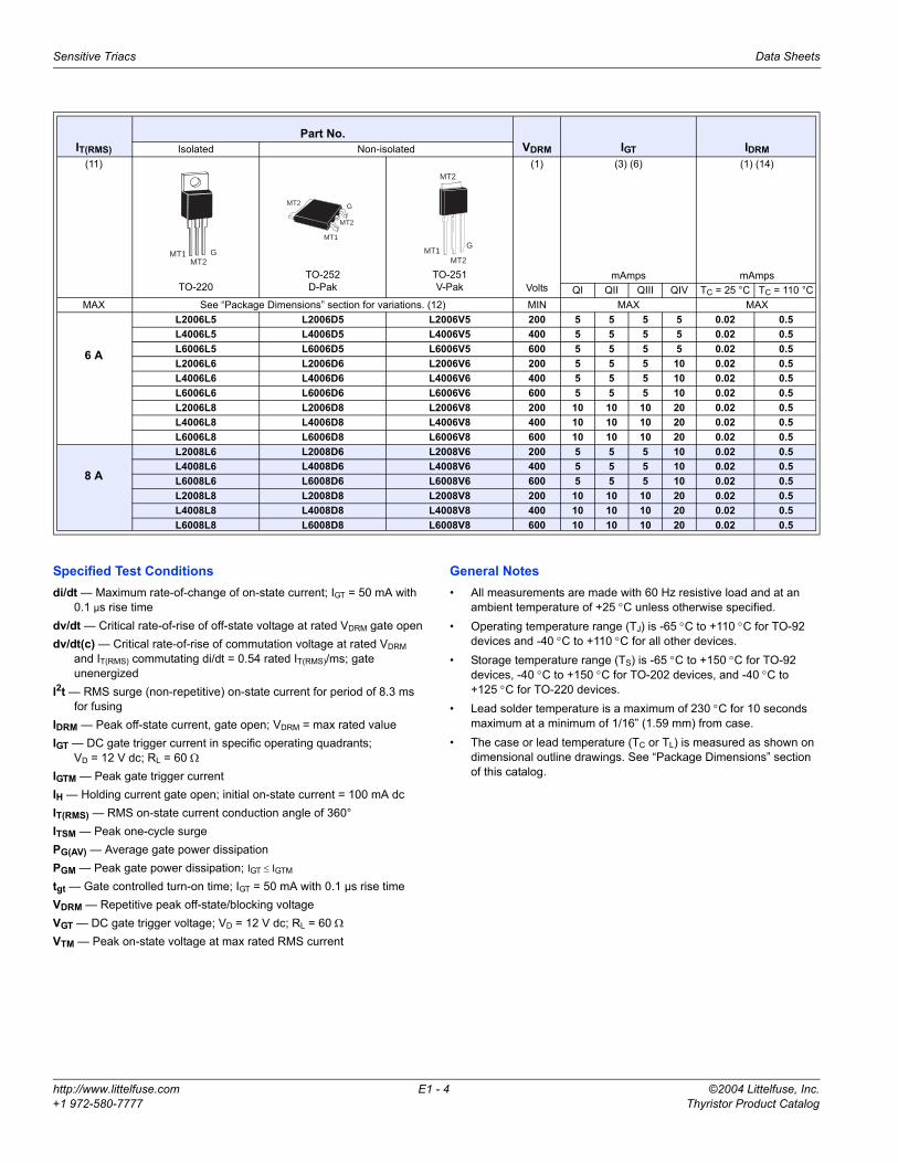
IT(RMS)Part No.
VDRM IGT IDRMIsolated Non-isolated(11)
TO-220TO-252D-Pak
TO-251V-Pak
(1)
Volts
(3) (6)
mAmps
(1) (14)
mAmpsQI QII QIII QIV TC = 25 °C TC = 110 °C
MAX See “Package Dimensions” section for variations. (12) MIN MAX MAX
6 A
L2006L5 L2006D5 L2006V5 200 5 5 5 5 0.02 0.5L4006L5 L4006D5 L4006V5 400 5 5 5 5 0.02 0.5L6006L5 L6006D5 L6006V5 600 5 5 5 5 0.02 0.5L2006L6 L2006D6 L2006V6 200 5 5 5 10 0.02 0.5L4006L6 L4006D6 L4006V6 400 5 5 5 10 0.02 0.5L6006L6 L6006D6 L6006V6 600 5 5 5 10 0.02 0.5L2006L8 L2006D8 L2006V8 200 10 10 10 20 0.02 0.5L4006L8 L4006D8 L4006V8 400 10 10 10 20 0.02 0.5L6006L8 L6006D8 L6006V8 600 10 10 10 20 0.02 0.5
8 A
L2008L6 L2008D6 L2008V6 200 5 5 5 10 0.02 0.5L4008L6 L4008D6 L4008V6 400 5 5 5 10 0.02 0.5L6008L6 L6008D6 L6008V6 600 5 5 5 10 0.02 0.5L2008L8 L2008D8 L2008V8 200 10 10 10 20 0.02 0.5L4008L8 L4008D8 L4008V8 400 10 10 10 20 0.02 0.5L6008L8 L6008D8 L6008V8 600 10 10 10 20 0.02 0.5
MT1MT2
G
MT2
MT2
MT1
G
MT2
MT2
GMT1

Data Sheets Sensitive Triacs
©2004 Littelfuse, Inc. E1 - 5 http://www.littelfuse.comThyristor Product Catalog +1 972-580-7777
Electrical Specification Notes (1) For either polarity of MT2 with reference to MT1 terminal(2) For either polarity of gate voltage VGT with reference to MT1
terminal(3) See Gate Characteristics and Definition of Quadrants.(4) See Figure E1.4 for iT versus vT.(5) See Figure E1.6 for VGT versus TC.(6) See Figure E1.7 for IGT versus TC.(7) See Figure E1.5 for IH versus TC.(8) See Figure E1.9 for surge rating and specific duration.(9) See Figure E1.8 for tgt versus IGT.(10) See Figure E1.2 and Figure E1.3 for maximum allowable case
temperature at maximum rated current.(11) See Figure E1.1, Figure E1.2, and Figure E1.3 for TA or TC versus
IT(RMS).(12) See package outlines for lead form configurations. When ordering
special lead forming, add type number as suffix to part number.(13) Pulse width ≤10 µs(14) TC or TL = TJ for test conditions in off state(15) Minimum non-trigger VGT at 110 °C is 0.2 V.
Gate CharacteristicsTeccor triacs may be turned on between gate and MT1 terminals in the following ways:• In-phase signals (with standard AC line) using Quadrants I
and III• Application of unipolar pulses (gate always positive or nega-
tive), using Quadrants II and III with negative gate pulses and Quadrants I and IV with positive gate pulses
When maximum surge capability is required, pulses should be a minimum of one magnitude above IGT rating with a steep rising waveform (≤1 µs rise time).
Definition of Quadrants
VTM VGT IH IGTM PGM PG(AV) ITSM dv/dt(c) dv/dt tgt I2t di/dt(1) (4)
Volts
(2) (5) (15)
Volts
(1) (7)
mAmps
(13)
Amps
(13)
Watts Watts
(8) (10)
Amps
(1) (10)
Volts/µSec
(1)
Volts/µSec
(9)
µSec Amps2Sec Amps/µSecTC = 25 °C TC = 25 °C 60/50 Hz TC = 100 °CMAX MAX MAX TYP TYP TYP1.6 2 10 1.6 18 0.4 60/50 1 40 3 15 701.6 2 10 1.6 18 0.4 60/50 1 30 3 15 701.6 2 10 1.6 18 0.4 60/50 1 20 3 15 701.6 2 10 1.6 18 0.4 60/50 2 40 3 15 701.6 2 10 1.6 18 0.4 60/50 2 30 3 15 701.6 2 10 1.6 18 0.4 60/50 2 20 3 15 701.6 2 20 1.6 18 0.4 60/50 2 45 3.2 15 701.6 2 20 1.6 18 0.4 60/50 2 40 3.2 15 701.6 2 20 1.6 18 0.4 60/50 2 30 3.2 15 701.6 2 10 1.6 18 0.4 80/65 2 40 3 26.5 701.6 2 10 1.6 18 0.4 80/65 2 30 3 26.5 701.6 2 10 1.6 18 0.4 80/65 2 20 3 26.5 701.6 2 20 1.6 18 0.4 80/65 2 45 3.2 26.5 701.6 2 20 1.6 18 0.4 80/65 2 40 3.2 26.5 701.6 2 20 1.6 18 0.4 80/65 2 30 3.2 26.5 70
MT2 POSITIVE(Positive Half Cycle)
MT2 NEGATIVE(Negative Half Cycle)
MT1
MT2
+ I G T
REFQII
MT1
I G TGATE
MT2
REF
MT1
MT2
REF
MT1
MT2
REF
QIQIV QIII
ALL POLARITIES ARE REFERENCED TO MT1
(-)
I G TGATE
(+)
I G T -
I G TGATE
(-)
I G TGATE
(+)
+
-

Sensitive Triacs Data Sheets
http://www.littelfuse.com E1 - 6 ©2004 Littelfuse, Inc.+1 972-580-7777 Thyristor Product Catalog
Electrical IsolationTeccor’s isolated triac packages withstand a minimum high potential test of 2500 V ac rms from leads to mounting tab over the device's operating temperature range. The following isolation table shows standard isolation ratings.
*UL Recognized File #E71639
* Mounted on 1 cm2 copper foil surface; two-ounce copper foil
Figure E1.1 Maximum Allowable Ambient Temperature versusOn-state Current
Figure E1.2 Maximum Allowable Case Temperature versusOn-state Current (0.8 A and 1 A)
Electrical Isolationfrom Leads to Mounting Tab
V AC RMS TO-220 *2500 Standard
Thermal Resistance (Steady State) Junction to Mounting Taband Junction to AmbientRθJC [RθJA] °C/W (TYP)
Package Code E C F L F2 D V
Type
TO-92Plastic Compak
TO-202Type 1
TO-220Isolated
TO-202Type 2
TO-252D-Pak
TO-251V-Pak
0.8 A 60 [135] 60 *1 A 50 [95] 40 *4 A 3.5 [45] 3.6 [50] 6.0 [70] 3.5 6.0 [70]6 A 3.3 3.2 3.28 A 2.8 2.7 2.7
20
40
60
80
100
120
RMS On-State Current [IT(RMS)] - Amps
Max
imum
Allo
wab
le A
mbi
ent T
empe
ratu
re (
TA)
- ˚C CURRENT WAVEFORM: Sinusoidal
LOAD: Resistive or InductiveCONDUCTION ANGLE: 360˚ FREE AIR RATING – NO HEATSINK
TO-220 andTYPE 1 and 3 TO-202
TYPE 2 and 4 TO-202and TO-251
0.8 A TO-92
1 A TO-92
25
0 0.2 0.4 0.6 0.8 1.0 1.2 1.4 1.6 1.80 0.2 0.4 0.6 0.8 1.0 1.2 1.4 1.6
50
60
70
80
90
100
110
Max
imum
Allo
wab
le C
ase
Tem
pera
ture
(T
C)
– ˚C
CURRENT WAVEFORM: SinusoidalLOAD: Resistive or InductiveCONDUCTION ANGLE: 360˚CASE TEMPERATURE: Measured asshown on Dimensional Drawings
RMS On-State Current [IT(RMS)] – Amps
1 A
0.8 A

Data Sheets Sensitive Triacs
©2004 Littelfuse, Inc. E1 - 7 http://www.littelfuse.comThyristor Product Catalog +1 972-580-7777
Figure E1.3 Maximum Allowable Case Temperature versusOn-state Current (4 A, 6 A, and 8 A)
Figure E1.4 On-state Current versus On-state Voltage (Typical)
Figure E1.5 Normalized DC Holding Current versus Case Temperature
Figure E1.6 Normalized DC Gate Trigger Voltage for All Quadrants versus Case Temperature
Figure E1.7 Normalized DC Gate Trigger Current for All Quadrants versus Case Temperature
Figure E1.8 Turn-on Time versus Gate Trigger Current (Typical)
0 1 2 3 4 5 6 7 8
60
65
70
75
80
85
90
95
100
105
110
RMS On-State Current [IT(RMS)] - Amps
Max
imum
Allo
wab
le C
ase
Tem
pera
ture
(T
C)
- ˚C
CURRENT WAVEFORM: SinusoidalLOAD: Resistive or Inductive
CONDUCTION ANGLE: 360˚CASE TEMPERATURE: Measured asshown on Dimensional Drawings
4 A TYPE 1 and 3 TO-2024 A TO-220 (Isolated)4 A TO-252
8 A TO-220 (Isolated)
6 A TO-220 (Isolated)
4 A TYPE 2 and 4 TO-2024 A TO-251
8 A TO-251 and TO-252
6 A TO-2516 A TO-252
0 0.5 0.8 1.0 1.2 1.4 1.6 1.8
0
2
4
6
8
10
12
14
16
18
20
Positive or Negative InstantaneousOn-state Voltage (vT) - Volts
Pos
itive
or
Neg
ativ
e In
stan
tane
ous
On-
stat
e C
urre
nt (
i T)
- A
mps
1 A
4 A
6 A and 8 A
TC = 25 ˚C
0.8 A
-40 -15 +25 +65 +110 +125
0
1.0
2.0
3.0
4.0
-65
Case Temperature (TC) - C
INITIAL ON-STATE CURRENT = 100 mA (DC) 0.8 - 4 A Devices= 200 mA (DC) 6 - 8 A Devices
Rat
io o
fI H
I H (
TC
= 2
5 C
)
-65 -40 -15 +65 +110+125+25
0
.5
1.0
1.5
2.0
Rat
io o
fV
GT
VG
T (
TC
= 2
5 ˚C
)
Case Temperature (TC) - ˚ C
-65 -40 -15 +65 +110+125+25
0
1.0
2.0
3.0
4.0
Rat
io o
fI G
T
I GT (
TC
= 2
5 ˚C
)
Case Temperature (TC) - ˚C
1 2 3 4 65 8 10 20 30 40 60 80 100
IGT = 5 mA MAX
IGT = 10 mA MAX
IGT = 20 mA MAX
IGT = 3 mA MAX
0
1.0
2.0
3.0
4.0
5.0
6.0
7.0
DC Gate Trigger Current (IGT) - mA
Tur
n-O
n T
ime
(tgt
) -
µSec
TC = 25 ˚C

Sensitive Triacs Data Sheets
http://www.littelfuse.com E1 - 8 ©2004 Littelfuse, Inc.+1 972-580-7777 Thyristor Product Catalog
Figure E1.9 Peak Surge Current versus Surge Current Duration
Figure E1.10 Power Dissipation (Typical) versus RMS On-state Current(0.8 A and 1 A)
Figure E1.11 Power Dissipation (Typical) versus RMS On-state Current(4 A, 6 A, and 8 A)
1 2 43 6 8 10 20 4030 60 100 200 400 600 1000
1
2
34
6
108
20
30
40
60
10080
150
200
Surge Current Duration – Full Cycles
Pea
k S
urge
(N
on-R
epet
itive
)O
n-S
tate
Cur
rent
(I T
SM
) –
Am
ps
8 A
6 A
0.8 A
SUPPLY FREQUENCY: 60 Hz SinusoidalLOAD: ResistiveRMS On-state Current: [IT(RMS)]: Maximum Rated Value at Specified Case Temperature
NOTES:1) Gate control may be lost duringand immediately following surgecurrent interval.2) Overload may not be repeated untiljunction temperature has returnedto steady-state rated value.
1 A
4 A
0 0.25 0.50 0.75 1.0 1.25 1.5
0
0.5
1.0
1.5
RMS On-state Current [IT(RMS)] – Amps
Ave
rage
On-
stat
e P
ower
Dis
sipa
tion
[PD
(AV
)] –
Wat
ts
CURRENT WAVEFORM: SinusoidalLOAD: Resistive or InductiveCONDUCTION ANGLE: 360˚
1 A0.8 A
0 .5 1.0 1.5 2.0 2.5 3.0 3.5 4.0 4.5 5.0 5.5 6.0 6.5 7.0 7.5
0
1.0
2.0
3.0
4.0
5.0
6.0
7.0
8.0
9.0
8.0
6 A and 8 A
4 A
RMS On-state Current [IT(RMS)] – Amps
Aver
age
On-
stat
e Po
wer
Dis
sipa
tion
[PD
(AV)
] – W
atts
CURRENT WAVEFORM: SinusoidalLOAD: Resistive or InductiveCONDUCTION ANGLE: 360˚

©2004 Littelfuse, Inc. E2 - 1 http://www.littelfuse.comThyristor Product Catalog +1 972-580-7777
* Selecte
d Pack
ages
U.L
. RECO
GNIZ
ED
File #E
7163
9
Triacs(0.8 A to 35 A)
E2General DescriptionThese gated triacs from Teccor Electronics are part of a broad line of bidirectional semiconductors. The devices range in current ratings from 0.8 A to 35 A and in voltages from 200 V to 1000 V.The triac may be gate triggered from a blocking to conduction state for either polarity of applied voltage and is designed for AC switching and phase control applications such as speed and tem-perature modulation controls, lighting controls, and static switch-ing relays. The triggering signal is normally applied between the gate and MT1.Isolated packages are offered with internal construction, having the case or mounting tab electrically isolated from the semicon-ductor chip. This feature facilitates the use of low-cost assembly and convenient packaging techniques. Tape-and-reel capability is available. See “Packing Options” section of this catalog.All Teccor triacs have glass-passivated junctions to ensure long-term device reliability and parameter stability. Teccor's glass-passivated junctions offer a rugged, reliable barrier against junc-tion contamination.
Variations of devices covered in this data sheet are available for custom design applications. Consult factory for more information.
Features• Electrically-isolated packages• Glass-passivated junctions• Voltage capability — up to 1000 V• Surge capability — up to 200 A
Compak Package• Surface mount package — 0.8 A and 1 A series• New small profile three-leaded Compak package• Packaged in embossed carrier tape with 2,500
devices per reel• Can replace SOT-223
E2
MT2 MT1
G
*TO-220
3-leadCompak
TO-92
TO-251V-Pak
TO-263D2Pak
TO-92
TO-252D-Pak
*TO-3Fastpak
TO-202
Triacs Data Sheets
http://www.littelfuse.com E2 - 2 ©2004 Littelfuse, Inc.+1 972-580-7777 Thyristor Product Catalog
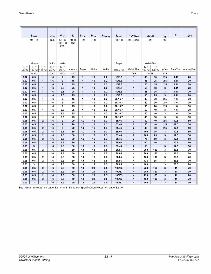
See “General Notes” on page E2 - 4 and “Electrical Specification Notes” on page E2 - 5.
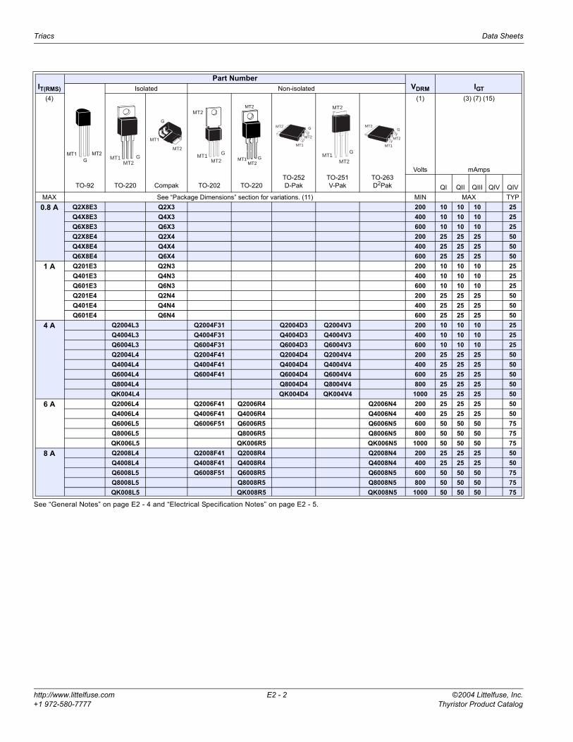
IT(RMS)
Part NumberVDRM IGTIsolated Non-isolated
(4)
TO-92 TO-220 Compak TO-202 TO-220TO-252D-Pak
TO-251V-Pak
TO-263D2Pak
(1)
Volts
(3) (7) (15)
mAmps
QI QII QIII QIV QIVMAX See “Package Dimensions” section for variations. (11) MIN MAX TYP0.8 A Q2X8E3 Q2X3 200 10 10 10 25
Q4X8E3 Q4X3 400 10 10 10 25Q6X8E3 Q6X3 600 10 10 10 25Q2X8E4 Q2X4 200 25 25 25 50Q4X8E4 Q4X4 400 25 25 25 50Q6X8E4 Q6X4 600 25 25 25 50
1 A Q201E3 Q2N3 200 10 10 10 25Q401E3 Q4N3 400 10 10 10 25Q601E3 Q6N3 600 10 10 10 25Q201E4 Q2N4 200 25 25 25 50Q401E4 Q4N4 400 25 25 25 50Q601E4 Q6N4 600 25 25 25 50
4 A Q2004L3 Q2004F31 Q2004D3 Q2004V3 200 10 10 10 25Q4004L3 Q4004F31 Q4004D3 Q4004V3 400 10 10 10 25Q6004L3 Q6004F31 Q6004D3 Q6004V3 600 10 10 10 25Q2004L4 Q2004F41 Q2004D4 Q2004V4 200 25 25 25 50Q4004L4 Q4004F41 Q4004D4 Q4004V4 400 25 25 25 50Q6004L4 Q6004F41 Q6004D4 Q6004V4 600 25 25 25 50Q8004L4 Q8004D4 Q8004V4 800 25 25 25 50QK004L4 QK004D4 QK004V4 1000 25 25 25 50
6 A Q2006L4 Q2006F41 Q2006R4 Q2006N4 200 25 25 25 50Q4006L4 Q4006F41 Q4006R4 Q4006N4 400 25 25 25 50Q6006L5 Q6006F51 Q6006R5 Q6006N5 600 50 50 50 75Q8006L5 Q8006R5 Q8006N5 800 50 50 50 75QK006L5 QK006R5 QK006N5 1000 50 50 50 75
8 A Q2008L4 Q2008F41 Q2008R4 Q2008N4 200 25 25 25 50Q4008L4 Q4008F41 Q4008R4 Q4008N4 400 25 25 25 50Q6008L5 Q6008F51 Q6008R5 Q6008N5 600 50 50 50 75Q8008L5 Q8008R5 Q8008N5 800 50 50 50 75QK008L5 QK008R5 QK008N5 1000 50 50 50 75
MT1G
MT2MT1
MT2G
G
MT1
MT2
MT1 G
MT2
MT2
MT1 GMT2
MT2
MT2
MT2
MT1
G
MT2
MT2
GMT1
MT2
MT2
MT1
G
Data Sheets Triacs
©2004 Littelfuse, Inc. E2 - 3 http://www.littelfuse.comThyristor Product Catalog +1 972-580-7777
See “General Notes” on page E2 - 4 and “Electrical Specification Notes” on page E2 - 5.
IDRM VTM VGT IH IGTM PGM PG(AV) ITSM dv/dt(c) dv/dt tgt I2t di/dt(1) (16)
mAmps
(1) (5)
Volts
(2) (6) (15) (18)
(19)
Volts
(1) (8) (12)
mAmps
(14)
Amps
(14)
Watts Watts
(9) (13)
Amps
(1) (4) (13)
Volts/µSec
(1)
Volts/µSec
(10)
µSec Amp2Sec Amps/µSecTC =25 °C
TC =100 °C
TC =125 °C
TC =25 °C
TC =25 °C 60/50 Hz
TC=100 °C
TC=125 °C
MAX MAX MAX MAX TYP MIN TYP0.02 0.5 1 1.6 2 15 1 10 0.2 10/8.3 1 40 30 2.5 0.41 200.02 0.5 1 1.6 2 15 1 10 0.2 10/8.3 1 35 25 2.5 0.41 200.02 0.5 1 1.6 2 15 1 10 0.2 10/8.3 1 25 15 2.5 0.41 200.02 0.5 1 1.6 2.5 25 1 10 0.2 10/8.3 1 50 40 3 0.41 200.02 0.5 1 1.6 2.5 25 1 10 0.2 10/8.3 1 45 35 3 0.41 200.02 0.5 1 1.6 2.5 25 1 10 0.2 10/8.3 1 35 25 3 0.41 200.02 0.5 1 1.6 2 15 1 10 0.2 20/16.7 1 40 30 2.5 1.6 300.02 0.5 1 1.6 2 15 1 10 0.2 20/16.7 1 40 30 2.5 1.6 300.02 0.5 1 1.6 2 15 1 10 0.2 20/16.7 1 30 20 2.5 1.6 300.02 0.5 1 1.6 2.5 25 1 10 0.2 20/16.7 1 50 40 3 1.6 300.02 0.5 1 1.6 2.5 25 1 10 0.2 20/16.7 1 50 40 3 1.6 300.02 0.5 1 1.6 2.5 25 1 10 0.2 20/16.7 1 40 30 3 1.6 300.05 0.5 2 1.6 2 20 1.2 15 0.3 55/46 2 50 40 2.5 12.5 500.05 0.5 2 1.6 2 20 1.2 15 0.3 55/46 2 50 40 2.5 12.5 500.05 0.5 2 1.6 2 20 1.2 15 0.3 55/46 2 40 30 2.5 12.5 500.05 0.5 2 1.6 2.5 30 1.2 15 0.3 55/46 2 100 75 3 12.5 500.05 0.5 2 1.6 2.5 30 1.2 15 0.3 55/46 2 100 75 3 12.5 500.05 0.5 2 1.6 2.5 30 1.2 15 0.3 55/46 2 75 50 3 12.5 500.05 0.5 2 1.6 2.5 30 1.2 15 0.3 55/46 2 60 40 3 12.5 500.05 3 1.6 2.5 30 1.2 15 0.3 55/46 2 50 3 12.5 500.05 0.5 2 1.6 2.5 50 1.6 18 0.5 80/65 4 200 120 3 26.5 700.05 0.5 2 1.6 2.5 50 1.6 18 0.5 80/65 4 200 120 3 26.5 700.05 0.5 2 1.6 2.5 50 1.6 18 0.5 80/65 4 150 100 3 26.5 700.05 0.5 2 1.6 2.5 50 1.6 18 0.5 80/65 4 125 85 3 26.5 700.05 3 1.6 2.5 50 1.6 18 0.5 80/65 4 100 3 26.5 700.05 0.5 2 1.6 2.5 50 1.8 20 0.5 100/83 4 250 150 3 41 700.05 0.5 2 1.6 2.5 50 1.8 20 0.5 100/83 4 250 150 3 41 700.05 0.5 2 1.6 2.5 50 1.8 20 0.5 100/83 4 220 125 3 41 700.05 0.5 2 1.6 2.5 50 1.8 20 0.5 100/83 4 150 100 3 41 700.05 3 1.6 2.5 50 1.8 20 0.5 100/83 4 100 3 41 70
Triacs Data Sheets
http://www.littelfuse.com E2 - 4 ©2004 Littelfuse, Inc.+1 972-580-7777 Thyristor Product Catalog
Specific Test Conditionsdi/dt — Maximum rate-of-change of on-state current; IGT = 200 mA with
≤0.1 µs rise timedv/dt — Critical rate-of-rise of off-state voltage at rated VDRM gate opendv/dt(c) — Critical rate-of-rise of commutation voltage at rated VDRM
and IT(RMS) commutating di/dt = 0.54 rated IT(RMS)/ms; gate unenergized
I2t — RMS surge (non-repetitive) on-state current for period of 8.3 ms for fusing
IDRM — Peak off-state current, gate open; VDRM = maximum rated valueIGT — DC gate trigger current in specific operating quadrants;
VD = 12 V dcIGTM — Peak gate trigger currentIH — Holding current (DC); gate openIT(RMS) — RMS on-state current conduction angle of 360°ITSM — Peak one-cycle surgePG(AV) — Average gate power dissipationPGM — Peak gate power dissipation; IGT ≤ IGTM
tgt — Gate controlled turn-on time; IGT = 200 mA with 0.1 µs rise time
VDRM — Repetitive peak blocking voltageVGT — DC gate trigger voltage; VD = 12 V dc; RL = 60 Ω
VTM — Peak on-state voltage at maximum rated RMS current
General Notes• All measurements are made at 60 Hz with a resistive load at an
ambient temperature of +25 °C unless specified otherwise.• Operating temperature range (TJ) is -65 °C to +125 °C for TO-92,
-25 °C to +125 °C for Fastpak, and -40 °C to +125 °C for all other devices.
• Storage temperature range (TS) is -65 °C to +150 °C for TO-92,-40 °C to +150 °C for TO-202, and -40 °C to +125 °C for all other devices.
• Lead solder temperature is a maximum of 230 °C for 10 seconds, maximum; ≥1/16" (1.59 mm) from case.
• The case temperature (TC) is measured as shown on the dimen-sional outline drawings. See “Package Dimensions” section of this catalog.
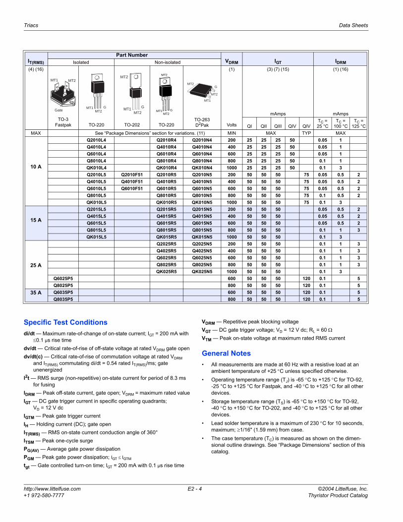
IT(RMS)
Part NumberVDRM IGT IDRMIsolated Non-isolated
(4) (16)
TO-3Fastpak TO-220 TO-202 TO-220
TO-263D2Pak
(1)
Volts
(3) (7) (15)
mAmps
(1) (16)
mAmps
QI QII QIII QIV QIVTC = 25 °C
TC = 100 °C
TC = 125 °C
MAX See “Package Dimensions” section for variations. (11) MIN MAX TYP MAX
10 A
Q2010L4 Q2010R4 Q2010N4 200 25 25 25 50 0.05 1Q4010L4 Q4010R4 Q4010N4 400 25 25 25 50 0.05 1Q6010L4 Q6010R4 Q6010N4 600 25 25 25 50 0.05 1Q8010L4 Q8010R4 Q8010N4 800 25 25 25 50 0.1 1QK010L4 QK010R4 QK010N4 1000 25 25 25 50 0.1 3Q2010L5 Q2010F51 Q2010R5 Q2010N5 200 50 50 50 75 0.05 0.5 2Q4010L5 Q4010F51 Q4010R5 Q4010N5 400 50 50 50 75 0.05 0.5 2Q6010L5 Q6010F51 Q6010R5 Q6010N5 600 50 50 50 75 0.05 0.5 2Q8010L5 Q8010R5 Q8010N5 800 50 50 50 75 0.1 0.5 2QK010L5 QK010R5 QK010N5 1000 50 50 50 75 0.1 3
15 A
Q2015L5 Q2015R5 Q2015N5 200 50 50 50 0.05 0.5 2Q4015L5 Q4015R5 Q4015N5 400 50 50 50 0.05 0.5 2Q6015L5 Q6015R5 Q6015N5 600 50 50 50 0.05 0.5 2Q8015L5 Q8015R5 Q8015N5 800 50 50 50 0.1 1 3QK015L5 QK015R5 QK015N5 1000 50 50 50 0.1 3
25 A
Q2025R5 Q2025N5 200 50 50 50 0.1 1 3Q4025R5 Q4025N5 400 50 50 50 0.1 1 3Q6025R5 Q6025N5 600 50 50 50 0.1 1 3Q8025R5 Q8025N5 800 50 50 50 0.1 1 3QK025R5 QK025N5 1000 50 50 50 0.1 3
Q6025P5 600 50 50 50 120 0.1 5Q8025P5 800 50 50 50 120 0.1 5
35 A Q6035P5 600 50 50 50 120 0.1 5Q8035P5 800 50 50 50 120 0.1 5
MT1 MT2
GateMT1
MT2G MT1 G
MT2
MT2
MT1 GMT2
MT2
MT2
MT2
MT1
G

Data Sheets Triacs
©2004 Littelfuse, Inc. E2 - 5 http://www.littelfuse.comThyristor Product Catalog +1 972-580-7777
Electrical Specification Notes(1) For either polarity of MT2 with reference to MT1 terminal(2) For either polarity of gate voltage (VGT) with reference to MT1
terminal(3) See Gate Characteristics and Definition of Quadrants.(4) See Figure E2.1 through Figure E2.7 for current rating at specific
operating temperature.(5) See Figure E2.8 through Figure E2.10 for iT versus vT.
(6) See Figure E2.12 for VGT versus TC.(7) See Figure E2.11 for IGT versus TC.(8) See Figure E2.14 for IH versus TC.(9) See Figure E2.13 for surge rating with specific durations.(10) See Figure E2.15 for tgt versus IGT.(11) See package outlines for lead form configurations. When ordering
special lead forming, add type number as suffix to part number.(12) Initial on-state current = 200 mA dc for 0.8 A to10 A devices,
400 mA dc for 15 A to 35 A devices(13) See Figure E2.1 through Figure E2.6 for maximum allowable case
temperature at maximum rated current.(14) Pulse width ≤10 µs; IGT ≤ IGTM
(15) RL = 60 Ω for 0.8 A to10 A triacs; RL = 30 Ω for 15 A to 35 A triacs(16) TC = TJ for test conditions in off state(17) IGT = 300 mA for 25 A and 35 A devices
(18) Quadrants I, II, III only(19) Minimum non-trigger VGT at 125 °C is 0.2 V for all except 50 mA
MAX QIV devices which are 0.2 V at 110 °C.
Gate CharacteristicsTeccor triacs may be turned on between gate and MT1 terminals in the following ways:• In-phase signals (with standard AC line) using Quadrants I
and III• Application of unipolar pulses (gate always positive or nega-
tive), using Quadrants II and III with negative gate pulses and Quadrants I and IV with positive gate pulses
However, due to higher gate requirements for Quadrant IV, it is recommended that only negative pulses be applied. If pos-itive pulses are required, see “Sensitive Triacs” section of this catalog or contact the factory. Also, see Figure AN1002.8, “Amplified Gate” Thyristor Circuit.
VTM VGT IH IGTM PGM PG(AV) ITSM dv/dt(c) dv/dt tgt I2t di/dt(1) (5)
Volts
(2) (6) (15)(18) (19)
Volts
(1) (8) (12)
mAmps
(14)
Amps
(14)
Watts Watts
(9) (13)
Amps
(1) (4) (13)
Volts/µSec
(1)
Volts/µSec
(10) (17)
µSec Amps2Sec Amps/µSecTC = 25 °C TC = 25 °C 60/50 HzTC =
100 °CTC =
125 °CMAX MAX MAX TYP MIN TYP1.6 2.5 35 1.8 20 0.5 120/100 2 150 3 60 701.6 2.5 35 1.8 20 0.5 120/100 2 150 3 60 701.6 2.5 35 1.8 20 0.5 120/100 2 100 3 60 701.6 2.5 35 1.8 20 0.5 120/100 2 75 3 60 701.6 2.5 35 1.8 20 0.5 120/100 2 50 3 60 701.6 2.5 50 1.8 20 0.5 120/100 4 350 225 3 60 701.6 2.5 50 1.8 20 0.5 120/100 4 350 225 3 60 701.6 2.5 50 1.8 20 0.5 120/100 4 300 200 3 60 701.6 2.5 50 1.8 20 0.5 120/100 4 250 175 3 60 701.6 2.5 50 1.8 20 0.5 120/100 4 150 3 60 701.6 2.5 70 2 20 0.5 200/167 4 400 275 4 166 1001.6 2.5 70 2 20 0.5 200/167 4 400 275 4 166 1001.6 2.5 70 2 20 0.5 200/167 4 350 225 4 166 1001.6 2.5 70 2 20 0.5 200/167 4 300 200 4 166 1001.6 2.5 70 2 20 0.5 200/167 4 200 4 166 1001.8 2.5 100 2 20 0.5 200/167 5 400 275 4 166 1001.8 2.5 100 2 20 0.5 200/167 5 400 275 4 166 1001.8 2.5 100 2 20 0.5 200/167 5 350 225 4 166 1001.8 2.5 100 2 20 0.5 200/167 5 300 200 4 166 1001.8 2.5 100 2 20 0.5 200/167 5 200 4 166 1001.4 2.75 50 2 20 0.5 250/220 5 550 475 3 260 1001.4 2.75 50 2 20 0.5 250/220 5 450 400 3 260 1001.5 2.75 50 2 20 0.5 350/300 5 550 475 3 508 1001.5 2.75 50 2 20 0.5 350/300 5 450 400 3 508 100
Triacs Data Sheets
http://www.littelfuse.com E2 - 6 ©2004 Littelfuse, Inc.+1 972-580-7777 Thyristor Product Catalog
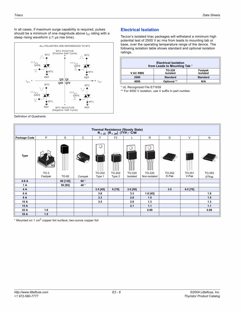
In all cases, if maximum surge capability is required, pulses should be a minimum of one magnitude above IGT rating with a steep rising waveform (≤1 µs rise time).
Definition of Quadrants
Electrical IsolationTeccor’s isolated triac packages will withstand a minimum high potential test of 2500 V ac rms from leads to mounting tab or base, over the operating temperature range of the device. The following isolation table shows standard and optional isolation ratings.
* UL Recognized File E71639** For 4000 V isolation, use V suffix in part number.
* Mounted on 1 cm2 copper foil surface; two-ounce copper foil
MT2 POSITIVE(Positive Half Cycle)
MT2 NEGATIVE(Negative Half Cycle)
MT1
MT2
+ I G T
REFQII
MT1
I G TGATE
MT2
REF
MT1
MT2
REF
MT1
MT2
REF
QIQIV QIII
ALL POLARITIES ARE REFERENCED TO MT1
(-)
I G TGATE
(+)
I G T -
I G TGATE
(-)
I G TGATE
(+)
+
-
Electrical Isolationfrom Leads to Mounting Tab *
V AC RMSTO-220Isolated
FastpakIsolated
2500 Standard Standard4000 Optional ** N/A
Thermal Resistance (Steady State)R θ JC [R θ JA] (TYP.) °C/W
Package Code P E C F F2 L R D V N
Type
TO-3Fastpak TO-92 Compak
TO-202Type 1
TO-202Type 2
TO-220Isolated
TO-220Non-isolated
TO-252D-Pak
TO-251V-Pak
TO-263D2Pak
0.8 A 60 [135] 60 *1 A 50 [95] 40 *4 A 3.5 [45] 6 [70] 3.6 [50] 3.5 6.0 [70]6 A 3.8 3.3 1.8 [45] 1.88 A 3.3 2.8 1.5 1.510 A 3.5 2.6 1.3 1.315 A 2.1 1.1 1.125 A 1.6 0.89 0.8935 A 1.5
Data Sheets Triacs
©2004 Littelfuse, Inc. E2 - 7 http://www.littelfuse.comThyristor Product Catalog +1 972-580-7777
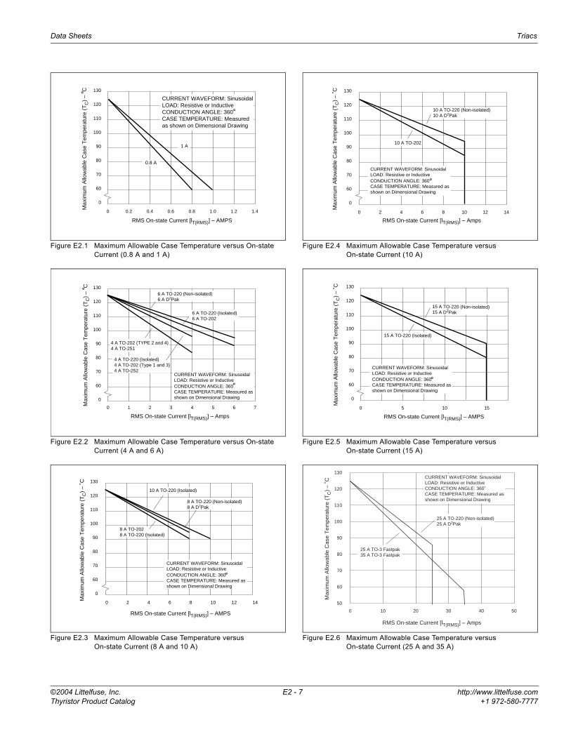
Figure E2.1 Maximum Allowable Case Temperature versus On-state Current (0.8 A and 1 A)
Figure E2.2 Maximum Allowable Case Temperature versus On-state Current (4 A and 6 A)
Figure E2.3 Maximum Allowable Case Temperature versusOn-state Current (8 A and 10 A)
Figure E2.4 Maximum Allowable Case Temperature versusOn-state Current (10 A)
Figure E2.5 Maximum Allowable Case Temperature versusOn-state Current (15 A)
Figure E2.6 Maximum Allowable Case Temperature versusOn-state Current (25 A and 35 A)
0 0.2 0.4 0.6 0.8 1.0 1.2 1.4
0
60
70
80
90
100
110
120
130
RMS On-state Current [lT(RMS)] – AMPS
Max
imum
Allo
wab
le C
ase
Tem
pera
ture
(T
C)
– C
CURRENT WAVEFORM: SinusoidalLOAD: Resistive or InductiveCONDUCTION ANGLE: 360˚CASE TEMPERATURE: Measured as shown on Dimensional Drawing
1 A
0.8 A
0 1 2 3 4 5 6 7
0
60
70
80
90
100
110
120
130
RMS On-state Current [lT(RMS)] – Amps
Max
imum
Allo
wab
le C
ase
Tem
pera
ture
(T
C)
– C
6 A TO-220 (Isolated)6 A TO-202
6 A TO-220 (Non-isolated)6 A D2Pak
4 A TO-220 (Isolated)4 A TO-202 (Type 1 and 3)4 A TO-252
CURRENT WAVEFORM: SinusoidalLOAD: Resistive or InductiveCONDUCTION ANGLE: 360CASE TEMPERATURE: Measured asshown on Dimensional Drawing
4 A TO-202 (TYPE 2 and 4)4 A TO-251
0 2 4 6 8 10 12 14
0
60
70
80
90
100
110
120
130
RMS On-state Current [lT(RMS)] – AMPS
Max
imum
Allo
wab
le C
ase
Tem
pera
ture
(T
C)
– ˚C
10 A TO-220 (Isolated)
8 A TO-220 (Non-isolated)8 A D2Pak
8 A TO-2028 A TO-220 (Isolated)
CURRENT WAVEFORM: SinusoidalLOAD: Resistive or InductiveCONDUCTION ANGLE: 360˚CASE TEMPERATURE: Measured asshown on Dimensional Drawing
0 2 4 6 8 10 12 14
0
60
70
80
90
100
110
120
130
RMS On-state Current [lT(RMS)] – Amps
Max
imum
Allo
wab
le C
ase
Tem
pera
ture
(T
C)
– ˚C
CURRENT WAVEFORM: SinusoidalLOAD: Resistive or InductiveCONDUCTION ANGLE: 360˚CASE TEMPERATURE: Measured asshown on Dimensional Drawing
10 A TO-202
10 A TO-220 (Non-isolated)10 A D2Pak
0 5 10 15
0
60
70
80
90
100
110
120
130
RMS On-state Current [lT(RMS)] – AMPS
Max
imum
Allo
wab
le C
ase
Tem
pera
ture
(T
C)
– ˚C
CURRENT WAVEFORM: SinusoidalLOAD: Resistive or InductiveCONDUCTION ANGLE: 360˚CASE TEMPERATURE: Measured asshown on Dimensional Drawing
15 A TO-220 (Non-isolated)15 A D2Pak
15 A TO-220 (Isolated)
0 10 20 30 40 50
50
60
70
80
90
100
110
120
130
RMS On-state Current [lT(RMS)] – Amps
Max
imum
Allo
wab
le C
ase
Tem
pera
ture
(T
C)
– ˚C
CURRENT WAVEFORM: SinusoidalLOAD: Resistive or InductiveCONDUCTION ANGLE: 360˚CASE TEMPERATURE: Measured asshown on Dimensional Drawing
25 A TO-220 (Non-isolated)25 A D2Pak
25 A TO-3 Fastpak35 A TO-3 Fastpak

Triacs Data Sheets
http://www.littelfuse.com E2 - 8 ©2004 Littelfuse, Inc.+1 972-580-7777 Thyristor Product Catalog
Figure E2.7 Maximum Allowable Ambient Temperature versusOn-state Current
Figure E2.8 On-state Current versus On-state Voltage (Typical)(0.8 A and 1 A)
Figure E2.9 On-state Current versus On-state Voltage (Typical)(4 A, 6 A, 8 A, and 10 A)
Figure E2.10 On-state Current versus On-state Voltage (Typical)(15 A and 25 A)
Figure E2.11 Normalized DC Gate Trigger Current for All Quadrants versus Case Temperature
Figure E2.12 Normalized DC Gate Trigger Voltage for All Quadrants versus Case Temperature
120
100
80
60
40
25
20
0 0.2 0.4 0.6 0.8 1.0 1.2 1.4 1.6 1.8 2.0
TO-220 Devices andTO-202 (Type 1 and 3)
RMS On-state Current [IT (RMS)] — Amps
Max
imum
Allo
wab
le A
mbi
ent T
empe
ratu
re (
TA)
— ˚
C
1 A TO-92
0.8 A TO-92
CURRENT WAVEFORM: SinusoidalLOAD: Resistive or InductiveCONDUCTION ANGLE: 360˚ FREE AIR RATING – NO HEATSINK
TO-202 (TYPE 2 and 4)TO-251
0 0.6 0.8 1.0 1.2 1.4 1.6 1.8
0
1
2
3
4
5
6
7
8
9
10
Positive or Negative Instantaneous On-state Voltage (vT) – Volts
Pos
itive
or N
egat
ive
Inst
anta
neou
s O
n-st
ate
Cur
rent
(iT) –
Am
ps
TC = 25 ˚C
1 A
0.8 A
0 0.6 0.8 1.0 1.2 1.4 1.6 1.8
0
2
4
6
8
10
12
14
16
18
20
Positive or Negative Instantaneous On-state Voltage (vT) – Volts
Pos
itive
or
Neg
ativ
e In
stan
tane
ous
On-
stat
e C
urre
nt (
i T)
– A
mps
TC = 25 ˚C
6-10 A
4A
0 0.6 0.8 1.0 1.2 1.4 1.6 1.8
0
10
20
30
40
50
60
70
80
90
Positive or Negative Instantaneous On-state Voltage (vT) – Volts
Pos
itive
or
Neg
ativ
e In
stan
tane
ous
On-
stat
e C
urre
nt (
i T)
– A
mps
TC = 25 ˚C
15 A and 25 A
25 A and 35 A Fastpak
-65 -40 -15 +25 +65 +125
1.0
2.0
3.0
4.0
Case Temperature (TC) – ˚C
Rat
io o
fI G
T
I GT(T
C =
25
˚C)
-65 -15-40 +25 +65 +125
0
.5
1.0
1.5
2.0
Case Temperature (TC) – ˚C
Rat
io o
fV
GT
VG
T(T
C =
25
˚C)

Data Sheets Triacs
©2004 Littelfuse, Inc. E2 - 9 http://www.littelfuse.comThyristor Product Catalog +1 972-580-7777
Figure E2.13 Peak Surge Current versus Surge Current Duration
Figure E2.14 Normalized DC Holding Current versus Case Temperature Figure E2.15 Turn-on Time versus Gate Trigger Current (Typical)
SUPPLY FREQUENCY: 60 Hz SinusoidalLOAD: ResistiveRMS ON-STATE CURRENT [lT(RMS)]: MaximumRated Value at Specified Case Temperature
NOTES: 1) Gate control may be lost during andimmediately following surge current interval.2) Overload may not be repeated untiljunction temperature has returned tosteady-state rated value.
25 A TO-22015 A10 A8 A
4 A
1 A
6 A
1
10
20
30
405060
80100120
300
400
1000
1 10 100 1000
Surge Current Duration – Full Cycles
Pea
k S
urge
(N
on-r
epet
itive
) O
n-st
ate
Cur
rent
(l T
SM
) –
Am
ps
200
0.8 A
25 A Fastpak
35 A Fastpak
-65 -40 -15 +25 +65 +125
1.0
2.0
3.0
4.0
Case Temperature (TC) – ˚C
Rat
io o
fI H
I H(T
C =
25
˚C)
INITIAL ON-STATE CURRENT= 200 mA DC 0.8 A - 10 A Devices= 400 mA DC 15 A - 25 A Devices
00 25 50 75 100 125 150 175 200 225 250 275 300
1
2
3
4
5
6
7
8
Typ
ical
Tur
n-on
Tim
e (t
gt)
– µS
ec
DC Gate Trigger Current (lGT) – mA
Devices with lGT = 10 mA
Devices with lGT = 25 mA
Devices with lGT = 50 mA
TC = 25 ˚C

Triacs Data Sheets
http://www.littelfuse.com E2 - 10 ©2004 Littelfuse, Inc.+1 972-580-7777 Thyristor Product Catalog
Figure E2.16 Power Dissipation (Typical) versus On-state Current(0.8 A and 1 A)
Figure E2.17 Power Dissipation (Typical) versus On-state Current(6 A to 10 A and 15 A)
Figure E2.18 Power Dissipation (Typical) versus On-state Current(25 A to 35 A)
Figure E2.19 Power Dissipation (Typical) versus RMS On-state Current(4 A)
RMS On-state Current [IT(RMS)] – Amps
Ave
rage
On-
stat
e P
ower
Dis
sipa
tion
[PD
(AV
)] –
Wat
ts
0 0.25 0.50 0.75 1.0 1.25
0
0.5
1.0
1.5CURRENT WAVEFORM: SinusoidalLOAD: Resistive or InductiveCONDUCTION ANGLE: 360˚
1 A
0.8 A
0 1 2 3 4 5 6 7 8 9 10 11 12 13 14 15 16
0
2
4
6
8
10
12
14
16
18
RMS On-state Current [lT(RMS)] – Amps
Ave
rage
On-
stat
e P
ower
Dis
sipa
tion
[PD
(AV
)] –
Wat
ts
6-10 A
15 A
CURRENT WAVEFORM: SinusoidalLOAD: Resistive or InductiveCONDUCTION ANGLE: 360˚
0 8 16 24 32 40
0
5
10
15
20
25
30
35
40
45
RMS On-state Current [lT(RMS)] – Amps
Ave
rage
On-
stat
e P
ower
Dis
sipa
tion
[PD
(AV
)] –
Wat
ts
CURRENT WAVEFORM: SinusoidalLOAD: Resistive or InductiveCONDUCTION ANGLE: 360˚
25 A
25 A - 35 A Fastpaks
RMS On-state Current [IT(RMS)] – Amps
Ave
rage
On-
stat
e P
ower
Dis
sipa
tion
[PD
(AV
)] –
Wat
ts
0 1.0 2.0 3.0 4.0
0
1.0
2.0
3.0
CURRENT WAVEFORM: SinusoidalLOAD: Resistive or InductiveCONDUCTION ANGLE: 360˚
4 A
4.0
©2004 Littelfuse, Inc. E3 - 1 http://www.littelfuse.comThyristor Product Catalog +1 972-580-7777
U.L
. REC
OG
NIZ
ED
File #E71639
QuadracInternally Triggered Triacs (4 A to 15 A)
E3General DescriptionTeccor’s Quadrac devices are triacs that include a diac trigger mounted inside the same package. This device, developed by Teccor, saves the user the expense and assembly time of buying a discrete diac and assembling in conjunction with a gated triac. Also, the alternistor Quadrac device (QxxxxLTH) eliminates the need for a snubber network.The Quadrac device is a bidirectional AC switch and is gate con-trolled for either polarity of main terminal voltage. Its primary pur-pose is for AC switching and phase control applications such as speed controls, temperature modulation controls, and lighting controls where noise immunity is required. Triac current capacities range from 4 A to 15 A with voltage ranges from 200 V to 600 V. Quadrac devices are available in the TO-220 package.The TO-220 package is electrically isolated to 2500 V rms from the leads to mounting surface. 4000 V rms is available on special order. This means that no external isolation is required, thus eliminating the need for separate insulators and insulator-mount-ing steps and saving dollars over “hot tab” devices.
All Teccor triac and diac chips have glass-passivated junctions to ensure long-term device reliability and parameter stability.Variations of devices in this data sheet are available for custom design applications. Consult the factory for more information.
Features• Glass-passivated junctions• Electrically-isolated package• Internal trigger diac• High surge capability — up to 200 A• High voltage capability — 200 V to 600 V
TO-220
MT2 MT1
T
E3

Quadrac Data Sheets
http://www.littelfuse.com E3 - 2 ©2004 Littelfuse, Inc.+1 972-580-7777 Thyristor Product Catalog
Specific Test Conditions[∆V±] — Dynamic breakback voltage (forward and reverse)∆VBO — Breakover voltage symmetryCT — Trigger firing capacitancedi/dt — Maximum rate-of-change of on-state currentdv/dt — Critical rate-of-rise of off-state voltage at rated VDRM gate opendv/dt(c) — Critical rate-of-rise of commutation voltage at rated VDRM
and IT(RMS) commutating di/dt = 0.54 rated IT(RMS)/ms; gate unenergized
I2t — RMS surge (non-repetitive) on-state current for period of 8.3 ms for fusing
IBO — Peak breakover currentIDRM — Peak off-state current gate open; VDRM = maximum rated valueIGTM — Peak gate trigger current (10 µs Max)IH — Holding current; gate openIT(RMS) — RMS on-state current, conduction angle of 360°ITSM — Peak one-cycle surgetgt — Gate controlled turn-on timeVBO — Breakover voltage (forward and reverse)
VDRM — Repetitive peak blocking voltageVTM — Peak on-state voltage at maximum rated RMS current
General Notes• All measurements are made at 60 Hz with resistive load at an ambi-
ent temperature of +25 °C unless otherwise specified.• Operating temperature range (TJ) is -40 °C to +125 °C.• Storage temperature range (TS) is -40 °C to +125 °C.• Lead solder temperature is a maximum of +230 °C for 10 seconds
maximum; ≥1/16" (1.59 mm) from case.• The case temperature (TC) is measured as shown on dimensional
outline drawings. See “Package Dimensions” section of this catalog.
Electrical Specification Notes(1) For either polarity of MT2 with reference to MT1(2) See Figure E3.1 for IH versus TC.(3) See Figure E3.4 and Figure E3.5 for iT versus vT.(4) See Figure E3.9 for surge ratings with specific durations.
IT(RMS)
Part No.VDRM IDRM VTM
Trigger Diac Specifications (T–MT1)Isolated ∆VBO VBO [∆V± ] IBO CT
(5)
TO-220
(1)
Volts
(1) (10)
mAmps
(1) (3)
Volts
(7)
Volts
(6)
Volts
(6)
Volts µAmps
(11)
µFaradsTC = 25 °C
TC = 100 °C
TC = 125 °C TC = 25 °C
See “Package Dimensions” section for variations. (12) MIN MAX MAX MAX MIN MAX MIN MAX MAX
4 AQ2004LT 200 0.05 0.5 2 1.6 3 33 43 5 25 0.1Q4004LT 400 0.05 0.5 2 1.6 3 33 43 5 25 0.1Q6004LT 600 0.05 0.5 2 1.6 3 33 43 5 25 0.1
6 A
Q2006LT 200 0.05 0.5 2 1.6 3 33 43 5 25 0.1Q4006LT 400 0.05 0.5 2 1.6 3 33 43 5 25 0.1Q6006LT 600 0.05 0.5 2 1.6 3 33 43 5 25 0.1
Q4006LTH 400 0.05 0.5 2 1.6 3 33 43 5 25 0.1Q6006LTH 600 0.05 0.5 2 1.6 3 33 43 5 25 0.1
8 A
Q2008LT 200 0.05 0.5 2 1.6 3 33 43 5 25 0.1Q4008LT 400 0.05 0.5 2 1.6 3 33 43 5 25 0.1Q6008LT 600 0.05 0.5 2 1.6 3 33 43 5 25 0.1
Q4008LTH 400 0.05 0.5 2 1.6 3 33 43 5 25 0.1Q6008LTH 600 0.05 0.5 2 1.6 3 33 43 5 25 0.1
10 A
Q2010LT 200 0.05 0.5 2 1.6 3 33 43 5 25 0.1Q4010LT 400 0.05 0.5 2 1.6 3 33 43 5 25 0.1Q6010LT 600 0.05 0.5 2 1.6 3 33 43 5 25 0.1
Q4010LTH 400 0.05 0.5 2 1.6 3 33 43 5 25 0.1Q6010LTH 600 0.05 0.5 2 1.6 3 33 43 5 25 0.1
15 A
Q2015LT 200 0.05 0.5 2 1.6 3 33 43 5 25 0.1Q4015LT 400 0.05 0.5 2 1.6 3 33 43 5 25 0.1Q6015LT 600 0.05 0.5 2 1.6 3 33 43 5 25 0.1
Q4015LTH 400 0.05 0.5 2 1.6 3 33 43 5 25 0.1Q6015LTH 600 0.05 0.5 2 1.6 3 33 43 5 25 0.1
MT1
MT2
T

Data Sheets Quadrac
©2004 Littelfuse, Inc. E3 - 3 http://www.littelfuse.comThyristor Product Catalog +1 972-580-7777
(5) See Figure E3.6, Figure E3.7, and Figure E3.8 for current rating at specific operating temperature.
(6) See Figure E3.2 and Figure E3.3 for test circuit.(7) ∆VBO = [+ VBO] - [- VBO](8) See Figure E3.7 and Figure E3.8 for maximum allowable case
temperature at maximum rated current.(9) Trigger firing capacitance = 0.1 µF with 0.1 µs rise time(10) TC = TJ for test conditions in off state(11) Maximum required value to ensure sufficient gate current(12) See package outlines for lead form configurations. When ordering
special lead forming, add type number as suffix to part number.
Electrical IsolationAll Teccor isolated Quadrac packages withstand a minimum high potential test of 2500 V ac rms from leads to mounting tab over the operating temperature range of the device. The following iso-lation table shows standard and optional isolation ratings.
* UL Recognized File #E71639**For 4000 V isolation, use “V” suffix in part number.
IH ITSM dv/dt(c) dv/dt tgt I2t IGTM di/dt(1) (2)
mAmps
(4) (8)
Amps
(1) (5) (8)
Volts/µSec
(1)
Volts/µSec
(6) (9)
µSec Amps2Sec Amps
(9)
Amps/µSecTC =
100 °CTC =
125 °C
MAX 60/50Hz MIN MIN TYP40 55/46 3 75 50 3 12.5 1.2 5040 55/46 3 75 50 3 12.5 1.2 5040 55/46 3 50 50 3 12.5 1.2 5050 80/65 4 150 100 3 26.5 1.5 7050 80/65 4 150 100 3 26.5 1.5 7050 80/65 4 125 85 3 26.5 1.5 7050 80/65 25 575 450 3 26.5 1.5 7050 80/65 25 425 350 3 26.5 1.5 7060 100/83 4 175 120 3 41 1.5 7060 100/83 4 175 120 3 41 1.5 7060 100/83 4 150 100 3 41 1.5 7060 100/83 25 575 450 3 41 1.5 7060 100/83 25 425 350 3 41 1.5 7060 120/100 4 200 150 3 60 1.5 7060 120/100 4 200 150 3 60 1.5 7060 120/100 4 175 120 3 60 1.5 7060 120/100 30 925 700 3 60 1.5 7060 120/100 30 775 600 3 60 1.5 7070 200/167 4 300 200 3 166 1.5 10070 200/167 4 300 200 3 166 1.5 10070 200/167 4 200 150 3 166 1.5 10070 200/167 30 925 700 3 166 1.5 10070 200/167 30 775 600 3 166 1.5 100
Thermal Resistance (Steady State)RθJC [RθJA] °C/W (TYP)
TYPE Isolated TO-2204 A 3.6 [50]6 A 3.38 A 2.810 A 2.615 A 2.1
Electrical Isolation from Leads to Mounting Tab *
V AC RMS TYPE2500 Standard4000 Optional **
Quadrac Data Sheets
http://www.littelfuse.com E3 - 4 ©2004 Littelfuse, Inc.+1 972-580-7777 Thyristor Product Catalog
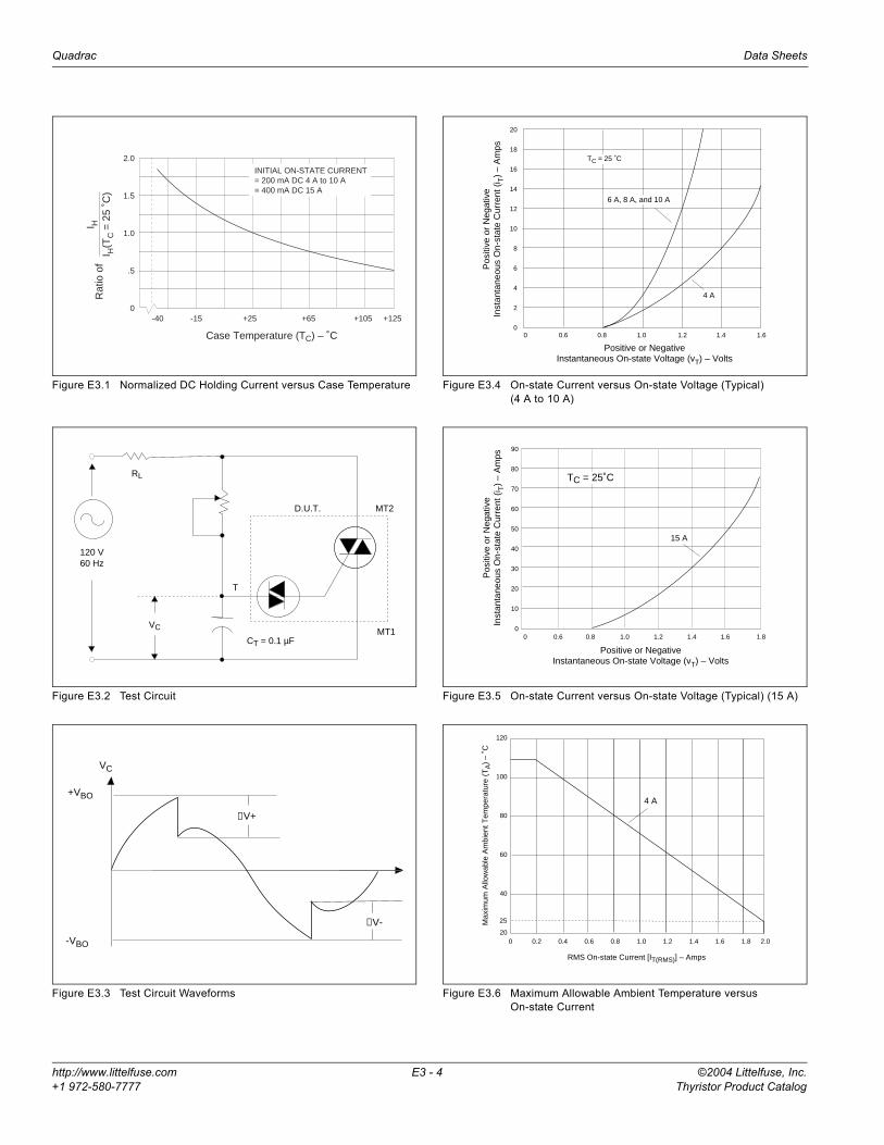
Figure E3.1 Normalized DC Holding Current versus Case Temperature
Figure E3.2 Test Circuit
Figure E3.3 Test Circuit Waveforms
Figure E3.4 On-state Current versus On-state Voltage (Typical)(4 A to 10 A)
Figure E3.5 On-state Current versus On-state Voltage (Typical) (15 A)
Figure E3.6 Maximum Allowable Ambient Temperature versus On-state Current
Case Temperature (TC) – ˚C
-40 -15 +25 +65 +105
I HI H
(TC
= 2
5 ˚C
)
2.0
1.5
1.0
.5
0
INITIAL ON-STATE CURRENT= 200 mA DC 4 A to 10 A= 400 mA DC 15 A
Rat
io o
f
+125
120 V60 Hz
RL
D.U.T. MT2
MT1VC
CT = 0.1 µF
T
VC
∆V+
-VBO
∆V-
+VBO
20
18
16
14
12
10
8
6
4
2
00 0.6 0.8 1.0 1.2 1.4 1.6
Pos
itive
or
Neg
ativ
eIn
stan
tane
ous
On-
stat
e C
urre
nt (
i T)
– A
mps
Positive or NegativeInstantaneous On-state Voltage (vT) – Volts
6 A, 8 A, and 10 A
4 A
TC = 25 ˚C
90
80
70
60
50
40
30
20
10
00 0.6 0.8 1.0 1.2 1.4 1.6
Pos
itive
or
Neg
ativ
eIn
stan
tane
ous
On-
stat
e C
urre
nt (
i T)
– A
mps
15 A
TC = 25˚C
1.8
Positive or NegativeInstantaneous On-state Voltage (vT) – Volts
120
100
80
60
40
20
RMS On-state Current [IT(RMS)] – Amps
Max
imum
Allo
wab
le A
mbi
ent T
empe
ratu
re (
TA
) –
˚C
25
0 0.2 0.4 0.6 0.8 1.0 1.2 1.4 1.6 1.8 2.0
4 A

Data Sheets Quadrac
©2004 Littelfuse, Inc. E3 - 5 http://www.littelfuse.comThyristor Product Catalog +1 972-580-7777
Figure E3.7 Maximum Allowable Case Temperature versus On-state Current (4 A)
Figure E3.8 Maximum Allowable Case Temperature versus On-state Current (6 A to 15 A)
Figure E3.9 Peak Surge Current versus Surge Current Duration
Figure E3.10 Power Dissipation (Typical) versus On-state Current (4 A)
Figure E3.11 Power Dissipation (Typical) versus On-state Current(6 A to 10 A and 15 A)
Figure E3.12 Normalized diac VBO versus Junction Temperature
RMS On-state Current [IT(RMS)] – Amps
0 .5 1.0 1.5 2.0 2.5 3.0 3.5 4.0 4.5 5.0
Max
imum
Allo
wab
le C
ase
Tem
pera
ture
(T
C)
– ˚C CURRENT WAVEFORM: Sinusoidal
LOAD: Resistive or InductiveCONDUCTION ANGLE: 360CASE TEMPERATURE: Measuredas shown on Dimensional Drawings
130
120
110
100
90
80
70
600
4 A
RMS On-state Current [IT(RMS)] – Amps
0 2.0 4.0 6.0 8.0 10.0 12.0 14.0 16.0 18.0 20.0
Max
imum
Allo
wab
le C
ase
Tem
pera
ture
(T
C)
– ˚C CURRENT WAVEFORM: Sinusoidal
LOAD: Resistive or InductiveCONDUCTION ANGLE: 360CASE TEMPERATURE: Measuredas shown on Dimensional Drawings
130
120
110
100
90
80
70
60
0
6 A
10 A8 A
15 A
200
120
40
1 2 3 4 5 6 8 10 20 3040 60 80 100 200 300 600 1000
80
6050
100
8
65
10
30
20
4
1
3
2
Surge Current Duration – Full Cycles
Pea
k S
urge
(N
on-r
epet
itive
)O
n-st
ate
Cur
rent
(I T
SM
) –
Am
ps
SUPPLY FREQUENCY: 60 Hz SinusoidalLOAD: ResistiveRMS ON-STATE CURRENT [IT(RMS)]: Maximum Rated Value at Specified Case Temperature
NOTES:1) Gates control may be lost duringand immediately following surgecurrent interval.2) Overload may not be repeated untiljunction temperature has returned tosteady state rated value.
15 A
10 A8 A
6 A
4 A
Ave
rage
On-
stat
e P
ower
Dis
sipa
tion
[PD
(AV
)] – W
atts
RMS On-state Current [IT(RMS)] – Amps
4.0
3.0
2.0
1.0
00 1.0 2.0 3.0 4.0 5.0
CURRENT WAVEFORM: SinusoidalLOAD: Resistive or InductiveCONDUCTION ANGLE: 360˚
4 A
CURRENT WAVEFORM: SinusoidalLOAD: Resistive or InductiveCONDUCTION ANGLE: 360˚
18
16
14
12
10
8
6
4
2
01614121086420
RMS On-state Current [IT(RMS)] – Amps
Ave
rage
On-
stat
e P
ower
Dis
sipa
tion
[PD
(AV
)] – W
atts
15 A
6 A to 10 A
-8
-6
-4
-2
0
+2
+4
-40 -20 0 +20 +40 +60 +80 +100 +120 +140
Junction Temperature (TJ) – ˚C
Per
cent
age
of V
BO C
hang
e –
%

Notes
©2004 Littelfuse, Inc. E4 - 1 http://www.littelfuse.comThyristor Product Catalog +1 972-580-7777
* Selecte
d Pack
ages
U.L
. RECO
GNIZ
ED
File #E
7163
9
Alternistor Triacs(6 A to 40 A)
E4General DescriptionTeccor offers bidirectional alternistors with current ratings from 6 A to 40 A and voltages from 200 V to 1000 V as part of Tec-cor's broad line of thyristors. Teccor's alternistor is specifically designed for applications that switch highly inductive loads. A special chip offers the same performance as two thyristors (SCRs) wired inverse parallel (back-to-back), providing better turn-off behavior than a standard triac. An alternistor may be trig-gered from a blocking to conduction state for either polarity of applied AC voltage with operating modes in Quadrants I, II, and III.This new chip construction provides two electrically separate SCR structures, providing enhanced dv/dt characteristics while retaining the advantages of a single-chip device.All alternistors have glass-passivated junctions to ensure long-term reliability and parameter stability. Teccor's glass-passivated junctions offer a reliable barrier against junction contamination.Teccor's TO-218X package is designed for heavy, steady power-handling capability. It features large eyelet terminals for ease of soldering heavy gauge hook-up wire. All the isolated packages have a standard isolation voltage rating of 2500 V rms.
Variations of devices covered in this data sheet are available for custom design applications. Consult the factory for further information.
Features• High surge current capability• Glass-passivated junctions• 2500 V ac isolation for L, J, and K Packages• High commutating dv/dt• High static dv/dt
*TO-220
*TO-218
*TO-218X
MT2 MT1
G
E4
TO-263D2Pak
TO-252D-Pak
TO-251V-Pak
Alternistor Triacs Data Sheets
http://www.littelfuse.com E4 - 2 ©2004 Littelfuse, Inc.+1 972-580-7777 Thyristor Product Catalog
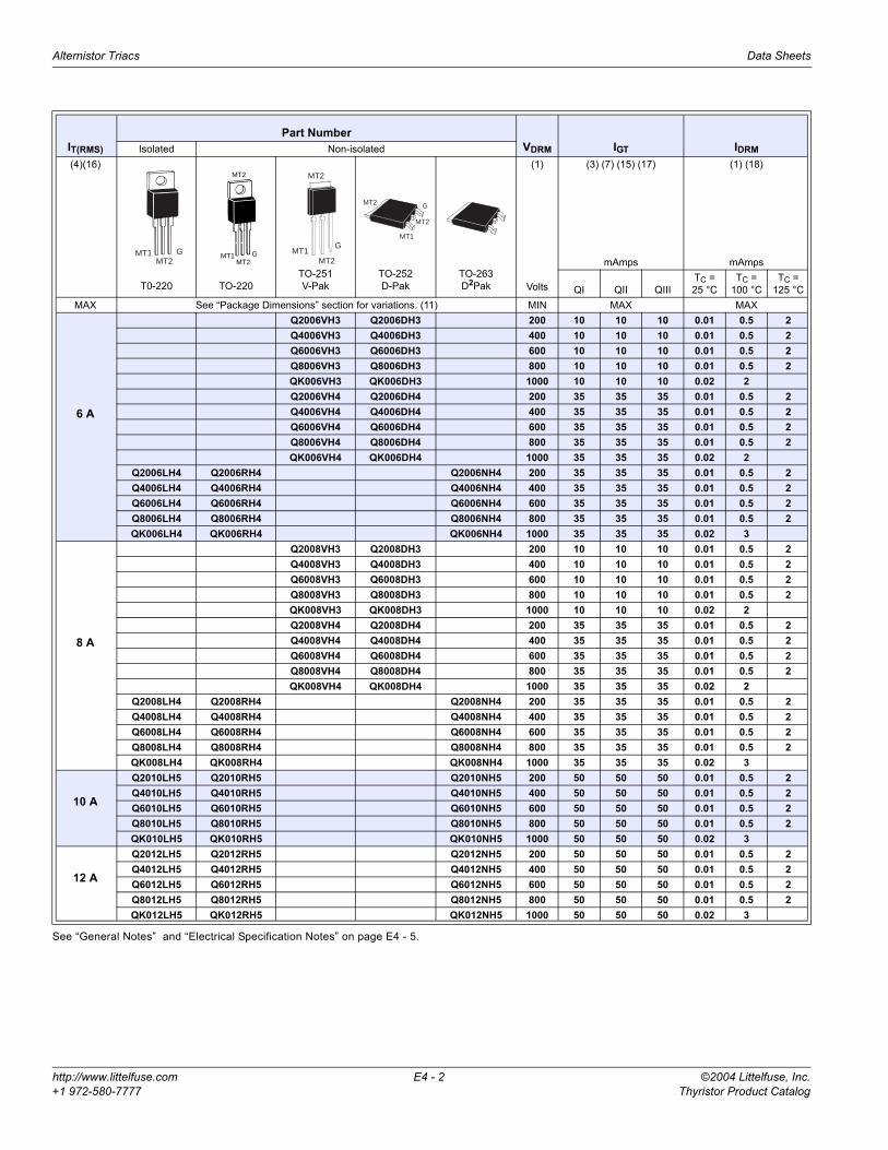
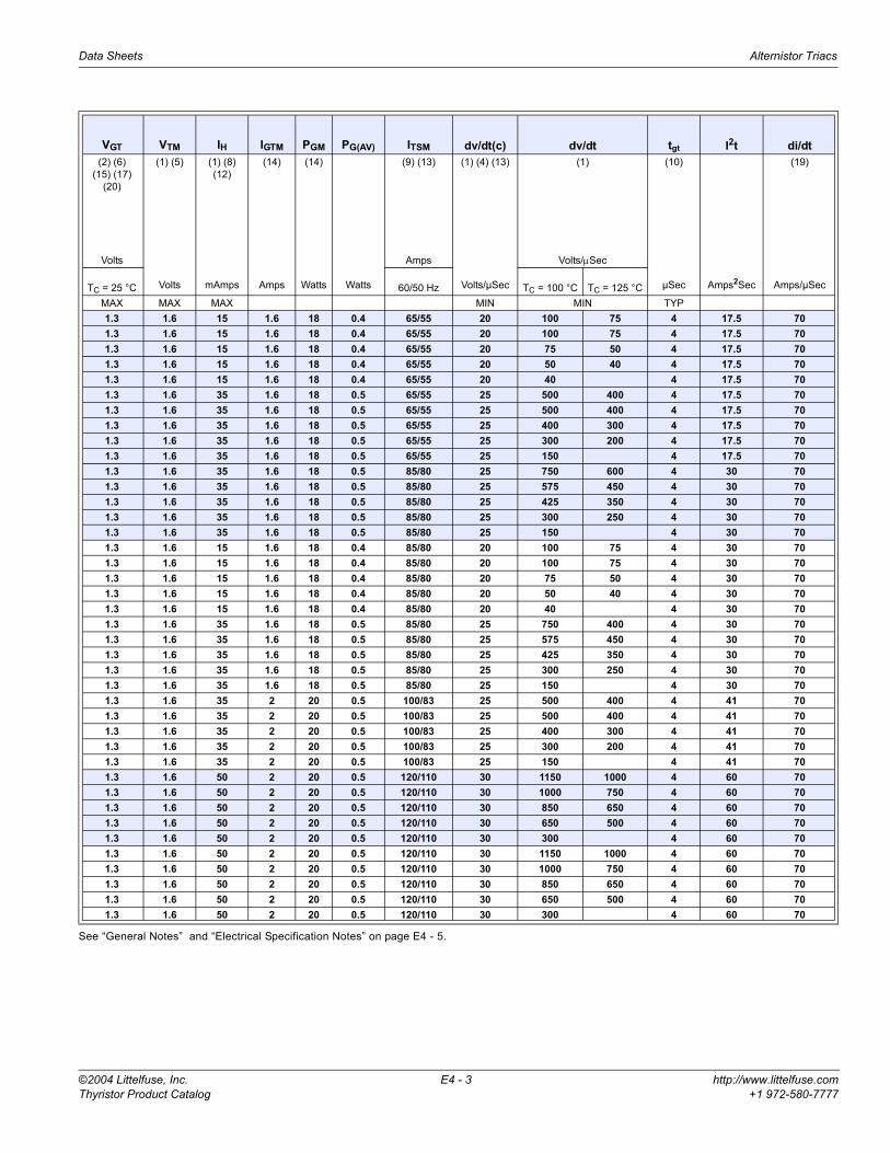
See “General Notes” and “Electrical Specification Notes” on page E4 - 5.
IT(RMS)
Part NumberVDRM IGT IDRMIsolated Non-isolated
(4)(16)
T0-220 TO-220TO-251V-Pak
TO-252D-Pak
TO-263D2Pak
(1)
Volts
(3) (7) (15) (17)
mAmps
(1) (18)
mAmps
QI QII QIIITC =25 °C
TC =100 °C
TC =125 °C
MAX See “Package Dimensions” section for variations. (11) MIN MAX MAX
6 A
Q2006VH3 Q2006DH3 200 10 10 10 0.01 0.5 2Q4006VH3 Q4006DH3 400 10 10 10 0.01 0.5 2Q6006VH3 Q6006DH3 600 10 10 10 0.01 0.5 2Q8006VH3 Q8006DH3 800 10 10 10 0.01 0.5 2QK006VH3 QK006DH3 1000 10 10 10 0.02 2Q2006VH4 Q2006DH4 200 35 35 35 0.01 0.5 2Q4006VH4 Q4006DH4 400 35 35 35 0.01 0.5 2Q6006VH4 Q6006DH4 600 35 35 35 0.01 0.5 2Q8006VH4 Q8006DH4 800 35 35 35 0.01 0.5 2QK006VH4 QK006DH4 1000 35 35 35 0.02 2
Q2006LH4 Q2006RH4 Q2006NH4 200 35 35 35 0.01 0.5 2Q4006LH4 Q4006RH4 Q4006NH4 400 35 35 35 0.01 0.5 2Q6006LH4 Q6006RH4 Q6006NH4 600 35 35 35 0.01 0.5 2Q8006LH4 Q8006RH4 Q8006NH4 800 35 35 35 0.01 0.5 2QK006LH4 QK006RH4 QK006NH4 1000 35 35 35 0.02 3
8 A
Q2008VH3 Q2008DH3 200 10 10 10 0.01 0.5 2Q4008VH3 Q4008DH3 400 10 10 10 0.01 0.5 2Q6008VH3 Q6008DH3 600 10 10 10 0.01 0.5 2Q8008VH3 Q8008DH3 800 10 10 10 0.01 0.5 2QK008VH3 QK008DH3 1000 10 10 10 0.02 2Q2008VH4 Q2008DH4 200 35 35 35 0.01 0.5 2Q4008VH4 Q4008DH4 400 35 35 35 0.01 0.5 2Q6008VH4 Q6008DH4 600 35 35 35 0.01 0.5 2Q8008VH4 Q8008DH4 800 35 35 35 0.01 0.5 2QK008VH4 QK008DH4 1000 35 35 35 0.02 2
Q2008LH4 Q2008RH4 Q2008NH4 200 35 35 35 0.01 0.5 2Q4008LH4 Q4008RH4 Q4008NH4 400 35 35 35 0.01 0.5 2Q6008LH4 Q6008RH4 Q6008NH4 600 35 35 35 0.01 0.5 2Q8008LH4 Q8008RH4 Q8008NH4 800 35 35 35 0.01 0.5 2QK008LH4 QK008RH4 QK008NH4 1000 35 35 35 0.02 3
10 A
Q2010LH5 Q2010RH5 Q2010NH5 200 50 50 50 0.01 0.5 2Q4010LH5 Q4010RH5 Q4010NH5 400 50 50 50 0.01 0.5 2Q6010LH5 Q6010RH5 Q6010NH5 600 50 50 50 0.01 0.5 2Q8010LH5 Q8010RH5 Q8010NH5 800 50 50 50 0.01 0.5 2QK010LH5 QK010RH5 QK010NH5 1000 50 50 50 0.02 3
12 A
Q2012LH5 Q2012RH5 Q2012NH5 200 50 50 50 0.01 0.5 2Q4012LH5 Q4012RH5 Q4012NH5 400 50 50 50 0.01 0.5 2Q6012LH5 Q6012RH5 Q6012NH5 600 50 50 50 0.01 0.5 2Q8012LH5 Q8012RH5 Q8012NH5 800 50 50 50 0.01 0.5 2QK012LH5 QK012RH5 QK012NH5 1000 50 50 50 0.02 3
MT1MT2
G MT1 GMT2
MT2 MT2
MT2
GMT1
MT2
MT2
MT1
G
Data Sheets Alternistor Triacs
©2004 Littelfuse, Inc. E4 - 3 http://www.littelfuse.comThyristor Product Catalog +1 972-580-7777
See “General Notes” and “Electrical Specification Notes” on page E4 - 5.
VGT VTM IH IGTM PGM PG(AV) ITSM dv/dt(c) dv/dt tgt I2t di/dt(2) (6)
(15) (17)(20)
Volts
(1) (5)
Volts
(1) (8)(12)
mAmps
(14)
Amps
(14)
Watts Watts
(9) (13)
Amps
(1) (4) (13)
Volts/µSec
(1)
Volts/µSec
(10)
µSec Amps2Sec
(19)
Amps/µSecTC = 25 °C 60/50 Hz TC = 100 °C TC = 125 °CMAX MAX MAX MIN MIN TYP1.3 1.6 15 1.6 18 0.4 65/55 20 100 75 4 17.5 701.3 1.6 15 1.6 18 0.4 65/55 20 100 75 4 17.5 701.3 1.6 15 1.6 18 0.4 65/55 20 75 50 4 17.5 701.3 1.6 15 1.6 18 0.4 65/55 20 50 40 4 17.5 701.3 1.6 15 1.6 18 0.4 65/55 20 40 4 17.5 701.3 1.6 35 1.6 18 0.5 65/55 25 500 400 4 17.5 701.3 1.6 35 1.6 18 0.5 65/55 25 500 400 4 17.5 701.3 1.6 35 1.6 18 0.5 65/55 25 400 300 4 17.5 701.3 1.6 35 1.6 18 0.5 65/55 25 300 200 4 17.5 701.3 1.6 35 1.6 18 0.5 65/55 25 150 4 17.5 701.3 1.6 35 1.6 18 0.5 85/80 25 750 600 4 30 701.3 1.6 35 1.6 18 0.5 85/80 25 575 450 4 30 701.3 1.6 35 1.6 18 0.5 85/80 25 425 350 4 30 701.3 1.6 35 1.6 18 0.5 85/80 25 300 250 4 30 701.3 1.6 35 1.6 18 0.5 85/80 25 150 4 30 701.3 1.6 15 1.6 18 0.4 85/80 20 100 75 4 30 701.3 1.6 15 1.6 18 0.4 85/80 20 100 75 4 30 701.3 1.6 15 1.6 18 0.4 85/80 20 75 50 4 30 701.3 1.6 15 1.6 18 0.4 85/80 20 50 40 4 30 701.3 1.6 15 1.6 18 0.4 85/80 20 40 4 30 701.3 1.6 35 1.6 18 0.5 85/80 25 750 400 4 30 701.3 1.6 35 1.6 18 0.5 85/80 25 575 450 4 30 701.3 1.6 35 1.6 18 0.5 85/80 25 425 350 4 30 701.3 1.6 35 1.6 18 0.5 85/80 25 300 250 4 30 701.3 1.6 35 1.6 18 0.5 85/80 25 150 4 30 701.3 1.6 35 2 20 0.5 100/83 25 500 400 4 41 701.3 1.6 35 2 20 0.5 100/83 25 500 400 4 41 701.3 1.6 35 2 20 0.5 100/83 25 400 300 4 41 701.3 1.6 35 2 20 0.5 100/83 25 300 200 4 41 701.3 1.6 35 2 20 0.5 100/83 25 150 4 41 701.3 1.6 50 2 20 0.5 120/110 30 1150 1000 4 60 701.3 1.6 50 2 20 0.5 120/110 30 1000 750 4 60 701.3 1.6 50 2 20 0.5 120/110 30 850 650 4 60 701.3 1.6 50 2 20 0.5 120/110 30 650 500 4 60 701.3 1.6 50 2 20 0.5 120/110 30 300 4 60 701.3 1.6 50 2 20 0.5 120/110 30 1150 1000 4 60 701.3 1.6 50 2 20 0.5 120/110 30 1000 750 4 60 701.3 1.6 50 2 20 0.5 120/110 30 850 650 4 60 701.3 1.6 50 2 20 0.5 120/110 30 650 500 4 60 701.3 1.6 50 2 20 0.5 120/110 30 300 4 60 70

Alternistor Triacs Data Sheets
http://www.littelfuse.com E4 - 4 ©2004 Littelfuse, Inc.+1 972-580-7777 Thyristor Product Catalog
See “General Notes” and “Electrical Specification Notes” on page E4 - 5.
Test Conditionsdi/dt — Maximum rate-of-change of on-state currentdv/dt — Critical rate-of-rise of off-state voltage at rated VDRM gate opendv/dt(c) — Critical rate-of-rise of commutation voltage at rated VDRM
and IT(RMS) commutating di/dt = 0.54 rated IT(RMS)/ms; gate unenergized
I2t — RMS surge (non-repetitive) on-state current for period of 8.3 ms for fusing
IDRM — Peak off-state current gate open; VDRM = maximum rated valueIGT — DC gate trigger current in specific operating quadrants;
VD = 12 V dcIGTM — Peak gate trigger current
IH — Holding current (DC); gate openIT(RMS) — RMS on-state current conduction angle of 360°ITSM — Peak one-cycle surgePG(AV) — Average gate power dissipationPGM — Peak gate power dissipation; IGT ≤ IGTM
tgt — Gate controlled turn-on time; IGT = 300 mA with 0.1 µs rise timeVDRM — Repetitive peak blocking voltageVGT — DC gate trigger voltage; VD = 12 V dcVTM — Peak on-state voltage at maximum rated RMS current
IT(RMS)
Part NumberVDRM IGTIsolated Non-isolated
(4)(16)
T0-220TO-218
(16) TO-218X TO-220TO-263D2Pak
(1)
Volts
(3) (7) (15) (17)
mAmps
QI QII QIIIMAX See “Package Dimensions” section for variations. (11) MAX
16 A
Q2016LH3 Q2016RH3 Q2016NH3 200 20 20 20Q4016LH3 Q4016RH3 Q4016NH3 400 20 20 20Q6016LH3 Q6016RH3 Q6016NH3 600 20 20 20Q8016LH3 Q8016RH3 Q8016NH3 800 20 20 20QK016LH3 QK016RH3 QK016NH3 1000 20 20 20Q2016LH4 Q2016RH4 Q2016NH4 200 35 35 35Q4016LH4 Q4016RH4 Q4016NH4 400 35 35 35Q6016LH4 Q6016RH4 Q6016NH4 600 35 35 35Q8016LH4 Q8016RH4 Q8016NH4 800 35 35 35QK016LH4 QK016RH4 QK016NH4 1000 35 35 35Q2016LH6 Q2016RH6 Q2016NH6 200 80 80 80Q4016LH6 Q4016RH6 Q4016NH6 400 80 80 80Q6016LH6 Q6016RH6 Q6016NH6 600 80 80 80Q8016LH6 Q8016RH6 Q8016NH6 800 80 80 80QK016LH6 QK016RH6 QK016NH6 1000 80 80 80
25 A
Q2025L6 Q2025K6 Q2025J6 Q2025R6 Q2025NH6 200 80 80 80Q4025L6 Q4025K6 Q4025J6 Q4025R6 Q4025NH6 400 80 80 80Q6025L6 Q6025K6 Q6025J6 Q6025R6 Q6025NH6 600 80 80 80Q8025L6 Q8025K6 Q8025J6 Q8025R6 Q8025NH6 800 80 80 80QK025L6 QK025K6 QK025R6 QK025NH6 1000 80 80 80
30 AQ2030LH5 200 50 50 50Q4030LH5 400 50 50 50Q6030LH5 600 50 50 50
35 AQ2035RH5 Q2035NH5 200 50 50 50Q4035RH5 Q4035NH5 400 50 50 50Q6035RH5 Q6035NH5 600 50 50 50
40 A
Q2040K7 Q2040J7 200 100 100 100Q4040K7 Q4040J7 400 100 100 100Q6040K7 Q6040J7 600 100 100 100Q8040K7 Q8040J7 800 100 100 100QK040K7 1000 100 100 100
MT1MT2
GMT1
GMT2 MT1
G
MT2MT1 G
MT2
MT2
MT2
MT2
MT1
G

Data Sheets Alternistor Triacs
©2004 Littelfuse, Inc. E4 - 5 http://www.littelfuse.comThyristor Product Catalog +1 972-580-7777
General Notes• All measurements are made at 60 Hz with a resistive load at an
ambient temperature of +25 °C unless specified otherwise.• Operating temperature range (TJ) is -40 °C to +125 °C.• Storage temperature range (TS) is -40 °C to +125 °C.• Lead solder temperature is a maximum of 230 °C for 10 seconds
maximum ≥1/16" (1.59 mm) from case.• The case temperature (TC) is measured as shown in the dimen-
sional outline drawings. See “Package Dimensions” section.
Electrical Specification Notes(1) For either polarity of MT2 with reference to MT1 terminal(2) For either polarity of gate voltage (VGT) with reference to MT1
terminal(3) See Gate Characteristics and Definition of Quadrants.(4) See Figure E4.1 through Figure E4.4 for current rating at specific
operating temperature and Figure 4.16 for free air rating (no heat sink).
(5) See Figure E4.5 and Figure E4.6 for iT and vT.(6) See Figure E4.7 for VGT versus TC.(7) See Figure E4.8 for IGT versus TC.
(8) See Figure E4.9 for IH versus TC.(9) See Figure E4.10 and Figure E4.11 for surge rating with specific
durations.
IDRM VGT VTM IH IGTM PGM PG(AV) ITSM dv/dt(c) dv/dt tgt I2t di/dt(1) (18)
mAmps
(2) (6)(15) (17)
(20)
Volts
(1) (5)
Volts
(1) (8)(12)
mAmps
(14)
Amps
(14)
Watts Watts
(9) (13)
Amps
(1) (4) (13)
Volts/µSec
(1)
Volts/µSec
(10)
µSec Amps2Sec
(19)
Amps/µSecTC =25 °C
TC =100 °C
TC =125 °C
TC =25 °C
TC = 25 °C 60/50 Hz
TC =100 °C
TC =125 °C
MAX MAX MAX MAX MIN MIN TYP0.05 0.5 2 1.5 1.6 35 2 20 0.5 200/167 20 500 400 3 166 1000.05 0.5 2 1.5 1.6 35 2 20 0.5 200/167 20 400 350 3 166 1000.05 0.5 2 1.5 1.6 35 2 20 0.5 200/167 20 300 250 3 166 1000.1 1 3 1.5 1.6 35 2 20 0.5 200/167 20 275 200 3 166 1000.1 3 1.5 1.6 35 2 20 0.5 200/167 20 200 3 166 1000.05 0.5 2 2 1.6 50 2 20 0.5 200/167 25 650 500 3 166 1000.05 0.5 2 2 1.6 50 2 20 0.5 200/167 25 600 475 3 166 1000.05 0.5 2 2 1.6 50 2 20 0.5 200/167 25 500 400 3 166 1000.1 1 3 2 1.6 50 2 20 0.5 200/167 25 425 350 3 166 1000.1 3 2 1.6 50 2 20 0.5 200/167 25 300 3 166 1000.05 0.5 2 2.5 1.6 70 2 20 0.5 200/167 30 875 600 5 166 1000.05 0.5 2 2.5 1.6 70 2 20 0.5 200/167 30 875 600 5 166 1000.05 0.5 2 2.5 1.6 70 2 20 0.5 200/167 30 800 520 5 166 1000.1 1 3 2.5 1.6 70 2 20 0.5 200/167 30 700 475 5 166 1000.1 3 2.5 1.6 70 2 20 0.5 200/167 30 350 5 166 1000.05 0.5 2 2.5 1.8 100 2 20 0.5 250/208 30 875 600 5 259 1000.05 0.5 2 2.5 1.8 100 2 20 0.5 250/208 30 875 600 5 259 1000.05 0.5 2 2.5 1.8 100 2 20 0.5 250/208 30 800 520 5 259 1000.1 1 3 2.5 1.8 100 2 20 0.5 250/208 30 700 475 5 259 1000.1 3 2.5 1.8 100 2 20 0.5 250/208 30 400 5 259 1000.05 0.5 2 2 1.4 75 2 20 0.5 350/290 20 650 500 3 508 1000.05 0.5 2 2 1.4 75 2 20 0.5 350/290 20 600 475 3 508 1000.05 0.5 2 2 1.4 75 2 20 0.5 350/290 20 500 400 3 508 1000.05 0.5 2 2 1.5 75 2 20 0.5 350/290 20 650 500 3 508 1000.05 0.5 2 2 1.5 75 2 20 0.5 350/290 20 600 475 3 508 1000.05 0.5 2 2 1.5 75 2 20 0.5 350/290 20 500 400 3 508 1000.2 2 5 2.5 1.8 120 4 40 0.8 400/335 50 1100 700 5 664 1500.2 2 5 2.5 1.8 120 4 40 0.8 400/335 50 1100 700 5 664 1500.2 2 5 2.5 1.8 120 4 40 0.8 400/335 50 1000 625 5 664 1500.2 2 5 2.5 1.8 120 4 40 0.8 400/335 50 900 575 5 664 1500.2 5 2.5 1.8 120 4 40 0.8 400/335 50 500 5 664 150

Alternistor Triacs Data Sheets
http://www.littelfuse.com E4 - 6 ©2004 Littelfuse, Inc.+1 972-580-7777 Thyristor Product Catalog
(10) See Figure E4.12 for tgt versus IGT.(11) See package outlines for lead form configurations. When ordering
special lead forming, add type number as suffix to part number.(12) Initial on-state current = 400 mA dc for 16 A to 40 A devices and
100 mA for 6 A to 12 A devices.(13) See Figure E4.1 through Figure E4.4 for maximum allowable case
temperature at maximum rated current.(14) Pulse width ≤10 µs; IGT ≤ IGTM
(15) For 6 A to 12 A devices, RL = 60 Ω; 16 A and above, RL = 30 Ω
(16) 40 A pin terminal leads on K package can run 100 °C to 125 °C.(17) Alternistor does not turn on in Quadrant IV.(18) TC = TJ for test conditions in off state(19) IGT = 200 mA for 6 A to 12 A devices and 500 mA for 16 A to 40 A
devices with gate pulse having rise time of ≤0.1 µs.(20) Minimum non-trigger VGT at 125 °C is 0.2 V.
Gate CharacteristicsTeccor triacs may be turned on in the following ways:• In-phase signals (with standard AC line) using Quadrants I
and III• Application of unipolar pulses (gate always negative), using
Quadrants II and III with negative gate pulses
In all cases, if maximum surge capability is required, gate pulses should be a minimum of one magnitude above minimum IGT rat-ing with a steep rising waveform (≤1 µs rise time).If QIV and QI operation is required (gate always positive), see Figure AN1002.8, “Amplified Gate” Thyristor Circuit.
Definition of Quadrants
Electrical IsolationTeccor’s isolated alternistor packages withstand a minimum high potential test of 2500 V ac rms from leads to mounting tab, over the operating temperature range of the device. The following iso-lation table shows standard and optional isolation ratings.
* UL Recognized File E71639** For 4000 V isolation, use V suffix in part number.
* UL Recognized Product per UL File E71639** For 4000 V isolation, use V suffix in part number.
Electrical Isolationfrom Leads to Mounting Tab *
V AC RMSTO-218Isolated
TO-220Isolated
TO-218XIsolated
2500 Standard Standard Standard
4000 N/A Optional ** N/A
MT2 POSITIVE(Positive Half Cycle)
MT2 NEGATIVE(Negative Half Cycle)
MT1
MT2
+ I G T
REFQII
MT1
I G TGATE
MT2
REF
MT1
MT2
REF
MT1
MT2
REF
QIQIV QIII
ALL POLARITIES ARE REFERENCED TO MT1
(-)
I G TGATE
(+)
I G T -
I G TGATE
(-)
I G TGATE
(+)
+
-
NOTE: Alternistors will not operate in QIV
Thermal Resistance (Steady State)R θ JC [R θ JA] (TYP.) °C/W
Package Code K J L R D V N
Type
TO-218Isolated *
TO-218XIsolated *
TO-220Isolated **
TO-220Non-Isolated
TO-252D-Pak
TO-251V-Pak
TO-263D2Pak
6 A 3.3 [50] 1.80 [45] 2.1 2.3 [64] 1.808 A 2.8 1.50 1.8 2.1 1.5010 A 2.6 1.30 1.3012 A 2.3 1.20 1.2016 A 2.1 1.10 1.1025 A 1.35 1.32 2.0 0.87 0.8730 A 2.335 A 0.8540 A 0.97 0.95

Data Sheets Alternistor Triacs
©2004 Littelfuse, Inc. E4 - 7 http://www.littelfuse.comThyristor Product Catalog +1 972-580-7777
Figure E4.1 Maximum Allowable Case Temperature versus On-state Current (6 A to 12 A)
Figure E4.2 Maximum Allowable Case Temperature versus On-state Current (8 A to 12 A)
Figure E4.3 Maximum Allowable Case Temperature versus On-state Current (16 A)
Figure E4.4 Maximum Allowable Case Temperature versus On-state Current (25 A to 40 A)
Figure E4.5 On-state Current versus On-state Voltage (Typical)(6 A to 12 A)
Figure E4.6 On-state Current versus On-state Voltage (Typical)(16 A to 40 A)
0 2 4 6 8 10 12 14
0
60
70
80
90
100
110
120
130
RMS On-State Current [lT(RMS)] - AMPS
Max
imum
Allo
wab
le C
ase
Tem
pera
ture
(T
C)
- C
12A TO-220 (ISOLATED)
10A TO-220 (NON-ISOLATED)and D2 PAK
6A TO-220 (ISOLATED)
6A TO-220(NON-ISOLATED)
TO-263, TO-251 and TO-252
CURRENT WAVEFORM: SinusoidalLOAD: Resistive or InductiveCONDUCTION ANGLE: 360CASE TEMPERATURE: Measured asshown on Dimensional Drawing
0 2 4 6 8 10 12 14
0
60
70
80
90
100
110
120
130
RMS On-state Current [lT(RMS)] – Amps
Max
imum
Allo
wab
le C
ase
Tem
pera
ture
(T
C)
– ˚C
12 A TO-220 (Non-isolated)and TO-263
10 A TO-220 (Isolated)
8 A TO-220 (Non-isolated),TO-263, TO-251, and TO-252
CURRENT WAVEFORM: SinusoidalLOAD: Resistive or InductiveCONDUCTION ANGLE: 360˚CASE TEMPERATURE: Measured asshown on Dimensional Drawing
8 A TO-220 (Isolated)
0
60
70
80
90
100
110
120
130
0 5 10 15
RMS On-state Current [IT(RMS)] – Amps
Ma
xim
um
Allo
wa
ble
Ca
se T
em
pe
ratu
re (
TC
) –
˚C 16A TO-220 (Non-isolated) and TO-263
16A TO-220 (Isolated)
CURRENT WAVEFORM: SinusoidalLOAD: Resistive or InductiveCONDUCTION ANGLE: 360˚CASE TEMPERATURE: Measured asshown on Dimensional Drawing
0 10 20 30 40 50
50
60
70
80
90
100
110
120
130
RMS On-state Current [lT(RMS)] – Amps
Max
imum
Allo
wab
le C
ase
Tem
pera
ture
(T
C)
– ˚C
35 A TO-220 (Non-isolated)and TO-263
25 A and 30 ATO-220 (Isolated)
CURRENT WAVEFORM: SinusoidalLOAD: Resistive or InductiveCONDUCTION ANGLE: 360˚CASE TEMPERATURE: Measured asshown on Dimensional Drawing
40 A TO-218(Isolated)
25
25 A TO-220 (Non-isolated)TO-218 (Isolated)
TO-263
0
2
6
8
10
12
14
16
18
20
0 0.6 0.8 1.0 1.2 1.4 1.6
Positive or Negative InstantaneousOn-state Voltage (v
T) – Volts
Pos
itive
or
Neg
ativ
e In
stan
tane
ous
On-
stat
e C
urre
nt (
i T)
– A
mps
TC = 25 ˚C
4
6 A to 12 A Devices
90
80
70
60
50
40
30
20
10
00 0.6 0.8 1.0 1.2 1.4 1.6
Pos
itive
or
Neg
ativ
e In
stan
tane
ous
On-
stat
e C
urre
nt (
i T)
– A
mps
TC = 25˚C
1.8
Positive or Negative Instantaneous On-state Voltage (vT) – Volts
40 A Devices
16 A Devices
25 A to 35 A Devices
Alternistor Triacs Data Sheets
http://www.littelfuse.com E4 - 8 ©2004 Littelfuse, Inc.+1 972-580-7777 Thyristor Product Catalog
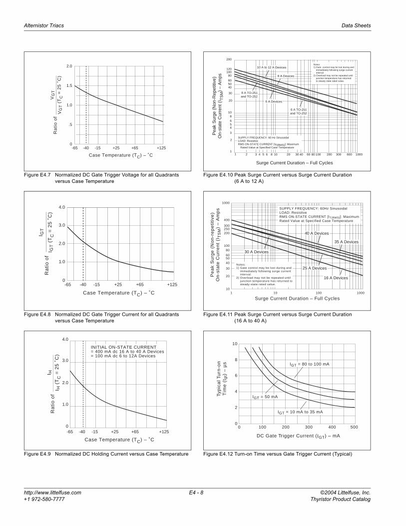
Figure E4.7 Normalized DC Gate Trigger Voltage for all Quadrants versus Case Temperature
Figure E4.8 Normalized DC Gate Trigger Current for all Quadrants versus Case Temperature
Figure E4.9 Normalized DC Holding Current versus Case Temperature
Figure E4.10 Peak Surge Current versus Surge Current Duration(6 A to 12 A)
Figure E4.11 Peak Surge Current versus Surge Current Duration(16 A to 40 A)
Figure E4.12 Turn-on Time versus Gate Trigger Current (Typical)
0
.5
1.0
1.5
2.0
-65 -15 +65+25 +125-40
Case Temperature (TC) – ˚C
VG
T (
TC
= 2
5 ˚
C)
Ra
tio
of
VG
T
0
1.0
2.0
3.0
4.0
-65 -15 +65+25 +125-40
Case Temperature (TC) – ˚C
I GT
(T
C =
25
˚C
)R
ati
o o
fI G
T
0
1.0
2.0
3.0
4.0
-65 -15 +65+25 +125-40
Case Temperature (TC) – ˚C
I H (
TC
= 2
5 ˚
C)
Ra
tio
of
I H
INITIAL ON-STATE CURRENT= 400 mA dc 16 A to 40 A Devices= 100 mA dc 6 to 12A Devices
200
120
40
1 2 3 4 5 6 8 10 20 30 40 60 80 100 200 300 600 1000
80
6050
100
8
65
10
30
20
4
1
3
2
Surge Current Duration – Full Cycles
Pea
k S
urge
(N
on-R
epet
itive
)O
n-st
ate
Cur
rent
(I T
SM
) –
Am
ps
SUPPLY FREQUENCY: 60 Hz SinusoidalLOAD: ResistiveRMS ON-STATE CURRENT [IT(RMS)]: Maximum Rated Value at Specified Case Temperature
Notes:1) Gate control may be lost during and immediately following surge current interval2) Overload may not be repeated until junction temperature has returned to steady state rated value.
10 A to 12 A Devices
8 A TO-251and TO-252
8 A Devices
6 A Devices
6 A TO-251and TO-252
1 10 100 100010
20
30
40
5060
80100
250300
400
1000
Surge Current Duration – Full Cycles
Pe
ak
Su
rge
(N
on
-re
pe
titi
ve)
On
-sta
te C
urr
en
t (I
TS
M)
– A
mp
s
200
Notes:1) Gate control may be lost during and immediately following surge current interval.2) Overload may not be repeated until junction temperature has returned to steady-state rated value.
SUPPLY FREQUENCY: 60Hz SinusoidalLOAD: ResistiveRMS ON-STATE CURRENT [IT(RMS)]: MaximumRated Value at Specified Case Temperature
40 A Devices
35 A Devices
30 A Devices
25 A Devices
16 A Devices
0 100 200 300 400 5000
2
4
6
8
10
DC Gate Trigger Current (IGT) – mA
IGT = 80 to 100 mA
Typ
ica
l Tu
rn-o
nT
ime
(t g
t) –
µs
IGT = 10 mA to 35 mA
IGT = 50 mA
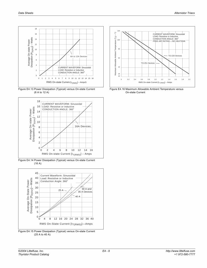
Data Sheets Alternistor Triacs
©2004 Littelfuse, Inc. E4 - 9 http://www.littelfuse.comThyristor Product Catalog +1 972-580-7777
Figure E4.13 Power Dissipation (Typical) versus On-state Current(6 A to 12 A)
Figure E4.14 Power Dissipation (Typical) versus On-state Current(16 A)
Figure E4.15 Power Dissipation (Typical) versus On-state Current(25 A to 40 A)
Figure E4.16 Maximum Allowable Ambient Temperature versus On-state Current
0 1 2 3 4 5 6 7 8 9 10 11 12 13 14 15 16
0
2
4
6
8
10
12
14
16
18
RMS On-state Current [lT(RMS)] – AmpsS
Ave
rage
On-
stat
e P
ower
Dis
sipa
tion
[PD
(AV
)] –
Wat
ts
CURRENT WAVEFORM: SinusoidalLOAD: Resistive or InductiveCONDUCTION ANGLE: 360˚
6A to 12A Devices
0 2 4 6 8 10 12 14 160
2
4
6
8
10
12
14
16
18
RMS On-state Current [IT(RMS)] – Amps
Ave
rag
e O
n-s
tate
Po
we
rD
issi
pa
tio
n [
PD
(AV
)] –
Wa
tts
CURRENT WAVEFORM: SinusoidalLOAD: Resistive or inductiveCONDUCTION ANGLE: 360˚
16A Devices
0 12 20 28 364 16 24 32 4080
5
10
15
20
25
30
35
40
45
RMS On-State Current [IT(RMS)]—Amps
Ave
rag
e O
n-S
tate
Po
we
rD
issi
pa
tio
n [
PD
(AV
)]—
Wa
tts
25 A
40 A
Current Waveform: Sinusoidal Load: Resistive or InductiveConduction Angle: 360˚
30 A and 35 A Devices
120
100
80
60
40
25
20
0 0.2 0.4 0.6 0.8 1.0 1.2 1.4 1.6 1.8 2.0
TO-220 Devices
RMS On-state Current [IT (RMS)] – Amps
Max
imum
Allo
wab
le A
mbi
ent T
empe
ratu
re (
TA)
– ˚C CURRENT WAVEFORM: Sinusoidal
LOAD: Resistive or InductiveCONDUCTION ANGLE: 360˚ FREE AIR RATING – NO HEATSINK
TO-251 Devices

Notes
©2004 Littelfuse, Inc. E5 - 1 http://www.littelfuse.comThyristor Product Catalog +1 972-580-7777
* Selecte
d Pack
ages
U.L
. RECO
GNIZ
ED
File #E
7163
9
SensitiveSCRs
(0.8 A to 10 A)
E5General DescriptionThe Teccor line of sensitive SCR semiconductors are half-wave unidirectional, gate-controlled rectifiers (SCR-thyristor) which complement Teccor's line of power SCRs. This group of packages offers ratings of 0.8 A to 10 A, and 200 V to 600 V with gate sensitivities of 12 µA to 500 µA. For gate currents in the 10 mA to 50 mA ranges, see “SCRs” section of this catalog.The TO-220 and TO-92 are electrically isolated where the case or tab is internally isolated to allow the use of low-cost assembly and convenient packaging techniques.Teccor's line of SCRs features glass-passivated junctions to ensure long-term device reliability and parameter stability. Teccor's glass offers a rugged, reliable barrier against junction contamination.Tape-and-reel packaging is available for the TO-92 package. Consult the factory for more information.Variations of devices covered in this data sheet are available for custom design applications. Consult the factory for more information.
Features• Electrically-isolated TO-220 package• High voltage capability — up to 600 V• High surge capability — up to 100 A• Glass-passivated chip
Compak Features• Surface mount package — 0.8 A series• New small-profile three-leaded Compak package• Four gate sensitivities available• Packaged in embossed carrier tape with 2,500
devices per reel• Can replace SOT-223
E5
TO-202
TO-92
3-leadCompak
*TO-220Isolated
TO-252D-Pak
TO-251V-Pak
A K
G

Sensitive SCRs Data Sheets
http://www.littelfuse.com E5 - 2 ©2004 Littelfuse, Inc.+1 972-580-7777 Thyristor Product Catalog
See “General Notes” on page E5 - 4 and “Electrical Specifications Notes” on page E5 - 5
TYPE
Part NumberIT
VDRM &VRRM IGT
IDRM &IRRM VTMNon-isolated
TO-92 TO-202TO-251V-Pak Compak
TO-252D-Pak
(1)
Amps
Volts
(2) (12) (14) (18)
µAmps
(20) (21)
µAmps
(3) (10)
VoltsSee “Package Dimensions” section for variations. (11)
IT(RMS) IT(AV)
TC or TL =25 °C
TC or TL =100 °C
TC or TL =110 °C
MAX MIN MAX MAX MAX
0.8 A
S2S1 0.8 0.51 200 12 2 100 1.7S4S1 0.8 0.51 400 12 2 100 1.7S6S1 0.8 0.51 600 12 2 100 1.7S2S2 0.8 0.51 200 50 2 100 1.7S4S2 0.8 0.51 400 50 2 100 1.7S6S2 0.8 0.51 600 50 2 100 1.7S2S 0.8 0.51 200 200 2 100 1.7S4S 0.8 0.51 400 200 2 100 1.7S6S 0.8 0.51 600 200 2 100 1.7
S2S3 0.8 0.51 200 500 2 100 1.7S4S3 0.8 0.51 400 500 2 100 1.7S6S3 0.8 0.51 600 500 2 100 1.7
EC103B 0.8 0.51 200 200 1 50 1.7EC103D 0.8 0.51 400 200 1 50 1.7EC103M 0.8 0.51 600 200 2 100 1.7EC103B1 0.8 0.51 200 12 1 50 1.7EC103D1 0.8 0.51 400 12 1 50 1.7EC103M1 0.8 0.51 600 12 2 100 1.7EC103B2 0.8 0.51 200 50 1 50 1.7EC103D2 0.8 0.51 400 50 1 50 1.7EC103M2 0.8 0.51 600 50 2 100 1.7EC103B3 0.8 0.51 200 500 1 50 1.7EC103D3 0.8 0.51 400 500 1 50 1.7EC103M3 0.8 0.51 600 500 2 100 1.72N5064 0.8 0.51 200 200 1 50 1.72N6565 0.8 0.51 400 200 1 100 1.7
1.5 ATCR22-4 1.5 0.95 200 200 1 100 1.5TCR22-6 1.5 0.95 400 200 1 100 1.5TCR22-8 1.5 0.95 600 200 2 100 1.5
4 A
T106B1 4 2.5 200 200 2 100 2.2T106D1 4 2.5 400 200 2 100 2.2T106M1 4 2.5 600 200 2 100 2.2T107B1 4 2.5 200 500 2 100 2.5T107D1 4 2.5 400 500 2 100 2.5T107M1 4 2.5 600 500 2 100 2.5
S2004VS1 S2004DS1 4 2.5 200 50 2 100 1.6S4004VS1 S4004DS1 4 2.5 400 50 2 100 1.6S6004VS1 S6004DS1 4 2.5 600 50 2 100 1.6S2004VS2 S2004DS2 4 2.5 200 200 2 100 1.6S4004VS2 S4004DS2 4 2.5 400 200 2 100 1.6S6004VS2 S6004DS2 4 2.5 600 200 2 100 1.6
KG
AK
AG
A A
AG
K
A
G
K
A
A
K
G
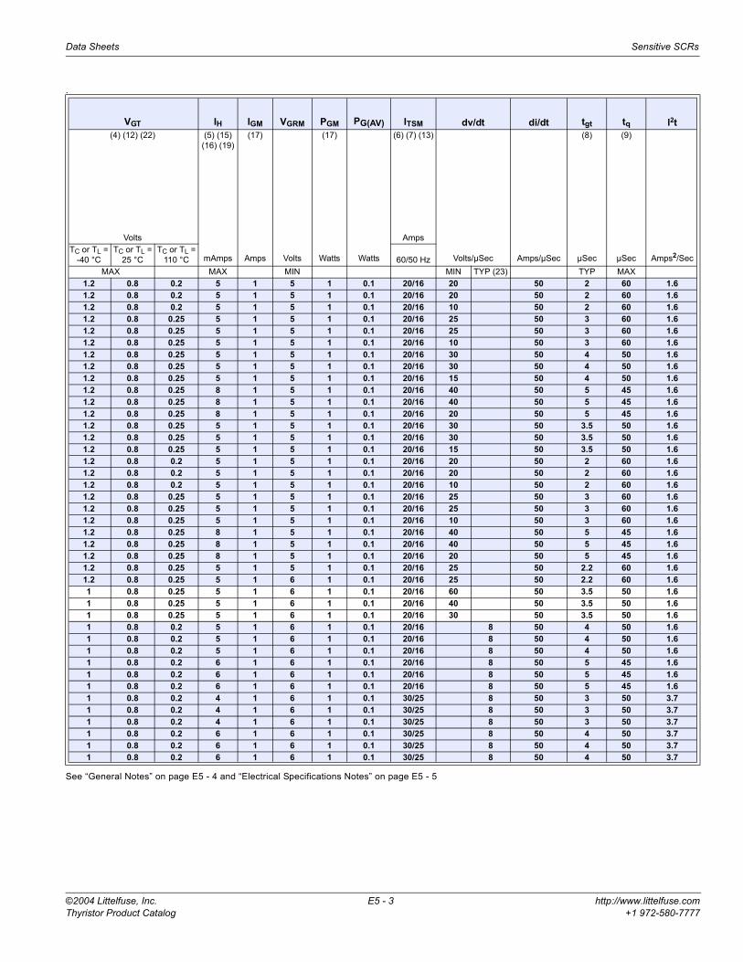
Data Sheets Sensitive SCRs
©2004 Littelfuse, Inc. E5 - 3 http://www.littelfuse.comThyristor Product Catalog +1 972-580-7777
.
See “General Notes” on page E5 - 4 and “Electrical Specifications Notes” on page E5 - 5
VGT IH IGM VGRM PGM PG(AV) ITSM dv/dt di/dt tgt tq l2t(4) (12) (22)
Volts
(5) (15)(16) (19)
mAmps
(17)
Amps Volts
(17)
Watts Watts
(6) (7) (13)
Amps
Volts/µSec Amps/µSec
(8)
µSec
(9)
µSec Amps2/SecTC or TL =
-40 °CTC or TL =
25 °CTC or TL =
110 °C 60/50 HzMAX MAX MIN MIN TYP (23) TYP MAX
1.2 0.8 0.2 5 1 5 1 0.1 20/16 20 50 2 60 1.61.2 0.8 0.2 5 1 5 1 0.1 20/16 20 50 2 60 1.61.2 0.8 0.2 5 1 5 1 0.1 20/16 10 50 2 60 1.61.2 0.8 0.25 5 1 5 1 0.1 20/16 25 50 3 60 1.61.2 0.8 0.25 5 1 5 1 0.1 20/16 25 50 3 60 1.61.2 0.8 0.25 5 1 5 1 0.1 20/16 10 50 3 60 1.61.2 0.8 0.25 5 1 5 1 0.1 20/16 30 50 4 50 1.61.2 0.8 0.25 5 1 5 1 0.1 20/16 30 50 4 50 1.61.2 0.8 0.25 5 1 5 1 0.1 20/16 15 50 4 50 1.61.2 0.8 0.25 8 1 5 1 0.1 20/16 40 50 5 45 1.61.2 0.8 0.25 8 1 5 1 0.1 20/16 40 50 5 45 1.61.2 0.8 0.25 8 1 5 1 0.1 20/16 20 50 5 45 1.61.2 0.8 0.25 5 1 5 1 0.1 20/16 30 50 3.5 50 1.61.2 0.8 0.25 5 1 5 1 0.1 20/16 30 50 3.5 50 1.61.2 0.8 0.25 5 1 5 1 0.1 20/16 15 50 3.5 50 1.61.2 0.8 0.2 5 1 5 1 0.1 20/16 20 50 2 60 1.61.2 0.8 0.2 5 1 5 1 0.1 20/16 20 50 2 60 1.61.2 0.8 0.2 5 1 5 1 0.1 20/16 10 50 2 60 1.61.2 0.8 0.25 5 1 5 1 0.1 20/16 25 50 3 60 1.61.2 0.8 0.25 5 1 5 1 0.1 20/16 25 50 3 60 1.61.2 0.8 0.25 5 1 5 1 0.1 20/16 10 50 3 60 1.61.2 0.8 0.25 8 1 5 1 0.1 20/16 40 50 5 45 1.61.2 0.8 0.25 8 1 5 1 0.1 20/16 40 50 5 45 1.61.2 0.8 0.25 8 1 5 1 0.1 20/16 20 50 5 45 1.61.2 0.8 0.25 5 1 5 1 0.1 20/16 25 50 2.2 60 1.61.2 0.8 0.25 5 1 6 1 0.1 20/16 25 50 2.2 60 1.61 0.8 0.25 5 1 6 1 0.1 20/16 60 50 3.5 50 1.61 0.8 0.25 5 1 6 1 0.1 20/16 40 50 3.5 50 1.61 0.8 0.25 5 1 6 1 0.1 20/16 30 50 3.5 50 1.61 0.8 0.2 5 1 6 1 0.1 20/16 8 50 4 50 1.61 0.8 0.2 5 1 6 1 0.1 20/16 8 50 4 50 1.61 0.8 0.2 5 1 6 1 0.1 20/16 8 50 4 50 1.61 0.8 0.2 6 1 6 1 0.1 20/16 8 50 5 45 1.61 0.8 0.2 6 1 6 1 0.1 20/16 8 50 5 45 1.61 0.8 0.2 6 1 6 1 0.1 20/16 8 50 5 45 1.61 0.8 0.2 4 1 6 1 0.1 30/25 8 50 3 50 3.71 0.8 0.2 4 1 6 1 0.1 30/25 8 50 3 50 3.71 0.8 0.2 4 1 6 1 0.1 30/25 8 50 3 50 3.71 0.8 0.2 6 1 6 1 0.1 30/25 8 50 4 50 3.71 0.8 0.2 6 1 6 1 0.1 30/25 8 50 4 50 3.71 0.8 0.2 6 1 6 1 0.1 30/25 8 50 4 50 3.7

Sensitive SCRs Data Sheets
http://www.littelfuse.com E5 - 4 ©2004 Littelfuse, Inc.+1 972-580-7777 Thyristor Product Catalog
Specific Test Conditionsdi/dt — Maximum rate-of-change of on-state current; IGT = 50 mA pulse
width ≥15 µsec with ≤0.1 µs rise timedv/dt — Critical rate-of-rise of forward off-state voltageI2t — RMS surge (non-repetitive) on-state current for period of 8.3 ms
for fusingIDRM and IRRM — Peak off-state current at VDRM and VRRM
IGT — DC gate trigger current VD = 6 V dc; RL = 100 ΩIGM — Peak gate currentIH — DC holding current; initial on-state current = 20 mAIT — Maximum on-state currentITSM — Peak one-cycle forward surge currentPG(AV) — Average gate power dissipationPGM — Peak gate power dissipationtgt — Gate controlled turn-on time gate pulse = 10 mA; minimum
width = 15 µS with rise time ≤0.1 µstq — Circuit commutated turn-off timeVDRM and VRRM — Repetitive peak off-state forward and reverse voltageVGRM — Peak reverse gate voltageVGT — DC gate trigger voltage; VD = 6 V dc; RL = 100 ΩVTM — Peak on-state voltage
General Notes• Teccor 2N5064 and 2N6565 Series devices conform to all JEDEC
registered data. See specifications table on pages E5 - 2 andE5 - 3.
• The case lead temperature (TC or TL) is measured as shown on dimensional outline drawings in the “Package Dimensions” section of this catalog.
• All measurements (except IGT) are made with an external resistor RGK = 1 kΩ unless otherwise noted.
• All measurements are made at 60 Hz with a resistive load at an ambient temperature of +25 °C unless otherwise specified.
• Operating temperature (TJ) is -65 °C to +110 °C for EC Series devices, -65 °C to +125 °C for 2N Series devices, -40 °C to +125 °C for “TCR” Series, and -40 °C to +110 °C for all others.
• Storage temperature range (TS) is -65 °C to +150 °C for TO-92 devices, -40 °C to +150 °C for TO-202 and Compak devices, and-40 °C to +125 °C for all others.
• Lead solder temperature is a maximum of +230 °C for 10 seconds maximum ≥1/16" (1.59 mm) from case.
TYPE
Part NumberIT
VDRM &VRRM IGT
IDRM &IRRM VTMIsolated Non-isolated
TO-220 TO-202TO-251V-Pak
TO-252D-Pak
(1)
Amps
Volts
(2) (12)
µAmps
(20) (21)
µAmps
(3) (10)
VoltsSee “Package Dimensions” section for variations. (11)
IT(RMS) IT(AV)TC =25 °C
TC =110 °C
MAX MAX MIN MAX MAX MAX MAX
6 A
S2006LS2 S2006FS21 S2006VS2 S2006DS2 6 3.8 200 200 5 250 1.6S4006LS2 S4006FS21 S4006VS2 S4006DS2 6 3.8 400 200 5 250 1.6S6006LS2 S6006FS21 S6006VS2 S6006DS2 6 3.8 600 200 5 250 1.6S2006LS3 S2006FS31 S2006VS3 S2006DS3 6 3.8 200 500 5 250 1.6S4006LS3 S4006FS31 S4006VS3 S4006DS3 6 3.8 400 500 5 250 1.6S6006LS3 S6006FS31 S6006VS3 S6006DS3 6 3.8 600 500 5 250 1.6
8 A
S2008LS2 S2008FS21 S2008VS2 S2008DS2 8 5.1 200 200 5 250 1.6S4008LS2 S4008FS21 S4008VS2 S4008DS2 8 5.1 400 200 5 250 1.6S6008LS2 S6008FS21 S6008VS2 S6008DS2 8 5.1 600 200 5 250 1.6S2008LS3 S2008FS31 S2008VS3 S2008DS3 8 5.1 200 500 5 250 1.6S4008LS3 S4008FS31 S4008VS3 S4008DS3 8 5.1 400 500 5 250 1.6S6008LS3 S6008FS31 S6008VS3 S6008DS3 8 5.1 600 500 5 250 1.6
10 A
S2010LS2 S2010FS21 S2010VS2 S2010DS2 10 6.4 200 200 5 250 1.6S4010LS2 S4010FS21 S4010VS2 S4010DS2 10 6.4 400 200 5 250 1.6S6010LS2 S6010FS21 S6010VS2 S6010DS2 10 6.4 600 200 5 250 1.6S2010LS3 S2010FS31 S2010VS3 S2010DS3 10 6.4 200 500 5 250 1.6S4010LS3 S4010FS31 S4010VS3 S4010DS3 10 6.4 400 500 5 250 1.6S6010LS3 S6010FS31 S6010VS3 S6010DS3 10 6.4 600 500 5 250 1.6
KA
G KA
G
A A
AG
K
A
A
K
G

Data Sheets Sensitive SCRs
©2004 Littelfuse, Inc. E5 - 5 http://www.littelfuse.comThyristor Product Catalog +1 972-580-7777
Electrical Specifications Notes(1) See Figure E5.1 through Figure E5.9 for current ratings at
specified operating temperatures.(2) See Figure E5.10 for IGT versus TC or TL.(3) See Figure E5.11 for instantaneous on-state current (iT) versus on-
state voltage (vT) TYP.(4) See Figure E5.12 for VGT versus TC or TL.(5) See Figure E5.13 for IH versus TC or TL.(6) For more than one full cycle, see Figure E5.14.(7) 0.8 A to 4 A devices also have a pulse peak forward current on-
state rating (repetitive) of 75 A. This rating applies for operation at 60 Hz, 75 °C maximum tab (or anode) lead temperature, switching from 80 V peak, sinusoidal current pulse width of 10 µs minimum, 15 µs maximum. See Figure E5.20 and Figure E5.21.
(8) See Figure E5.15 for tgt versus IGT.(9) Test conditions as follows:
– TC or TL ≤80 °C, rectangular current waveform– Rate-of-rise of current ≤10 A/µs– Rate-of-reversal of current ≤5 A/µs– ITM = 1 A (50 µs pulse), Repetition Rate = 60 pps– VRRM = Rated– VR = 15 V minimum, VDRM = Rated– Rate-of-rise reapplied forward blocking voltage = 5 V/µs– Gate Bias = 0 V, 100 Ω (during turn-off time interval)
(10) Test condition is maximum rated RMS current except TO-92 devices are 1.2 APK; T106/T107 devices are 4 APK.
(11) See package outlines for lead form configurations. When ordering special lead forming, add type number as suffix to part number.
(12) VD = 6 V dc, RL = 100 Ω (See Figure E5.19 for simple test circuit for measuring gate trigger voltage and gate trigger current.)
(13) See Figure E5.1 through Figure E5.9 for maximum allowable case temperature at maximum rated current.
(14) IGT = 500 µA maximum at TC = -40 °C for T106 devices(15) IH = 10 mA maximum at TC = -65 °C for 2N5064 Series and
2N6565 Series devices(16) IH = 6 mA maximum at TC = -40 °C for T106 devices(17) Pulse Width ≤10 µs(18) IGT = 350 µA maximum at TC = -65 °C for 2N5064 Series and
2N6565 Series devices(19) Latching current can be higher than 20 mA for higher IGT types.
Also, latching current can be much higher at -40 °C. See Figure E5.18.
(20) TC or TL = TJ for test conditions in off state(21) IDRM and IRRM = 50 µA for 2N5064 and 100 µA for 2N6565 at
125 °C(22) TO-92 devices specified at -65 °C instead of -40 °C(23) TC = 110 °C
VGT IH IGM VGRM PGM PG(AV) ITSM dv/dt di/dt tgt tq l2t(4) (12) (22)
Volts
(5) (19)
mAmps
(17)
Amps Volts
(17)
Watts Watts
(6) (13)
Amps
Volts/µSec
Amps/µSec
(8)
µSec
(9)
µSec Amps2SecTC =
-40 °CTC =25 °C
TC =110 °C TC = 110 °C
MAX MAX MIN 60/50 Hz TYP TYP MAX1 0.8 0.25 6 1 6 1 0.1 100/83 10 100 4 50 411 0.8 0.25 6 1 6 1 0.1 100/83 8 100 4 50 411 0.8 0.25 6 1 6 1 0.1 100/83 8 100 4 50 411 0.8 0.25 8 1 6 1 0.1 100/83 10 100 5 45 411 0.8 0.25 8 1 6 1 0.1 100/83 8 100 5 45 411 0.8 0.25 8 1 6 1 0.1 100/83 8 100 5 45 411 0.8 0.25 6 1 6 1 0.1 100/83 10 100 4 50 411 0.8 0.25 6 1 6 1 0.1 100/83 8 100 4 50 411 0.8 0.25 6 1 6 1 0.1 100/83 8 100 4 50 411 0.8 0.25 8 1 6 1 0.1 100/83 10 100 5 45 411 0.8 0.25 8 1 6 1 0.1 100/83 8 100 5 45 411 0.8 0.25 8 1 6 1 0.1 100/83 8 100 5 45 411 0.8 0.25 6 1 6 1 0.1 100/83 10 100 4 50 411 0.8 0.25 6 1 6 1 0.1 100/83 8 100 4 50 411 0.8 0.25 6 1 6 1 0.1 100/83 8 100 4 50 411 0.8 0.25 8 1 6 1 0.1 100/83 10 100 5 45 411 0.8 0.25 8 1 6 1 0.1 100/83 8 100 5 45 411 0.8 0.25 8 1 6 1 0.1 100/83 8 100 5 45 41
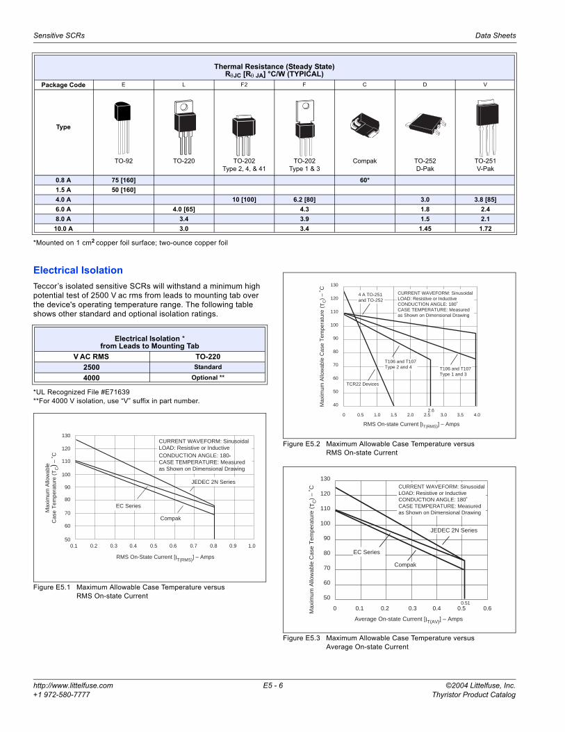
Sensitive SCRs Data Sheets
http://www.littelfuse.com E5 - 6 ©2004 Littelfuse, Inc.+1 972-580-7777 Thyristor Product Catalog
*Mounted on 1 cm2 copper foil surface; two-ounce copper foil
Electrical IsolationTeccor’s isolated sensitive SCRs will withstand a minimum high potential test of 2500 V ac rms from leads to mounting tab over the device's operating temperature range. The following table shows other standard and optional isolation ratings.
*UL Recognized File #E71639**For 4000 V isolation, use “V” suffix in part number.
Figure E5.1 Maximum Allowable Case Temperature versus RMS On-state Current
Figure E5.2 Maximum Allowable Case Temperature versus RMS On-state Current
Figure E5.3 Maximum Allowable Case Temperature versus Average On-state Current
Thermal Resistance (Steady State)RθJC [Rθ JA] °C/W (TYPICAL)
Package Code E L F2 F C D V
Type
TO-92 TO-220 TO-202Type 2, 4, & 41
TO-202Type 1 & 3
Compak TO-252D-Pak
TO-251V-Pak
0.8 A 75 [160] 60*1.5 A 50 [160]4.0 A 10 [100] 6.2 [80] 3.0 3.8 [85]6.0 A 4.0 [65] 4.3 1.8 2.48.0 A 3.4 3.9 1.5 2.110.0 A 3.0 3.4 1.45 1.72
Electrical Isolation *from Leads to Mounting Tab
V AC RMS TO-2202500 Standard
4000 Optional **
50
60
70
80
90
100
110
120
130CURRENT WAVEFORM: SinusoidalLOAD: Resistive or InductiveCONDUCTION ANGLE: 180˚CASE TEMPERATURE: Measuredas Shown on Dimensional Drawing
RMS On-State Current [IT(RMS)] – Amps
Max
imum
Allo
wab
leC
ase
Tem
pera
ture
(T
C) –
˚C
Compak
0.1 0.2 0.3 0.4 0.5 0.6 0.7 0.8 0.9 1.0
EC Series
JEDEC 2N Series
0 0.5 1.0 1.5 2.0 2.5 3.0 3.5 4.0
40
50
60
70
80
90
100
110
120
130
CURRENT WAVEFORM: SinusoidalLOAD: Resistive or InductiveCONDUCTION ANGLE: 180˚CASE TEMPERATURE: Measuredas Shown on Dimensional Drawing
RMS On-state Current [IT(RMS)] – Amps
Max
imum
Allo
wab
le C
ase
Tem
pera
ture
(T
C)
– ˚C
2.6
4 A TO-251and TO-252
T106 and T107Type 1 and 3
T106 and T107Type 2 and 4
TCR22 Devices
0 0.1 0.2 0.3 0.4 0.5 0.6
50
60
70
80
90
100
110
120
130CURRENT WAVEFORM: SinusoidalLOAD: Resistive or InductiveCONDUCTION ANGLE: 180˚CASE TEMPERATURE: Measuredas Shown on Dimensional Drawing
Average On-state Current [IT(AV)] – Amps
Max
imum
Allo
wab
le C
ase
Tem
pera
ture
(T
C)
– ˚C
0.51
Compak
EC Series
JEDEC 2N Series

Data Sheets Sensitive SCRs
©2004 Littelfuse, Inc. E5 - 7 http://www.littelfuse.comThyristor Product Catalog +1 972-580-7777
Figure E5.4 Maximum Allowable Case Temperature versus Average On-state Current
Figure E5.5 Maximum Allowable Ambient Temperature versus On-state Current
Figure E5.6 Maximum Allowable Ambient Temperature versus RMS On-state Current
Figure E5.7 Maximum Allowable Ambient Temperature versus Average On-state Current
Figure E5.8 Maximum Allowable Case Temperature versus RMS On-state Current
Figure E5.9 Maximum Allowable Case Temperature versus Average On-state Current
0 0.5 1.0 1.5 2.0 2.5 3.0
50
60
70
80
90
100
110
120
130
Average On-state Current [IT(AV)] – Amps
Max
imum
Allo
wab
leC
ase
Tem
pera
ture
(T
C)
– ˚C
0.9540
CURRENT WAVEFORM: SinusoidalLOAD: Resistive or InductiveCONDUCTION ANGLE: 180˚CASE TEMPERATURE: Measuredas Shown on Dimensional Drawing
1.65 1.9 2.54
T106 and T107Type 1 and 3
T106 and T107Type 2 and 4
TCR22Devices
0 0.1 0.2 0.3 0.4 0.5 0.6 0.7 0.8 0.9
140
120
100
80
60
40
20
CURRENT WAVEFORM: SinusoidalLOAD: Resistive or InductiveCONDUCTION ANGLE: 180˚FREE AIR RATING
1.5 A and JEDEC2N Series IT(AV)
and EC Series IT(AV)
On-state Current – Amps
Max
imum
Allo
wab
le A
mbi
ent T
empe
ratu
re (
TA)
– ˚C
1.5 A Devicesand JEDEC2N Series IT(RMS)
EC Series IT(RMS)
0 0.2 0.4 0.6 0.8 1.0 1.2 1.4 1.6 1.8
140
120
100
80
60
40
20
RMS On-state Current [IT(RMS)] – Amps
Max
imum
Allo
wab
leA
mbi
ent T
empe
ratu
re (
TA
) –
˚C
2.0
CURRENT WAVEFORM: SinusoidalLOAD: Resistive or InductiveCONDUCTION ANGLE: 180˚FREE AIR RATING
TO-220
T106/T107 TO-202Type 1 and 3
T106/T107 TO-202Type 2 and 4and TO-251
0 0.2 0.4 0.6 0.8 1.0 1.2 1.4
20
40
60
80
100
120
140CURRENT WAVEFORM: SinusoidalLOAD: Resistive or InductiveCONDUCTION ANGLE: 180˚FREE AIR RATING
Average On-state Current [IT(AV)] – Amps
Max
imum
Allo
wab
leA
mbi
ent T
empe
ratu
re (
TA)
– ˚C
TO-220
T106/T107 TO-202Type 1 and 3
T106/T107 TO-202Type 2 and 4and TO-251
80
2 4 6 8 100
85
90
95
100
105
110
115CURRENT WAVEFORM: SinusoidalLOAD: Resistive or InductiveCONDUCTION ANGLE: 180˚TEMPERATURE: Measured asShown on Dimensional Drawings
RMS On-state Current [IT(RMS)] – Amps
Max
imum
Allo
wab
leC
ase
Tem
pera
ture
(T
C)
– ˚C
6 A TO-220and TO-202
8 A TO-220and TO-202
10 A TO-220and TO-202
6 A TO-251and TO-252
8 A TO-251and TO-252
10 A TO-251and TO-252
80
1 3 4 5 60
85
90
95
100
105
110
Average On-state Current [IT(AV)] – Amps
Max
imum
Allo
wab
leC
ase
Tem
pera
ture
(T
C)
– ˚C
72
CURRENT WAVEFORM: SinusoidalLOAD: Resistive or InductiveCONDUCTION ANGLE: 180˚CASE TEMPERATURE: Measuredas Shown on Dimensional Drawings
6 A TO-220and TO-202
8 A TO-220and TO-202
10 A TO-220and TO-202
6 A TO-251and TO-252
8 A TO-251and TO-252
10 A TO-251and TO-252

Sensitive SCRs Data Sheets
http://www.littelfuse.com E5 - 8 ©2004 Littelfuse, Inc.+1 972-580-7777 Thyristor Product Catalog
Figure E5.10 Normalized DC Gate-Trigger Current versus Case Temperature
Figure E5.11 Instantaneous On-state Current versus On-state Voltage (Typical)
Figure E5.12 Normalized DC Gate-Trigger Voltage versusCase Temperature
Figure E5.13 Normalized DC Holding Current versus Case Temperature
-65 -15 +25 +65 +110 +125-40
0
1.0
2.0
3.0
4.0
5.0
6.0
7.0
8.0
9.0
Case Temperature (TC) – ˚C
Rat
io o
fI G
T
I GT (
TC
= 2
5 ˚C
)
See General Notes for specific deviceoperating temperature range.
0 .6 .8 1.0 1.2 1.4 1.6
0
4
8
12
16
20
24
28
32
TC = 25˚C
6 A to 10 A Devices
0.8 A to 1.5 A TO-92, T106/T107, andCompak
Instantaneous On-state Voltage (vT) – Volts
Inst
anta
neou
s O
n-st
ate
Cur
rent
(i T
) –
Am
ps
4 A TO-251 and TO-252
-65 -15 +25 +65 +110 +125-40
0
0.5
1.0
1.5
2.0
Case Temperature (TC) – ˚C
Rat
io o
fV
GT
VG
T (
TC
= 2
5 C
)
See General Notes for specificoperating temperature range
-65 -40 -15 +25 +65 +110 +125
0
1.0
2.0
3.0
4.0
See General Notes for specificoperating temperature range.
Case Temperature (TC) – ˚C
Ratio
of
I HI H
(TC
= 2
5 ˚
C)
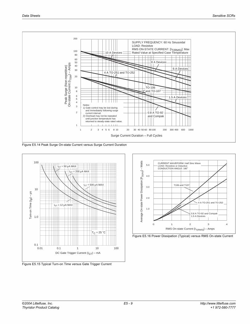
Data Sheets Sensitive SCRs
©2004 Littelfuse, Inc. E5 - 9 http://www.littelfuse.comThyristor Product Catalog +1 972-580-7777
Figure E5.14 Peak Surge On-state Current versus Surge Current Duration
Figure E5.15 Typical Turn-on Time versus Gate Trigger Current
Figure E5.16 Power Dissipation (Typical) versus RMS On-state Current
1 2 3 4 5 6 8 10 20 30 40 50 60 80 100 200 300 400 600 1000
1
2
3
456
8
10
20
30
40
5060
80
100
200
SUPPLY FREQUENCY: 60 Hz SinusoidalLOAD: ResistiveRMS ON-STATE CURRENT: [IT(RMS)]: MaxRated Value at Specified Case Temperature
Surge Current Duration – Full Cycles
Pea
k S
urge
(N
on-r
epet
itive
)O
n-st
ate
Cur
rent
(I T
SM
) –
Am
ps
Notes:1) Gate control may be lost during and immediately following surge current interval.2) Overload may not be repeated until junction temperature has returned to steady-state rated value.
6 A Devices
8 A Devices
10 A Devices
4 A TO-251 and TO-252
1.5 A Devices
TO-106and TO-107
0.8 A TO-92and Compak
0.01 0.1 1 10 1000.1
1.0
10
100IGT = 50 µA MAX
IGT = 200 µA MAX
IGT = 500 µA MAX
TC = 25 ˚C
IGT = 12 µA MAX
DC Gate Trigger Current (IGT) – mA
Tur
n-on
Tim
e (t
gt)
– µs
0 1 2 3 4
1.0
2.0
3.0
4.0
5.0
T106 and T107
0.8 A TO-92 and Compak1.5 A Devices
RMS On-state Current [IT(RMS)] – Amps
Ave
rage
On-
stat
e P
ower
Dis
sipa
tion
[PD
(AV
)] –
Wat
ts
CURRENT WAVEFORM: Half Sine WaveLOAD: Resistive or InductiveCONDUCTION ANGLE: 180˚
4 A TO-251 and TO-252
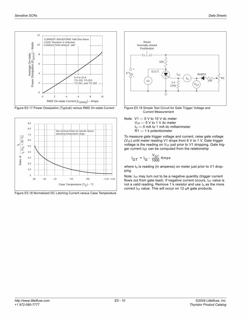
Sensitive SCRs Data Sheets
http://www.littelfuse.com E5 - 10 ©2004 Littelfuse, Inc.+1 972-580-7777 Thyristor Product Catalog
Figure E5.17 Power Dissipation (Typical) versus RMS On-state Current
Figure E5.18 Normalized DC Latching Current versus Case Temperature
Figure E5.19 Simple Test Circuit for Gate Trigger Voltage andCurrent Measurement
Note: V1 — 0 V to 10 V dc meterVGT — 0 V to 1 V dc meterIG — 0 mA to 1 mA dc milliammeterR1 — 1 k potentiometer
To measure gate trigger voltage and current, raise gate voltage (VGT) until meter reading V1 drops from 6 V to 1 V. Gate trigger voltage is the reading on VGT just prior to V1 dropping. Gate trig-ger current IGT can be computed from the relationship
where IG is reading (in amperes) on meter just prior to V1 drop-ping.Note: IGT may turn out to be a negative quantity (trigger current flows out from gate lead). If negative current occurs, IGT value is not a valid reading. Remove 1 k resistor and use IG as the more correct IGT value. This will occur on 12 µA gate products.
0 2 4 6 8 10
0
2
4
6
8
10
12
RMS On-state Current [IT(RMS)] – Amps
CURRENT WAVEFORM: Half Sine WaveLOAD: Resistive or InductiveCONDUCTION ANGLE: 180˚
Ave
rage
On-
stat
eP
ower
Dis
sipa
tion
[PD
(AV
)] –
Wat
ts
6 A to 10 ATO-220, TO-202,TO-251, and TO-252
-65 -15 +25 +65 +110 +125-40
0
1.0
2.0
3.0
4.0
5.0
6.0
7.0
8.0
9.0
Case Temperature (TC) – ˚C
Rat
io o
fI L
I L (
TC
= 2
5 ˚C
)
See General Notes for specific deviceoperating temperature range.
V1
6 VDC
+
–
100
D.U.T.
ResetNormally-closed
Pushbutton
1 k(1%)
IG
VGT
100
IGTR1
IN4001
IGT IGVGT1000------------- Amps–=
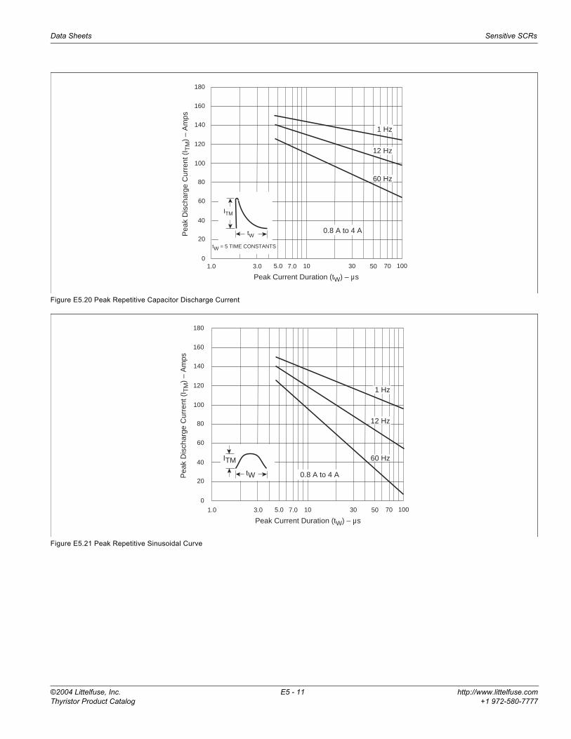
Data Sheets Sensitive SCRs
©2004 Littelfuse, Inc. E5 - 11 http://www.littelfuse.comThyristor Product Catalog +1 972-580-7777
Figure E5.20 Peak Repetitive Capacitor Discharge Current
Figure E5.21 Peak Repetitive Sinusoidal Curve
180
160
140
120
100
80
60
40
20
01.0 3.0 5.0 7.0 10 30 50 70 100
Pea
k D
isch
arge
Cur
rent
(I T
M)
– A
mps
Peak Current Duration (tW) – µs
0.8 A to 4 A
ITM
tW
tW = 5 TIME CONSTANTS
60 Hz
12 Hz
1 Hz
180
160
140
120
100
80
60
40
20
0
1.0 3.0 5.0 7.0 10 30 50 70 100
Pea
k D
isch
arge
Cur
rent
(I T
M)
– A
mps
Peak Current Duration (tW) – µs
0.8 A to 4 A
ITM
tW
60 Hz
12 Hz
1 Hz

Notes
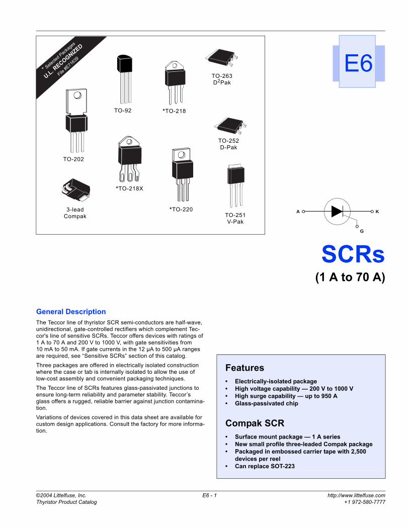
©2004 Littelfuse, Inc. E6 - 1 http://www.littelfuse.comThyristor Product Catalog +1 972-580-7777
* Selecte
d Pack
ages
U.L
. RECO
GNIZ
ED
File #E
7163
9
A K
G
SCRs(1 A to 70 A)
E6General DescriptionThe Teccor line of thyristor SCR semi-conductors are half-wave, unidirectional, gate-controlled rectifiers which complement Tec-cor's line of sensitive SCRs. Teccor offers devices with ratings of 1 A to 70 A and 200 V to 1000 V, with gate sensitivities from 10 mA to 50 mA. If gate currents in the 12 µA to 500 µA ranges are required, see “Sensitive SCRs” section of this catalog.Three packages are offered in electrically isolated construction where the case or tab is internally isolated to allow the use of low-cost assembly and convenient packaging techniques.The Teccor line of SCRs features glass-passivated junctions to ensure long-term reliability and parameter stability. Teccor’s glass offers a rugged, reliable barrier against junction contamina-tion.Variations of devices covered in this data sheet are available for custom design applications. Consult the factory for more informa-tion.
Features• Electrically-isolated package• High voltage capability — 200 V to 1000 V• High surge capability — up to 950 A• Glass-passivated chip
Compak SCR• Surface mount package — 1 A series• New small profile three-leaded Compak package• Packaged in embossed carrier tape with 2,500
devices per reel• Can replace SOT-223
E6
TO-92 *TO-218
TO-202
*TO-218X
3-leadCompak
TO-252D-Pak
TO-251V-Pak
*TO-220
TO-263D2Pak
SCRs Data Sheets
http://www.littelfuse.com E6 - 2 ©2004 Littelfuse, Inc.+1 972-580-7777 Thyristor Product Catalog
Specific Test Conditionsdi/dt — Maximum rate-of-rise of on-state current; IGT = 150 mA with
≤ 0.1 µs rise timedv/dt — Critical rate of applied forward voltageI2t — RMS surge (non-repetitive) on-state current for period of 8.3 ms
for fusingIDRM and IRRM — Peak off-state forward and reverse current at VDRM and
VRRM
Igt — dc gate trigger current; VD = 12 V dc; RL = 60 Ω for 1 to 16 A devices and 30 Ω for 20 to 70 A devices
IGM — Peak gate currentIH — dc holding current; gate openIT — Maximum on-state currentITSM — Peak one-cycle forward surge currentPG(AV) — Average gate power dissipationPGM — Peak gate power dissipationtgt — Gate controlled turn-on time; gate pulse = 100 mA; minimum
width = 15 µs with rise time ≤ 0.1 µstq — Circuit commutated turn-off time
VDRM and VRRM — Repetitive peak off-state forward and reverse voltageVgt — DC gate trigger voltage; VD = 12 V dc; RL = 60 Ω for 1 to 16 A
devices and 30 Ω for 20 to 70 A devicesVTM — Peak on-state voltage at maximum rated RMS current
General Notes• All measurements are made at 60 Hz with a resistive load at an
ambient temperature of +25 °C unless otherwise specified.• Operating temperature range (TJ) is -65 °C to +125 °C for TO-92
devices and -40 °C to +125 °C for all other packages.• Storage temperature range (TS) is -65 °C to +150 °C for TO-92
devices, -40 °C to +150 °C for TO-202 and TO-220 devices, and-40 °C to +125 °C for all others.
• Lead solder temperature is a maximum of 230 °C for 10 seconds maximum; ≥1/16" (1.59 mm) from case.
• The case temperature (TC) is measured as shown on dimensional outline drawings in the “Package Dimensions” sectionof this catalog.
TYPE
Part NumberIT
VDRM& VRRM IGTIsolated Non-isolated
TO-92 TO-220 TO-202 TO-220TO-251V-Pak Compak
TO-252D-Pak
(1) (2) (15)
AmpsVolts
(4)
mAmpsSee “Package Dimensions” section for variations. (11)
IT(RMS) IT(AV)
MAX MAX MIN MIN MAX
1 AS201E S2N1 1 0.64 200 1 10S401E S4N1 1 0.64 400 1 10S601E S6N1 1 0.64 600 1 10
6 A
S2006L S2006F1 S2006V S2006D 6 3.8 200 1 15S4006L S4006F1 S4006V S4006D 6 3.8 400 1 15S6006L S6006F1 S6006V S6006D 6 3.8 600 1 15S8006L S8006V S8006D 6 3.8 800 1 15SK006L SK006V SK006D 6 3.8 1000 1 15
8 A
S2008L S2008F1 S2008R S2008V S2008D 8 5.1 200 1 15S4008L S4008F1 S4008R S4008V S4008D 8 5.1 400 1 15S6008L S6008F1 S6008R S6008V S6008D 8 5.1 600 1 15S8008L S8008R S8008V S8008D 8 5.1 800 1 15SK008L SK008R SK008V SK008D 8 5.1 1000 1 15
10 A
S2010L S2010F1 S2010R S2010V S2010D 10 6.4 200 1 15S4010L S4010F1 S4010R S4010V S4010D 10 6.4 400 1 15S6010L S6010F1 S6010R S6010V S6010D 10 6.4 600 1 15S8010L S8010R S8010V S8010D 10 6.4 800 1 15SK010L SK010R SK010V SK010D 10 6.4 1000 1 15
12 A
S2012R S2012V S2012D 12 7.6 200 1 20S4012R S4012V S4012D 12 7.6 400 1 20S6012R S6012V S6012D 12 7.6 600 1 20S8012R S8012V S8012D 12 7.6 800 1 20SK012R SK012V SK012D 12 7.6 1000 1 20
KG
A
KA
G KA
G
A
KA
G
AA
AG
K
A
G
K
A
A
K
G

Data Sheets SCRs
©2004 Littelfuse, Inc. E6 - 3 http://www.littelfuse.comThyristor Product Catalog +1 972-580-7777
Electrical Specification Notes(1) See Figure E6.5 through Figure E6.16 for current rating at
specified operating case temperature.(2) See Figure E6.1 and Figure E6.2 for free air current rating.(3) See Figure E6.19 and Figure E6.20 for instantaneous on-state
current versus on-state voltage (typical).(4) See Figure E6.18 for IGT versus TC.(5) See Figure E6.17 for IH versus TC.(6) For more than one full cycle rating, see Figure E6.23.(7) See Figure E6.22 for tgt versus IGT.(8) See Figure E6.21 for VGT versus TC.(9) Test conditions are as follows:
• IT = 1 A for 1 A devices and 2 A for all other devices• Pulse duration = 50 µs, dv/dt = 20 V/µs, di/dt = -10 A/µs for 1 A
devices, and -30 A/µs for other devices• IGT = 200 mA at turn-on
(10) See Figure E6.5 through Figure E6.10 for maximum allowable case temperatures at maximum rated current.
(11) See package outlines for lead form configuration. When ordering special lead forming, add type number as suffix to part number.
(12) Pulse width ≤10 µs(13) Initial on-state current = 200 mA dc for 1 A through 16 A devices;
400 mA dc for 20 A through 70 A devices.(14) TC = TJ for test conditions in off state.(15) The R, K, or M package rating is intended for high surge condition
use only and not recommended for ≥50 A rms continuous current use since narrow pin lead temperature can exceed PCB solder melting temperature. Teccor's J package or W package is recommended for ≥50 A rms continuous current requirements.
(16) For various durations of an exponentially decaying current waveform, see Figure E6.3 and Figure E6.4. (tW is defined as 5 time constants.)
(17) Minimum non-trigger VGT at 125 °C is 0.2 V.
IDRM & IRRM VTM VGT IH IGM PGM PG(AV) ITSM dv/dt I2t di/dt tgt tq(14)
mAmps
(3)
Volts
(8)(17)
Volts
(5) (13)
mAmps
(12)
Amps
(12)
Watts Watts
(6) (10)
Amps Volts/µSec
Amps2Sec Amps/µSec
(7)
µSec
(9) (10)
µSecTC =25 °C
TC =100 °C
TC =125 °C
TC =25 °C
TC =25 °C 60/50 Hz
TC =100 °C
TC =125 °C
MAX MAX MAX MAX MIN MIN TYP MAX0.01 0.2 0.5 1.6 1.5 30 1.5 15 0.3 30/25 40 20 3.7 50 2 350.01 0.2 0.5 1.6 1.5 30 1.5 15 0.3 30/25 40 20 3.7 50 2 350.01 0.2 0.5 1.6 1.5 30 1.5 15 0.3 30/25 40 20 3.7 50 2 350.01 0.2 0.5 1.6 1.5 30 2 20 0.5 100/83 350 250 41 100 2 350.01 0.2 0.5 1.6 1.5 30 2 20 0.5 100/83 350 250 41 100 2 350.01 0.2 0.5 1.6 1.5 30 2 20 0.5 100/83 300 225 41 100 2 350.01 0.2 0.5 1.6 1.5 30 2 20 0.5 100/83 250 200 41 100 2 350.02 3 1.6 1.5 30 2 20 0.5 100/83 100 41 100 2 350.01 0.2 0.5 1.6 1.5 30 2 20 0.5 100/83 350 250 41 100 2 350.01 0.2 0.5 1.6 1.5 30 2 20 0.5 100/83 350 250 41 100 2 350.01 0.2 0.5 1.6 1.5 30 2 20 0.5 100/83 300 225 41 100 2 350.01 0.2 0.5 1.6 1.5 30 2 20 0.5 100/83 250 200 41 100 2 350.02 3 1.6 1.5 30 2 20 0.5 100/83 100 41 100 2 350.01 0.2 0.5 1.6 1.5 30 2 20 0.5 100/83 350 250 41 100 2 350.01 0.2 0.5 1.6 1.5 30 2 20 0.5 100/83 350 250 41 100 2 350.01 0.2 0.5 1.6 1.5 30 2 20 0.5 100/83 300 225 41 100 2 350.02 0.5 1 1.6 1.5 30 2 20 0.5 100/83 250 200 41 100 2 350.02 3 1.6 1.5 30 2 20 0.5 100/83 100 41 100 2 350.01 0.5 1 1.6 1.5 40 2 20 0.5 120/100 350 250 60 100 2 350.01 0.5 1 1.6 1.5 40 2 20 0.5 120/100 350 250 60 100 2 350.01 0.5 1 1.6 1.5 40 2 20 0.5 120/100 300 225 60 100 2 350.02 0.5 1 1.6 1.5 40 2 20 0.5 120/100 250 200 60 100 2 350.02 3 1.6 1.5 40 2 20 0.5 120/100 100 60 100 2 35
SCRs Data Sheets
http://www.littelfuse.com E6 - 4 ©2004 Littelfuse, Inc.+1 972-580-7777 Thyristor Product Catalog
See “General Notes” on page E6 - 2 and “Electrical Specification Notes” on page E6 - 3.
TYPE
Part NumberIT
VDRM & VRRM IGT IDRM & IRRMIsolated Non-isolated
TO-220 TO-218X TO-218 TO-220 TO-218X TO-218TO-263D2Pak
(1) (15)
Amps
Volts
(4)
mAmps
(14)
mAmps
IT(RMS) IT(AV)
TC = 25 °C
TC = 100 °C
TC = 125 °C
See “Package Dimensions” section for variations. (11) MAX MIN MIN MAX MAX
15 A
S2015L 15 9.5 200 1 30 0.01 0.5 1S4015L 15 9.5 400 1 30 0.01 0.5 1S6015L 15 9.5 600 1 30 0.01 0.5 1S8015L 15 9.5 800 1 30 0.02 1 2SK015L 15 9.5 1000 1 30 0.02 3
16 A
S2016R S2016N 16 10 200 1 30 0.01 0.5 1S4016R S4016N 16 10 400 1 30 0.01 0.5 1S6016R S6016N 16 10 600 1 30 0.01 0.5 1S8016R S8016N 16 10 800 1 30 0.02 1 2SK016R SK016N 16 10 1000 1 30 0.02 3
20 A
S2020L 20 12.8 200 1 30 0.01 0.5 1S4020L 20 12.8 400 1 30 0.01 0.5 1S6020L 20 12.8 600 1 30 0.01 0.5 1S8020L 20 12.8 800 1 30 0.02 1.0 2SK020L 20 12.8 1000 1 30 0.02 3
25 A
S2025L S2025R S2025N 25 16 200 1 35 0.01 1 2S4025L S4025R S4025N 25 16 400 1 35 0.01 1 2S6025L S6025R S6025N 25 16 600 1 35 0.01 1 2S8025L S8025R S8025N 25 16 800 1 35 0.02 1.5 3SK025L SK025R SK025N 25 16 1000 1 35 0.02 3
35 A
S2035J S2035K 35 22 200 5 40 0.01 1 2S4035J S4035K 35 22 400 5 40 0.01 1 2S6035J S6035K 35 22 600 5 40 0.01 1 2S8035J S8035K 35 22 800 5 40 0.02 1.5 3
SK035K 35 22 1000 5 40 0.02 3
40 A
S2040R S2040N 40 25 200 5 40 0.01 1 2S4040R S4040N 40 25 400 5 40 0.01 1 2S6040R S6040N 40 25 600 5 40 0.01 1 2S8040R S8040N 40 25 800 5 40 0.02 1.5 3SK040R SK040N 40 25 1000 5 40 0.03 5
55 A
S2055R S2055W S2055M S2055N 55 35 200 5 40 0.01 1 2S4055R S4055W S4055M S4055N 55 35 400 5 40 0.01 1 2S6055R S6055W S6055M S6055N 55 35 600 5 40 0.01 1 2S8055R S8055W S8055M S8055N 55 35 800 5 40 0.02 1.5 3SK055R SK055M SK055N 55 35 1000 5 40 0.03 5
65 A
S2065J S2065K 65 41 200 5 50 0.02 1.5 3S4065J S4065K 65 41 400 5 50 0.02 1.5 3S6065J S6065K 65 41 600 5 50 0.02 1.5 3S8065J S8065K 65 41 800 5 50 0.02 2 5
SK065K 65 41 1000 5 50 0.03 5
70 A
S2070W 70 45 200 5 50 0.02 1.5 3S4070W 70 45 400 5 50 0.02 1.5 3S6070W 70 45 600 5 50 0.02 1.5 3S8070W 70 45 800 5 50 0.02 2 5
KA
GK
AG
KGA
KA
G
A
K
A
GA K
GA
A
A
A
K
G

Data Sheets SCRs
©2004 Littelfuse, Inc. E6 - 5 http://www.littelfuse.comThyristor Product Catalog +1 972-580-7777
See “General Notes” on page E6 - 2 and “Electrical Specification Notes” on page E6 - 3.
VTM VGT IH IGM PGM PG(AV) ITSM dv/dt I2t di/dt tgt tq(3)
Volts
(8) (17)
Volts
(5) (13)
mAmps
(12)
Amps
(12)
Watts Watts
(6) (10) (16)
Amps Volts/µSec
Amps2Sec Amps/µSec
(7)
µSec
(9) (10)
µSecTC = 25 °C TC = 25 °C 60/50 HzTC =
100 °CTC =
125 °CMAX MAX MAX MIN MIN TYP MAX1.6 1.5 40 3 30 0.6 225/188 450 350 210 125 2 351.6 1.5 40 3 30 0.6 225/188 450 350 210 125 2 351.6 1.5 40 3 30 0.6 225/188 425 325 210 125 2 351.6 1.5 40 3 30 0.6 225/188 400 300 210 125 2 351.6 1.5 40 3 30 0.6 225/188 200 210 125 2 351.6 1.5 40 3 30 0.6 225/188 450 350 210 125 2 351.6 1.5 40 3 30 0.6 225/188 450 350 210 125 2 351.6 1.5 40 3 30 0.6 225/188 425 325 210 125 2 351.6 1.5 40 3 30 0.6 225/188 400 300 210 125 2 351.6 1.5 40 3 30 0.6 225/188 200 210 125 2 351.6 1.5 40 3 30 0.6 300/255 450 350 374 125 2 351.6 1.5 40 3 30 0.6 300/255 450 350 374 125 2 351.6 1.5 40 3 30 0.6 300/255 425 325 374 125 2 351.6 1.5 40 3 30 0.6 300/255 400 300 374 125 2 351.6 1.5 40 3 30 0.6 300/255 200 374 125 2 351.6 1.5 50 3.5 35 0.8 350/300 450 350 510 150 2 351.6 1.5 50 3.5 35 0.8 350/300 450 350 510 150 2 351.6 1.5 50 3.5 35 0.8 350/300 425 325 510 150 2 351.6 1.5 50 3.5 35 0.8 350/300 400 300 510 150 2 351.6 1.5 50 3.5 35 0.8 350/300 200 510 150 2 351.8 1.5 50 3.5 35 0.8 500/425 450 350 1035 150 2 351.8 1.5 50 3.5 35 0.8 500/425 450 350 1035 150 2 351.8 1.5 50 3.5 35 0.8 500/425 425 325 1035 150 2 351.8 1.5 50 3.5 35 0.8 500/425 400 300 1035 150 2 351.8 1.5 50 3.5 35 0.8 500/425 200 1035 150 2 351.8 1.5 60 3.5 35 0.8 520/430 650 550 1122 175 2.5 351.8 1.5 60 3.5 35 0.8 520/430 650 550 1122 175 2.5 351.8 1.5 60 3.5 35 0.8 520/430 600 500 1122 175 2.5 351.8 1.5 60 3.5 35 0.8 520/430 500 475 1122 175 2.5 351.8 1.5 60 3.5 35 0.8 520/430 250 1122 175 2.5 351.8 1.5 60 4 40 0.8 650/550 650 550 1750 175 2.5 351.8 1.5 60 4 40 0.8 650/550 650 550 1750 175 2.5 351.8 1.5 60 4 40 0.8 650/550 600 500 1750 175 2.5 351.8 1.5 60 4 40 0.8 650/550 500 475 1750 175 2.5 351.8 1.5 60 4 40 0.8 650/550 250 1750 175 2.5 351.8 2 80 5 50 1 950/800 650 550 3745 200 2.5 351.8 2 80 5 50 1 950/800 650 550 3745 200 2.5 351.8 2 80 5 50 1 950/800 600 500 3745 200 2.5 351.8 2 80 5 50 1 950/800 500 475 3745 200 2.5 351.8 2 80 5 50 1 950/800 250 3745 200 2.5 351.8 2 80 5 50 1 950/800 650 550 3745 200 2.5 351.8 2 80 5 50 1 950/800 650 550 3745 200 2.5 351.8 2 80 5 50 1 950/800 600 500 3745 200 2.5 351.8 2 80 5 50 1 950/800 500 475 3745 200 2.5 35

SCRs Data Sheets
http://www.littelfuse.com E6 - 6 ©2004 Littelfuse, Inc.+1 972-580-7777 Thyristor Product Catalog
* Mounted on 1cm2 copper foil surface; two-ounce copper foil
Electrical IsolationTeccor’s isolated SCR packages will withstand a minimum high potential test of 2500 V ac rms from leads to mounting tab over the device's operating temperature range. The following table shows standard and optional isolation ratings.
* UL Recognized File #E71639** For 4000 V isolation, use “V” suffix in part number.
Thermal Resistance (Steady State)RθJC [RθJA] °C/W (TYP.)
Pkg. Code
L F F2 R J W K M D V N
Type
TO-220Isolated
TO-202Type 1
Non-isolated
TO-202Type 2
Non-isolated
TO-220Non-isolated
TO-218XIsolated
TO-218XNon-isolated
TO-218Isolated
TO-218Non-isolated
TO-252D-Pak
Surface Mount
TO-251AAV-Pak
Non-isolated
TO-263D2Pak
Non-isolated1 A See below6 A 4.0 [50] 4.3 [45] 9.5 [70] 1.7 2.3 [70]8 A 3.4 3.9 1.8 [40] 1.5 2.0
10 A 3.0 3.4 1.6 1.45 1.712 A 1.5 1.4 1.615 A 2.516 A 1.3 1.320 A 2.425 A 2.35 1.0 1.035 A 0.70 0.7040 A 0.6 0.655 A 0.5 0.53 0.53 0.565 A 0.86 0.8670 A 0.60
Thermal Resistance (Steady State)RθJC [RθJA] °C/W (TYP.)
Package Code C EType
Compak TO-921 A 35 * 50 [145]
Electrical Isolation *from Leads to Mounting Tab
V AC RMSTO-220Isolated
TO-218XIsolated
TO-218Isolated
2500 Standard Standard Standard4000 Optional ** N/A N/A

Data Sheets SCRs
©2004 Littelfuse, Inc. E6 - 7 http://www.littelfuse.comThyristor Product Catalog +1 972-580-7777
Figure E6.1 Maximum Allowable Ambient Temperature versusRMS On-state Current
Figure E6.2 Maximum Allowable Ambient Temperature versusAverage On-state Current
Figure E6.3 Peak Capacitor Discharge Current (6 A through 55 A)
Figure E6.4 Peak Capacitor Discharge Current Derating(6 A through 55 A)
Figure E6.5 Maximum Allowable Case Temperature versusRMS On-state Current (1 A)
Figure E6.6 Maximum Allowable Case Temperature versusRMS On-state Current (6 A, 8 A, and 10 A)
20
40
60
80
100
120
0 0.2 0.4 0.6 0.8 1.0 1.2 1.4 1.6 1.8 2.0 2.2
CURRENT WAVEFORM: SinusoidalLOAD: Resistive or InductiveCONDUCTION ANGLE: 180˚ FREE AIR RATING
RMS On-state Current [IT(RMS)] – Amps
Max
imum
Allo
wab
leA
mbi
ent T
empe
ratu
re (
TA)
– ˚C
8 A TO-220 (Non-isolated)
6 A TO-220 (Isolated) and6 A TO-202 (Types 1 and 3)
1 A TO-92
6 A TO-202(Types 2 and 4)and 6 A TO-251
20
40
60
80
100
120
0 0.2 0.4 0.6 0.8 1.0 1.2 1.4
Max
imum
Allo
wab
leA
mbi
ent T
empe
ratu
re (
TA)
– ˚C
Average On-state Current [IT(AV)] – Amps
8 A TO-220 (Non-isolated)
6 A TO-220 (Isolated) and6 A TO-202 (Types 1 and 3)1 A TO-92
6 A TO-202(Types 2 and 4)and 6 A TO-251
CURRENT WAVEFORM: SinusoidalLOAD: Resistive or InductiveCONDUCTION ANGLE: 180˚ FREE AIR RATING
0.5 1.0 2.0 5.0 10 20 5020
50
100
200
300
1000
Pulse Current Duration (tw) – ms
Pea
k D
isch
arge
Cur
rent
(I T
M)
– A
mps
tw
ITM
tw = 5 times constants
6 A to 10 A Devices12 A Devices
25 A Devices
55 A Devices
15 A and 16 ADevices
25 50 75 100 125
0
0.2
0.4
0.6
0.8
1.0
Case Temperature (TC) – ˚C
Nor
mal
ized
Pea
k C
urre
nt
50
60
70
80
90
100
110
120
130
RMS On-state Current [IT(RMS)] – Amps
Max
imum
Allo
wab
leC
ase
Tem
pera
ture
(T
C)
– ˚C
0 0.4 0.8 1.20.6
CURRENT WAVEFORM: SinusoidalLOAD: Resistive or InductiveCONDUCTION ANGLE: 180˚CASE TEMPERATURE: Measure asshown on dimensional drawing
1.00.2
1 A Devices
0 2 4 6 8 10 1250
60
70
80
90
100
110
120
130
CURRENT WAVEFORM: SinusoidalLOAD: Resistive or InductiveCONDUCTION ANGLE: 180ºCASE TEMPERATURE: Measure asshown on dimensional drawings
RMS On-state Current [IT(RMS)] – Amps
Max
imum
Allo
wab
leC
ase
Tem
pera
ture
(T
C)
– ˚C
8 A TO-220 (Isolated)and 8 A TO-202
6 A Devices
8 A TO-220 (Non-isolated)TO-251 and TO-252
10 A TO-220 (Isolated)and 10 A TO-202
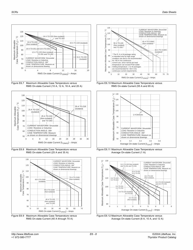
SCRs Data Sheets
http://www.littelfuse.com E6 - 8 ©2004 Littelfuse, Inc.+1 972-580-7777 Thyristor Product Catalog
Figure E6.7 Maximum Allowable Case Temperature versusRMS On-state Current (10 A, 12 A, 16 A, and 20 A)
Figure E6.8 Maximum Allowable Case Temperature versusRMS On-state Current (25 A and 35 A)
Figure E6.9 Maximum Allowable Case Temperature versusRMS On-state Current (40 A through 70 A)
Figure E6.10 Maximum Allowable Case Temperature versusRMS On-state Current (55 A and 65 A)
Figure E6.11 Maximum Allowable Case Temperature versusAverage On-state Current (1 A)
Figure E6.12 Maximum Allowable Case Temperature versusAverage On-state Current (8 A, 10 A, and 12 A)
0 4 8 12 16 2050
60
70
80
90
100
110
120
130
RMS On-state Current [IT(RMS)] – Amps
Max
imum
Allo
wab
leC
ase
Tem
pera
ture
(T
C)
– ˚C
CURRENT WAVEFORM: SinusoidalLOAD: Resistive or InductiveCONDUCTION ANGLE: 180˚CASE TEMPERATURE: Measure asshown on dimensional drawing
10 A TO-220(Non-isolated)
15 A TO-220(Isolated)
20 A TO-220 (Isolated)
16 A TO-220 (Non-isolated)and TO-263
10 A TO-251 and 10 A TO-252
12 A TO-220 (Non-isolated)TO-251 and TO-252
0 4 8 12 16 20 24 28 32 3650
60
70
80
90
100
110
120
130
CURRENT WAVEFORM: SinusoidalLOAD: Resistive or InductiveCONDUCTION ANGLE: 180˚CASE TEMPERATURE: Measureas shown on dimensional drawings
RMS On-state Current [IT(RMS)] – Amps
Max
imum
Allo
wab
leC
ase
Tem
pera
ture
(T
C)
– ˚C
35 A TO-218(Isolated)
25 A TO-220(Non-isolated)
and TO-263
25 A TO-220(Isolated)
0 10 20 30 40 50 60 7050
60
70
80
90
100
110
120
130
RMS On-state Current [IT(RMS)] – Amps
Max
imum
Allo
wab
leC
ase
Tem
pera
ture
(T
C)
– ˚C
65 A TO-218X(Isolated)
55 A TO-218X(Non-isolated)
CURRENT WAVEFORM: SinusoidalLOAD: Resistive or InductiveCONDUCTION ANGLE: 180˚CASE TEMPERATURE: Measure as shown on dimensional drawings
40 A TO-220(Non-isolated)
and TO-263
70 A TO-218X(Non-isolated)
0 10 20 30 4050
60
70
80
90
100
110
120
130
RMS On-state Current [IT(RMS)] – Amps
Max
imum
Allo
wab
le C
ase
Tem
pera
ture
(T
C)
– ˚C
50 60 70 75
CURRENT WAVEFORM: SinusoidalLOAD: Resistive or InductiveCONDUCTION ANGLE: 180˚CASE TEMPERATURE: Measure asshown on dimensional drawings
* The R, K or M package ratingis intended only for high surgecondition use and is not recommendedfor >50 A rms continuouscurrent use, since narrow pin leadtemperature can exceed PCB soldermelting temperature. J or W packagesare recommended for >50 A rmscontinuous current requirements.
65 A TO-218AC(Isolated) *
55 A TO-218AC(Non-isolated) *55 A TO-220
(Non-isolated)and TO-263 *
0 0.2 0.4 0.6 0.850
60
70
80
90
100
110
120
130
CURRENT WAVEFORM: SinusoidalLOAD: Resistive or InductiveCONDUCTION ANGLE: 180˚CASE TEMPERATURE: Measure asshown on dimensional drawings
Average On-state Current [IT(AV)] – Amps
Max
imum
Allo
wab
le C
ase
Tem
pera
ture
(T
C)
– ˚C
1 A Devices
8010 2 3 4 5 6 7 8
90
100
110
120
130
Average On-state Current [IT(AV)] – Amps
Max
imum
Allo
wab
le C
ase
Tem
pera
ture
(T
C)
– ˚C
CURRENT WAVEFORM: SinusoidalLOAD: Resistive or InductiveCONDUCTION ANGLE: 180˚CASE TEMPERATURE: Measure asshown on dimensional drawings
6 A TO-2206 A TO-202
6 A TO-2516 A TO-252
8 A TO-220 (Isolated)8 A TO-202
10 A TO-220 (Isolated)and 10 A TO-202
8 A TO-220(Non-isolated)
12 A TO-220 (Non-isolated)and TO-251 and TO-252
10 A TO-25110 A TO-252
10 A TO-220(Non-isolated)

Data Sheets SCRs
©2004 Littelfuse, Inc. E6 - 9 http://www.littelfuse.comThyristor Product Catalog +1 972-580-7777
Figure E6.13 Maximum Allowable Case Temperature versusAverage On-state Current (10 A through 20 A)
Figure E6.14 Maximum Allowable Case Temperature versusAverage On-state Current (25 A and 35 A)
Figure E6.15 Maximum Allowable Case Temperature versusAverage On-state Current (40 A through 70 A)
Figure E6.16 Maximum Allowable Case Temperature versusAverage On-state Current (55 A and 65 A)
Figure E6.17 Normalized dc Holding Current versus Case Temperature
Figure E6.18 Normalized DC Gate-Trigger Current versusCase Temperature
0 2 4 6 8 10 12 14
50
60
70
80
90
100
110
120
130
Average On-state Current [IT(AV)] – Amps
Max
imum
Allo
wab
le
Cas
e T
empe
ratu
re (
TC
) –
˚C
CURRENT WAVEFORM: SinusoidalLOAD: Resistive or InductiveCONDUCTION ANGLE: 180˚CASE TEMPERATURE: Measuredas shown on dimensional drawings
20 A TO-220(Isolated)
15 A TO-220(Isolated)
10 A TO-220(Non-isolated)
16 A TO-220 (Non-isolated) and TO-263
0 .4 8 12 16 20 24
50
60
70
80
90
100
110
120
130
Average On-state Current [IT(AV)] – Amps
Max
imum
Allo
wab
le C
ase
Tem
pera
ture
(T
C)
– ˚C
CURRENT WAVEFORM: SinusoidalLOAD: Resistive or InductiveCONDUCTION ANGLE: 180˚CASE TEMPERATURE: Measure asshown on dimensional drawings
35 A TO-218 (Isolated)
25A TO-220 (Non-isolated)and TO-263
25A TO-220 (Isolated)
0 10 20 30 40 50
50
60
70
80
90
100
110
120
130
Average On-state Current [IT(AV)] – Amps
Max
imum
Allo
wab
leC
ase
Tem
pera
ture
(T
C)
– ˚C
CURRENT WAVEFORM: SinusoidalLOAD: Resistive or InductiveCONDUCTION ANGLE: 180˚CASE TEMPERATURE: Measure asshown on dimensional drawings
70 A TO-218X(Non-isolated)40 A TO-220
(Non-isolated)and TO-263
55 A TO-218X(Non-isolated)
65 A TO-218X(Isolated)
0 10 20 30 40 50
50
60
70
80
90
100
110
120
130
Average On-state Current [IT(AV)] – Amps
Max
imum
Allo
wab
le
Cas
e T
empe
ratu
re (
TC
) –
˚C
CURRENT WAVEFORM: SinusoidalLOAD: Resistive or InductiveCONDUCTION ANGLE: 180˚CASE TEMPERATURE: Measureas shown on dimensional drawings
55 A TO-218AC (Non-isolated) *
* The R, K, or M packagerating is intended only for highsurge condition use and is notrecommended for >32 A (AV)continuous current use since narrow pin lead temperature can exceed PCBsolder melting temperature. J or Wpackages are recommended for >32 A(AV) continuous current requirements.
55 A TO-220(Non-isolated)and TO-263 *
65 A TO-218AC(Isolated) *
-40 -15 +25 +65 +105 +125
0
.5
1.0
1.5
2.0
Case Temperature (TC) – ˚C
Rat
io o
fI H
I H (
TC
= 2
5 ˚C
)
INITIAL ON-STATE CURRENT =200 mA dc for 1 A to 20 A Devices and 400 mA dc for 25 A to 70 A Devices
-40 -15 +25 +65 +105 +1250
0.5
1.0
1.5
2.0
Case Temperature (TC) – ˚C
Rat
io o
fI G
T
I GT (
TC =
25
˚C)
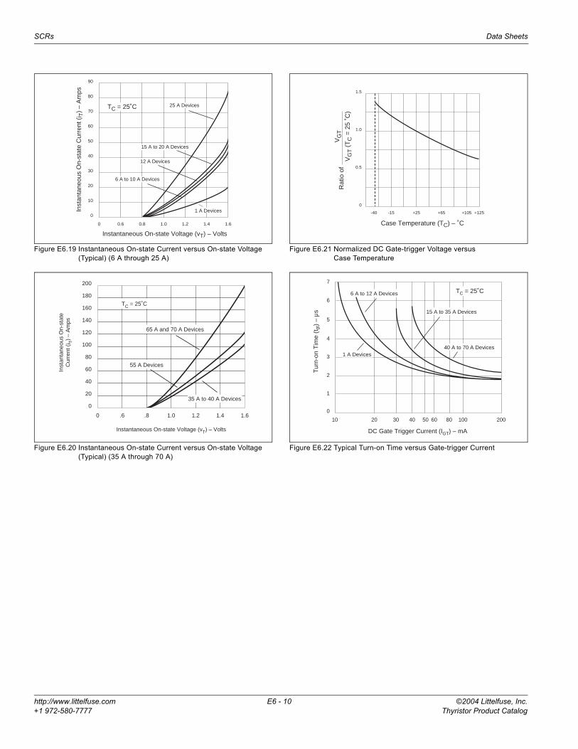
SCRs Data Sheets
http://www.littelfuse.com E6 - 10 ©2004 Littelfuse, Inc.+1 972-580-7777 Thyristor Product Catalog
Figure E6.19 Instantaneous On-state Current versus On-state Voltage (Typical) (6 A through 25 A)
Figure E6.20 Instantaneous On-state Current versus On-state Voltage (Typical) (35 A through 70 A)
Figure E6.21 Normalized DC Gate-trigger Voltage versusCase Temperature
Figure E6.22 Typical Turn-on Time versus Gate-trigger Current
0 0.6 0.8 1.0 1.2 1.4 1.6
0
10
20
30
40
50
60
70
80
90
Instantaneous On-state Voltage (vT) – Volts
Inst
anta
neou
s O
n-st
ate
Cur
rent
(i T
) –
Am
ps
TC = 25˚C
12 A Devices
15 A to 20 A Devices
1 A Devices
6 A to 10 A Devices
25 A Devices
0 .6 .8 1.0 1.2 1.4 1.6
0
20
40
60
80
100
120
140
160
180
200
Instantaneous On-state Voltage (vT) – Volts
Inst
anta
neou
s O
n-st
ate
Cur
rent
(i T
) –
Am
ps
TC = 25˚C
65 A and 70 A Devices
55 A Devices
35 A to 40 A Devices
-40 -15 +25 +65 +105 +125
0
0.5
1.0
1.5
Case Temperature (TC) – ˚C
Rat
io o
fV
GT
VG
T (
TC
= 2
5 ˚C
)
10 20 30 40 50 60 80 100 200
1
2
3
4
5
6
7
0
Tur
n-on
Tim
e (t
gt)
– µs
DC Gate Trigger Current (IGT) – mA
6 A to 12 A Devices
1 A Devices40 A to 70 A Devices
15 A to 35 A Devices
TC = 25˚C

Data Sheets SCRs
©2004 Littelfuse, Inc. E6 - 11 http://www.littelfuse.comThyristor Product Catalog +1 972-580-7777
Figure E6.23 Peak Surge Current versus Surge Current Duration
Figure E6.24 Power Dissipation (Typical) versus RMS On-state Current (1 A)
Figure E6.25 Power Dissipation (Typical) versus RMS On-state Current (6 A through 20 A)
8
1
2
3
456
1000
10
20
30
405060
80100
200
300
400500600
800
1 2 3 54 6 7 8 10 20 30 40 60 80100 200 300400 600 1000
Surge Current Duration – Full Cycles
70 A Devices
65 A TO-218
55 A Devices25 A Devices
35 A Devices
20 A Devices
16 A Devices
15 A Devices
12 A Devices
10 A Devices
1 A Devices
SUPPLY FREQUENCY: 60 Hz SinusoidalLOAD: ResistiveRMS ON-STATE CURRENT: [IT(RMS)]: Max-Rated Value at Specified Case Temperature
Notes:1) Gate control may be lost during and immediately following surge current interval.2) Overload may not be repeated until junction temperature has returned to steady-state rated value.
8 A Devices6 A Devices
Pea
k S
urge
(N
on-r
epet
itive
) O
n-st
ate
Cur
rent
(I T
SM
) –
Am
ps
40 A Devices
0 0.2 0.4 0.6 0.8
0
0.4
0.8
1.0
0.2
RMS On-state Current [IT(RMS)] – Amps
Ave
rage
On-
stat
e P
ower
Dis
sipa
tion
[PD
(AV
)] –
Wat
ts
CURRENT WAVEFORM: Half Sine WaveLOAD: Resistive or InductiveCONDUCTION ANGLE: 180˚
1.0 A Devices
1.0
0.6
0 4 8 12 16
0
RMS On-state Current [IT(RMS)] – Amps
Ave
rage
On-
stat
eP
ower
Dis
sipa
tion
[PD
(AV
)] –
Wat
ts
CURRENT WAVEFORM: Half Sine WaveLOAD: Resistive or InductiveCONDUCTION ANGLE: 180˚
2 6 10 14 18
2
4
6
8
10
12
14
16
18
20
15 A to 20 A Devices
12 A Devices
6 A to 10 A Devices
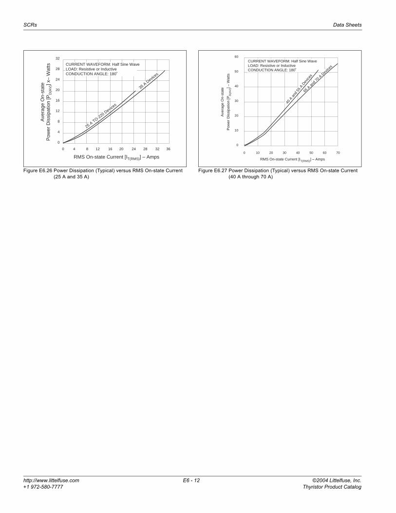
SCRs Data Sheets
http://www.littelfuse.com E6 - 12 ©2004 Littelfuse, Inc.+1 972-580-7777 Thyristor Product Catalog
Figure E6.26 Power Dissipation (Typical) versus RMS On-state Current(25 A and 35 A)
Figure E6.27 Power Dissipation (Typical) versus RMS On-state Current (40 A through 70 A)
0 8 16 24 32
0
RMS On-state Current [IT(RMS)] – Amps
Ave
rage
On-
stat
eP
ower
Dis
sipa
tion
[PD
(AV
)] x–
Wat
ts
4 12 20 28 36
4
8
12
16
20
24
28
32
25 A TO-220 Devic
es
35 A D
evices
CURRENT WAVEFORM: Half Sine WaveLOAD: Resistive or InductiveCONDUCTION ANGLE: 180˚
RMS On-state Current [IT(RMS)] – Amps
Ave
rage
On-
stat
e
Pow
er D
issi
patio
n [P
D(A
V)]
– W
atts
0 10 20 30 40 50 60 70
0
10
20
30
40
50
60
65 A
and 7
0 A D
evice
s
CURRENT WAVEFORM: Half Sine WaveLOAD: Resistive or InductiveCONDUCTION ANGLE: 180˚
40 A
and
55
A Dev
ices

U.L
. REC
OG
NIZ
ED
File #E71639
TO-220Isolated
A C
©2004 Littelfuse, Inc. E7 - 1 http://www.littelfuse.comThyristor Product Catalog + 1 972-580-7777
Rectifiers(15 A to 25 A)
E7General DescriptionTeccor manufactures 15 A rms to 25 A rms rectifiers with volt-ages rated from 200 V to 1000 V. Due to the electrically-isolated TO-220 package, these rectifiers may be used in common anode or common cathode circuits using only one part type, thereby simplifying stock requirements.Teccor's silicon rectifiers feature glass-passivated junctions to ensure long term reliability and stability. In addition, glass offers a rugged, reliable barrier against junction contamination.
Features• Electrically-isolated packages• High voltage capabilities — 200 V to 1000 V• High surge capabilities — up to 350 A• Glass-passivated junctions
E7

http://www.littelfuse.com E7 - 2 ©2004 Littelfuse, Inc.+ 1 972-580-7777 Thyristor Product Catalog
Rectifiers Data Sheets
Test ConditionsI2t — RMS surge (non-repetitive) forward current for 8.3 ms for fusingIF(AV) — Average forward currentIF(RMS) — RMS forward currentIFSM — Peak one-cycle surge currentIRM — Peak reverse currentRθJC — Thermal resistance (steady state) junction to caseVFM — Peak forward voltage at rated average forward currentVR — DC blocking voltageVRRM — Peak repetitive reverse voltage
General Notes• Operating temperature range (TJ) is -40 °C to +125 °C.• Storage temperature range (TS) is -40 °C to +125 °C.• Lead solder temperature is a maximum of 230 °C for 10 seconds
maximum at a minimum of 1/16" (1.59 mm) from case.• The case temperature (TC) is measured as shown on dimensional
outline drawings in the “Package Dimensions” section of this catalog.
• Teccor's electrically-isolated TO-220 devices withstand a high potential test of 2500 V ac rms from leads to mounting tab over the operating temperature range.
• Typical Reverse Recovery Time (trr) is 4 µs. (Test conditions =0.9 A forward current and 1.5 A reverse current.)
Electrical Specification Notes(1) See Figure E7.3 for current rating at specified case temperature.(2) For more than one full cycle rating, see Figure E7.4.(3) TC = TJ for test conditions(4) See package outlines for lead form configurations. When ordering
special lead forming, add type number as suffix to part number.
Electrical Isolation
* UL Recognized File #E71639** For 4000 V isolation, use “V” suffix in the part number.
Type
Part NumberVRRM VR IF(AV) IF(RMS) IFSM IRM VFM I2t RθJCIsolated
TO-220Volts Volts
(1)
Amps Amps
(2)
Amps
(3)
mA Volts
Amps2Sec °C/W60/50 HzTC =25 °C
TC =100 °C
TC =125 °C TC=25 °C
See “Package Dimensions” section for variations. (4) MIN MIN MAX MAX MAX MAX TYP
15 A
D2015L 200 200 9.5 15 225/188 0.1 0.5 1 1.6 210 2.85D4015L 400 400 9.5 15 225/188 0.1 0.5 1 1.6 210 2.85D6015L 600 600 9.5 15 225/188 0.1 0.5 1 1.6 210 2.85D8015L 800 800 9.5 15 225/188 0.1 0.5 1 1.6 210 2.85DK015L 1000 1000 9.5 15 225/188 0.1 3 1.6 210 2.85
20 A
D2020L 200 200 12.7 20 300/255 0.1 0.5 1 1.6 374 2.5D4020L 400 400 12.7 20 300/255 0.1 0.5 1 1.6 374 2.5D6020L 600 600 12.7 20 300/255 0.1 0.5 1 1.6 374 2.5D8020L 800 800 12.7 20 300/255 0.1 0.5 1 1.6 374 2.5DK020L 1000 1000 12.7 20 300/255 0.1 3 1.6 374 2.5
25 A
D2025L 200 200 15.9 25 350/300 0.1 0.5 1 1.6 508 2.7D4025L 400 400 15.9 25 350/300 0.1 0.5 1 1.6 508 2.7D6025L 600 600 15.9 25 350/300 0.1 0.5 1 1.6 508 2.7D8025L 800 800 15.9 25 350/300 0.1 0.5 1 1.6 508 2.7DK025L 1000 1000 15.9 25 350/300 0.1 3 1.6 508 2.7
CA
NotUsed
Electrical Isolationfrom Leads to Mounting Tab *
V AC RMSTO-220Isolated
2500 Standard
4000 Optional **

©2004 Littelfuse, Inc. E7 - 3 http://www.littelfuse.comThyristor Product Catalog +1 972-580-7777
Data Sheets Rectifiers
Figure E7.1 Instantaneous Forward Current versus Forward Voltage (Typical)
Figure E7.2 Forward Power Dissipation (Typical)
Figure E7.3 Maximum Allowable Case Temperature versusAverage Forward Current
Figure E7.4 Peak Surge Forward Current versus Surge Current Duration
0 0.6 0.8 1.0 1.2 1.4 1.6 1.8
0
20
40
60
80
100
120
140
Instantaneous Forward Voltage (vF) – Volts
Inst
anta
neou
s F
orw
ard
Cur
rent
(i F
) –
Am
ps
15 A Devices
TC = 25˚C
20 A Devices
25 A Devices
16120 2 4 6 8 10 12 14
0
4
8
12
16
20
SINGLE PULSE RECTIFICATION60 Hz SINE WAVE
20 A Devices
15 A Devices
25 A Devices
Average Forward Current [IF(AV)] – Amps
Ave
rage
For
war
dP
ower
Dis
sipa
tion
[PF
(AV
)] –
Wat
ts
0 2 4 6 8 10 12 14
0
70
75
80
85
90
95
100
105
110
115
120
125
20 A Devices
15 A Devices
Average Forward Current [IF (AV)] – Amps
Max
imum
Allo
wab
le C
ase
Tem
pera
ture
(TC) –
˚C
SUPPLY FREQUENCY: 60 Hz Sine WaveLOAD: Resistive or InductiveCASE TEMPERATURE:Measured As Shown on Dimensional Drawing
16
25 A Devices
10
20
3040
6080
100
200
300400
600800
1000
1 2 4 6 10 20 40 60 100 200 400 600 1000
Surge Current Duration – Cycles
SUPPLY FREQUENCY: 60 Hz SinewaveLOAD: Resistive or InductiveRMS ON-STATE CURRENT: [IF(RMS)]Maximium Rated Value at SpecifiedCase Temperature
15 A Devices
20 A Devices25 A Devices
Pea
k S
urge
(N
on-r
epet
itive
)F
orw
ard
Cur
rent
(I F
SM
) –
Am
ps

Notes

2004 Littelfuse, Inc. E8 - 1 http://www.littelfuse.comThyristor Product Catalog +1 972-580-7777
DiacHT and ST Series
E8General DescriptionTeccor’s HT and ST Series of bilateral trigger diacs offer a range of voltage characteristics from 27 V to 70 V.A diac semiconductor is a full-wave or bidirectional thyristor. It is triggered from a blocking state to a conduction state for either polarity of applied voltage whenever the amplitude of applied voltage exceeds the breakover voltage rating of the diac.The Teccor line of diacs features glass-passivated junctions to ensure long-term reliability and parameter stability. Teccor’s glass offers a rugged, reliable barrier against junction contamination.The diac specifications listed in this data sheet are for standard products. Special parameter selections such as close tolerance voltage symmetry are available. Consult the factory for more information about custom design applications.
Features• Bilateral triggering device• Glass-passivated junctions• Wide voltage range selections
ST Series• Epoxy SMT package• High-temperature, solder-bonded die attachment
HT Series• DO-35 trigger package• Pre-tinned leads
E8
DO-214
DO-35

Diac Data Sheets
http://www.littelfuse.com E8 - 2 2004 Littelfuse, Inc.+1 972-580-7777 Thyristor Product Catalog
General Notes• Lead solder temperature is +230 °C for 10-second maximum;
≥1/16" (1.59 mm) from case.• See “Package Dimensions” section of this catalog.
Electrical Specification Notes(1) Breakover voltage symmetry as close as 1 V is available from the
factory on these products.(2) See Figure E8.4 and Figure E8.5 for test circuit and waveforms.(3) Typical switching time is 900 nano-seconds measured at IPK
(Figure E8.4) across a 20 Ω resistor (Figure E8.5). Switching time is defined as rise time of IPK between the 10% to 90% points.
(4) See V-I Characteristics.
Bilateral Trigger DIAC Specifications• Maximum Ratings, Absolute-Maximum Values
– Maximum Trigger Firing Capacitance: 0.1 µF– Device dissipation (at TA = -40 °C to +40 °C):
250 mW for DO-35 and 300 mW for DO-214– Derate above +40 °C:
3.6 mW/°C for DO-35 and 3 mW/°C for DO-214• Temperature Ranges
Storage: -40 °C to +125 °COperating (Junction): -40 °C to +125 °C
V-I Characteristics
* Mounted on 1 cm2 copper foil surface; two-ounce copper foil
Electrical Characteristics TC = 25°CPart No. VBO ∆VBO VBB IBO ITRM
DO-35 DO-214
Breakover Voltage (Forward and
Reverse)
Volts
Breakover Voltage Symmetry
∆VBO =[ | +VBO | - | - VBO | ]
Volts
DynamicBreakback
Voltage(3)
| ∆V± |
Volts
Peak BreakoverCurrent
atBreakover
Voltage
µAmps
Peak PulseCurrent
for 10 µs 120 PPS
TA ≤40 °C
AmpsMIN MAX MAX MIN MAX MAX
HT-32 ST-32 27 37 3 (1) 10 (2) 25 2HT-32A / HT-5761 28 36 2 (1) 7 at 10 mA (4) 25 2
HT-32B / HT-5761A ST-32B 30 34 2 (1) 7 at 10 mA (4) 25 2HT-34B ST-34B 32 36 2 (1) 10 (2) 25 2HT-35 ST-35 30 40 3 (1) 10 (2) 25 2
HT-36A / HT-5762 ST-36A 32 40 2 (1) 7 at 10 mA (4) 25 2HT-36B ST-36B 34 38 2 (1) 10 (2) 25 2HT-40 ST-40 35 45 3 (1) 10 (2) 25 2HT-60 56 70 4 20 (2) 25 1.5
HT and ST Series Thermal ResistanceJunction to Lead - RθJL: °C/W
Junction to Ambient [RθJA]: °C/W(based on maximum lead temperature of
90 °C for DO-214 and 85 °C for DO-35 devices)Y Package
DO-35
S Package
DO-214
100 [278] °C/W 65 °C/W *
10 mA
BreakoverCurrent
IBO
-VBO
Voltage
Current
BreakoverVoltage
VBO
+VBO
V
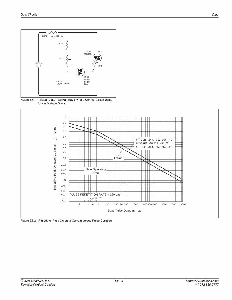
Data Sheets Diac
2004 Littelfuse, Inc. E8 - 3 http://www.littelfuse.comThyristor Product Catalog +1 972-580-7777
Figure E8.1 Typical Diac/Triac Full-wave Phase Control Circuit Using Lower Voltage Diacs.
Figure E8.2 Repetitive Peak On-state Current versus Pulse Duration
120 V ac60 Hz
LOAD — Up to 1500 W
3.3 k
200 k
0.1 µF100 V
HT-35BilateralTrigger
Diac
TriacQ2015L5
MT2
MT1G
1 2 4 6 200 4006001000 2000 4000 10000
.001
.002
.003
.005
0.1
0.2
0.3
3.0
0.5
5.0
.01
0.02
0.03
0.05
1.0
10
2.0
Rep
etiti
ve P
eak
On-
stat
e C
urre
nt (
I TR
M)
– A
mps
Base Pulse Duration – µs
Safe OperatingArea
10 20 40 60 100
PULSE REPETITION RATE = 120 ppsTA = 40 ˚C
HT-60
HT-32x, -34x, -35, -36x, -40HT-5761, -5761A, -5762ST-32x, -34x, -35, -36x, -40
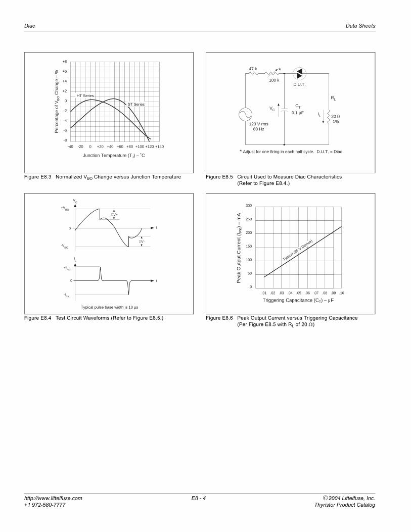
Diac Data Sheets
http://www.littelfuse.com E8 - 4 2004 Littelfuse, Inc.+1 972-580-7777 Thyristor Product Catalog
Figure E8.3 Normalized VBO Change versus Junction Temperature
Figure E8.4 Test Circuit Waveforms (Refer to Figure E8.5.)
Figure E8.5 Circuit Used to Measure Diac Characteristics(Refer to Figure E8.4.)
Figure E8.6 Peak Output Current versus Triggering Capacitance(Per Figure E8.5 with RL of 20 Ω)
-8
-6
-4
-2
0
+2
+4
+6
+8
-40 -20 0 +20 +40 +60 +80 +100 +120 +140
Junction Temperature (TJ) – ˚C
Per
cent
age
of V
BO C
hang
e –
%
ST Series
HT Series
∆V+
∆V-
VC
0
-VBO
IL
+IPK
0 t
-IPK
t
+VBO
Typical pulse base width is 10 µs
120 V rms60 Hz
47 k
D.U.T.
RL
20 Ω1%
VC
100 k
*
CT
IL0.1 µF
* Adjust for one firing in each half cycle. D.U.T. = Diac
Triggering Capacitance (CT) – µF
Peak
Outp
ut C
urr
ent (I
PK)
– m
A
.01 .02 .03 .04 .05 .06 .07 .08 .09
0
50
100
150
200
250
300
Typica
l (35 V Devic
e)
.10
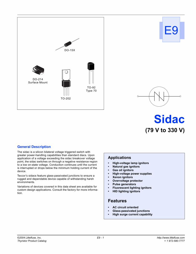
©2004 Littelfuse, Inc. E9 - 1 http://www.littelfuse.comThyristor Product Catalog + 1 972-580-7777
Sidac(79 V to 330 V)
E9General DescriptionThe sidac is a silicon bilateral voltage triggered switch with greater power-handling capabilities than standard diacs. Upon application of a voltage exceeding the sidac breakover voltage point, the sidac switches on through a negative resistance region to a low on-state voltage. Conduction continues until the current is interrupted or drops below the minimum holding current of the device.Teccor’s sidacs feature glass-passivated junctions to ensure a rugged and dependable device capable of withstanding harsh environments.Variations of devices covered in this data sheet are available for custom design applications. Consult the factory for more informa-tion.
Applications• High-voltage lamp ignitors• Natural gas ignitors• Gas oil ignitors• High-voltage power supplies• Xenon ignitors• Overvoltage protector• Pulse generators• Fluorescent lighting ignitors• HID lighting ignitors
Features• AC circuit oriented• Glass-passivated junctions• High surge current capability
E9
TO-92Type 70
DO-214Surface Mount
TO-202
DO-15X
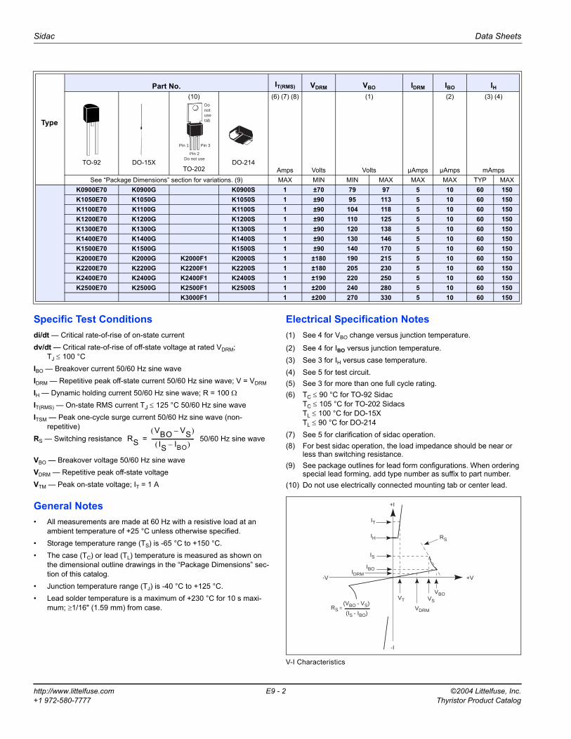
http://www.littelfuse.com E9 - 2 ©2004 Littelfuse, Inc.+1 972-580-7777 Thyristor Product Catalog
Sidac Data Sheets
Specific Test Conditionsdi/dt — Critical rate-of-rise of on-state currentdv/dt — Critical rate-of-rise of off-state voltage at rated VDRM;
TJ ≤ 100 °CIBO — Breakover current 50/60 Hz sine waveIDRM — Repetitive peak off-state current 50/60 Hz sine wave; V = VDRM
IH — Dynamic holding current 50/60 Hz sine wave; R = 100 Ω
IT(RMS) — On-state RMS current TJ ≤ 125 °C 50/60 Hz sine waveITSM — Peak one-cycle surge current 50/60 Hz sine wave (non-
repetitive)RS — Switching resistance 50/60 Hz sine wave
VBO — Breakover voltage 50/60 Hz sine waveVDRM — Repetitive peak off-state voltageVTM — Peak on-state voltage; IT = 1 A
General Notes• All measurements are made at 60 Hz with a resistive load at an
ambient temperature of +25 °C unless otherwise specified.• Storage temperature range (TS) is -65 °C to +150 °C.• The case (TC) or lead (TL) temperature is measured as shown on
the dimensional outline drawings in the “Package Dimensions” sec-tion of this catalog.
• Junction temperature range (TJ) is -40 °C to +125 °C.• Lead solder temperature is a maximum of +230 °C for 10 s maxi-
mum; ≥1/16" (1.59 mm) from case.
Electrical Specification Notes(1) See 4 for VBO change versus junction temperature.
(2) See 4 for IBO versus junction temperature.(3) See 3 for IH versus case temperature.(4) See 5 for test circuit.(5) See 3 for more than one full cycle rating.(6) TC ≤ 90 °C for TO-92 Sidac
TC ≤ 105 °C for TO-202 SidacsTL ≤ 100 °C for DO-15XTL ≤ 90 °C for DO-214
(7) See 5 for clarification of sidac operation.(8) For best sidac operation, the load impedance should be near or
less than switching resistance.(9) See package outlines for lead form configurations. When ordering
special lead forming, add type number as suffix to part number.(10) Do not use electrically connected mounting tab or center lead.
V-I Characteristics
Type
Part No. IT(RMS) VDRM VBO IDRM IBO IH
TO-92 DO-15X
(10)
TO-202DO-214
(6) (7) (8)
Amps Volts
(1)
Volts µAmps
(2)
µAmps
(3) (4)
mAmpsSee “Package Dimensions” section for variations. (9) MAX MIN MIN MAX MAX MAX TYP MAX
K0900E70 K0900G K0900S 1 ±70 79 97 5 10 60 150K1050E70 K1050G K1050S 1 ±90 95 113 5 10 60 150K1100E70 K1100G K1100S 1 ±90 104 118 5 10 60 150K1200E70 K1200G K1200S 1 ±90 110 125 5 10 60 150K1300E70 K1300G K1300S 1 ±90 120 138 5 10 60 150K1400E70 K1400G K1400S 1 ±90 130 146 5 10 60 150K1500E70 K1500G K1500S 1 ±90 140 170 5 10 60 150K2000E70 K2000G K2000F1 K2000S 1 ±180 190 215 5 10 60 150K2200E70 K2200G K2200F1 K2200S 1 ±180 205 230 5 10 60 150K2400E70 K2400G K2400F1 K2400S 1 ±190 220 250 5 10 60 150K2500E70 K2500G K2500F1 K2500S 1 ±200 240 280 5 10 60 150
K3000F1 1 ±200 270 330 5 10 60 150
Pin 1
Pin 2Do not use
Pin 3
Donot usetab
RSVBO VS–( )
IS IBO–( )--------------------------------=
-V
+I
VDRM
+V
VS
IS
IH RS
IDRM
IBO
VBOVT
IT
(IS - IBO)
(VBO - VS)RS =
-I
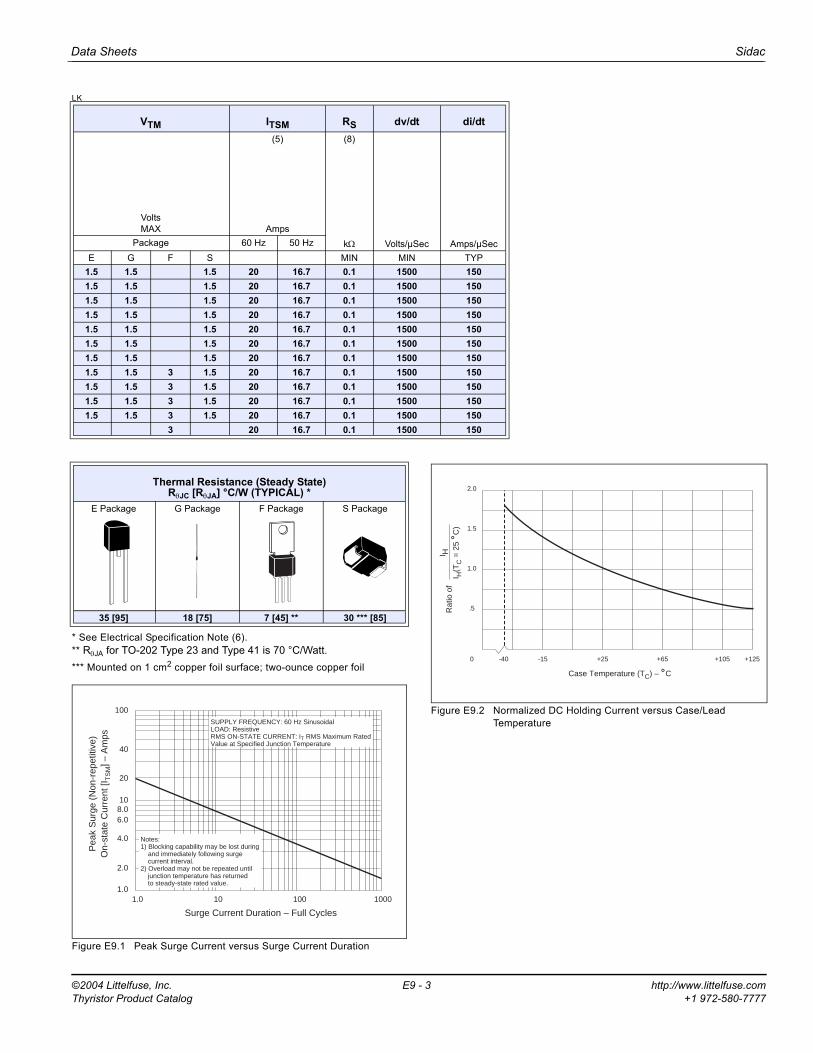
©2004 Littelfuse, Inc. E9 - 3 http://www.littelfuse.comThyristor Product Catalog +1 972-580-7777
Data Sheets Sidac
LK
* See Electrical Specification Note (6).** RθJA for TO-202 Type 23 and Type 41 is 70 °C/Watt.*** Mounted on 1 cm2 copper foil surface; two-ounce copper foil
Figure E9.1 Peak Surge Current versus Surge Current Duration
Figure E9.2 Normalized DC Holding Current versus Case/Lead Temperature
VTM ITSM RS dv/dt di/dt
VoltsMAX
(5)
Amps
(8)
kΩ Volts/µSec Amps/µSecPackage 60 Hz 50 HzE G F S MIN MIN TYP
1.5 1.5 1.5 20 16.7 0.1 1500 1501.5 1.5 1.5 20 16.7 0.1 1500 1501.5 1.5 1.5 20 16.7 0.1 1500 1501.5 1.5 1.5 20 16.7 0.1 1500 1501.5 1.5 1.5 20 16.7 0.1 1500 1501.5 1.5 1.5 20 16.7 0.1 1500 1501.5 1.5 1.5 20 16.7 0.1 1500 1501.5 1.5 3 1.5 20 16.7 0.1 1500 1501.5 1.5 3 1.5 20 16.7 0.1 1500 1501.5 1.5 3 1.5 20 16.7 0.1 1500 1501.5 1.5 3 1.5 20 16.7 0.1 1500 150
3 20 16.7 0.1 1500 150
Thermal Resistance (Steady State)RθJC [RθJA] °C/W (TYPICAL) *
E Package G Package F Package S Package
35 [95] 18 [75] 7 [45] ** 30 *** [85]
1.0 10 100 10001.0
2.0
4.0
6.08.010
20
40
SUPPLY FREQUENCY: 60 Hz SinusoidalLOAD: ResistiveRMS ON-STATE CURRENT: IT RMS Maximum Rated Value at Specified Junction Temperature
Notes:1) Blocking capability may be lost during and immediately following surge current interval.2) Overload may not be repeated until junction temperature has returned to steady-state rated value.
Surge Current Duration – Full Cycles
Pea
k S
urge
(N
on-r
epet
itive
)O
n-st
ate
Cur
rent
[IT
SM
] – A
mps
100
0
.5
1.0
2.0
1.5
-15-40 +25 +65 +105 +125
Case Temperature (TC) – ˚C
I HI H
(TC
= 2
5 ˚C
)R
atio
of
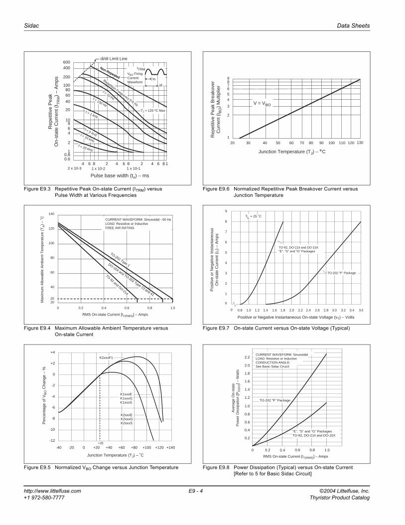
http://www.littelfuse.com E9 - 4 ©2004 Littelfuse, Inc.+1 972-580-7777 Thyristor Product Catalog
Sidac Data Sheets
Figure E9.3 Repetitive Peak On-state Current (ITRM) versusPulse Width at Various Frequencies
Figure E9.4 Maximum Allowable Ambient Temperature versusOn-state Current
Figure E9.5 Normalized VBO Change versus Junction Temperature
Figure E9.6 Normalized Repetitive Peak Breakover Current versus Junction Temperature
Figure E9.7 On-state Current versus On-state Voltage (Typical)
Figure E9.8 Power Dissipation (Typical) versus On-state Current[Refer to 5 for Basic Sidac Circuit]
di/dt Limit Line
0.60.8
4
2
468
10
20
40
6080
100
200
400600
2 x 10-36 8
1 x 10-22 4 6 8
1 x 10-12 4 6 8 1
1
Pulse base width (to) – ms
Rep
etiti
ve P
eak
On-
stat
e C
urre
nt (
I TR
M)
– A
mps
VBO FiringCurrentWaveform
Non-RepeatedRepetition Frequency f=5 Hz
f = 10 Hzf = 100 Hz
f = 1 kHz
f = 5 kHzf = 10 kHz
f = 20 kHz
TJ = 125 ºC Max
to
ITRM
l/f
Non-Repeated
0 0.2 0.4 0.6 0.8 1.0
20
40
60
80
100
120
140
25
RMS On-state Current [IT(RMS)] – Amps
Max
imum
Allo
wab
le A
mbi
ent T
empe
ratu
re (
TA)
– ˚C CURRENT WAVEFORM: Sinusoidal - 60 Hz
LOAD: Resistive or InductiveFREE AIR RATING
TO-92 and DO-214
DO-15X and TO-202 Type 23 and 41
TO-202 Type 1
-12
-20 0 +20 +40 +60 +80 +100 +120
-10
-8
-6
-4
-2
0
+2
+4
-40+25
Junction Temperature (TJ) – ˚C
Per
cent
age
of V
BO
Cha
nge
– %
+140
K2xxxF1
K1xxxEK1xxxGK1xxxS
K2xxxEK2xxxGK2xxxS
20 30 40 50 60 8070 90 100 110 1201
2
3
456789
Junction Temperature (TJ) – ˚C
Rep
etiti
ve P
eak
Bre
akov
erC
urre
nt (
I BO
) M
ultip
lier
V = VBO
130
0 0.8 1.21.0 1.4 1.6 1.8 2.0 2.2 2.4 2.6 2.8 3.0 3.2 3.4 3.6
0
1
2
3
4
5
6
7
8
9
Positive or Negative Instantaneous On-state Voltage (vT) – Volts
Pos
itive
or
Neg
ativ
e In
stan
tane
ous
On-
stat
e C
urre
nt (
i T)
– A
mps
TL = 25 ˚C
TO-92, DO-214 and DO-15X"E", "S" and "G" Packages
TO-202 "F" Package
0.2 0.4 0.6 0.8 1.00
0.4
0.8
1.2
1.6
0.2
0.6
1.0
1.4
1.8
2.0
2.2
RMS On-state Current [IT(RMS)] – Amps
Ave
rage
On-
stat
eP
ower
Dis
sipa
tion
[PD
(AV
)] –
Wat
ts
"E", "S" and "G" PackagesTO-92, DO-214 and DO-15X
TO-202 "F" Package
CURRENT WAVEFORM: SinusoidalLOAD: Resistive or InductiveCONDUCTION ANGLE:See Basic Sidac Cirucit
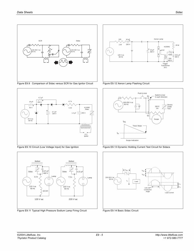
©2004 Littelfuse, Inc. E9 - 5 http://www.littelfuse.comThyristor Product Catalog +1 972-580-7777
Data Sheets Sidac
Figure E9.9 Comparison of Sidac versus SCR for Gas Ignitor Circuit
Figure E9.10 Circuit (Low Voltage Input) for Gas Ignition
Figure E9.11 Typical High Pressure Sodium Lamp Firing Circuit
Figure E9.12 Xenon Lamp Flashing Circuit
Figure E9.13 Dynamic Holding Current Test Circuit for Sidacs
Figure E9.14 Basic Sidac Circuit
100-250 V ac60 Hz
100-250 V ac60 Hz
SCR Sidac
4.7 µF
100 V10 µF
50 V
24 V ac60 Hz
4.7 µF100 V
½ W K1200ESidac
200 V
H.V.Ignitor
1.2 µF
4.7 k- +
- +
+-
Sidac
120 V ac60 Hz
16 mH
3.3 k
0.47 µF400 V
Ballast
Sidac
220 V ac60 Hz
7.5 k
0.22 µF
Ballast
Lamp
120 V ac 220 V ac
Lamp
- +
+-
Xenon Lamp
K2200G
10 µF
2 W
120 V ac60 Hz
10 µF450 V
4 kV
0.01 µF400 V
20 M
Sidac
200-400 V
100
250 V
Trigger Transformer
20:1
100-250 V ac 60 Hz
Scope
Push to test
S1Switch to testin each direction
100 Ω1%
DeviceUnderTest
S1
Scope Indication
Trace Stops
IH
IPK
Load
100-250 V ac60 Hz
IH
VBO
120-145˚ConductionAngle
IH
IH
Load Current
VBO
VBO

http://www.littelfuse.com E9 - 6 ©2004 Littelfuse, Inc.+1 972-580-7777 Thyristor Product Catalog
Sidac Data Sheets
Figure E9.15 Relaxation Oscillator Using a Sidac
Figure E9.16 Sidac Added to Protect Transistor for Typical Transistor Inductive Load Switching Requirements
VDC(IN) ≥ VB0 VC
IL RL
R
SIDAC
(a) Circuit
Rmax ≤VIN - VBO
IBO
Rmin ≥VIN - VTMIH (MIN)
(b) WaveformsVBO
VC
IL
t
t
C
VCE Monitor
100 mH
IC Monitor+
-
RS = 0.1 Ω
Test Circuit
VBB1 =10 V
+
-
VBB2 =0
RBB2 =100 Ω
RBB1 =150 Ω
2N6127(or equivalent)
50 Ω
50 Ω
Input
(See Note B)
TIP-47
VCC = 20 V
Voltage and Current Waveforms
InputVoltage
0 V
5 V
0.63 A
0
Sidac VBO
10 V
VCE(sat)
tw ≈ 3 ms(See Note A)
CollectorCurrent
CollectorVoltage
100 ms
tw
Note A: Input pulse width is increased until ICM = 0.63 A.
Note B: Sidac (or Diac or series of Diacs) chosen so that VBO is just below VCEO rating of transistor to be protected. The Sidac (or Diac) eliminates a reverse breakdown of the transistor in inductive switching circuits where otherwise the transistor could be destroyed.