Embed Size (px)
Citation preview

PowerPlay Early Power EstimatorUser GuideUG-010702017.02.21
SubscribeSend Feedback
Contents
1 PowerPlay Early Power Estimator Overview.................................................................... 31.1 Release Information................................................................................................31.2 Power Model Status for Supported Device Families...................................................... 4
2 Setting Up the PowerPlay Early Power Estimator.............................................................52.1 System Requirements............................................................................................. 52.2 Download and Install the PowerPlay Early Power Estimator...........................................5
2.2.1 Changing the Macro Security Level in Microsoft Excel 2003...............................52.2.2 Changing the Macro Security Level in Microsoft Excel 2007...............................52.2.3 Changing the Macro Security Level in Microsoft Excel 2010...............................6
2.3 Estimating Power Consumption.................................................................................62.3.1 Estimating Power Consumption Before Starting the FPGA Design.......................62.3.2 Estimating Power Consumption While Creating the FPGA Design........................72.3.3 Estimating Power Consumption After Completing the FPGA Design.................... 9
3 PowerPlay Early Power Estimator Worksheets...............................................................103.1 Main Worksheet....................................................................................................10
3.1.1 Input Parameter....................................................................................... 113.1.2 Thermal Power......................................................................................... 133.1.3 Power Tree Design.................................................................................... 153.1.4 Thermal Analysis...................................................................................... 16
3.2 Logic Worksheet................................................................................................... 203.3 RAM Worksheet.................................................................................................... 223.4 DSP Worksheet.....................................................................................................253.5 I/O Worksheet......................................................................................................263.6 PLL Worksheet......................................................................................................303.7 Clock Worksheet...................................................................................................313.8 HSDI Worksheet................................................................................................... 323.9 XCVR Worksheet...................................................................................................343.10 HMC Worksheet.................................................................................................. 383.11 IP Worksheet......................................................................................................393.12 HPS Worksheet................................................................................................... 403.13 Report Worksheet............................................................................................... 41
3.13.1 Static Power and Dynamic Current per Voltage Rail......................................413.13.2 Power Up Current....................................................................................413.13.3 Power Breakout for Multiple Voltage Supplies.............................................. 413.13.4 Power Regulator Settings......................................................................... 42
3.14 Enpirion Worksheet............................................................................................. 42
4 Factors Affecting the PowerPlay Early Power Estimator Spreadsheet Accuracy............. 444.1 Toggle Rate..........................................................................................................444.2 Airflow................................................................................................................ 454.3 Temperature........................................................................................................ 464.4 Heat Sink............................................................................................................ 47
A Additional Information for PowerPlay Early Power Estimator User Guide ..................... 48A.1 Document Revision History for PowerPlay Early Power Estimator User Guide ................ 48
Contents
PowerPlay Early Power Estimator User Guide2
1 PowerPlay Early Power Estimator OverviewThis user guide describes the PowerPlay Early Power Estimator (EPE) support forArria® II, Arria V, Cyclone® III, Cyclone IV, Cyclone V, Stratix® III, Stratix IV, StratixV, and MAX® 10 device families. This user guide provides guidelines to use thePowerPlay EPE at any stage of the FPGA design and provides details about thermalanalysis and the factors that contribute to FPGA power consumption. You can calculatethe FPGA power with the Microsoft Excel-based PowerPlay EPE spreadsheet. For moreaccurate power estimation, use the PowerPlay Power Analyzer in the Quartus® II orQuartus Prime software.
Intel recommends switching from the PowerPlay EPE spreadsheet to the PowerPlayPower Analyzer in the Quartus II or Quartus Prime software once the design isavailable. The PowerPlay Power Analyzer has access to the implemented design detailsto produce more accurate results.
Intel recommends using these calculations as an estimation of power, not as aspecification. You must verify the actual power during device operation as theinformation is sensitive to the actual device design and the environmental operatingconditions.
The features of the PowerPlay EPE spreadsheet include:
• Estimating the power consumption of your design before creating the design orduring the design process
• Importing device resource information from the Quartus II or Quartus Primesoftware into the PowerPlay EPE spreadsheet with the use of the Quartus II orQuartus Prime-generated PowerPlay EPE file
• Performing preliminary thermal analysis of your design
Related Links
• PowerPlay Power Analysis chapter in volume 3 of the Quartus II Handbook
• PowerPlay Early Power Estimator for Intel CPLDs User Guide
1.1 Release Information
Release information describes the supported device families and version of thePowerPlay EPE spreadsheet, which is documented in this user guide.
You should always use the latest version of the PowerPlay EPE spreadsheet.
Related Links
PowerPlay Early Power Estimators (EPE) and Power Analyzer
1 PowerPlay Early Power Estimator Overview
Intel Corporation. All rights reserved. Intel, the Intel logo, Altera, Arria, Cyclone, Enpirion, MAX, Nios, Quartusand Stratix words and logos are trademarks of Intel Corporation or its subsidiaries in the U.S. and/or othercountries. Intel warrants performance of its FPGA and semiconductor products to current specifications inaccordance with Intel's standard warranty, but reserves the right to make changes to any products and servicesat any time without notice. Intel assumes no responsibility or liability arising out of the application or use of anyinformation, product, or service described herein except as expressly agreed to in writing by Intel. Intelcustomers are advised to obtain the latest version of device specifications before relying on any publishedinformation and before placing orders for products or services.*Other names and brands may be claimed as the property of others.
ISO9001:2008Registered

1.2 Power Model Status for Supported Device Families
The power models in the PowerPlay EPE spreadsheet are either in preliminary or finalstatus. Preliminary power models are subject to change. Preliminary power models arecreated based on simulation results, process data, and other known parameters. Thefinal power models are created based on a complete correlation to the productiondevice. If the power models are final, there are no further changes to the powermodels. The power model status for the device will be shown in the Main worksheet ofthe PowerPlay EPE spreadsheet.
For the majority of the designs, the PowerPlay Power Analyzer and the PowerPlay EPEspreadsheet have the following accuracy after the power models are final:
• PowerPlay Power Analyzer: ± 20% from silicon, assuming that PowerPlay PowerAnalyzer uses the Value Change Dump File (.vcd) generated toggle rates
• PowerPlay EPE spreadsheet: ± 30% from silicon, assuming PowerPlay EPE dataimported from PowerPlay Power Analyzer results using .vcd generated togglerates
The toggle rates are derived using the PowerPlay Power Analyzer with a .vcd filegenerated from a gate level simulation representative of the system operation.
Related Links
PowerPlay Early Power Estimators (EPE) and Power Analyzer
1 PowerPlay Early Power Estimator Overview
PowerPlay Early Power Estimator User Guide4
2 Setting Up the PowerPlay Early Power Estimator
2.1 System Requirements
The PowerPlay EPE spreadsheet requires the following software:
• Windows operating system that the Quartus II software supports
• Microsoft Excel 2003, Microsoft Excel 2007, or Microsoft Excel 2010
• Quartus II software version 9.1 or later (if generating a file for import)
Related Links
Operating System Support
2.2 Download and Install the PowerPlay Early Power Estimator
The PowerPlay EPE spreadsheet for Intel devices is available from the PowerPlay EarlyPower Estimators (EPE) and Power Analyzer on www.altera.com. After reading theterms and conditions and clicking I Agree, you can download the Microsoft Excel(.xls or .xlsx) file.
By default, the macro security level in Microsoft Excel 2003, Microsoft Excel 2007, andMicrosoft Excel 2010 is set to High. If the macro security level is set to High, macrosare automatically disabled. For the features in the PowerPlay EPE spreadsheet tofunction properly, you must enable macros.
2.2.1 Changing the Macro Security Level in Microsoft Excel 2003
To change the macro security level in Microsoft Excel 2003, follow these steps:
1. Click Tools ➤ Options.
2. Click Security ➤ Macro Security.
3. Select Security Level ➤ Medium in the Security dialog box then click Ok.
4. Click Ok in the Options window.
5. Close the PowerPlay EPE spreadsheet and reopen it.
6. Click Enable Macros in the pop-up window.
2.2.2 Changing the Macro Security Level in Microsoft Excel 2007
To change the macro security level in Microsoft Excel 2007, follow these steps:
2 Setting Up the PowerPlay Early Power Estimator
Intel Corporation. All rights reserved. Intel, the Intel logo, Altera, Arria, Cyclone, Enpirion, MAX, Nios, Quartusand Stratix words and logos are trademarks of Intel Corporation or its subsidiaries in the U.S. and/or othercountries. Intel warrants performance of its FPGA and semiconductor products to current specifications inaccordance with Intel's standard warranty, but reserves the right to make changes to any products and servicesat any time without notice. Intel assumes no responsibility or liability arising out of the application or use of anyinformation, product, or service described herein except as expressly agreed to in writing by Intel. Intelcustomers are advised to obtain the latest version of device specifications before relying on any publishedinformation and before placing orders for products or services.*Other names and brands may be claimed as the property of others.
ISO9001:2008Registered

1. Click the Office button in the upper left corner of the .xlsx file.
2. Click the Excel Options button at the bottom of the menu.
3. Click the Trust Center button on the left. Then, click the Trust Center Settingsbutton.
4. Click the Macro Settings button in the Trust Center dialog box. Turn on theDisable all macros with notification option.
5. Close the PowerPlay EPE spreadsheet and reopen it.
6. Click Options when a security warning appears beneath the Office ribbon.
7. Turn on Enable this content in the Microsoft Office Security Options dialogbox.
2.2.3 Changing the Macro Security Level in Microsoft Excel 2010
To change the macro security level in Microsoft Excel 2010, follow these steps:
1. Click File
2. Click Help ➤ Options
3. Click Trust Center ➤ Trust Center Settings
4. Click the Macro Settings button in the Trust Center dialog box. Turn on theDisable all macros with notification option.
5. Close the PowerPlay EPE spreadsheet and reopen it.
6. Click Enable Content when a security warning appears beneath the Office ribbon.
2.3 Estimating Power Consumption
You can use the PowerPlay EPE spreadsheet to estimate the power consumption at anypoint of your design cycle. You can use the PowerPlay EPE spreadsheet to estimate thepower consumption if you have not begun your design, or if your design is notcomplete. While the PowerPlay EPE spreadsheet can provide you with an estimate foryour complete design, Intel strongly recommends using the PowerPlay Power Analyzerin the Quartus II or Quartus Prime software for precise information of the exactplacement and routing information of the design.
2.3.1 Estimating Power Consumption Before Starting the FPGA Design
Table 1. Advantage and Constraints of Power Estimation before Designing FPGA
Advantage Constraint
You can obtain power estimation before starting your FPGAdesign.
• Accuracy depends on your inputs and your estimation ofthe device resources; where this information maychange (during or after your design is complete), yourpower estimation results may be less accurate.
• The PowerPlay EPE spreadsheet uses averages and notthe actual design implementation details; for exampleALUT input usage and routing. The PowerPlay PowerAnalyzer has access to the full design details.
To estimate power consumption with the PowerPlay EPE spreadsheet before startingyour FPGA design, follow these steps:
2 Setting Up the PowerPlay Early Power Estimator
PowerPlay Early Power Estimator User Guide6
1. On the Main worksheet of the PowerPlay EPE spreadsheet, select the target family,device, and package from the Family, Device, and Package drop-down list.
2. Enter values for each worksheet in the PowerPlay EPE spreadsheet. Differentworksheets in the PowerPlay EPE spreadsheet display different power sections,such as clocks and phase-locked loops (PLLs).
3. The calculator displays the total estimated power consumption in the Total FPGAand Total SoC (if applicable) cells of the Main worksheet.
2.3.1.1 Entering Information into the PowerPlay Early Power Estimator
You can either manually enter power information into the PowerPlay EPE spreadsheetor load a PowerPlay EPE file generated by the Quartus II software. You can also clearall current values in the PowerPlay EPE spreadsheet by clicking the Reset button onthe Main worksheet.
To use the PowerPlay EPE spreadsheet, enter the device resources, operatingfrequency, toggle rates, and other parameters in the PowerPlay EPE spreadsheet. Ifyou do not have an existing design, you must estimate the number of deviceresources your design uses and enter the information into the PowerPlay EPEspreadsheet.
Related Links
Estimating Power Consumption Before Starting the FPGA Design on page 6
2.3.1.1.1 Manually Entering Values
You can manually enter values into the PowerPlay EPE spreadsheet in the appropriatesection. White unshaded cells are input cells that you can modify. Each sectioncontains a column that allows you to specify a module name based on your design.
2.3.2 Estimating Power Consumption While Creating the FPGA Design
If your FPGA design is partially complete, you can import the PowerPlay EPE file(<revision name>_early_pwr.csv) generated by the Quartus II software to thePowerPlay EPE spreadsheet. After importing the information from the <revisionname>_early_pwr.csv into the PowerPlay EPE spreadsheet, you can edit thePowerPlay EPE spreadsheet to reflect the device resource estimates for your finaldesign.
Table 2. Advantages and Constraints of Power Estimation if your FPGA Design isPartially Complete
Advantage Constraint
• You can perform power estimation early in the FPGAdesign cycle.
• Provides the flexibility to automatically fill in thePowerPlay Early Power Estimator spreadsheet based onthe Quartus II software compilation results.
• Accuracy depends on your inputs and your estimation ofthe device resources; where this information maychange (during or after your design is complete), yourpower estimation results may be less accurate.
• The PowerPlay EPE spreadsheet uses averages and notthe actual design implementation details; for exampleALUT input usage and routing. The PowerPlay PowerAnalyzer has access to the full design details.
2 Setting Up the PowerPlay Early Power Estimator
PowerPlay Early Power Estimator User Guide7
2.3.2.1 Importing a File
To estimate power consumption with the PowerPlay EPE spreadsheet if your FPGAdesign is partially complete, you can import a file.
Importing a file saves you time and effort otherwise spent on manually enteringinformation into the PowerPlay EPE. You can also manually change any of the valuesafter importing a file.
2.3.2.1.1 Generate the PowerPlay EPE File
To generate the PowerPlay EPE file, follow these steps:
1. Compile the partial FPGA design in the Quartus II software.
2. On the Project menu, click Generate PowerPlay Early Power Estimator File togenerate the <revision name>_early_pwr.csv in the Quartus II software.
2.3.2.1.2 Import Data into the PowerPlay EPE Spreadsheet
You must import the PowerPlay EPE file into the PowerPlay EPE spreadsheet beforemodifying any information in the PowerPlay EPE spreadsheet. Also, you must verify allyour information after importing a file.
Importing a file from the Quartus II software populates all input values on the Mainworksheet that were specified in the Quartus II software. These parameters include:
• Family
• Device
• Package
• Temperature grade
• Power characteristics
• Core voltage (V)
• Ambient (TA) or junction (TJ) temperature (°C)
• Heat sink
• Airflow
• Custom θSA or Custom θJA
• Board thermal model
The ambient or junction temperature, heat sink, airflow, Custom θSA or Custom θJA,and board thermal model parameters are optional. For more information about theseparameters, refer to the Main worksheet.
The clock frequency (fMAX) values imported into the PowerPlay EPE spreadsheet arethe same as the fMAX values taken from the Quartus II software as per the design. Youcan manually edit the fMAX values and the toggle percentage in the PowerPlay EPEspreadsheet to suit your design requirements.
To import data into the PowerPlay EPE spreadsheet, follow these steps:
2 Setting Up the PowerPlay Early Power Estimator
PowerPlay Early Power Estimator User Guide8

1. In the PowerPlay EPE spreadsheet, Click Import CSV.
2. Browse to a PowerPlay EPE file generated from the Quartus II software and clickOpen. The file has a name of <revision name>_early_pwr.csv.
3. In the confirmation window to proceed, click OK.
4. If the file is imported, click OK. Clicking OK acknowledges the import is complete.If there are any errors during the import, an .err file is generated with details.
Related Links
Main Worksheet on page 10
2.3.3 Estimating Power Consumption After Completing the FPGA Design
If your design is complete, Intel strongly recommends using the PowerPlay PowerAnalyzer in the Quartus II software. The PowerPlay Power Analyzer provides the mostaccurate estimate of device power consumption. To determine power consumption, thePowerPlay Power Analyzer uses simulation, user mode, and default toggle rateassignments, in addition to placement-and-routing information.
Related Links
PowerPlay Power Analysis chapter in volume 3 of the Quartus II Handbook
2 Setting Up the PowerPlay Early Power Estimator
PowerPlay Early Power Estimator User Guide9

3 PowerPlay Early Power Estimator WorksheetsThis chapter provides information about each worksheet of the PowerPlay EPEspreadsheet. The PowerPlay EPE spreadsheet provides the ability to enter informationinto worksheets based on architectural features. The PowerPlay EPE spreadsheet alsoprovides a subtotal of power consumed by each architectural feature and is reportedin each worksheet in watts. For more information about each architectural featurerefer to the respective worksheets.
Related Links
• Main Worksheet on page 10
• Logic Worksheet on page 20
• RAM Worksheet on page 22
• DSP Worksheet on page 25
• I/O Worksheet on page 26
• PLL Worksheet on page 30
• Clock Worksheet on page 31
• HSDI Worksheet on page 32
• XCVR Worksheet on page 34
• HMC Worksheet on page 38
• IP Worksheet on page 39
• HPS Worksheet on page 40
• Report Worksheet on page 41
• Enpirion Worksheet on page 42
3.1 Main Worksheet
The Main worksheet of the PowerPlay EPE spreadsheet summarizes the power andcurrent estimates for the design. The Main worksheet displays the total thermal power,thermal analysis, and power supply sizing information.
3 PowerPlay Early Power Estimator Worksheets
Intel Corporation. All rights reserved. Intel, the Intel logo, Altera, Arria, Cyclone, Enpirion, MAX, Nios, Quartusand Stratix words and logos are trademarks of Intel Corporation or its subsidiaries in the U.S. and/or othercountries. Intel warrants performance of its FPGA and semiconductor products to current specifications inaccordance with Intel's standard warranty, but reserves the right to make changes to any products and servicesat any time without notice. Intel assumes no responsibility or liability arising out of the application or use of anyinformation, product, or service described herein except as expressly agreed to in writing by Intel. Intelcustomers are advised to obtain the latest version of device specifications before relying on any publishedinformation and before placing orders for products or services.*Other names and brands may be claimed as the property of others.
ISO9001:2008Registered
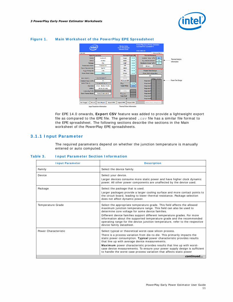
Figure 1. Main Worksheet of the PowerPlay EPE Spreadsheet
Input Parameter Information Thermal Power Information
Thermal AnalysisInformation
Power Tree Design
For EPE 14.0 onwards, Export CSV feature was added to provide a lightweight exportfile as compared to the EPE file. The generated .csv file has a similar file format tothe EPE spreadsheet. The following sections describe the sections in the Mainworksheet of the PowerPlay EPE spreadsheets.
3.1.1 Input Parameter
The required parameters depend on whether the junction temperature is manuallyentered or auto computed.
Table 3. Input Parameter Section Information
Input Parameter Description
Family Select the device family.
Device Select your device.Larger devices consume more static power and have higher clock dynamicpower. All other power components are unaffected by the device used.
Package Select the package that is used.Larger packages provide a larger cooling surface and more contact points tothe circuit board, leading to lower thermal resistance. Package selectiondoes not affect dynamic power.
Temperature Grade Select the appropriate temperature grade. This field affects the allowedmaximum junction temperature range. This field can also be used todetermine core voltage for some device families.Different device families support different temperature grades. For moreinformation about the supported temperature grade and the recommendedoperating range for the device junction temperature, refer to the respectivedevice family datasheet.
Power Characteristic Select typical or theoretical worst-case silicon process.There is a process variation from die-to-die. This primarily impacts thestatic power consumption. Typical power characteristic provides resultsthat line up with average device measurements.Maximum power characteristic provides results that line up with worst-case device measurements. To ensure your power supply design is sufficientto handle the worst-case process variation that affects static power
continued...
3 PowerPlay Early Power Estimator Worksheets
PowerPlay Early Power Estimator User Guide11
Input Parameter Description
consumption, Intel recommends using the Maximum power characteristicfor your power estimation. To enable the Enpirion device selection, youmust set Power Characteristics to Maximum.
VCCINT Voltage (V) For Cyclone IV E devices, select the following VCCINT voltage:• For devices with speed grade C8L, C9L and I8L, set the VCCINT to 1.0V.• For devices with speed grade C6, C7, C8, I7 and A7, set the VCCINT to
1.2V.
VCC_ONE Voltage (V) For MAX 10 devices only, select 3.0 V or 3.3 V. The voltage is internallyregulated to 1.2 V to supply power to the core and periphery.
Power Model Status This shows if the power model for the device is in preliminary or finalversion and is only available from EPE 14.0 onwards.
VCCL Voltage (V) For Stratix III devices, select the following VCCL voltage:• For devices with speed grade –4L, this value can either be 0.9 V or 1.1
V.• For devices with other speed grades, set the VCCL voltage level to 1.1
V.
Junction Temp, TJ (°C) Enter the junction temperature of the device. This field is only available ifyou turn on the User Entered T option. In this case, the junctiontemperature is not calculated based on the thermal information provided.For Enpirion power device selection, Intel recommends setting JunctionTemp, T (°C) to the highest value for the chosen temperature grade.
Ambient Temp, TA (°C) Enter the air temperature near the device. This value can range from –40°C to 125°C. This field is only available when you turn on the AutoComputed T option.If you turn on the Estimated Theta J option, this field is used to computethe junction temperature based on power dissipation and thermalresistance through the top-side cooling solution (heat sink or none) andboard (if applicable).If you turn on the Custom Theta J option, this field is used to computejunction temperature based on power dissipation and custom θJA entered.
Heat Sink Select the heat sink that is used. You can select one of the following:• No heat sink (None)• A custom solution (Custom)• A heat sink with set parameters (15 mm–Low Profile, 23 mm–
Medium Profile, or 28 mm–High Profile). This field is only available ifyou turn on the Auto Computed T and Estimated Theta J options.
If you select None, the heat sink selection updates the custom θSA valueand you can see the value in the Custom θSA (°C/W) parameter. If youselect Custom, the value is what is entered in the Custom θSA (°C/W)parameter.Representative examples of heat sinks are provided. Larger heat sinksprovide lower thermal resistance and lower the junction temperature. If theheat sink is known, consult the heat sink datasheet and enter a custom θSAvalue according to the airflow in your system.
Airflow Select an available ambient airflow in linear-feet per minute (lfm) or metersper second (m/s). The values are 100 lfm (0.5 m/s), 200 lfm (1.0m/s), 400 lfm (2.0 m/s), or Still Air. This field is only available if youturn on the Auto Computed T and Estimated Theta J options.Increased airflow results in a lower case-to-air thermal resistance andlowers the junction temperature.
Custom θJA (°C/W) Enter the junction-to-ambient thermal resistance between the device andambient air (in °C/W). This field is only available if you turn on the followingoptions:
continued...
3 PowerPlay Early Power Estimator Worksheets
PowerPlay Early Power Estimator User Guide12
Input Parameter Description
• Auto Computed T• Estimated Theta J• Set the Heat Sink parameter to CustomTo compute the overall junction-to-ambient resistance through the top ofthe device, the Custom θSA parameter is combined with a representativecase-to-heatsink resistance and an Intel-provided junction-to-case thermalresistance.
Board Thermal Mode Select the type of board that is used in the thermal analysis. The value isNone (Conservative), Typical Board, or JEDEC (2s2p). This field isonly available if you turn on the Auto Computed T and Estimated ThetaJ options.If you select None (Conservative), the thermal model assumes no heat isdissipated through the board, resulting in a pessimistic calculated junctiontemperature. This option is not available if the Heat Sink option is set toNone.If you select Typical Board, the thermal model assumes the characteristicsof a typical customer board stack, which is based on the selected deviceand package.If you select JEDEC (2s2p), the thermal model assumes the characteristicsof the JEDEC 2s2p test board specified in standard JESDEC51–9.To determine the final junction temperature, Intel recommends performinga detailed thermal simulation of your system. This two-resistor thermalmodel is only for early estimation.
3.1.2 Thermal Power
Thermal power is the power dissipated in the device. Total thermal power is a sum ofthe thermal power of all the resources used in the device, including the maximumpower from standby and dynamic power.
Total thermal power only includes the thermal component for the I/O section and doesnot include the external power dissipation, such as from voltage-referencedtermination resistors.
The static power (PSTATIC) is the thermal power dissipated on chip, independent of userclocks. PSTATIC includes the leakage power from all FPGA functional blocks, except forI/O DC bias power and transceiver DC bias power, which are accounted for in the I/Oand transceiver sections.
PSTATIC is the only thermal power component which varies with junction temperature,selected device, and power characteristics (process).
The following figure shows the total thermal power (W) and PSTATIC consumed by theFPGA and hard processor system (HPS). The thermal power for each worksheet isdisplayed. To see how the thermal power for a worksheet was calculated, click on thebutton to view the selected worksheet.
3 PowerPlay Early Power Estimator Worksheets
PowerPlay Early Power Estimator User Guide13
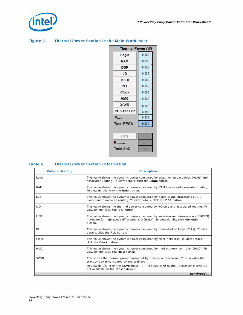
Figure 2. Thermal Power Section in the Main Worksheet
Table 4. Thermal Power Section Information
Column Heading Description
Logic This value shows the dynamic power consumed by adaptive logic modules (ALMs) andassociated routing. To view details, click the Logic button.
RAM This value shows the dynamic power consumed by RAM blocks and associated routing.To view details, click the RAM button.
DSP This value shows the dynamic power consumed by digital signal processing (DSP)blocks and associated routing. To view details, click the DSP button.
I/O This value shows the thermal power consumed by I/O pins and associated routing. Toview details, click the I/O button.
HSDI This value shows the dynamic power consumed by serializer and deserializer (SERDES)hardware for high-speed differential I/O (HSDI). To view details, click the HSDIbutton.
PLL This value shows the dynamic power consumed by phase-locked loops (PLLs). To viewdetails, click the PLL button.
Clock This value shows the dynamic power consumed by clock networks. To view details,click the Clock button.
HMC This value shows the dynamic power consumed by hard memory controller (HMC). Toview details, click the HMC button.
XCVR This shows the thermal power consumed by transceiver hardware. This includes thestandby power consumed by transceivers.To view details, click the XCVR button. If the value is N/A, the transceiver blocks arenot available on the chosen device.
continued...
3 PowerPlay Early Power Estimator Worksheets
PowerPlay Early Power Estimator User Guide14
Column Heading Description
PCS and HIP This shows the thermal power consumed by the transceiver channel physical codingsublayer (PCS) as well as the PCI Express® (PCIe®) hard IP blocks of the transceiverhardware. This includes the standby power consumed by transceivers.To view details, click the PCS and HIP button. If the value is N/A, the transceiverblocks are not available on the chosen device.
PSTATIC This shows the thermal power dissipated on chip, independent of user clocks. Thisincludes the leakage power from all FPGA functional blocks, except for I/O DC biaspower and transceiver DC bias power.PSTATIC is affected by junction temperature, selected device, and power characteristics.The static power for HPS is shown in PSTATIC,HPS.
Total FPGA This shows the total power dissipated as heat from the FPGA. This does not includepower dissipated in off-chip termination resistors and HPS.
HPS This value shows the thermal power consumed by the HPS. To view the details, clickthe HPS button.
PSTATIC,HPS This shows the thermal power dissipated from the HPS, independent of user clocks.This includes the leakage power from all HPS functional blocks, except for HPS I/O DCbias power.PSTATIC,HPS is affected by junction temperature, selected device, and powercharacteristics. The static power for HPS will be turned on once the SoC device isselected.
Total SoC This value shows the total power dissipated as heat from the FPGA and HPS. This valuedoes not include power dissipated in off-chip termination resistors.
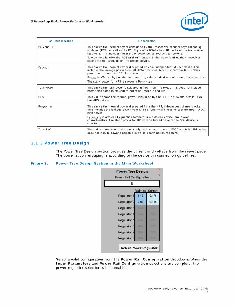
3.1.3 Power Tree Design
The Power Tree Design section provides the current and voltage from the report page.The power supply grouping is according to the device pin connection guidelines.
Figure 3. Power Tree Design Section in the Main Worksheet
Select a valid configuration from the Power Rail Configuration dropdown. When theInput Parameters and Power Rail Configuration selections are complete, thepower regulator selection will be enabled.
3 PowerPlay Early Power Estimator Worksheets
PowerPlay Early Power Estimator User Guide15
The current values shown for each regulator include the margin for regulator selectionpurpose. For more information, refer to the Enpirion worksheet.
Errors regarding improper rail grouping may appear in the error window on the Mainworksheet when the Power Rail Configuration is selected. The following figure showsan example of the error message in the error window.
Figure 4. Error Window in the Main Worksheet
This occurs when the EPE assigns rails with different voltage requirements to the samegroup. Since each group is supplied by a single regulator, these errors must becorrected before the EPE can make proper component selections. This is done in theEPE Report worksheet. Refer to the Report worksheet on how to correct the error.
Related Links
• Report Worksheet on page 41
• Enpirion Worksheet on page 42
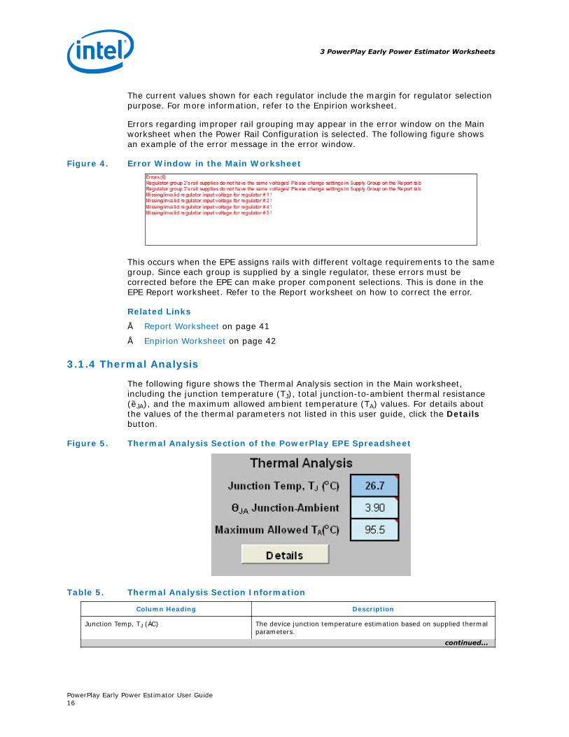
3.1.4 Thermal Analysis
The following figure shows the Thermal Analysis section in the Main worksheet,including the junction temperature (TJ), total junction-to-ambient thermal resistance(θJA), and the maximum allowed ambient temperature (TA) values. For details aboutthe values of the thermal parameters not listed in this user guide, click the Detailsbutton.
Figure 5. Thermal Analysis Section of the PowerPlay EPE Spreadsheet
Table 5. Thermal Analysis Section Information
Column Heading Description
Junction Temp, TJ (°C) The device junction temperature estimation based on supplied thermalparameters.
continued...
3 PowerPlay Early Power Estimator Worksheets
PowerPlay Early Power Estimator User Guide16
Column Heading Description
The junction temperature is determined by dissipating the totalthermal power through the top of the chip and through the board (ifselected). For detailed calculations, click the Details button.
θJA Junction-Ambient The junction-to-ambient thermal resistance between the device andambient air (in °C/W).Represents the increase in temperature between ambient and junctionfor every W of additional power dissipation.
Maximum Allowed TA (°C) A guideline for the maximum ambient temperature (in °C) that you cansubject the device to without violating the maximum junctiontemperature, based on the supplied cooling solution and devicetemperature grade.
You can directly enter or automatically compute the junction temperature based onthe information provided. To enter the junction temperature, select User Entered T inthe Input Parameters section. To automatically compute the junction temperature,select Auto Computed T in the Input Parameters section.
When automatically computing the junction temperature, the ambient temperature,airflow, heat sink solution, and board thermal model of the device determine thejunction temperature in °C. Junction temperature is the estimated operating junctiontemperature based on your device and thermal conditions.
You can consider the device as a heat source and the junction temperature is thetemperature of the device. While the temperature typically varies across the device, tosimplify the analysis, you can assume that the temperature of the device is constantregardless of where it is measured.
Power from the device can be dissipated through different paths. Different pathsbecome significant depending on the thermal properties of the system. Thesignificance of power dissipation paths vary depending on whether or not a heat sinkis used for the device.
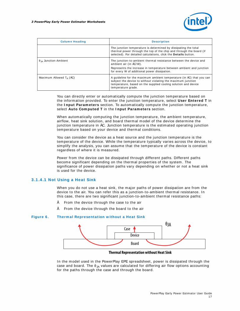
3.1.4.1 Not Using a Heat Sink
When you do not use a heat sink, the major paths of power dissipation are from thedevice to the air. You can refer this as a junction-to-ambient thermal resistance. Inthis case, there are two significant junction-to-ambient thermal resistance paths:
• From the device through the case to the air
• From the device through the board to the air
Figure 6. Thermal Representation without a Heat Sink
Case
Thermal Representation without Heat Sink
Board
Device
θJA
In the model used in the PowerPlay EPE spreadsheet, power is dissipated through thecase and board. The θJA values are calculated for differing air flow options accountingfor the paths through the case and through the board.
3 PowerPlay Early Power Estimator Worksheets
PowerPlay Early Power Estimator User Guide17
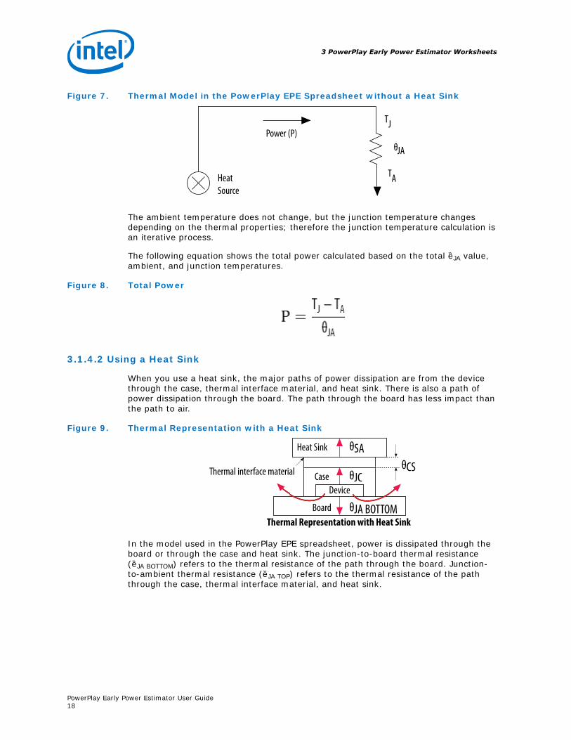
Figure 7. Thermal Model in the PowerPlay EPE Spreadsheet without a Heat Sink
TJ
JA
TA
Power (P)
HeatSource
θ
The ambient temperature does not change, but the junction temperature changesdepending on the thermal properties; therefore the junction temperature calculation isan iterative process.
The following equation shows the total power calculated based on the total θJA value,ambient, and junction temperatures.
Figure 8. Total Power
3.1.4.2 Using a Heat Sink
When you use a heat sink, the major paths of power dissipation are from the devicethrough the case, thermal interface material, and heat sink. There is also a path ofpower dissipation through the board. The path through the board has less impact thanthe path to air.
Figure 9. Thermal Representation with a Heat Sink
Heat Sink
CaseDevice
Board
Thermal interface material
θJA BOTTOM
θJC
θSA
Thermal Representation with Heat Sink
θCS
In the model used in the PowerPlay EPE spreadsheet, power is dissipated through theboard or through the case and heat sink. The junction-to-board thermal resistance(θJA BOTTOM) refers to the thermal resistance of the path through the board. Junction-to-ambient thermal resistance (θJA TOP) refers to the thermal resistance of the paththrough the case, thermal interface material, and heat sink.
3 PowerPlay Early Power Estimator Worksheets
PowerPlay Early Power Estimator User Guide18
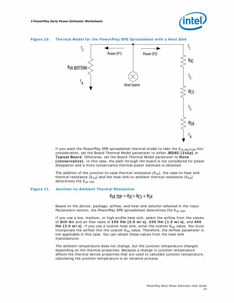
Figure 10. Thermal Model for the PowerPlay EPE Spreadsheet with a Heat Sink
TJ
TA
Power (P1)
Heat Source
Power (P2)
TJ
TC
TS
TA
θJA BOTTOM
θJC
θCS
θSA
If you want the PowerPlay EPE spreadsheet thermal model to take the θJA BOTTOM intoconsideration, set the Board Thermal Model parameter to either JEDEC (2s2p) orTypical Board. Otherwise, set the Board Thermal Model parameter to None(conservative). In this case, the path through the board is not considered for powerdissipation and a more conservative thermal power estimate is obtained.
The addition of the junction-to-case thermal resistance (θJC), the case-to-heat sinkthermal resistance (θCS) and the heat sink-to-ambient thermal resistance (θSA)determines the θJA TOP.
Figure 11. Junction-to-Ambient Thermal Resistance
θJA TOP = θJC+ θCS + θSA
Based on the device, package, airflow, and heat sink solution selected in the InputParameters section, the PowerPlay EPE spreadsheet determines the θJA TOP.
If you use a low, medium, or high profile heat sink, select the airflow from the valuesof Still Air and air flow rates of 100 lfm (0.5 m/s), 200 lfm (1.0 m/s), and 400lfm (2.0 m/s). If you use a custom heat sink, enter the custom θSA value. You mustincorporate the airflow into the custom θSA value. Therefore, the Airflow parameter isnot applicable in this case. You can obtain these values from the heat sinkmanufacturer.
The ambient temperature does not change, but the junction temperature changesdepending on the thermal properties. Because a change in junction temperatureaffects the thermal device properties that are used to calculate junction temperature,calculating the junction temperature is an iterative process.
3 PowerPlay Early Power Estimator Worksheets
PowerPlay Early Power Estimator User Guide19
The total power is calculated based on the total θJA value, ambient, and junctiontemperatures with the following equation.
Figure 12. Total Power
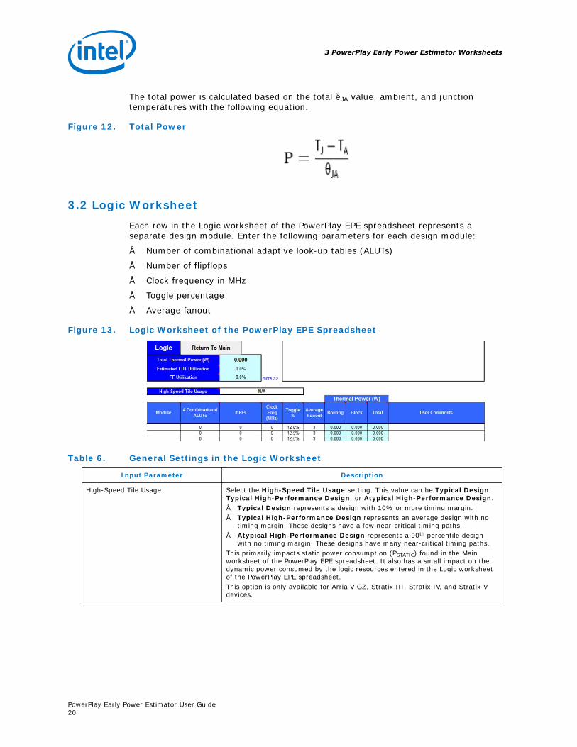
3.2 Logic Worksheet
Each row in the Logic worksheet of the PowerPlay EPE spreadsheet represents aseparate design module. Enter the following parameters for each design module:
• Number of combinational adaptive look-up tables (ALUTs)
• Number of flipflops
• Clock frequency in MHz
• Toggle percentage
• Average fanout
Figure 13. Logic Worksheet of the PowerPlay EPE Spreadsheet
Table 6. General Settings in the Logic Worksheet
Input Parameter Description
High-Speed Tile Usage Select the High-Speed Tile Usage setting. This value can be Typical Design,Typical High-Performance Design, or Atypical High-Performance Design.• Typical Design represents a design with 10% or more timing margin.• Typical High-Performance Design represents an average design with no
timing margin. These designs have a few near-critical timing paths.• Atypical High-Performance Design represents a 90th percentile design
with no timing margin. These designs have many near-critical timing paths.This primarily impacts static power consumption (PSTATIC) found in the Mainworksheet of the PowerPlay EPE spreadsheet. It also has a small impact on thedynamic power consumed by the logic resources entered in the Logic worksheetof the PowerPlay EPE spreadsheet.This option is only available for Arria V GZ, Stratix III, Stratix IV, and Stratix Vdevices.
3 PowerPlay Early Power Estimator Worksheets
PowerPlay Early Power Estimator User Guide20
Table 7. Logic Worksheet Information
Column Heading Description
Module Specify a name for each module of the design. This is an optional entry.
#Combinational ALUTs/#LUTs Enter the number of combinational ALUTs or look-up tables (LUTs).This is the “Combinational ALUTs” value from the Quartus II Compilation ReportResource Usage Summary section.For Arria II, Arria V GZ, Stratix III, Stratix IV, and Stratix V devices, eachadaptive logic module (ALM) contains up to two combinational ALUTs. SmallerALUTs consume less power than larger ALUTs, but the device can fit more ofthem. The total number of ALUTs in the design must not exceed (the number ofALMs) × two.
#FFs Enter the number of flipflops in the module.This is the sum of “Register ALUTs” and “Dedicated logic registers” from theQuartus II Compilation Report Resource Usage Summary section.Clock routing power is calculated separately on the Clock worksheet of thePowerPlay EPE spreadsheet.
Clock Freq (MHz) Enter a clock frequency (in MHz). This value is limited by the maximumfrequency specification for the device family.100 MHz with a 12.5% toggle means that each LUT or flipflop output toggles12.5 million times per second (100 × 12.5%).
Toggle% Enter the average percentage of logic toggling on each clock cycle. The togglepercentage ranges from 0 to 100%. Typically, the toggle percentage is 12.5%,which is the toggle percentage of a 16-bit counter. To ensure you do notunderestimate the toggle percentage, use a higher toggle percentage. Most logiconly toggles infrequently; therefore, toggle rates of less than 50% are morerealistic.For example, a T-flipflop (TFF) with its input tied to VCC has a toggle rate of100% because its output is changing logic states on every clock cycle. Refer tothe 4-Bit Counter Example.
Average Fanout Enter the average number of blocks fed by the outputs of the LUTs and flipflops.
Thermal Power (W)–Routing This shows the power dissipation due to estimated routing (in watts).Routing power depends on placement and routing, which is a function of designcomplexity. The values shown represent the routing power based onexperimentation of more than 100 designs.For detailed analysis based on your design’s routing, use the Quartus IIPowerPlay Analyzer.
Thermal Power (W)–Block This shows the power dissipation due to internal toggling of the ALMs (in watts).Logic block power is a combination of the function implemented and the relativetoggle rates of the various inputs. The PowerPlay EPE spreadsheet uses anestimate based on observed behavior across more than 100 real-world designs.For accurate analysis based on your design’s exact synthesis, use the Quartus IIPowerPlay Analyzer.
Thermal Power (W)–Total This shows the total power dissipation (in watts). The total power dissipation isthe sum of the routing and block power.
User Comments Enter any comments. This is an optional entry.
3 PowerPlay Early Power Estimator Worksheets
PowerPlay Early Power Estimator User Guide21
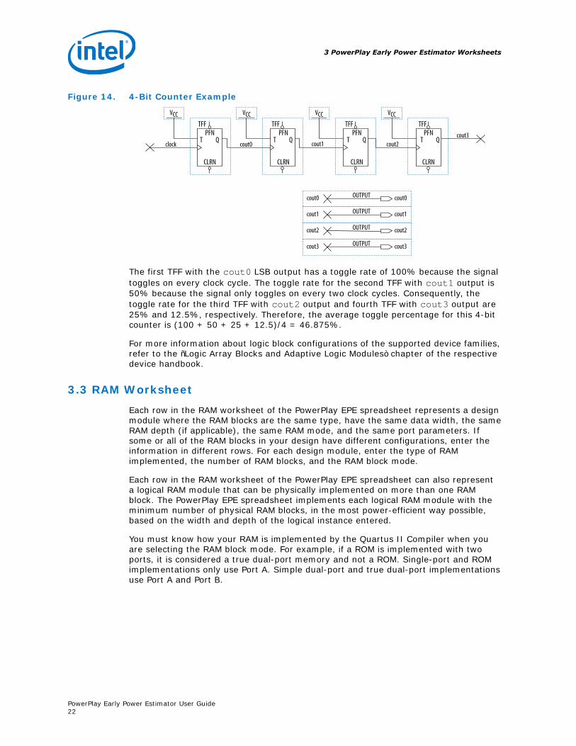
Figure 14. 4-Bit Counter Example
TFFPFN
T Q
CLRN
TFFPFN
T Q
CLRN
TFFPFN
T Q
CLRN
TFFPFN
T Q
CLRN
VCC VCC VCCVCC
cout2cout1cout0clockcout3
OUTPUT cout0cout0
OUTPUT cout3cout3
OUTPUT cout2cout2
OUTPUT cout1cout1
The first TFF with the cout0 LSB output has a toggle rate of 100% because the signaltoggles on every clock cycle. The toggle rate for the second TFF with cout1 output is50% because the signal only toggles on every two clock cycles. Consequently, thetoggle rate for the third TFF with cout2 output and fourth TFF with cout3 output are25% and 12.5%, respectively. Therefore, the average toggle percentage for this 4-bitcounter is (100 + 50 + 25 + 12.5)/4 = 46.875%.
For more information about logic block configurations of the supported device families,refer to the “Logic Array Blocks and Adaptive Logic Modules” chapter of the respectivedevice handbook.
3.3 RAM Worksheet
Each row in the RAM worksheet of the PowerPlay EPE spreadsheet represents a designmodule where the RAM blocks are the same type, have the same data width, the sameRAM depth (if applicable), the same RAM mode, and the same port parameters. Ifsome or all of the RAM blocks in your design have different configurations, enter theinformation in different rows. For each design module, enter the type of RAMimplemented, the number of RAM blocks, and the RAM block mode.
Each row in the RAM worksheet of the PowerPlay EPE spreadsheet can also representa logical RAM module that can be physically implemented on more than one RAMblock. The PowerPlay EPE spreadsheet implements each logical RAM module with theminimum number of physical RAM blocks, in the most power-efficient way possible,based on the width and depth of the logical instance entered.
You must know how your RAM is implemented by the Quartus II Compiler when youare selecting the RAM block mode. For example, if a ROM is implemented with twoports, it is considered a true dual-port memory and not a ROM. Single-port and ROMimplementations only use Port A. Simple dual-port and true dual-port implementationsuse Port A and Port B.
3 PowerPlay Early Power Estimator Worksheets
PowerPlay Early Power Estimator User Guide22
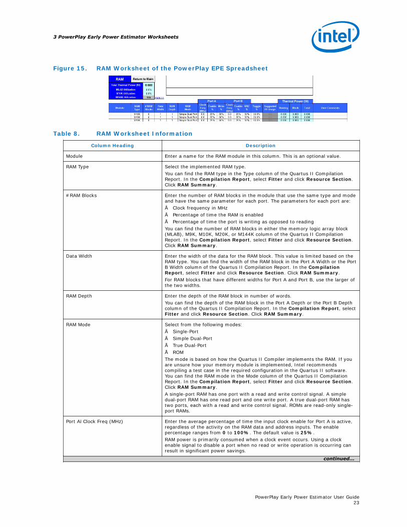
Figure 15. RAM Worksheet of the PowerPlay EPE Spreadsheet
Table 8. RAM Worksheet Information
Column Heading Description
Module Enter a name for the RAM module in this column. This is an optional value.
RAM Type Select the implemented RAM type.You can find the RAM type in the Type column of the Quartus II CompilationReport. In the Compilation Report, select Fitter and click Resource Section.Click RAM Summary.
#RAM Blocks Enter the number of RAM blocks in the module that use the same type and modeand have the same parameter for each port. The parameters for each port are:• Clock frequency in MHz• Percentage of time the RAM is enabled• Percentage of time the port is writing as opposed to readingYou can find the number of RAM blocks in either the memory logic array block(MLAB), M9K, M10K, M20K, or M144K column of the Quartus II CompilationReport. In the Compilation Report, select Fitter and click Resource Section.Click RAM Summary.
Data Width Enter the width of the data for the RAM block. This value is limited based on theRAM type. You can find the width of the RAM block in the Port A Width or the PortB Width column of the Quartus II Compilation Report. In the CompilationReport, select Fitter and click Resource Section. Click RAM Summary.For RAM blocks that have different widths for Port A and Port B, use the larger ofthe two widths.
RAM Depth Enter the depth of the RAM block in number of words.You can find the depth of the RAM block in the Port A Depth or the Port B Depthcolumn of the Quartus II Compilation Report. In the Compilation Report, selectFitter and click Resource Section. Click RAM Summary.
RAM Mode Select from the following modes:• Single-Port• Simple Dual-Port• True Dual-Port• ROMThe mode is based on how the Quartus II Compiler implements the RAM. If youare unsure how your memory module is implemented, Intel recommendscompiling a test case in the required configuration in the Quartus II software.You can find the RAM mode in the Mode column of the Quartus II CompilationReport. In the Compilation Report, select Fitter and click Resource Section.Click RAM Summary.A single-port RAM has one port with a read and write control signal. A simpledual-port RAM has one read port and one write port. A true dual-port RAM hastwo ports, each with a read and write control signal. ROMs are read-only single-port RAMs.
Port A–Clock Freq (MHz) Enter the average percentage of time the input clock enable for Port A is active,regardless of the activity on the RAM data and address inputs. The enablepercentage ranges from 0 to 100%. The default value is 25%.RAM power is primarily consumed when a clock event occurs. Using a clockenable signal to disable a port when no read or write operation is occurring canresult in significant power savings.
continued...
3 PowerPlay Early Power Estimator Worksheets
PowerPlay Early Power Estimator User Guide23
Column Heading Description
Port A–Write % Enter the average percentage of time Port A of the RAM block is in write modeversus read mode. For simple dual-port (1R/1W) RAMs, the write Port A isinactive when not executing a write operation. For single-port and dual-portRAMs, Port A reads when it is not written to. This field is ignored for RAMs inROM mode.This value must be a percentage number between 0 and 100%. The defaultvalue is 50%.
Port B–Clock Freq (MHz) Enter the clock frequency for Port B of the RAM blocks in MHz. This value islimited by the maximum frequency specification for the RAM type and devicefamily. Port B is ignored for RAM blocks in ROM or single-port mode or when thechosen RAM type is MLAB.
Port B–Enable % Enter the average percentage of time the input clock enable for Port B is active,regardless of the activity on the RAM data and address inputs. The enablepercentage ranges from 0 to 100%. The default value is 25%. Port B is ignoredfor RAM blocks in ROM or single-port mode or when the chosen RAM type isMLAB.RAM power is primarily consumed when a clock event occurs. Using a clock-enable signal to disable a port when no read or write operation is occurring canresult in significant power savings.
Port B–R/W % For RAM blocks in true dual-port mode, enter the average percentage of timePort B of the RAM block is in write mode versus read mode. For RAM blocks insimple dual-port mode, enter the percentage of time Port B of the RAM block isreading. You cannot write to Port B in simple dual-port mode. Port B is ignoredfor RAM blocks in ROM or single-port mode or when the chosen RAM type isMLAB.This value must be a percentage number between 0 and 100%. The defaultvalue is 50%.
Toggle% The average percentage for how often each block output signal changes value oneach clock cycle is multiplied by the clock frequency and enables the percentageto determine the number of transitions per second. This only affects routingpower.50% corresponds to a randomly changing signal. A random signal changes statesonly half the time.
Suggested FF Usage Displays the number of flipflops that you require to make the MLAB functioncorrectly. The MLAB power in the RAM worksheet does not include the power ofthe flipflops.If you enter the device resources manually, add the suggested number offlipflops to the Logic worksheet using the same clock frequency.If you have imported the device resources from the PowerPlay EPE file, no actionis required.This field is only valid when the chosen RAM type is MLAB.
Thermal Power (W)–Routing This shows the power dissipation due to estimated routing (in watts).Routing power depends on placement and routing, which is a function of designcomplexity. The values shown represent the routing power based onexperimentation of more than 100 designs.For detailed analysis based on your design’s routing, use the Quartus IIPowerPlay Power Analyzer. This value is automatically calculated.
Thermal Power (W)–Block This shows the power dissipation due to internal toggling of the RAM (in watts).For accurate analysis based on your design’s exact RAM modes, use the QuartusII PowerPlay Power Analyzer. This value is automatically calculated.
Thermal Power (W)–Total This shows the estimated power in watts, based on your inputs. It is the totalpower consumed by the RAM blocks and is equal to the routing power and blockpower. This value is automatically calculated.
User Comments Enter any comments. This is an optional entry.
For more information about the RAM block configurations of the supported devicefamilies, refer to the “Memory Blocks” chapter of the respective device handbook.
3 PowerPlay Early Power Estimator Worksheets
PowerPlay Early Power Estimator User Guide24
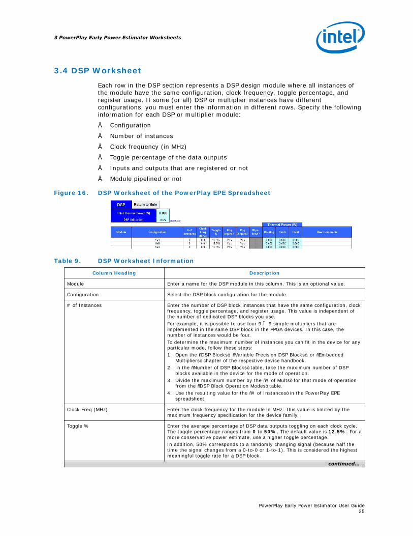
3.4 DSP Worksheet
Each row in the DSP section represents a DSP design module where all instances ofthe module have the same configuration, clock frequency, toggle percentage, andregister usage. If some (or all) DSP or multiplier instances have differentconfigurations, you must enter the information in different rows. Specify the followinginformation for each DSP or multiplier module:
• Configuration
• Number of instances
• Clock frequency (in MHz)
• Toggle percentage of the data outputs
• Inputs and outputs that are registered or not
• Module pipelined or not
Figure 16. DSP Worksheet of the PowerPlay EPE Spreadsheet
Table 9. DSP Worksheet Information
Column Heading Description
Module Enter a name for the DSP module in this column. This is an optional value.
Configuration Select the DSP block configuration for the module.
# of Instances Enter the number of DSP block instances that have the same configuration, clockfrequency, toggle percentage, and register usage. This value is independent ofthe number of dedicated DSP blocks you use.For example, it is possible to use four 9 × 9 simple multipliers that areimplemented in the same DSP block in the FPGA devices. In this case, thenumber of instances would be four.To determine the maximum number of instances you can fit in the device for anyparticular mode, follow these steps:1. Open the “DSP Blocks”, “Variable Precision DSP Blocks”, or “Embedded
Multipliers” chapter of the respective device handbook.2. In the “Number of DSP Blocks” table, take the maximum number of DSP
blocks available in the device for the mode of operation.3. Divide the maximum number by the “# of Mults” for that mode of operation
from the “DSP Block Operation Modes” table.4. Use the resulting value for the “# of Instances” in the PowerPlay EPE
spreadsheet.
Clock Freq (MHz) Enter the clock frequency for the module in MHz. This value is limited by themaximum frequency specification for the device family.
Toggle % Enter the average percentage of DSP data outputs toggling on each clock cycle.The toggle percentage ranges from 0 to 50%. The default value is 12.5%. For amore conservative power estimate, use a higher toggle percentage.In addition, 50% corresponds to a randomly changing signal (because half thetime the signal changes from a 0-to-0 or 1-to-1). This is considered the highestmeaningful toggle rate for a DSP block.
continued...
3 PowerPlay Early Power Estimator Worksheets
PowerPlay Early Power Estimator User Guide25
Column Heading Description
Reg Inputs? Select whether the inputs of the dedicated DSP block or multiplier block areregistered using the dedicated input registers. If you use the dedicated inputregisters in the DSP or multiplier block, select Yes. If the inputs are unregisteredor registered using registers in the ALMs or the look-up table (LUTs), select No.
Reg Outputs? Select whether the outputs of the dedicated DSP block or multiplier block areregistered using the dedicated input registers. If you use the dedicated outputregisters in the DSP or multiplier block, select Yes. If the inputs are unregisteredor registered using registers in ALMs or LUTs, select No.
Pipelined? Select whether or not the dedicated DSP block is pipelined.
Thermal Power (W)–Routing This shows the power dissipation due to estimated routing (in watts).Routing power depends on placement and routing, which is a function of designcomplexity. The values shown represent the routing power based onexperimentation of more than 100 designs.
Thermal Power (W)–Block This shows the estimated power consumed by the DSP blocks (in watts). Thisvalue is automatically calculated.
Thermal Power (W)–Total This shows the estimated power (in watts), based on your inputs. It is the totalpower consumed by the DSP blocks and is equal to the routing power and blockpower. This value is automatically calculated.
User Comments Enter any comments. This is an optional entry.
For more information about the DSP block configurations of the supported devicefamilies, refer to the “DSP Blocks”, “Variable Precision DSP Blocks”, or “EmbeddedMultipliers” chapter of the respective device handbook.
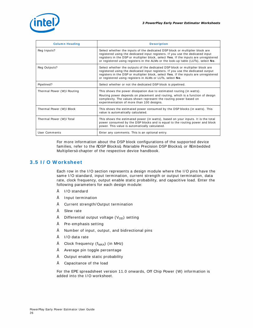
3.5 I/O Worksheet
Each row in the I/O section represents a design module where the I/O pins have thesame I/O standard, input termination, current strength or output termination, datarate, clock frequency, output enable static probability, and capacitive load. Enter thefollowing parameters for each design module:
• I/O standard
• Input termination
• Current strength/Output termination
• Slew rate
• Differential output voltage (VOD) setting
• Pre-emphasis setting
• Number of input, output, and bidirectional pins
• I/O data rate
• Clock frequency (fMAX) (in MHz)
• Average pin toggle percentage
• Output enable static probability
• Capacitance of the load
For the EPE spreadsheet version 11.0 onwards, Off Chip Power (W) information isadded into the I/O worksheet.
3 PowerPlay Early Power Estimator Worksheets
PowerPlay Early Power Estimator User Guide26
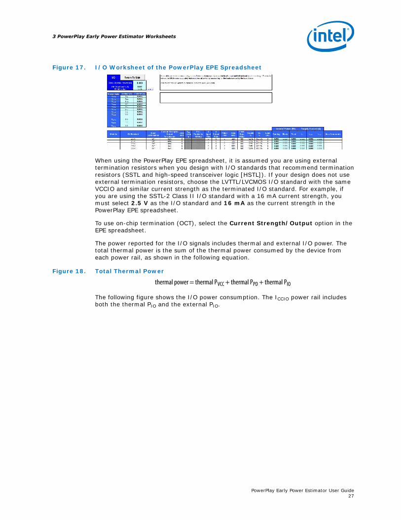
Figure 17. I/O Worksheet of the PowerPlay EPE Spreadsheet
When using the PowerPlay EPE spreadsheet, it is assumed you are using externaltermination resistors when you design with I/O standards that recommend terminationresistors (SSTL and high-speed transceiver logic [HSTL]). If your design does not useexternal termination resistors, choose the LVTTL/LVCMOS I/O standard with the sameVCCIO and similar current strength as the terminated I/O standard. For example, ifyou are using the SSTL-2 Class II I/O standard with a 16 mA current strength, youmust select 2.5 V as the I/O standard and 16 mA as the current strength in thePowerPlay EPE spreadsheet.
To use on-chip termination (OCT), select the Current Strength/Output option in theEPE spreadsheet.
The power reported for the I/O signals includes thermal and external I/O power. Thetotal thermal power is the sum of the thermal power consumed by the device fromeach power rail, as shown in the following equation.
Figure 18. Total Thermal Power
thermal power = thermal PVCC + thermal PPD + thermal PIO
The following figure shows the I/O power consumption. The ICCIO power rail includesboth the thermal PIO and the external PIO.
3 PowerPlay Early Power Estimator Worksheets
PowerPlay Early Power Estimator User Guide27
Figure 19. I/O Power Representation
VCC VCCPD VCCIO
ICC ICCPD ICCIO
Thermal PVCC Thermal PPD Thermal PIO External PIO
Stratix III Device
The VREF pins consume minimal current (typically less than 10 μA) and is negligiblewhen compared with the current consumed by the general purpose I/O (GPIO) pins;therefore, the PowerPlay EPE spreadsheet does not include the current for VREF pinsin the calculations.
Table 10. I/O Power Rail Information
Column Heading Description
Power Rails Power supply rails for the I/O pins.
Voltage (V) The voltage applied to the specified power rail in Volts (V).
Current (A) The current drawn from the specified power rail in Amps (A).
Table 11. I/O Worksheet Information
Column Heading Description
Module Specify a name for the module in this column. This is an optionalvalue.
I/O Standard Select the I/O standard used for the input, output, or bidirectionalpins in this module from the drop-down list.The calculated I/O power varies based on the I/O standard. For I/Ostandards that recommend termination (SSTL and HSTL), thePowerPlay EPE spreadsheet assumes you are using externaltermination resistors. If you are not using external terminationresistors, choose the LVTTL/LVCMOS I/O standard with the samevoltage and current strength as the terminated I/O standard.To view all the I/O standards in the drop-down list, use the scroll bar.
Input Termination Select the input termination (on-chip parallel termination [RT OCT] oron-chip differential termination [RD OCT]) setting implemented forthe input and bidirectional pins in this module.
Current Strength/ Output Termination Select the current strength or output termination (on-chip serialtermination [RS OCT]) implemented for the output and bidirectionalpins in this module.Current strength and output termination are mutually exclusive.
continued...
3 PowerPlay Early Power Estimator Worksheets
PowerPlay Early Power Estimator User Guide28
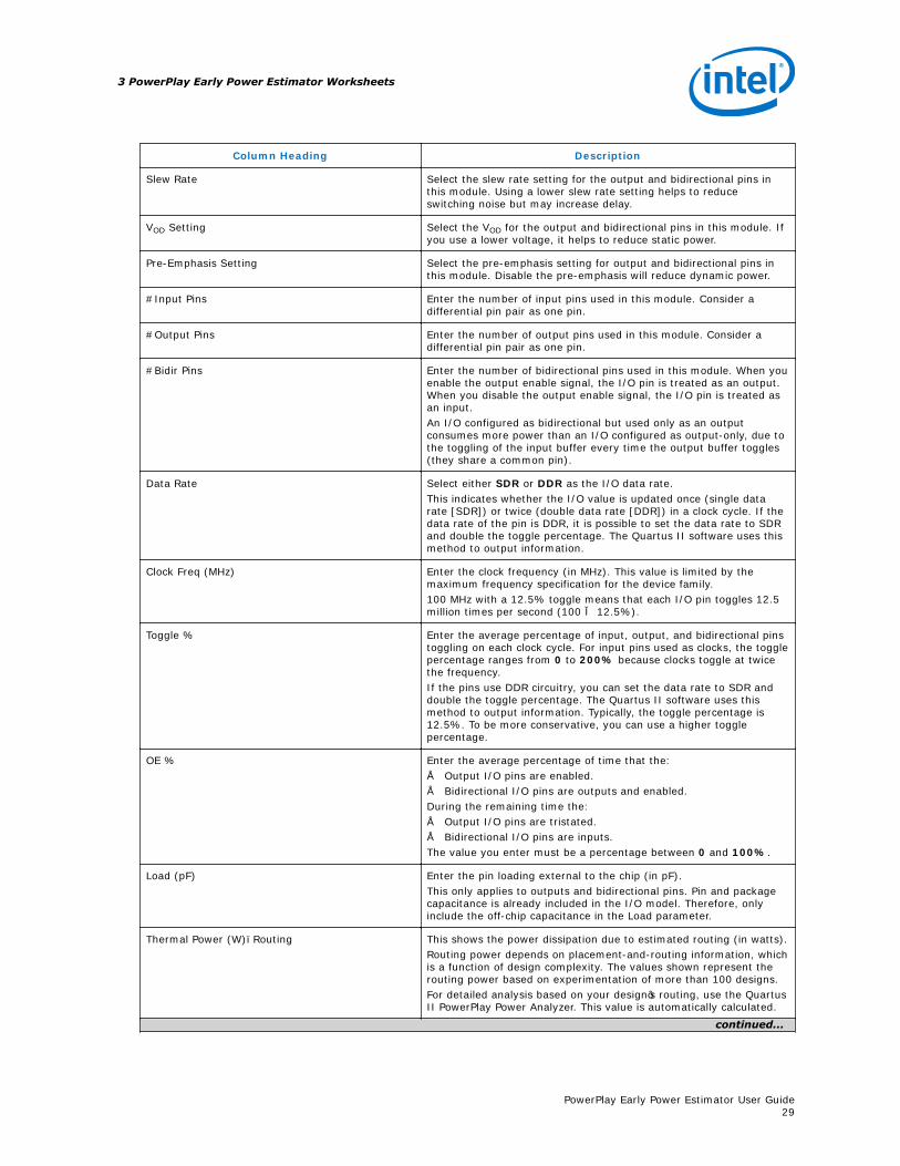
Column Heading Description
Slew Rate Select the slew rate setting for the output and bidirectional pins inthis module. Using a lower slew rate setting helps to reduceswitching noise but may increase delay.
VOD Setting Select the VOD for the output and bidirectional pins in this module. Ifyou use a lower voltage, it helps to reduce static power.
Pre-Emphasis Setting Select the pre-emphasis setting for output and bidirectional pins inthis module. Disable the pre-emphasis will reduce dynamic power.
#Input Pins Enter the number of input pins used in this module. Consider adifferential pin pair as one pin.
#Output Pins Enter the number of output pins used in this module. Consider adifferential pin pair as one pin.
#Bidir Pins Enter the number of bidirectional pins used in this module. When youenable the output enable signal, the I/O pin is treated as an output.When you disable the output enable signal, the I/O pin is treated asan input.An I/O configured as bidirectional but used only as an outputconsumes more power than an I/O configured as output-only, due tothe toggling of the input buffer every time the output buffer toggles(they share a common pin).
Data Rate Select either SDR or DDR as the I/O data rate.This indicates whether the I/O value is updated once (single datarate [SDR]) or twice (double data rate [DDR]) in a clock cycle. If thedata rate of the pin is DDR, it is possible to set the data rate to SDRand double the toggle percentage. The Quartus II software uses thismethod to output information.
Clock Freq (MHz) Enter the clock frequency (in MHz). This value is limited by themaximum frequency specification for the device family.100 MHz with a 12.5% toggle means that each I/O pin toggles 12.5million times per second (100 × 12.5%).
Toggle % Enter the average percentage of input, output, and bidirectional pinstoggling on each clock cycle. For input pins used as clocks, the togglepercentage ranges from 0 to 200% because clocks toggle at twicethe frequency.If the pins use DDR circuitry, you can set the data rate to SDR anddouble the toggle percentage. The Quartus II software uses thismethod to output information. Typically, the toggle percentage is12.5%. To be more conservative, you can use a higher togglepercentage.
OE % Enter the average percentage of time that the:• Output I/O pins are enabled.• Bidirectional I/O pins are outputs and enabled.During the remaining time the:• Output I/O pins are tristated.• Bidirectional I/O pins are inputs.The value you enter must be a percentage between 0 and 100%.
Load (pF) Enter the pin loading external to the chip (in pF).This only applies to outputs and bidirectional pins. Pin and packagecapacitance is already included in the I/O model. Therefore, onlyinclude the off-chip capacitance in the Load parameter.
Thermal Power (W)–Routing This shows the power dissipation due to estimated routing (in watts).Routing power depends on placement-and-routing information, whichis a function of design complexity. The values shown represent therouting power based on experimentation of more than 100 designs.For detailed analysis based on your design’s routing, use the QuartusII PowerPlay Power Analyzer. This value is automatically calculated.
continued...
3 PowerPlay Early Power Estimator Worksheets
PowerPlay Early Power Estimator User Guide29
Column Heading Description
Thermal Power (W)–Block This shows the power dissipation due to internal and load toggling ofthe I/O (in watts).For accurate analysis based on your design’s exact I/O configuration,use the Quartus II PowerPlay Power Analyzer. This value isautomatically calculated.
Thermal Power (W)–Total This shows the total power dissipation (in watts). The total powerdissipation is the sum of the routing and block power. This value isautomatically calculated.
Supply Current (A)–ICC This shows the current drawn from the VCC power rail and powers theinternal digital circuitry. This value is automatically calculated.
Supply Current (A)–ICCPD This shows the current drawn from the VCCPD power rail and powersthe pre-drive circuitry. This value is automatically calculated.
Supply Current (A)–ICCIO This shows the current drawn from the VCCIO power rail. Some of thiscurrent may be drawn into off-chip termination resistors. This valueis automatically calculated.
User Comments Enter any comments. This is an optional entry.
For more information about the I/O standard termination scheme of the supporteddevice families, refer to the “I/O Features” chapter of the respective device handbook.
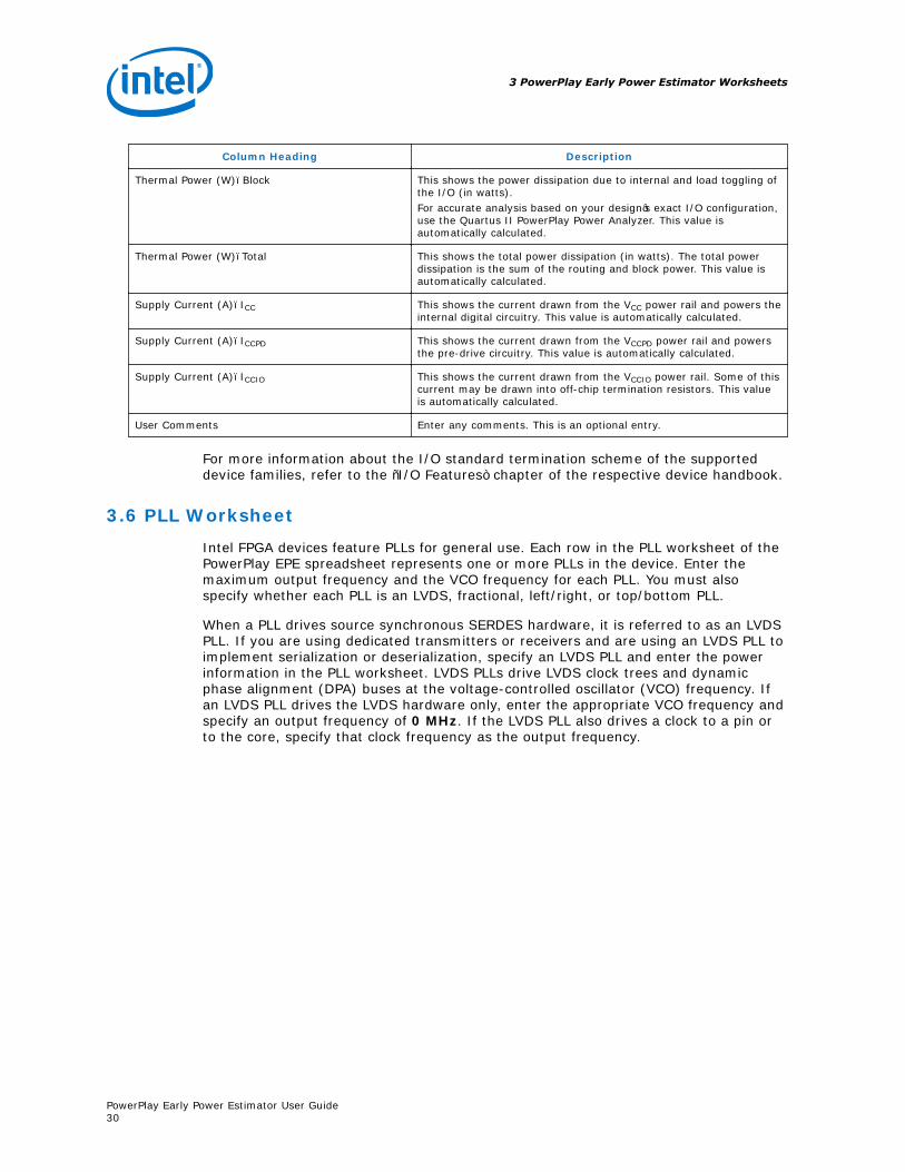
3.6 PLL Worksheet
Intel FPGA devices feature PLLs for general use. Each row in the PLL worksheet of thePowerPlay EPE spreadsheet represents one or more PLLs in the device. Enter themaximum output frequency and the VCO frequency for each PLL. You must alsospecify whether each PLL is an LVDS, fractional, left/right, or top/bottom PLL.
When a PLL drives source synchronous SERDES hardware, it is referred to as an LVDSPLL. If you are using dedicated transmitters or receivers and are using an LVDS PLL toimplement serialization or deserialization, specify an LVDS PLL and enter the powerinformation in the PLL worksheet. LVDS PLLs drive LVDS clock trees and dynamicphase alignment (DPA) buses at the voltage-controlled oscillator (VCO) frequency. Ifan LVDS PLL drives the LVDS hardware only, enter the appropriate VCO frequency andspecify an output frequency of 0 MHz. If the LVDS PLL also drives a clock to a pin orto the core, specify that clock frequency as the output frequency.
3 PowerPlay Early Power Estimator Worksheets
PowerPlay Early Power Estimator User Guide30
Figure 20. PLL Worksheet of the PowerPlay EPE Spreadsheet
Table 12. PLL Worksheet Information
Column Heading Description
Module Specify a name for the PLL in this column. This is an optional value.
PLL Type Select whether the PLL is a Fractional, Left/Right, Top/Bottom, or an LVDSPLL. This option is not applicable for all device families.
# PLL Blocks Enter the number of PLL blocks with the same specific output frequency and VCOfrequency combination.
# DPA Buses Enter the number of DPA buses in use. DPA is only available for LVDS PLLs. Thisoption is not applicable for all device families.
Output Freq (MHz) Enter the maximum output frequency of the PLL (in MHz). The maximum outputfrequency is reported in the Output Frequency column of the Quartus IICompilation Report. In the Compilation Report, select Fitter and clickResource Section. Select PLL Usage and click Output Frequency.
VCO Freq (MHz) Enter the internal VCO operating frequency for this module. The LVDS PLL drivesthe LVDS clock tree and DPA bus at this frequency. This frequency includes theVCO post scale counter.
Total Power (W) Shows the estimated combined power for VCCA and VCCD (in watts), based on themaximum output frequency and the VCO frequency you entered. This value isautomatically calculated.
User Comments Enter any comments. This is an optional entry.
For more information about the PLLs of the supported device families, refer to the“Clock Networks and PLLs“ chapter of the respective device handbook.
3.7 Clock Worksheet
Intel FPGA devices support global, regional, or periphery clock networks. ThePowerPlay EPE spreadsheet does not distinguish between global or regional clocksbecause the difference in power is not significant.
Each row in the Clock worksheet of the PowerPlay EPE spreadsheet represents a clocknetwork or a separate clock domain. Enter the following parameters for each designmodule:
3 PowerPlay Early Power Estimator Worksheets
PowerPlay Early Power Estimator User Guide31
• Clock frequency (in MHz)
• Total fanout for each clock network used
• Global clock enable percentage
• Local clock enable percentage
Figure 21. Clock Worksheet of the PowerPlay EPE Spreadsheet
Table 13. Clock Worksheet Information
Column Heading Description
Domain Specify a name for the clock network in this column. This is an optional value.
Clock Freq (MHz) Enter the frequency of the clock domain. This value is limited by the maximumfrequency specification for the device family.
Total Fanout Enter the total number of flipflops and RAM, DSP, and I/O blocks fed by thisclock. The number of resources driven by every global clock and regional clocksignal is reported in the Fan-out column of the Quartus II Compilation Report. Inthe Compilation Report, select Fitter and click Resources Section. SelectGlobal and Other Fast Signals and click Fan-out.
Global Enable % Enter the average percentage of time that the entire clock tree is enabled. Eachglobal clock buffer has an enable signal that you can use to dynamically shutdown the entire clock tree.
Local Enable % Enter the average percentage of time that clock enable is high for destinationflipflops.Local clock enables for flipflops in ALMs are promoted to LAB-wide signals. Whena given flipflop is disabled, the LAB-wide is clock disabled, cutting clock powerand the power for down-stream logic. This worksheet models only the impact onclock tree power.
Total Power (W) This is the total power dissipation due to clock distribution (in watts). This valueis automatically calculated.
User Comments Enter any comments. This is an optional entry.
For more information about the clock networks of the supported device families, referto the “Clock Networks and PLLs” chapter of the respective device handbook.
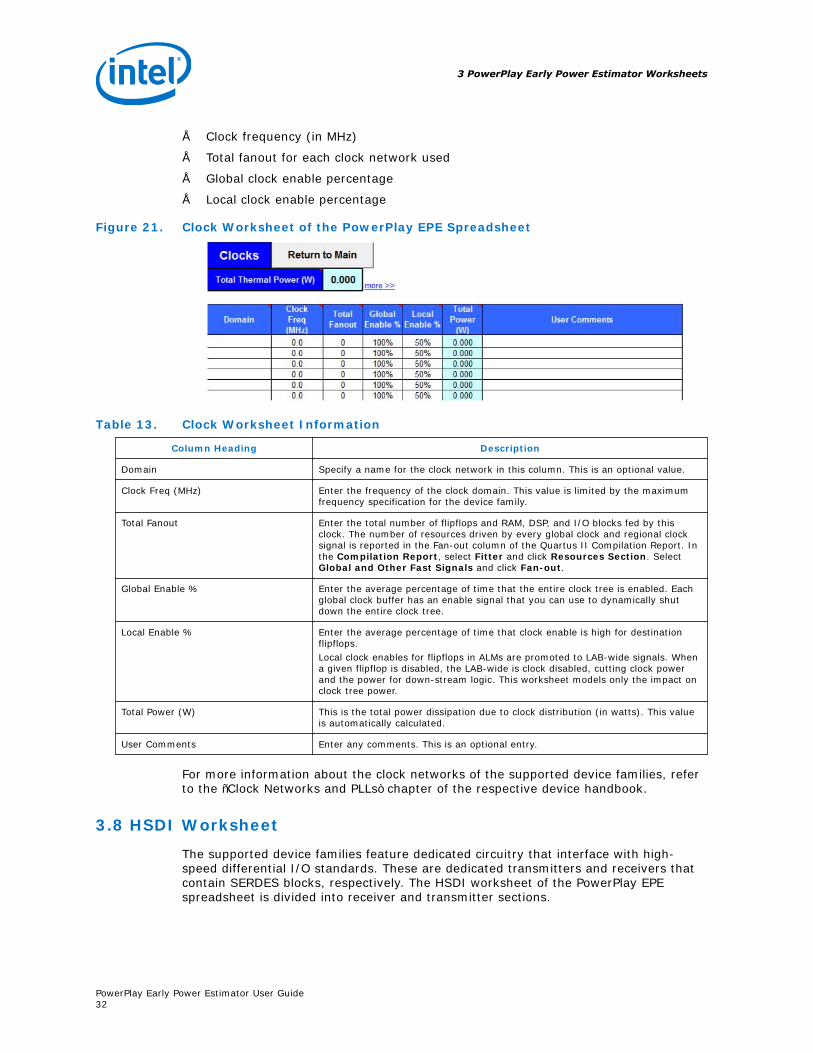
3.8 HSDI Worksheet
The supported device families feature dedicated circuitry that interface with high-speed differential I/O standards. These are dedicated transmitters and receivers thatcontain SERDES blocks, respectively. The HSDI worksheet of the PowerPlay EPEspreadsheet is divided into receiver and transmitter sections.
3 PowerPlay Early Power Estimator Worksheets
PowerPlay Early Power Estimator User Guide32
The power calculated in the HSDI worksheet of the PowerPlay EPE spreadsheet onlyapplies to the transmitter serializer block or the receiver deserializer block. Thetransmitter and receiver are implemented using the ALTLVDS megafunction. The I/Obuffer power is calculated in the I/O worksheet and the PLL power is calculated in thePLL worksheet.
Each row in the HSDI worksheet of the PowerPlay EPE spreadsheet represents aseparate receiver or transmitter domain. Specify the following parameters fortransmitter and receiver domains:
• Data rate (in Mbps)
• Number of channels
• Serialization factor in the transmitter domain
• Deserialization factor in the receiver domain
• Toggle percentage
The receiver power is the same whether or not you use the DPA circuitry.
Figure 22. HSDI Worksheet of the PowerPlay EPE Spreadsheet
3 PowerPlay Early Power Estimator Worksheets
PowerPlay Early Power Estimator User Guide33
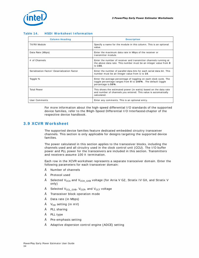
Table 14. HSDI Worksheet Information
Column Heading Description
TX/RX Module Specify a name for the module in this column. This is an optionalvalue.
Data Rate (Mbps) Enter the maximum data rate in Mbps of the receiver ortransmitter module.
# of Channels Enter the number of receiver and transmitter channels running atthe above data rate. This number must be an integer value from 0to 156.
Serialization Factor/ Deserialization Factor Enter the number of parallel data bits for each serial data bit. Thisnumber must be an integer value from 1 to 10.
Toggle % Enter the average percentage of toggling on each clock cycle. Thetoggle percentage ranges from 0 to 100%. The default togglepercentage is 50%.
Total Power This shows the estimated power (in watts) based on the data rateand number of channels you entered. This value is automaticallycalculated.
User Comments Enter any comments. This is an optional entry.
For more information about the high-speed differential I/O standards of the supporteddevice families, refer to the “High-Speed Differential I/O Interfaces” chapter of therespective device handbook.
3.9 XCVR Worksheet
The supported device families feature dedicated embedded circuitry transceiverchannels. This section is only applicable for designs targeting the supported devicefamilies.
The power calculated in this section applies to the transceiver blocks, including thechannels used and all circuitry used in the clock control unit (CCU). The I/O bufferpower and PLL power for the transceivers are included in this section. Transmittersand receivers assume 100 Ω termination.
Each row in the XCVR worksheet represents a separate transceiver domain. Enter thefollowing parameters for each transceiver domain:
• Number of channels
• Protocol used
• Selected VCCA and VCCH_GXB voltage (for Arria V GZ, Stratix IV GX, and Stratix Vonly)
• Selected VCCL_GXB, VCCR, and VCCT voltage
• Transceiver block operation mode
• Data rate (in Mbps)
• VOD setting (in mV)
• PLL sharing
• PLL type
• Pre-emphasis setting
• Adaptive dispersion control engine (ADCE) setting
3 PowerPlay Early Power Estimator Worksheets
PowerPlay Early Power Estimator User Guide34
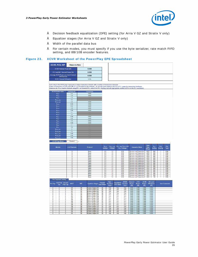
• Decision feedback equalization (DFE) setting (for Arria V GZ and Stratix V only)
• Equalizer stages (for Arria V GZ and Stratix V only)
• Width of the parallel data bus
• For certain modes, you must specify if you use the byte serializer, rate match FIFOsetting, and 8B/10B encoder features.
Figure 23. XCVR Worksheet of the PowerPlay EPE Spreadsheet
3 PowerPlay Early Power Estimator Worksheets
PowerPlay Early Power Estimator User Guide35
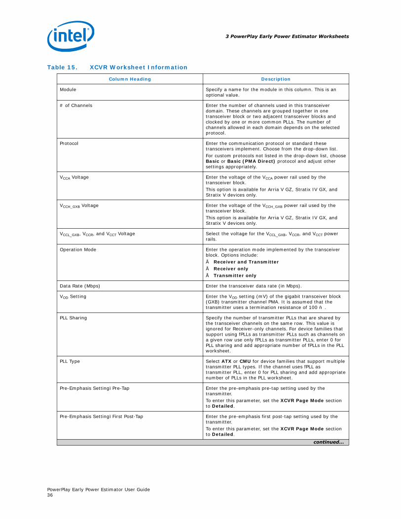
Table 15. XCVR Worksheet Information
Column Heading Description
Module Specify a name for the module in this column. This is anoptional value.
# of Channels Enter the number of channels used in this transceiverdomain. These channels are grouped together in onetransceiver block or two adjacent transceiver blocks andclocked by one or more common PLLs. The number ofchannels allowed in each domain depends on the selectedprotocol.
Protocol Enter the communication protocol or standard thesetransceivers implement. Choose from the drop-down list.For custom protocols not listed in the drop-down list, chooseBasic or Basic (PMA Direct) protocol and adjust othersettings appropriately.
VCCA Voltage Enter the voltage of the VCCA power rail used by thetransceiver block.This option is available for Arria V GZ, Stratix IV GX, andStratix V devices only.
VCCH_GXB Voltage Enter the voltage of the VCCH_GXB power rail used by thetransceiver block.This option is available for Arria V GZ, Stratix IV GX, andStratix V devices only.
VCCL_GXB, VCCR, and VCCT Voltage Select the voltage for the VCCL_GXB, VCCR, and VCCT powerrails.
Operation Mode Enter the operation mode implemented by the transceiverblock. Options include:• Receiver and Transmitter• Receiver only• Transmitter only
Data Rate (Mbps) Enter the transceiver data rate (in Mbps).
VOD Setting Enter the VOD setting (mV) of the gigabit transceiver block(GXB) transmitter channel PMA. It is assumed that thetransmitter uses a termination resistance of 100 Ω .
PLL Sharing Specify the number of transmitter PLLs that are shared bythe transceiver channels on the same row. This value isignored for Receiver-only channels. For device families thatsupport using fPLLs as transmitter PLLs such as channels ona given row use only fPLLs as transmitter PLLs, enter 0 forPLL sharing and add appropriate number of fPLLs in the PLLworksheet.
PLL Type Select ATX or CMU for device families that support multipletransmitter PLL types. If the channel uses fPLL astransmitter PLL, enter 0 for PLL sharing and add appropriatenumber of PLLs in the PLL worksheet.
Pre-Emphasis Setting–Pre-Tap Enter the pre-emphasis pre-tap setting used by thetransmitter.To enter this parameter, set the XCVR Page Mode sectionto Detailed.
Pre-Emphasis Setting–First Post-Tap Enter the pre-emphasis first post-tap setting used by thetransmitter.To enter this parameter, set the XCVR Page Mode sectionto Detailed.
continued...
3 PowerPlay Early Power Estimator Worksheets
PowerPlay Early Power Estimator User Guide36

Column Heading Description
Pre-Emphasis Setting–Second Post-Tap Enter the pre-emphasis second post-tap setting used by thetransmitter.To enter this parameter, set the XCVR Page Mode sectionto Detailed.
ADCE Enter whether the ADCE is turned On or Off.To enter this parameter, set the XCVR Page Mode sectionto Detailed.
DFE Specify DFE mode as Manual or Triggered Adaptionwhen DFE is used. The DFE is turned Off by default.To enter this parameter, set the XCVR Page Mode sectionto Detailed.
Equalizer stages Select All stages Enabled or Bypass Stages 234. Bypassequalizer stages 2, 3, and 4 reduce power consumption ofthe transceiver channels.
Parallel Data Width Enter the width of the parallel data bus going into each GXBtransmitter channel PCS and coming out of each GXBreceiver channel PCS.To enter this parameter, set the XCVR Page Mode sectionto Detailed.
Byte Serializer Used Enter whether or not the byte SERDES is used. If the byteserializer is used, the transceiver is in double-width mode. Ifit is not used, the transceiver is in single-width mode.To enter this parameter, set the XCVR Page Mode sectionto Detailed.
Rate Match FIFO Used Enter whether or not the rate matching FIFO is used.To enter this parameter, set the XCVR Page Mode sectionto Detailed.
8B10B Encoder Used Enter whether or not 8B/10B encoder/decoder is used.To enter this parameter, set the XCVR Page Mode sectionto Detailed.
Channel Power (W) This shows the total power of the GXB transmitter channelPMA and GXB receiver channel PMA blocks for all channels(in watts). This value is automatically calculated.
CCU Power (W) This shows the total power of the GXB PLLs and controlcircuitry for all channels (in watts). This value isautomatically calculated.
XCVR Power (W) This shows the sum of the channel power and CCU power(in watts). This value is automatically calculated.
PCS/HIP Power (W) This shows the total power of the GXB transmitter channelPCS, GXB receiver channel PCS, and PCIe hard IP blocks forall channels (in watts). This value is automaticallycalculated.
User Comments Enter any comments. This is an optional entry.
Values of some settings in the XCVR worksheet are restricted for one of the followingreasons:
• The setting value is restricted due to the selections made for other settings.
• Changing the setting would not have a significant impact on power, given theselected values of other settings.
For more information about the transceiver architecture of the supported devicefamilies, refer to the “Transceiver Architecture” chapter in the respective devicehandbook.
3 PowerPlay Early Power Estimator Worksheets
PowerPlay Early Power Estimator User Guide37
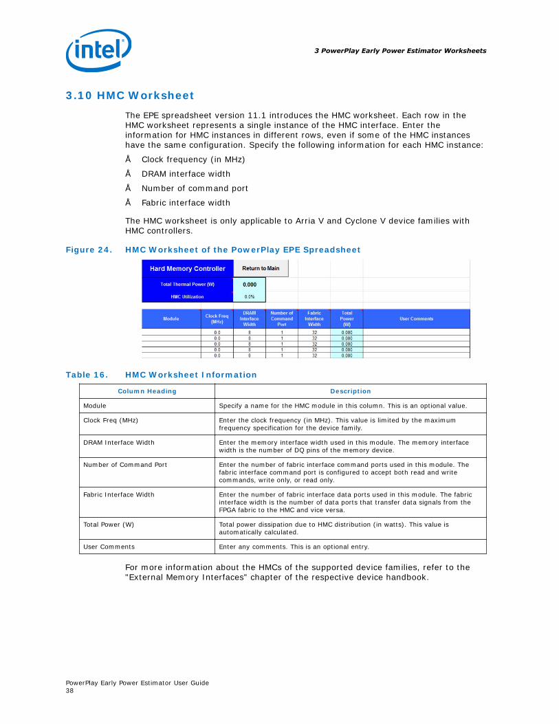
3.10 HMC Worksheet
The EPE spreadsheet version 11.1 introduces the HMC worksheet. Each row in theHMC worksheet represents a single instance of the HMC interface. Enter theinformation for HMC instances in different rows, even if some of the HMC instanceshave the same configuration. Specify the following information for each HMC instance:
• Clock frequency (in MHz)
• DRAM interface width
• Number of command port
• Fabric interface width
The HMC worksheet is only applicable to Arria V and Cyclone V device families withHMC controllers.
Figure 24. HMC Worksheet of the PowerPlay EPE Spreadsheet
Table 16. HMC Worksheet Information
Column Heading Description
Module Specify a name for the HMC module in this column. This is an optional value.
Clock Freq (MHz) Enter the clock frequency (in MHz). This value is limited by the maximumfrequency specification for the device family.
DRAM Interface Width Enter the memory interface width used in this module. The memory interfacewidth is the number of DQ pins of the memory device.
Number of Command Port Enter the number of fabric interface command ports used in this module. Thefabric interface command port is configured to accept both read and writecommands, write only, or read only.
Fabric Interface Width Enter the number of fabric interface data ports used in this module. The fabricinterface width is the number of data ports that transfer data signals from theFPGA fabric to the HMC and vice versa.
Total Power (W) Total power dissipation due to HMC distribution (in watts). This value isautomatically calculated.
User Comments Enter any comments. This is an optional entry.
For more information about the HMCs of the supported device families, refer to the"External Memory Interfaces" chapter of the respective device handbook.
3 PowerPlay Early Power Estimator Worksheets
PowerPlay Early Power Estimator User Guide38
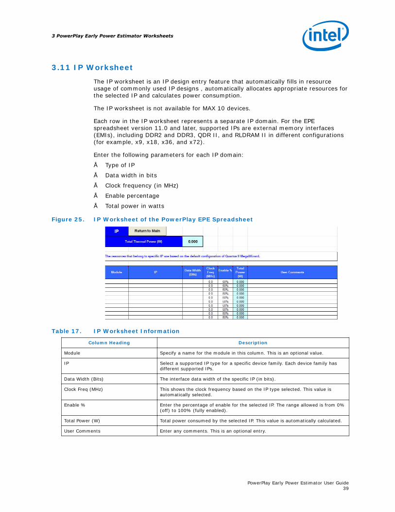
3.11 IP Worksheet
The IP worksheet is an IP design entry feature that automatically fills in resourceusage of commonly used IP designs , automatically allocates appropriate resources forthe selected IP and calculates power consumption.
The IP worksheet is not available for MAX 10 devices.
Each row in the IP worksheet represents a separate IP domain. For the EPEspreadsheet version 11.0 and later, supported IPs are external memory interfaces(EMIs), including DDR2 and DDR3, QDR II, and RLDRAM II in different configurations(for example, x9, x18, x36, and x72).
Enter the following parameters for each IP domain:
• Type of IP
• Data width in bits
• Clock frequency (in MHz)
• Enable percentage
• Total power in watts
Figure 25. IP Worksheet of the PowerPlay EPE Spreadsheet
Table 17. IP Worksheet Information
Column Heading Description
Module Specify a name for the module in this column. This is an optional value.
IP Select a supported IP type for a specific device family. Each device family hasdifferent supported IPs.
Data Width (Bits) The interface data width of the specific IP (in bits).
Clock Freq (MHz) This shows the clock frequency based on the IP type selected. This value isautomatically selected.
Enable % Enter the percentage of enable for the selected IP. The range allowed is from 0%(off) to 100% (fully enabled).
Total Power (W) Total power consumed by the selected IP. This value is automatically calculated.
User Comments Enter any comments. This is an optional entry.
3 PowerPlay Early Power Estimator Worksheets
PowerPlay Early Power Estimator User Guide39
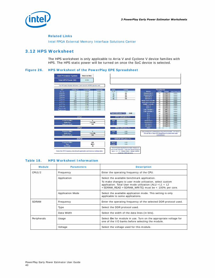
Related Links
Intel FPGA External Memory Interface Solutions Center
3.12 HPS Worksheet
The HPS worksheet is only applicable to Arria V and Cyclone V device families withHPS. The HPS static power will be turned on once the SoC device is selected.
Figure 26. HPS Worksheet of the PowerPlay EPE Spreadsheet
Table 18. HPS Worksheet Information
Module Parameters Description
CPU1/2 Frequency Enter the operating frequency of the CPU.
Application Select the available benchmark application.To make changes to user mode utilization, select customapplication. Total User mode utilization (ALU +L1 + L2+SDRAM_READ +SDRAM_WRITE) must be < 100% per core.
Application Mode Select the available application mode. This setting is onlyapplicable to some applications.
SDRAM Frequency Enter the operating frequency of the selected DDR protocol used.
Type Select the DDR protocol used.
Data Width Select the width of the data lines (in bits).
Peripherals Usage Select On for module in use. Turn on the appropriate voltage forone of the I/O banks before selecting the module.
Voltage Select the voltage used for this module.
3 PowerPlay Early Power Estimator Worksheets
PowerPlay Early Power Estimator User Guide40
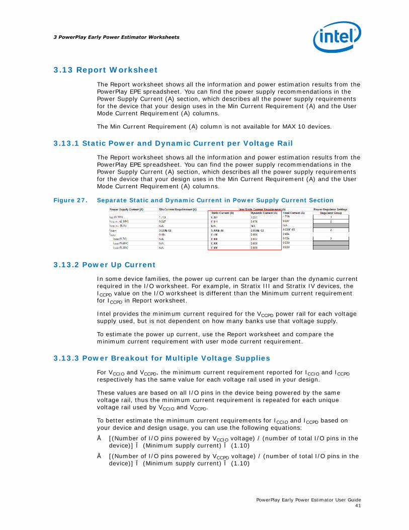
3.13 Report Worksheet
The Report worksheet shows all the information and power estimation results from thePowerPlay EPE spreadsheet. You can find the power supply recommendations in thePower Supply Current (A) section, which describes all the power supply requirementsfor the device that your design uses in the Min Current Requirement (A) and the UserMode Current Requirement (A) columns.
The Min Current Requirement (A) column is not available for MAX 10 devices.
3.13.1 Static Power and Dynamic Current per Voltage Rail
The Report worksheet shows all the information and power estimation results from thePowerPlay EPE spreadsheet. You can find the power supply recommendations in thePower Supply Current (A) section, which describes all the power supply requirementsfor the device that your design uses in the Min Current Requirement (A) and the UserMode Current Requirement (A) columns.
Figure 27. Separate Static and Dynamic Current in Power Supply Current Section
3.13.2 Power Up Current
In some device families, the power up current can be larger than the dynamic currentrequired in the I/O worksheet. For example, in Stratix III and Stratix IV devices, theICCPD value on the I/O worksheet is different than the Minimum current requirementfor ICCPD in Report worksheet.
Intel provides the minimum current required for the VCCPD power rail for each voltagesupply used, but is not dependent on how many banks use that voltage supply.
To estimate the power up current, use the Report worksheet and compare theminimum current requirement with user mode current requirement.
3.13.3 Power Breakout for Multiple Voltage Supplies
For VCCIO and VCCPD, the minimum current requirement reported for ICCIO and ICCPDrespectively has the same value for each voltage rail used in your design.
These values are based on all I/O pins in the device being powered by the samevoltage rail, thus the minimum current requirement is repeated for each uniquevoltage rail used by VCCIO and VCCPD.
To better estimate the minimum current requirements for ICCIO and ICCPD based onyour device and design usage, you can use the following equations:
• [(Number of I/O pins powered by VCCIO voltage) / (number of total I/O pins in thedevice)] × (Minimum supply current) × (1.10)
• [(Number of I/O pins powered by VCCPD voltage) / (number of total I/O pins in thedevice)] × (Minimum supply current) × (1.10)
3 PowerPlay Early Power Estimator Worksheets
PowerPlay Early Power Estimator User Guide41
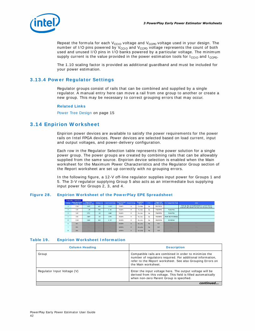
Repeat the formula for each VCCIO voltage and VCCPD voltage used in your design. Thenumber of I/O pins powered by VCCIO and VCCPD voltage represents the count of bothused and unused I/O pins in I/O banks powered by a particular voltage. The minimumsupply current is the value provided in the power estimation tools for ICCIO and ICCPD.
The 1.10 scaling factor is provided as additional guardband and must be included foryour power estimation.
3.13.4 Power Regulator Settings
Regulator groups consist of rails that can be combined and supplied by a singleregulator. A manual entry here can move a rail from one group to another or create anew group. This may be necessary to correct grouping errors that may occur.
Related Links
Power Tree Design on page 15
3.14 Enpirion Worksheet
Enpirion power devices are available to satisfy the power requirements for the powerrails on Intel FPGA devices. Power devices are selected based on load current, inputand output voltages, and power-delivery configuration.
Each row in the Regulator Selection table represents the power solution for a singlepower group. The power groups are created by combining rails that can be allowablysupplied from the same source. Enpirion device selection is enabled when the Mainworksheet for the Maximum Power Characteristics and the Regulator Group section ofthe Report worksheet are set up correctly with no grouping errors.
In the following figure, a 12-V off-line regulator supplies input power for Groups 1 and5. The 3-V regulator supplying Group 5 also acts as an intermediate bus supplyinginput power for Groups 2, 3, and 4.
Figure 28. Enpirion Worksheet of the PowerPlay EPE Spreadsheet
Table 19. Enpirion Worksheet Information
Column Heading Description
Group Compatible rails are combined in order to minimize thenumber of regulators required. For additional information,refer to the Report worksheet. See also Grouping Errors onthe Main worksheet.
Regulator Input Voltage (V) Enter the input voltage here. The output voltage will bederived from this voltage. This field is filled automaticallywhen non-zero Parent Group is specified.
continued...
3 PowerPlay Early Power Estimator Worksheets
PowerPlay Early Power Estimator User Guide42

Column Heading Description
Load Current Margin Margin can be added to account for component variability. Itis recommended to retain the default 30% to assure thethermal capability of the solution over the full range ofdevice variation and operating conditions. However, incertain cases when characteristics and conditions are fullydefined, reducing the margin may lead to a more cost-effective solution. Exercise caution when changing thesevalues.
Parent Group If one of the group voltages is to be used as anintermediate bus voltage, enter the group number here.
Regulator Type In some cases, a linear regulator (LDO) may be a goodchoice to supply one of the group voltages. The efficiency ofan LDO is the ratio of output voltage to input voltage. In thefigure, Group 2 can be efficiently supplied by an LDO. Ifdesired, select Linear in the row for Group 2.
POK Select Yes to select a regulator with a Power OK (POK)output to assist with sequencing.
Suggested Enpirion Part Suggested Enpirion part is automatically populated with thepart number of the device that most closely matches theLoad Current (A), Regulator Type and POK selections.The dropdown can be used to optionally select devices withequivalent or higher current capabilities.
Pin Compatible Parts Pin compatible parts are devices with equivalent or highercurrent capabilities that can be placed on the same PCBfootprint as the Suggested Enpirion Part. Additionalcomponents or changes to component values may berequired when using a pin compatible part.
Related Links
• Power Tree Design on page 15
• Report Worksheet on page 41
3 PowerPlay Early Power Estimator Worksheets
PowerPlay Early Power Estimator User Guide43
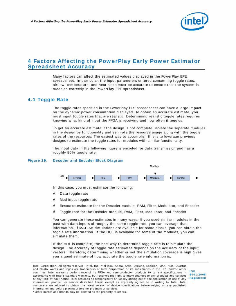
4 Factors Affecting the PowerPlay Early Power EstimatorSpreadsheet Accuracy
Many factors can affect the estimated values displayed in the PowerPlay EPEspreadsheet. In particular, the input parameters entered concerning toggle rates,airflow, temperature, and heat sinks must be accurate to ensure that the system ismodeled correctly in the PowerPlay EPE spreadsheet.
4.1 Toggle Rate
The toggle rates specified in the PowerPlay EPE spreadsheet can have a large impacton the dynamic power consumption displayed. To obtain an accurate estimate, youmust input toggle rates that are realistic. Determining realistic toggle rates requiresknowing what kind of input the FPGA is receiving and how often it toggles.
To get an accurate estimate if the design is not complete, isolate the separate modulesin the design by functionality and estimate the resource usage along with the togglerates of the resources. The easiest way to accomplish this is to leverage previousdesigns to estimate the toggle rates for modules with similar functionality.
The input data in the following figure is encoded for data transmission and has aroughly 50% toggle rate.
Figure 29. Decoder and Encoder Block Diagram
Decoder RAM Filter Modulator Encoder
Mod Input
Data
In this case, you must estimate the following:
• Data toggle rate
• Mod input toggle rate
• Resource estimate for the Decoder module, RAM, Filter, Modulator, and Encoder
• Toggle rate for the Decoder module, RAM, Filter, Modulator, and Encoder
You can generate these estimates in many ways. If you used similar modules in thepast with data inputs of roughly the same toggle rate, you can leverage thatinformation. If MATLAB simulations are available for some blocks, you can obtain thetoggle rate information. If the HDL is available for some of the modules, you cansimulate them.
If the HDL is complete, the best way to determine toggle rate is to simulate thedesign. The accuracy of toggle rate estimates depends on the accuracy of the inputvectors. Therefore, determining whether or not the simulation coverage is high givesyou a good estimate of how accurate the toggle rate information is.
4 Factors Affecting the PowerPlay Early Power Estimator Spreadsheet Accuracy
Intel Corporation. All rights reserved. Intel, the Intel logo, Altera, Arria, Cyclone, Enpirion, MAX, Nios, Quartusand Stratix words and logos are trademarks of Intel Corporation or its subsidiaries in the U.S. and/or othercountries. Intel warrants performance of its FPGA and semiconductor products to current specifications inaccordance with Intel's standard warranty, but reserves the right to make changes to any products and servicesat any time without notice. Intel assumes no responsibility or liability arising out of the application or use of anyinformation, product, or service described herein except as expressly agreed to in writing by Intel. Intelcustomers are advised to obtain the latest version of device specifications before relying on any publishedinformation and before placing orders for products or services.*Other names and brands may be claimed as the property of others.
ISO9001:2008Registered
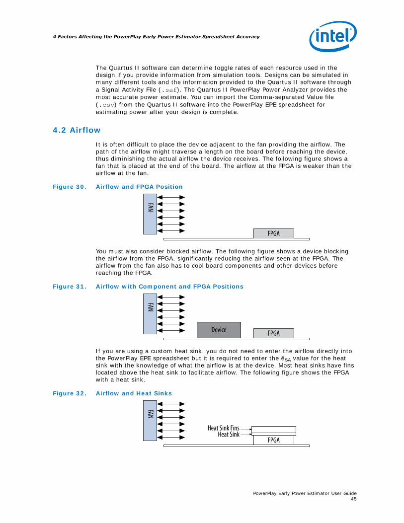
The Quartus II software can determine toggle rates of each resource used in thedesign if you provide information from simulation tools. Designs can be simulated inmany different tools and the information provided to the Quartus II software througha Signal Activity File (.saf). The Quartus II PowerPlay Power Analyzer provides themost accurate power estimate. You can import the Comma-separated Value file(.csv) from the Quartus II software into the PowerPlay EPE spreadsheet forestimating power after your design is complete.
4.2 Airflow
It is often difficult to place the device adjacent to the fan providing the airflow. Thepath of the airflow might traverse a length on the board before reaching the device,thus diminishing the actual airflow the device receives. The following figure shows afan that is placed at the end of the board. The airflow at the FPGA is weaker than theairflow at the fan.
Figure 30. Airflow and FPGA Position
FAN
FPGA
You must also consider blocked airflow. The following figure shows a device blockingthe airflow from the FPGA, significantly reducing the airflow seen at the FPGA. Theairflow from the fan also has to cool board components and other devices beforereaching the FPGA.
Figure 31. Airflow with Component and FPGA Positions
FAN
FPGADevice
If you are using a custom heat sink, you do not need to enter the airflow directly intothe PowerPlay EPE spreadsheet but it is required to enter the θSA value for the heatsink with the knowledge of what the airflow is at the device. Most heat sinks have finslocated above the heat sink to facilitate airflow. The following figure shows the FPGAwith a heat sink.
Figure 32. Airflow and Heat Sinks
FAN
FPGA
Heat Sink FinsHeat Sink
4 Factors Affecting the PowerPlay Early Power Estimator Spreadsheet Accuracy
PowerPlay Early Power Estimator User Guide45
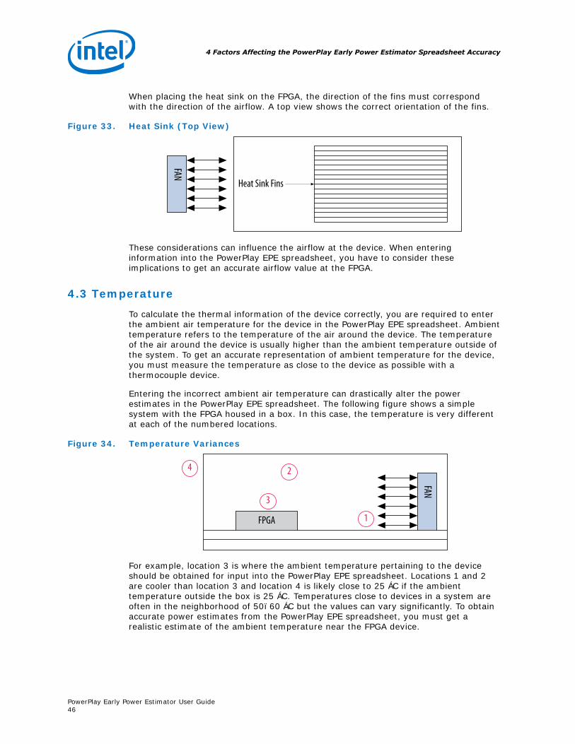
When placing the heat sink on the FPGA, the direction of the fins must correspondwith the direction of the airflow. A top view shows the correct orientation of the fins.
Figure 33. Heat Sink (Top View)
FAN
Heat Sink Fins
These considerations can influence the airflow at the device. When enteringinformation into the PowerPlay EPE spreadsheet, you have to consider theseimplications to get an accurate airflow value at the FPGA.
4.3 Temperature
To calculate the thermal information of the device correctly, you are required to enterthe ambient air temperature for the device in the PowerPlay EPE spreadsheet. Ambienttemperature refers to the temperature of the air around the device. The temperatureof the air around the device is usually higher than the ambient temperature outside ofthe system. To get an accurate representation of ambient temperature for the device,you must measure the temperature as close to the device as possible with athermocouple device.
Entering the incorrect ambient air temperature can drastically alter the powerestimates in the PowerPlay EPE spreadsheet. The following figure shows a simplesystem with the FPGA housed in a box. In this case, the temperature is very differentat each of the numbered locations.
Figure 34. Temperature Variances
FAN
1
2
3
4
FPGA
For example, location 3 is where the ambient temperature pertaining to the deviceshould be obtained for input into the PowerPlay EPE spreadsheet. Locations 1 and 2are cooler than location 3 and location 4 is likely close to 25 °C if the ambienttemperature outside the box is 25 °C. Temperatures close to devices in a system areoften in the neighborhood of 50–60 °C but the values can vary significantly. To obtainaccurate power estimates from the PowerPlay EPE spreadsheet, you must get arealistic estimate of the ambient temperature near the FPGA device.
4 Factors Affecting the PowerPlay Early Power Estimator Spreadsheet Accuracy
PowerPlay Early Power Estimator User Guide46
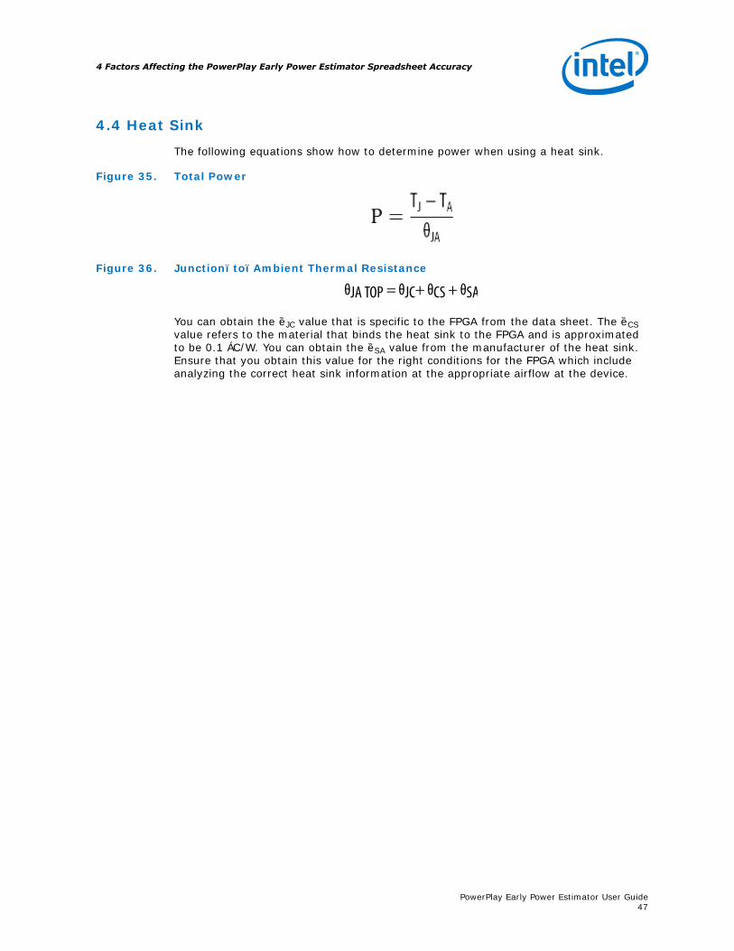
4.4 Heat Sink
The following equations show how to determine power when using a heat sink.
Figure 35. Total Power
Figure 36. Junction–to–Ambient Thermal Resistance
θJA TOP = θJC+ θCS + θSA
You can obtain the θJC value that is specific to the FPGA from the data sheet. The θCSvalue refers to the material that binds the heat sink to the FPGA and is approximatedto be 0.1 °C/W. You can obtain the θSA value from the manufacturer of the heat sink.Ensure that you obtain this value for the right conditions for the FPGA which includeanalyzing the correct heat sink information at the appropriate airflow at the device.
4 Factors Affecting the PowerPlay Early Power Estimator Spreadsheet Accuracy
PowerPlay Early Power Estimator User Guide47
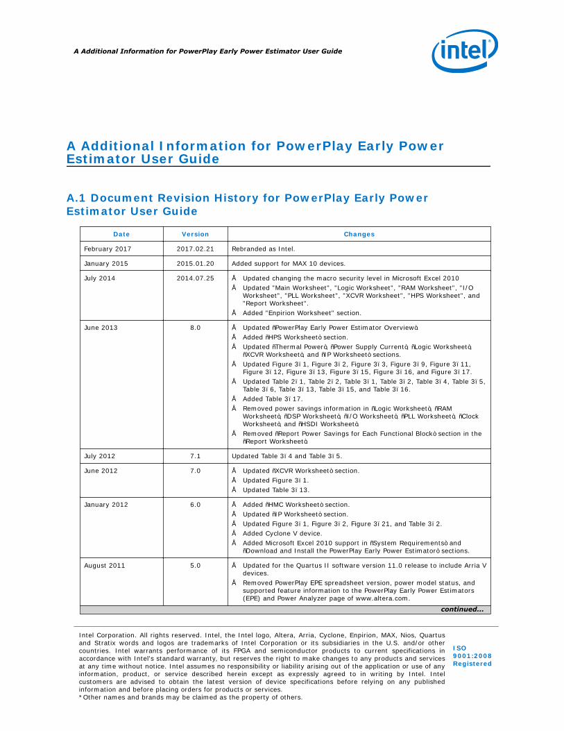
A Additional Information for PowerPlay Early PowerEstimator User Guide
A.1 Document Revision History for PowerPlay Early PowerEstimator User Guide
Date Version Changes
February 2017 2017.02.21 Rebranded as Intel.
January 2015 2015.01.20 Added support for MAX 10 devices.
July 2014 2014.07.25 • Updated changing the macro security level in Microsoft Excel 2010• Updated "Main Worksheet", "Logic Worksheet", "RAM Worksheet", "I/O
Worksheet", "PLL Worksheet", "XCVR Worksheet", "HPS Worksheet", and"Report Worksheet".
• Added "Enpirion Worksheet" section.
June 2013 8.0 • Updated “PowerPlay Early Power Estimator Overview”.• Added “HPS Worksheet” section.• Updated “Thermal Power”, “Power Supply Current”, “Logic Worksheet”,
“XCVR Worksheet”, and “IP Worksheet” sections.• Updated Figure 3–1, Figure 3–2, Figure 3–3, Figure 3–9, Figure 3–11,
Figure 3–12, Figure 3–13, Figure 3–15, Figure 3–16, and Figure 3–17.• Updated Table 2–1, Table 2–2, Table 3–1, Table 3–2, Table 3–4, Table 3–5,
Table 3–6, Table 3–13, Table 3–15, and Table 3–16.• Added Table 3–17.• Removed power savings information in “Logic Worksheet”, “RAM
Worksheet”, “DSP Worksheet”, “I/O Worksheet”, “PLL Worksheet”, “ClockWorksheet”, and “HSDI Worksheet”.
• Removed “Report Power Savings for Each Functional Block” section in the“Report Worksheet”.
July 2012 7.1 Updated Table 3–4 and Table 3–5.
June 2012 7.0 • Updated “XCVR Worksheet” section.• Updated Figure 3–1.• Updated Table 3–13.
January 2012 6.0 • Added “HMC Worksheet” section.• Updated “IP Worksheet” section.• Updated Figure 3–1, Figure 3–2, Figure 3–21, and Table 3–2.• Added Cyclone V device.• Added Microsoft Excel 2010 support in “System Requirements” and
“Download and Install the PowerPlay Early Power Estimator” sections.
August 2011 5.0 • Updated for the Quartus II software version 11.0 release to include Arria Vdevices.
• Removed PowerPlay EPE spreadsheet version, power model status, andsupported feature information to the PowerPlay Early Power Estimators(EPE) and Power Analyzer page of www.altera.com.
continued...
A Additional Information for PowerPlay Early Power Estimator User Guide
Intel Corporation. All rights reserved. Intel, the Intel logo, Altera, Arria, Cyclone, Enpirion, MAX, Nios, Quartusand Stratix words and logos are trademarks of Intel Corporation or its subsidiaries in the U.S. and/or othercountries. Intel warrants performance of its FPGA and semiconductor products to current specifications inaccordance with Intel's standard warranty, but reserves the right to make changes to any products and servicesat any time without notice. Intel assumes no responsibility or liability arising out of the application or use of anyinformation, product, or service described herein except as expressly agreed to in writing by Intel. Intelcustomers are advised to obtain the latest version of device specifications before relying on any publishedinformation and before placing orders for products or services.*Other names and brands may be claimed as the property of others.
ISO9001:2008Registered
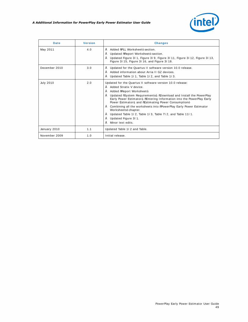
Date Version Changes
May 2011 4.0 • Added “PLL Worksheet” section.• Updated “Report Worksheet” section.• Updated Figure 3–1, Figure 3–9, Figure 3–11, Figure 3–12, Figure 3–13,
Figure 3–15, Figure 3–16, and Figure 3–18.
December 2010 3.0 • Updated for the Quartus II software version 10.0 release.• Added information about Arria II GZ devices.• Updated Table 1–1, Table 1–2, and Table 1–3.
July 2010 2.0 Updated for the Quartus II software version 10.0 release:• Added Stratix V device.• Added “Report Worksheet”.• Updated “System Requirements”, “Download and Install the PowerPlay
Early Power Estimator”, “Entering Information into the PowerPlay EarlyPower Estimator”, and “Estimating Power Consumption”
• Combining all the worksheets into “PowerPlay Early Power EstimatorWorksheets” chapter.
• Updated Table 1–2, Table 1–3, Table 7–2, and Table 11–1.• Updated Figure 3–1.• Minor text edits.
January 2010 1.1 Updated Table 1–2 and Table.
November 2009 1.0 Initial release.
A Additional Information for PowerPlay Early Power Estimator User Guide
PowerPlay Early Power Estimator User Guide49