Embed Size (px)
Citation preview

Mixed-Signal Computer-Aided Deisgn Laboratory
PowerSynth User Manual
April 24, 2019
Energy-Efficient Electronics and Design Automation Laboratory

Contents
1 Introduction 3
1.1 Executive Summary . . . . . . . . . . . . . . . . . . . . . . . . . . . . . . . . . . . . 31.2 Organization . . . . . . . . . . . . . . . . . . . . . . . . . . . . . . . . . . . . . . . . 31.3 PowerSynth Overview . . . . . . . . . . . . . . . . . . . . . . . . . . . . . . . . . . . 3
1.3.1 Constraint-Aware Layout Engine . . . . . . . . . . . . . . . . . . . . . . . . . 5
2 Using PowerSynth 8
2.1 Installing PowerSynth . . . . . . . . . . . . . . . . . . . . . . . . . . . . . . . . . . . 82.2 Creating a New Project in PowerSynth . . . . . . . . . . . . . . . . . . . . . . . . . . 8
2.2.1 User Interface . . . . . . . . . . . . . . . . . . . . . . . . . . . . . . . . . . . . 82.2.2 Symbolic Layout File . . . . . . . . . . . . . . . . . . . . . . . . . . . . . . . . 82.2.3 Create a New Project . . . . . . . . . . . . . . . . . . . . . . . . . . . . . . . 10
2.3 De�ning the Module and Components . . . . . . . . . . . . . . . . . . . . . . . . . . 102.3.1 Module Stack . . . . . . . . . . . . . . . . . . . . . . . . . . . . . . . . . . . . 102.3.2 Layer Stack File . . . . . . . . . . . . . . . . . . . . . . . . . . . . . . . . . . 112.3.3 Component Selection . . . . . . . . . . . . . . . . . . . . . . . . . . . . . . . . 122.3.4 Device and Lead Selection . . . . . . . . . . . . . . . . . . . . . . . . . . . . . 142.3.5 Assigning Devices and Leads . . . . . . . . . . . . . . . . . . . . . . . . . . . 152.3.6 Assigning Virtual Wire Connections . . . . . . . . . . . . . . . . . . . . . . . 16
2.4 De�ning Correlations and Constraints . . . . . . . . . . . . . . . . . . . . . . . . . . 172.4.1 Design Variable Correlation . . . . . . . . . . . . . . . . . . . . . . . . . . . . 172.4.2 Constraint Creation . . . . . . . . . . . . . . . . . . . . . . . . . . . . . . . . 17
2.5 Design Performance Identi�cation . . . . . . . . . . . . . . . . . . . . . . . . . . . . . 182.5.1 Thermal Measurement . . . . . . . . . . . . . . . . . . . . . . . . . . . . . . . 182.5.2 ARL ParaPower Thermal Analysis . . . . . . . . . . . . . . . . . . . . . . . . 182.5.3 Electrical Measurement . . . . . . . . . . . . . . . . . . . . . . . . . . . . . . 212.5.4 Inductance and Resistance Measurement . . . . . . . . . . . . . . . . . . . . . 212.5.5 Device Connection Setup (Example) . . . . . . . . . . . . . . . . . . . . . . . 222.5.6 Electrical Modeling . . . . . . . . . . . . . . . . . . . . . . . . . . . . . . . . . 232.5.7 Capacitance . . . . . . . . . . . . . . . . . . . . . . . . . . . . . . . . . . . . . 25
2.6 Constraint-Aware Layout Engine (Beta-Version) . . . . . . . . . . . . . . . . . . . . . 262.6.1 Constraint-Aware Layout Engine Dialog . . . . . . . . . . . . . . . . . . . . . 262.6.2 Assign Constraints . . . . . . . . . . . . . . . . . . . . . . . . . . . . . . . . . 262.6.3 Modes . . . . . . . . . . . . . . . . . . . . . . . . . . . . . . . . . . . . . . . . 272.6.4 Optimization Setup . . . . . . . . . . . . . . . . . . . . . . . . . . . . . . . . . 292.6.5 Generate Layouts . . . . . . . . . . . . . . . . . . . . . . . . . . . . . . . . . . 312.6.6 Saving Solutions . . . . . . . . . . . . . . . . . . . . . . . . . . . . . . . . . . 312.6.7 Test Case . . . . . . . . . . . . . . . . . . . . . . . . . . . . . . . . . . . . . . 32
2.7 Optimization and Results . . . . . . . . . . . . . . . . . . . . . . . . . . . . . . . . . 412.8 Post-Layout Optimization . . . . . . . . . . . . . . . . . . . . . . . . . . . . . . . . . 442.9 Exporting Saved Solutions . . . . . . . . . . . . . . . . . . . . . . . . . . . . . . . . . 46
2.9.1 Export to ANSYS Q3D . . . . . . . . . . . . . . . . . . . . . . . . . . . . . . 462.9.2 Export to SolidWorks . . . . . . . . . . . . . . . . . . . . . . . . . . . . . . . 462.9.3 Export SPICE Netlist . . . . . . . . . . . . . . . . . . . . . . . . . . . . . . . 472.9.4 Export to Keysight EMPro . . . . . . . . . . . . . . . . . . . . . . . . . . . . 48
1

3 Libraries and Editors 48
3.1 Technology Library Editor . . . . . . . . . . . . . . . . . . . . . . . . . . . . . . . . . 483.1.1 Device Information . . . . . . . . . . . . . . . . . . . . . . . . . . . . . . . . . 493.1.2 Add Die Attach . . . . . . . . . . . . . . . . . . . . . . . . . . . . . . . . . . . 493.1.3 Add Lead . . . . . . . . . . . . . . . . . . . . . . . . . . . . . . . . . . . . . . 503.1.4 Add BondWire . . . . . . . . . . . . . . . . . . . . . . . . . . . . . . . . . . . 503.1.5 Add Substrate . . . . . . . . . . . . . . . . . . . . . . . . . . . . . . . . . . . 513.1.6 Add Substrate Attach . . . . . . . . . . . . . . . . . . . . . . . . . . . . . . . 513.1.7 Add Baseplate . . . . . . . . . . . . . . . . . . . . . . . . . . . . . . . . . . . 52
3.2 Process Design Rules Editor . . . . . . . . . . . . . . . . . . . . . . . . . . . . . . . . 533.3 Layout Editor . . . . . . . . . . . . . . . . . . . . . . . . . . . . . . . . . . . . . . . . 54
4 PowerSynth-Related Publications 55
5 Appendix 1: EMPro Export 56
5.1 Introduction . . . . . . . . . . . . . . . . . . . . . . . . . . . . . . . . . . . . . . . . . 565.1.1 Functionality . . . . . . . . . . . . . . . . . . . . . . . . . . . . . . . . . . . . 565.1.2 Caveats and Limitations in Current Release . . . . . . . . . . . . . . . . . . . 56
5.2 Exporting from PowerSynth . . . . . . . . . . . . . . . . . . . . . . . . . . . . . . . . 575.2.1 Selecting a Design . . . . . . . . . . . . . . . . . . . . . . . . . . . . . . . . . 575.2.2 Saving the EMPro Script . . . . . . . . . . . . . . . . . . . . . . . . . . . . . 57
5.3 Importing to EMPro . . . . . . . . . . . . . . . . . . . . . . . . . . . . . . . . . . . . 575.3.1 Creating a New Project . . . . . . . . . . . . . . . . . . . . . . . . . . . . . . 575.3.2 Running the Script . . . . . . . . . . . . . . . . . . . . . . . . . . . . . . . . . 58
2

1 Introduction
1.1 Executive Summary
PowerSynth currently performs multi-objective optimization to produce Pareto-front solutions tothe proper placement of power semiconductor device die and the routing of metal traces on ceramicsubstrates. The tool accounts for temperature distributions and electrical parasitics as a function ofthe layout geometries that it considers. This tool has been hardware validated. Continued researchon this project will further elaborate the capabilities by extending the work to greater �delity inboth the thermal and electrical domains.
Some of the major features of this tool include:
� Fast, accurate models for calculating electrical parasitics and thermal performance
� Multi-objective optimization for layout synthesis
� Able to synthesize and evaluate hundreds of layouts per minute
� User can select multiple performance metrics for optimization
� Built-in technology library including devices, substrates, attachment materials, bondwires, andmore.
� Manufacturer Design Kit for incorporating packaging house design rules and tolerances
� Export designs to Ansys Q3D, FastHenry, or SolidWorks
� Post-layout optimization for trace corner �lleting
� Easy to use GUI
1.2 Organization
After a brief introduction to PowerSynth, this document walks the user through various features ofPowerSynth by creating a new project in a step-by-step presentation. Following the walkthrough,some additional information on the Technology Library, Process Design Rules, and Layout Editorare presented.
1.3 PowerSynth Overview
PowerSynth is an EDA tool with a friendly, graphical user interface for Multi-Chip Power Module(MCPM) layout synthesis. The tool is capable of importing a symbolic layout, which is an abstractlayout representation of an MCPM, to automatically synthesize and generate multiple, real physical-layout solutions. This interface allows users to de�ne technology libraries for power module materials,set up design constraints, and establish performance metrics for optimization. Additionally, exportof optimal solutions is supported both graphically, on a 3D Solution Browser, and to modeling andanalysis tools such as SolidWorks, Ansys Q3D, FastHenry, and Keysight EMPro.
3
The layout optimization of PowerSynth is based on fast thermal and electrical parasitic modelsdeveloped speci�cally for this tool. The thermal model uses spatial superposition of temperaturedistributions to determine the temperature of devices in a module. The temperature and heat �uxdistribution of each device is characterized from a single run of an automated FEM simulation. Inthis simulation, a single die is placed in the center of the module atop and un-patterned substrate.The top surface of this device is treated as the source of power dissipation and a heat transfercoe�cient is applied to the backside of the module heat spreader.
A compact thermal model (CTM) is then constructed from the results of this simulation. Thermalresistance values for the CTM are found by placing the characterized temperature distributionfor each device in superposition with neighboring ones. Heat �ux distributions obtained in thecharacterization step are used to account for the interaction among devices given their positions onthe current trace layout. Once the CTM is constructed, linear algebra techniques similar to thosefound in circuit analysis are used to predict the temperatures of each device. The model can predictchanges in temperature over variations in trace layout and device positioning with a maximum errorof less than 10%.
The electrical parasitics in a module are approximated by closed-form solutions to micro-striptransmission line models. Since all power modules share the same basic geometry, the micro-stripmodel provides a reasonably accurate representation of a power module's trace parasitics. This ismany times faster to execute when compared with �nite element analysis. The electrical parasiticextraction works by breaking down a given layout into a lumped element network or graph withresistance and inductance values for each element or edge, approximated by micro-strip solutions.Capacitance from trace to baseplate (e�ective ground-plane) is evaluated at each lumped elementnode. These values can be used either directly in optimization or written into a netlist for simulation
4

purposes.PowerSynth operates on an imported symbolic layout. This is a simple drawing of the topology
of an initial module layout and is easy for a designer to create. A symbolic layout is comprisedof three basic elements: lines, points, and rectangles. The line elements represent traces or bondwires. The point elements represent particular devices or leads, and the rectangle elements representtraces which span multiple traces vertically or horizontally in topological space. A designer choosesa set of performance metrics, in this case electrical or thermal, based on the symbolic layout. Amulti-objective optimization problem is formulated based on the symbolic layout by allowing eachlayout line-element a variable width, which constitutes a set of design variables. The Non-dominatedSorting Genetic Algorithm II (NSGA-II) is used to perform the optimization procedure.
After the optimization routine is run, a particular layout can be selected from a set of trade-o�solutions for the MCPM design, allowing the designer easy access to the entire, viable design space.This system also allows a designer to quickly test many di�erent layout solutions while maintaininglayout quality. The fast electrical and thermal models both predict temperature and parasitic valuesaccurately with respect to FEM tools.
1.3.1 Constraint-Aware Layout Engine
In this version, a constraint-aware layout engine has been integrated with PowerSynth. Now, thereare two options for layout generation and optimization: 1) Using matrix-based layout engine (skipsection 2.6), 2) Using constraint-aware layout engine (section 2.6). The signi�cant improvementswith the constraint-aware layout engine over the matrix-based one are:
� An interactive constraint input feature which is helpful for user to specify or modify designconstraint values to have di�erent layout structures.
� Four types of layout generation capability: minimum-sized layout, variable �oorplan sized,�xed �oorplan sized and �xed �oorplan with �xed component locations, whereas the prviousone has only �xed �oorplan sized layout generation capability.
� As the engine takes into account of all design constraints in the layout generation phase, italways generates 100% valid solutions, whereas the matrix-based engine generates 20-30% validsolutions due to design rule check(DRC)-failure.
� The matrix-based engine generates a non-smooth solution space and so gradient-based opti-mization algorithm cannot be used for optimization. But the updated layout engine can beused to test all di�erent types of optimization algorithms. In this version two options areprovided: NSGAII and non-guided randomization.
� Due to restricted input format (lines, points), the matrix-based engine is unable to processcomplex geometrical shapes in the layout. On the other hand, the updated layout engine treatseach component as rectangle, so geometrical complexity is not a problem.
� The updated layout engine algorithms are more generic, scalable, and e�cient than the matrix-based one. So, it can process broader range of layouts even considering heterogeneous compo-nents (e.g. gate drivers, EMI �lters, sensors, etc.).
� As the updated layout engine is constraint-aware, di�erent types of constraints can be declared :design constraints, reliability constraints, user-de�ned constraints. Generated solutions alwayssatisfy all the given constraints.
5

In this beta-version, all of the features of the constraint-awrae layout engine are not integrated.Two layout engines are kept side-by-side, so that user can use both of the �ows. The updated layoutengine can take initial layout as a script describing all rectangle information that makes it moregeneric. However, in this version, the symbolic layout (lines, and points) format is considered asinput format, which is automatically converted into rectangles in the constraint-aware layout enginefor layout generation.
Methodology
From the user-de�ned initial input script, using corner stitch data structure (used in Magic VLSItool), a collection of rectangular tiles are stored. Based on design constraints, constraint graphs(popular in VLSI �oorplan compaction) are created from the corner-stitched plane. Two types ofconstraint graph are consdiered: horizontal constraint graph (HCG) and vertical constraint graph(VCG) for maintaining horizontal and vertical relationship among components.
� Constraints: Three types of design constraints are considered.
1. Dimension Constraints: Here, minimum width along x-axis (Min Width), minimumwidth along y-axis and minimum enclosure are speci�ed for each type of component.Currently, only trace, mos, diodes, and leads are considered.
2. Spacing Constraints: In this table, minimum spacing values between every pair ofcomponents are declared.
3. Enclosure Constraints: When a component is placed on top of another component,there may be some minimum enclosure value. So, this table has all possible minimumenclosure values.
� Operating Modes
Based on the evaluation of the constraint graphs, there are four modes of operation (shown inTable 1).
Table 1: SUMMARY OF OPERATING MODES
Mode Purpose Evaluation Methodology
0 Minimum sized layout Minimum constraint values
1 Variable �oor-plan layoutsAll weights are randomized with minimum constraints.
No maximum constraints
2 Fixed �oor-plan layoutsAll weights are randomized with minimum constraints.
Some have maximum constraints
3Fixed �oor-plan with
�xed component locations
� Minimum Size Layout: This layout is generated using all minimum constraint values.So, this layout re�ects maximum possible power density for a layout. As this is theminimum sized solution, it is electrically optimized but thermal performance is so poor.
� Variable Size Layout: If this mode is selected, all constraint values are randomizedand new layout solution is generated. User can generate arbitrary number of valid layoutsolutions with di�erent �oorplan size.
� Fixed Size Layout: All edge weights are randomized within given area to generatearbitrary number of solutions. As �oorplan size is always �xed there is less variation inthis mode than the previous one.
6

� Fixed Size with Fixed Locations: This mode is useful for packaging purpose. If anycomponent is to be always �xed at certain location throughout all solutions, this modeshould be used. User can choose any absolute location at which any component needs tobe �xed. In this mode, user can also generate arbitrary number of layouts.
All algorithms can be found in "WIPDA_2018.pdf" in the Publication folder.
7
2 Using PowerSynth
2.1 Installing PowerSynth
1. Run the PowerSynth install wizard
2. Run PowerSynth.exe
Note: It is STRONGLY RECOMMENDED that you install PowerSynth in the C drive (the defaultinstallation directory) and NOT in Program Files. Installing PowerSynth in Program Files can resultin various issues relating to administrator permissions.
2.2 Creating a New Project in PowerSynth
2.2.1 User Interface
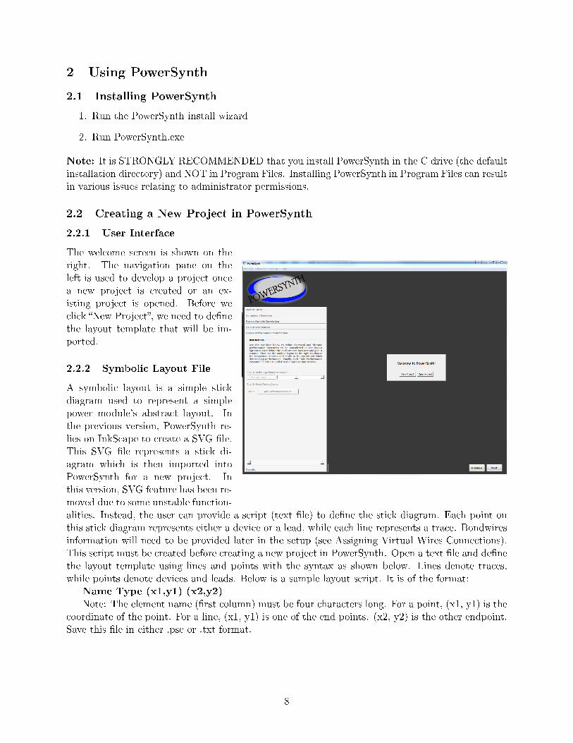
The welcome screen is shown on theright. The navigation pane on theleft is used to develop a project oncea new project is created or an ex-isting project is opened. Before weclick �New Project�, we need to de�nethe layout template that will be im-ported.
2.2.2 Symbolic Layout File
A symbolic layout is a simple stickdiagram used to represent a simplepower module's abstract layout. Inthe previous version, PowerSynth re-lies on InkScape to create a SVG �le.This SVG �le represents a stick di-agram which is then imported intoPowerSynth for a new project. Inthis version, SVG feature has been re-moved due to some unstable function-alities. Instead, the user can provide a script (text �le) to de�ne the stick diagram. Each point onthis stick diagram represents either a device or a lead, while each line represents a trace. Bondwiresinformation will need to be provided later in the setup (see Assigning Virtual Wires Connections).This script must be created before creating a new project in PowerSynth. Open a text �le and de�nethe layout template using lines and points with the syntax as shown below. Lines denote traces,while points denote devices and leads. Below is a sample layout script. It is of the format:
Name Type (x1,y1) (x2,y2)
Note: The element name (�rst column) must be four characters long. For a point, (x1, y1) is thecoordinate of the point. For a line, (x1, y1) is one of the end points. (x2, y2) is the other endpoint.Save this �le in either .psc or .txt format.
8
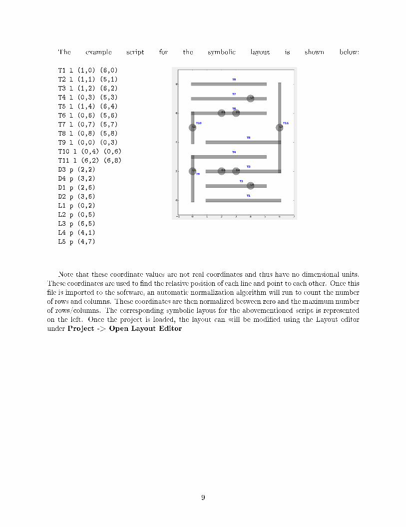
The example script for the symbolic layout is shown below:
T1 l (1,0) (6,0)
T2 l (1,1) (5,1)
T3 l (1,2) (6,2)
T4 l (0,3) (5,3)
T5 l (1,4) (6,4)
T6 l (0,6) (5,6)
T7 l (0,7) (5,7)
T8 l (0,8) (5,8)
T9 l (0,0) (0,3)
T10 l (0,4) (0,6)
T11 l (6,2) (6,8)
D3 p (2,2)
D4 p (3,2)
D1 p (2,6)
D2 p (3,6)
L1 p (0,2)
L2 p (0,5)
L3 p (6,5)
L4 p (4,1)
L5 p (4,7)
Note that these coordinate values are not real coordinates and thus have no dimensional units.These coordinates are used to �nd the relative position of each line and point to each other. Once this�le is imported to the software, an automatic normalization algorithm will run to count the numberof rows and columns. These coordinates are then normalized between zero and the maximum numberof rows/columns. The corresponding symbolic layout for the abovementioned script is representedon the left. Once the project is loaded, the layout can still be modi�ed using the Layout editorunder Project -> Open Layout Editor
9
2.2.3 Create a New Project
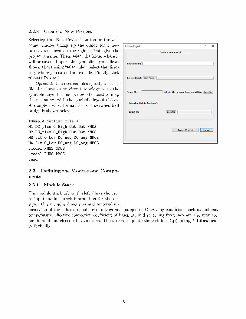
Selecting the �New Project� button on the wel-come window brings up the dialog for a newproject as shown on the right. First, give theproject a name. Then, select the folder where itwill be saved. Import the symbolic layout �le asshown above using �select �le�. Select the direc-tory where you saved the text �le. Finally, click�Create Project�.
Optional: The user can also specify a netlist�le that have same circuit topology with thesymbolic layout. This can be later used to mapthe net names with the symbolic layout object.A sample netlist format for a 4 switches halfbridge is shown below:
*Sample Netlist file:*
M1 DC_plus G_High Out Out NMOS
M2 DC_plus G_High Out Out NMOS
M3 Out G_Low DC_neg DC_neg NMOS
M4 Out G_Low DC_neg DC_neg NMOS
.model NMOS NMOS
.model PMOS PMOS
.end
2.3 De�ning the Module and Compo-nents
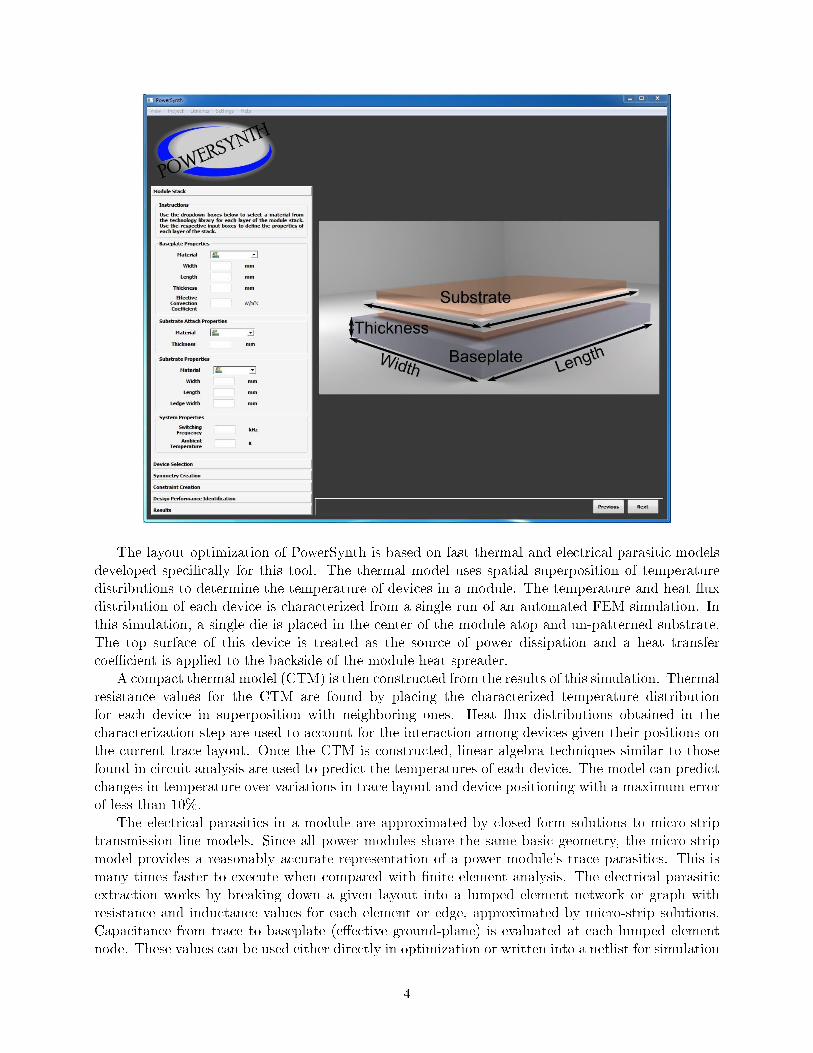
2.3.1 Module Stack
The module stack tab on the left allows the userto input module stack information for the de-sign. This includes dimension and material in-formation of the substrate, substrate attach and baseplate. Operating conditions such as ambienttemperature, e�ective convection coe�cient of baseplate and switching frequency are also requiredfor thermal and electrical evaluations. The user can update the tech �les (.p) using * Libraries-
>Tech lib.
10
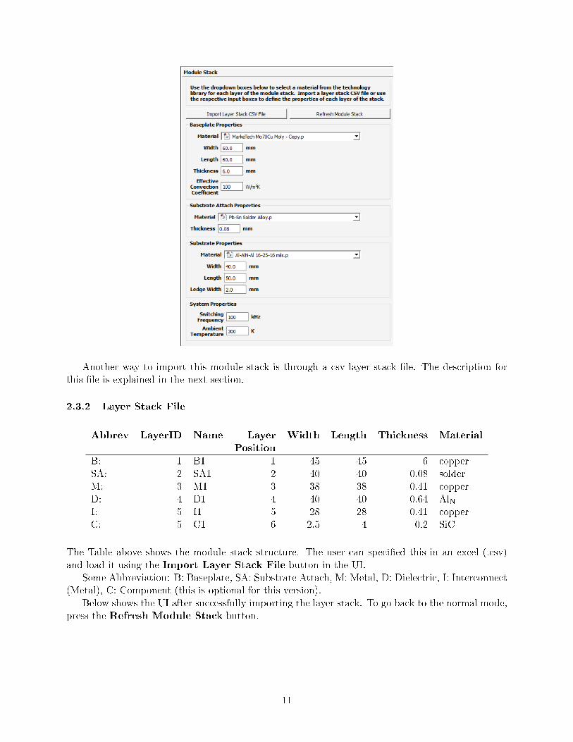
Another way to import this module stack is through a csv layer stack �le. The description forthis �le is explained in the next section.
2.3.2 Layer Stack File
Abbrev LayerID Name Layer Width Length Thickness Material
Position
B: 1 B1 1 45 45 6 copperSA: 2 SA1 2 40 40 0.08 solderM: 3 M1 3 38 38 0.41 copperD: 4 D1 4 40 40 0.64 AlNI: 5 I1 5 28 28 0.41 copperC: 5 C1 6 2.5 4 0.2 SiC
The Table above shows the module stack structure. The user can speci�ed this in an excel (.csv)and load it using the Import Layer Stack File button in the UI.
Some Abbreviation: B: Baseplate, SA: Substrate Attach, M: Metal, D: Dielectric, I: Interconnect(Metal), C: Component (this is optional for this version).
Below shows the UI after successfully importing the layer stack. To go back to the normal mode,press the Refresh Module Stack button.
11
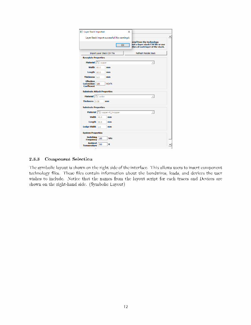
2.3.3 Component Selection
The symbolic layout is shown on the right side of the interface. This allows users to insert componenttechnology �les. These �les contain information about the bondwires, leads, and devices the userwishes to include. Notice that the names from the layout script for each traces and Devices areshown on the right-hand side. (Symbolic Layout)
12
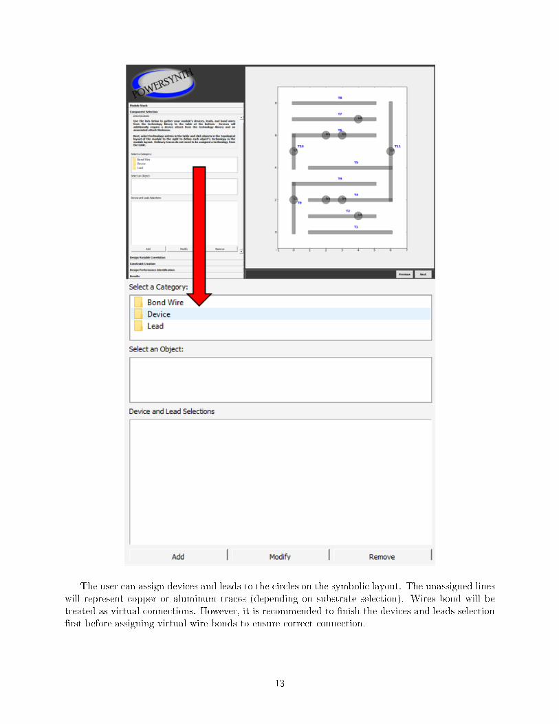
The user can assign devices and leads to the circles on the symbolic layout. The unassigned lineswill represent copper or aluminum traces (depending on substrate selection). Wires bond will betreated as virtual connections. However, it is recommended to �nish the devices and leads selection�rst before assigning virtual wire bonds to ensure correct connection.
13
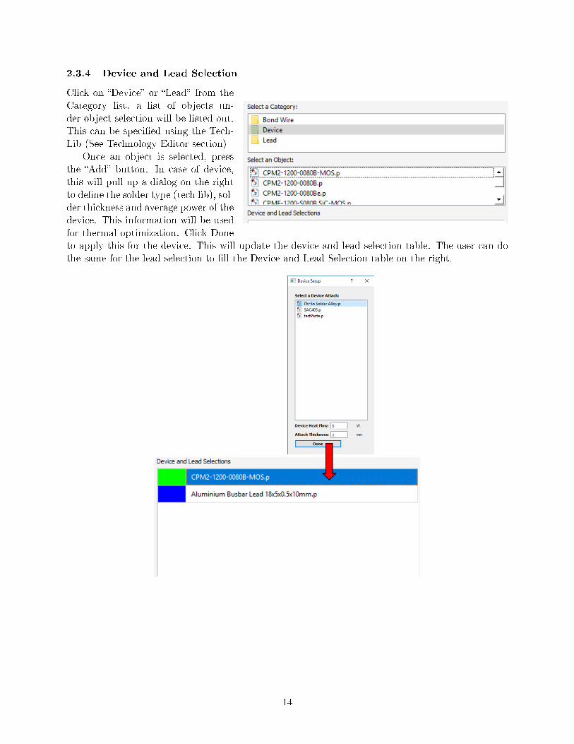
2.3.4 Device and Lead Selection
Click on �Device� or �Lead� from theCategory list, a list of objects un-der object selection will be listed out.This can be speci�ed using the Tech-Lib (See Technology Editor section)
Once an object is selected, pressthe �Add� button. In case of device,this will pull up a dialog on the rightto de�ne the solder type (tech lib), sol-der thickness and average power of thedevice. This information will be usedfor thermal optimization. Click Doneto apply this for the device. This will update the device and lead selection table. The user can dothe same for the lead selection to �ll the Device and Lead Selection table on the right.
14
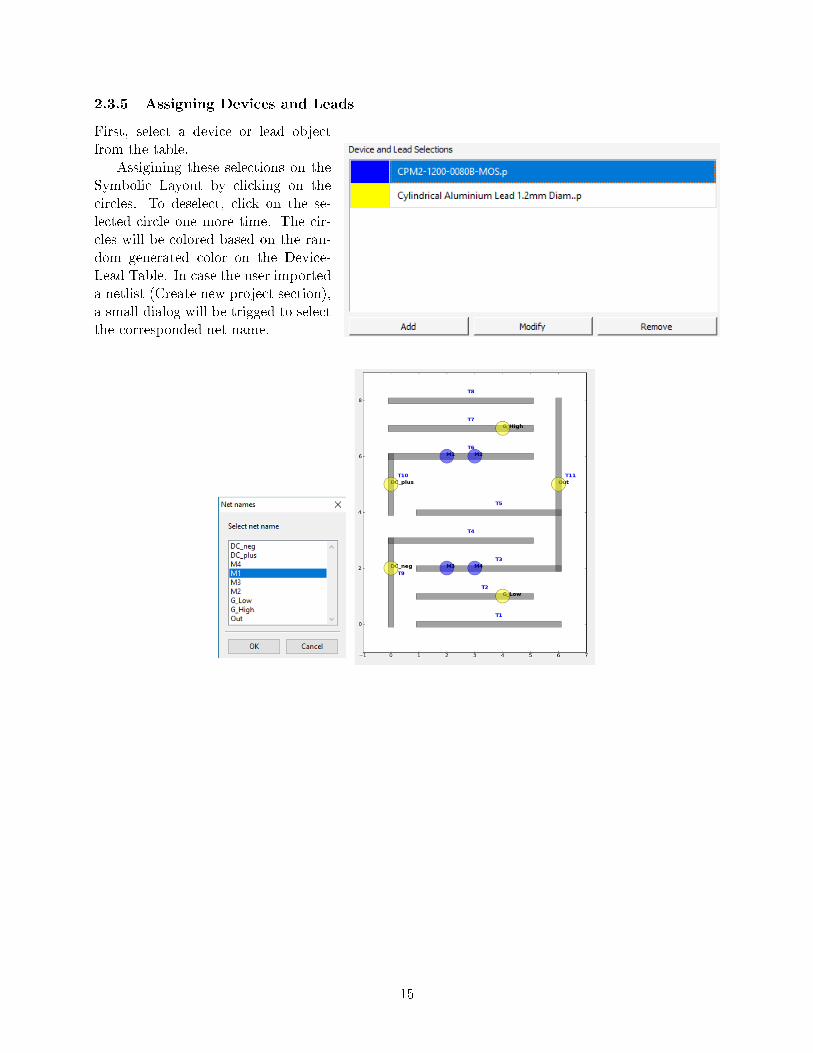
2.3.5 Assigning Devices and Leads
First, select a device or lead objectfrom the table.
Assigining these selections on theSymbolic Layout by clicking on thecircles. To deselect, click on the se-lected circle one more time. The cir-cles will be colored based on the ran-dom generated color on the Device-Lead Table. In case the user importeda netlist (Create new project section),a small dialog will be trigged to selectthe corresponded net name.
15
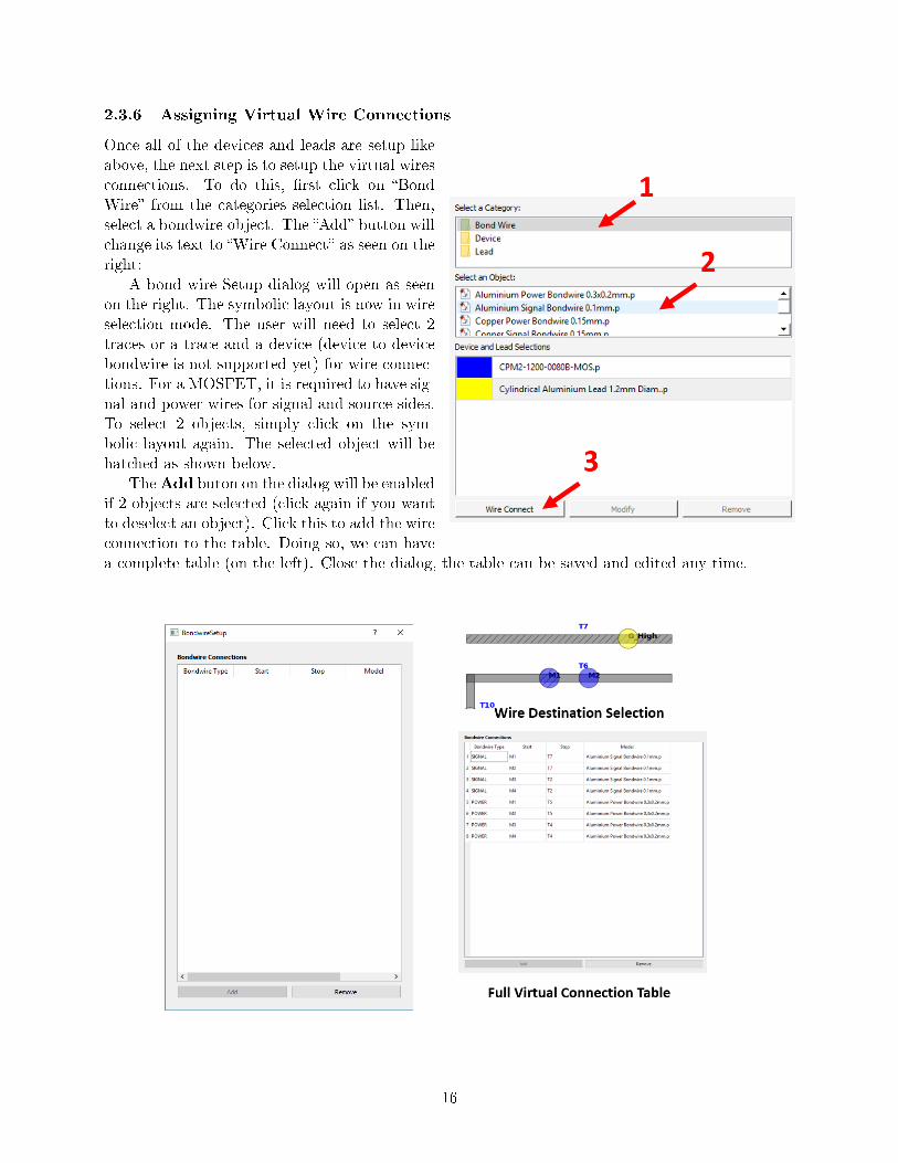
2.3.6 Assigning Virtual Wire Connections
Once all of the devices and leads are setup likeabove, the next step is to setup the virtual wiresconnections. To do this, �rst click on �BondWire� from the categories selection list. Then,select a bondwire object. The �Add� button willchange its text to �Wire Connect� as seen on theright:
A bond wire Setup dialog will open as seenon the right. The symbolic layout is now in wireselection mode. The user will need to select 2traces or a trace and a device (device to devicebondwire is not supported yet) for wire connec-tions. For a MOSFET, it is required to have sig-nal and power wires for signal and source sides.To select 2 objects, simply click on the sym-bolic layout again. The selected object will behatched as shown below.
TheAdd buton on the dialog will be enabledif 2 objects are selected (click again if you wantto deselect an object). Click this to add the wireconnection to the table. Doing so, we can havea complete table (on the left). Close the dialog, the table can be saved and edited any time.
16
2.4 De�ning Correlations and Constraints
2.4.1 Design Variable Correlation
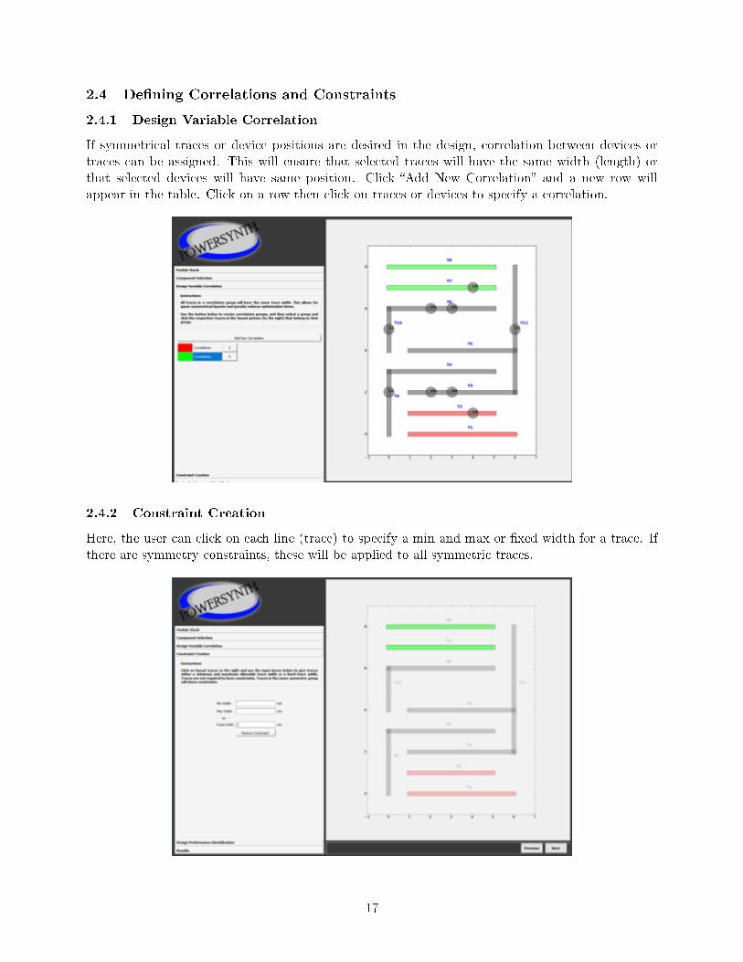
If symmetrical traces or device positions are desired in the design, correlation between devices ortraces can be assigned. This will ensure that selected traces will have the same width (length) orthat selected devices will have same position. Click �Add New Correlation� and a new row willappear in the table. Click on a row then click on traces or devices to specify a correlation.
2.4.2 Constraint Creation
Here, the user can click on each line (trace) to specify a min and max or �xed width for a trace. Ifthere are symmetry constraints, these will be applied to all symmetric traces.
17
2.5 Design Performance Identi�cation
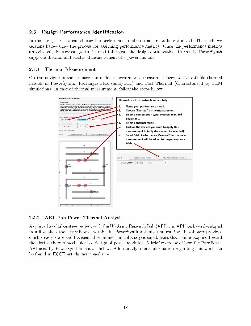
In this step, the user can choose the performance metrics that are to be optimized. The next twosections below show the process for assigning performance metrics. Once the performance metricsare selected, the user can go to the next tab to run the design optimization. Currently, PowerSynthsupports thermal and electrical measurement of a power module.
2.5.1 Thermal Measurement
On the navigation tool, a user can de�ne a performance measure. There are 2 available thermalmodels in PowerSynth: Rectangle Flux (analytical) and Fast Thermal (Characterized by FEMsimulation). In case of thermal measurement, follow the steps below:
2.5.2 ARL ParaPower Thermal Analysis
As part of a collaborative project with the US Army Research Lab (ARL), an API has been developedto utilize their tool, ParaPower, within the PowerSynth optimization routine. ParaPower providesquick steady-state and transient thermo-mechanical analysis capabilities that can be applied towardthe electro-thermo-mechanical co-design of power modules. A brief overview of how the ParaPowerAPI used by PowerSynth is shown below. Additionally, more information regarding this work canbe found in ECCE article mentioned in 4.
18
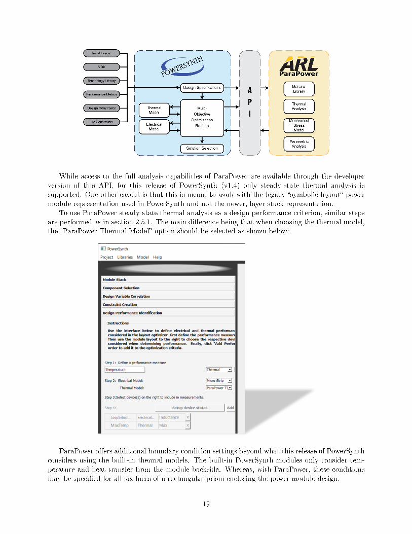
While access to the full analysis capabilities of ParaPower are available through the developerversion of this API, for this release of PowerSynth (v1.4) only steady-state thermal analysis issupported. One other caveat is that this is meant to work with the legacy �symbolic layout� powermodule representation used in PowerSynth and not the newer, layer-stack representation.
To use ParaPower steady-state thermal analysis as a design performance criterion, similar stepsare performed as in section 2.5.1. The main di�erence being that when choosing the thermal model,the �ParaPower Thermal Model� option should be selected as shown below:
ParaPower o�ers additional boundary condition settings beyond what this release of PowerSynthconsiders using the built-in thermal models. The built-in PowerSynth modules only consider tem-perature and heat transfer from the module backside. Whereas, with ParaPower, these conditionsmay be speci�ed for all six faces of a rectangular prism enclosing the power module design.
19
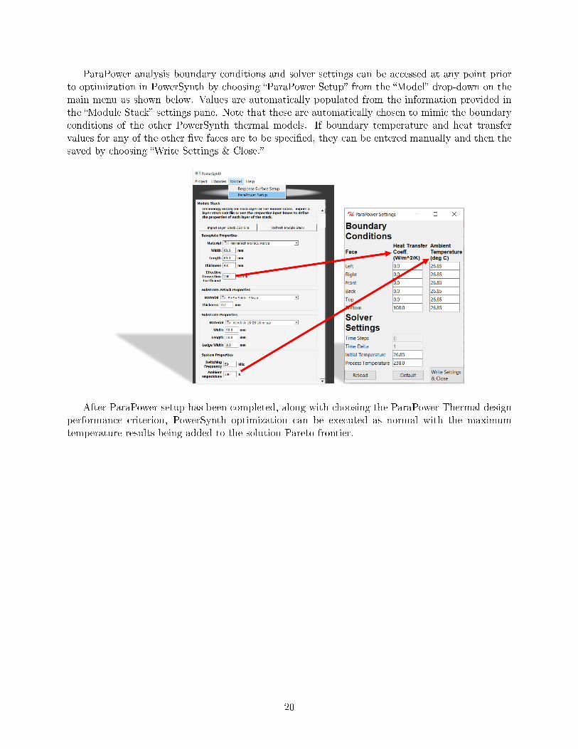
ParaPower analysis boundary conditions and solver settings can be accessed at any point priorto optimization in PowerSynth by choosing �ParaPower Setup� from the �Model� drop-down on themain menu as shown below. Values are automatically populated from the information provided inthe �Module Stack� settings pane. Note that these are automatically chosen to mimic the boundaryconditions of the other PowerSynth thermal models. If boundary temperature and heat transfervalues for any of the other �ve faces are to be speci�ed, they can be entered manually and then thesaved by choosing �Write Settings & Close.�
After ParaPower setup has been completed, along with choosing the ParaPower Thermal designperformance criterion, PowerSynth optimization can be executed as normal with the maximumtemperature results being added to the solution Pareto frontier.
20
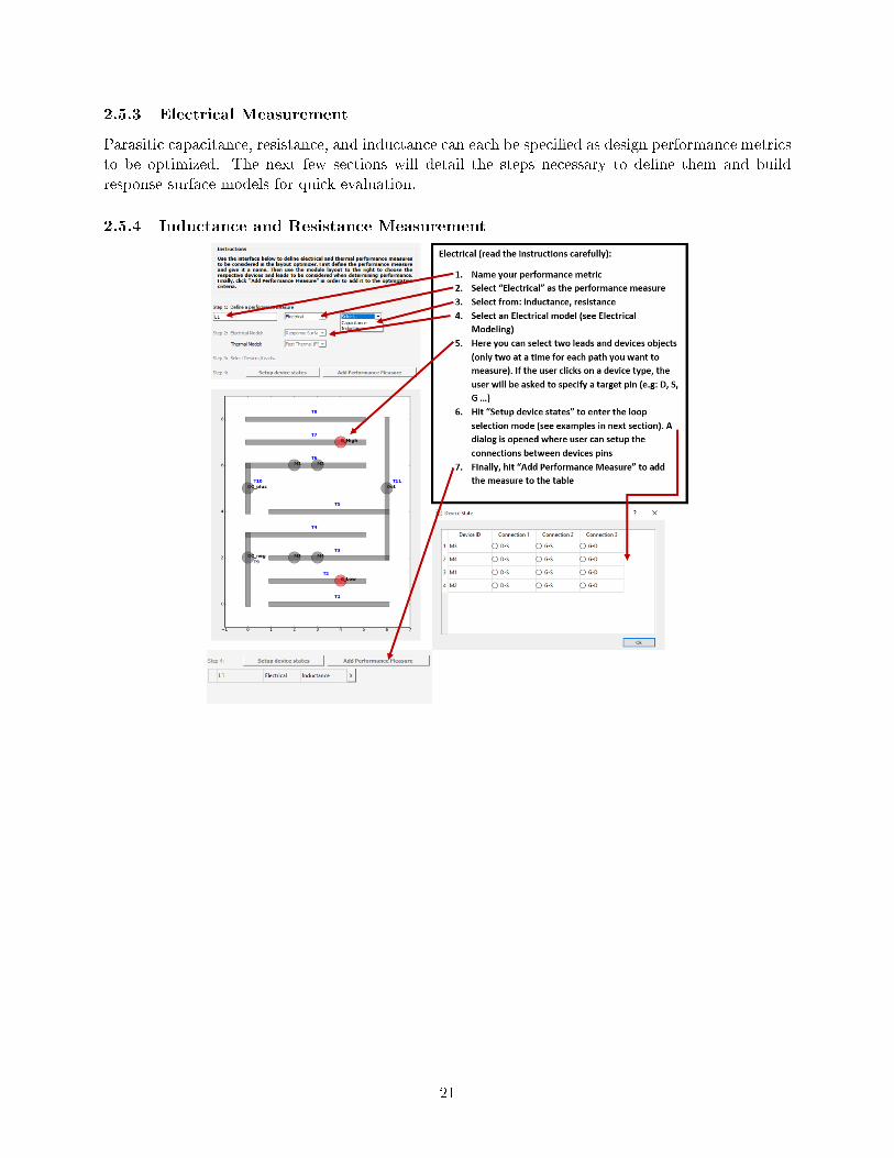
2.5.3 Electrical Measurement
Parasitic capacitance, resistance, and inductance can each be speci�ed as design performance metricsto be optimized. The next few sections will detail the steps necessary to de�ne them and buildresponse surface models for quick evaluation.
2.5.4 Inductance and Resistance Measurement
21
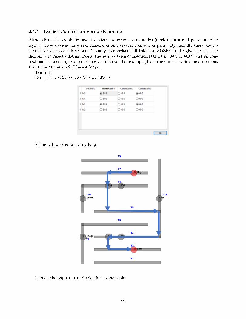
2.5.5 Device Connection Setup (Example)
Although on the symbolic layout devices are represent as nodes (circles), in a real power modulelayout, these devices have real dimension and several connection pads. By default, there are noconnections between these pads (usually a capacitance if this is a MOSFET). To give the user the�exibility to select di�erent loops, the setup device connection feature is used to select virtual con-nections between any two pins of a given devices. For example, from the same electrical measurementabove, we can setup 2 di�erent loops.
Loop 1:
Setup the device connections as follows:
We now have the following loop:
Name this loop as L1 and add this to the table.
22
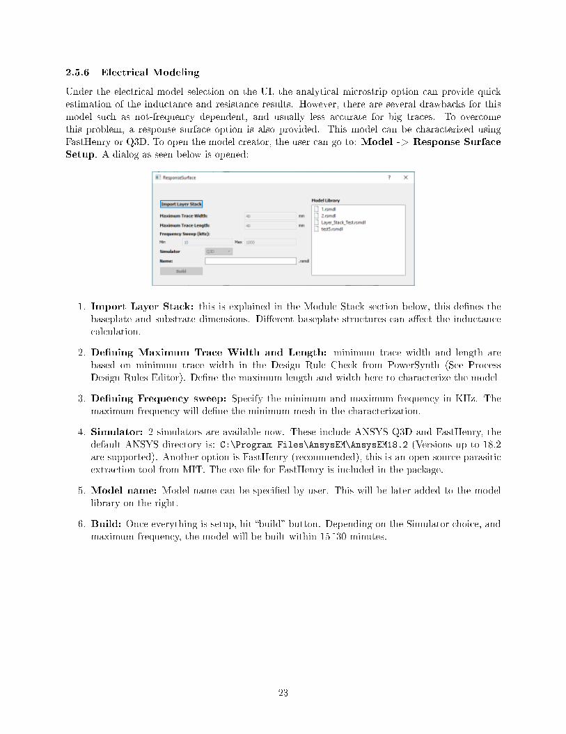
2.5.6 Electrical Modeling
Under the electrical model selection on the UI, the analytical microstrip option can provide quickestimation of the inductance and resistance results. However, there are several drawbacks for thismodel such as not-frequency dependent, and usually less accurate for big traces. To overcomethis problem, a response surface option is also provided. This model can be characterized usingFastHenry or Q3D. To open the model creator, the user can go to: Model -> Response Surface
Setup. A dialog as seen below is opened:
1. Import Layer Stack: this is explained in the Module Stack section below, this de�nes thebaseplate and substrate dimensions. Di�erent baseplate structures can a�ect the inductancecalculation.
2. De�ning Maximum Trace Width and Length: minimum trace width and length arebased on minimum trace width in the Design Rule Check from PowerSynth (See ProcessDesign Rules Editor). De�ne the maximum length and width here to characterize the model
3. De�ning Frequency sweep: Specify the minimum and maximum frequency in KHz. Themaximum frequency will de�ne the minimum mesh in the characterization.
4. Simulator: 2 simulators are available now. These include ANSYS Q3D and FastHenry, thedefault ANSYS directory is: C:\Program Files\AnsysEM\AnsysEM18.2 (Versions up to 18.2are supported). Another option is FastHenry (recommended), this is an open source parasiticextraction tool from MIT. The exe �le for FastHenry is included in the package.
5. Model name: Model name can be speci�ed by user. This will be later added to the modellibrary on the right.
6. Build: Once everything is setup, hit �build� button. Depending on the Simulator choice, andmaximum frequency, the model will be built within 15~30 minutes.
23
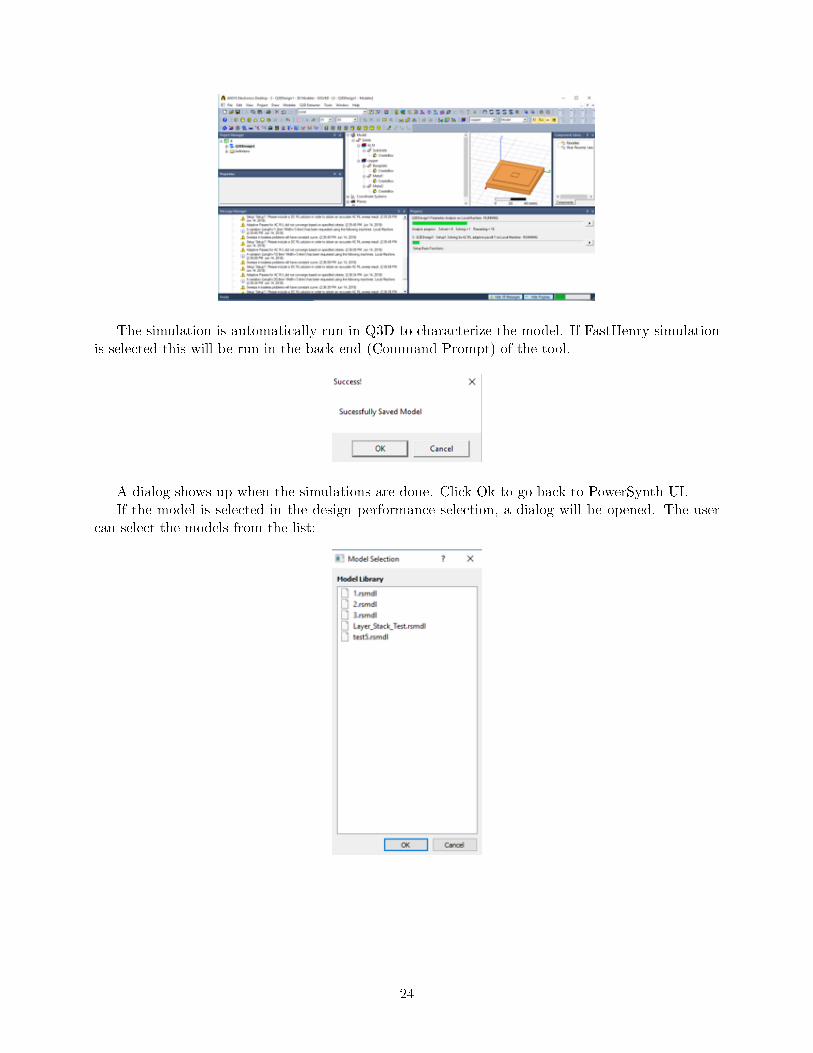
The simulation is automatically run in Q3D to characterize the model. If FastHenry simulationis selected this will be run in the back-end (Command Prompt) of the tool.
A dialog shows up when the simulations are done. Click Ok to go back to PowerSynth UI.If the model is selected in the design performance selection, a dialog will be opened. The user
can select the models from the list:
24
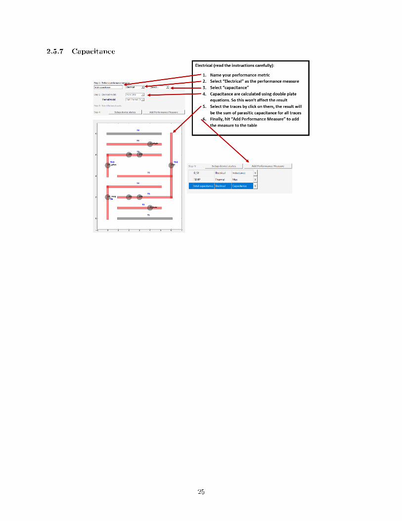
2.5.7 Capacitance
25
2.6 Constraint-Aware Layout Engine (Beta-Version)
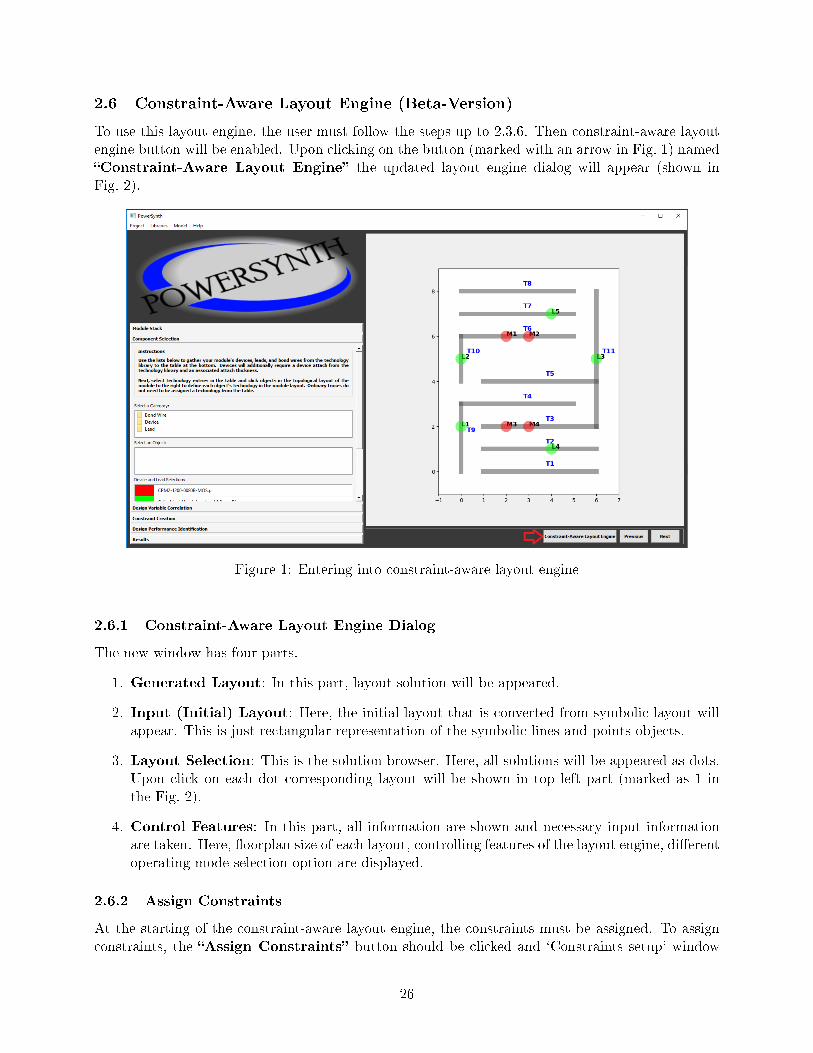
To use this layout engine, the user must follow the steps up to 2.3.6. Then constraint-aware layoutengine button will be enabled. Upon clicking on the button (marked with an arrow in Fig. 1) named�Constraint-Aware Layout Engine� the updated layout engine dialog will appear (shown inFig. 2).
Figure 1: Entering into constraint-aware layout engine
2.6.1 Constraint-Aware Layout Engine Dialog
The new window has four parts.
1. Generated Layout: In this part, layout solution will be appeared.
2. Input (Initial) Layout: Here, the initial layout that is converted from symbolic layout willappear. This is just rectangular representation of the symbolic lines and points objects.
3. Layout Selection: This is the solution browser. Here, all solutions will be appeared as dots.Upon click on each dot corresponding layout will be shown in top left part (marked as 1 inthe Fig. 2).
4. Control Features: In this part, all information are shown and necessary input informationare taken. Here, �oorplan size of each layout, controlling features of the layout engine, di�erentoperating mode selection option are displayed.
2.6.2 Assign Constraints
At the starting of the constraint-aware layout engine, the constraints must be assigned. To assignconstraints, the �Assign Constraints� button should be clicked and `Constraints setup' window
26
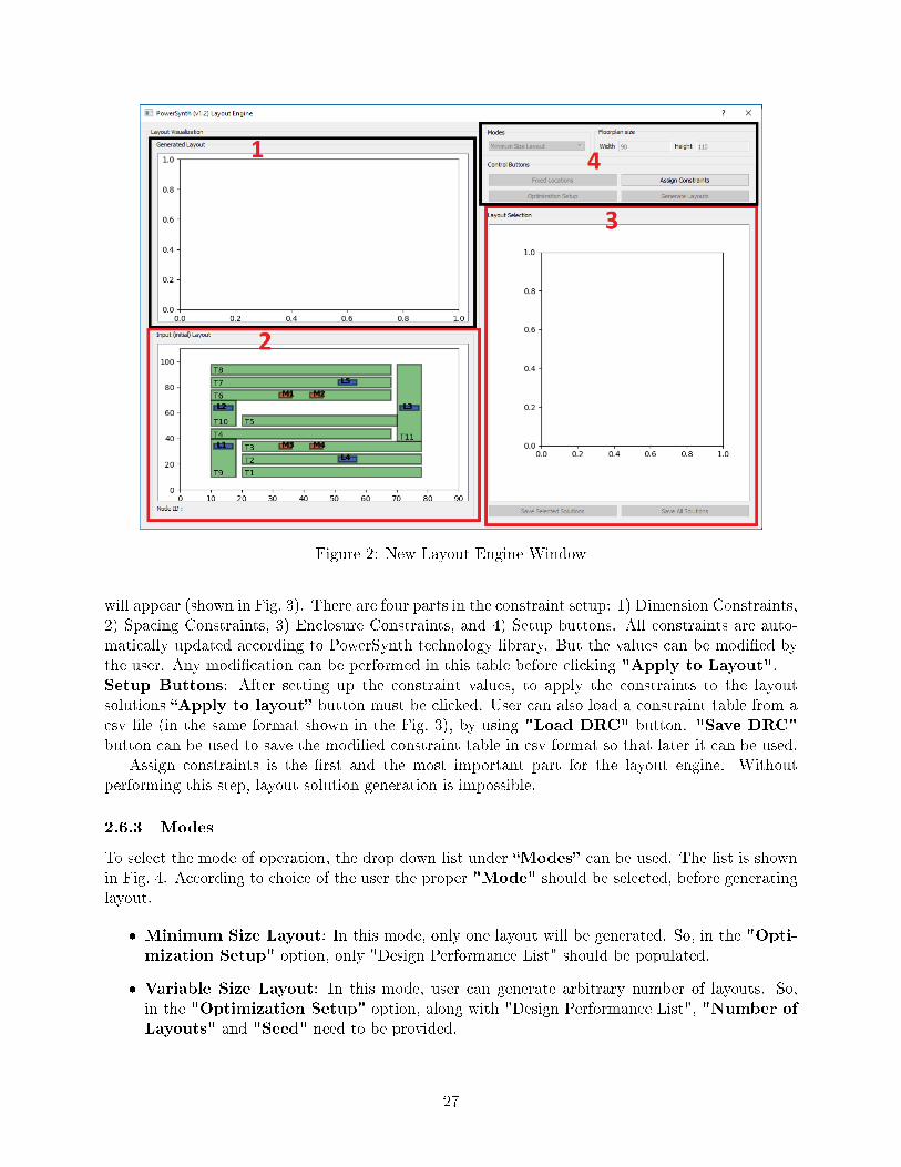
Figure 2: New Layout Engine Window
will appear (shown in Fig. 3). There are four parts in the constraint setup: 1) Dimension Constraints,2) Spacing Constraints, 3) Enclosure Constraints, and 4) Setup buttons. All constraints are auto-matically updated according to PowerSynth technology library. But the values can be modi�ed bythe user. Any modi�cation can be performed in this table before clicking "Apply to Layout".Setup Buttons: After setting up the constraint values, to apply the constraints to the layoutsolutions �Apply to layout� button must be clicked. User can also load a constraint table from acsv �le (in the same format shown in the Fig. 3), by using "Load DRC" button. "Save DRC"button can be used to save the modi�ed constraint table in csv format so that later it can be used.
Assign constraints is the �rst and the most important part for the layout engine. Withoutperforming this step, layout solution generation is impossible.
2.6.3 Modes
To select the mode of operation, the drop down list under �Modes� can be used. The list is shownin Fig. 4. According to choice of the user the proper "Mode" should be selected, before generatinglayout.
� Minimum Size Layout: In this mode, only one layout will be generated. So, in the "Opti-mization Setup" option, only "Design Performance List" should be populated.
� Variable Size Layout: In this mode, user can generate arbitrary number of layouts. So,in the "Optimization Setup" option, along with "Design Performance List", "Number ofLayouts" and "Seed" need to be provided.
27
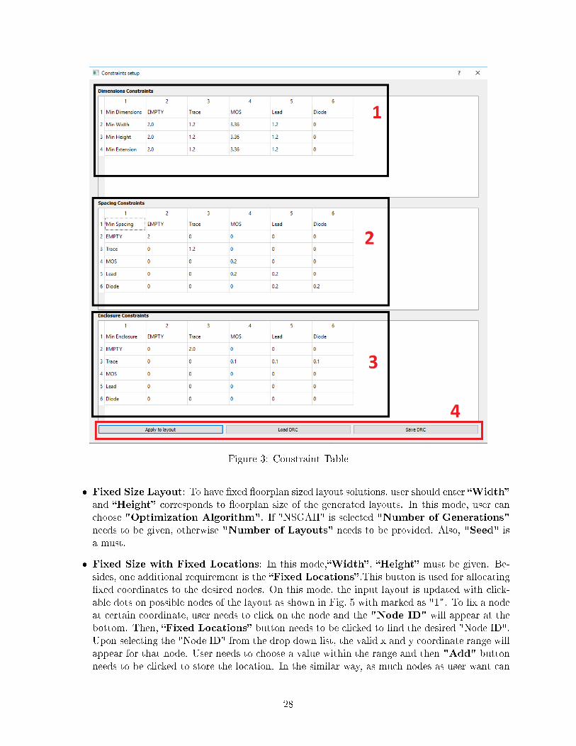
Figure 3: Constraint Table
� Fixed Size Layout: To have �xed �oorplan sized layout solutions, user should enter �Width�
and �Height� corresponds to �oorplan size of the generated layouts. In this mode, user canchoose "Optimization Algorithm". If "NSGAII" is selected "Number of Generations"needs to be given, otherwise "Number of Layouts" needs to be provided. Also, "Seed" isa must.
� Fixed Size with Fixed Locations: In this mode,�Width� , �Height� must be given. Be-sides, one additional requirement is the �Fixed Locations� .This button is used for allocating�xed coordinates to the desired nodes. On this mode, the input layout is updated with click-able dots on possible nodes of the layout as shown in Fig. 5 with marked as "1". To �x a nodeat certain coordinate, user needs to click on the node and the "Node ID" will appear at thebottom. Then, �Fixed Locations� button needs to be clicked to �nd the desired "Node ID".Upon selecting the "Node ID" from the drop down list, the valid x and y coordinate range willappear for that node. User needs to choose a value within the range and then "Add" buttonneeds to be clicked to store the location. In the similar way, as much nodes as user want can
28
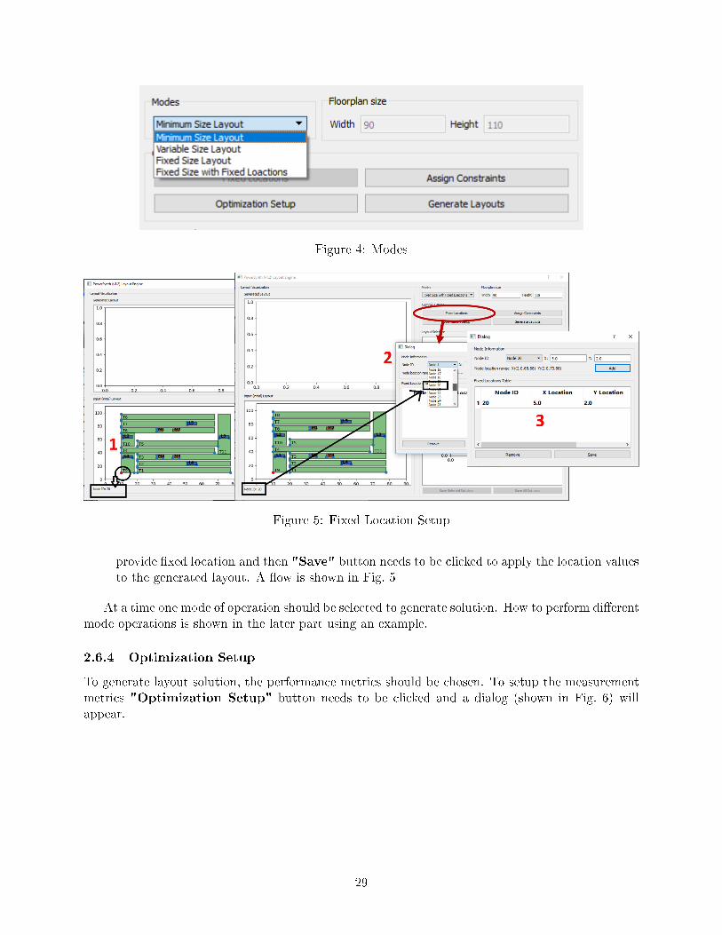
Figure 4: Modes
Figure 5: Fixed Location Setup
provide �xed location and then "Save" button needs to be clicked to apply the location valuesto the generated layout. A �ow is shown in Fig. 5
At a time one mode of operation should be selected to generate solution. How to perform di�erentmode operations is shown in the later part using an example.
2.6.4 Optimization Setup
To generate layout solution, the performance metrics should be chosen. To setup the measurementmetrics "Optimization Setup" button needs to be clicked and a dialog (shown in Fig. 6) willappear.
29
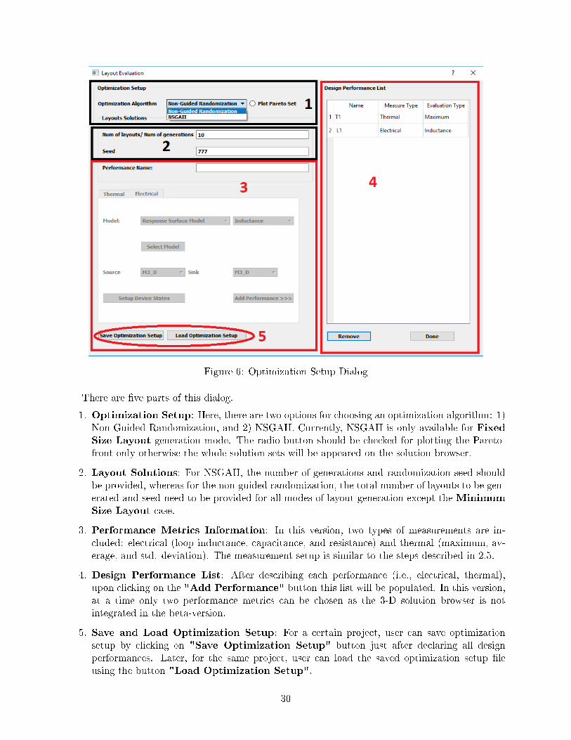
Figure 6: Optimization Setup Dialog
There are �ve parts of this dialog.
1. Optimization Setup: Here, there are two options for choosing an optimization algorithm: 1)Non-Guided Randomization, and 2) NSGAII. Currently, NSGAII is only available for FixedSize Layout generation mode. The radio button should be checked for plotting the Pareto-front only otherwise the whole solution sets will be appeared on the solution browser.
2. Layout Solutions: For NSGAII, the number of generations and randomization seed shouldbe provided, whereas for the non-guided randomization, the total number of layouts to be gen-erated and seed need to be provided for all modes of layout generation except the Minimum
Size Layout case.
3. Performance Metrics Information: In this version, two types of measurements are in-cluded: electrical (loop inductance, capacitance, and resistance) and thermal (maximum, av-erage, and std. deviation). The measurement setup is similar to the steps described in 2.5.
4. Design Performance List: After describing each performance (i.e., electrical, thermal),upon clicking on the "Add Performance" button this list will be populated. In this version,at a time only two performance metrics can be chosen as the 3-D solution browser is notintegrated in the beta-version.
5. Save and Load Optimization Setup: For a certain project, user can save optimizationsetup by clicking on "Save Optimization Setup" button just after declaring all designperformances. Later, for the same project, user can load the saved optimization setup �leusing the button "Load Optimization Setup".
30
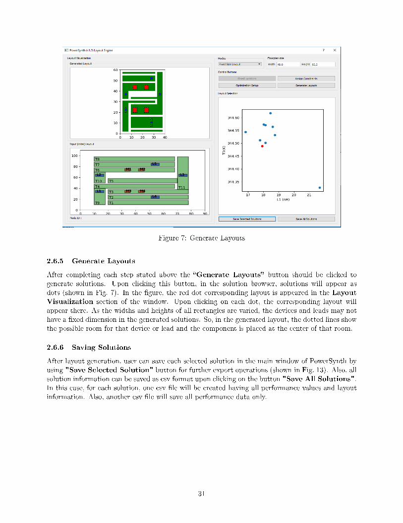
Figure 7: Generate Layouts
2.6.5 Generate Layouts
After completing each step stated above the �Generate Layouts� button should be clicked togenerate solutions. Upon clicking this button, in the solution browser, solutions will appear asdots (shown in Fig. 7). In the �gure, the red dot corresponding layout is appeared in the LayoutVisualization section of the window. Upon clicking on each dot, the corresponding layout willappear there. As the widths and heights of all rectangles are varied, the devices and leads may nothave a �xed dimension in the generated solutions. So, in the generated layout, the dotted lines showthe possible room for that device or lead and the component is placed at the center of that room.
2.6.6 Saving Solutions
After layout generation, user can save each selected solution in the main window of PowerSynth byusing "Save Selected Solution" button for further export operations (shown in Fig. 13). Also, allsolution information can be saved as csv format upon clicking on the button "Save All Solutions".In this case, for each solution, one csv �le will be created having all performance values and layoutinformation. Also, another csv �le will save all performance data only.
31
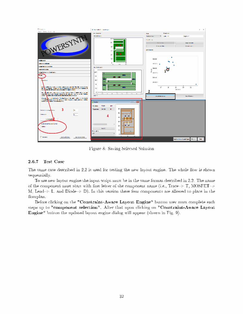
Figure 8: Saving Selected Solution
2.6.7 Test Case
The same case described in 2.2 is used for testing the new layout engine. The whole �ow is shownsequentially.
To use new layout engine the input script must be in the same format described in 2.2. The nameof the component must start with �rst letter of the component name (i.e., Trace�> T, MOSFET�>M, Lead�> L, and Diode�> D). In this version these four components are allowed to place in the�oorplan.
Before clicking on the "Constraint-Aware Layout Engine" button user must complete eachsteps up to "component selection". After that upon clicking on "Constraint-Aware LayoutEngine" button the updated layout engine dialog will appear (shown in Fig. 9).
32
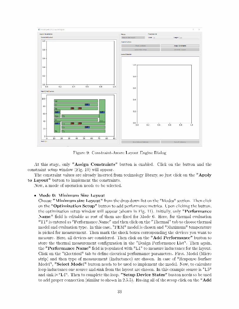
Figure 9: Constraint-Aware Layout Engine Dialog
At this stage, only "Assign Constraints" button is enabled. Click on the button and theconstraint setup window (Fig. 10) will appear.
The constraint values are already inserted from technology library, so just click on the "Applyto Layout" button to implement the constraints.
Now, a mode of operation needs to be selected.
� Mode 0: Minimum Size Layout
Choose "Minimum size Layout" from the drop down list on the "Modes" section. Then clickon the "Optimization Setup" button to add performance metrics. Upon clicking the button,the optimization setup window will appear (shown in Fig. 11). Initially, only "Performance
Name" �eld is editable as rest of them are �xed for Mode 0. Here, for thermal evaluation"T1" is entered as "Performance Name" and then click on the "Thermal" tab to choose thermalmodel and evaluation type. In this case, "FEM" model is chosen and "Maximum" temperatureis picked for measurement. Then mark the check boxes corresponding the devices you want tomeasure. Here, all devices are considered. Then click on the "Add Performance" button tostore the thermal measurement con�guration in the "Design Performance List". Then again,the "Performance Name" �eld is populated with "L1" to measure inductance for the layout.Click on the "Electrical" tab to de�ne electrical performance parameters. First, Model (Microstrip) and then type of measurement (Inductance) are chosen. In case of "Response SurfaceModel", "Select Model" button needs to be used to implement the model. Now, to calculateloop inductance one source and sink from the layout are chosen. In this example source is "L5"and sink is "L4". Then to complete the loop, "Setup Device States" button needs to be usedto add proper connection (similar to shown in 2.5.5). Having all of the setup click on the "Add
33
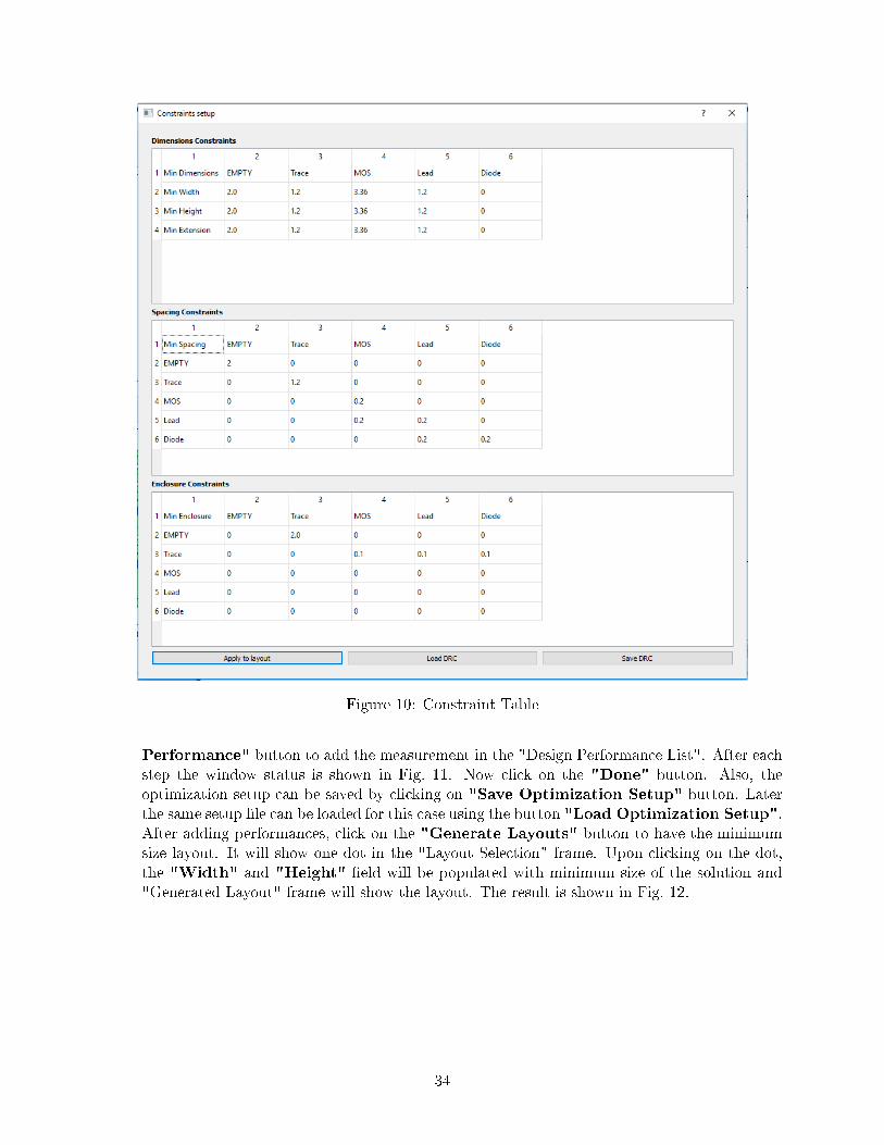
Figure 10: Constraint Table
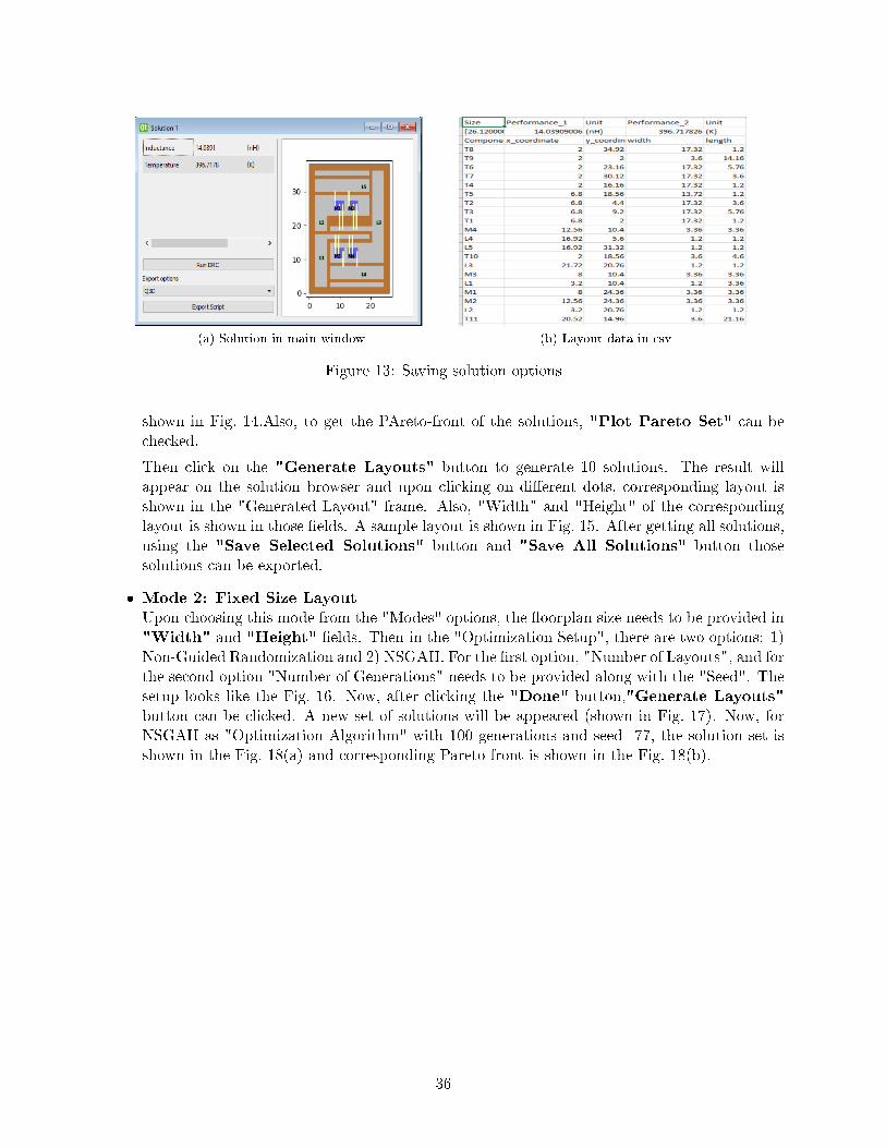
Performance" button to add the measurement in the "Design Performance List". After eachstep the window status is shown in Fig. 11. Now click on the "Done" button. Also, theoptimization setup can be saved by clicking on "Save Optimization Setup" button. Laterthe same setup �le can be loaded for this case using the button "Load Optimization Setup".After adding performances, click on the "Generate Layouts" button to have the minimumsize layout. It will show one dot in the "Layout Selection" frame. Upon clicking on the dot,the "Width" and "Height" �eld will be populated with minimum size of the solution and"Generated Layout" frame will show the layout. The result is shown in Fig. 12.
34
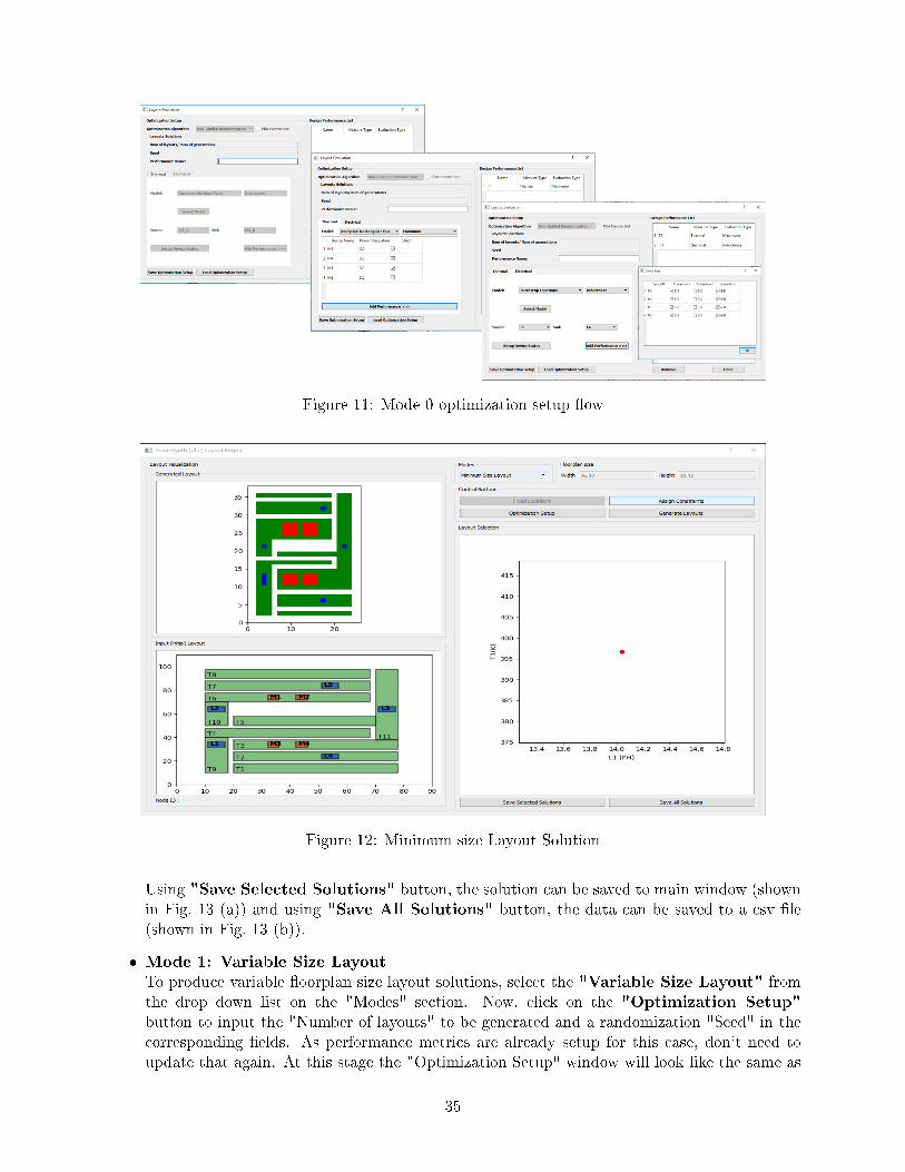
Figure 11: Mode 0 optimization setup �ow
Figure 12: Minimum size Layout Solution
Using "Save Selected Solutions" button, the solution can be saved to main window (shownin Fig. 13 (a)) and using "Save All Solutions" button, the data can be saved to a csv �le(shown in Fig. 13 (b)).
� Mode 1: Variable Size Layout
To produce variable �oorplan size layout solutions, select the "Variable Size Layout" fromthe drop down list on the "Modes" section. Now, click on the "Optimization Setup"
button to input the "Number of layouts" to be generated and a randomization "Seed" in thecorresponding �elds. As performance metrics are already setup for this case, don't need toupdate that again. At this stage the "Optimization Setup" window will look like the same as
35
(a) Solution in main window (b) Layout data in csv
Figure 13: Saving solution options
shown in Fig. 14.Also, to get the PAreto-front of the solutions, "Plot Pareto Set" can bechecked.
Then click on the "Generate Layouts" button to generate 10 solutions. The result willappear on the solution browser and upon clicking on di�erent dots, corresponding layout isshown in the "Generated Layout" frame. Also, "Width" and "Height" of the correspondinglayout is shown in those �elds. A sample layout is shown in Fig. 15. After getting all solutions,using the "Save Selected Solutions" button and "Save All Solutions" button thosesolutions can be exported.
� Mode 2: Fixed Size Layout
Upon choosing this mode from the "Modes" options, the �oorplan size needs to be provided in"Width" and "Height" �elds. Then in the "Optimization Setup", there are two options: 1)Non-Guided Randomization and 2) NSGAII. For the �rst option, "Number of Layouts", and forthe second option "Number of Generations" needs to be provided along with the "Seed". Thesetup looks like the Fig. 16. Now, after clicking the "Done" button,"Generate Layouts"
button can be clicked. A new set of solutions will be appeared (shown in Fig. 17). Now, forNSGAII as "Optimization Algorithm" with 100 generations and seed=77, the solution set isshown in the Fig. 18(a) and corresponding Pareto-front is shown in the Fig. 18(b).
36
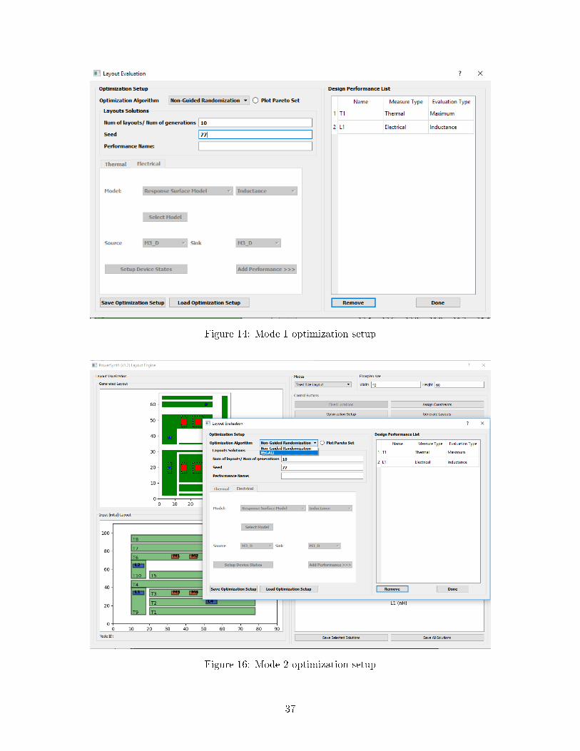
Figure 14: Mode 1 optimization setup
Figure 16: Mode 2 optimization setup
37
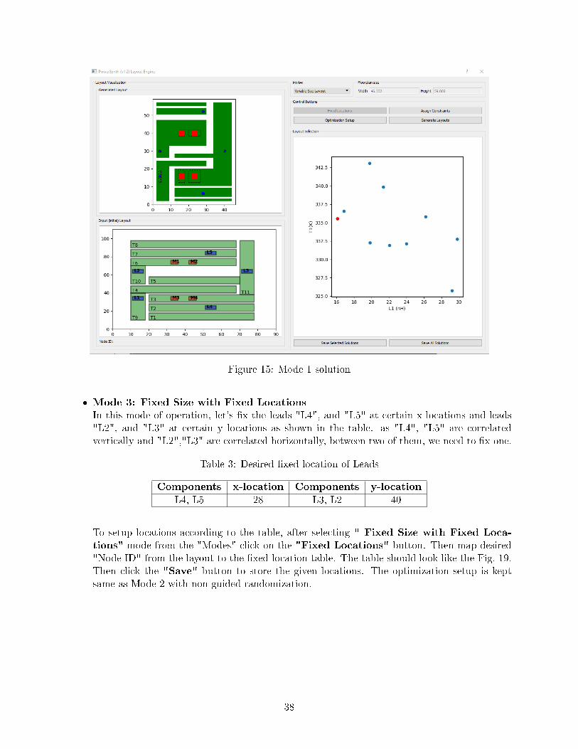
Figure 15: Mode 1 solution
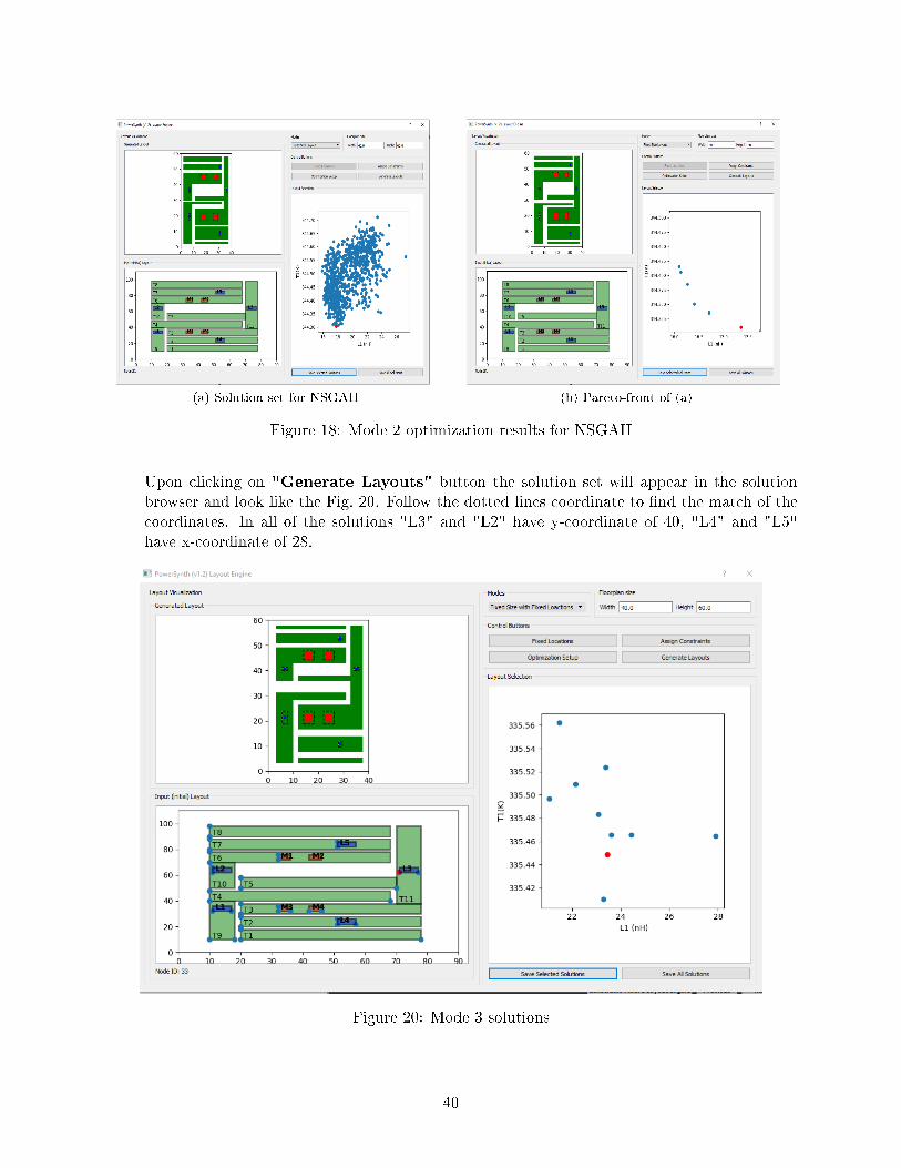
� Mode 3: Fixed Size with Fixed Locations
In this mode of operation, let's �x the leads "L4", and "L5" at certain x locations and leads"L2", and "L3" at certain y locations as shown in the table. as "L4", "L5" are correlatedvertically and "L2","L3" are correlated horizontally, between two of them, we need to �x one.
Table 3: Desired �xed location of Leads
Components x-location Components y-location
L4, L5 28 L3, L2 40
To setup locations according to the table, after selecting " Fixed Size with Fixed Loca-
tions" mode from the "Modes" click on the "Fixed Locations" button. Then map desired"Node ID" from the layout to the �xed location table. The table should look like the Fig. 19.Then click the "Save" button to store the given locations. The optimization setup is keptsame as Mode 2 with non-guided randomization.
38
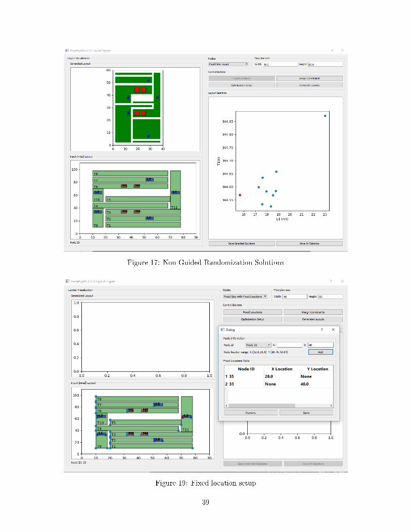
Figure 17: Non-Guided Randomization Solutions
Figure 19: Fixed location setup
39
(a) Solution set for NSGAII (b) Pareto-front of (a)
Figure 18: Mode 2 optimization results for NSGAII
Upon clicking on "Generate Layouts" button the solution set will appear in the solutionbrowser and look like the Fig. 20. Follow the dotted lines coordinate to �nd the match of thecoordinates. In all of the solutions "L3" and "L2" have y-coordinate of 40, "L4" and "L5"have x-coordinate of 28.
Figure 20: Mode 3 solutions
40
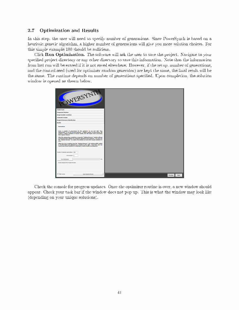
2.7 Optimization and Results
In this step, the user will need to specify number of generations. Since PowerSynth is based on aheuristic genetic algorithm, a higher number of generations will give you more solution choices. Forthis simple example 100 should be su�cient.
Click Run Optimization. The software will ask the user to save the project. Navigate to yourspeci�ed project directory or any other directory to save this information. Note that the informationfrom last run will be erased if it is not saved elsewhere. However, if the setup, number of generations,and the control seed (used for optimizer random generator) are kept the same, the �nal result will bethe same. The runtime depends on number of generations speci�ed. Upon completion, the solutionwindow is opened as shown below.
Check the console for progress updates. Once the optimizer routine is over, a new window shouldappear. Check your task bar if the window does not pop up. This is what the window may look like(depending on your unique solutions).
41
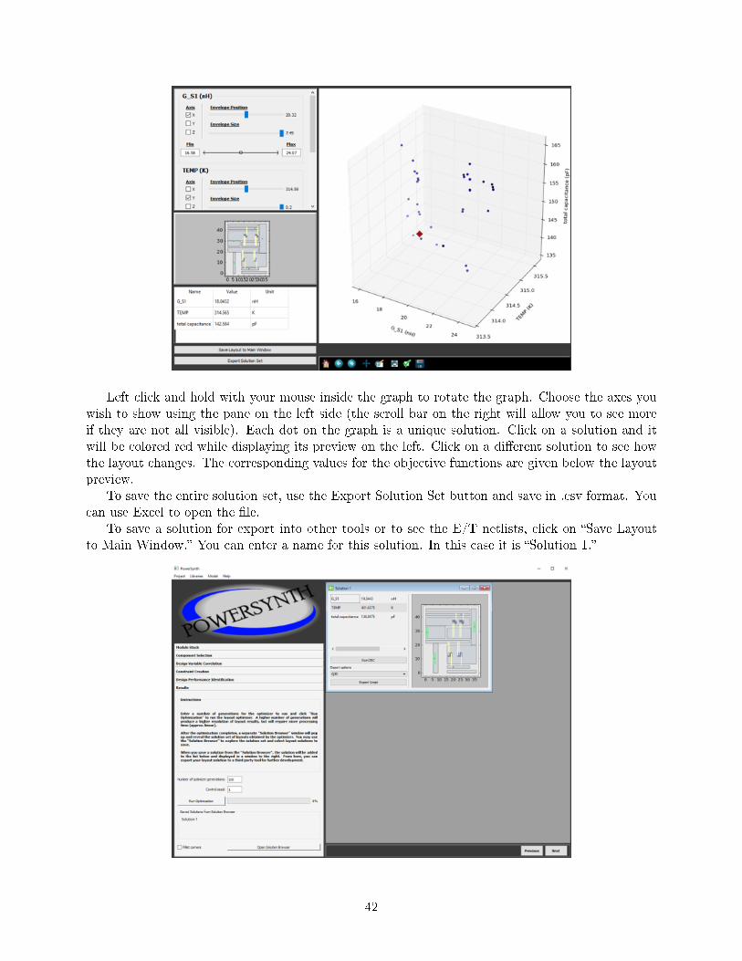
Left click and hold with your mouse inside the graph to rotate the graph. Choose the axes youwish to show using the pane on the left side (the scroll bar on the right will allow you to see moreif they are not all visible). Each dot on the graph is a unique solution. Click on a solution and itwill be colored red while displaying its preview on the left. Click on a di�erent solution to see howthe layout changes. The corresponding values for the objective functions are given below the layoutpreview.
To save the entire solution set, use the Export Solution Set button and save in .csv format. Youcan use Excel to open the �le.
To save a solution for export into other tools or to see the E/T netlists, click on �Save Layoutto Main Window.� You can enter a name for this solution. In this case it is �Solution 1.�
42
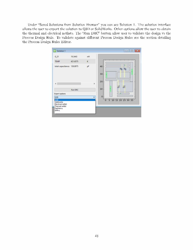
Under �Saved Solutions from Solution Browser� you can see Solution 1. The solution interfaceallows the user to export the solution to Q3D or SolidWorks. Other options allow the user to obtainthe thermal and electrical netlists. The �Run DRC� button allow user to validate the design vs theProcess Design Rule. To validate against di�erent Process Design Rules see the section detailingthe Process Design Rules Editor.
43
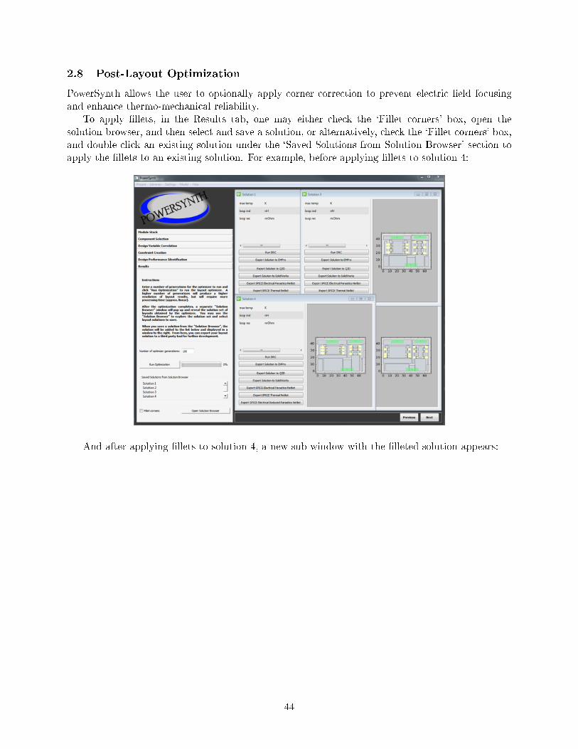
2.8 Post-Layout Optimization
PowerSynth allows the user to optionally apply corner correction to prevent electric �eld focusingand enhance thermo-mechanical reliability.
To apply �llets, in the Results tab, one may either check the `Fillet corners' box, open thesolution browser, and then select and save a solution, or alternatively, check the `Fillet corners' box,and double click an existing solution under the `Saved Solutions from Solution Browser' section toapply the �llets to an existing solution. For example, before applying �llets to solution 4:
And after applying �llets to solution 4, a new sub-window with the �lleted solution appears:
44
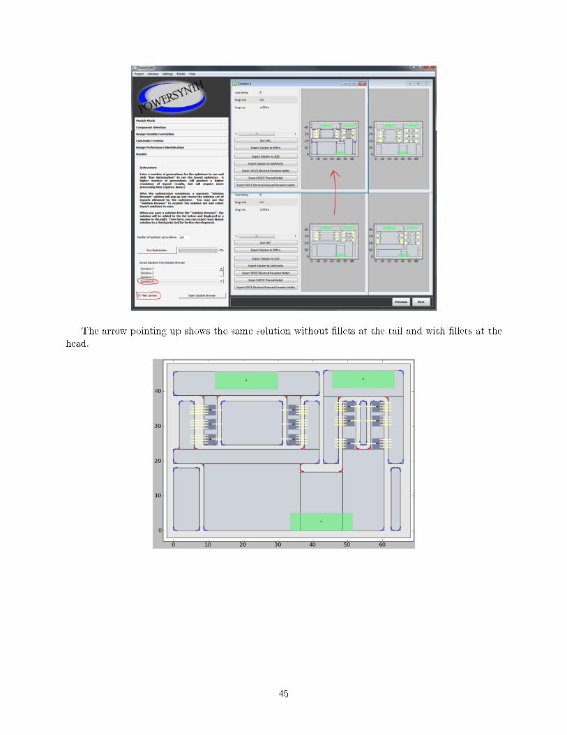
The arrow pointing up shows the same solution without �llets at the tail and with �llets at thehead.
45
2.9 Exporting Saved Solutions
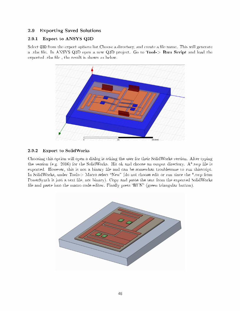
2.9.1 Export to ANSYS Q3D
Select Q3D from the export options list.Choose a directory, and create a �le name. This will generatea .vbs �le. In ANSYS Q3D open a new Q3D project. Go to Tool-> Run Script and load theexported .vbs �le , the result is shown as below.
2.9.2 Export to SolidWorks
Choosing this option will open a dialog is asking the user for their SolidWorks version. After typingthe version (e.g. 2016) for the SolidWorks. Hit ok and choose an output directory. A*.swp �le isexported. However, this is not a binary �le and can be somewhat troublesome to run thisscript.In SolidWorks, under Tools-> Macro select �New� (do not choose edit or run since the *.swp fromPowerSynth is just a text �le, not binary). Copy and paste the text from the exported SolidWorks�le and paste into the macro code editor. Finally press �RUN� (green triangular button).
46
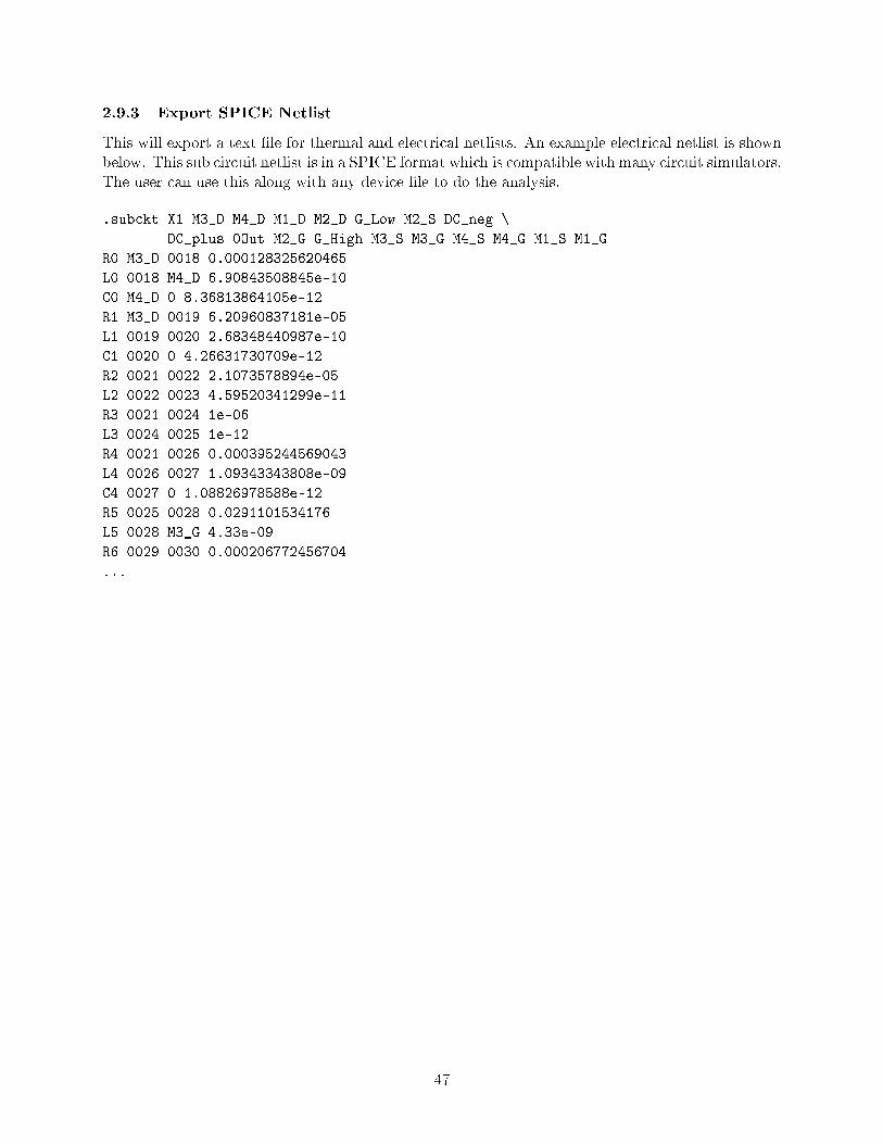
2.9.3 Export SPICE Netlist
This will export a text �le for thermal and electrical netlists. An example electrical netlist is shownbelow. This sub circuit netlist is in a SPICE format which is compatible with many circuit simulators.The user can use this along with any device �le to do the analysis.
.subckt X1 M3_D M4_D M1_D M2_D G_Low M2_S DC_neg \
DC_plus 0Out M2_G G_High M3_S M3_G M4_S M4_G M1_S M1_G
R0 M3_D 0018 0.000128325620465
L0 0018 M4_D 6.90843508845e-10
C0 M4_D 0 8.36813864105e-12
R1 M3_D 0019 6.20960837181e-05
L1 0019 0020 2.68348440987e-10
C1 0020 0 4.26631730709e-12
R2 0021 0022 2.1073578894e-05
L2 0022 0023 4.59520341299e-11
R3 0021 0024 1e-06
L3 0024 0025 1e-12
R4 0021 0026 0.000395244569043
L4 0026 0027 1.09343343808e-09
C4 0027 0 1.08826978588e-12
R5 0025 0028 0.0291101534176
L5 0028 M3_G 4.33e-09
R6 0029 0030 0.000206772456704
...
47
2.9.4 Export to Keysight EMPro
Please see the appendix for more detail.
3 Libraries and Editors
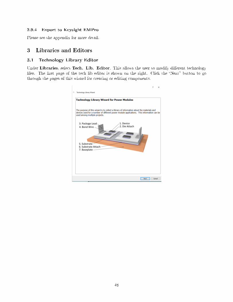
3.1 Technology Library Editor
Under Libraries, select Tech. Lib. Editor. This allows the user to modify di�erent technology�les. The �rst page of the tech lib editor is shown on the right. Click the �Next� button to gothrough the pages of this wizard for creating or editing components.
48

3.1.1 Device Information
This page allows the user to input device information. This includes the dimension and materialproperties as well as the landing position for bondwires. The user can also input the Verilog A�le for transistor/diode, while this information is not used in the optimization process, it will beincluded once the user exports the electrical netlist for a selected layout.
Click the �Save� button to save the new device to the library.
3.1.2 Add Die Attach
This page allows the user to assign the material properties for the die attach.Click the �Save� button to save the new die attach �le to the library.
49

3.1.3 Add Lead
This page allows the user to assign the material properties and dimensions for di�erent lead types.In PowerSynth, this currently falls into two categories: �Round� and �Bus Bar leads.�
Click the �Save� button to save the new lead �le to the library.
3.1.4 Add BondWire
This page allows the user to input dimensions and material properties for di�erent bondwire types.The bondwire model is based on JDEC standards.
Click the �Save� button to save the new bondwire �le to the library.
50

3.1.5 Add Substrate
This page allows the user to input dimensions and material properties for the metal and isolationlayers of DBC or DBA substrates.
Click the �Save� button to save the new �le to the library.
3.1.6 Add Substrate Attach
This allows the user to assign the material properties for the substrate attach.Click the �Save� button to save the new substrate attach �le to the library.
51

3.1.7 Add Baseplate
This allows the user to assign the material properties and dimensions for the baseplate.Click the �Save� button to save the new baseplate �le to the library.
52
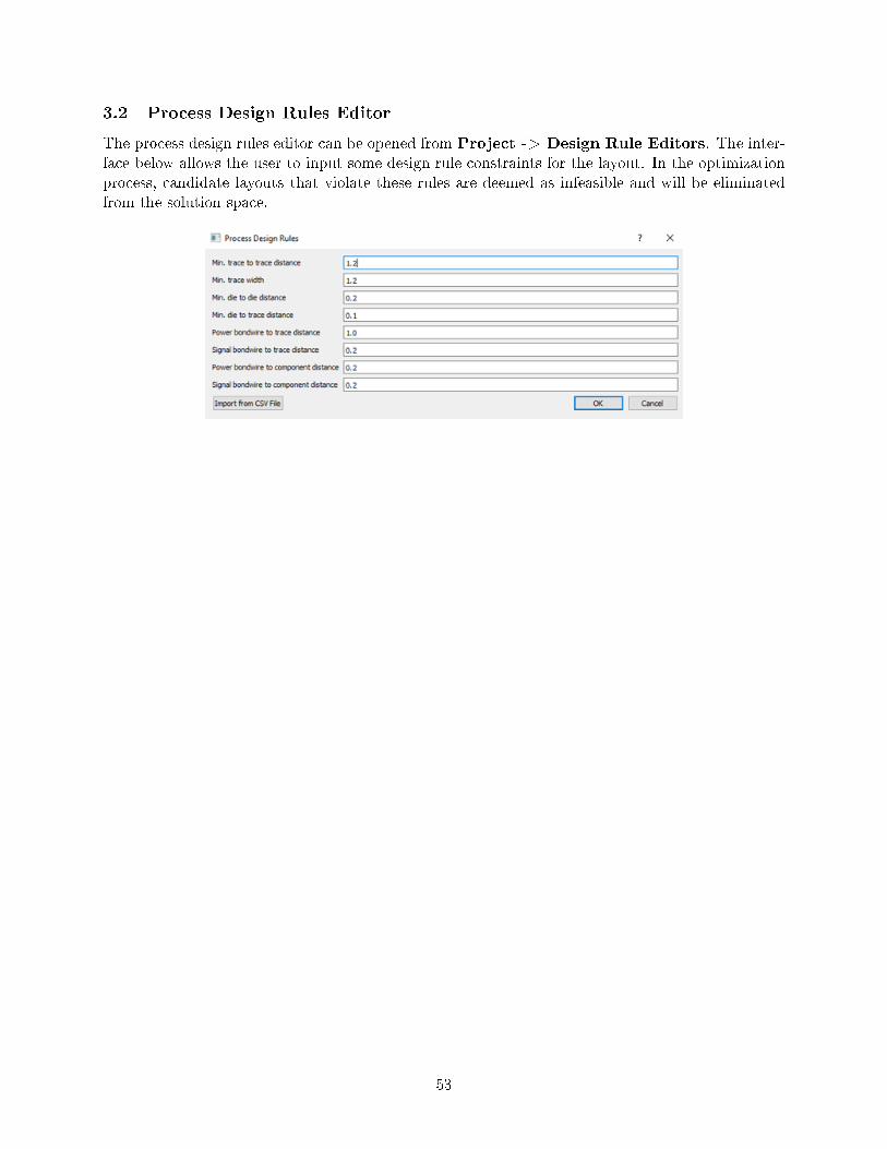
3.2 Process Design Rules Editor
The process design rules editor can be opened from Project -> Design Rule Editors. The inter-face below allows the user to input some design rule constraints for the layout. In the optimizationprocess, candidate layouts that violate these rules are deemed as infeasible and will be eliminatedfrom the solution space.
53
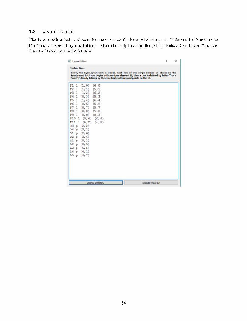
3.3 Layout Editor
The layout editor below allows the user to modify the symbolic layout. This can be found underProject-> Open Layout Editor. After the script is modi�ed, click �Reload SymLayout� to loadthe new layout to the workspace.
54
4 PowerSynth-Related Publications
This section contains a list of all the current publications related to PowerSynth as of the date ofthis document.
1. P. Tucker, "SPICE netlist generation for electrical parasitic modeling of multi-chip powermodule designs," 2013.
2. B. W. Shook, A. Nizam, Z. Gong, A. M. Francis and H. A. Mantooth, "Multi-objective lay-out optimization for multi-chip power modules considering electrical parasitics and thermalperformance," in Control and Modeling for Power Electronics (COMPEL), 2013 IEEE 14th
Workshop on, 2013.
3. B. W. Shook, Z. Gong, Y. Feng, A. M. Francis and H. A. Mantooth, "Multi-chip power modulefast thermal modeling for layout optimization," Computer-Aided Design and Applications, vol.9, pp. 837-846, 2012.
4. B. W. Shook, "The Design and Implementation of a Multi-Chip Power Module Layout Syn-thesis Tool," 2014.
5. J. Main, "A Manufacturer Design Kit for Multi-Chip Power Module Layout Synthesis," 2017.
6. Q. Le, T. Evans, S. Mukherjee, Y. Peng, T. Vrotsos and H. A. Mantooth, "Response surfacemodeling for parasitic extraction for multi-objective optimization of multi-chip power modules(MCPMs)," in Wide Bandgap Power Devices and Applications (WiPDA), 2017 IEEE 5th
Workshop on, 2017.
7. Q. Le, S. Mukherjee, T. Vrotsos and H. A. Mantooth, "Fast transient thermal and powerdissipation modeling for multi-chip power modules: A preliminary assessment of di�erentelectro-thermal evaluation methods," in Control and Modeling for Power Electronics (COM-
PEL), 2016 IEEE 17th Workshop on, 2016.
8. Z. Gong, "Thermal and electrical parasitic modeling for multi-chip power module layout syn-thesis," 2012.
9. T. M. Evans, Q. Le, S. Mukherjee, I. Al-Razi, T. Vrotsos, Y. Peng and H. A. Mantooth, "Pow-erSynth: A Module Layout Generation Tool," in IEEE Transactions on Power Electronics, vol34. no 6, pp. 5063-5078, June 2019, doi: 10.1109/TPEL.2018.2870346. Highlighted Article.
10. S. Mukherjee et al, "Toward Partial Discharge Reduction by Corner Correction in PowerModule Layouts," in Control and Modeling for Power Electronics (COMPEL), 2018.
11. I. Al Razi et al, "Constraint-Aware Algorithms for Heterogeneous Power Module Layout Syn-thesis and Reliability Optimization," in in Wide Bandgap Power Devices and Applications
(WiPDA), 2018 IEEE 6th Workshop on, 2018.
12. T. M. Evans, S. Mukherjee, Y. Peng and H. A. Mantooth, "Electronic Design Automation(EDA) Tools and Considerations for Electro-Thermo-Mechanical Co-Design of High VoltagePower Modules," 2020 IEEE Energy Conversion Congress and Exposition (ECCE), Detroit,MI, USA, 2020, pp. 5046-5052, doi: 10.1109/ECCE44975.2020.9235818.
55
5 Appendix 1: EMPro Export
5.1 Introduction
The EMPRo Export feature in PowerSynth allows a user to export designs generated by Power-Synth for further analysis in Keysight's EMPro and ADS. This document presents an overview ofthe capabilities available after export as well as the process in doing so. Furhtermore, while thisdocument provides a walkthrough of some of the key points for usage, it is assumed that the user isfamiliar with Keysight EMPro and ADS.
5.1.1 Functionality
This feature of PowerSynth takes a layout design from PowerSynth and generates a script to be runin EMPro. This script automatically de�nes the simulation type and frequency range, draws all ofthe design components and assigns materials, and sets up all of the requisite ports for simulation.
Exporting a design generated by PowerSynth to EMPro grants the user several cababilities forfuther analysis of a given design. These include, but are not limited to:
� S-Parameter modeling of a design
� Near and far �eld visualization
� Export to ADS for:
� Incorporation of Verilog-A device models
� Transient switching analysis
� Conducted EMI analysis
� Near �eld visualization of transient results
5.1.2 Caveats and Limitations in Current Release
Currently PowerSynth assumes a module buildup consisting of:
� Heat spreader
� Substrate attatch
� DBC-type substrate (Cu-ceramic-Cu)
� Die attatch
� Device
� Wire bonds
This stackup is �xed in the current release and so the resulting model in EMPro re�ects this.However, future versions of the tool will allow greater �exibility.
During the export, the thin attatchment layers are neglected to allow for easier meshing. Ad-ditionally, devices are not physically modeled. Instead, pads corresponding to those of the devicesare inserted and wire bonds are connected to them. This is done so that only the parasitics of themodule are extracted. Later, in circuit simulators such as ADS, the user can insert a device modelof their choosing into the corresponding ports inside the extracted layout parasitics model.
56
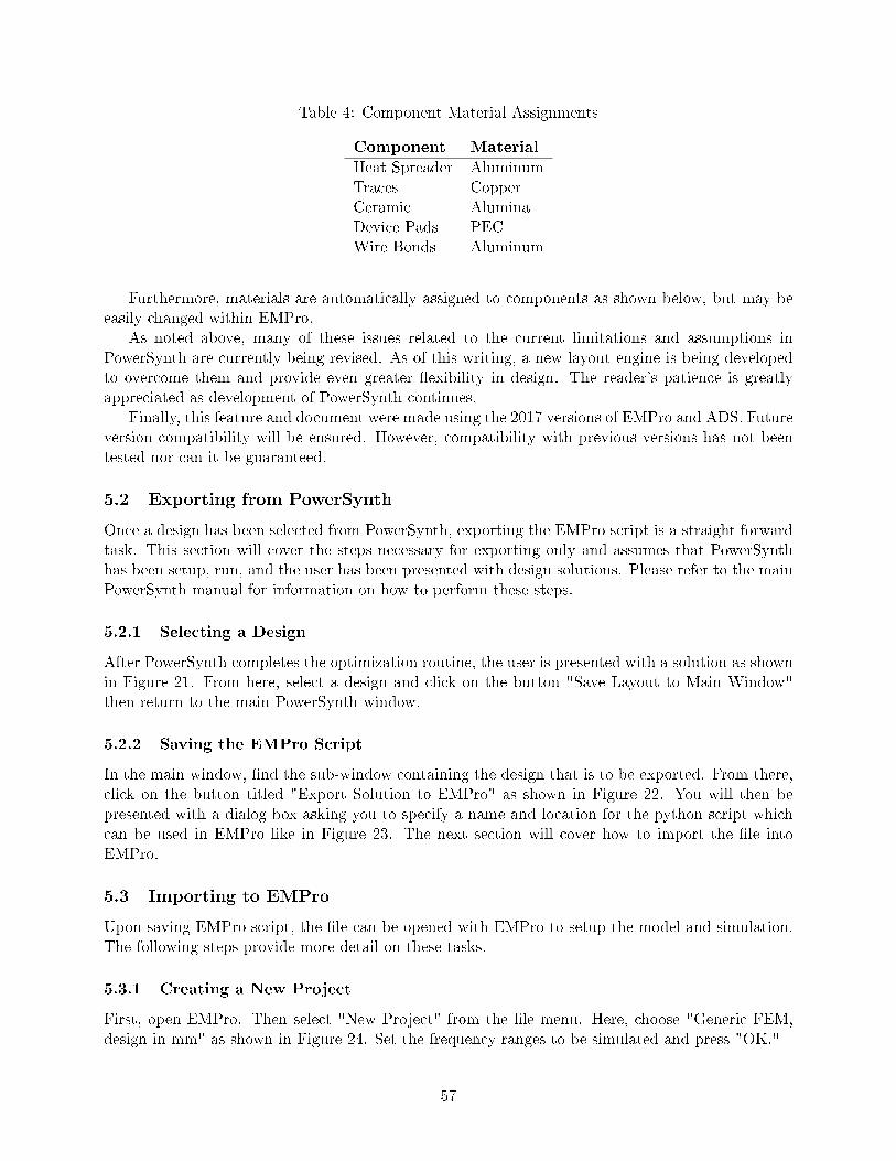
Table 4: Component Material Assignments
Component Material
Heat Spreader AluminumTraces CopperCeramic AluminaDevice Pads PECWire Bonds Aluminum
Furthermore, materials are automatically assigned to components as shown below, but may beeasily changed within EMPro.
As noted above, many of these issues related to the current limitations and assumptions inPowerSynth are currently being revised. As of this writing, a new layout engine is being developedto overcome them and provide even greater �exibility in design. The reader's patience is greatlyappreciated as development of PowerSynth continues.
Finally, this feature and document were made using the 2017 versions of EMPro and ADS. Futureversion compatibility will be ensured. However, compatibility with previous versions has not beentested nor can it be guaranteed.
5.2 Exporting from PowerSynth
Once a design has been selected from PowerSynth, exporting the EMPro script is a straight forwardtask. This section will cover the steps necessary for exporting only and assumes that PowerSynthhas been setup, run, and the user has been presented with design solutions. Please refer to the mainPowerSynth manual for information on how to perform these steps.
5.2.1 Selecting a Design
After PowerSynth completes the optimization routine, the user is presented with a solution as shownin Figure 21. From here, select a design and click on the button "Save Layout to Main Window"then return to the main PowerSynth window.
5.2.2 Saving the EMPro Script
In the main window, �nd the sub-window containing the design that is to be exported. From there,click on the button titled "Export Solution to EMPro" as shown in Figure 22. You will then bepresented with a dialog box asking you to specify a name and location for the python script whichcan be used in EMPro like in Figure 23. The next section will cover how to import the �le intoEMPro.
5.3 Importing to EMPro
Upon saving EMPro script, the �le can be opened with EMPro to setup the model and simulation.The following steps provide more detail on these tasks.
5.3.1 Creating a New Project
First, open EMPro. Then select "New Project" from the �le menu. Here, choose "Generic FEM,design in mm" as shown in Figure 24. Set the frequency ranges to be simulated and press "OK."
57
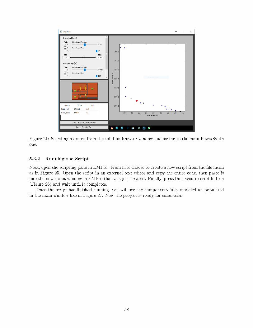
Figure 21: Selecting a design from the solution browser window and saving to the main PowerSynthone.
5.3.2 Running the Script
Next, open the scripting pane in EMPro. From here choose to create a new script from the �le menuas in Figure 25. Open the script in an external text editor and copy the entire code, then paste itinto the new script window in EMPro that was just created. Finally, press the execute script button(Figure 26) and wait until it completes.
Once the script has �nished running, you will see the components fully modeled an populatedin the main window like in Figure 27. Now the project is ready for simulation.
58
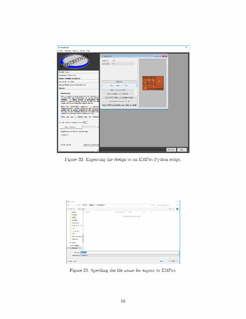
Figure 22: Exporting the design to an EMPro Python script.
Figure 23: Speci�ng the �le name for export to EMPro.
59
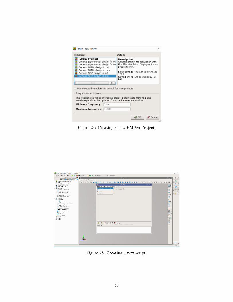
Figure 24: Creating a new EMPro Project.
Figure 25: Creating a new script.
60
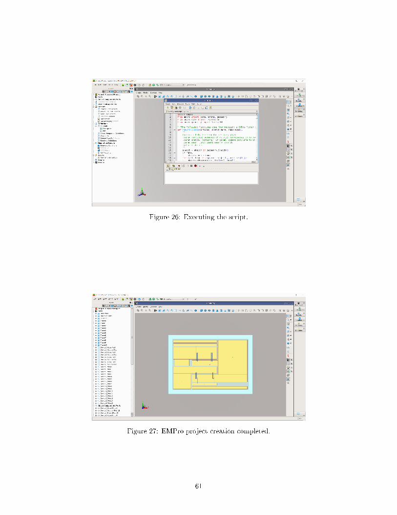
Figure 26: Executing the script.
Figure 27: EMPro project creation completed.
61