Embed Size (px)
Citation preview

Mixed-Signal Computer-Aided Deisgn (MSCAD) LaboratoryEnergy-Efficient Electronics and Design Automation (E3DA) Laboratory
PowerSynth User ManualVersion 1.9
Contents
1 Introduction 21.1 Executive Summary . . . . . . . . . . . . . . . . . . . . . . . . . . . . . . . . . . . . 2
1.1.1 PowerSynth Introduction . . . . . . . . . . . . . . . . . . . . . . . . . . . . . 21.1.2 About Version 1.9 . . . . . . . . . . . . . . . . . . . . . . . . . . . . . . . . . 2
1.2 Organization . . . . . . . . . . . . . . . . . . . . . . . . . . . . . . . . . . . . . . . . 21.3 PowerSynth v1.9 Architecture . . . . . . . . . . . . . . . . . . . . . . . . . . . . . . . 3
1.3.1 Manufacturer Design Kit (MDK) . . . . . . . . . . . . . . . . . . . . . . . . . 31.3.2 Hierarchical Constraint-Aware Layout Engine . . . . . . . . . . . . . . . . . . 31.3.3 Performance Evaluation Models . . . . . . . . . . . . . . . . . . . . . . . . . . 51.3.4 Optimization Algorithm . . . . . . . . . . . . . . . . . . . . . . . . . . . . . . 51.3.5 Post-Optimization and Solution Export . . . . . . . . . . . . . . . . . . . . . 6
2 Using PowerSynth v1.9 62.1 Installing and Running PowerSynth v1.9 . . . . . . . . . . . . . . . . . . . . . . . . . 62.2 Requirements . . . . . . . . . . . . . . . . . . . . . . . . . . . . . . . . . . . . . . . . 6
2.2.1 Technology Library Content . . . . . . . . . . . . . . . . . . . . . . . . . . . . 62.2.2 Initial Layout Description . . . . . . . . . . . . . . . . . . . . . . . . . . . . . 11
2.3 Macro Script Content . . . . . . . . . . . . . . . . . . . . . . . . . . . . . . . . . . . 152.3.1 Input Scripts . . . . . . . . . . . . . . . . . . . . . . . . . . . . . . . . . . . . 152.3.2 Layout Generation and Optimization Setup . . . . . . . . . . . . . . . . . . . 16
2.4 Folder Organization . . . . . . . . . . . . . . . . . . . . . . . . . . . . . . . . . . . . 192.5 Walk-Through an Example . . . . . . . . . . . . . . . . . . . . . . . . . . . . . . . . 21
3 PowerSynth-Related Publications 293.1 Useful Links . . . . . . . . . . . . . . . . . . . . . . . . . . . . . . . . . . . . . . . . . 30
4 Authors 314.1 Graduate Research Assistants . . . . . . . . . . . . . . . . . . . . . . . . . . . . . . . 314.2 Supervisors . . . . . . . . . . . . . . . . . . . . . . . . . . . . . . . . . . . . . . . . . 31
1

1 Introduction
1.1 Executive Summary
1.1.1 PowerSynth Introduction
PowerSynth is an electronic design automation (EDA) tool that can synthesize and optimize multi-chip power module (MCPM) layouts with significantly faster than any commercial tools. PowerSynthcurrently performs multi-objective optimization to produce Pareto-front solutions to the properplacement of power semiconductor device die and the routing of metal traces on ceramic substrates.The tool accounts for temperature distributions and electrical parasitics as a function of the layoutgeometries that it considers. This tool has been hardware-validated. Continued research on thisproject will further elaborate the capabilities by extending the work to greater fidelity in thermal,electrical, and mechanical domains.
1.1.2 About Version 1.9
As a part of PowerSynth continuous research and development, this version (v1.9) offers a commandline interface to the users with a significant improvement in layout representation and generationmethodology. Some of the major features in this version include:
• Generic layout representation technique for complex (2D/2.5D) geometry handling.
• Hierarchical constraint-aware, generic, efficient, and scalable layout generation methodology.
• Heretogeneous components handling.
• Rigid and flexible bonding wire connections.
• Voltage-current dependent reliability constraints handling.
• Arbitrary number of passive layers in the layer stack.
• Initial(single) layout performance evaluation.
• Partial element equivalent circuit (PEEC) based electrical model.
• Hardware-validated, fast, and accurate thermal model.
It is recommended that the user reads the manual of the previous version (v1.4) to have a betterunderstanding of the feature-wise differences in between this and the old version. The previous ver-sions of PowerSynth had graphical user interface (GUI) and some features like 3D solution browser,export to 3D modeling and FEA tools, and these features will be added back in our upcoming release(v2.0) with 3D MCPM layout optimization capability.
1.2 Organization
After a brief introduction to PowerSynth v1.9 architecture, this document introduces the commandline workflow. This document will show the user how to prepare the necessary files, and parametersfor using this version. Then, this document walks the user through the steps to optimize a sample2D half-bridge power module.
2
Python/Matlab API
External Models & Tools
Post-Optimization & Solution Browser
Complete
Solution Space
High E-Field
Filleting
Export Functions
Thermal
Parasitics
EMI
Static Thermal
Transient Thermal
Stress
Reliability
Manufacturer Design Kit (MDK)
Layout Geometry Script
Q3D
SolidWorks
SPICE
EMPro
Corner-Stitch Constraint Graph
Hierarchical Layout Generation Algorithms
Hierarchical Layout Engine
Models & Optimization Algorithms
Electrical Mechanical
Design
Pareto-Front
Input/Output Computationl Core
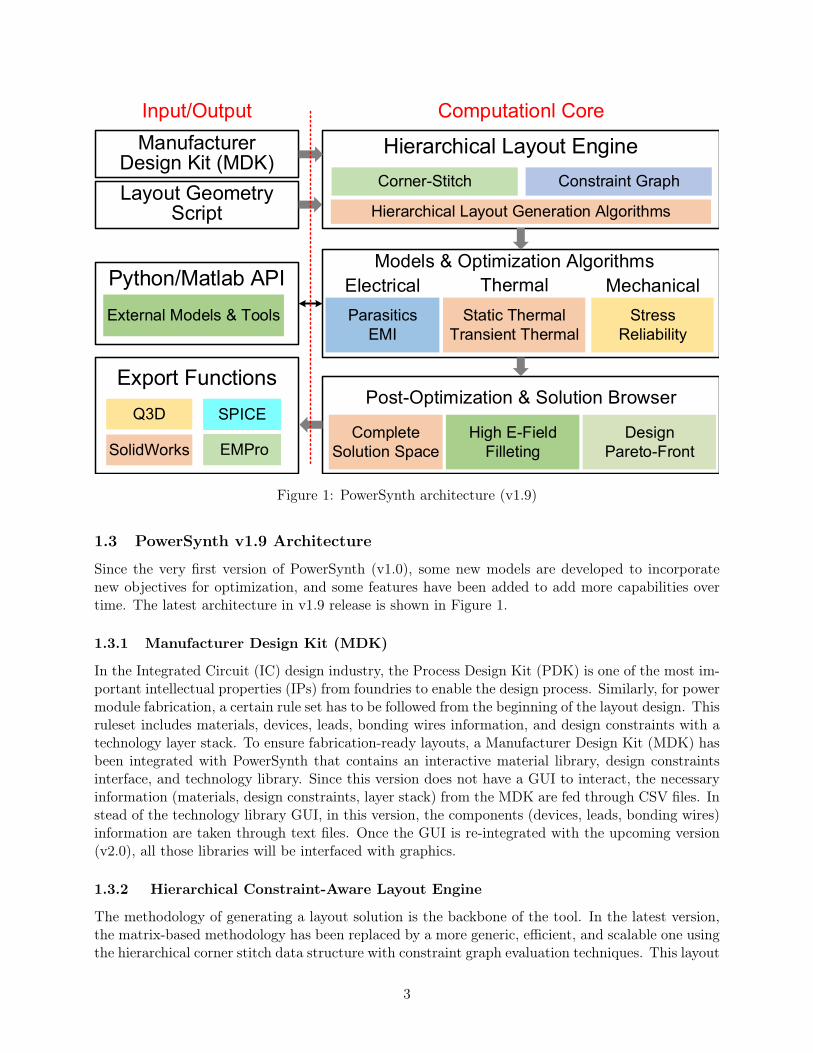
Figure 1: PowerSynth architecture (v1.9)
1.3 PowerSynth v1.9 Architecture
Since the very first version of PowerSynth (v1.0), some new models are developed to incorporatenew objectives for optimization, and some features have been added to add more capabilities overtime. The latest architecture in v1.9 release is shown in Figure 1.
1.3.1 Manufacturer Design Kit (MDK)
In the Integrated Circuit (IC) design industry, the Process Design Kit (PDK) is one of the most im-portant intellectual properties (IPs) from foundries to enable the design process. Similarly, for powermodule fabrication, a certain rule set has to be followed from the beginning of the layout design. Thisruleset includes materials, devices, leads, bonding wires information, and design constraints with atechnology layer stack. To ensure fabrication-ready layouts, a Manufacturer Design Kit (MDK) hasbeen integrated with PowerSynth that contains an interactive material library, design constraintsinterface, and technology library. Since this version does not have a GUI to interact, the necessaryinformation (materials, design constraints, layer stack) from the MDK are fed through CSV files. Instead of the technology library GUI, in this version, the components (devices, leads, bonding wires)information are taken through text files. Once the GUI is re-integrated with the upcoming version(v2.0), all those libraries will be interfaced with graphics.
1.3.2 Hierarchical Constraint-Aware Layout Engine
The methodology of generating a layout solution is the backbone of the tool. In the latest version,the matrix-based methodology has been replaced by a more generic, efficient, and scalable one usingthe hierarchical corner stitch data structure with constraint graph evaluation techniques. This layout
3

engine takes design constraints from the MDK together with an initial geometry script from the useras input to process the layout. With this methodology, an arbitrary number of components can behandled by applying generic and time-efficient algorithms. The significant improvements with thehierarchical constraint-aware layout engine are:
• An interactive constraint input feature which is helpful for user to specify or modify designconstraint values to have different layout structures.
• Three types of layout generation capability: minimum-sized layout, variable floorplan sized,and fixed floorplan sized.
• As the engine takes into account of all design constraints in the layout generation phase, italways generates 100% manufacture-able solutions.
• The updated layout engine can incorporate different types of optimization algorithms (i.e.,genetic algorithm, gradient-based approach, stochastic approach, randomization)
• This layout engine treats each component as rectangle, so geometrical complexity is not aproblem.
• This engine can process broader range of layouts even considering heterogeneous components(e.g. gate drivers, EMI filters, sensors, etc.).
• As the updated layout engine is constraint-aware, different types of constraints can be declared :design constraints, reliability constraints, user-defined constraints. Generated solutions alwayssatisfy all the given constraints.
MethodologyFrom the user-defined initial input script, using corner stitch data structure (used in Magic VLSItool), a collection of rectangular tiles are stored in a hierarchical tree structure. Based on designconstraints, constraint graphs (popular in VLSI floorplan compaction) are created for each corner-stitched plane. Two types of constraint graphs are consdiered: horizontal constraint graph (HCG)and vertical constraint graph (VCG) for maintaining horizontal and vertical relationship amongcomponents. These constraints are evaluated using the longest path algorithm and the results arepropagated through the tree. Bottom-up constraint propagation and top-down location propagationalgorithms are implemented to generate solution. Detail algorithms can be found in [13]. Someconcepts associated with layout generation are described as follows:
• Constraints: Two types of constraints are considered: (a) design constraints, (b) reliabilityconstraints.
(a) Design Constraints: These are standard design rules from the manufacturer. Threetypes of design constraints are considered.
1. Dimension Constraints: Here, minimum width along x-axis (Min Width), minimumwidth along y-axis (Min Height) and minimum enclosure (Min Enclosure) are specifiedfor each type of component.
2. Spacing Constraints: In this table, minimum spacing values between every pair ofcomponents are declared.
3. Enclosure Constraints: When a component is placed on top of another component,there may be some minimum enclosure value. So, this table has all possible minimumenclosure values.
4

(b) Reliability Constraints: These constraints are user-defined based on the high-voltage-current applications. To minimize partial discharge phenomena, and increase the reliability ofthe power module, user can define voltage-dependent minimum spacing and current-dependentminimum width constraints.
• Operating Modes: Based on the evaluation of the constraint graphs, there are three modesof operation (shown in Table 1).
Table 1: Summary of operating modes
Mode Purpose Evaluation Methodology0 Minimum sized layout Minimum constraint values
1 Variable floorplan layouts All weights are randomized with minimum constraints.No maximum constraints
2 Fixed floorplan layouts All weights are randomized with minimum constraints.Some have maximum constraints
– Minimum Size Layout: This layout is generated using all minimum constraint values.So, this layout reflects maximum possible power density for a layout. As this is theminimum sized solution, it is electrically optimized but thermal performance is so poor.
– Variable Size Layout: If this mode is selected, all constraint values are randomizedand new layout solution is generated. User can generate arbitrary number of valid layoutsolutions with different floorplan size.
– Fixed Size Layout: All edge weights are randomized within given area to generatearbitrary number of solutions. As floorplan size is always fixed there is less variation inthis mode than the previous one.
1.3.3 Performance Evaluation Models
The electrical model has been updated to consider both self and mutual inductance, resistance, andcapacitance. This is a PEEC-based model, which uses adaptive meshing and calculates parasiticsmore accurately than the previous response surface model. This model is described in [12]. Thelatest PowerSynth architecture is based on a modular approach so that the optimizer is flexiblein accepting various models through application programming interfaces (APIs) while evaluatingperformance metrics. For example, the Army Research Lab (ARL) has developed a 3D thermaland stress evaluation tool called ParaPower. To incorporate their thermal and stress model, aPowerSynth-ParaPower API has been developed to allow PowerSynth to use ParaPower for thermaland stress evaluations. However, in this version, this model has not been incorporated as thePowerSynth fast thermal model (described in [11]) is accurate and faster for any 2D/2.5D module.The ParaPower stress and thermal model, and another SPICE-based transient thermal model willbe incorporated in the next release.
1.3.4 Optimization Algorithm
In this version, the built-in solution generator algorithm "Non-guided randomization"([10]) has beenprovided as an optimization algorithm. Though this algorithm does not account for any specificobjective, this can generate a larger solution space than the genetic algorithm, which can eventuallyfind a better solution. The genetic algorithm implementation is on-going and will be incorporatedin the upcoming release.
5

1.3.5 Post-Optimization and Solution Export
In this version, along with the Pareto-front solutions, an entire solution space is also reportedafter optimization. Moreover, for each solution, the layout geometry is also exposed in a CSV filecontaining each component’s coordinates, width, and length. This information helps a designer toregenerate the geometry script for the solution layout. Though the automatic export to commercialFEA tools like ANSYS Q3D, and SolidWorks feature is disabled in this command line version, itwill be back with the next release GUI version.
2 Using PowerSynth v1.9
2.1 Installing and Running PowerSynth v1.9
To install PowerSynth v1.9, run the PowerSynth install wizard. It will take some time to install.Upon installation, the user can run PowerSynth v1.9 executable.Note: It is STRONGLY RECOMMENDED that you install PowerSynth in the C drive (the de-fault installation directory) and NOT in Program Files. Installing PowerSynth in Program Files canresult in various issues relating to administrator permissions.To run the commandline version, the steps are as follows:1. Start a command prompt as administrator.2. Go to the directory of "PowerSynth.exe".3. Run PowerSynth by entering the command: PowerSynth.exe.4. The command prompt will ask for the location of the "Settings.info" file. This file is alreadyprovided with the package.5. Upon entering the location of the "Settings.info" file, hit enter.6. Now, it will ask for the "Macro script" file location.7. Sample "Macro script" is provided in the "Sample_Projects" folder inside the package. Youcan use any of the test case macro script file location to test it or you can create your own test case.Details of preparing a "Macro script" are described in Section 2.2.8. Upon entering the "Macro script" file location, PowerSynth will execute necessary steps ac-cording to the option specified in the "Macro script".
So, to run PowerSynth v1.9, user needs to files: (a) Settings file, and (b) Macro script. Sincethe Settings file is provided with the package, the user needs to create a Macro script only torun a layout optimization. So, in the following subsections, the Macro script prepartion detailsare described.
2.2 Requirements
2.2.1 Technology Library Content
To design a standard 2D/2.5D power module (shown in Figure 2), the key elements are as follows:1. Baseplate2. Substrate (Direct Bonded Copper (DBC): Back-side metal, Ceramic, Top-side metal)3. Components (Devices: MOSFETs, Diodes, IGBTs, Capacitors, etc.)4. Connectors (Leads: power and signal)5. Bonding wires.
Since the technology library is not integrated with this version, these elements information aretaken through files. The files associated with these elements are as follows:
6
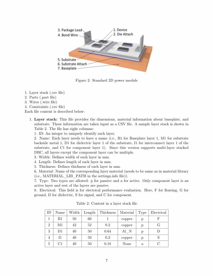
Figure 2: Standard 2D power module
1. Layer stack (.csv file)2. Parts (.part file)3. Wires (.wire file)4. Constraints (.csv file)Each file content is described below:
1. Layer stack: This file provides the dimensions, material information about baseplate, andsubstrate. These information are taken input as a CSV file. A sample layer stack is shown inTable 2. The file has eight columns:1. ID: An integer to uniquely identify each layer.2. Name: Each layer needs to have a name (i.e., B1 for Baseplate layer 1, M1 for substratebackside metal 1, D1 for dielectric layer 1 of the substrate, I1 for interconnect layer 1 of thesubstrate, and C1 for component layer 1). Since this version supports multi-layer stackedDBC, all layers except the component layer can be multiple.3. Width: Defines width of each layer in mm.4. Length: Defines length of each layer in mm.5. Thickness: Defines thickness of each layer in mm.6. Material: Name of the corresponding layer material (needs to be same as in material library(i.e., MATERIAL_LIB_PATH in the settings.info file)).7. Type: Two types are allowed: p for passive and a for active. Only component layer is anactive layer and rest of the layers are passive.8. Electrical: This field is for electrical performance evaluation. Here, F for floating, G forground, D for dielectric, S for signal, and C for component.
Table 2: Content in a layer stack file
ID Name Width Length Thickness Material Type Electrical
1 B1 50 60 1 copper p F
2 M1 42 52 0.2 copper p G
3 D1 40 50 0.64 Al_N p D
4 I1 40 50 0.2 copper p S
5 C1 40 50 0.18 None a C
7
Since, this version supports only layer-based geometry, the component layer (ID=5 in Table 2)thickness and material information are optional.
2. Parts: The components (devices) and connectors (leads) are considered as parts in this version.The dimensions, material information of these elements are taken from corresponding .part file.These files are written in a text editor and saved as .part extension. A sample MOSFET.partand power_lead.part file content are shown in Figure 3 (a), (b), respectively.
Name CPM2-1200-0025B
Type component
Link
https://www.wolfspeed.com/downloads/dl/file/id/152/product/2/cpm2_1200_0025b.pdf
Footprint 4 6
Thickness 0.18
Material SiC
Pins Drain Source Gate
Drain 0 0 4 6 B
Source 0.335 0.35 3.5 4.5 T
Gate 1.03 5 0.5 0.5 T
Parasitics
Drain Source R:25e-3
Drain Gate R:1.1
Gate Source R:1.1
Name PL1
Type connector
Footprint 6 2
Thickness 2
(a) (b)
Figure 3: Content in (a) MOSFET.part, (b) power_lead.part file
In Figure 3 (a), each row has a key name e.g. “Name” and a value separated by a space e.g.:“CPM2-1200-0025B”. The definition for each key is as follows:Name: Name of the PartType: There are 2 options: component (device like MOS, diode, capacitor, etc.) or connector(terminals like power lead, signal lead, etc.)Link: A link to the part datasheetFootprint: Width <space> Length (Provide the footprint of the component in mm)Thickness: Thickness of the component (in mm)Material: Name of the Material (e.g., SiC) [should match with material library from MDK(materials.csv file in MATERIAL_LIB_PATH of "settings.info" file.)]Pins [list of preferred pin names separated by space]: Provide a list of pin namesPin_name: For each pin provide a pin pad rectangle (bottom-left coordinate x <space> y<space> width <space> height) reference to the component bottom left corner. At the endof the pin rectangle add a keyword B or T to distinguish between Bottom and Top side pins.Parasitics: Used to provide component internal parasitic information.Pin_name1 <space> Pin_name2 <space> R: R_val <space> L:L_val <space> C:C_valProvide a list of RLC value between every 2 pins (with internal parasitics)
For different devices, the keys need to be same, but the values will be changed depending onthe device type. In Figure 3 (b), each row has a key, value pair separated by a space.Thedefinitions for each key are similar to those in Figure 3 (a).
In this version, the footprint dimensions declared in the .part files need to be always integer.However, the user can change the footprint dimensions into the floating point numbers in the
8
constraint file (described in the "Constraint File" section). Also, all .part files need to be savedin the "Part_Lib" folder. More sample .part files are provided in the "Sample_Projects" folderinside "Part_Lib".
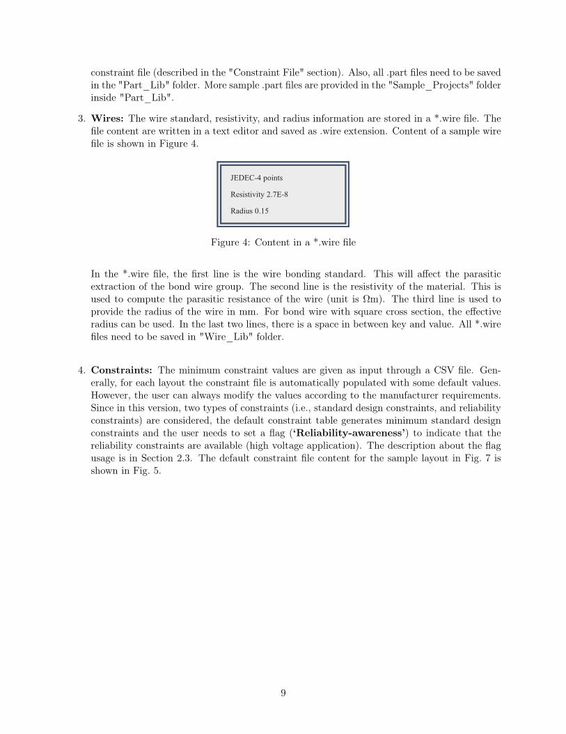
3. Wires: The wire standard, resistivity, and radius information are stored in a *.wire file. Thefile content are written in a text editor and saved as .wire extension. Content of a sample wirefile is shown in Figure 4.
JEDEC-4 points
Resistivity 2.7E-8
Radius 0.15
Figure 4: Content in a *.wire file
In the *.wire file, the first line is the wire bonding standard. This will affect the parasiticextraction of the bond wire group. The second line is the resistivity of the material. This isused to compute the parasitic resistance of the wire (unit is Ωm). The third line is used toprovide the radius of the wire in mm. For bond wire with square cross section, the effectiveradius can be used. In the last two lines, there is a space in between key and value. All *.wirefiles need to be saved in "Wire_Lib" folder.
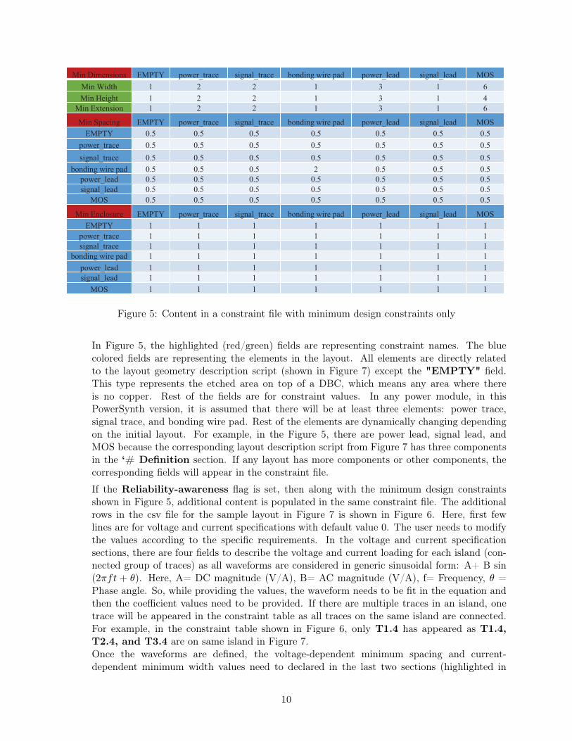
4. Constraints: The minimum constraint values are given as input through a CSV file. Gen-erally, for each layout the constraint file is automatically populated with some default values.However, the user can always modify the values according to the manufacturer requirements.Since in this version, two types of constraints (i.e., standard design constraints, and reliabilityconstraints) are considered, the default constraint table generates minimum standard designconstraints and the user needs to set a flag (‘Reliability-awareness’) to indicate that thereliability constraints are available (high voltage application). The description about the flagusage is in Section 2.3. The default constraint file content for the sample layout in Fig. 7 isshown in Fig. 5.
9
Min Dimensions EMPTY power_trace signal_trace bonding wire pad power_lead signal_lead MOS
Min Width 1 2 2 1 3 1 6
Min Height 1 2 2 1 3 1 4
Min Extension 1 2 2 1 3 1 6
Min Spacing EMPTY power_trace signal_trace bonding wire pad power_lead signal_lead MOS
EMPTY 0.5 0.5 0.5 0.5 0.5 0.5 0.5
power_trace 0.5 0.5 0.5 0.5 0.5 0.5 0.5
signal_trace 0.5 0.5 0.5 0.5 0.5 0.5 0.5
bonding wire pad 0.5 0.5 0.5 2 0.5 0.5 0.5
power_lead 0.5 0.5 0.5 0.5 0.5 0.5 0.5
signal_lead 0.5 0.5 0.5 0.5 0.5 0.5 0.5
MOS 0.5 0.5 0.5 0.5 0.5 0.5 0.5
Min Enclosure EMPTY power_trace signal_trace bonding wire pad power_lead signal_lead MOS
EMPTY 1 1 1 1 1 1 1
power_trace 1 1 1 1 1 1 1
signal_trace 1 1 1 1 1 1 1
bonding wire pad 1 1 1 1 1 1 1
power_lead 1 1 1 1 1 1 1
signal_lead 1 1 1 1 1 1 1
MOS 1 1 1 1 1 1 1
Figure 5: Content in a constraint file with minimum design constraints only
In Figure 5, the highlighted (red/green) fields are representing constraint names. The bluecolored fields are representing the elements in the layout. All elements are directly relatedto the layout geometry description script (shown in Figure 7) except the "EMPTY" field.This type represents the etched area on top of a DBC, which means any area where thereis no copper. Rest of the fields are for constraint values. In any power module, in thisPowerSynth version, it is assumed that there will be at least three elements: power trace,signal trace, and bonding wire pad. Rest of the elements are dynamically changing dependingon the initial layout. For example, in the Figure 5, there are power lead, signal lead, andMOS because the corresponding layout description script from Figure 7 has three componentsin the ‘# Definition section. If any layout has more components or other components, thecorresponding fields will appear in the constraint file.
If the Reliability-awareness flag is set, then along with the minimum design constraintsshown in Figure 5, additional content is populated in the same constraint file. The additionalrows in the csv file for the sample layout in Figure 7 is shown in Figure 6. Here, first fewlines are for voltage and current specifications with default value 0. The user needs to modifythe values according to the specific requirements. In the voltage and current specificationsections, there are four fields to describe the voltage and current loading for each island (con-nected group of traces) as all waveforms are considered in generic sinusoidal form: A+ B sin(2πft + θ). Here, A= DC magnitude (V/A), B= AC magnitude (V/A), f= Frequency, θ =Phase angle. So, while providing the values, the waveform needs to be fit in the equation andthen the coefficient values need to be provided. If there are multiple traces in an island, onetrace will be appeared in the constraint table as all traces on the same island are connected.For example, in the constraint table shown in Figure 6, only T1.4 has appeared as T1.4,T2.4, and T3.4 are on same island in Figure 7.Once the waveforms are defined, the voltage-dependent minimum spacing and current-dependent minimum width values need to declared in the last two sections (highlighted in
10
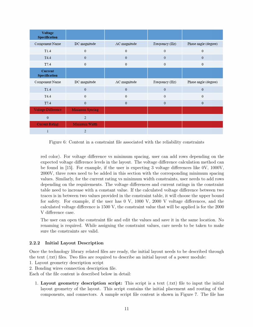
Figure 6: Content in a constraint file associated with the reliability constraints
red color). For voltage difference vs minimum spacing, user can add rows depending on theexpected voltage difference levels in the layout. The voltage difference calculation method canbe found in [15]. For example, if the user is expecting 3 voltage differences like 0V, 1000V,2000V, three rows need to be added in this section with the corresponding minimum spacingvalues. Similarly, for the current rating vs minimum width constraints, user needs to add rowsdepending on the requirements. The voltage differences and current ratings in the constrainttable need to increase with a constant value. If the calculated voltage difference between twotraces is in between two values provided in the constraint table, it will choose the upper boundfor safety. For example, if the user has 0 V, 1000 V, 2000 V voltage differences, and thecalculated voltage difference is 1500 V, the constraint value that will be applied is for the 2000V difference case.
The user can open the constraint file and edit the values and save it in the same location. Norenaming is required. While assigning the constraint values, care needs to be taken to makesure the constraints are valid.
2.2.2 Initial Layout Description
Once the technology library related files are ready, the initial layout needs to be described throughthe text (.txt) files. Two files are required to describe an initial layout of a power module:1. Layout geometry description script2. Bonding wires connection description file.Each of the file content is described below in detail:
1. Layout geometry description script: This script is a text (.txt) file to input the initiallayout geometry of the layout. This script contains the initial placement and routing of thecomponents, and connectors. A sample script file content is shown in Figure 7. The file has
11
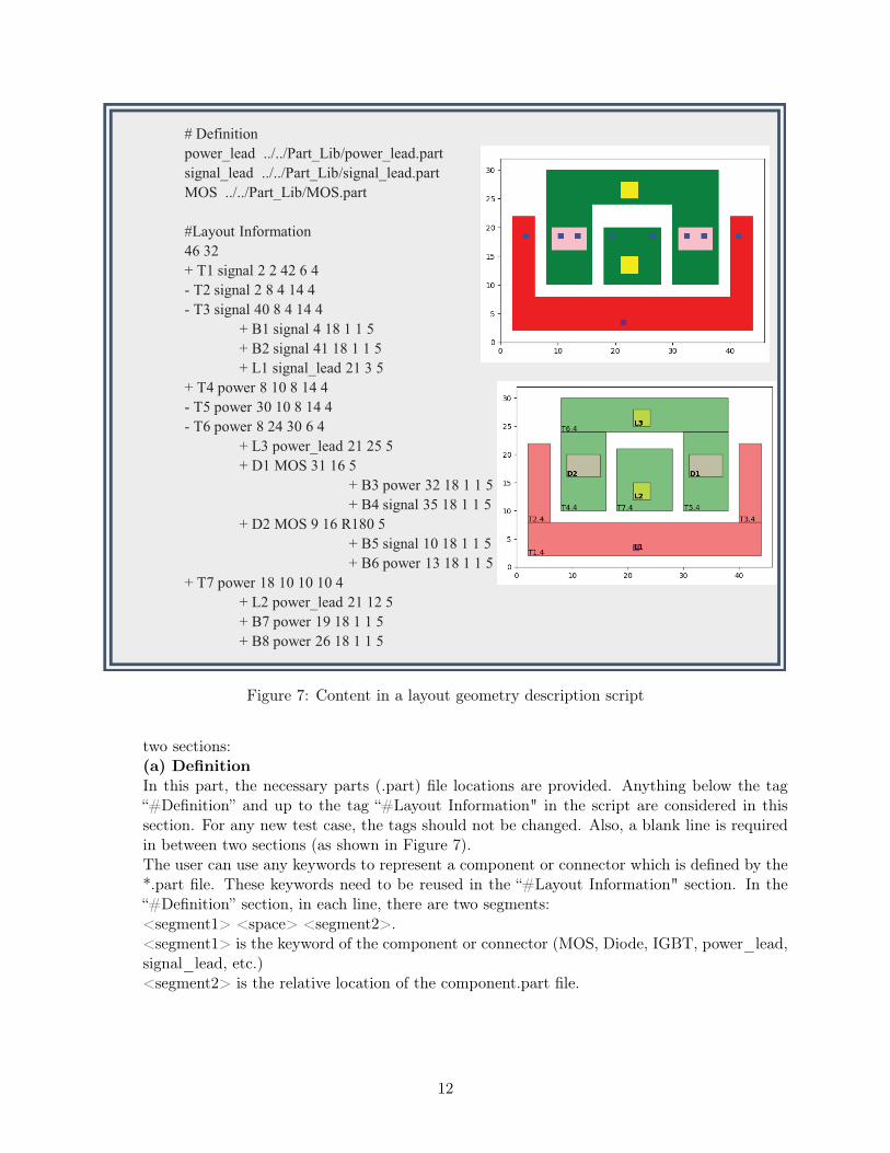
# Definition
power_lead ../../Part_Lib/power_lead.part
signal_lead ../../Part_Lib/signal_lead.part
MOS ../../Part_Lib/MOS.part
#Layout Information
46 32
+ T1 signal 2 2 42 6 4
- T2 signal 2 8 4 14 4
- T3 signal 40 8 4 14 4
+ B1 signal 4 18 1 1 5
+ B2 signal 41 18 1 1 5
+ L1 signal_lead 21 3 5
+ T4 power 8 10 8 14 4
- T5 power 30 10 8 14 4
- T6 power 8 24 30 6 4
+ L3 power_lead 21 25 5
+ D1 MOS 31 16 5
+ B3 power 32 18 1 1 5
+ B4 signal 35 18 1 1 5
+ D2 MOS 9 16 R180 5
+ B5 signal 10 18 1 1 5
+ B6 power 13 18 1 1 5
+ T7 power 18 10 10 10 4
+ L2 power_lead 21 12 5
+ B7 power 19 18 1 1 5
+ B8 power 26 18 1 1 5
Figure 7: Content in a layout geometry description script
two sections:(a) DefinitionIn this part, the necessary parts (.part) file locations are provided. Anything below the tag“#Definition” and up to the tag “#Layout Information" in the script are considered in thissection. For any new test case, the tags should not be changed. Also, a blank line is requiredin between two sections (as shown in Figure 7).The user can use any keywords to represent a component or connector which is defined by the*.part file. These keywords need to be reused in the “#Layout Information" section. In the“#Definition” section, in each line, there are two segments:<segment1> <space> <segment2>.<segment1> is the keyword of the component or connector (MOS, Diode, IGBT, power_lead,signal_lead, etc.)<segment2> is the relative location of the component.part file.
12

(b) Layout InformationThis section describes the layout geometry and component hierarchy information for the layoutengine. Anything below the tag “#Layout Information” are used to describe the layout geom-etry. The geometry should be described hierarchically and the hierarchical order is bottom-to-top. For example, in the sample script shown in Figure 7, T4, T5, T6 are connected traces andtogether create an island. This island should be declared first and then the devices or leadson top of it need to be declared. Each island can be composed of single or multiple traces.All connected traces in the same island needs to be declared at same hierarchy level. Thedeclaration should start with a ‘+’ character and other connected components need to startwith a ‘-‘ character. All components in each connected group should be of the same type (i.e.,power traces or signal traces).
Each hierarchy level is separated by a ‘tab’ in the script and we currently support up to 3levels of hierarchy (2 tabs) in this version (Trace->Device->Pin). Also, in the input script, thecoordinates should be given as integer values. However, in the constraint table, the fractionalconstraint value is allowed up to 3rd decimal point.
All of the width and height information for devices or leads are directly read from the corre-sponding “.part file” mentioned in the Definition section. So, these components do not havewidth or height information specified in the layout geometry description script, whereas others(e.g., traces and bond wire pads) have width and height fields.
To have a bond wire, the source pad and destination pad of the bond wire needs to be alignedaccording to the wire orientation. For example, in the sample script (shown in Figure 7),the gate signal is connected from B4 to B2 (Bonding wires connection description filesection). B4 is on top of the gate pad of D2. So, B4 and B2 should have the same y coordinateas this represents a horizontal bond wire connection. The bond wire pad is always a squarewith size of 1 mm in the input script, even though it is considered as a point connection inthe algorithms.
Description of each line in the ’#Layout Information’ section:Line1: size of initial layout (width (along X-axis), height (along Y-axis))Line2-to-end: each line has several fields:For all routing paths (Traces, Bond wire pads) have 8 fields:1. ‘+/-’ : Connectivity definition character2. ‘ID’ : layout component id (T1: Trace 1, T2: Trace 2, B1: Bond wire pad 1,etc.)3. ‘type of component’: for traces, bond wire pads-> power or signal4. x coordinate: bottom left corner’s x coordinate5. y coordinate: bottom left corner’s y coordinate6. width: width of the rectangle (along x axis)7. height: height of the rectangle (along y axis)8. layer_id: id of the layer(value is taken from the layer stack)For all parts (Devices, Leads) have 6-7 fields:1. ‘+/-’ : Connectivity definition character2. ‘ID’ : layout component id (D1: Device 1, L1: Lead 1,etc.)3. ‘type of component’:for devices-> name (should match with definition part) (MOS,Diode, IGBT, etc.)for leads-> name of lead (power_lead or signal_lead or neutral_lead)4. x coordinate: bottom left corner’s x coordinate5. y coordinate: bottom left corner’s y coordinate6. Rotate angle: R90(90°rotation), R180(180°rotation), R270(270°rotation)
13
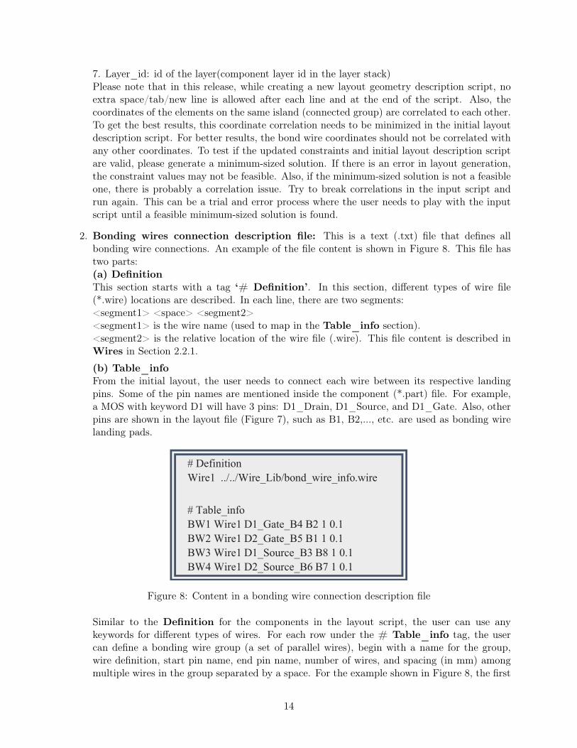
7. Layer_id: id of the layer(component layer id in the layer stack)Please note that in this release, while creating a new layout geometry description script, noextra space/tab/new line is allowed after each line and at the end of the script. Also, thecoordinates of the elements on the same island (connected group) are correlated to each other.To get the best results, this coordinate correlation needs to be minimized in the initial layoutdescription script. For better results, the bond wire coordinates should not be correlated withany other coordinates. To test if the updated constraints and initial layout description scriptare valid, please generate a minimum-sized solution. If there is an error in layout generation,the constraint values may not be feasible. Also, if the minimum-sized solution is not a feasibleone, there is probably a correlation issue. Try to break correlations in the input script andrun again. This can be a trial and error process where the user needs to play with the inputscript until a feasible minimum-sized solution is found.
2. Bonding wires connection description file: This is a text (.txt) file that defines allbonding wire connections. An example of the file content is shown in Figure 8. This file hastwo parts:(a) DefinitionThis section starts with a tag ‘# Definition’. In this section, different types of wire file(*.wire) locations are described. In each line, there are two segments:<segment1> <space> <segment2><segment1> is the wire name (used to map in the Table_info section).<segment2> is the relative location of the wire file (.wire). This file content is described inWires in Section 2.2.1.
(b) Table_infoFrom the initial layout, the user needs to connect each wire between its respective landingpins. Some of the pin names are mentioned inside the component (*.part) file. For example,a MOS with keyword D1 will have 3 pins: D1_Drain, D1_Source, and D1_Gate. Also, otherpins are shown in the layout file (Figure 7), such as B1, B2,..., etc. are used as bonding wirelanding pads.
# Definition
Wire1 ../../Wire_Lib/bond_wire_info.wire
# Table_info
BW1 Wire1 D1_Gate_B4 B2 1 0.1
BW2 Wire1 D2_Gate_B5 B1 1 0.1
BW3 Wire1 D1_Source_B3 B8 1 0.1
BW4 Wire1 D2_Source_B6 B7 1 0.1
Figure 8: Content in a bonding wire connection description file
Similar to the Definition for the components in the layout script, the user can use anykeywords for different types of wires. For each row under the # Table_info tag, the usercan define a bonding wire group (a set of parallel wires), begin with a name for the group,wire definition, start pin name, end pin name, number of wires, and spacing (in mm) amongmultiple wires in the group separated by a space. For the example shown in Figure 8, the first
14
line in the # Table_info section defines a bonding wire with name: ‘BW1’, type: ‘Wire1’,start pin: ‘D1_Gate_B4’, end pin: ‘B2’, number of wires: ‘1’, and spacing: ‘0.1’. Since B4and B2 are connected, in the layout script (shown in Figure 7) they have same Y-coordinateas this wire is a horizontal wire. Also, B4 represents the gate pin of the device D1, so the startpin name is ‘D1_Gate_B4’.
2.3 Macro Script Content
In a macro script there are two major sections:
1. Input Scripts
2. Layout Generation and Optimization Setup
Description about each section is as follows:
2.3.1 Input Scripts
In this section, eight files/directories locations are provided. Detailed description for each of themare provided below:
1. Layout_script: In this field, the relative location of the Layout geometry descriptionscript (described in Section 2.2.2) needs to be provided.
2. Bondwire_setup: Here, the relative location of the Bonding wires connection descrip-tion file (described in Section 2.2.2) needs to be provided.
3. Layer_stack: Relative location of the Layer stack file (described in Section 2.2.1) is pro-vided here.
4. Parasitic_model: In this version, only PEEC-model is embedded for electrical parasiticsextraction. Some sample files are given for the test cases in ’Sample_Projects’ folder withthe package. Please, note that for different layouts, if you experience very large or negativevalues during resistance and inductance extraction, a new model is needed. Please contact thedevelopers if you are getting weird parasitic values for your case as the interface of creating anew model file is not provided in this version.
5. Fig_dir: Needs a relative path of a directory to save the figures.
6. Solution_dir: Needs a relative path of a directory to save the solution database file. Thisdatabase file contains layout information which is used to plot the figures. In this folder, allperformance values of the solutions and corresponding Pareto-front solution set are reportedas a .csv format. Besides, two folders will be created, where each layout solution componentsand corresponding coordinates, dimensions of all solutions and Pareto solutions are dumpedin individual CSV file.
7. Constraint_file: The constraint file is a CSV file, where all constraint values are stored.Depending on the mode of the flag ‘New’ in the macro file (described in Section 2.3.2), aconstraint file will be created or loaded to generate the layout solutions. In this field, theuser needs to provide the relative location of an empty CSV file (for the first time for eachlayout) and make sure the ’New’ flag is set to 1. This flag value allows user to modify thedefault constraint values populated by PowerSynth. Once the values are modified, the ’New’flag needs to be set to 0, which reloads the constraint values in the specified file and does notrequire to edit the values again. The file content is described in Section 2.2.1.
15

8. Trace_Ori: This field is the ’Trace Orientation’ description file. A text (.txt) file relativelocation with trace orientations needs to be provided. This file is required for the electricalmodel to evaluate electrical performance. Two orientations are possible for each trace: Hori-zontal and Vertical. This represents the preferred current flow direction for the trace.The format for the file content is as follows:H: Horizontal trace_1 name.layer_id, Horizontal trace_2 name.layer_id, . . . . . . , etc.V: Vertical trace_1 name.layer_id, Vertical trace_2 name.layer_id, . . . . . . , etc.Here, layer_id is the last field in that trace geometry definition line in Layout_script.For example, the layout shown in Fig. 7, the Trace_Ori.txt file content is:H: T1.4,T6.4V: T2.4,T3.4,T4.4,T5.4,T7.4
2.3.2 Layout Generation and Optimization Setup
Layout GenerationIn this section, PowerSynth layout solution generation and performance evaluation setup are defined.PowerSynth v1.9 can serve three purposes:1. Layout solution generation only.2. Initial layout performance evaluation.3. Layout optimization: solution generation and performance evaluation.Each field for this section is described below:
1. Reliability-awareness: If high-voltage and current dependent constraints (reliability con-straints) are available and the user wants to apply those, this flag should be set to 2. Settingup this flag as 0 indicates no reliability constraints are applied. If this flag is set to 1, worst-caseconditions (theoretical, not always practical) are considered. To have reasonable, practical,and reliability-aware layout generation, this flag needs to be set to 2. If reliability-awarenessis set to 1, or 2, in the constraint table, voltage and current specifications are populated formodification. Details are described in Section 2.2.1.
2. New: If ‘New’ flag is set to 1, user will be asked to edit the constraint table in the givenconstraint file location while running the test case. Once the edition is done, user needs toenter "1" in the terminal to continue. For each new test case, this flag has to be set to 1 forthe first run. Then, for other iteartions, the flag needs to be set to 0, otherwise the modifiedconstraint values will be overwritten by the default values. If the flag is set to 0, the constraintvalues already saved in the given constraint file are used to generate solutions.
3. Plot_Solution: If this flag is set to 1, all solution layout images will be saved in the Fig_dir.This is only recommended for small solution spaces (<100 layouts). For large solution spaces,plotting each figure will cause memory issue in matplotlib. So, this flag should be set to 0.
4. Flexible_Wire: If this flag is set to 0, the bonding wires are rigid (i.e., needs to be strictlyhorizontal or vertical). In the Layout_script, any connected pair of bond wire pads needto be declared carefully to maintain their orientation alignment. For example, if the bondwire is horizontal, the start and end pins of the wire need to be horizontally aligned (samey coordinates). Also, in the Bondwire_setup file, the connection is allowed only betweenbond wire pads. If the flag is set to 1, flexible bond wires are considered. A flexible bond wireis one that can be connected between any two points in the layout. There is no restriction
16

on the orientation (i.e., horizontal, or vertical). In this case, the Layout_script and Bond-wire_setup file need to compatible with the flexible wire implementation. For flexible bondwires, in the layout script, no bond wire pad is allowed on top of the device. So, in the bondwire connection table, the wires having source or destination as a device, needs to be only pad(as declared in part definition). However, the flexible wire would overestimate the bondingwire length and so this feature is not available for the users. So, default value is set to 0 andit is recommended not to change the value. If you want to use this feature, please contactdevelopers.
5. Option: To choose from the three options mentioned earlier: 1. Layout solution generationonly, 2. Initial layout evaluation, 3. Layout optimization/evaluation, this flag is provided.Based on your choice provide 0, 1, 2 respectively for the options given above. For example: torun layout optimization, you will provide 2 in the option field. Initial layout does not guaranteedesign rule check (DRC) clean solution as it is described by the user. Other options generatesolutions by considering design conatraints and hence they are DRC-clean.
6. Layout_Mode: This field is related to layout generation. In this version, three modes oflayout generation are allowed: 1. Mode-0: minimum-sized solution, 2. Mode-1: variable-sizedsolutions, 3. Mode-2: fixed-sized solutions. Details are described in Section 1.3.2. This optionis effective if the user has chosen 0 or 2 as Option field value. For Mode-0, a single solutionis generated. For other modes user can choose number of solutions. Since in Mode-0, user cangenerate a single solution, if ‘Option’ is set to 2, that single solution will be evaluated andthis will not generate any Pareto-front as the solution space length is 1. It is recommendedthat for each new test case, user generates minimum-sized solution (Mode=0) to make surethat the initial layout and constraint values are correct. However, based on user requirement,Layout_Mode value can be 0, 1, or 2. For example: if user chooses fixed size layouts tobe generated, Layout_Mode should be set to 2. There are some other parameters requireddepending on the Layout_Mode: Seed, Floor_plan, Num_of_layouts.
7. Seed: Randomization seed. Effective for Option=0, and 2 and Layout_Mode= 1, 2.Because for the rest of the mode/option there is a single solution.
8. Floor_plan: Size of layout (Width, Height). This input is effective for Option=0, and 2 andLayout_Mode= 2. Because the Mode-2 generates the fixed floorplan size solutions. Pleasemake sure that the input floorplan size is larger or equal to the minimum floorplan size.
9. Num_of_layouts: Desired number of solutions. Need to give an integer. Required forOption=0, and 2 and Layout_Mode= 1, 2.
10. Optimization_Algorithm : Currently, optimization algorithm is only built-in solution gen-erator called “Non-Guided Randomization”[10]. To provide this algorithm choice, the fieldshould be populated with “NG-RANDOM” and no other option is available in this version.
Performance Evaluation SetupIn this version, two types of performance evaluation are allowed: Electrical and Thermal. Thisallows electro-thermal optimization only. Also, only two objectives are allowed at a time. In thissection, electrical and thermal evaluations are set up. The following information are required for theelectrical and thermal APIs:a) Electrical SetupThis section should start with keyword “Electrical_Setup:” and end with keyword
17

“End_Electrical_Setup.” In between these two lines following information are required:1. Measure_Name: Put an arbitrary name for electrical measurement.2. Measure_Type: Two options: 1. Inductance, 2. Resistance. Based on the user’s choice pleaseprovide 0, 1 respectively.3. Device_Connection: The device connection setup is required to complete the loop before eval-uating the loop inductance. So, this part defines connections among the pins of each device. Forexample: MOS has 3 pins: Drain, Source, and Gate. So, there are three options for each MOS:Column1: Drain-to-Source, Column2: Drain-to-Gate, Column3: Gate-to-Source.Based on your requirement for the desired loop evaluation, provide Device ID and Sequence of 0 or1 corresponding to each column. For example, in the layout script if you have two MOS declared asD1 and D2 and you want to short the drain and source of each device, your input will be:Device_Connection:D1 1,0,0D2 1,0,0End_Device_Connection.4. Loop Source and Sink: To evaluate a loop inductance or resistance, you need to provide asource and sink. Sources and sinks may be leads (L1, L2,. . . , etc.) or Device pins (D1_Drain,D1_Source,. . . , etc.).For example, to measure loop inductance from Lead 1 to Lead 4, the input will be:Source: L1Sink: L45. Frequency: You need to provide a switching frequency for parasitic extraction. The unit is inkHz.b) Thermal SetupIn this version, only static maximum temperature can be evaluated. This section should start withkeyword Thermal_Setup: and end with keyword End_Thermal_Setup.. In between thesetwo lines, the following information are required:1. Model_Select: Two options: 0 for TFSM (characterized by FEM simulation)[11] and 1 for Ana-lytical (rectangle flux) model. It is recommended to set up 0 for better accuracy.2. Measure_Name: Put an arbitrary name for thermal measurement.3. Selected_Devices: Enter the list of device names for which user wants to measure their respectivetemperatures.3. Device_Power: Enter list of power (W) for each device in the Selected_Devices.4. Heat_Convection: Enter a value for the heat transfer coefficient that nees to be applied to thebaseplate backside(W/m2 −K).5. Ambient_Temperature: Enter a value of ambient temperature (K).
To summarize the above-mentioned contents, a sample macro script template is shown in Table 3.
18
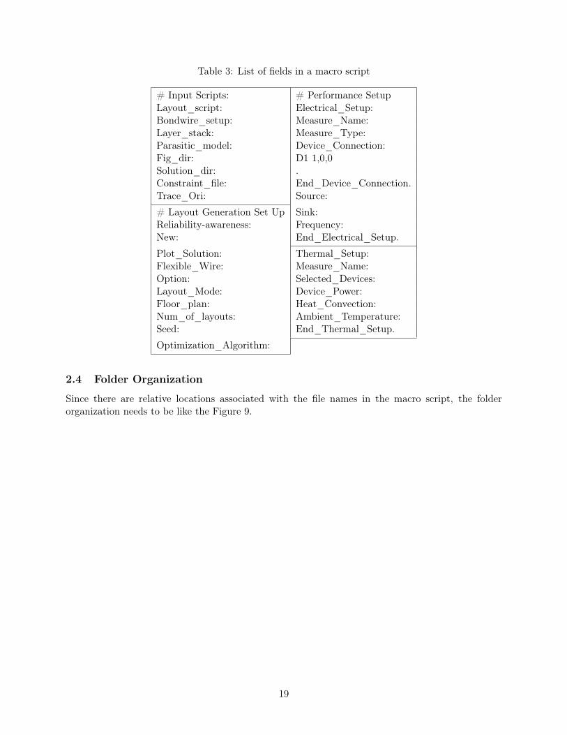
Table 3: List of fields in a macro script
# Input Scripts: # Performance SetupLayout_script: Electrical_Setup:Bondwire_setup: Measure_Name:Layer_stack: Measure_Type:Parasitic_model: Device_Connection:Fig_dir: D1 1,0,0Solution_dir: .Constraint_file: End_Device_Connection.Trace_Ori: Source:
# Layout Generation Set Up Sink:Reliability-awareness: Frequency:New: End_Electrical_Setup.
Plot_Solution: Thermal_Setup:Flexible_Wire: Measure_Name:Option: Selected_Devices:Layout_Mode: Device_Power:Floor_plan: Heat_Convection:Num_of_layouts: Ambient_Temperature:Seed: End_Thermal_Setup.
Optimization_Algorithm:
2.4 Folder Organization
Since there are relative locations associated with the file names in the macro script, the folderorganization needs to be like the Figure 9.
19
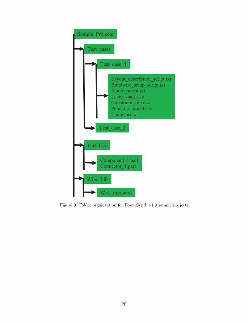
Sample_Projects
Test_cases
Test_case_1
Layout_description_script.txt
Bondwire_setup_script.txt
Macro_script.txt
Layer_stack.csv
Constraint_file.csv
Parasitic_model.csv
Trace_ori.txt
Test_case_2
Part_Lib
Wire_Lib
Component_1.part
Connector_1.part
Wire_info.wire
Figure 9: Folder organization for PowerSynth v1.9 sample projects
20
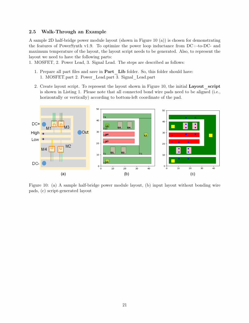
2.5 Walk-Through an Example
A sample 2D half-bridge power module layout (shown in Figure 10 (a)) is chosen for demonstratingthe features of PowerSynth v1.9. To optimize the power loop inductance from DC+-to-DC- andmaximum temperature of the layout, the layout script needs to be generated. Also, to represent thelayout we need to have the following parts:1. MOSFET, 2. Power Lead, 3. Signal Lead. The steps are described as follows:
1. Prepare all part files and save in Part_Lib folder. So, this folder should have:1. MOSFET.part 2. Power_Lead.part 3. Signal_Lead.part
2. Create layout script. To represent the layout shown in Figure 10, the initial Layout_scriptis shown in Listing 1. Please note that all connected bond wire pads need to be aligned (i.e.,horizontally or vertically) according to bottom-left coordinate of the pad.
Figure 10: (a) A sample half-bridge power module layout, (b) input layout without bonding wirepads, (c) script-generated layout
21
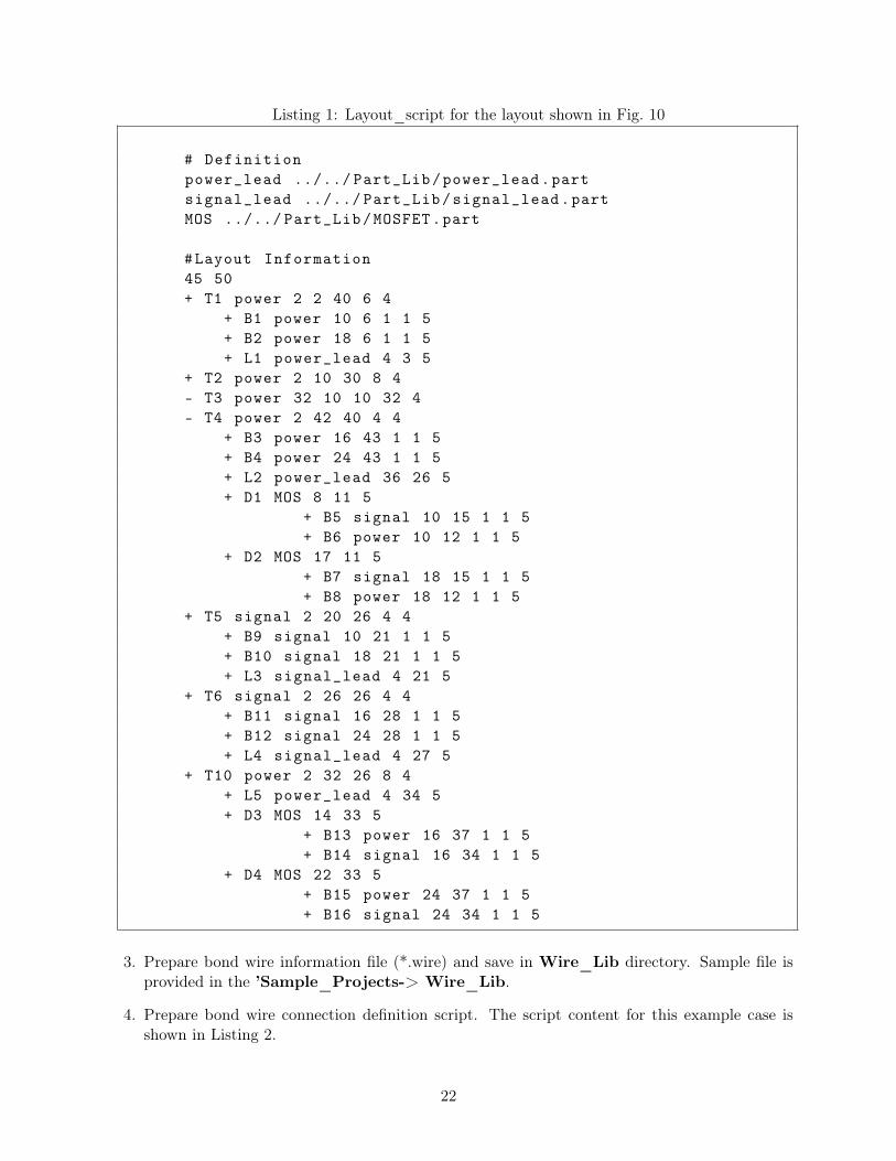
Listing 1: Layout_script for the layout shown in Fig. 10
# Definitionpower_lead ../../ Part_Lib/power_lead.partsignal_lead ../../ Part_Lib/signal_lead.partMOS ../../ Part_Lib/MOSFET.part
#Layout Information45 50+ T1 power 2 2 40 6 4
+ B1 power 10 6 1 1 5+ B2 power 18 6 1 1 5+ L1 power_lead 4 3 5
+ T2 power 2 10 30 8 4- T3 power 32 10 10 32 4- T4 power 2 42 40 4 4
+ B3 power 16 43 1 1 5+ B4 power 24 43 1 1 5+ L2 power_lead 36 26 5+ D1 MOS 8 11 5
+ B5 signal 10 15 1 1 5+ B6 power 10 12 1 1 5
+ D2 MOS 17 11 5+ B7 signal 18 15 1 1 5+ B8 power 18 12 1 1 5
+ T5 signal 2 20 26 4 4+ B9 signal 10 21 1 1 5+ B10 signal 18 21 1 1 5+ L3 signal_lead 4 21 5
+ T6 signal 2 26 26 4 4+ B11 signal 16 28 1 1 5+ B12 signal 24 28 1 1 5+ L4 signal_lead 4 27 5
+ T10 power 2 32 26 8 4+ L5 power_lead 4 34 5+ D3 MOS 14 33 5
+ B13 power 16 37 1 1 5+ B14 signal 16 34 1 1 5
+ D4 MOS 22 33 5+ B15 power 24 37 1 1 5+ B16 signal 24 34 1 1 5
3. Prepare bond wire information file (*.wire) and save in Wire_Lib directory. Sample file isprovided in the ’Sample_Projects-> Wire_Lib.
4. Prepare bond wire connection definition script. The script content for this example case isshown in Listing 2.
22
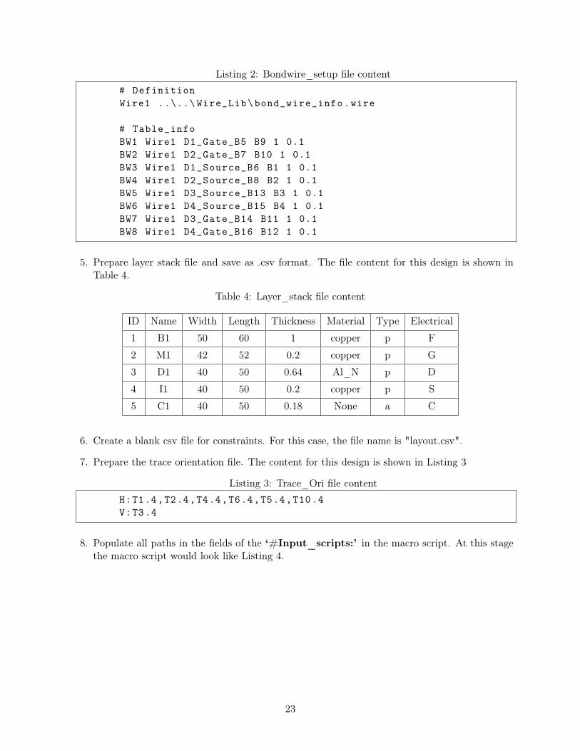
Listing 2: Bondwire_setup file content# DefinitionWire1 ..\..\ Wire_Lib\bond_wire_info.wire
# Table_infoBW1 Wire1 D1_Gate_B5 B9 1 0.1BW2 Wire1 D2_Gate_B7 B10 1 0.1BW3 Wire1 D1_Source_B6 B1 1 0.1BW4 Wire1 D2_Source_B8 B2 1 0.1BW5 Wire1 D3_Source_B13 B3 1 0.1BW6 Wire1 D4_Source_B15 B4 1 0.1BW7 Wire1 D3_Gate_B14 B11 1 0.1BW8 Wire1 D4_Gate_B16 B12 1 0.1
5. Prepare layer stack file and save as .csv format. The file content for this design is shown inTable 4.
Table 4: Layer_stack file content
ID Name Width Length Thickness Material Type Electrical
1 B1 50 60 1 copper p F
2 M1 42 52 0.2 copper p G
3 D1 40 50 0.64 Al_N p D
4 I1 40 50 0.2 copper p S
5 C1 40 50 0.18 None a C
6. Create a blank csv file for constraints. For this case, the file name is "layout.csv".
7. Prepare the trace orientation file. The content for this design is shown in Listing 3
Listing 3: Trace_Ori file contentH:T1.4,T2.4,T4.4,T6.4,T5.4,T10.4V:T3.4
8. Populate all paths in the fields of the ‘#Input_scripts:’ in the macro script. At this stagethe macro script would look like Listing 4.
23
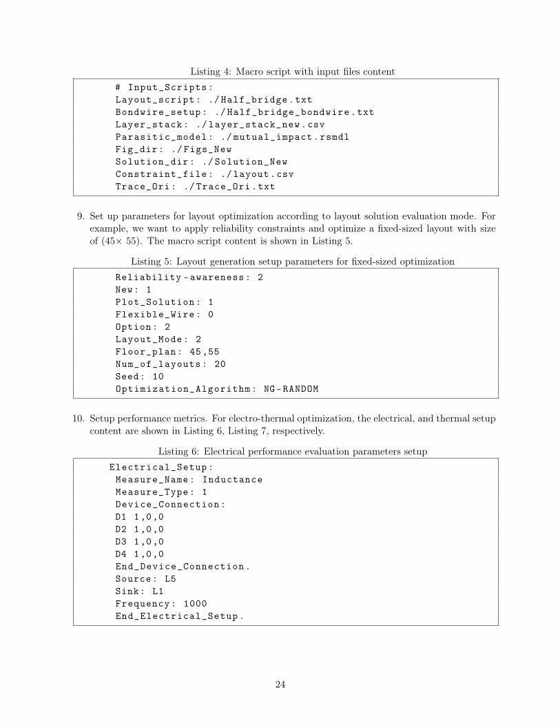
Listing 4: Macro script with input files content# Input_Scripts:Layout_script: ./ Half_bridge.txtBondwire_setup: ./ Half_bridge_bondwire.txtLayer_stack: ./ layer_stack_new.csvParasitic_model: ./ mutual_impact.rsmdlFig_dir: ./ Figs_NewSolution_dir: ./ Solution_NewConstraint_file: ./ layout.csvTrace_Ori: ./ Trace_Ori.txt
9. Set up parameters for layout optimization according to layout solution evaluation mode. Forexample, we want to apply reliability constraints and optimize a fixed-sized layout with sizeof (45× 55). The macro script content is shown in Listing 5.
Listing 5: Layout generation setup parameters for fixed-sized optimizationReliability -awareness: 2New: 1Plot_Solution: 1Flexible_Wire: 0Option: 2Layout_Mode: 2Floor_plan: 45,55Num_of_layouts: 20Seed: 10Optimization_Algorithm: NG-RANDOM
10. Setup performance metrics. For electro-thermal optimization, the electrical, and thermal setupcontent are shown in Listing 6, Listing 7, respectively.
Listing 6: Electrical performance evaluation parameters setupElectrical_Setup:Measure_Name: InductanceMeasure_Type: 1Device_Connection:D1 1,0,0D2 1,0,0D3 1,0,0D4 1,0,0End_Device_Connection.Source: L5Sink: L1Frequency: 1000End_Electrical_Setup.
24
Listing 7: Thermal performance evaluation parameters setupThermal_Setup:# Model : 0 for TSFM or 1 for AnalyticalModel_Select: 0Measure_Name: Max_TemperatureSelected_Devices: D1,D2,D3 ,D4Device_Power: 10,10,10,10Heat_Convection: 100Ambient_Temperature: 300End_Thermal_Setup.
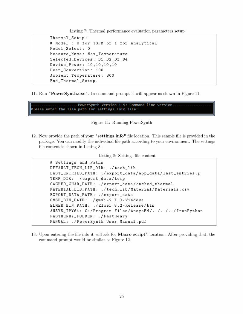
11. Run "PowerSynth.exe". In command prompt it will appear as shown in Figure 11.
Figure 11: Running PowerSynth
12. Now provide the path of your "settings.info" file location. This sample file is provided in thepackage. You can modify the individual file path according to your environment. The settingsfile content is shown in Listing 8.
Listing 8: Settings file content# Settings and PathsDEFAULT_TECH_LIB_DIR: ./ tech_libLAST_ENTRIES_PATH: ./ export_data/app_data/last_entries.pTEMP_DIR: ./ export_data/tempCACHED_CHAR_PATH: ./ export_data/cached_thermalMATERIAL_LIB_PATH: ./ tech_lib/Material/Materials.csvEXPORT_DATA_PATH: ./ export_dataGMSH_BIN_PATH: ./gmsh -2.7.0 - WindowsELMER_BIN_PATH: ./ Elmer_8.2-Release/binANSYS_IPY64: C:/ Program Files/AnsysEM /../../../ IronPythonFASTHENRY_FOLDER: ./ FastHenryMANUAL: ./ PowerSynth_User_Manual.pdf
13. Upon entering the file info it will ask for Macro script" location. After providing that, thecommand prompt would be similar as Figure 12.
25
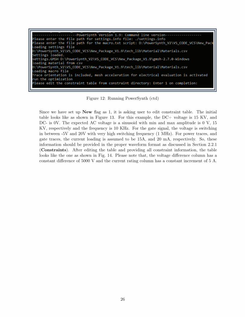
Figure 12: Running PowerSynth (ctd)
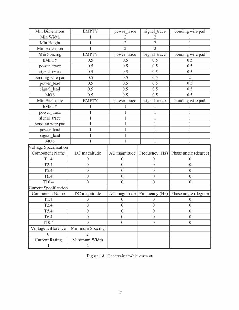
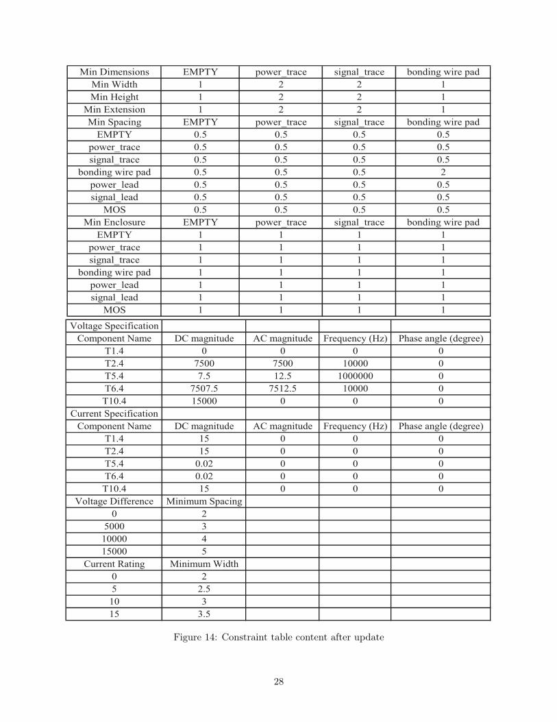
Since we have set up New flag as 1, it is asking user to edit constraint table. The initialtable looks like as shown in Figure 13. For this example, the DC+ voltage is 15 KV, andDC- is 0V. The expected AC voltage is a sinusoid with min and max amplitude is 0 V, 15KV, respectively and the frequency is 10 KHz. For the gate signal, the voltage is switchingin between -5V and 20V with very high switching frequency (1 MHz). For power traces, andgate traces, the current loading is assumed to be 15A, and 20 mA, respectively. So, theseinformation should be provided in the proper waveform format as discussed in Section 2.2.1(Constraints). After editing the table and providing all constraint information, the tablelooks like the one as shown in Fig. 14. Please note that, the voltage difference column has aconstant difference of 5000 V and the current rating column has a constant increment of 5 A.
26
Min Dimensions EMPTY power_trace signal_trace bonding wire pad
Min Width 1 2 2 1
Min Height 1 2 2 1
Min Extension 1 2 2 1
Min Spacing EMPTY power_trace signal_trace bonding wire pad
EMPTY 0.5 0.5 0.5 0.5
power_trace 0.5 0.5 0.5 0.5
signal_trace 0.5 0.5 0.5 0.5
bonding wire pad 0.5 0.5 0.5 2
power_lead 0.5 0.5 0.5 0.5
signal_lead 0.5 0.5 0.5 0.5
MOS 0.5 0.5 0.5 0.5
Min Enclosure EMPTY power_trace signal_trace bonding wire pad
EMPTY 1 1 1 1
power_trace 1 1 1 1
signal_trace 1 1 1 1
bonding wire pad 1 1 1 1
power_lead 1 1 1 1
signal_lead 1 1 1 1
MOS 1 1 1 1
Voltage Specification
Component Name DC magnitude AC magnitude Frequency (Hz) Phase angle (degree)
T1.4 0 0 0 0
T2.4 0 0 0 0
T5.4 0 0 0 0
T6.4 0 0 0 0
T10.4 0 0 0 0
Current Specification
Component Name DC magnitude AC magnitude Frequency (Hz) Phase angle (degree)
T1.4 0 0 0 0
T2.4 0 0 0 0
T5.4 0 0 0 0
T6.4 0 0 0 0
T10.4 0 0 0 0
Voltage Difference Minimum Spacing
0 2
Current Rating Minimum Width
1 2
Figure 13: Constraint table content
27
Min Dimensions EMPTY power_trace signal_trace bonding wire pad
Min Width 1 2 2 1
Min Height 1 2 2 1
Min Extension 1 2 2 1
Min Spacing EMPTY power_trace signal_trace bonding wire pad
EMPTY 0.5 0.5 0.5 0.5
power_trace 0.5 0.5 0.5 0.5
signal_trace 0.5 0.5 0.5 0.5
bonding wire pad 0.5 0.5 0.5 2
power_lead 0.5 0.5 0.5 0.5
signal_lead 0.5 0.5 0.5 0.5
MOS 0.5 0.5 0.5 0.5
Min Enclosure EMPTY power_trace signal_trace bonding wire pad
EMPTY 1 1 1 1
power_trace 1 1 1 1
signal_trace 1 1 1 1
bonding wire pad 1 1 1 1
power_lead 1 1 1 1
signal_lead 1 1 1 1
MOS 1 1 1 1
Voltage Specification
Component Name DC magnitude AC magnitude Frequency (Hz) Phase angle (degree)
T1.4 0 0 0 0
T2.4 7500 7500 10000 0
T5.4 7.5 12.5 1000000 0
T6.4 7507.5 7512.5 10000 0
T10.4 15000 0 0 0
Current Specification
Component Name DC magnitude AC magnitude Frequency (Hz) Phase angle (degree)
T1.4 15 0 0 0
T2.4 15 0 0 0
T5.4 0.02 0 0 0
T6.4 0.02 0 0 0
T10.4 15 0 0 0
Voltage Difference Minimum Spacing
0 2
5000 3
10000 4
15000 5
Current Rating Minimum Width
0 2
5 2.5
10 3
15 3.5
Figure 14: Constraint table content after update
28
Once editing the constraint table, enter 1 in the command line. Then it will generate 20solutions and several files will be saved in “Solution_dir” and “Fig_dir”. Results can be foundin "Sample_Projects/Test_Cases/Half_Bridge_2" folder in the package.
For large number of solutions, we should turn off “Plot_Solutions” flag, otherwise you mayencounter “memory” issue in python. To use the updated constraint table, user should turnoff the “New” flag, otherwise each time user runs PowerSynth.exe with the same macro script,it asks for editing constraint table and overwrite the modified values with the default values.By changing “Option”, “Layout_Mode”, user can use PowerSynth according to the necessity.
3 PowerSynth-Related Publications
This section contains a list of all the current publications related to PowerSynth as of the date ofthis document.
1. P. Tucker, "SPICE netlist generation for electrical parasitic modeling of multi-chip powermodule designs," 2013.
2. B. W. Shook, A. Nizam, Z. Gong, A. M. Francis and H. A. Mantooth, "Multi-objective lay-out optimization for multi-chip power modules considering electrical parasitics and thermalperformance," in Control and Modeling for Power Electronics (COMPEL), 2013 IEEE 14thWorkshop on, 2013.
3. B. W. Shook, Z. Gong, Y. Feng, A. M. Francis and H. A. Mantooth, "Multi-chip power modulefast thermal modeling for layout optimization," Computer-Aided Design and Applications, vol.9, pp. 837-846, 2012.
4. B. W. Shook, "The Design and Implementation of a Multi-Chip Power Module Layout Syn-thesis Tool," 2014.
5. J. Main, "A Manufacturer Design Kit for Multi-Chip Power Module Layout Synthesis," 2017.
6. Q. Le, T. Evans, S. Mukherjee, Y. Peng, T. Vrotsos and H. A. Mantooth, "Response surfacemodeling for parasitic extraction for multi-objective optimization of multi-chip power modules(MCPMs)," in Wide Bandgap Power Devices and Applications (WiPDA), 2017 IEEE 5thWorkshop on, 2017.
7. Q. Le, S. Mukherjee, T. Vrotsos and H. A. Mantooth, "Fast transient thermal and powerdissipation modeling for multi-chip power modules: A preliminary assessment of differentelectro-thermal evaluation methods," in Control and Modeling for Power Electronics (COM-PEL), 2016 IEEE 17th Workshop on, 2016.
8. Z. Gong, "Thermal and electrical parasitic modeling for multi-chip power module layout syn-thesis," 2012.
9. S. Mukherjee et al, "Toward Partial Discharge Reduction by Corner Correction in PowerModule Layouts," in Control and Modeling for Power Electronics (COMPEL), pp. 1–8, Jun2018.
10. I. Al Razi et al, "Constraint-Aware Algorithms for Heterogeneous Power Module LayoutSynthesis and Reliability Optimization," in Wide Bandgap Power Devices and Applications(WiPDA), pp. 323–330, Oct 2018.
29
11. T. Evans, Q. Le, S. Mukherjee, I. Al Razi, T. Vrotsos, Y. Peng and H. A. Mantooth, "Power-Synth: A Module Layout Generation Tool," in IEEE Transactions on Power Electronics, vol.34, no. 6, pp. 5063–5078, Jun 2019, Highlighted Paper.
12. Q. Le et al, "PEEC Method and Hierarchical Approach Towards 3D Multichip Power Module(MCPM) Layout Optimization", in Proc. IEEE International Workshop on Integrated PowerPackaging, pp. 131–136, Apr 2019.
13. I. Al Razi et al, "Hierarchical Layout Synthesis and Design Automation for 2.5D HeterogeneousMulti-Chip Power Modules", in Proc. IEEE Energy Conversion Congress and Exposition, pp.2257-2263, Sep 2019.
14. T. Evans et al, "Development of EDA Techniques for Power Module EMI Modeling and LayoutOptimization", in Proc. IMAPS International Symposium on Microelectronics, pp. 193-198,Oct 2019.
15. Y. Peng et al, "PowerSynth Progression on Layout Optimization for Reliability and SignalIntegrity", IEICE Nonlinear Theory and Its Applications, vol. 11, no. 2, pp. 124-144, Apr2020, Invited Paper.
16. I. Al Razi et al, "Physical Design Automation for High-Density 3D Power Module LayoutSynthesis and Optimization", (accepted) in Proc. IEEE Energy Conversion Congress andExposition, 2020.
17. T. Evans et al, "Electronic Design Automation Tools and Considerations for Electro-Thermo-Mechanical Co-Design of High Voltage Power Modules", (accepted) in Proc. IEEE EnergyConversion Congress and Exposition, 2020.
18. S. Mukherjee et al, "General Equation to Determine Design Rules for Mitigating Partial Dis-charge and Electrical Breakdown in Power Module Layouts", (accepted) in Proc. IEEE Work-shop on Wide Bandgap Power Devices and Applications in Asia, 2020.
3.1 Useful Links
• Release Website: https://e3da.csce.uark.edu/release/PowerSynth/
• Publication Website: https://e3da.csce.uark.edu/pub/
30

4 Authors
The PowerSynth tool development is on-going for a decade now and the current PowerSynth teamappreciates efforts from quite a few number of graduate students and numerous undergraduatestudents over the years.
4.1 Graduate Research Assistants
The PowerSynth research and development team worked on this version (v1.9) consists of four Ph.D.students from different disciplines, who are supervised by two professors. A brief introduction tothe authors are as follows:
• Imam Al RaziPh.D. StudentComputer Science and Computer Engineering DepartmentUniversity of Arkansas, Fayetteville, AR, USA.
• Quang LePh.D. StudentElectrical Engineering DepartmentUniversity of Arkansas, Fayetteville, AR, USA.
• Tristan M. EvansPh.D. StudentElectrical Engineering DepartmentUniversity of Arkansas, Fayetteville, AR, USA.
• Shilpi MukherjeePh.D. StudentMicroelectronics and Photonics DepartmentUniversity of Arkansas, Fayetteville, AR, USA.
4.2 Supervisors
• Dr. Homer Alan MantoothDistinguished Professor, The Twenty-First Century Research Leadership Chair in EngineeringDepartment of Electrical Engineering, University of Arkansas, Fayetteville, AR, USA.Phone: 479-575-4838Email: [email protected]
• Dr. Yarui PengAssistant ProfessorComputer Science and Computer Engineering DepartmentUniversity of Arkansas, Fayetteville, AR, USA.Phone: 479-575-6043Email: [email protected]
31