Embed Size (px)
Citation preview
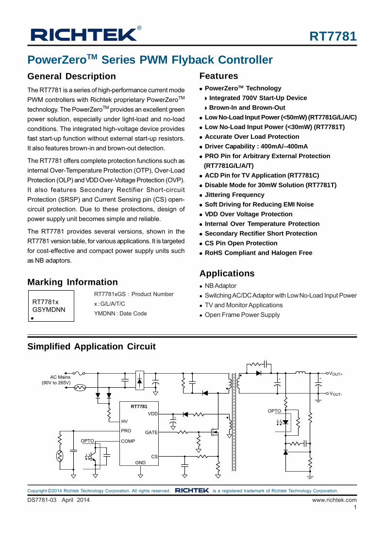
RT7781®
DS7781-03 April 2014 www.richtek.com1
Copyright 2014 Richtek Technology Corporation. All rights reserved. is a registered trademark of Richtek Technology Corporation.©
General Description
The RT7781 is a series of high-performance current mode
PWM controllers with Richtek proprietary PowerZeroTM
technology. The PowerZeroTM provides an excellent green
power solution, especially under light-load and no-load
conditions. The integrated high-voltage device provides
fast start-up function without external start-up resistors.
It also features brown-in and brown-out detection.
The RT7781 offers complete protection functions such as
internal Over-Temperature Protection (OTP), Over-Load
Protection (OLP) and VDD Over-Voltage Protection (OVP).
It also features Secondary Rectifier Short-circuit
Protection (SRSP) and Current Sensing pin (CS) open-
circuit protection. Due to these protections, design of
power supply unit becomes simple and reliable.
The RT7781 provides several versions, shown in the
RT7781 version table, for various applications. It is targeted
for cost-effective and compact power supply units such
as NB adaptors.
PowerZeroTM Series PWM Flyback ControllerFeatures PowerZeroTM Technology
Integrated 700V Start-Up Device
Brown-In and Brown-Out
Low No-Load Input Power (<50mW) (RT7781G/L/A/C)
Low No-Load Input Power (<30mW) (RT7781T)
Accurate Over Load Protection
Driver Capability : 400mA/−−−−−400mA
PRO Pin for Arbitrary External Protection
(RT7781G/L/A/T)
ACD Pin for TV Application (RT7781C)
Disable Mode for 30mW Solution (RT7781T)
Jittering Frequency
Soft Driving for Reducing EMI Noise
VDD Over Voltage Protection
Internal Over Temperature Protection
Secondary Rectifier Short Protection
CS Pin Open Protection
RoHS Compliant and Halogen Free
Simplified Application Circuit
Applications NB Adaptor
Switching AC/DC Adaptor with Low No-Load Input Power
TV and Monitor Applications
Open Frame Power Supply
VOUT+
PRO
COMP
GND
VDD
GATE
CS
RT7781
AC Mains(90V to 265V)
VOUT-
HV
OPTO
OPTO
+
++
Marking InformationRT7781xGS : Product Number
x : G/L/A/T/C
YMDNN : Date Code
RT7781xGSYMDNN

RT7781
2 DS7781-03 April 2014
©Copyright 2014 Richtek Technology Corporation. All rights reserved. is a registered trademark of Richtek Technology Corporation.
Version RT7781G RT7781L RT7781A RT7781T RT7781C
Frequency 65kHz 65kHz 65kHz 65kHz 65kHz
OLP and SRSP Auto Recovery Auto Recovery Latch Auto Recovery Auto Recovery
OLP Delay Time 56ms 56ms 56ms 56ms 56ms
VDD OVP (27V) Auto Recovery Latch Latch Latch Auto Recovery
VPRO > 1.8V Latch Latch Latch Latch X
0.5V > VPRO > 0.3V Auto Recovery Latch Latch Latch X
VPRO < 0.3V Auto Recovery Auto Recovery Latch Auto Recovery X
ACD Pin X X X X Yes
Disable Mode X X X Yes X
RT7781 Version Table
Ordering Information
Note :
Richtek products are :
RoHS compliant and compatible with the current require-
ments of IPC/JEDEC J-STD-020.
Suitable for use in SnPb or Pb-free soldering processes.
RT7781
Package TypeS : SOP-7
Lead Plating SystemG : Green (Halogen Free and Pb Free)
RT7781 Version (Refer to Version Table)
Pin Configurations
(TOP VIEW)
ACD
COMP
CS
GND
HV
GATE
VDD
2
3
4 5
6
7
PRO
COMP
CS
GND
HV
GATE
VDD
2
3
4 5
6
7
RT7781G/L/A/T
SOP-7
RT7781C
SOP-7

RT7781
3DS7781-03 April 2014
©Copyright 2014 Richtek Technology Corporation. All rights reserved. is a registered trademark of Richtek Technology Corporation.
Functional Pin Description
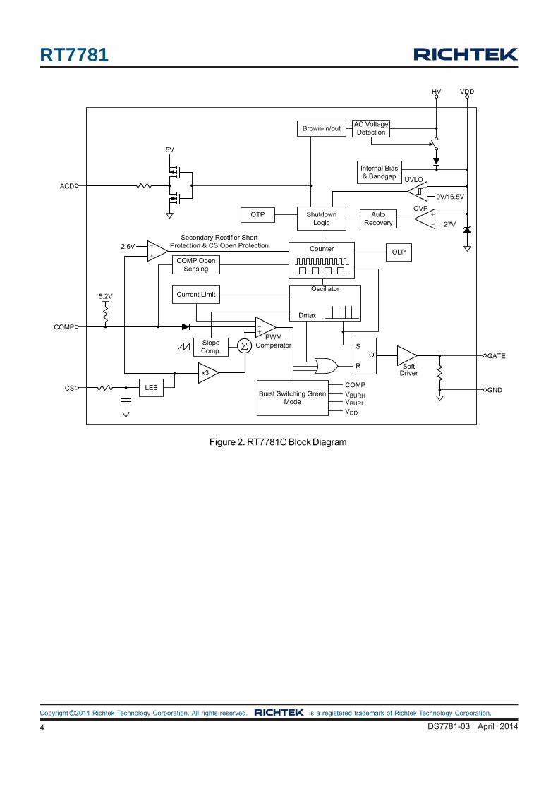
Function Block Diagram
Figure 1. RT7781G/L/A/T Block Diagram
Pin No. Pin Name Pin Description
PRO External Protection Input for OVP or OTP. (RT7781G/L/A/T) 1
ACD Output for AC Voltage Brown-Out Detection. (RT7781C)
2 COMP Feedback Voltage Input. Connect an opto-coupler to close the control loop and achieve output voltage regulation.
3 CS Current Sense Input. The current sense resistor between this pin and GND is used for current limit setting.
4 GND Ground of the Controller.
5 GATE Gate Driver Output for the External MOSFET.
6 VDD Supply Voltage Input. The controller will be enabled when VDD exceeds VTH_ON and disabled when VDD decreases lower than VTH_OFF.
7 HV High Voltage Input for Start-Up. This pin can withstand high voltage up to 700V.
VDD
27V
HV
9V/16.5V
Internal Bias& Bandgap
Shutdown Logic
Burst Switching Green Mode
Slope Comp.
LEB
Oscillator
Dmax
Counter
OTP
Auto Recovery
GATE
COMP
CS
PRO
56ms Debounce
Deglitch
OLP
OVP
VTH_H
Deglitch
IBIAS
Latch
2VSecondary Rectifier Short
Protection & CS Open Protection
+
-
+
-
+
-
+
-
+-
x3R
SQ
+
-
+
-
GND
VTH_OTP
VTH_L
COMP Open Sensing
-
PWM Comparator
UVLO
AC Voltage Detection
Brown-in/out
Current Limit
Soft Driver
Latch
Auto Recovery
Latch
Disable Mode (T Version Only)
Auto Recovery
Latch
5.2V
COMP
VDD
VBURL
VBURH
RT7781
4 DS7781-03 April 2014
©Copyright 2014 Richtek Technology Corporation. All rights reserved. is a registered trademark of Richtek Technology Corporation.
Figure 2. RT7781C Block Diagram
VDD
27V
HV
9V/16.5V
Internal Bias& Bandgap
Shutdown Logic
Slope Comp.
LEB
Oscillator
Dmax
Counter
OTP Auto Recovery
GATE
COMP
CS
ACD
OLP
OVP
2.6VSecondary Rectifier Short
Protection & CS Open Protection
+
-
+-
x3R
SQ
+
-
+
-
GND
COMP Open Sensing
-
PWM Comparator
UVLO
Current Limit
Soft Driver
5V
5.2V
AC Voltage Detection
Brown-in/out
Burst Switching Green Mode
COMP
VDD
VBURL
VBURH

RT7781
5DS7781-03 April 2014
©Copyright 2014 Richtek Technology Corporation. All rights reserved. is a registered trademark of Richtek Technology Corporation.
Oscillator
The oscillator runs at 65kHz and features frequency
jittering function. Its jittering depth is 6% with about 4ms
envelope frequency at 65kHz. It also generates slope
compensation saw-tooth, 75% maximum duty cycle pulse
and over-load protection slope.
Leading Edge Blanking (LEB)
Due to the device parasitic capacitors, an initial current
spike appears on the current sense resistor at the
beginning of the power MOSFET on-state. The spike of
the CS voltage may incorrectly trigger the peak current
comparator to turn off the power MOSFET, resulting in
running failure of the Flyback converter. Thus, the LEB
time used to mask the initial voltage spike on the CS pin,
is a necessary design for a successful PWM operation.
Gate Driver
A totem pole gate driver is designed to meet both of low
EMI and high efficiency application requirements. The driver
integrates a voltage clamping circuit to limit the max.
GATE output voltage at high VDD supply voltage
condition(VDD > 15V). An internal pull low circuit is
activated to prevent the external MOSFET from accidental
turning-on when the VDD is pretty low during a start-up
process.
Cycle-by-Cycle Current Limit & Constant Power
This is a basic but very useful function and it can be
implemented easily in current mode controller. The entry
points of current limit are different for low line and high
line AC inputs because of the effect from different peak
currents with the same propagation delay time. The
RT7781 provides a unique calibration mechanism to
reduce the variation and achieves constant output power
between 90Vac and 265Vac.
COMP Pin Open Protection
If the COMP voltage reaches the open voltage VCOMP_OP,
the controller will shut down after about tOLP and enter
auto recovery mode.
Operation
HV pin Detection
The RT7781 provides a 700V high voltage pin to detect
the AC input voltage and supports startup.
Brown-In and Brown-Out
The brown-in and brown-out functions are designed in this
controller. Therefore, the components and power loss of
external brown-in and brown-out circuits can be eliminated.
When the HV voltage rises above the brown-in voltage
threshold (VTH_BI = 113V typ.) for more than the brown-in
deglitch time, the IC enters brown-in condition and starts
PWM switching. When the HV voltage keeps under the
brown-out voltage threshold (VTH_BO = 96V typ.) for more
than the brown-out debounce time (tD_BO), the IC enters
brown-out condition and stops PWM switching.
Burst Switching Green Mode
The burst mode is designed to reduce switching loss at
light load condition. When the output load gets light, the
COMP voltage drops and reaches VBURL, the controller
will cease switching. After the output voltage drops and
the COMP voltage goes up to VBURH, the controller will
resume switching.
VDD Holdup Mode
The RT7781 provides a unique operation mode at almost
no load condition named VDD holdup mode. Under the
VDD holdup mode, the RT7781 forces PWM switching to
maintain VDD voltage between VDD_ET and VDD_ED. The
benefit of the VDD holdup mode is to avoid the VDD drops
to VTH_OFF due to the long burst mode period at no load or
load transient moment. Therefore, this function makes bias
winging design and transient design easier and compacter.
Disable Mode (T Version Only)
The RT7781T, designed to cooperate with the specific
secondary-side voltage regulator RT7205, provides an
outstanding solution with ultra low no-load input power
(<30mW). The RT7781T features the disable mode to
minimize the power consumption at very light-load or no-
load conditions.
RT7781
6 DS7781-03 April 2014
©Copyright 2014 Richtek Technology Corporation. All rights reserved. is a registered trademark of Richtek Technology Corporation.
Accurate Over-Load Protection Over AC Input
Voltage Range
In normal operation, the CS peak voltage is controlled by
the COMP voltage. In output over-load conditions, the CS
peak voltage must be limited (regardless of the COMP
voltage) to protect the load device and converter. This
operation is called cycle-by-cycle current limit. When the
duration of the current-limit operation reaches the Over-
Load Protection (OLP) debounce time, the OLP shuts
down the converter.
In over load conditions, long time operation of the cycle-
by-cycle current limit will lead to system thermal stress
problem. To further protect the system, the RT7781 is
designed with a proprietary function to prolong the turn-
off period during hiccup operation. Thus, the average power
loss and the temperature of each component in the
converter will be reduced to an acceptable level during
long-time output over-load conditions.
In general, the OLP trip level is a function of the AC input
voltage. For improving the accuracy of the OLP level over
the full range of AC input voltage, the RT7781 is equipped
with an OLP level compensation function. This function is
that the maximum CS voltage threshold in the cycle-by-
cycle current limit operation is modulated by the GATE
on-time. It means that smaller GATE on-time gets smaller
maximum CS voltage threshold. Therefore, the total
variation of the OLP trip level over the full range of AC
input voltage is minimized.
Over Voltage Protection
Output voltage can be roughly sensed by VDD pin. If the
sensed voltage reaches VOVP threshold, the controller will
shut down after the OVP deglitch time.
CS Pin Open Protection
When CS pin is opened, the controller will shut down
after a couple of cycles and enter auto recovery mode.
Secondary Rectifier Short Protection (SRSP)
The RT7781 is equipped with the SRSP against the
secondary rectifier short-circuit condition in a flyback
converter. As the output rectifier is damaged as short-
circuit and the power MOSFET is turned on, inrush
currents which flow through the power MOSFET, primary
and secondary windings are very huge and may cause
magnetic saturation of the transformer. Due the huge
current stress, the power components can not sustain
the stress until the end of the OLP debounce time. The
SRSP function is a necessary design for protecting the
power components. When CS voltage reaches the SRSP
voltage threshold, the RT7781 shuts down the converter
after the debounce time of few switching cycles.

RT7781
7DS7781-03 April 2014
©Copyright 2014 Richtek Technology Corporation. All rights reserved. is a registered trademark of Richtek Technology Corporation.
Electrical Characteristics
Recommended Operating Conditions (Note 4)
Supply Input Voltage, HV ------------------------------------------------------------------------------------------- 0V to 500V (DC)
Supply Input Voltage, VDD ----------------------------------------------------------------------------------------- 12V to 25V
Junction Temperature Range--------------------------------------------------------------------------------------- −40°C to 125°C Ambient Temperature Range--------------------------------------------------------------------------------------- −40°C to 85°C
Absolute Maximum Ratings (Note 1)
HV to GND ------------------------------------------------------------------------------------------------------------- −0.3V to 700V (DC)
Supply Input Voltage, VDD to GND ------------------------------------------------------------------------------- −0.3V to 30V
GATE to GND --------------------------------------------------------------------------------------------------------- −0.3V to 16.5V
PRO, COMP, CS to GND ------------------------------------------------------------------------------------------- −0.3V to 6.5V
Power Dissipation, PD @ TA = 25°C SOP-7 ------------------------------------------------------------------------------------------------------------------- 0.36W
Package Thermal Resistance (Note 2)
SOP-7, θJA ------------------------------------------------------------------------------------------------------------- 276.5°C/W
Junction Temperature ------------------------------------------------------------------------------------------------ 150°C Lead Temperature (Soldering, 10 sec.) -------------------------------------------------------------------------- 260°C Storage Temperature Range --------------------------------------------------------------------------------------- −65°C to 150°C ESD Susceptibility (Note 3)
HBM (Human Body Model)
(Except HV pin) ------------------------------------------------------------------------------------------------------- 5kV
(HV to GND) ----------------------------------------------------------------------------------------------------------- 1kV
MM (Machine Model) ------------------------------------------------------------------------------------------------ 300V
(VDD = 15V, TA = 25°C, unless otherwise specified)
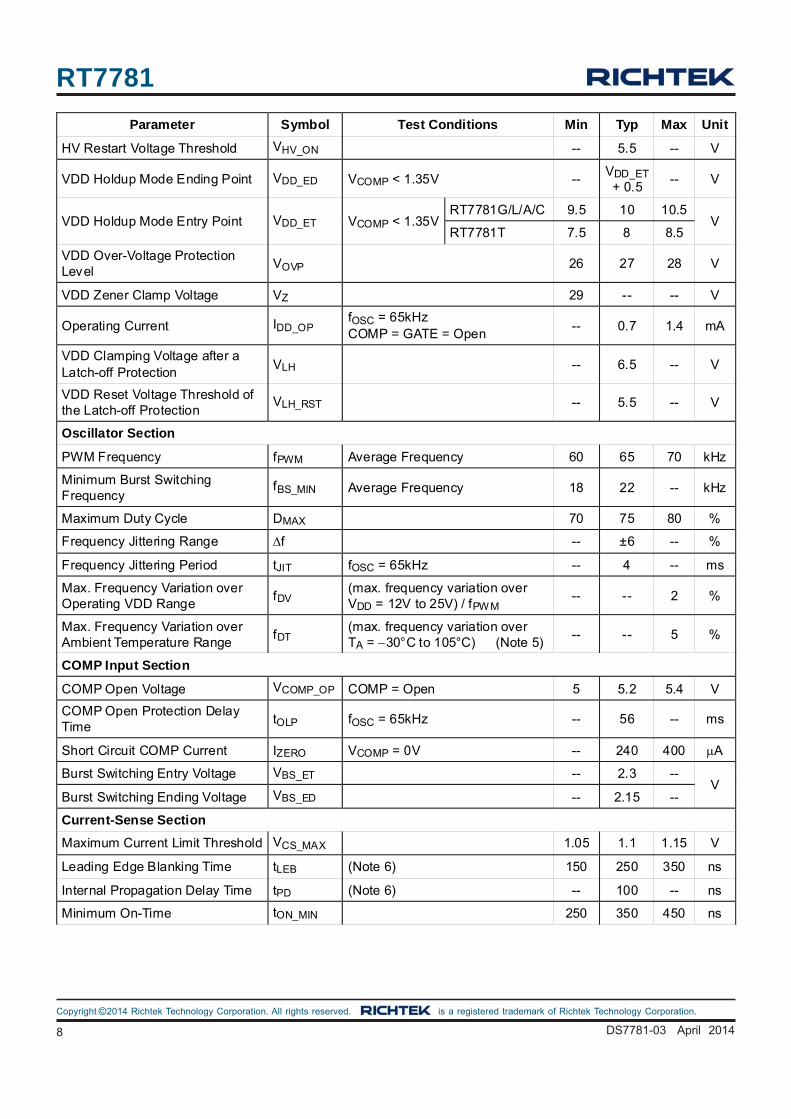
Parameter Symbol Test Conditions Min Typ Max Unit
HV Section
HV Start-Up Current IJEFT_ST VDD < VTH_ON, VHV = 500V 1 3.5 -- mA
Off State Leakage Current IHV_LK VDD > VTH_ON, VHV = 500V -- -- 25 A
Brown-In Threshold VTH_BI DC Input Voltage 106 113 120 V
Brown-Out Threshold VTH_BO DC Input Voltage 86 96 106 V
Brown-In/Out Hysteresis VBIO VBIO = VTH_BI VTH_BO 10 17 27 V
De-Bounce Time of Brown-Out tD_BO fOSC = 65kHz -- 60 --
ms fOSC = 22kHz -- 180 --
VDD Section
Under Voltage Lockout (UVLO) Voltage Threshold (On)
VTH_ON 15.5 16.5 17.5 V
Under Voltage Lockout (UVLO) Voltage Threshold (Off)
VTH_OFF RT7781G/L/A/C 8.5 9 9.5
V RT7781T 6.5 7 7.5
RT7781
8 DS7781-03 April 2014
©Copyright 2014 Richtek Technology Corporation. All rights reserved. is a registered trademark of Richtek Technology Corporation.
Parameter Symbol Test Conditions Min Typ Max Unit
HV Restart Voltage Threshold VHV_ON -- 5.5 -- V
VDD Holdup Mode Ending Point VDD_ED VCOMP < 1.35V -- VDD_ET + 0.5
-- V
VDD Holdup Mode Entry Point VDD_ET VCOMP < 1.35V RT7781G/L/A/C 9.5 10 10.5
V RT7781T 7.5 8 8.5
VDD Over-Voltage Protection Level
VOVP 26 27 28 V
VDD Zener Clamp Voltage VZ 29 -- -- V
Operating Current IDD_OP fOSC = 65kHz COMP = GATE = Open
-- 0.7 1.4 mA
VDD Clamping Voltage after a Latch-off Protection
VLH -- 6.5 -- V
VDD Reset Voltage Threshold of the Latch-off Protection
VLH_RST -- 5.5 -- V
Oscillator Section
PWM Frequency fPWM Average Frequency 60 65 70 kHz
Minimum Burst Switching Frequency
fBS_MIN Average Frequency 18 22 -- kHz
Maximum Duty Cycle DMAX 70 75 80 %
Frequency Jittering Range f -- ±6 -- %
Frequency Jittering Period tJIT fOSC = 65kHz -- 4 -- ms
Max. Frequency Variation over Operating VDD Range
fDV (max. frequency variation over VDD = 12V to 25V) / fPW M
-- -- 2 %
Max. Frequency Variation over Ambient Temperature Range
fDT (max. frequency variation over TA = 30°C to 105°C) (Note 5)
-- -- 5 %
COMP Input Section
COMP Open Voltage VCOMP_OP COMP = Open 5 5.2 5.4 V
COMP Open Protection Delay Time
tOLP fOSC = 65kHz -- 56 -- ms
Short Circuit COMP Current IZERO VCOMP = 0V -- 240 400 A
Burst Switching Entry Voltage VBS_ET -- 2.3 -- V
Burst Switching Ending Voltage VBS_ED -- 2.15 --
Current-Sense Section
Maximum Current Limit Threshold VCS_MAX 1.05 1.1 1.15 V
Leading Edge Blanking Time tLEB (Note 6) 150 250 350 ns
Internal Propagation Delay Time tPD (Note 6) -- 100 -- ns
Minimum On-Time tON_MIN 250 350 450 ns
RT7781
9DS7781-03 April 2014
©Copyright 2014 Richtek Technology Corporation. All rights reserved. is a registered trademark of Richtek Technology Corporation.
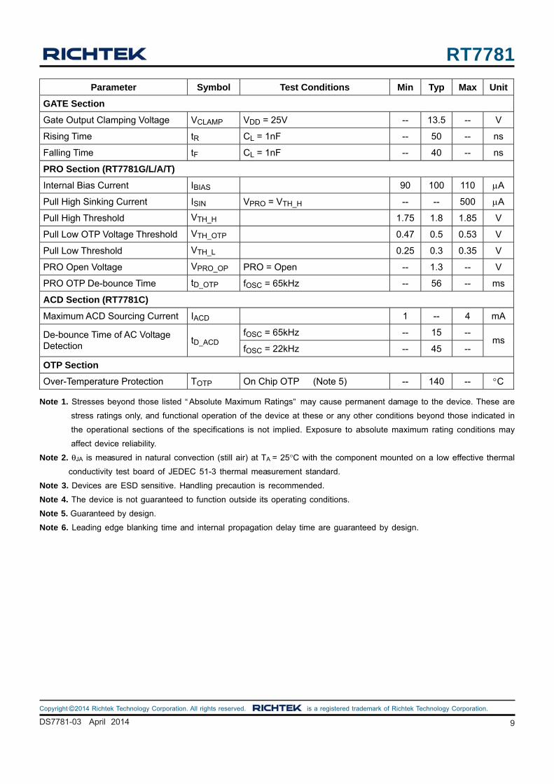
Note 1. Stresses beyond those listed “Absolute Maximum Ratings” may cause permanent damage to the device. These are
stress ratings only, and functional operation of the device at these or any other conditions beyond those indicated in
the operational sections of the specifications is not implied. Exposure to absolute maximum rating conditions may
affect device reliability.
Note 2. θJA is measured in natural convection (still air) at TA = 25°C with the component mounted on a low effective thermal
conductivity test board of JEDEC 51-3 thermal measurement standard.
Note 3. Devices are ESD sensitive. Handling precaution is recommended.
Note 4. The device is not guaranteed to function outside its operating conditions.
Note 5. Guaranteed by design.
Note 6. Leading edge blanking time and internal propagation delay time are guaranteed by design.
Parameter Symbol Test Conditions Min Typ Max Unit
GATE Section
Gate Output Clamping Voltage VCLAMP VDD = 25V -- 13.5 -- V
Rising Time tR CL = 1nF -- 50 -- ns
Falling Time tF CL = 1nF -- 40 -- ns
PRO Section (RT7781G/L/A/T)
Internal Bias Current IBIAS 90 100 110 A
Pull High Sinking Current ISIN VPRO = VTH_H -- -- 500 A
Pull High Threshold VTH_H 1.75 1.8 1.85 V
Pull Low OTP Voltage Threshold VTH_OTP 0.47 0.5 0.53 V
Pull Low Threshold VTH_L 0.25 0.3 0.35 V
PRO Open Voltage VPRO_OP PRO = Open -- 1.3 -- V
PRO OTP De-bounce Time tD_OTP fOSC = 65kHz -- 56 -- ms
ACD Section (RT7781C)
Maximum ACD Sourcing Current IACD 1 -- 4 mA
fOSC = 65kHz -- 15 -- De-bounce Time of AC Voltage Detection
tD_ACD fOSC = 22kHz -- 45 --
ms
OTP Section
Over-Temperature Protection TOTP On Chip OTP (Note 5) -- 140 -- C
RT7781
10 DS7781-03 April 2014
©Copyright 2014 Richtek Technology Corporation. All rights reserved. is a registered trademark of Richtek Technology Corporation.
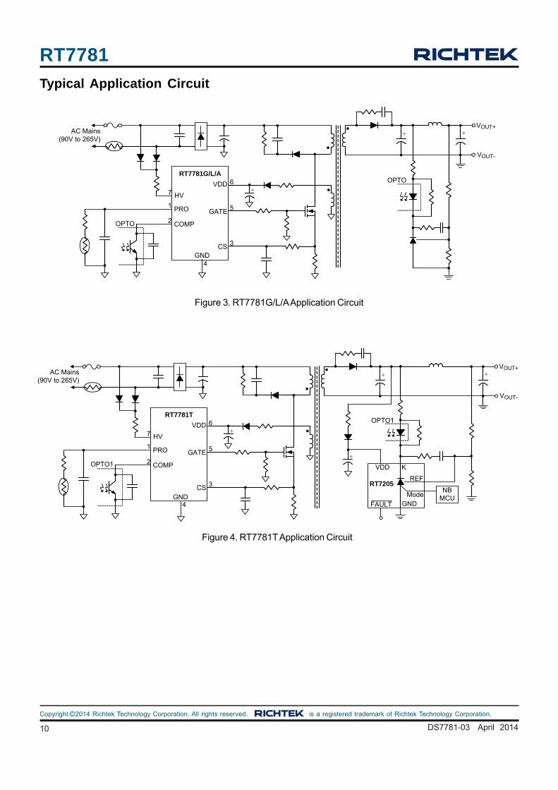
Typical Application Circuit
Figure 3. RT7781G/L/A Application Circuit
VOUT+
PRO
COMP
GND
VDD
GATE
CS
RT7781G/L/A
AC Mains(90V to 265V)
VOUT-
HV
2
3
4
5
6
7
1
OPTO
OPTO
+
++
Figure 4. RT7781T Application Circuit
VOUT+
PRO
COMP
GND
VDD
GATE
CS
RT7781T
AC Mains(90V to 265V)
VOUT-
HV
2
3
4
5
6
7
1
OPTO1
OPTO1
+
++
RT7205
VDD
REF
ModeGND
K
FAULT
NB MCU
+
RT7781
11DS7781-03 April 2014
©Copyright 2014 Richtek Technology Corporation. All rights reserved. is a registered trademark of Richtek Technology Corporation.
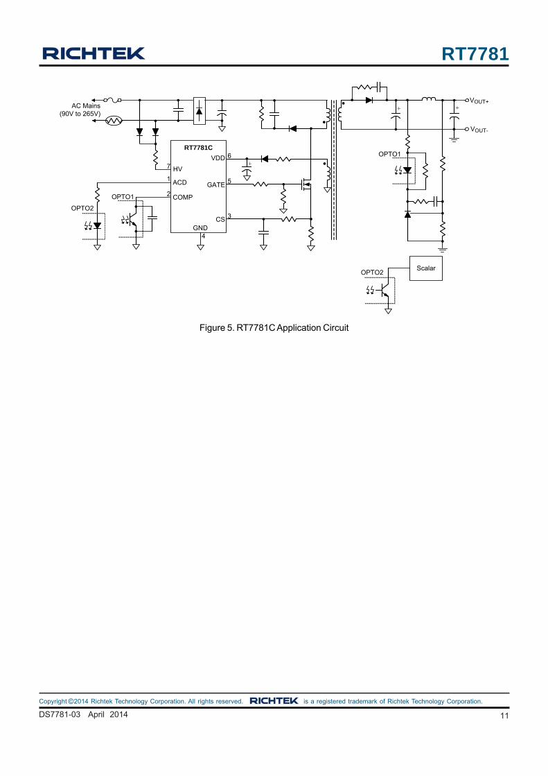
Figure 5. RT7781C Application Circuit
VOUT+
ACD
COMP
GND
VDD
GATE
CS
RT7781C
AC Mains(90V to 265V)
VOUT-
HV
2
3
4
5
6
7
1
OPTO1
OPTO1
+
++
Scalar
OPTO2
OPTO2
RT7781
12 DS7781-03 April 2014
©Copyright 2014 Richtek Technology Corporation. All rights reserved. is a registered trademark of Richtek Technology Corporation.
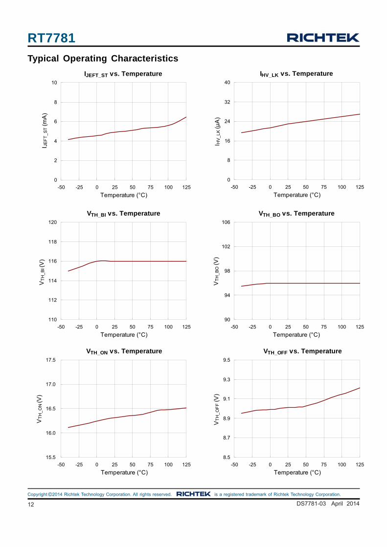
Typical Operating Characteristics
IJEFT_ST vs. Temperature
0
2
4
6
8
10
-50 -25 0 25 50 75 100 125
Temperature (°C)
I JE
FT
_S
T (
mA
)
IHV_LK vs. Temperature
0
8
16
24
32
40
-50 -25 0 25 50 75 100 125
Temperature (°C)
I HV
_L
K (μ
A)
VTH_ON vs. Temperature
15.5
16.0
16.5
17.0
17.5
-50 -25 0 25 50 75 100 125
Temperature (°C)
VT
H_
ON (
V)
VTH_OFF vs. Temperature
8.5
8.7
8.9
9.1
9.3
9.5
-50 -25 0 25 50 75 100 125
Temperature (°C)
VT
H_
OF
F (
V)
VTH_BI vs. Temperature
110
112
114
116
118
120
-50 -25 0 25 50 75 100 125
Temperature (°C)
VT
H_
BI (
V)
VTH_BO vs. Temperature
90
94
98
102
106
-50 -25 0 25 50 75 100 125
Temperature (°C)
VT
H_
BO (
V)
RT7781
13DS7781-03 April 2014
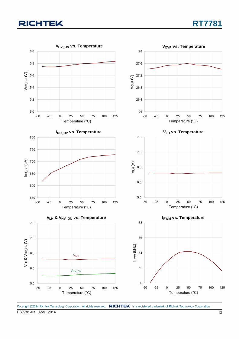
©Copyright 2014 Richtek Technology Corporation. All rights reserved. is a registered trademark of Richtek Technology Corporation.
VHV_ON vs. Temperature
5.0
5.2
5.4
5.6
5.8
6.0
-50 -25 0 25 50 75 100 125
Temperature (°C)
VH
V_
ON (
V)
VOVP vs. Temperature
26
26.4
26.8
27.2
27.6
28
-50 -25 0 25 50 75 100 125
Temperature (°C)
VO
VP (
V)
IDD_OP vs. Temperature
550
600
650
700
750
800
-50 -25 0 25 50 75 100 125
Temperature (°C)
I DD
_O
P (μ
A)
VLH vs. Temperature
5.5
6.0
6.5
7.0
7.5
-50 -25 0 25 50 75 100 125
Temperature (°C)
VL
H (
V)
VLH & VHV_ON vs. Temperature
5.5
6.0
6.5
7.0
7.5
-50 -25 0 25 50 75 100 125
Temperature (°C)
VL
H &
VH
V_
ON (
V)
fPWM vs. Temperature
60
62
64
66
68
-50 -25 0 25 50 75 100 125
Temperature (°C)
f PW
M (
kHz)
VLH
VHV_ON
RT7781
14 DS7781-03 April 2014
©Copyright 2014 Richtek Technology Corporation. All rights reserved. is a registered trademark of Richtek Technology Corporation.
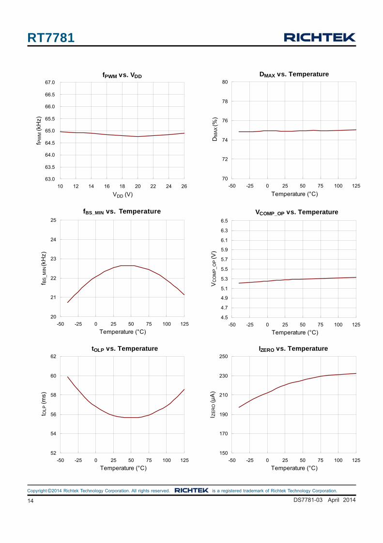
fBS_MIN vs. Temperature
20
21
22
23
24
25
-50 -25 0 25 50 75 100 125
Temperature (°C)
f BS
_M
IN (
kHz)
fPWM vs. VDD
63.0
63.5
64.0
64.5
65.0
65.5
66.0
66.5
67.0
10 12 14 16 18 20 22 24 26
VDD (V)
f PW
M (
kHz)
DMAX vs. Temperature
70
72
74
76
78
80
-50 -25 0 25 50 75 100 125
Temperature (°C)
DM
AX
(%)
VCOMP_OP vs. Temperature
4.5
4.7
4.9
5.1
5.3
5.5
5.7
5.9
6.1
6.3
6.5
-50 -25 0 25 50 75 100 125
Temperature (°C)
VC
OM
P_
OP (
V)
tOLP vs. Temperature
52
54
56
58
60
62
-50 -25 0 25 50 75 100 125
Temperature (°C)
t OL
P (
ms)
IZERO vs. Temperature
150
170
190
210
230
250
-50 -25 0 25 50 75 100 125
Temperature (°C)
I ZE
RO (μ
A)
fBS_MIN vs. Temperature
RT7781
15DS7781-03 April 2014
©Copyright 2014 Richtek Technology Corporation. All rights reserved. is a registered trademark of Richtek Technology Corporation.
VCLAMP vs. Temperature
10
11
12
13
14
15
-50 -25 0 25 50 75 100 125
Temperature (°C)
VC
LA
MP (
V)
IBIAS vs. Temperature
90
95
100
105
110
-50 -25 0 25 50 75 100 125
Temperature (°C)
I BIA
S (μ
A)
tR vs. Temperature
40
45
50
55
60
65
70
-50 -25 0 25 50 75 100 125
Temperature (°C)
t R (
ns)
tF vs. Temperature
10
20
30
40
50
60
-50 -25 0 25 50 75 100 125
Temperature (°C)
t F (
ns)
VTH_H vs. Temperature
1.70
1.75
1.80
1.85
1.90
-50 -25 0 25 50 75 100 125
Temperature (°C)
VT
H_
H (
V)
VTH_L vs. Temperature
0.20
0.25
0.30
0.35
0.40
-50 -25 0 25 50 75 100 125
Temperature (°C)
VT
H_
L (V
)
RT7781
16 DS7781-03 April 2014
©Copyright 2014 Richtek Technology Corporation. All rights reserved. is a registered trademark of Richtek Technology Corporation.
VTH_OTP vs. Temperature
0.40
0.45
0.50
0.55
0.60
-50 -25 0 25 50 75 100 125
Temperature (°C)
VT
H_
OT
P (
V)
VPRO_OP vs. Temperature
0.5
0.9
1.3
1.7
2.1
2.5
-50 -25 0 25 50 75 100 125
Temperature (°C)
VP
RO
_O
P (
V)

RT7781
17DS7781-03 April 2014
©Copyright 2014 Richtek Technology Corporation. All rights reserved. is a registered trademark of Richtek Technology Corporation.
Application Information
Start-up
The RT7781 features a HV pin to provide fast start-up.
700V start-up device is integrated in the controller to further
minimize power consumption and enhance performance.
The start-up device will be turned on during start-up and
be turned off during normal operation. It shortens start-up
time and no power loss in this path after start-up.
As shown in Figure 6, the resistor RHV connected in series
with HV pin is recommended in the range from 2kΩ to
6.6kΩ (tolerance < ±5%). If RHV is much larger than 6.6kΩ(tolerance < ±5%), the brown-in and brown-out threshold
will be inaccurate.
Brown-In and Brown-Out
The RT7781 features internal precise brown-in and brown-
out detections. An AC voltage detection circuit is built in
the controller so that the brown-in and brown-out can be
implemented without extra components. The brown-out
offers precise brown-out detection without AC ripple effect
at heavy or light load.
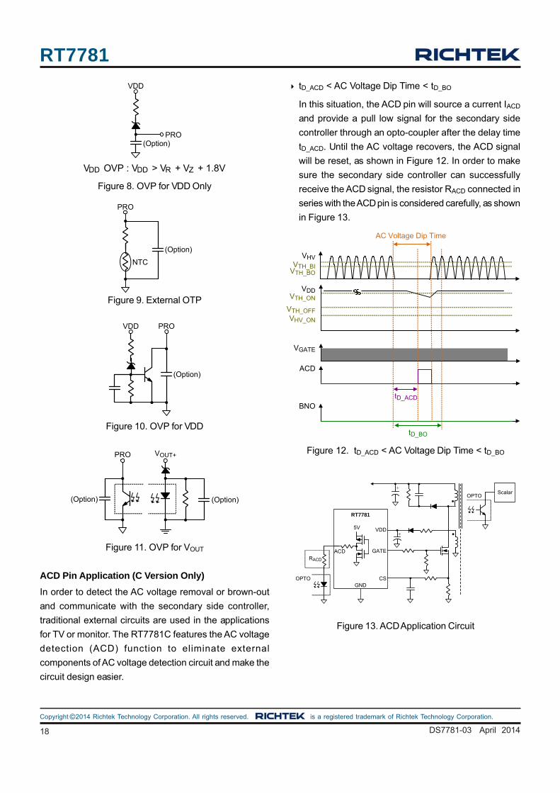
PRO Pin Application (RT7781G/L/A/T)
The RT7781 features a PRO pin for external arbitrary OVP
or OTP applications as shown in Figure 7 to Figure 11.
If the PRO pin voltage is higher than OTP threshold
VTH_OTP and is lower than pull high threshold VTH_H, the
controller is enabled for normal operation. If the PRO pin
voltage falls below VTH_OTP and is greater than pull low
COMP
GND
VDD
GATE
CS
RT7781
AC Mains(90V to 265V)
HV
2
3
4
5
6
7
OPTO
+RHV
Figure 6. Start-up Circuit
threshold VTH_L after tD_OTP de-bounce time, the controller
will shut down. Once the PRO pin voltage is higher than
VTH_H or lower than VTH_L, the controller will cease
switching and shut down after the 50μs deglitch time.
In order to pull up the PRO voltage to be above the VTH_H,
the external supply current flowing into the PRO pin must
be greater than 500μA and be limited below 5mA. When
the IC is latched at off-state by the fault latch (entering
latch-mode), VDD will be clamped at the latch-mode voltage
threshold VLH, and the fault latch will be reset when the
VDD falls and reaches the VDD reset voltage threshold
VLH_RST.
When the PRO pin is open, it is set at 1.3V internally.
Just leave the PRO pin open if it is not used. If designers
want to use a bypass capacitor on the PRO pin, the
capacitor should less than 1nF. The internal bias current
of PRO pin is 100μA (typ.).
PRO
56ms Debounce
50µsDeglitchVTH_H
50µsDeglitch
Latch+
-
+
-
+
-
VTH_OTP
VTH_L
Auto Recovery
Latch
Auto Recovery
Latch
VTH_OTP
VTH_H
VPRO
VTH_L
Auto Recovery / Latch
Normal Operating
Latch
Auto Recovery / Latch
Figure 7. PRO Functional Diagram
RT7781
18 DS7781-03 April 2014
©Copyright 2014 Richtek Technology Corporation. All rights reserved. is a registered trademark of Richtek Technology Corporation.
Figure 13. ACD Application Circuit
GND
VDD
GATE
CS
RT7781
++
5V
ACD
OPTO
RACD
ScalarOPTO
Figure 10. OVP for VDD
Figure 11. OVP for VOUT
VDD PRO
(Option)
PRO VOUT+
(Option)(Option)
ACD Pin Application (C Version Only)
In order to detect the AC voltage removal or brown-out
and communicate with the secondary side controller,
traditional external circuits are used in the applications
for TV or monitor. The RT7781C features the AC voltage
detection (ACD) function to eliminate external
components of AC voltage detection circuit and make the
circuit design easier.
Figure 12. tD_ACD < AC Voltage Dip Time < tD_BO
VGATE
VHV
VDD
AC Voltage Dip Time
tD_BO
BNO
ACD
tD_ACD
VHV_ON
VTH_ON
VTH_BIVTH_BO
VTH_OFF
Figure 8. OVP for VDD Only
VDD
PRO(Option)
DD DD R ZV OVP : V > V + V + 1.8V
Figure 9. External OTP
PRO
NTC
(Option)
tD_ACD < AC Voltage Dip Time < tD_BO
In this situation, the ACD pin will source a current IACD
and provide a pull low signal for the secondary side
controller through an opto-coupler after the delay time
tD_ACD. Until the AC voltage recovers, the ACD signal
will be reset, as shown in Figure 12. In order to make
sure the secondary side controller can successfully
receive the ACD signal, the resistor RACD connected in
series with the ACD pin is considered carefully, as shown
in Figure 13.
RT7781
19DS7781-03 April 2014
©Copyright 2014 Richtek Technology Corporation. All rights reserved. is a registered trademark of Richtek Technology Corporation.
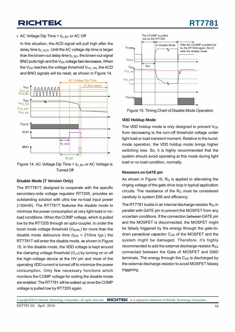
VDD Holdup Mode
The VDD holdup mode is only designed to prevent VDD
from decreasing to the turn-off threshold voltage under
light load or load transient moment. Relative to the burst-
mode operation, the VDD holdup mode brings higher
switching loss. So, it is highly recommended that the
system should avoid operating at this mode during light
load or no load condition, normally.
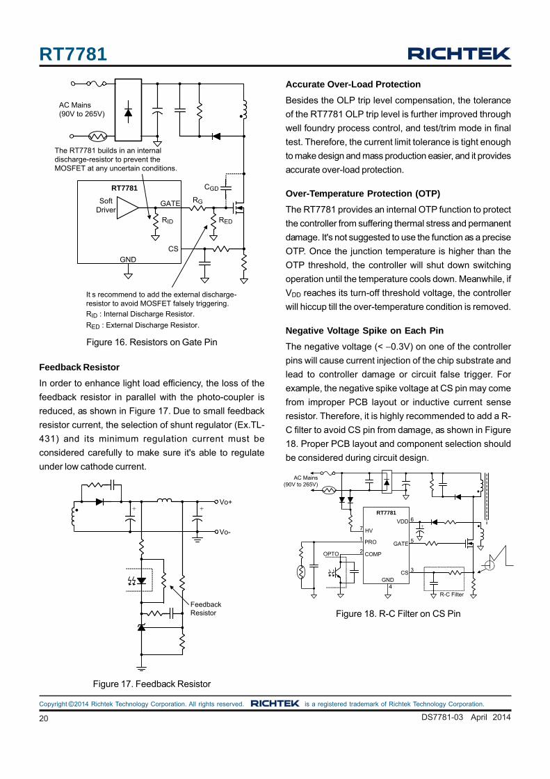
Resistors on GATE pin
As shown in Figure 16, RG is applied to alleviating the
ringing voltage of the gate drive loop in typical application
circuits. The resistance of the RG must be considered
carefully to system EMI and efficiency.
The RT7781 builds in an internal discharge-resistor RID in
parallel with GATE pin to prevent the MOSFET from any
uncertain conditions. If the connection between GATE pin
and the MOSFET is disconnected, the MOSFET might
be falsely triggered by the energy through the gate-to-
drain parasitical capacitor CGD of the MOSFET and the
system might be damaged. Therefore, it's highly
recommended to add the external discharge-resistor RED
connected between the Gate of MOSFET and GND
terminals. The energy through the CGD is discharged by
the external discharge-resistor to avoid MOSFET falsely
triggering.
Figure 15. Timing Chart of Disable Mode Operation
VCOMP
VGATE
VDD
VBURL
VTH_ON
VTH_OFF
VLH
tDIS
The VCOMP is pulled low by the RT7205
In Disable Mode After the VCOMP is pulled low by the RT7205 again, the IC exits the disable mode.
Figure 14. AC Voltage Dip Time > tD_BO or AC Voltage is
Turned Off
Disable Mode (T Version Only)
The RT7781T, designed to cooperate with the specific
secondary-side voltage regulator RT7205, provides an
outstanding solution with ultra low no-load input power
(<30mW). The RT7781T features the disable mode to
minimize the power consumption at very light-load or no-
load conditions. When the COMP voltage, which is pulled
low by the RT7205 through an opto-coupler, is under the
burst mode voltage threshold (VBURL) for more than the
disable mode debounce time (tDIS = 210ms typ.) the
RT7781T will enter the disable mode, as shown in Figure
15. In the disable mode, the VDD voltage is kept around
the clamping voltage threshold (VLH) by turning on or off
the high-voltage device at the HV pin and most of the
operating VDD current is turned off to minimize the power
consumption. Only few necessary functions which
monitors the COMP voltage for exiting the disable mode
are enabled. The RT7781 will be waked up once the COMP
voltage is pulled low by RT7205 again.
AC Voltage Dip Time > tD_BO or AC Off
In this situation, the ACD signal will pull high after the
delay time tD_ACD. Until the AC voltage dip time is larger
than the brown-out delay time tD_BO, the brown-out signal
BNO pulls high and the VDD voltage fast decreases. When
the VDD reaches the voltage threshold VHV_ON, the ACD
and BNO signals will be reset, as shown in Figure 14.
VGATE
VHV
VDD
AC Voltage Dip Time
tD_BO
BNO
ACD
IC Shut down
tD_ACD
VHV_ON
VTH_ON
VTH_BIVTH_BO
VTH_OFF
RT7781
20 DS7781-03 April 2014
©Copyright 2014 Richtek Technology Corporation. All rights reserved. is a registered trademark of Richtek Technology Corporation.
Figure 18. R-C Filter on CS Pin
Figure 17. Feedback Resistor
Accurate Over-Load Protection
Besides the OLP trip level compensation, the tolerance
of the RT7781 OLP trip level is further improved through
well foundry process control, and test/trim mode in final
test. Therefore, the current limit tolerance is tight enough
to make design and mass production easier, and it provides
accurate over-load protection.
Over-Temperature Protection (OTP)
The RT7781 provides an internal OTP function to protect
the controller from suffering thermal stress and permanent
damage. It's not suggested to use the function as a precise
OTP. Once the junction temperature is higher than the
OTP threshold, the controller will shut down switching
operation until the temperature cools down. Meanwhile, if
VDD reaches its turn-off threshold voltage, the controller
will hiccup till the over-temperature condition is removed.
Negative Voltage Spike on Each Pin
The negative voltage (< −0.3V) on one of the controller
pins will cause current injection of the chip substrate and
lead to controller damage or circuit false trigger. For
example, the negative spike voltage at CS pin may come
from improper PCB layout or inductive current sense
resistor. Therefore, it is highly recommended to add a R-
C filter to avoid CS pin from damage, as shown in Figure
18. Proper PCB layout and component selection should
be considered during circuit design.
Feedback Resistor
In order to enhance light load efficiency, the loss of the
feedback resistor in parallel with the photo-coupler is
reduced, as shown in Figure 17. Due to small feedback
resistor current, the selection of shunt regulator (Ex.TL-
431) and its minimum regulation current must be
considered carefully to make sure it's able to regulate
under low cathode current.
Figure 16. Resistors on Gate Pin
AC Mains(90V to 265V)
GND
GATE
CS
RT7781
RG
RED
CGD
RID
SoftDriver
It s recommend to add the external discharge-resistor to avoid MOSFET falsely triggering.
RID : Internal Discharge Resistor.
RED : External Discharge Resistor.
The RT7781 builds in an internal discharge-resistor to prevent the MOSFET at any uncertain conditions.
COMP
GND
VDD
GATE
CS
RT7781
AC Mains(90V to 265V)
HV
2
3
4
5
6
7
OPTO
+
PRO1
R-C Filter
+ + Vo+
Vo-
Feedback Resistor
RT7781
21DS7781-03 April 2014
©Copyright 2014 Richtek Technology Corporation. All rights reserved. is a registered trademark of Richtek Technology Corporation.
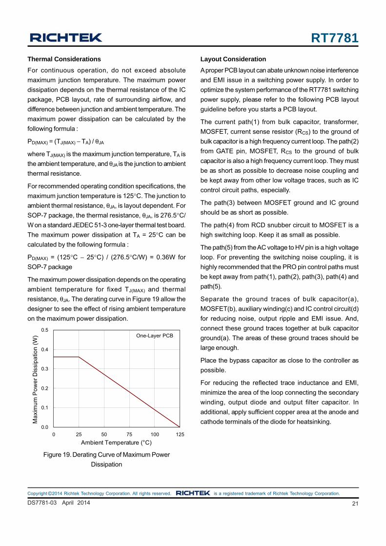
Thermal Considerations
For continuous operation, do not exceed absolute
maximum junction temperature. The maximum power
dissipation depends on the thermal resistance of the IC
package, PCB layout, rate of surrounding airflow, and
difference between junction and ambient temperature. The
maximum power dissipation can be calculated by the
following formula :
PD(MAX) = (TJ(MAX) − TA) / θJA
where TJ(MAX) is the maximum junction temperature, TA is
the ambient temperature, and θJA is the junction to ambient
thermal resistance.
For recommended operating condition specifications, the
maximum junction temperature is 125°C. The junction to
ambient thermal resistance, θJA, is layout dependent. For
SOP-7 package, the thermal resistance, θJA, is 276.5°C/
W on a standard JEDEC 51-3 one-layer thermal test board.
The maximum power dissipation at TA = 25°C can be
calculated by the following formula :
PD(MAX) = (125°C − 25°C) / (276.5°C/W) = 0.36W for
SOP-7 package
The maximum power dissipation depends on the operating
ambient temperature for fixed TJ(MAX) and thermal
resistance, θJA. The derating curve in Figure 19 allow the
designer to see the effect of rising ambient temperature
on the maximum power dissipation.
Figure 19. Derating Curve of Maximum Power
Dissipation
0.0
0.1
0.2
0.3
0.4
0.5
0 25 50 75 100 125
Ambient Temperature (°C)
Ma
xim
um
Po
we
r D
issi
pa
tion
(W
) 1 One-Layer PCB
Layout Consideration
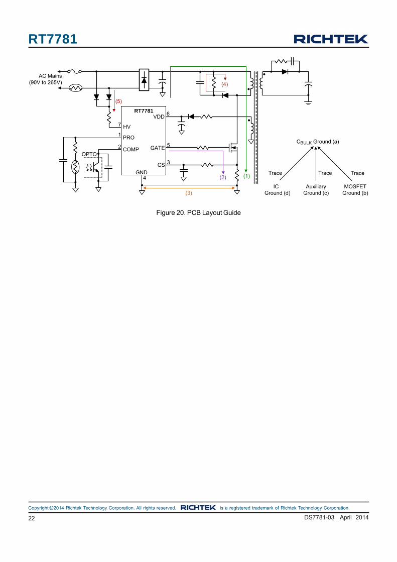
A proper PCB layout can abate unknown noise interference
and EMI issue in a switching power supply. In order to
optimize the system performance of the RT7781 switching
power supply, please refer to the following PCB layout
guideline before you starts a PCB layout.
The current path(1) from bulk capacitor, transformer,
MOSFET, current sense resistor (RCS) to the ground of
bulk capacitor is a high frequency current loop. The path(2)
from GATE pin, MOSFET, RCS to the ground of bulk
capacitor is also a high frequency current loop. They must
be as short as possible to decrease noise coupling and
be kept away from other low voltage traces, such as IC
control circuit paths, especially.
The path(3) between MOSFET ground and IC ground
should be as short as possible.
The path(4) from RCD snubber circuit to MOSFET is a
high switching loop. Keep it as small as possible.
The path(5) from the AC voltage to HV pin is a high voltage
loop. For preventing the switching noise coupling, it is
highly recommended that the PRO pin control paths must
be kept away from path(1), path(2), path(3), path(4) and
path(5).
Separate the ground traces of bulk capacitor(a),
MOSFET(b), auxiliary winding(c) and IC control circuit(d)
for reducing noise, output ripple and EMI issue. And,
connect these ground traces together at bulk capacitor
ground(a). The areas of these ground traces should be
large enough.
Place the bypass capacitor as close to the controller as
possible.
For reducing the reflected trace inductance and EMI,
minimize the area of the loop connecting the secondary
winding, output diode and output filter capacitor. In
additional, apply sufficient copper area at the anode and
cathode terminals of the diode for heatsinking.
RT7781
22 DS7781-03 April 2014
©Copyright 2014 Richtek Technology Corporation. All rights reserved. is a registered trademark of Richtek Technology Corporation.
Figure 20. PCB Layout Guide
PRO
COMP
GND
VDD
GATE
CS
RT7781
AC Mains(90V to 265V)
HV
2
3
4
5
6
7
1
(1)(2)
(3)
(4)
(5)
OPTO
Auxiliary Ground (c)
IC Ground (d)
Trace Trace Trace
MOSFETGround (b)
CBULK Ground (a)
RT7781
23DS7781-03 April 2014
Richtek Technology Corporation14F, No. 8, Tai Yuen 1st Street, Chupei City
Hsinchu, Taiwan, R.O.C.
Tel: (8863)5526789
Richtek products are sold by description only. Richtek reserves the right to change the circuitry and/or specifications without notice at any time. Customers should
obtain the latest relevant information and data sheets before placing orders and should verify that such information is current and complete. Richtek cannot
assume responsibility for use of any circuitry other than circuitry entirely embodied in a Richtek product. Information furnished by Richtek is believed to be
accurate and reliable. However, no responsibility is assumed by Richtek or its subsidiaries for its use; nor for any infringements of patents or other rights of third
parties which may result from its use. No license is granted by implication or otherwise under any patent or patent rights of Richtek or its subsidiaries.
Outline Dimension
7-Lead SOP Plastic Package
Min. Max. Min. Max.
A 4.801 5.004 0.189 0.197
B 3.810 3.988 0.150 0.157
C 1.346 1.753 0.053 0.069
D 0.310 0.510 0.012 0.020
F 1.194 1.346 0.047 0.053
F1 2.464 2.616 0.097 0.103
H 0.100 0.254 0.004 0.010
I 0.050 0.254 0.002 0.010
J 5.791 6.200 0.228 0.244
M 0.400 1.270 0.016 0.050
SymbolDimensions In Millimeters Dimensions In Inches