Embed Size (px)
Citation preview
17TH INTERNATIONAL TRAVELLING SUMMER SCHOOL ON MICROWAVES & LIGHTWAVES, Pforzheim, July 7-13, 2007
Precise Microwave Vector Measurements
Karel Hoffmann
Czech Technical University in Prague Faculty of Electrical Engineering
Department of Electromagnetic Field Technická 2, 162 00 Prague 6, Czech Republic
Tel.: (+420) 224 352 276 Fax: (+420) 233 339 958
E-mail: [email protected]
Czech Technical University in Prague, Czech Republic
17TH INTERNATIONAL TRAVELLING SUMMER SCHOOL ON MICROWAVES & LIGHTWAVES, Pforzheim, July 7-13, 2007
Content
- Introduction - Vector measurements of single-ended devices - Vector measurements of multiport devices
- Vector measurements of differential devices - Conclusion
Acknowledgement This work has been supported by research program No. MSM6840770015 "Research of Methods and Systems for Measurement of Physical Quantities and Measured Data Processing " of the CTU in Prague sponsored by the Ministry of Education, Youth and Sports of the Czech Republic.
Czech Technical University in Prague, Czech Republic
17TH INTERNATIONAL TRAVELLING SUMMER SCHOOL ON MICROWAVES & LIGHTWAVES, Pforzheim, July 7-13, 2007
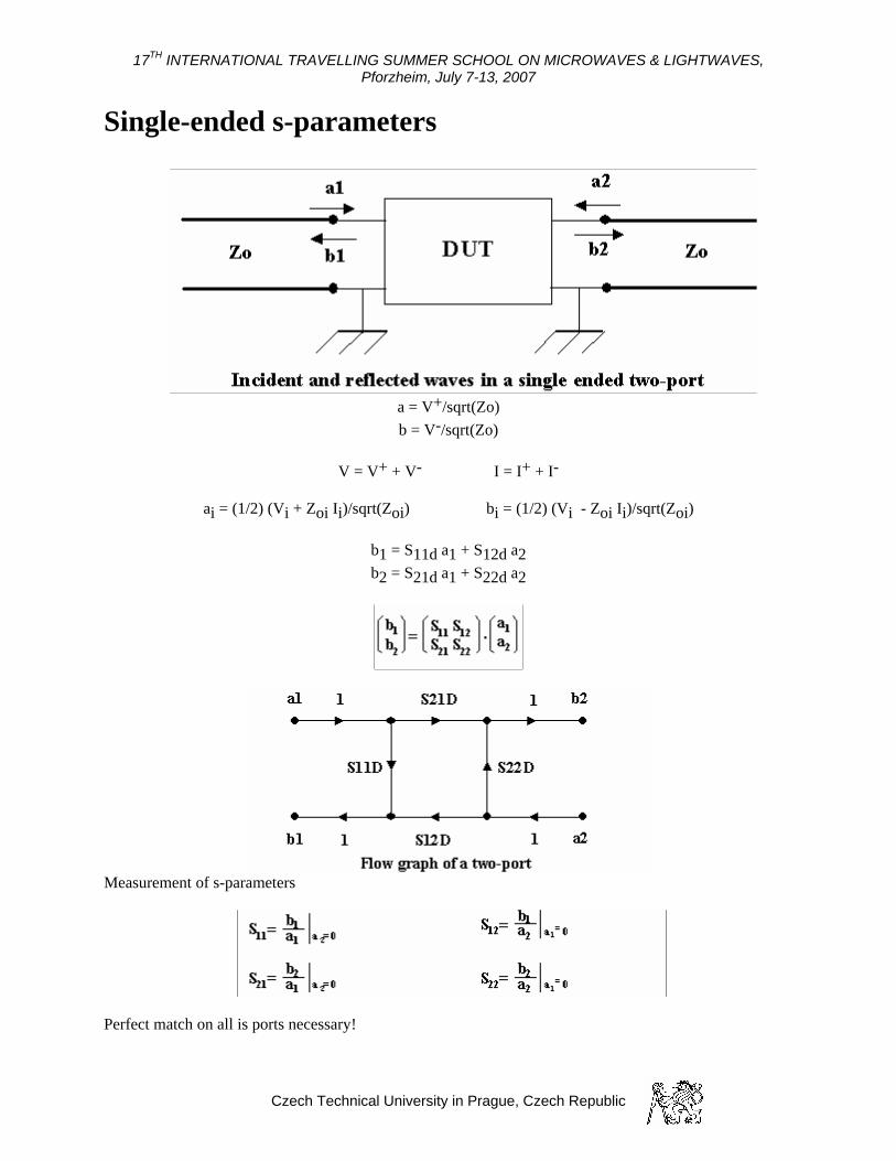
Single-ended s-parameters
a = V+/sqrt(Zo) b = V-/sqrt(Zo)
V = V+ + V- I = I+ + I-
ai = (1/2) (Vi + Zoi Ii)/sqrt(Zoi) bi = (1/2) (Vi - Zoi Ii)/sqrt(Zoi)
b1 = S11d a1 + S12d a2 b2 = S21d a1 + S22d a2
Measurement of s-parameters
Perfect match on all is ports necessary!
Czech Technical University in Prague, Czech Republic
17TH INTERNATIONAL TRAVELLING SUMMER SCHOOL ON MICROWAVES & LIGHTWAVES, Pforzheim, July 7-13, 2007
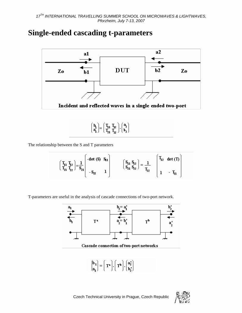
Single-ended cascading t-parameters
The relationship between the S and T parameters
T-parameters are useful in the analysis of cascade connections of two-port network.
Czech Technical University in Prague, Czech Republic
17TH INTERNATIONAL TRAVELLING SUMMER SCHOOL ON MICROWAVES & LIGHTWAVES, Pforzheim, July 7-13, 2007
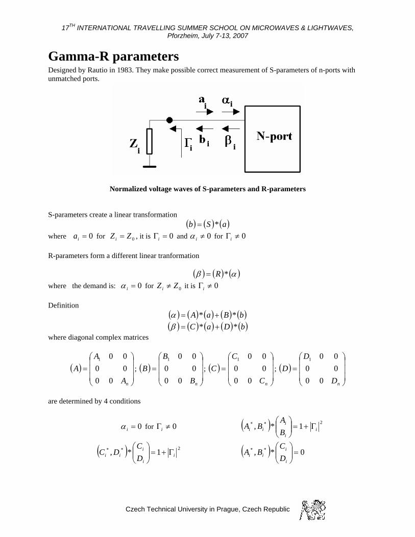
Gamma-R parameters ible correct measurement of S-parameters of n-ports with
-parameters create a linear transformation
Designed by Rautio in 1983. They make possunmatched ports.
Normalized voltage waves of S-parameters and R-parameters
S( ) ( ) ( )aSb *=
where 0=a for ZZ = , it is 0=Γ ai 0i ndi 0≠iα for 0≠Γi
different linear tranformation R-parameters form a
( ) ( ) ( )α*Rβ = where the demand is: 0=iα for ≠ it is 0i ZZ 0≠Γi Definition
( ) ( ) ( ) ( ) ( )bBaA ** +=α ( ) ( ) ( ) ( ) ( )bDaC ** +=β
where diagonal complex matrices
⎠⎜⎜
⎝
=
nAA
0000
are determined by 4 conditions
( )⎟⎟⎟⎞
⎜⎛ A 001
; ( )⎟⎟⎟
⎠
⎞
⎜⎜⎜
⎝
⎛=
nB
BB
0000001
; ( )⎟⎟⎟
⎠
⎞
⎜⎜⎜
⎝
⎛=
nC
CC
0000001
; ( )⎟⎟⎟
⎠
⎞
⎜⎜⎜
⎝
⎛=
nD
DD
0000001
0=iα for 0≠Γi ( ) 21*, ii
iii B
ABA Γ+=⎟⎟
⎠
⎞⎜⎜⎝
⎛∗∗
( ) 2i =⎟⎞
1*, ii
ii DC
DC Γ+⎟⎠
⎜⎜⎝
⎛∗∗
( ) 0*, =⎟⎟⎠
⎞⎜⎜⎝
⎛∗∗
i
iii D
CBA
Czech Technical University in Prague, Czech Republic
17TH INTERNATIONAL TRAVELLING SUMMER SCHOOL ON MICROWAVES & LIGHTWAVES, Pforzheim, July 7-13, 2007
It yields
; ( ) ( ) ( ) ( )ba +Γ= ∗ *β ( ) ( ) ( ) ( )ba *Γ−=αwhere
1
is the diagonal matrix of nonzero reflection coefficients of impedances connected on individual ports of
e n-port.
( )⎟⎟⎟
⎠
⎞
⎜⎜⎜
⎝
⎛
Γ
Γ=Γ
n000000
thTranformation between S an R parameters
( ) ([ ) ( )] ([ ) ( ) ( )] 1*1* −∗ Γ−+ SS Γ=R
( ) ( ) ( ) ( )[ ] ( ) ( )[ ]∗− Γ−Γ+= RRS **1 1
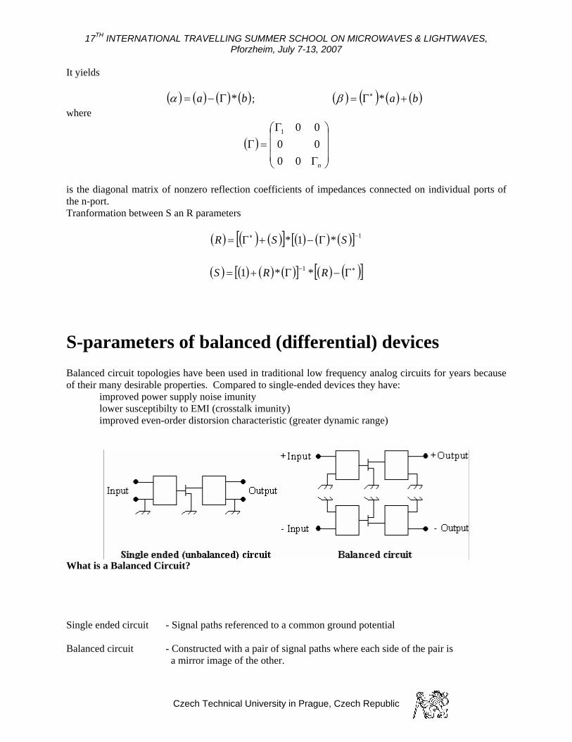
-parameters of balanced (differential) devices years because
f their many desirable properties. Compared to single-ended devices they have:
eristic (greater dynamic range)
ingle ended circuit - Signal paths referenced to a common ground potential
of the pair is a mirror image of the other.
S Balanced circuit topologies have been used in traditional low frequency analog circuits foro improved power supply noise imunity lower susceptibilty to EMI (crosstalk imunity) improved even-order distorsion charact
What is a Balanced Circuit?
S Balanced circuit - Constructed with a pair of signal paths where each side
Czech Technical University in Prague, Czech Republic
17TH INTERNATIONAL TRAVELLING SUMMER SCHOOL ON MICROWAVES & LIGHTWAVES, Pforzheim, July 7-13, 2007
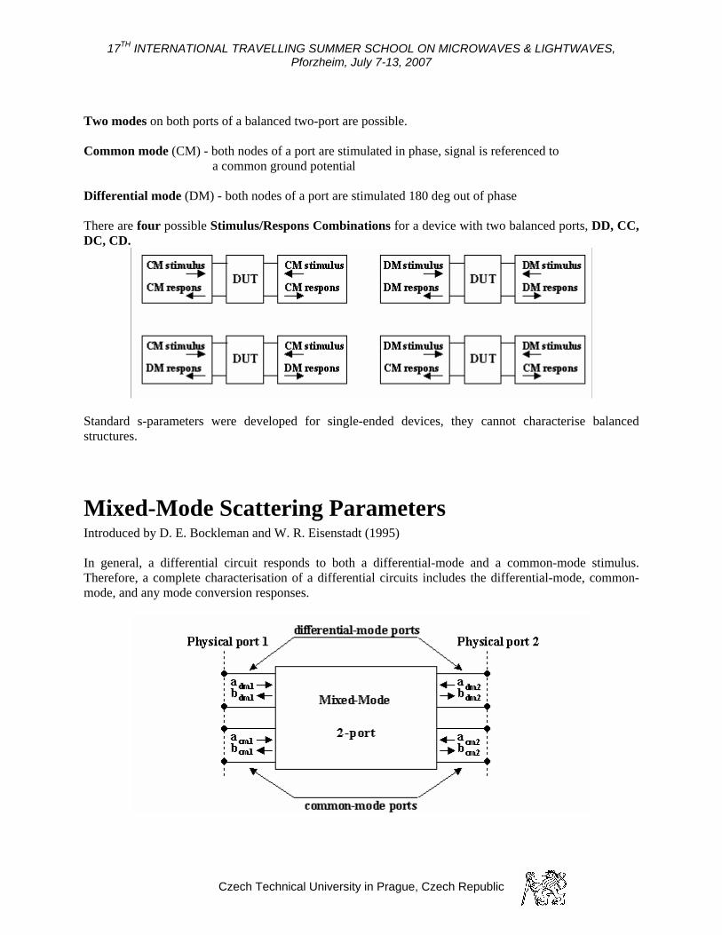
Two modes on both ports of a balanced two-port are possible.
ase, signal is referenced to a common ground potential
mulated 180 deg out of phase
anced ports, DD, CC, C, CD.
se balanced
tructures.
ixed-Mode Scattering Parameters
ntial-mode and a common-mode stimulus. herefore, a complete characterisation of a differential circuits includes the differential-mode, common-
Common mode (CM) - both nodes of a port are stimulated in ph Differential mode (DM) - both nodes of a port are sti There are four possible Stimulus/Respons Combinations for a device with two balD
Standard s-parameters were developed for single-ended devices, they cannot characteris
MIntroduced by D. E. Bockleman and W. R. Eisenstadt (1995) In general, a differential circuit responds to both a differeTmode, and any mode conversion responses.
Czech Technical University in Prague, Czech Republic
17TH INTERNATIONAL TRAVELLING SUMMER SCHOOL ON MICROWAVES & LIGHTWAVES, Pforzheim, July 7-13, 2007
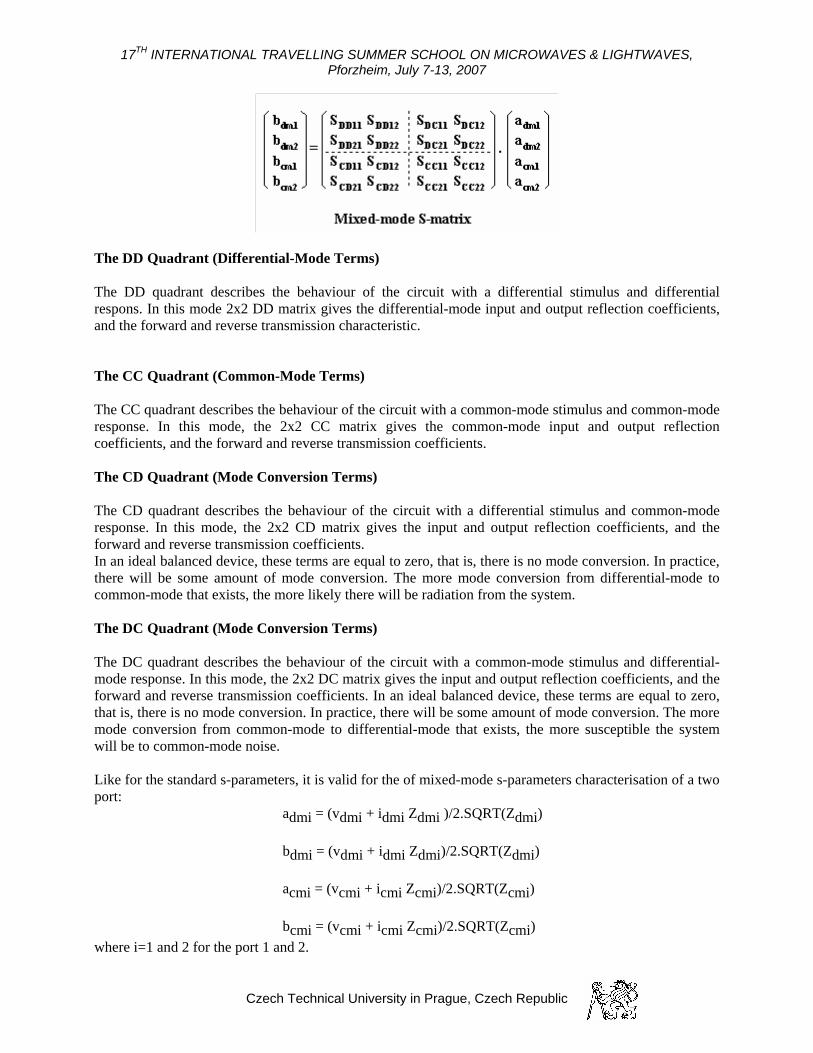
The DD Quadrant (Differential-Mode Terms) The DD quadrant describes the behaviour of the circuit with a differential stimulus and differential respons. In this mode 2x2 DD matrix gives the differential-mode input and output reflection coefficients, nd the forward and reverse transmission characteristic.
The CC The CC quadrant describes mulus and common-mode response. In this m ode input and output reflection coefficients, The CD Quadrant (Mode Conversion Ter
circuit with a differential stimulus and common-mode es the input and output reflection coefficients, and the
adiation from the system.
)
mount of mode conversion. The more ntial-mode that exists, the more susceptible the system
i Zcmi)/2.SQRT(Zcmi)
a
Quadrant (Common-Mode Terms)
the behaviour of the circuit with a common-mode stiode, the 2x2 CC matrix gives the common-m
and the forward and reverse transmission coefficients.
ms) The CD quadrant describes the behaviour of theesponse. In this mode, the 2x2 CD matrix givr
forward and reverse transmission coefficients. In an ideal balanced device, these terms are equal to zero, that is, there is no mode conversion. In practice, there will be some amount of mode conversion. The more mode conversion from differential-mode to ommon-mode that exists, the more likely there will be rc
The DC Quadrant (Mode Conversion Terms The DC quadrant describes the behaviour of the circuit with a common-mode stimulus and differential-mode response. In this mode, the 2x2 DC matrix gives the input and output reflection coefficients, and the forward and reverse transmission coefficients. In an ideal balanced device, these terms are equal to zero, hat is, there is no mode conversion. In practice, there will be some at
mode conversion from common-mode to differeill be to common-mode noise. w
Like for the standard s-parameters, it is valid for the of mixed-mode s-parameters characterisation of a two port: admi = (vdmi + idmi Zdmi )/2.SQRT(Zdmi) bdmi = (vdmi + idmi Zdmi)/2.SQRT(Zdmi) acmi = (vcmi + icm bcmi = (vcmi + icmi Zcmi)/2.SQRT(Zcmi) where i=1 and 2 for the port 1 and 2.
Czech Technical University in Prague, Czech Republic
17TH INTERNATIONAL TRAVELLING SUMMER SCHOOL ON MICROWAVES & LIGHTWAVES, Pforzheim, July 7-13, 2007
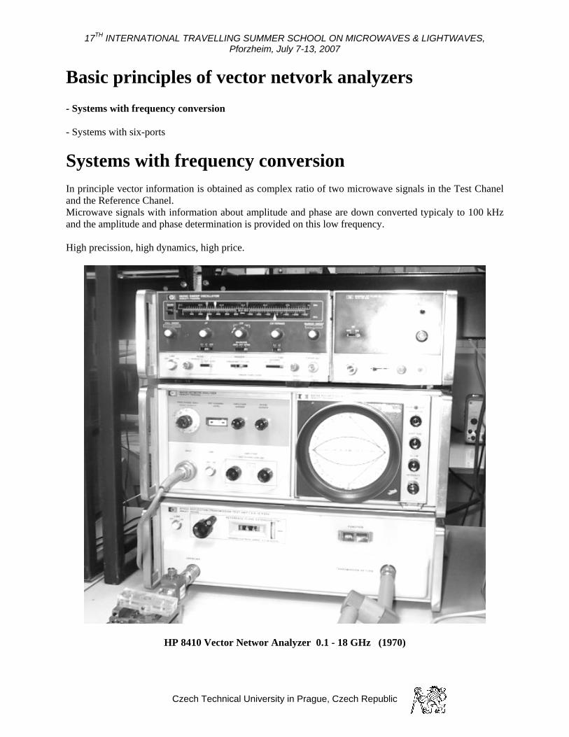
Basic principles of vector netvork analyzers - Systems with frequency conversion
ignals in the Test Chanel
onverted typicaly to 100 kHz e and phase determination is provided on this low frequency.
rice.
HP 8410 Vector Networ Analyzer 0.1 - 18 GHz (1970)
- Systems with six-ports
Systems with frequency conversion
or information is obtained as complex ratio of two microwave sIn principle vectand the Reference Chanel. Microwave signals with information about amplitude and phase are down cand the amplitud High precission, high dynamics, high p
Czech Technical University in Prague, Czech Republic
17TH INTERNATIONAL TRAVELLING SUMMER SCHOOL ON MICROWAVES & LIGHTWAVES, Pforzheim, July 7-13, 2007
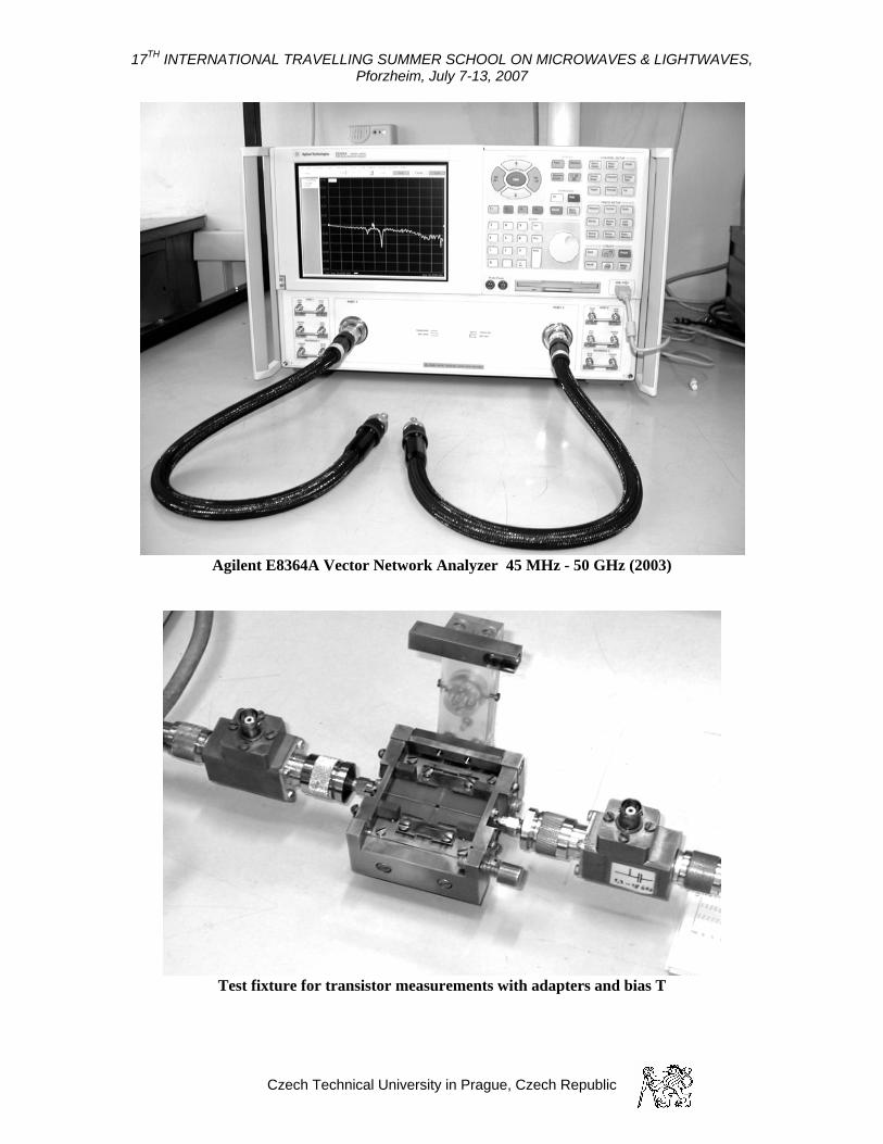
Agilent E8364A Vector Network Analyzer 45 MHz - 50 GHz (2003)
Test fixture for transistor measurements with adapters and bias T
Czech Technical University in Prague, Czech Republic
17TH INTERNATIONAL TRAVELLING SUMMER SCHOOL ON MICROWAVES & LIGHTWAVES, Pforzheim, July 7-13, 2007
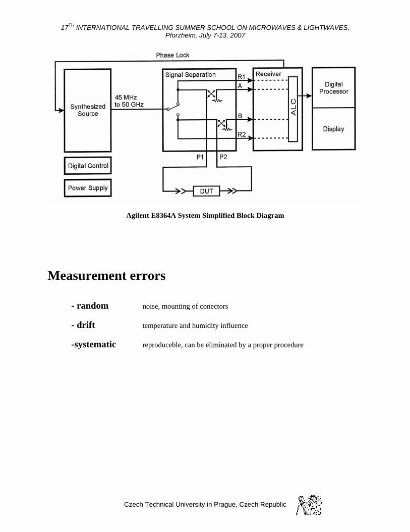
Agilent E8364A System Simplified Block Diagram
Measurement errors - random noise, mounting of conectors - drift temperature and humidity influence -systematic reproduceble, can be eliminated by a proper procedure
Czech Technical University in Prague, Czech Republic
17TH INTERNATIONAL TRAVELLING SUMMER SCHOOL ON MICROWAVES & LIGHTWAVES, Pforzheim, July 7-13, 2007
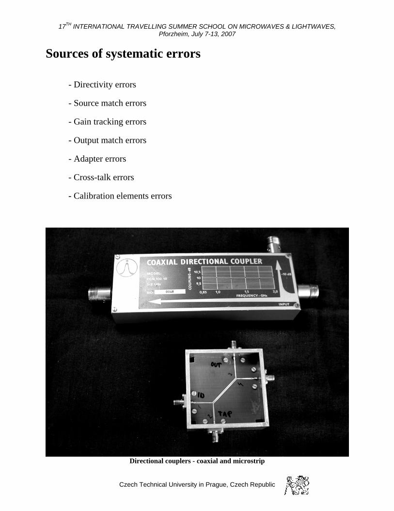
Sources of systematic errors - Directivity errors - Source match errors - Gain tracking errors - Output match errors - Adapter errors
- Cross-talk errors - Calibration elements errors
Directional couplers - coaxial and microstrip
Czech Technical University in Prague, Czech Republic
17TH INTERNATIONAL TRAVELLING SUMMER SCHOOL ON MICROWAVES & LIGHTWAVES, Pforzheim, July 7-13, 2007
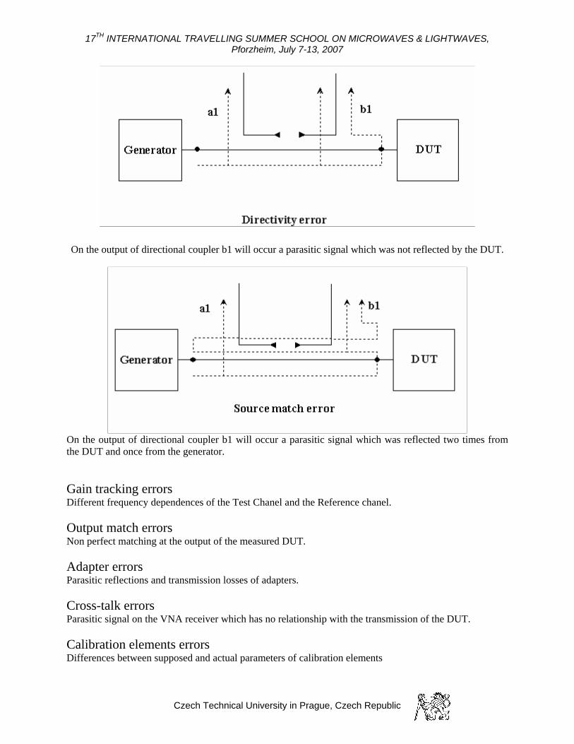
On the pler b1 will occur a parasitic signal which was not reflected by the DUT.
On the output of directional coupler b1 will occur a parasitic signal which was reflected two times from the DUT and once from the generator.
Gain tracking errors Different frequency dependences of the Test Chanel and the Reference chanel. Output match errors Non perfect matching at the output of the measured DUT. Adapter errors Parasitic reflections and transmission losses of adapters. Cross-talk errors Parasitic signal on the VNA receiver which has no relationship with the transmission of the DUT. Calibration elements errors Differences between supposed and actual parameters of calibration elements
output of directional cou
Czech Technical University in Prague, Czech Republic
17TH INTERNATIONAL TRAVELLING SUMMER SCHOOL ON MICROWAVES & LIGHTWAVES, Pforzheim, July 7-13, 2007
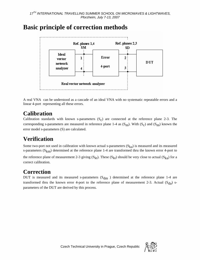
Basic principle of correction methods
A real VNA can be understood as a cascade of an ideal VNA with no systematic repeatable errors and a linear 4-port representing all these errors.
Calibration Calibration standards with known s-parameters (Sc) are connected at the reference plane 2-3. The corresponding s-parameters are measured in reference plane 1-4 as (Sm). With (Sc) and (Sm) known the error model s-parameters (S) are calculated.
Verification Some two-port not used in calibration with known actual s-parameters (Ska) is measured and its measured s-parameters (Skm) determined at the reference plane 1-4 are transformed thru the known error 4-port to
the reference plane of measurement 2-3 giving (Skt). These (Skt) should be very close to actual (Ska) for a correct calibration.
Correction DUT is measured and its measured s-parameters (Sdm ) determined at the reference plane 1-4 are transformed thru the known error 4-port to the reference plane of measurement 2-3. Actual (Sda) s-parameters of the DUT are derived by this process.
Czech Technical University in Prague, Czech Republic
17TH INTERNATIONAL TRAVELLING SUMMER SCHOOL ON MICROWAVES & LIGHTWAVES, Pforzheim, July 7-13, 2007
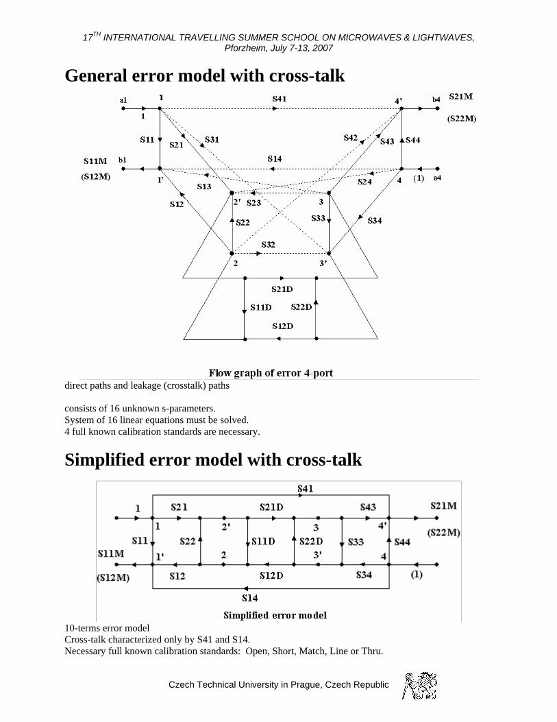
General error model with cross-talk
e (crosstalk) paths
ystem of 16 linear equations must be solved. re necessary.
10-terms error model Cross-talk characterized only by S41 and S14. Necessary full known calibration standards: Open, Short, Match, Line or Thru.
direct paths and leakag consists of 16 unknown s-parameters. S4 full known calibration standards a
Simplified error model with cross-talk
Czech Technical University in Prague, Czech Republic
17TH INTERNATIONAL TRAVELLING SUMMER SCHOOL ON MICROWAVES & LIGHTWAVES, Pforzheim, July 7-13, 2007
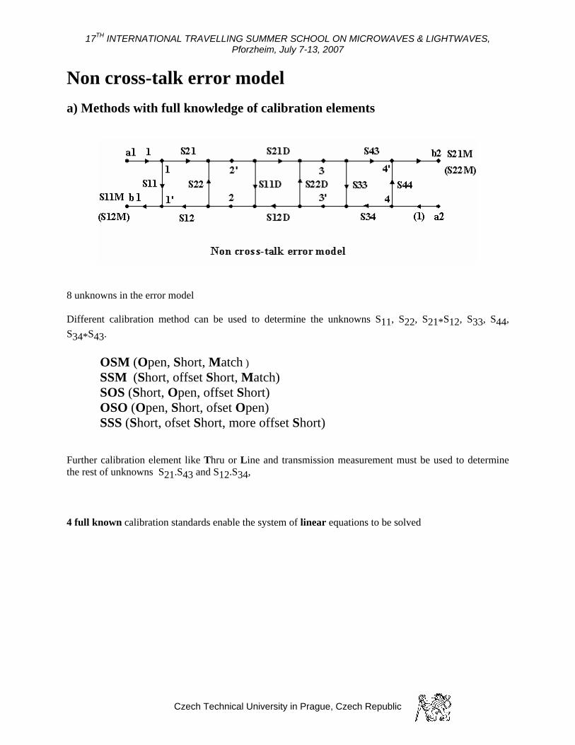
Non cross-talk error model a) Methods with full knowledge of calibration elements
ror model
OSM (Open, Short, Match ) t, offset Short, Match)
element like Thru or Line and transmission measurement must be used to determine S21.S43 and S12.S34,
of linear equations to be solved
8 unknowns in the er Different calibration method can be used to determine the unknowns S11, S22, S21*S12, S33, S44, S34*S43. SSM (Shor SOS (Short, Open, offset Short) OSO (Open, Short, ofset Open) SSS (Short, ofset Short, more offset Short) Further calibrationthe rest of unknowns
full known calibration standards enable the system4
Czech Technical University in Prague, Czech Republic
17TH INTERNATIONAL TRAVELLING SUMMER SCHOOL ON MICROWAVES & LIGHTWAVES, Pforzheim, July 7-13, 2007
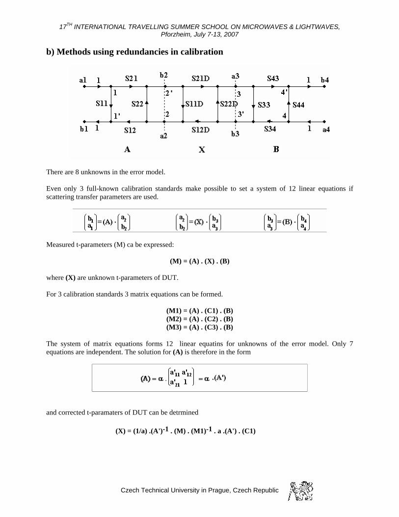
b) Methods using redundancies in calibration
There are 8 unknowns in the error model. Even only 3 full-known calibration standards make possible to set a system of 12 linear equations if scattering transfer parameters are used.
Measured t-parameters (M) ca be expressed:
DUT.
be formed.
(M3) = (A) . (C3) . (B) The system of matrix equations forms 12 linear equatins for unknowns of the error model. Only 7 equations are independent. The solution for (A) is therefore in the form
and corrected t-paramaters of DUT can be detrmined
(X) = (1/a) .(A')-1 . (M) . (M1)-1 . a .(A') . (C1)
(M) = (A) . (X) . (B) where (X) are unknown t-parameters of For 3 calibration standards 3 matrix equations can
(M1) = (A) . (C1) . (B) (M2) = (A) . (C2) . (B)
Czech Technical University in Prague, Czech Republic
17TH INTERNATIONAL TRAVELLING SUMMER SCHOOL ON MICROWAVES & LIGHTWAVES, Pforzheim, July 7-13, 2007
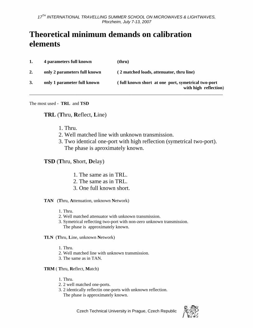
Theoretical minimum demands on calibration
. 4 parameters full known (thru) 2. only 2 parameters full known ( 2 matched loads, attenuator, thru line) 3. only 1 parameter full known ( full known short at one port, symetrical two-port
with high reflection) _____________________________________________________________________________________ The most used - TRL and TSD TRL (Thru, Reflect, Line)
ith unknown transmission.
The phase is aproximately known.
L. L.
2. Well matched attenuator with unknown transmission. 3. Symetrical reflecting two-port with non-zero unknown transmission.
TLN (Thru, Line, unknown Network)
1. Thru. 2. Well matched line with unknown transmission. 3. The same as in TAN.
TRM ( Thru, Reflect, Match)
1. Thru. 2. 2 well matched one-ports. 3. 2 identically reflectin one-ports with unknown reflection. The phase is approximately known.
elements
1
1. Thru.
2. Well matched line w 3. Two identical one-port with high reflection (symetrical two-port). TSD (Thru, Short, Delay) 1. The same as in TR 2. The same as in TR 3. One full known short.
TAN (Thru, Attenuation, unknown Network) 1. Thru.
The phase is approximately known.
Czech Technical University in Prague, Czech Republic
17TH INTERNATIONAL TRAVELLING SUMMER SCHOOL ON MICROWAVES & LIGHTWAVES, Pforzheim, July 7-13, 2007
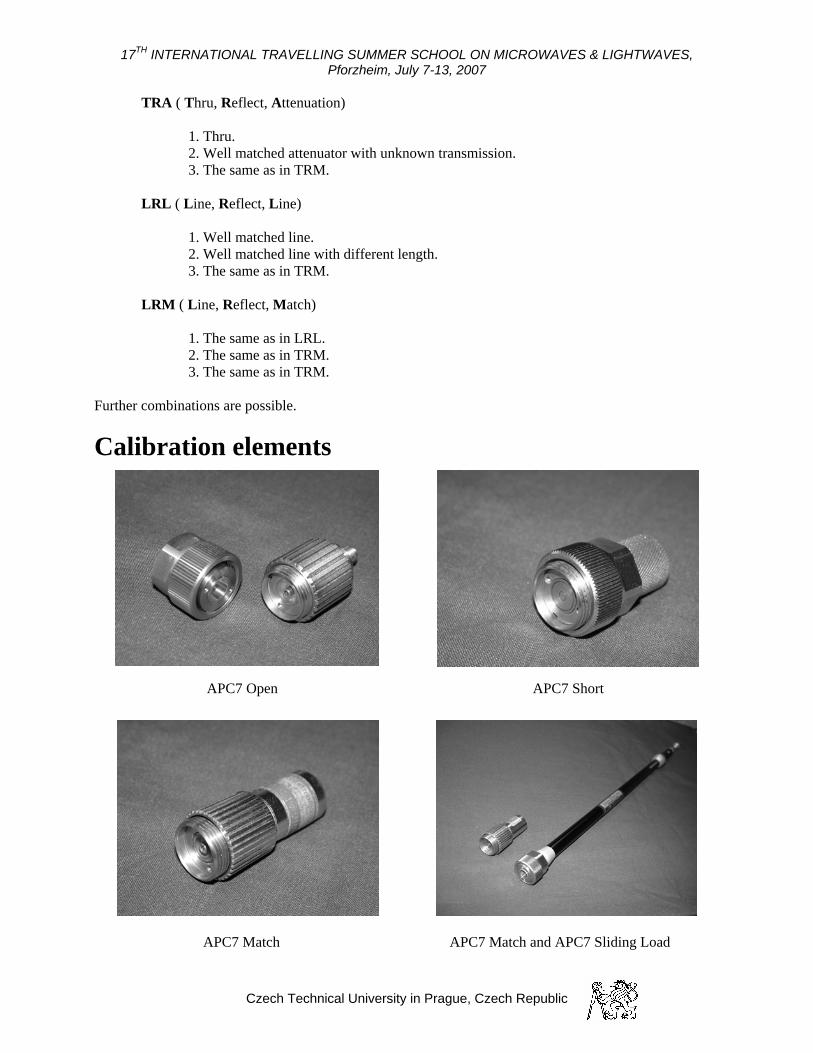
TRA ( Thru, Reflect, Attenuation) 1. Thru. 2. Well matched attenuator with unknown transmission. 3. The same as in TRM. LRL ( Line, Reflect, Line) 1. Well matched line. 2. Well matched line with different length. 3. The same as in TRM. LRM ( Line, Reflect, Match) 1. The same as in LRL.
3. The same as in TRM.
Calibration elements
APC7 Open APC7 Short
APC7 Match APC7 Match and APC7 Sliding Load
2. The same as in TRM. Further combinations are possible.
Czech Technical University in Prague, Czech Republic
17TH INTERNATIONAL TRAVELLING SUMMER SCHOOL ON MICROWAVES & LIGHTWAVES, Pforzheim, July 7-13, 2007
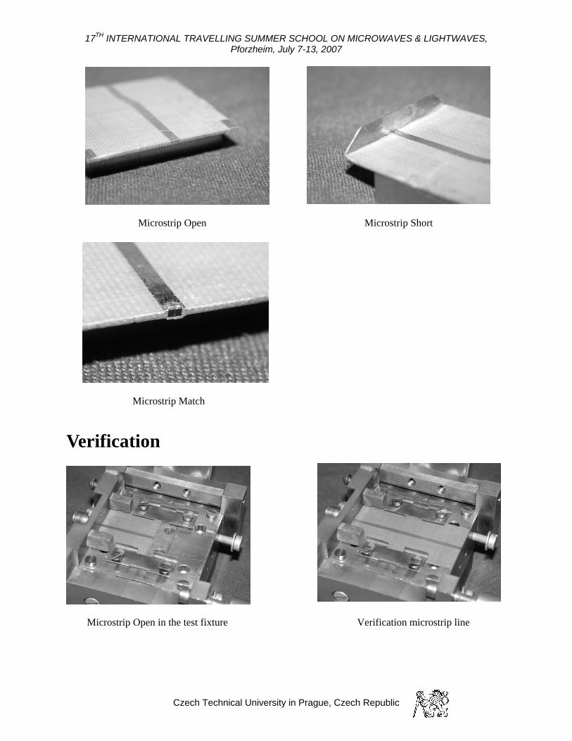
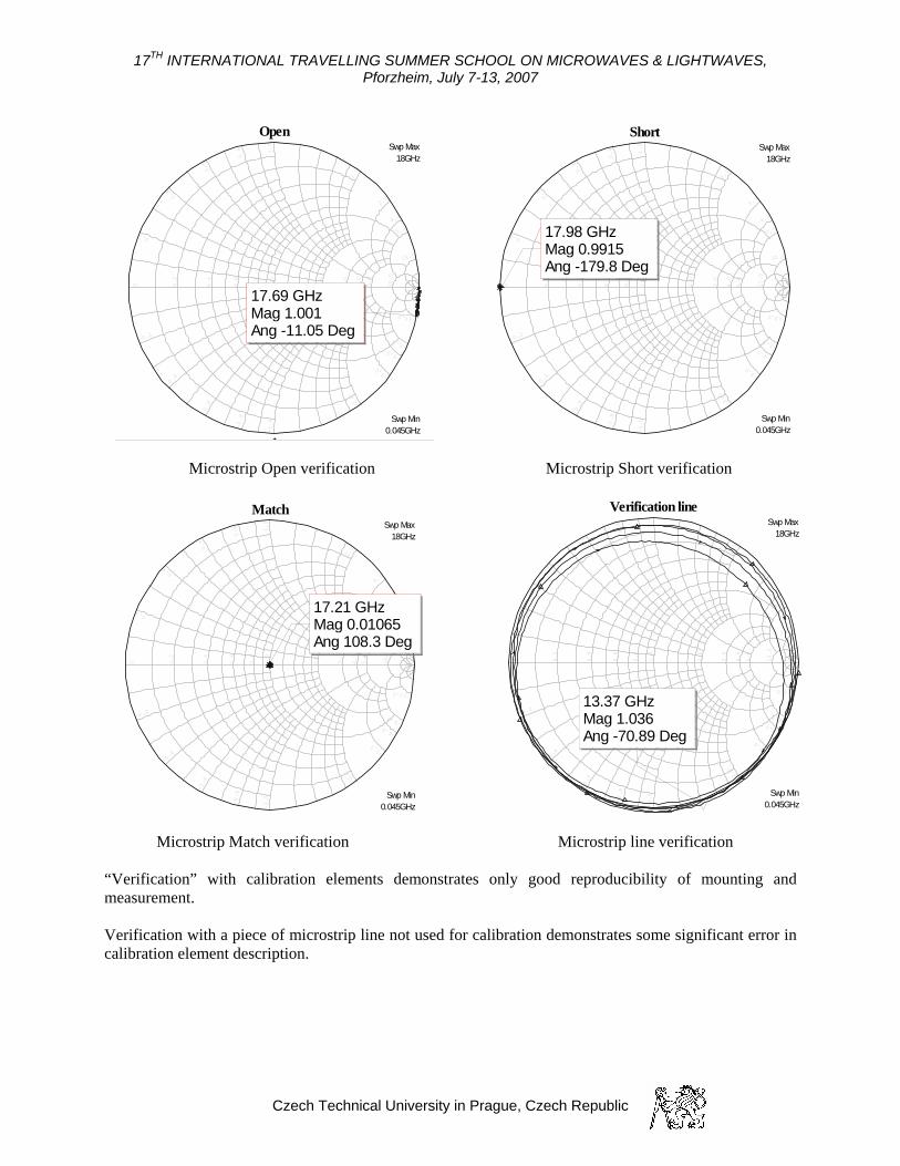
erification
Verification microstrip line
Microstrip Open Microstrip Short
Microstrip Match
V
Microstrip Open in the test fixture
Czech Technical University in Prague, Czech Republic
17TH INTERNATIONAL TRAVELLING SUMMER SCHOOL ON MICROWAVES & LIGHTWAVES, Pforzheim, July 7-13, 2007
Microstrip Open verification Microstrip Short verification
me
Microstrip Match verification Microstrip line verification
“Verification” with calibration elements demonstrates only good reproducibility of mounting and asurement.
Verification with a piece of microstrip line not used for calibration demonstrates some significant error in calibration element description.
0
1.0
10.0
10.0
-10.0
5.0
5.0
-5.0
0
3.
-3.0
4.0
4.0
-4.0
0.2
0.2
-0.2
0.4
-0.4
-0.
.8
1.0
2.0
3.0
0.4
0.6
0.8
-1.0-0
.
2.
0
-26
8
.0
0.6
0
OpenSwp Max
18GHz
Swp Min0.045GHz
17.69 GHzMag 1.001Ang -11.05 Deg
0 1.0
1.0
-1.0
10.0
10.0
-10.0
5.0
5.0
-5.0
2.0
2.0
-2.0
3.0
3.0
-3.0
4.0
4.0
-4.0
0.2
0.2
-0.2
0.4
-0.4
0.6
0.6
-0.6
0.8
0.8
-0.8
0.4
ShortSwp Max
18GHz
Swp Min0.045GHz
17.98 GHzMag 0.9915Ang -179.8 Deg
0 1.0
-1.0
10.0
10.0
-10.0
5.0
5.0
-5.0
2.0
2.0
-2.0
3.0
3.0
-3.0
4.0
4.0
-4.0
0.2
0.2
-0.2
0.4
0.4
-0.4
0.6
0.6
-0.6
0.8
-0.
1.0
0.8
8
MatchSw
0 1.0
1.0
-1.0
10.0
10.0
-10.0
5.0
5.0
-5.0
2.0
2.0
-2.0
3.0
3.0
-3.0
4.0
4.0
-4.0
0.2
0.2
-0.2
0.4
0.4
-0.4
0.6
0.6
0.8
0.8
-0
p Max18GHz
Swp Min0.045GHz
17.21 GHzMag 0.01065Ang 108.3 Deg
-0.6
.8
Verification lineSwp Max
18GHz
Swp Min0.045GHz
13.37 GHzMag 1.036Ang -70.89 Deg
Czech Technical University in Prague, Czech Republic
17TH INTERNATIONAL TRAVELLING SUMMER SCHOOL ON MICROWAVES & LIGHTWAVES, Pforzheim, July 7-13, 2007
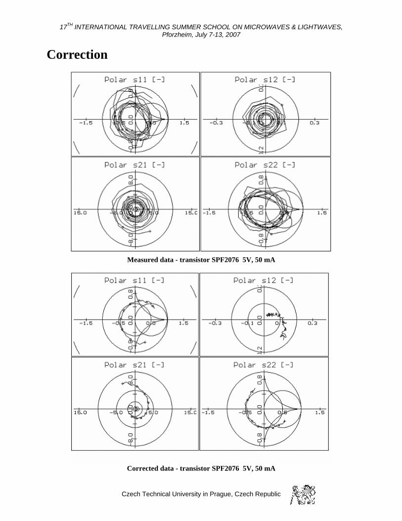
Correction
Measured data - transistor SPF2076 5V, 50 mA
Corrected data - transistor SPF2076 5V, 50 mA
Czech Technical University in Prague, Czech Republic
17TH INTERNATIONAL TRAVELLING SUMMER SCHOOL ON MICROWAVES & LIGHTWAVES, Pforzheim, July 7-13, 2007
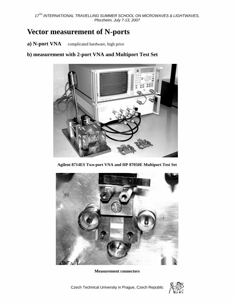
Vector measurement of N-ports a) N-port VNA complicated hardware, high price
b) measurement with 2-port VNA and Multiport Test Set
Measurement connectors
Agilent 8714ES Two-port VNA and HP 87050E Multiport Test Set
Czech Technical University in Prague, Czech Republic
17TH INTERNATIONAL TRAVELLING SUMMER SCHOOL ON MICROWAVES & LIGHTWAVES, Pforzheim, July 7-13, 2007
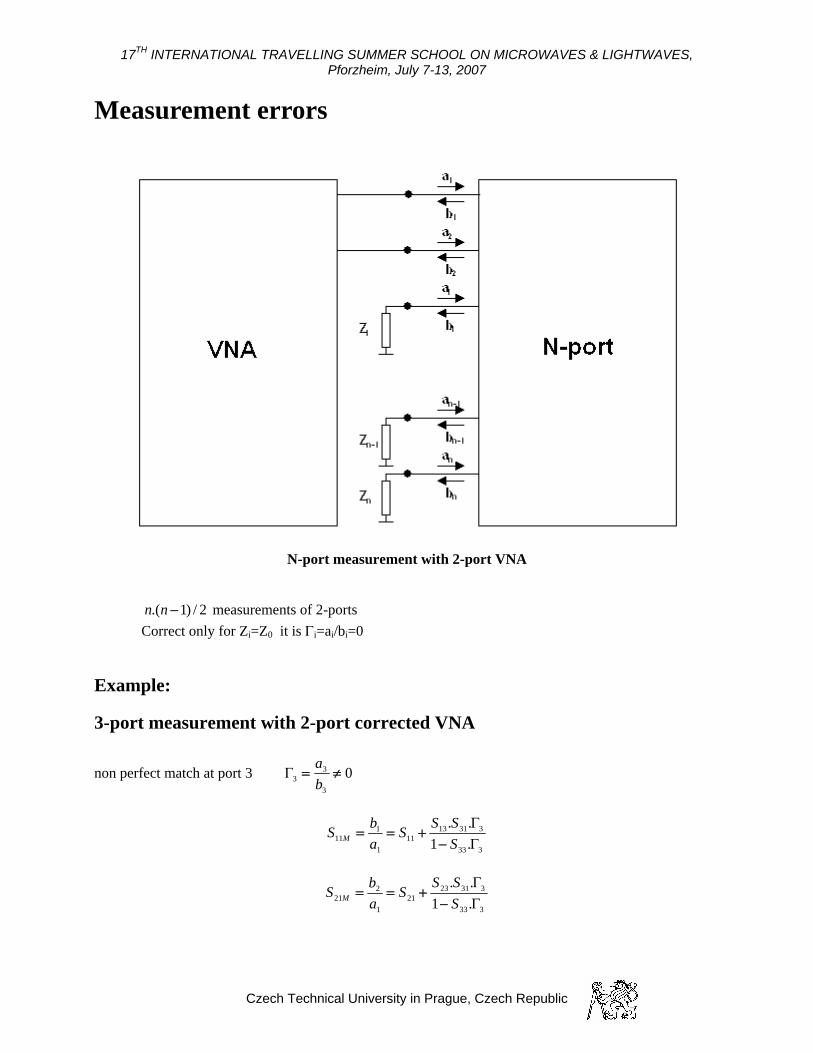
Measurement errors
measurements of 2-ports Correct only for Zi=Z0 it is Γi=ai/bi=0
Example:
non perfect ma
N-port measurement with 2-port VNA
2/)1.( −nn
3-port measurement with 2-port corrected VNA
tch at port 3 03
33 ≠=
ba
Γ
333
3311311
1
111 .1
..ΓΓ
SSSS
abS M −
+==
333
3312321
1
221 .1
..ΓΓ
SSS
SabS M −
+==
Czech Technical University in Prague, Czech Republic
17TH INTERNATIONAL TRAVELLING SUMMER SCHOOL ON MICROWAVES & LIGHTWAVES, Pforzheim, July 7-13, 2007
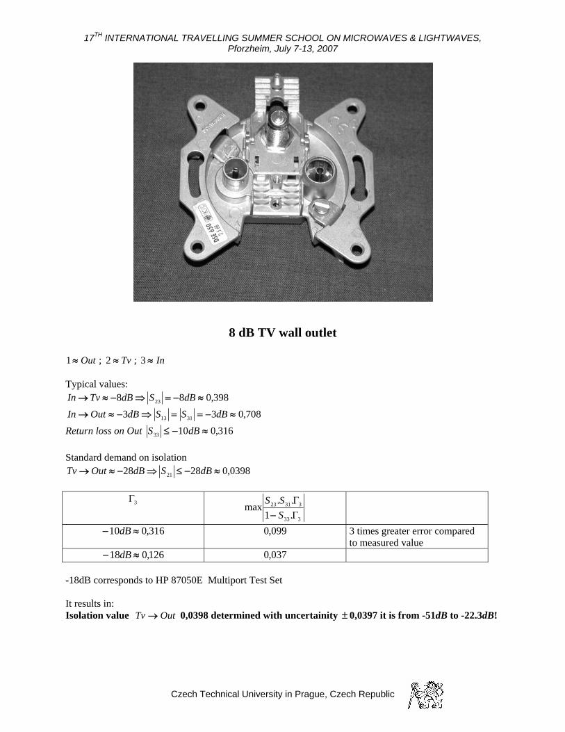
8 dB TV wall outlet
Out≈1 ; Tv≈2 ; In≈3 Typical values:
398,088 ≈−=⇒−≈→ dBSdBTvIn 23
708,033 3113
Return loss on Out ≈−==⇒−≈→ dBSSdBOutIn
316,01033 ≈−≤ dBS Standard demand on isolation
0398,02828 21 ≈−≤⇒−≈→ dBSdBOutTv
3Γ
333
33123
.1..maxΓΓ
SSS
−
316,010 ≈− dB 099,0 3 times greater error compared to measured value
126,018 ≈− dB 037,0 -18dB corresponds to HP 87050E Multiport Test Set It results in: Isolation value 0,0398 determined with uncertainity OutTv → ± 0,0397 it is from -51dB to -22.3dB!
Czech Technical University in Prague, Czech Republic
17TH INTERNATIONAL TRAVELLING SUMMER SCHOOL ON MICROWAVES & LIGHTWAVES, Pforzheim, July 7-13, 2007
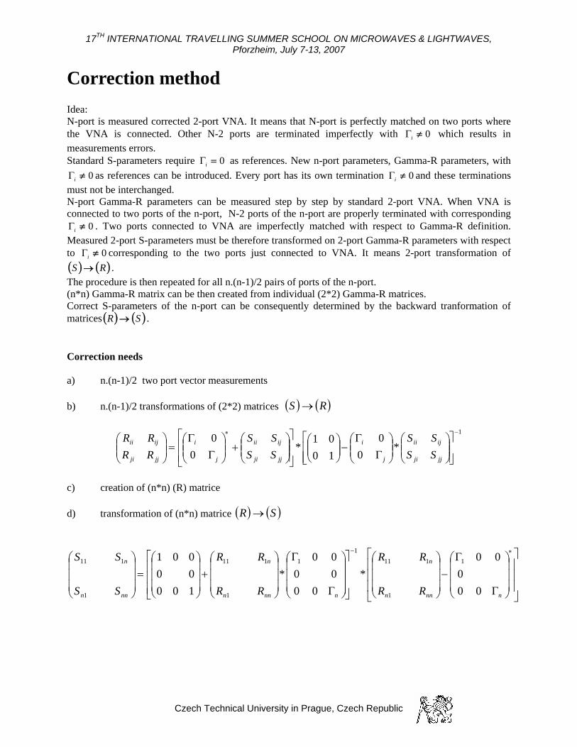
Correctio Idea: N-port is me s perfectly matched on two ports where the VNA is connected. Other N-2 ports are ter inated imperfectly with which results in measurements errors. Standard S-parameters require as references. -port parameters, Gamma-R parameters, with
as references can be introduced. Every port has its own termination
n method
that N-port iasured corrected 2-port VNA. It meansm 0≠iΓ
New n0=iΓ0≠iΓ 0≠iΓ and these terminations
ust not be interchanged. -port Gamma-R parameters can be measured step by step by standard 2-port VNA. When VNA is
onnected to two ports of the n-port, N-2 ports of the n-port are properly terminated with corresponding . Two ports connected to VNA are imperfectly matched with respect to Gamma-R definition.
easured 2-port S-parameters must be therefore transformed on 2-port Gamma-R parameters with respect corresponding to the two ports just connected to VNA. It means 2-port transformation of
. he procedure is then repeated for all n.(n-1)/2 pairs of ports of the n-port. *n) Gamma-R matrix can be then created from individual (2*2) Gamma-R matrices. orrect S-parameters of the n-port can be consequently determined by the backward tranformation of atrice
Correction needs
ments
b) n.(n-1)/2 transformations of (2*2) matrices
mNc
0≠iΓMto 0≠iΓ( ) ( )RS →T(nC
s ( ) ( )SR → . m
a) n.(n-1)/2 two port vector measure
( ) ( )RS →
c) creation of (n*n) (R) matrice d) transformation of (n*n) matrice
1
*0
01001
*0
0−∗
⎥⎥⎦
⎤
⎢⎢⎣
⎡⎟⎟⎠
⎞⎜⎜⎝
⎛⎟⎟⎠
⎞⎜⎜⎝
⎛Γ
Γ−⎟⎟
⎠
⎞⎜⎜⎝
⎛
⎥⎥⎦
⎤
⎢⎢⎣
⎡⎟⎟⎠
⎞⎜⎜⎝
⎛+⎟⎟
⎠
⎞⎜⎜⎝
⎛Γ
Γ=⎟⎟
⎠
⎞⎜⎜⎝
⎛
jjji
ijii
j
i
jjji
ijii
j
i
jjji
ijii
SSSS
SSSS
RRRR
( ) ( )SR →
⎥⎥⎥
⎦
⎤
⎢⎢⎢
⎣
⎡
⎟⎟⎟
⎠
⎞
⎜⎜⎜
⎝
⎛
Γ
Γ−
⎟⎟⎟
⎠
⎞
⎜⎜⎜
⎝
⎛
⎥⎥⎥
⎦
⎤
⎢⎢⎢
⎣
⎡
⎟⎟⎟
⎠
⎞
⎜⎜⎜
⎝
⎛
Γ
Γ
⎟⎟⎟
⎠
⎞
⎜⎜⎜
⎝
⎛+
⎟⎟⎟
⎠
⎞
⎜⎜⎜
⎝
⎛=
⎟⎟⎟
⎠
⎞
⎜⎜⎜
⎝
⎛∗−
nnnn
n
nnnn
n
nnn
n
RR
RR
RR
RR
SS
SS
000
00*
000000
*10000001 1
1
1111
1
1
111
1
111
Czech Technical University in Prague, Czech Republic
17TH INTERNATIONAL TRAVELLING SUMMER SCHOOL ON MICROWAVES & LIGHTWAVES, Pforzheim, July 7-13, 2007
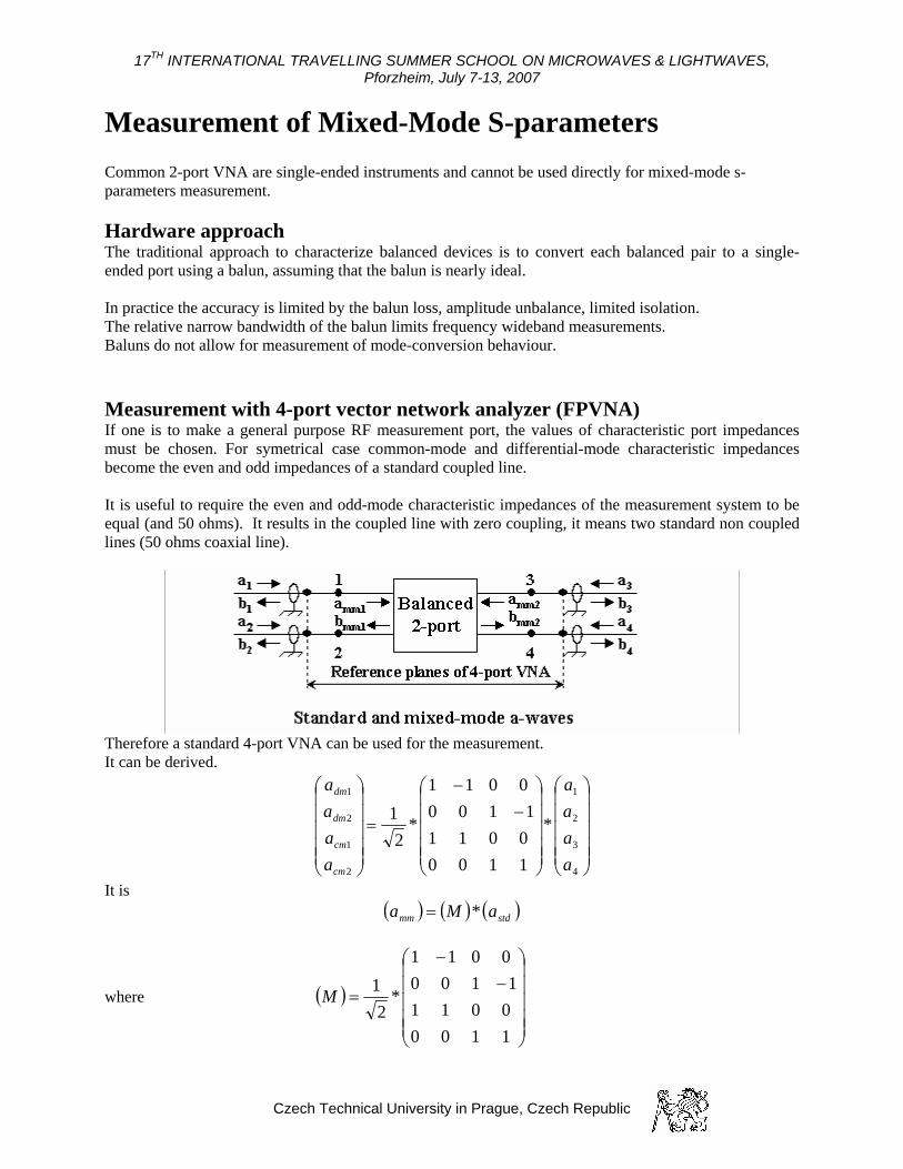
Measurement of Mixed-Mode S-parameters Common 2-port VNA are single-ended instruments and cannot be used directly for mixed-mode s-parameters measurement. Hardware approach The traditional approach to characterize balanced devices is to convert each balanced pair to a single-ended port using a balun, assuming that the balun is nearly ideal. In practice the accuracy is limited by the balun loss, amplitude unbalance, limited isolation. The relative narrow bandwidth of the balun limits frequency wideband measurements. Baluns do not allow for measurement of mode-conversion behaviour. Measurement with 4-port vector network analyzer (FPVNA) If one is to make a general purpose RF measurement port, the values of characteristic port impedances must be chosen. For symetrical case common-mode and differential-mode characteristic impedances become the even and odd impedances of a standard coupled line. It is useful to require the even and odd-mode characteristic impedances of the measurement system to be equal (and 50 ohms). It results in the coupled line with zero coupling, it means two standard non coupled
nes (50 ohms coaxial line).
t.
li
Therefore a standard 4-port VNA can be used for the measuremenIt can be derived.
⎟⎟⎟⎟⎟
⎠
⎞
⎜⎜⎜⎜⎜
⎝
⎛
⎟⎟⎟⎟⎟
⎠
⎞
⎜⎜⎜⎜⎜
⎝
⎛−
−
=
⎟⎟⎟⎟⎟
⎠
⎞
⎜⎜⎜⎜⎜
⎝
⎛
4
3
2
1
2
1
2
1
*
110000111100
0011
*2
1
aaaa
aaaa
cm
cm
dm
dm
It is ( ) ( ) ( )stdmm aMa *=
where ( )⎟⎟⎟⎟⎟
⎠
⎞
⎜⎜⎜⎜⎜
⎝
⎛−
−
=
110000111100
0011
*2
1M
Czech Technical University in Prague, Czech Republic
17TH INTERNATIONAL TRAVELLING SUMMER SCHOOL ON MICROWAVES & LIGHTWAVES, Pforzheim, July 7-13, 2007
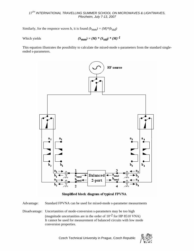
Similarly, for the responce waves b, it is found (bmm) = (M)*(bstd) Which yields (Smm) = (M) * (Sstd) * (M)-1 This equation illustrates the possibility to calculate the mixed-mode s-parameters from the standard single-ended s-parameters.
dvantage: Standard FPVNA can be used for mixed-mode s-parameter measurments
b (magnitude uncertanities are in the order of 10-2 for HP 8510 VNA) It cannot be used for measurement of balanced circuits with low mode conversion properties.
A Disadvantage: Uncertanities of mode-conversion s-parameters may e too high
Czech Technical University in Prague, Czech Republic
17TH INTERNATIONAL TRAVELLING SUMMER SCHOOL ON MICROWAVES & LIGHTWAVES, Pforzheim, July 7-13, 2007
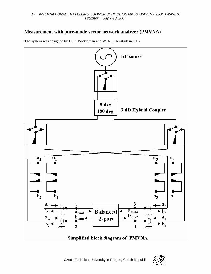
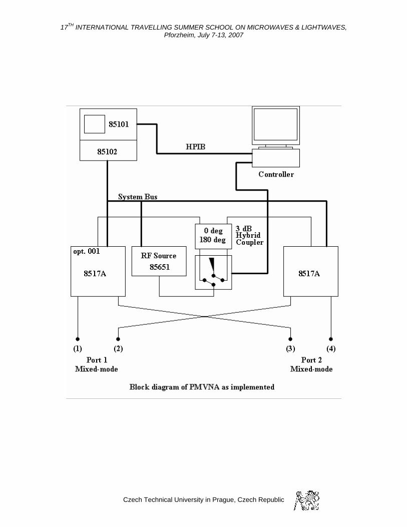
Measurement with pure-mode vector network analyzer (PMVNA)
stem was designed by D. E. Bockleman and W. R. Eisenstadt in 1997. The sy
Czech Technical University in Prague, Czech Republic
17TH INTERNATIONAL TRAVELLING SUMMER SCHOOL ON MICROWAVES & LIGHTWAVES, Pforzheim, July 7-13, 2007
Czech Technical University in Prague, Czech Republic
17TH INTERNATIONAL TRAVELLING SUMMER SCHOOL ON MICROWAVES & LIGHTWAVES, Pforzheim, July 7-13, 2007
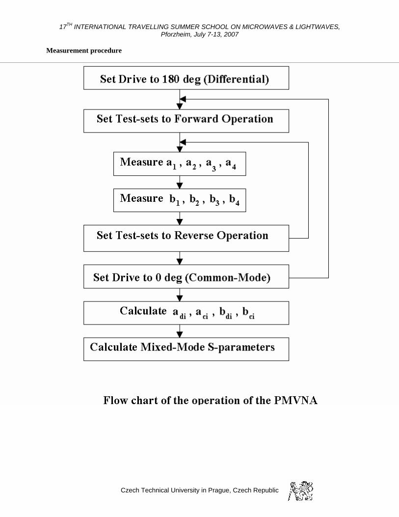
Measurement procedure
Czech Technical University in Prague, Czech Republic
17TH INTERNATIONAL TRAVELLING SUMMER SCHOOL ON MICROWAVES & LIGHTWAVES, Pforzheim, July 7-13, 2007
Advantage: Uncertanities of mode-conversion s-parameters are low (magnitude uncertanities are in the order of 10-4 for HP 8510 VNA) Disadvantage: More complicated system Comparison of PMVNA and FPVNA: PMVNA has about equal magnitude error as FPVNA when pure mode Sdd and Scc s-parameters of a differential device are measured. PMVNA can have substantially lower error compared to FPVNA when mixed-mode Sdc and Scd s-parameters of a differential device are measured. FPVNA has lower uncertanities when measuring a device that naturally operates with ground referenced modes
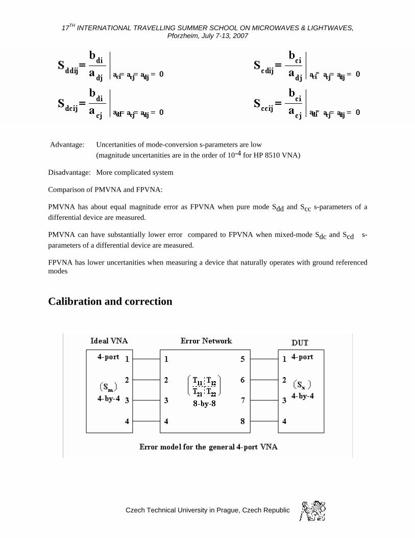
Calibration and correction
Czech Technical University in Prague, Czech Republic
17TH INTERNATIONAL TRAVELLING SUMMER SCHOOL ON MICROWAVES & LIGHTWAVES, Pforzheim, July 7-13, 2007
The error model includes all possible error terms, including all port-to-port leakage paths. There are x8=64 error terms including 4x4(4-1)=48 leakage terms.
ossible simplification neglecting all leakage between ports (crosstalks) gives no-leakage model, leaving total of 4x4=16 error rms
The relationship between measured s-parameters (Sm ) and actual s-parameters (Sa) is given by: (T11 )(Sa) + (T12) + (Sm)(T21)(Sa) - (Sm)(T22) = (0) where (Tij) are submatrices of cascadable (chainable) t-parameters. It can be shown that at least five 4-port calibration standards is necessary to determine unknown sub-matrices Tij in the case of the full error model. (Each standard generates 16 equations). At least two transmission standards are necessary for the no-leakage error model. The corrected s-parameters of the DUT are then determined by: (Sx) = [(T22)(Sm) - (T12)].[-(T21)(Sm) + T11]-1
Conclusion 40 years old history of microwave wideband vector measurement Still increasing applications of vector measurement
8 P- te
Czech Technical University in Prague, Czech Republic
17TH INTERNATIONAL TRAVELLING SUMMER SCHOOL ON MICROWAVES & LIGHTWAVES, Pforzheim, July 7-13, 2007
References D. E. Bockleman and W. R. Eisenstadt, "Combined differential and common-mode scattering parameters: Theory and simulation." IEEE Trans. Microwave Theory Tech., vol. 43, pp. 1530-1539, July 1995 D. E. Bockleman and W. R. Eisenstadt, "Pure-Mode Network Analyzer for On-Wafer Measurements of Mixed-Mode S-parameters of Differential Circuits," IEEE Trans. Microwave Theory Tech., vol. 45, No. 7, pp. 1071-1077, July 1997 D. E. Bockleman and W. R. Eisenstadt, "Calibration and Verification of the Pure-Mode Vector Network Analyzer," IEEE Trans. Microwave Theory Tech., vol. 46, No. 7, pp. 1009-1012, July 1998 D. E. Bockleman and W. R. Eisenstadt, "Accuracy Estimation of Mixed-Mode Scattering Parameter Measurements,"IEEE Trans. Microwave Theory Tech., vol. 47, No. 1, pp. 102-105, January 1999 Vahe Adamian, B. Cole, "VNA-Based System Tests Differential Components," Microwaves and RF, March 2000, pp. 126-162 R. A. Speciale, "A Generalization of the TSD Network-Analyzer Calibration Procedure, Covering n-Port Scattering-Parameters Measurements, Affected by Leakage Errors," IEEE Trans. Microwave Theory Tech., vol. 25, No. 12, pp. 1100-1115, December 1977 J. V. Butler, D. K. Rytting, M. F. Iskander, R. D. Pollard, and M. V. Bossche, "16-term Error Model and Calibration Procedure for On-Wafer Network Analysis Measurements," IEEE Trans. Microwave Theory Tech., vol. 39, No. 12, pp. 22112217, December 1991 G. F. Engen, "Calibration the Six-Port Reflectometer by Means of Sliding Terminations," IEEE Trans. Microwave Theory Tech., vol. 26, No. 12, pp. 951-957, December 1978 K. Hoffmann and Z. Skvor, "A Novel Vector Network Analyzer," IEEE Trans. Microwave Theory Tech., vol. 46, No. 12, pp. 2520-2523, December 1998 Rautio J. C., "Techniques for Correcting Scaterring Parameters Data of an Imperfectly Terminated Multiport when Measured with a Two Port Network Analyzer", IEEE Trans. on MTT, vol. MTT-31, No.5, May 1983, pp. 407-412
Czech Technical University in Prague, Czech Republic