Embed Size (px)
Citation preview

µA723PRECISION VOLTAGE REGULATORS
SLVS057D – AUGUST 1972 – REVISED JULY 1999
1POST OFFICE BOX 655303 • DALLAS, TEXAS 75265
150-mA Load Current Without ExternalPower Transistor
Adjustable Current-Limiting Capability
Input Voltages up to 40 V
Output Adjustable From 2 V to 37 V
Direct Replacement for Fairchild µA723C
description
The µA723 is a precision integrated-circuitvoltage regulator, featuring high ripple rejection,excellent input and load regulation, excellent temperature stability, and low standby current. The circuit consistsof a temperature-compensated reference-voltage amplifier, an error amplifier, a 150-mA output transistor, andan adjustable-output current limiter.
The µA723 is designed for use in positive or negative power supplies as a series, shunt, switching, or floatingregulator. For output currents exceeding 150 mA, additional pass elements can be connected as shown inFigures 4 and 5.
The µA723C is characterized for operation from 0°C to 70°C.
AVAILABLE OPTIONS
PACKAGED DEVICESCHIP
TAPLASTIC
DIP(N)
SMALLOUTLINE
(D)
CHIPFORM
(Y)
0°C to 70°C µA723CN µA723CD µA723Y
The D package is available taped and reeled. Add the suffixR to the device type (e.g., µA723CDR). Chip forms aretested at 25°C.
functional block diagram
–
+
VCC– CURR LIM CURR SENS VZ
CurrentLimiter
VCSeries PassTransistor
RegulatedOutput
VCC+
RefAmp
CurrentSource
Temperature-Compensated
Reference Diode
FREQ COMP
REF
IN–
IN+
ErrorAmp
Please be aware that an important notice concerning availability, standard warranty, and use in critical applications ofTexas Instruments semiconductor products and disclaimers thereto appears at the end of this data sheet.
Copyright 1999, Texas Instruments IncorporatedPRODUCTION DATA information is current as of publication date.Products conform to specifications per the terms of Texas Instrumentsstandard warranty. Production processing does not necessarily includetesting of all parameters.
1
2
3
4
5
6
7
14
13
12
11
10
9
8
NCCURR LIM
CURR SENSIN–IN+
REFVCC–
NCFREQ COMPVCC+VCOUTPUTVZNC
D OR N PACKAGE(TOP VIEW)

µA723PRECISION VOLTAGE REGULATORS
SLVS057D – AUGUST 1972 – REVISED JULY 1999
2 POST OFFICE BOX 655303 • DALLAS, TEXAS 75265
schematic
VCC+ VC
15 kΩ OUTPUT
6.2 V
VZ
FREQ COMP
CURR SENS
CURR LIM
IN–IN+REF
150 Ω
1 kΩ
20 kΩ300 Ω5 kΩ
30 kΩ
100 Ω
1 kΩ25 kΩ500 Ω
15 kΩ
5 pF
VCC–
Resistor and capacitor values shown are nominal.
absolute maximum ratings over operating free-air temperature range (unless otherwise noted) †
Peak voltage from VCC+ to VCC– (tw ≤ 50 ms) 50 V. . . . . . . . . . . . . . . . . . . . . . . . . . . . . . . . . . . . . . . . . . . . . . . . . Continuous voltage from VCC+ to VCC– 40 V. . . . . . . . . . . . . . . . . . . . . . . . . . . . . . . . . . . . . . . . . . . . . . . . . . . . . . . Input-to-output voltage differential 40 V. . . . . . . . . . . . . . . . . . . . . . . . . . . . . . . . . . . . . . . . . . . . . . . . . . . . . . . . . . . . Differential input voltage to error amplifier ±5 V. . . . . . . . . . . . . . . . . . . . . . . . . . . . . . . . . . . . . . . . . . . . . . . . . . . . . Voltage between noninverting input and VCC– 8 V. . . . . . . . . . . . . . . . . . . . . . . . . . . . . . . . . . . . . . . . . . . . . . . . . . Current from VZ 25 mA. . . . . . . . . . . . . . . . . . . . . . . . . . . . . . . . . . . . . . . . . . . . . . . . . . . . . . . . . . . . . . . . . . . . . . . . . Current from REF 15 mA. . . . . . . . . . . . . . . . . . . . . . . . . . . . . . . . . . . . . . . . . . . . . . . . . . . . . . . . . . . . . . . . . . . . . . . . Package thermal impedance, θJA (see Notes 1 and 2): D package 86°C/W. . . . . . . . . . . . . . . . . . . . . . . . . . . .
N package 101°C/W. . . . . . . . . . . . . . . . . . . . . . . . . . . Lead temperature 1,6 mm (1/16 inch) from case for 10 seconds: D or N package 260°C. . . . . . . . . . . . . . . . Storage temperature range, Tstg –65°C to 150°C. . . . . . . . . . . . . . . . . . . . . . . . . . . . . . . . . . . . . . . . . . . . . . . . . . .
† Stresses beyond those listed under “absolute maximum ratings” may cause permanent damage to the device. These are stress ratings only, andfunctional operation of the device at these or any other conditions beyond those indicated under “recommended operating conditions” is notimplied. Exposure to absolute-maximum-rated conditions for extended periods may affect device reliability.
NOTES: 1. Maximum power dissipation is a function of TJ(max), θJA, and TA. The maximum allowable power dissipation at any allowableambient temperature is PD = (TJ(max) – TA)/θJA. Operating at the absolute maximum TJ of 150°C can impact reliability.
2. The package thermal impedance is calculated in accordance with JESD 51, except for through-hole packages, which use a tracelength of zero.

µA723PRECISION VOLTAGE REGULATORS
SLVS057D – AUGUST 1972 – REVISED JULY 1999
3POST OFFICE BOX 655303 • DALLAS, TEXAS 75265
recommended operating conditions
MIN MAX UNIT
Input voltage, VI 9.5 40 V
Output voltage, VO 2 37 V
Input-to-output voltage differential, VC – VO 3 38 V
Output current, IO 150 mA
Operating free-air temperature range, TA µA723C 0 70 °C
electrical characteristics at specified free-air temperature (see Notes 3 and 4)
PARAMETER TEST CONDITIONS TµA723C
UNITPARAMETER TEST CONDITIONS TA MIN TYP MAXUNIT
VI = 12 V to VI = 15 V 25°C 0.1 1
Input regulation VI = 12 V to VI = 40 V 25°C 1 5 mV/V
VI = 12 V to VI = 15 V 0°C to 70°C 3
Ripple rejectionf = 50 Hz to 10 kHz, Cref = 0 25°C 74
dBRipple rejectionf = 50 Hz to 10 kHz, Cref = 5 µF 25°C 86
dB
Output regulation25°C –0.3 –2
mV/VOutput regulation0°C to 70°C –6
mV/V
Reference voltage, Vref 25°C 6.8 7.15 7.5 V
Standby current VI = 30 V, IO = 0 25°C 2.3 4 mA
Temperature coefficient of output voltage 0°C to 70°C 0.003 0.015 %/°C
Short-circuit output current RSC = 10 Ω, VO = 0 25°C 65 mA
Output noise voltageBW = 100 Hz to 10 kHz, Cref = 0 25°C 20
µVOutput noise voltageBW = 100 Hz to 10 kHz, Cref = 5 µF 25°C 2.5
µV
NOTES: 3. For all values in this table, the device is connected as shown in Figure 1 with the divider resistance as seen by the error amplifier≤ 10 kΩ. Unless otherwise specified, VI = VCC+ = VC = 12 V, VCC– = 0, VO = 5 V, IO = 1 mA, RSC = 0, and Cref = 0.
4. Pulse-testing techniques must be used that will maintain the junction temperature as close to the ambient temperature as possible.
electrical characteristics, T A = 25°C (see Notes 3 and 4)
PARAMETER TEST CONDITIONSµA723Y
UNITPARAMETER TEST CONDITIONSMIN TYP MAX
UNIT
Input regulationVI = 12 V to VI = 15 V 0.1
mV/VInput regulationVI = 12 V to VI = 40 V 1
mV/V
Ripple rejectionf = 50 Hz to 10 kHz, Cref = 0 74
dBRipple rejectionf = 50 Hz to 10 kHz, Cref = 5 µF 86
dB
Output regulation –0.3 mV/V
Reference voltage, Vref 7.15 V
Standby current VI = 30 V, IO = 0 2.3 mA
Short-circuit output current RSC = 10 Ω, VO = 0 65 mA
Output noise voltageBW = 100 Hz to 10 kHz, Cref = 0 20
µVOutput noise voltageBW = 100 Hz to 10 kHz, Cref = 5 µF 2.5
µV
NOTES: 3. For all values in this table, the device is connected as shown in Figure 1 with the divider resistance as seen by the error amplifier≤ 10 kΩ. Unless otherwise specified, VI = VCC+ = VC = 12 V, VCC– = 0, VO = 5 V, IO = 1 mA, RSC = 0, and Cref = 0.
4. Pulse-testing techniques must be used that will maintain the junction temperature as close to the ambient temperature as possible.

µA723PRECISION VOLTAGE REGULATORS
SLVS057D – AUGUST 1972 – REVISED JULY 1999
4 POST OFFICE BOX 655303 • DALLAS, TEXAS 75265
APPLICATION INFORMATION
Table 1. Resistor Values (k Ω) for Standard Output Voltages
OUTPUTVOLTAGE
APPLICABLEFIGURES
FIXED OUTPUT±5%
OUTPUT ADJUSTABLE±10%
(SEE NOTE 6)
(V) (SEE NOTE 5) R1(kΩ)
R2(kΩ)
R1(kΩ)
P1(kΩ )
P2(kΩ )
3.0 1, 5, 6, 9, 11, 12 (4) 4.12 3.01 1.8 0.5 1.2
3.6 1, 5, 6, 9, 11, 12 (4) 3.57 3.65 1.5 0.5 1.5
5.0 1, 5, 6, 9, 11, 12 (4) 2.15 4.99 0.75 0.5 2.2
6.0 1, 5, 6, 9, 11, 12 (4) 1.15 6.04 0.5 0.5 2.7
9.0 2, 4, (5, 6, 9, 12) 1.87 7.15 0.75 1.0 2.7
12 2, 4, (5, 6, 9, 12) 4.87 7.15 2.0 1.0 3.0
15 2, 4, (5, 6, 9, 12) 7.87 7.15 3.3 1.0 3.0
28 2, 4, (5, 6, 9, 12) 21.0 7.15 5.6 1.0 2.0
45 7 3.57 48.7 2.2 10 39
75 7 3.57 78.7 2.2 10 68
100 7 3.57 105 2.2 10 91
250 7 3.57 255 2.2 10 240
–6(see Note 7)
3, 10 3.57 2.43 1.2 0.5 0.75
–9 3, 10 3.48 5.36 1.2 0.5 2.0
–12 3, 10 3.57 8.45 1.2 0.5 3.3
–15 3, 10 3.57 11.5 1.2 0.5 4.3
–28 3, 10 3.57 24.3 1.2 0.5 10
–45 8 3.57 41.2 2.2 10 33
–100 8 3.57 95.3 2.2 10 91
–250 8 3.57 249 2.2 10 240
NOTES: 5. The R1/R2 divider can be across either VO or V(ref). If the divider is acrossV(ref), use the figure numbers without parentheses. If the divider is acrossVO, use the figure numbers in parentheses.
6. To make the voltage adjustable, the R1/R2 divider shown in the figures mustbe replaced by the divider shown below.
R1
P1
R2
Adjustable Output Circuit
7. For Figures 3, 8, and 10, the device requires a minimum of 9 V between VCC+and VCC– when VO is equal to or more positive than –9 V.

µA723PRECISION VOLTAGE REGULATORS
SLVS057D – AUGUST 1972 – REVISED JULY 1999
5POST OFFICE BOX 655303 • DALLAS, TEXAS 75265
APPLICATION INFORMATION
Table 2. Formulas for Intermediate Output Voltages
OUTPUTS FROM 2 V TO 7 VSEE FIGURES 1, 5, 6, 9, 11, 12 (4)
AND NOTE 5
OUTPUTS FROM 4 V TO 250 VSEE FIGURE 7 AND NOTE 5 CURRENT LIMITING
VO V(ref) R2
R1R2VO
V(ref)
2
R2 – R1R1
R3 R4
I(limit)0.65 V
RSC
OUTPUTS FROM 7 V TO 37 VSEE FIGURES 2, 4, (5, 6, 9, 11, 12)
AND NOTE 5
OUTPUTS FROM –6 V TO –250 VSEE FIGURES 3, 8, 10AND NOTES 5 AND 7
FOLDBACK CURRENT LIMITINGSEE FIGURE 6
VO V(ref) R1R2
R2
VO –V(ref)
2
R1R2R1
R3 R4
I(knee)VOR3 (R3R4) 0.65 V
RSCR4
IOS0.65 V
RSC
R3R4R4
NOTES: 5. The R1/R2 divider can be across either VO or V(ref). If the divider is across V(ref), use figure numbers without parentheses. If thedivider is across VO, use the figure numbers in parentheses.
7. For Figures 3, 8, and 10, the device requires a minimum of 9 V between VCC+ and VCC– when VO is equal to or more positive than–9 V.
REF
VI
VCC+ VC
OUTPUT
VZCURR LIM
CURR SENS
IN+
VCC– FREQ COMPIN–
RSCR1
C(ref)
R2 100 pF
RegulatedOutput, V O
R3 (see Notes A and B)
µA723
NOTES: A.
B. R3 can be eliminated for minimum component count. Use direct connection (i.e., R3 = 0).
R3 R1R2R1R2
for a minimum VO
Figure 1. Basic Low-Voltage Regulator (V O = 2 V to 7 V)

µA723PRECISION VOLTAGE REGULATORS
SLVS057D – AUGUST 1972 – REVISED JULY 1999
6 POST OFFICE BOX 655303 • DALLAS, TEXAS 75265
APPLICATION INFORMATION
100 pF R2
R1
Regulated Output,VO
RSC
VI
REF
VCC+ VC
OUTPUT
VZCURR LIM
CURR SENS
IN+
VCC– FREQ COMPIN–
R3(see Notes A and B)
µA723
NOTES: A.
B. R3 can be eliminated for minimum component count. Use direct connection (i.e., R3 = 0).
R3 R1R2R1R2
for a minimum VO
Figure 2. Basic High-Voltage Regulator (V O = 7 V to 37 V)
R2
VI
100 pF
2N5001
2 kΩ
R3 =3 kΩ
R4 = 3 kΩ
R1
REF
VCC+ VCOUTPUT
VZCURR LIM
CURR SENS
IN+VCC– FREQ COMP
IN–
µA723
Regulated Output,VO
Figure 3. Negative-Voltage Regulator
µA723PRECISION VOLTAGE REGULATORS
SLVS057D – AUGUST 1972 – REVISED JULY 1999
7POST OFFICE BOX 655303 • DALLAS, TEXAS 75265
APPLICATION INFORMATION
VI
500 pF
R2
R1
RSC
2N3997REF
VCC+ VC
OUTPUT
VZCURR LIM
CURR SENS
IN+
VCC– FREQ COMPIN–
µA723
Regulated Output,VO
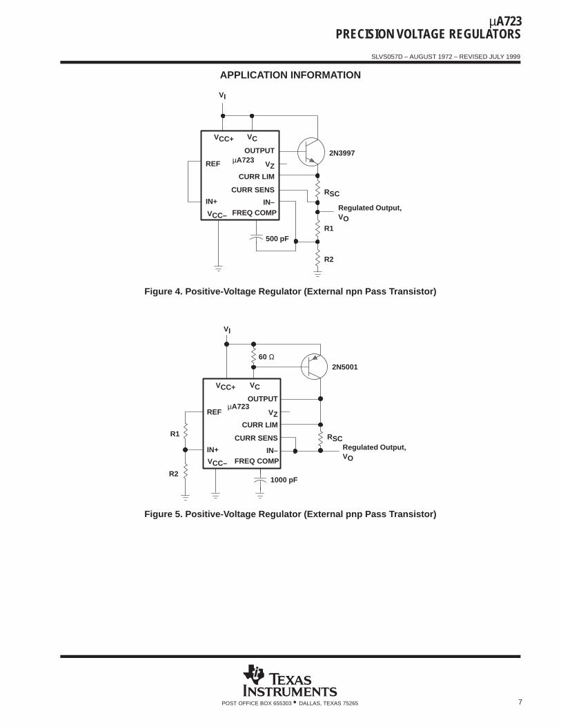
Figure 4. Positive-Voltage Regulator (External npn Pass Transistor)
RSCR1
R2
2N5001
VI
60 Ω
REF
VCC+ VC
OUTPUT
VZCURR LIM
CURR SENS
IN+
VCC– FREQ COMPIN–
µA723
1000 pF
Regulated Output,VO
Figure 5. Positive-Voltage Regulator (External pnp Pass Transistor)
µA723PRECISION VOLTAGE REGULATORS
SLVS057D – AUGUST 1972 – REVISED JULY 1999
8 POST OFFICE BOX 655303 • DALLAS, TEXAS 75265
APPLICATION INFORMATION
1000 pFR2
R1
VI
RSC
R3
R4 VO
IOS
lkneeIO
REF
VCC+ VC
OUTPUT
VZCURR LIM
CURR SENS
IN+
VCC– FREQ COMPIN–
µA723
Regulated Output,VO
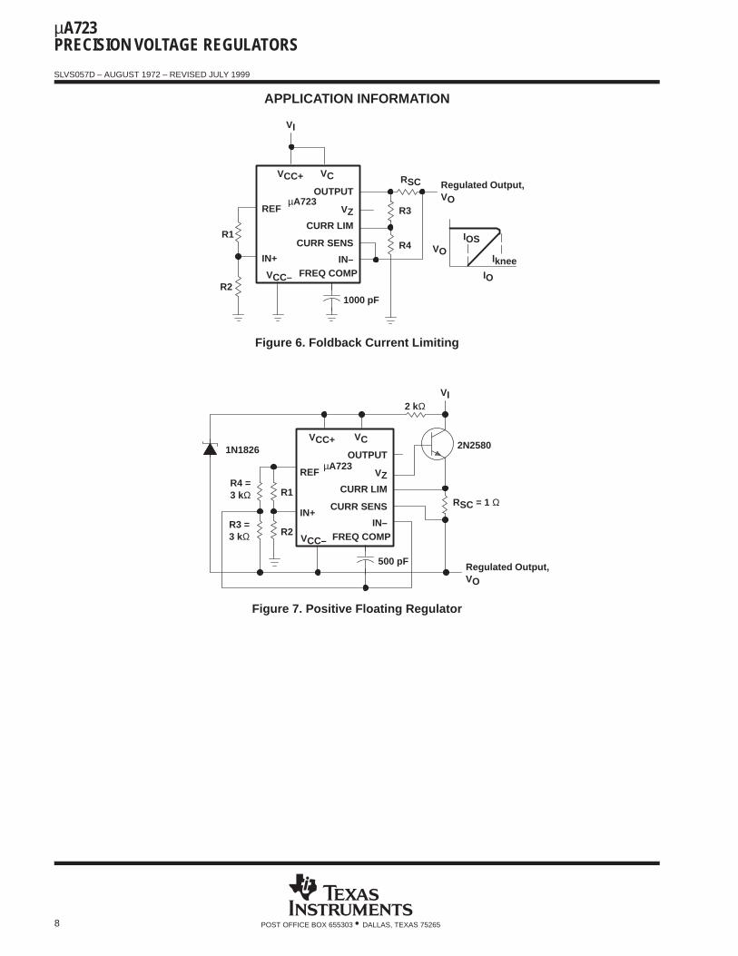
Figure 6. Foldback Current Limiting
R1
R2
2N2580
VI
RSC = 1 Ω
2 kΩ
500 pF
1N1826
REF
VCC+ VC
OUTPUT
VZCURR LIM
CURR SENSIN+
VCC– FREQ COMPIN–
µA723
R4 =3 kΩ
R3 =3 kΩ
Regulated Output,VO
Figure 7. Positive Floating Regulator

µA723PRECISION VOLTAGE REGULATORS
SLVS057D – AUGUST 1972 – REVISED JULY 1999
9POST OFFICE BOX 655303 • DALLAS, TEXAS 75265
APPLICATION INFORMATION
2N5287
10 kΩ
1N759
R2
R1
500 pF
10 kΩ
VI
REF
VCC+ VC
OUTPUT
VZCURR LIM
CURR SENS
IN+
VCC– FREQ COMPIN–
µA723
Regulated Output,VO
R3 =3 kΩ
R4 =3 kΩ
Figure 8. Negative Floating Regulator
0.1 µF
R1
R2
1 kΩ
1 MΩ1N4005
L = 1.2 mH(see Note A)
2N5005
2N51533 kΩ
VI
51 ΩREF
VCC+ VC
OUTPUT
VZCURR LIM
CURR SENS
IN+
VCC– FREQ COMP
IN–
µA723
NOTE A: L is 40 turns of No. 20 enameled copper wire wound on Ferroxcube P36/22-3B7 potted core, or equivalent, with a 0.009-inch air gap.
Regulated Output,VO
Figure 9. Positive Switching Regulator

µA723PRECISION VOLTAGE REGULATORS
SLVS057D – AUGUST 1972 – REVISED JULY 1999
10 POST OFFICE BOX 655303 • DALLAS, TEXAS 75265
APPLICATION INFORMATION
R2
VI
15 pF
2N5004
1 kΩ
(see Note A)
R1
2N3997
1N4005
1 MΩ
100 µF
1 kΩ
220 Ω
0.1 µF
L = 1.2 mH(see Note B)
REF
VCC+ VC
OUTPUT
VZCURR LIM
CURR SENSIN+
VCC– FREQ COMPIN–
µA723
NOTES: A. The device requires a minimum of 9 V between VCC+ and VCC– when VO is equal to or more positive than –9 V.B. L is 40 turns of No. 20 enameled copper wire wound on Ferroxcube P36/22-3B7 potted core, or equivalent, with a 0.009-inch
air gap.
Regulated Output,VO
R3 =3 kΩ
R4 =3 kΩ
Figure 10. Negative Switching Regulator
1000 pF
VI
2 kΩ
Input FromSeries 54/74 Logic
2 kΩ
2N4422
R1
R2
REF
VCC+ VC
OUTPUT
VZCURR LIM
CURR SENSIN+
VCC– FREQ COMP
IN–
RSC
µA723
NOTE A: A current-limiting transistor can be used for shutdown if current limiting is not required.
Regulated Output,VO
Figure 11. Remote Shutdown Regulator With Current Limiting
µA723PRECISION VOLTAGE REGULATORS
SLVS057D – AUGUST 1972 – REVISED JULY 1999
11POST OFFICE BOX 655303 • DALLAS, TEXAS 75265
APPLICATION INFORMATION
VI
1 kΩ
R1
2N3997
5000 pF
100 Ω
R2
REF
VCC+ VC
OUTPUT
VZCURR LIM
CURR SENSIN+
VCC– FREQ COMPIN–
µA723
Regulated Output,VO
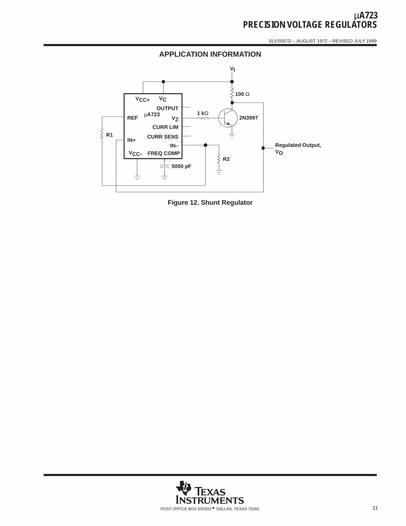
Figure 12. Shunt Regulator

PACKAGE OPTION ADDENDUM
www.ti.com 17-Mar-2017
Addendum-Page 1
PACKAGING INFORMATION
Orderable Device Status(1)
Package Type PackageDrawing
Pins PackageQty
Eco Plan(2)
Lead/Ball Finish(6)
MSL Peak Temp(3)
Op Temp (°C) Device Marking(4/5)
Samples
UA723CD ACTIVE SOIC D 14 50 Green (RoHS& no Sb/Br)
CU NIPDAU Level-1-260C-UNLIM 0 to 70 UA723C
UA723CDE4 ACTIVE SOIC D 14 50 Green (RoHS& no Sb/Br)
CU NIPDAU Level-1-260C-UNLIM 0 to 70 UA723C
UA723CDG4 ACTIVE SOIC D 14 50 Green (RoHS& no Sb/Br)
CU NIPDAU Level-1-260C-UNLIM 0 to 70 UA723C
UA723CDR ACTIVE SOIC D 14 2500 Green (RoHS& no Sb/Br)
CU NIPDAU Level-1-260C-UNLIM 0 to 70 UA723C
UA723CDRE4 ACTIVE SOIC D 14 2500 Green (RoHS& no Sb/Br)
CU NIPDAU Level-1-260C-UNLIM 0 to 70 UA723C
UA723CDRG4 ACTIVE SOIC D 14 2500 Green (RoHS& no Sb/Br)
CU NIPDAU Level-1-260C-UNLIM 0 to 70 UA723C
UA723CN ACTIVE PDIP N 14 25 Pb-Free(RoHS)
CU NIPDAU N / A for Pkg Type 0 to 70 UA723CN
UA723CNE4 ACTIVE PDIP N 14 25 Pb-Free(RoHS)
CU NIPDAU N / A for Pkg Type 0 to 70 UA723CN
UA723CNSR ACTIVE SO NS 14 2000 Green (RoHS& no Sb/Br)
CU NIPDAU Level-1-260C-UNLIM 0 to 70 UA723
(1) The marketing status values are defined as follows:ACTIVE: Product device recommended for new designs.LIFEBUY: TI has announced that the device will be discontinued, and a lifetime-buy period is in effect.NRND: Not recommended for new designs. Device is in production to support existing customers, but TI does not recommend using this part in a new design.PREVIEW: Device has been announced but is not in production. Samples may or may not be available.OBSOLETE: TI has discontinued the production of the device.
(2) Eco Plan - The planned eco-friendly classification: Pb-Free (RoHS), Pb-Free (RoHS Exempt), or Green (RoHS & no Sb/Br) - please check http://www.ti.com/productcontent for the latest availabilityinformation and additional product content details.TBD: The Pb-Free/Green conversion plan has not been defined.Pb-Free (RoHS): TI's terms "Lead-Free" or "Pb-Free" mean semiconductor products that are compatible with the current RoHS requirements for all 6 substances, including the requirement thatlead not exceed 0.1% by weight in homogeneous materials. Where designed to be soldered at high temperatures, TI Pb-Free products are suitable for use in specified lead-free processes.Pb-Free (RoHS Exempt): This component has a RoHS exemption for either 1) lead-based flip-chip solder bumps used between the die and package, or 2) lead-based die adhesive used betweenthe die and leadframe. The component is otherwise considered Pb-Free (RoHS compatible) as defined above.Green (RoHS & no Sb/Br): TI defines "Green" to mean Pb-Free (RoHS compatible), and free of Bromine (Br) and Antimony (Sb) based flame retardants (Br or Sb do not exceed 0.1% by weightin homogeneous material)

PACKAGE OPTION ADDENDUM
www.ti.com 17-Mar-2017
Addendum-Page 2
(3) MSL, Peak Temp. - The Moisture Sensitivity Level rating according to the JEDEC industry standard classifications, and peak solder temperature.
(4) There may be additional marking, which relates to the logo, the lot trace code information, or the environmental category on the device.
(5) Multiple Device Markings will be inside parentheses. Only one Device Marking contained in parentheses and separated by a "~" will appear on a device. If a line is indented then it is a continuationof the previous line and the two combined represent the entire Device Marking for that device.
(6) Lead/Ball Finish - Orderable Devices may have multiple material finish options. Finish options are separated by a vertical ruled line. Lead/Ball Finish values may wrap to two lines if the finishvalue exceeds the maximum column width.
Important Information and Disclaimer:The information provided on this page represents TI's knowledge and belief as of the date that it is provided. TI bases its knowledge and belief on informationprovided by third parties, and makes no representation or warranty as to the accuracy of such information. Efforts are underway to better integrate information from third parties. TI has taken andcontinues to take reasonable steps to provide representative and accurate information but may not have conducted destructive testing or chemical analysis on incoming materials and chemicals.TI and TI suppliers consider certain information to be proprietary, and thus CAS numbers and other limited information may not be available for release.
In no event shall TI's liability arising out of such information exceed the total purchase price of the TI part(s) at issue in this document sold by TI to Customer on an annual basis.

TAPE AND REEL INFORMATION
*All dimensions are nominal
Device PackageType
PackageDrawing
Pins SPQ ReelDiameter
(mm)
ReelWidth
W1 (mm)
A0(mm)
B0(mm)
K0(mm)
P1(mm)
W(mm)
Pin1Quadrant
UA723CDR SOIC D 14 2500 330.0 16.4 6.5 9.0 2.1 8.0 16.0 Q1
UA723CNSR SO NS 14 2000 330.0 16.4 8.2 10.5 2.5 12.0 16.0 Q1
PACKAGE MATERIALS INFORMATION
www.ti.com 14-Jul-2012
Pack Materials-Page 1

*All dimensions are nominal
Device Package Type Package Drawing Pins SPQ Length (mm) Width (mm) Height (mm)
UA723CDR SOIC D 14 2500 367.0 367.0 38.0
UA723CNSR SO NS 14 2000 367.0 367.0 38.0
PACKAGE MATERIALS INFORMATION
www.ti.com 14-Jul-2012
Pack Materials-Page 2


IMPORTANT NOTICE
Texas Instruments Incorporated (TI) reserves the right to make corrections, enhancements, improvements and other changes to itssemiconductor products and services per JESD46, latest issue, and to discontinue any product or service per JESD48, latest issue. Buyersshould obtain the latest relevant information before placing orders and should verify that such information is current and complete.TI’s published terms of sale for semiconductor products (http://www.ti.com/sc/docs/stdterms.htm) apply to the sale of packaged integratedcircuit products that TI has qualified and released to market. Additional terms may apply to the use or sale of other types of TI products andservices.Reproduction of significant portions of TI information in TI data sheets is permissible only if reproduction is without alteration and isaccompanied by all associated warranties, conditions, limitations, and notices. TI is not responsible or liable for such reproduceddocumentation. Information of third parties may be subject to additional restrictions. Resale of TI products or services with statementsdifferent from or beyond the parameters stated by TI for that product or service voids all express and any implied warranties for theassociated TI product or service and is an unfair and deceptive business practice. TI is not responsible or liable for any such statements.Buyers and others who are developing systems that incorporate TI products (collectively, “Designers”) understand and agree that Designersremain responsible for using their independent analysis, evaluation and judgment in designing their applications and that Designers havefull and exclusive responsibility to assure the safety of Designers' applications and compliance of their applications (and of all TI productsused in or for Designers’ applications) with all applicable regulations, laws and other applicable requirements. Designer represents that, withrespect to their applications, Designer has all the necessary expertise to create and implement safeguards that (1) anticipate dangerousconsequences of failures, (2) monitor failures and their consequences, and (3) lessen the likelihood of failures that might cause harm andtake appropriate actions. Designer agrees that prior to using or distributing any applications that include TI products, Designer willthoroughly test such applications and the functionality of such TI products as used in such applications.TI’s provision of technical, application or other design advice, quality characterization, reliability data or other services or information,including, but not limited to, reference designs and materials relating to evaluation modules, (collectively, “TI Resources”) are intended toassist designers who are developing applications that incorporate TI products; by downloading, accessing or using TI Resources in anyway, Designer (individually or, if Designer is acting on behalf of a company, Designer’s company) agrees to use any particular TI Resourcesolely for this purpose and subject to the terms of this Notice.TI’s provision of TI Resources does not expand or otherwise alter TI’s applicable published warranties or warranty disclaimers for TIproducts, and no additional obligations or liabilities arise from TI providing such TI Resources. TI reserves the right to make corrections,enhancements, improvements and other changes to its TI Resources. TI has not conducted any testing other than that specificallydescribed in the published documentation for a particular TI Resource.Designer is authorized to use, copy and modify any individual TI Resource only in connection with the development of applications thatinclude the TI product(s) identified in such TI Resource. NO OTHER LICENSE, EXPRESS OR IMPLIED, BY ESTOPPEL OR OTHERWISETO ANY OTHER TI INTELLECTUAL PROPERTY RIGHT, AND NO LICENSE TO ANY TECHNOLOGY OR INTELLECTUAL PROPERTYRIGHT OF TI OR ANY THIRD PARTY IS GRANTED HEREIN, including but not limited to any patent right, copyright, mask work right, orother intellectual property right relating to any combination, machine, or process in which TI products or services are used. Informationregarding or referencing third-party products or services does not constitute a license to use such products or services, or a warranty orendorsement thereof. Use of TI Resources may require a license from a third party under the patents or other intellectual property of thethird party, or a license from TI under the patents or other intellectual property of TI.TI RESOURCES ARE PROVIDED “AS IS” AND WITH ALL FAULTS. TI DISCLAIMS ALL OTHER WARRANTIES ORREPRESENTATIONS, EXPRESS OR IMPLIED, REGARDING RESOURCES OR USE THEREOF, INCLUDING BUT NOT LIMITED TOACCURACY OR COMPLETENESS, TITLE, ANY EPIDEMIC FAILURE WARRANTY AND ANY IMPLIED WARRANTIES OFMERCHANTABILITY, FITNESS FOR A PARTICULAR PURPOSE, AND NON-INFRINGEMENT OF ANY THIRD PARTY INTELLECTUALPROPERTY RIGHTS. TI SHALL NOT BE LIABLE FOR AND SHALL NOT DEFEND OR INDEMNIFY DESIGNER AGAINST ANY CLAIM,INCLUDING BUT NOT LIMITED TO ANY INFRINGEMENT CLAIM THAT RELATES TO OR IS BASED ON ANY COMBINATION OFPRODUCTS EVEN IF DESCRIBED IN TI RESOURCES OR OTHERWISE. IN NO EVENT SHALL TI BE LIABLE FOR ANY ACTUAL,DIRECT, SPECIAL, COLLATERAL, INDIRECT, PUNITIVE, INCIDENTAL, CONSEQUENTIAL OR EXEMPLARY DAMAGES INCONNECTION WITH OR ARISING OUT OF TI RESOURCES OR USE THEREOF, AND REGARDLESS OF WHETHER TI HAS BEENADVISED OF THE POSSIBILITY OF SUCH DAMAGES.Unless TI has explicitly designated an individual product as meeting the requirements of a particular industry standard (e.g., ISO/TS 16949and ISO 26262), TI is not responsible for any failure to meet such industry standard requirements.Where TI specifically promotes products as facilitating functional safety or as compliant with industry functional safety standards, suchproducts are intended to help enable customers to design and create their own applications that meet applicable functional safety standardsand requirements. Using products in an application does not by itself establish any safety features in the application. Designers mustensure compliance with safety-related requirements and standards applicable to their applications. Designer may not use any TI products inlife-critical medical equipment unless authorized officers of the parties have executed a special contract specifically governing such use.Life-critical medical equipment is medical equipment where failure of such equipment would cause serious bodily injury or death (e.g., lifesupport, pacemakers, defibrillators, heart pumps, neurostimulators, and implantables). Such equipment includes, without limitation, allmedical devices identified by the U.S. Food and Drug Administration as Class III devices and equivalent classifications outside the U.S.TI may expressly designate certain products as completing a particular qualification (e.g., Q100, Military Grade, or Enhanced Product).Designers agree that it has the necessary expertise to select the product with the appropriate qualification designation for their applicationsand that proper product selection is at Designers’ own risk. Designers are solely responsible for compliance with all legal and regulatoryrequirements in connection with such selection.Designer will fully indemnify TI and its representatives against any damages, costs, losses, and/or liabilities arising out of Designer’s non-compliance with the terms and provisions of this Notice.
Mailing Address: Texas Instruments, Post Office Box 655303, Dallas, Texas 75265Copyright © 2017, Texas Instruments Incorporated