Embed Size (px)
Citation preview
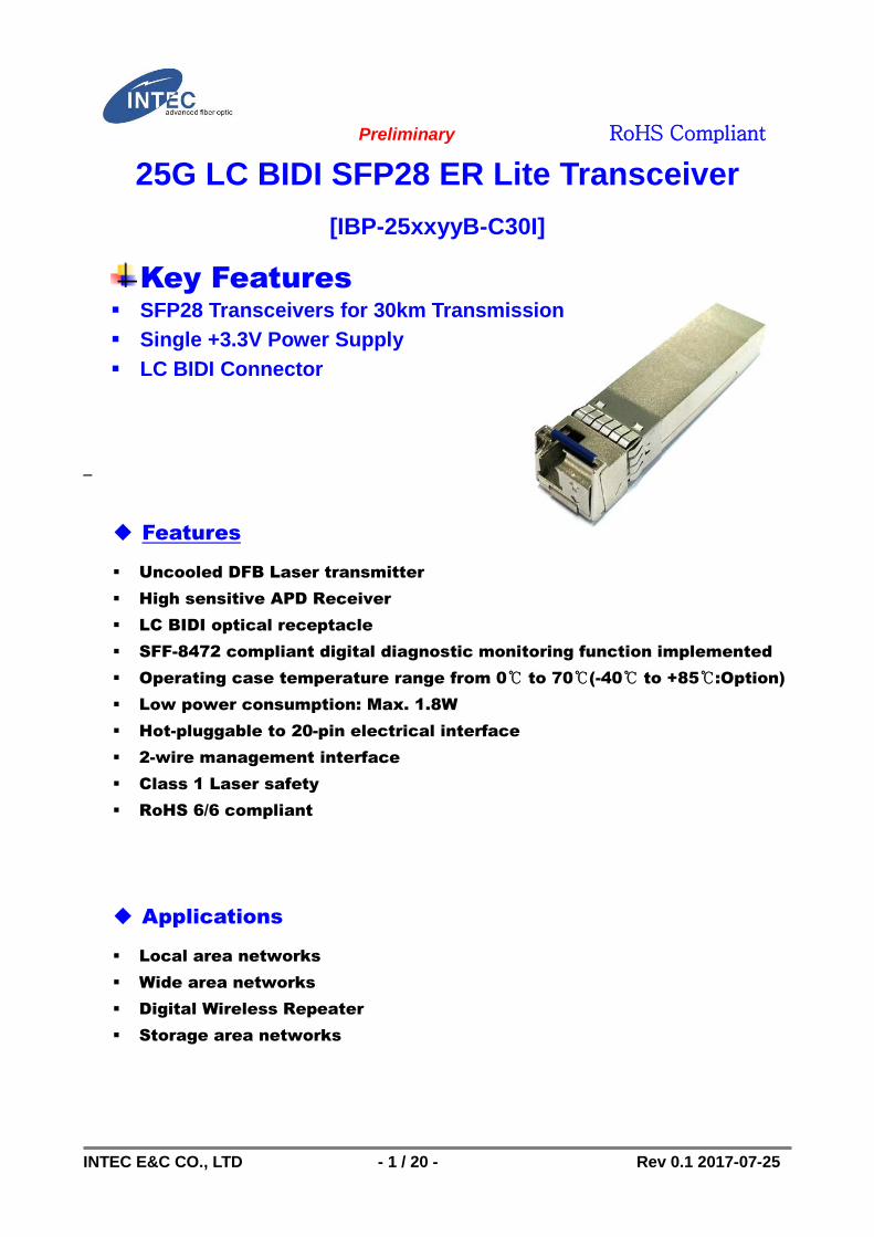
Preliminary RoHS Compliant
INTEC E&C CO., LTD - 1 / 20 - Rev 0.1 2017-07-25
25G LC BIDI SFP28 ER Lite Transceiver
[IBP-25xxyyB-C30I]
Features
Uncooled DFB Laser transmitter
High sensitive APD Receiver
LC BIDI optical receptacle
SFF-8472 compliant digital diagnostic monitoring function implemented
Operating case temperature range from 0℃ to 70℃(-40℃ to +85℃:Option)
Low power consumption: Max. 1.8W
Hot-pluggable to 20-pin electrical interface
2-wire management interface
Class 1 Laser safety
RoHS 6/6 compliant
Applications
Local area networks
Wide area networks
Digital Wireless Repeater
Storage area networks
Key Features SFP28 Transceivers for 30km Transmission
Single +3.3V Power Supply
LC BIDI Connector
Preliminary RoHS Compliant
INTEC E&C CO., LTD - 2 / 20 - Rev. 0.1 2017-07-25
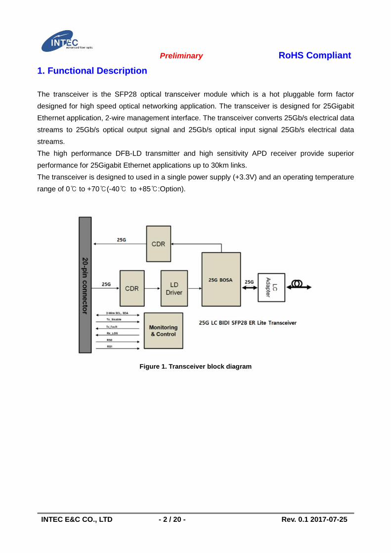
1. Functional Description
The transceiver is the SFP28 optical transceiver module which is a hot pluggable form factor
designed for high speed optical networking application. The transceiver is designed for 25Gigabit
Ethernet application, 2-wire management interface. The transceiver converts 25Gb/s electrical data
streams to 25Gb/s optical output signal and 25Gb/s optical input signal 25Gb/s electrical data
streams.
The high performance DFB-LD transmitter and high sensitivity APD receiver provide superior
performance for 25Gigabit Ethernet applications up to 30km links.
The transceiver is designed to used in a single power supply (+3.3V) and an operating temperature
range of 0℃ to +70℃(-40℃ to +85℃:Option).
Figure 1. Transceiver block diagram
Preliminary RoHS Compliant
INTEC E&C CO., LTD - 3 / 20 - Rev. 0.1 2017-07-25
1.1 Low Speed Description
1.1.1 Low Speed Pin Descriptions
The transceiver has several low-speed interface connectors including a 2-wire serial interface (SCL
and SDA). These connections include: Tx_Fault, Tx_Disable, RS0/RS1, Mod_ABS, Rx_LOS.
[Tx_Fault]
Tx_Fault is a module output that when high, indicates that the module transmitter has detected a
fault condition related to laser operation or safety. If Tx_Fault is not implemented, the Tx_Fault
contact signal shall be held low by the module and may be connected to Vee within the module.
The Tx_Fault output is an open drain/collector and shall be pulled up to the Vcc_Host in the host
with a resistor in the range 4.7 kOhms to 10 kOhms.
[Tx_Disable]
When Tx_Disable is asserted high or left open, the SFP+ module transmitter output shall be turned
off unless the module is a passive cable assembly (see Appendix E in SFF-8419) in which case
this signal may be ignored. This contact shall be pulled up to VccT with a 4.7 kOhms to 10 kOhms
resistor in modules and cable assemblies.
Tx_Disable is a module input contact. When Tx_Disable is asserted low or grounded the module
transmitter is operating normally.
[RS0/RS1]
RS0 and RS1 are module inputs and are pulled low to VeeT with >30 kOhms resistors in the
module. RS0 optionally selects the optical receive signaling rate coverage. RS1 optionally selects
the optical transmit signaling rate coverage. For logical definitions of RS0/RS1 see Section 4.2.
These contacts can also be used for AS0 and AS1 if implementing SFF-8079. See SFF- 8079 for
details.
RS1 is commonly connected to VeeT or VeeR in the classic SFP modules. The host needs to
ensure that it will not be damaged if this contact is connected to VeeT or VeeR in the module.
[Mod_ABS]
Mod_ABS is connected to VeeT or VeeR in the SFP+ module. The host may pull this contact up to
Vcc_Host with a resistor in the range 4.7 kOhms to 10 kOhms. Mod_ABS is asserted 'High' when
the SFP+ module is physically absent from a host slot. In the SFP MSA (INF-8074i) this contact
has the same function but is called MOD_DEF0.
[Rx_LOS]
Rx_LOS when high indicates an optical signal level below that specified in the relevant standard.
Preliminary RoHS Compliant
INTEC E&C CO., LTD - 4 / 20 - Rev. 0.1 2017-07-25
Rx_LOS is an open drain/collector output, but may also be used as an input by supervisory
circuitry in the module. For a nominally 3.3 V Vcc_Host using a resistive pull up to Vcc_Host the
resistor value shall be in the range 4.7kOhms to 10 kOhms. For a nominally 2.5 V Vcc_Host using
a resistive pull up to Vcc_Host the resistor value shall be in the range 4.7 kOhms to 7.2 kOhms.
The Rx_LOS signal is intended as a preliminary indication to the host in which the module is
installed that the received signal strength is below the specified range. Such an indication typically
points to non-installed cables, broken cables, or a disabled, failing or a powered off transmitter at
the far end of the cable.
Additional indications are provided by the host in which the module is installed to verify that the
information being transmitted is valid, correctly encoded, and in the correct format. Such additional
indications are outside the scope of the module specification.
Rx_LOS may be an optional function depending on the supported standard. If the Rx_LOS function
is not implemented, or is reported via the two-wire interface only, the Rx_LOS contact shall be held
low by the module and may be connected to Vee within the module.
Rx_LOS assert min and de-assert max are defined in the relevant standard. To avoid spurious
transition of Rx_LOS a minimum hysteresis of 0.5 dBo is recommended.
1.1.1 Low Speed Pin Electrical Specifications
[Low Speed Signaling]
Low speed signaling other than SCL and SDA is based on Low Voltage TTL (LVTTL) operating at
Vcc. Vcc refers to the generic supply voltages of VccTx, VccRx, Vcc_host or Vcc1.
Hosts shall use a pull-up resistor connected to Vcc_host on each of the 2-wire interface SCL
(clock), SDA (data), and all low speed status outputs.
The SCL and SDA is a hot plug interface that may support a bus topology. During module insertion
or removal, the module may implement a pre-charge circuit which prevents corrupting data
transfers from other modules that are already using the bus.
Table 1. Low Speed Pin Electrical Specifications
Parameter Symbol Min Max Unit Condition
Host 2-wire Vcc Vcc_Host_2w 3.14 3.46 V
SCL and SDA
VOL 0.0 0.4 V Rp2w 2 pulled to
Vcc_Host_2w
VOH Vcc_Host_2w
-0.5
Vcc_Host_2w
+0.3 V
Rp2w 2 pulled to
Vcc_Host_2w
SCL and SDA VIL -0.3 VccT*0.3 V
VIH VccT*0.7 VccT+0.5 V
Capacitance for SCL and SDA I/O Ci 14 pF
Preliminary RoHS Compliant
INTEC E&C CO., LTD - 5 / 20 - Rev. 0.1 2017-07-25
Pin
Total bus capacitive load for SCL
and SDA Cb
100 pF 3.0KΩ Pull-up resistor, Max
200 pF 1.6KΩ Pull-up resistor, Max
LPMode, Reset and ModSelL VIL -0.3 0.8 V |Iin|<=125uA for 0V<Vin, Vcc
VIH 2 Vcc+0.3 V
ModPrsL and IntL VOL 0 0.4 V IOL=2.0mA
VOH Vcc-0.5 Vcc+0.3 V
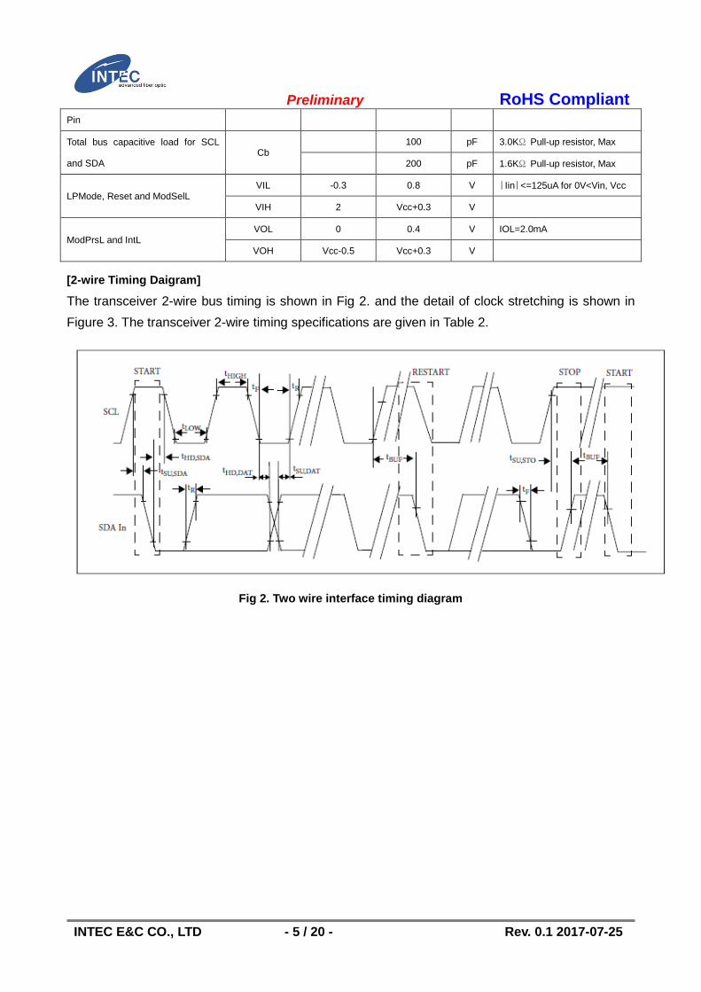
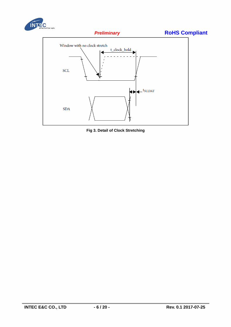
[2-wire Timing Daigram]
The transceiver 2-wire bus timing is shown in Fig 2. and the detail of clock stretching is shown in
Figure 3. The transceiver 2-wire timing specifications are given in Table 2.
Fig 2. Two wire interface timing diagram
Preliminary RoHS Compliant
INTEC E&C CO., LTD - 6 / 20 - Rev. 0.1 2017-07-25
Fig 3. Detail of Clock Stretching
Preliminary RoHS Compliant
INTEC E&C CO., LTD - 7 / 20 - Rev. 0.1 2017-07-25
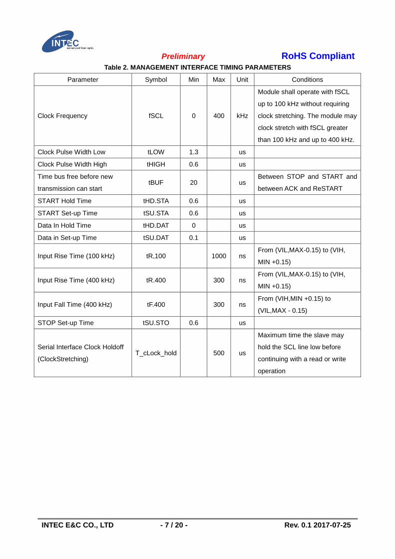
Table 2. MANAGEMENT INTERFACE TIMING PARAMETERS
Parameter Symbol Min Max Unit Conditions
Clock Frequency fSCL 0 400 kHz
Module shall operate with fSCL
up to 100 kHz without requiring
clock stretching. The module may
clock stretch with fSCL greater
than 100 kHz and up to 400 kHz.
Clock Pulse Width Low tLOW 1.3 us
Clock Pulse Width High tHIGH 0.6 us
Time bus free before new
transmission can start tBUF 20 us
Between STOP and START and
between ACK and ReSTART
START Hold Time tHD.STA 0.6 us
START Set-up Time tSU.STA 0.6 us
Data In Hold Time tHD.DAT 0 us
Data in Set-up Time tSU.DAT 0.1 us
Input Rise Time (100 kHz) tR,100 1000 ns From (VIL,MAX-0.15) to (VIH,
MIN +0.15)
Input Rise Time (400 kHz) tR.400 300 ns From (VIL,MAX-0.15) to (VIH,
MIN +0.15)
Input Fall Time (400 kHz) tF.400 300 ns From (VIH,MIN +0.15) to
(VIL,MAX - 0.15)
STOP Set-up Time tSU.STO 0.6 us
Serial Interface Clock Holdoff
(ClockStretching) T_cLock_hold 500 us
Maximum time the slave may
hold the SCL line low before
continuing with a read or write
operation
Preliminary RoHS Compliant
INTEC E&C CO., LTD - 8 / 20 - Rev. 0.1 2017-07-25
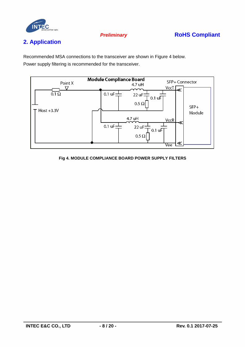
2. Application
Recommended MSA connections to the transceiver are shown in Figure 4 below.
Power supply filtering is recommended for the transceiver.
Fig 4. MODULE COMPLIANCE BOARD POWER SUPPLY FILTERS
Preliminary RoHS Compliant
INTEC E&C CO., LTD - 9 / 20 - Rev. 0.1 2017-07-25
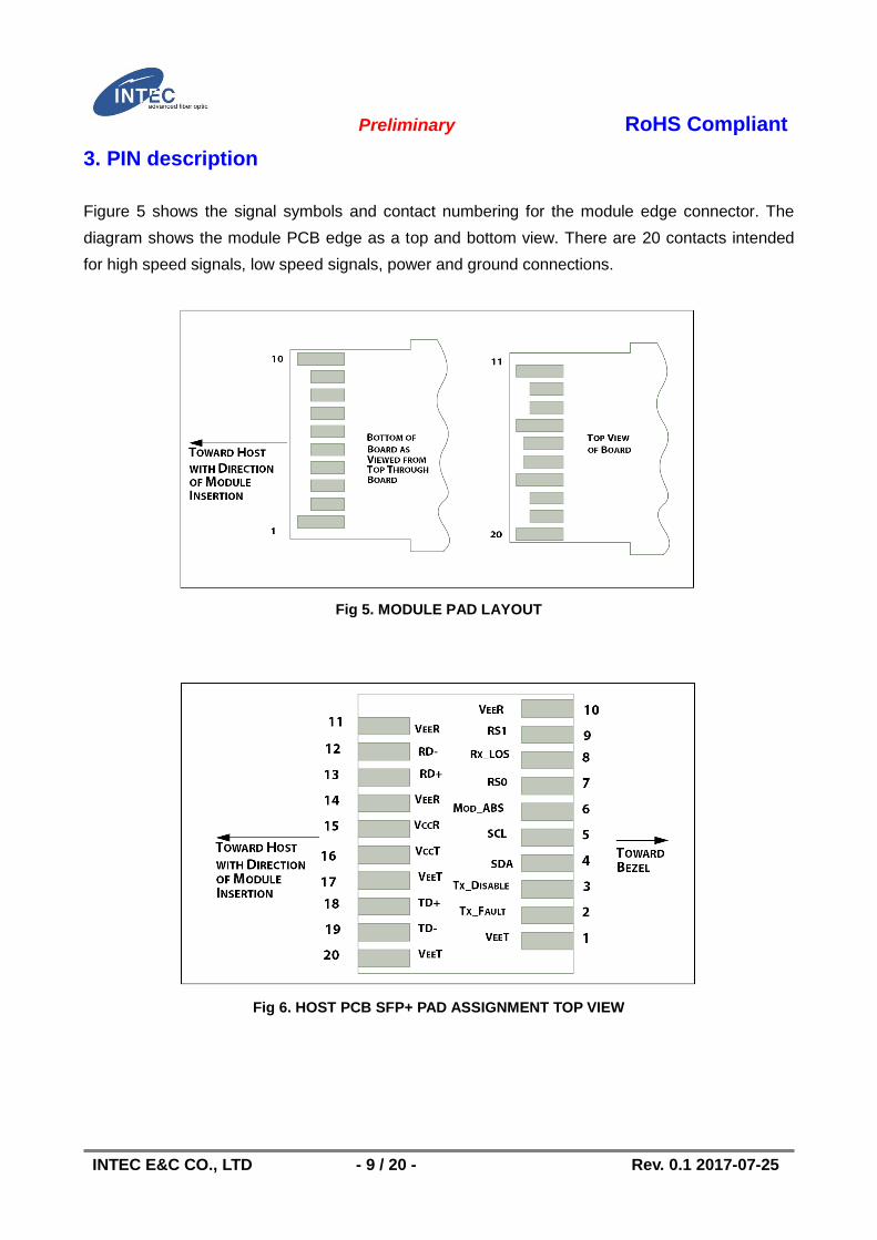
3. PIN description
Figure 5 shows the signal symbols and contact numbering for the module edge connector. The
diagram shows the module PCB edge as a top and bottom view. There are 20 contacts intended
for high speed signals, low speed signals, power and ground connections.
Fig 5. MODULE PAD LAYOUT
Fig 6. HOST PCB SFP+ PAD ASSIGNMENT TOP VIEW
Preliminary RoHS Compliant
INTEC E&C CO., LTD - 10 / 20 - Rev. 0.1 2017-07-25
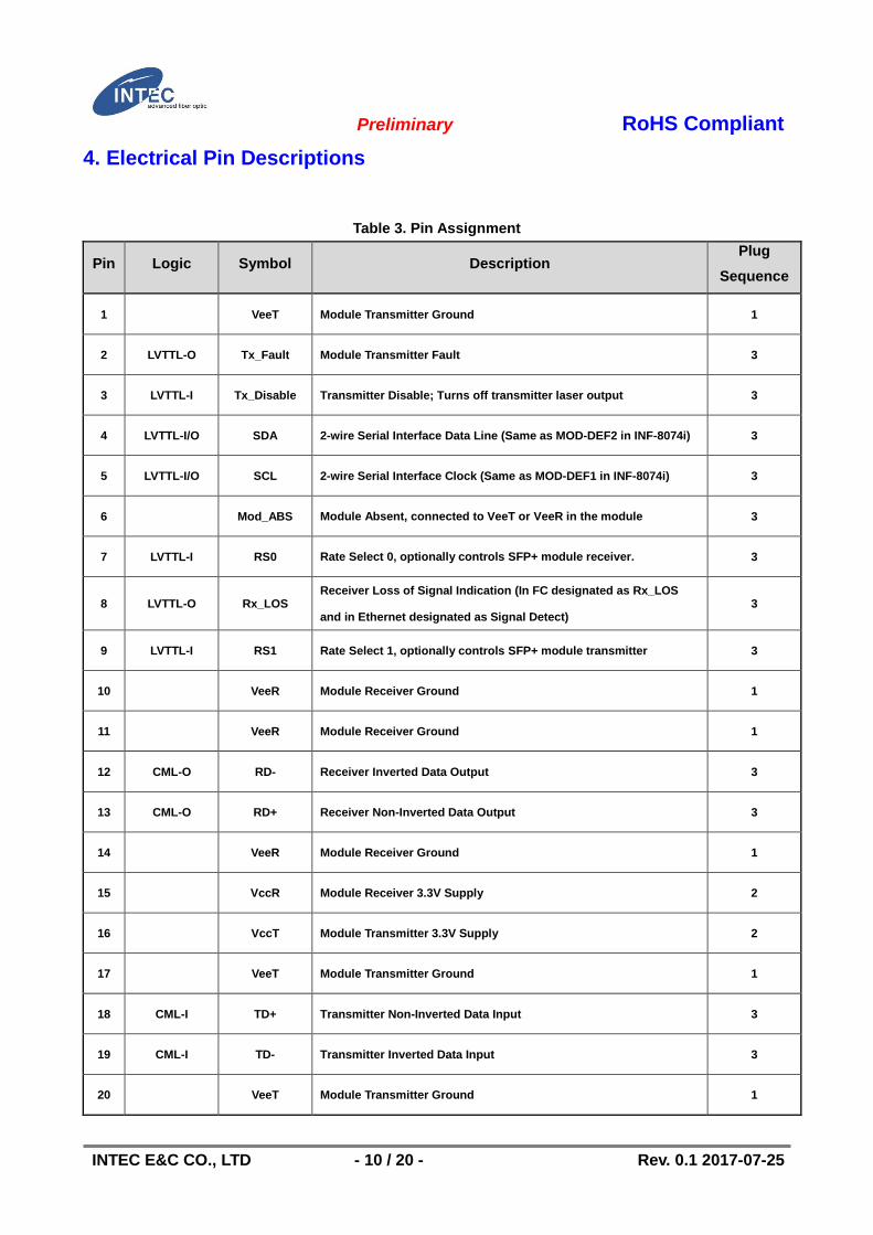
4. Electrical Pin Descriptions
Table 3. Pin Assignment
Pin Logic Symbol Description Plug
Sequence
1 VeeT Module Transmitter Ground 1
2 LVTTL-O Tx_Fault Module Transmitter Fault 3
3 LVTTL-I Tx_Disable Transmitter Disable; Turns off transmitter laser output 3
4 LVTTL-I/O SDA 2-wire Serial Interface Data Line (Same as MOD-DEF2 in INF-8074i) 3
5 LVTTL-I/O SCL 2-wire Serial Interface Clock (Same as MOD-DEF1 in INF-8074i) 3
6 Mod_ABS Module Absent, connected to VeeT or VeeR in the module 3
7 LVTTL-I RS0 Rate Select 0, optionally controls SFP+ module receiver. 3
8 LVTTL-O Rx_LOS Receiver Loss of Signal Indication (In FC designated as Rx_LOS
and in Ethernet designated as Signal Detect) 3
9 LVTTL-I RS1 Rate Select 1, optionally controls SFP+ module transmitter 3
10 VeeR Module Receiver Ground 1
11 VeeR Module Receiver Ground 1
12 CML-O RD- Receiver Inverted Data Output 3
13 CML-O RD+ Receiver Non-Inverted Data Output 3
14 VeeR Module Receiver Ground 1
15 VccR Module Receiver 3.3V Supply 2
16 VccT Module Transmitter 3.3V Supply 2
17 VeeT Module Transmitter Ground 1
18 CML-I TD+ Transmitter Non-Inverted Data Input 3
19 CML-I TD- Transmitter Inverted Data Input 3
20 VeeT Module Transmitter Ground 1
Preliminary RoHS Compliant
INTEC E&C CO., LTD - 11 / 20 - Rev. 0.1 2017-07-25
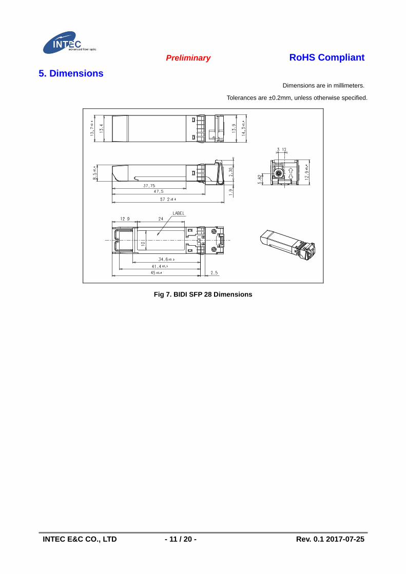
5. Dimensions Dimensions are in millimeters.
Tolerances are ±0.2mm, unless otherwise specified.
Fig 7. BIDI SFP 28 Dimensions
Preliminary RoHS Compliant
INTEC E&C CO., LTD - 12 / 20 - Rev. 0.1 2017-07-25
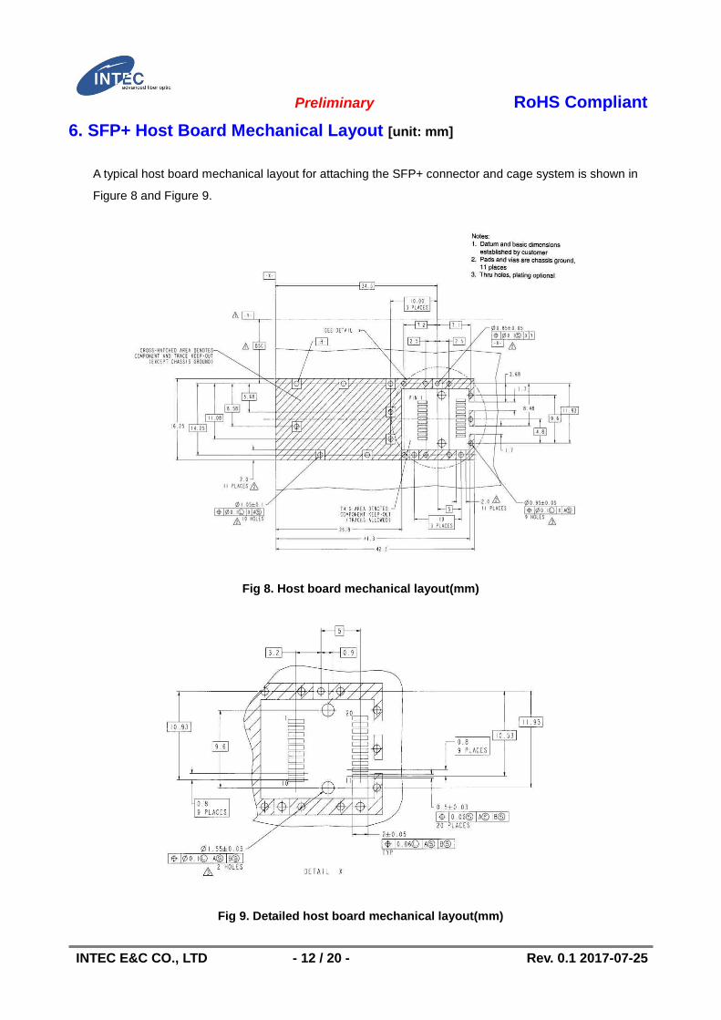
6. SFP+ Host Board Mechanical Layout [unit: mm]
A typical host board mechanical layout for attaching the SFP+ connector and cage system is shown in
Figure 8 and Figure 9.
Fig 8. Host board mechanical layout(mm)
Fig 9. Detailed host board mechanical layout(mm)
Preliminary RoHS Compliant
INTEC E&C CO., LTD - 13 / 20 - Rev. 0.1 2017-07-25
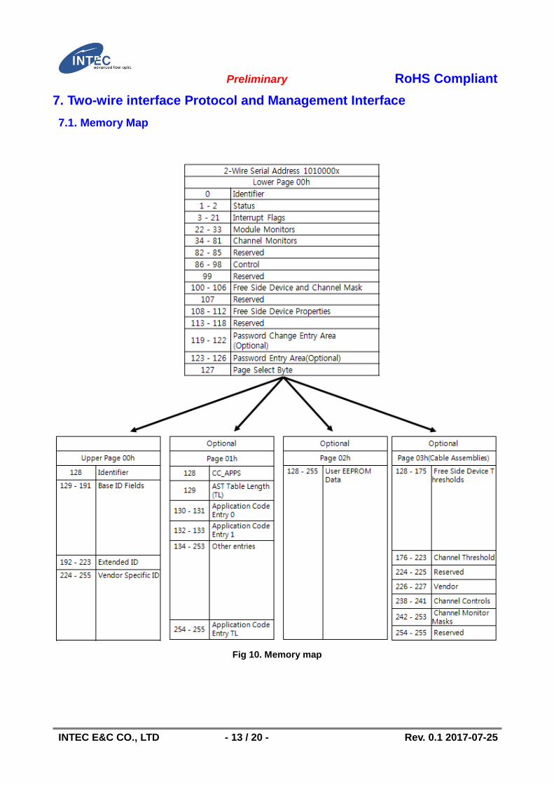
7. Two-wire interface Protocol and Management Interface
7.1. Memory Map
Fig 10. Memory map
Preliminary RoHS Compliant
INTEC E&C CO., LTD - 14 / 20 - Rev. 0.1 2017-07-25
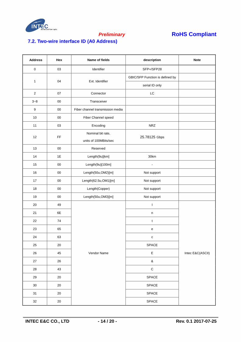
7.2. Two-wire interface ID (A0 Address)
Address Hex Name of fields description Note
0 03 Identifier SFP+/SFP28
1 04 Ext. Identifier
GBIC/SFP Function is defined by
serial ID only
2 07 Connector LC
3~8 00 Transceiver
9 00 Fiber channel transmission media
10 00 Fiber Channel speed
11 03 Encoding NRZ
12 FF Nominal bit rate,
units of 100MBits/sec 25.78125 Gbps
13 00 Reserved
14 1E Length(9u)[km] 30km
15 00 Length(9u)[100m] -
16 00 Length(50u,OM2)[m] Not support
17 00 Length(62.5u,OM1)[m] Not support
18 00 Length(Copper) Not support
19 00 Length(50u,OM3)[m] Not support
20 49
Vendor Name
I
Intec E&C(ASCII)
21 6E n
22 74 t
23 65 e
24 63 c
25 20 SPACE
26 45 E
27 26 &
28 43 C
29 20 SPACE
30 20 SPACE
31 20 SPACE
32 20 SPACE
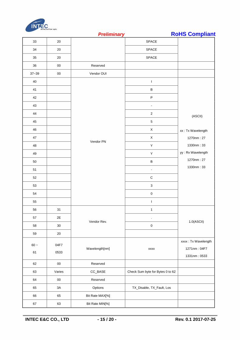
Preliminary RoHS Compliant
INTEC E&C CO., LTD - 15 / 20 - Rev. 0.1 2017-07-25
33 20 SPACE
34 20 SPACE
35 20 SPACE
36 00 Reserved
37~39 00 Vendor OUI
40
Vendor PN
I
(ASCII)
xx : Tx Wavelength
1270nm : 27
1330nm : 33
yy : Rx Wavelength
1270nm : 27
1330nm : 33
41 B
42 P
43 -
44 2
45 5
46 X
47 X
48 Y
49 Y
50 B
51 -
52 C
53 3
54 0
55 I
56 31
Vendor Rev.
1
1.0(ASCII)
57 2E .
58 30 0
59 20
60 ~
61
04F7
0533 Wavelength[nm] xxxx
xxxx : Tx Wavelength
1271nm : 04F7
1331nm : 0533
62 00 Reserved
63 Varies CC_BASE Check Sum byte for Bytes 0 to 62
64 00 Reserved
65 3A Options TX_Disable, TX_Fault, Los
66 65 Bit Rate MAX[%]
67 63 Bit Rate MIN[%]
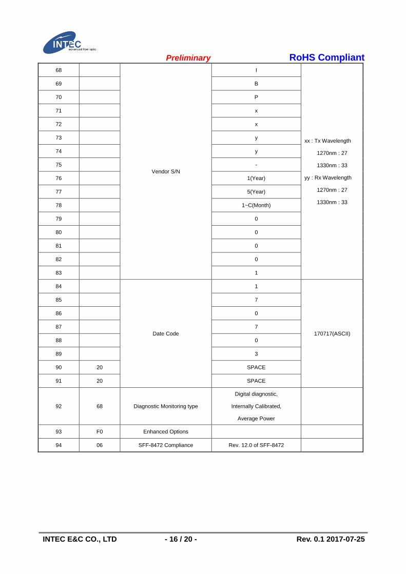
Preliminary RoHS Compliant
INTEC E&C CO., LTD - 16 / 20 - Rev. 0.1 2017-07-25
68
Vendor S/N
I
xx : Tx Wavelength
1270nm : 27
1330nm : 33
yy : Rx Wavelength
1270nm : 27
1330nm : 33
69 B
70 P
71 x
72 x
73 y
74 y
75 -
76 1(Year)
77 5(Year)
78 1~C(Month)
79 0
80 0
81 0
82 0
83 1
84
Date Code
1
170717(ASCII)
85 7
86 0
87 7
88 0
89 3
90 20 SPACE
91 20 SPACE
92 68 Diagnostic Monitoring type
Digital diagnostic,
Internally Calibrated,
Average Power
93 F0 Enhanced Options
94 06 SFF-8472 Compliance Rev. 12.0 of SFF-8472
Preliminary RoHS Compliant
INTEC E&C CO., LTD - 17 / 20 - Rev. 0.1 2017-07-25
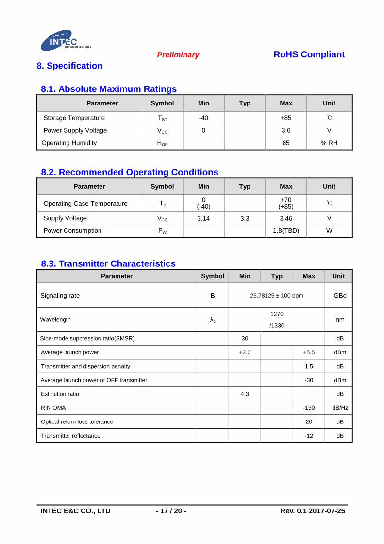
8. Specification
8.1. Absolute Maximum Ratings
Parameter Symbol Min Typ Max Unit
Storage Temperature TST -40 +85 ℃
Power Supply Voltage VCC 0 3.6 V
Operating Humidity HOP 85 % RH
8.2. Recommended Operating Conditions
Parameter Symbol Min Typ Max Unit
Operating Case Temperature Tc 0
(-40)
+70 (+85)
℃
Supply Voltage VCC 3.14 3.3 3.46 V
Power Consumption PW 1.8(TBD) W
8.3. Transmitter Characteristics
Parameter Symbol Min Typ Max Unit
Signaling rate B
25.78125 ± 100 ppm GBd
Wavelength λc 1270
/1330 nm
Side-mode suppression ratio(SMSR) 30 dB
Average launch power +2.0 +5.5 dBm
Transmitter and dispersion penalty 1.5 dB
Average launch power of OFF transmitter -30 dBm
Extinction ratio 4.3 dB
RIN OMA -130 dB/Hz
Optical return loss tolerance 20 dB
Transmitter reflectance -12 dB
Preliminary RoHS Compliant
INTEC E&C CO., LTD - 18 / 20 - Rev. 0.1 2017-07-25
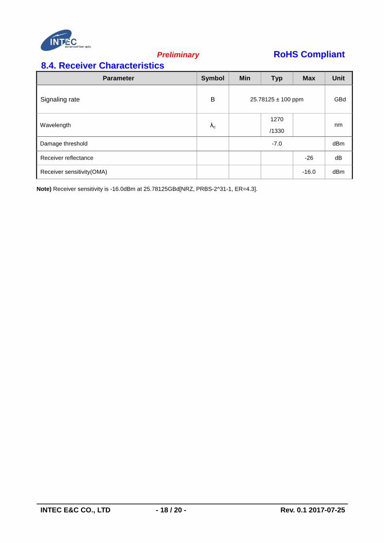
8.4. Receiver Characteristics
Parameter Symbol Min Typ Max Unit
Signaling rate B
25.78125 ± 100 ppm GBd
Wavelength λc 1270
/1330 nm
Damage threshold -7.0 dBm
Receiver reflectance -26 dB
Receiver sensitivity(OMA) -16.0 dBm
Note) Receiver sensitivity is -16.0dBm at 25.78125GBd[NRZ, PRBS-2^31-1, ER=4.3].
Preliminary RoHS Compliant
INTEC E&C CO., LTD - 19 / 20 - Rev. 0.1 2017-07-25
9. ESD(Electrostatic Discharge)
The module speed signal contacts shall withstand 1000 V electrostatic discharge based on Human
Body Model per JEDEC JESD22-A114-B.
10, Laser Safety
The transceivers use a semiconductor laser that is classified as Class 1 laser products per the
laser safety requirements of FDA/CDRH, 21 CFR1040.10 and 1040.11. These products have also
been tested and certified as Class 1 laser products per IEC60825-1:2007 and IEC60825-1:2001
International standards.
Preliminary RoHS Compliant
INTEC E&C CO., LTD - 20 / 20 - Rev. 0.1 2017-07-25
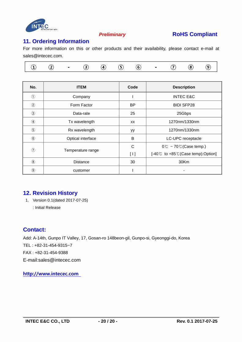
11. Ordering Information
For more information on this or other products and their availability, please contact e-mail at
No. ITEM Code Description
① Company I INTEC E&C
② Form Factor BP BIDI SFP28
③ Data-rate 25 25Gbps
④ Tx wavelength xx 1270nm/1330nm
⑤ Rx wavelength yy 1270nm/1330nm
⑥ Optical interface B LC-UPC receptacle
⑦ Temperature range C
[ I ]
0℃ ~ 70℃(Case temp.)
[-40℃ to +85℃(Case temp):Option]
⑧ Distance 30 30Km
⑨ customer I -
12. Revision History 1. Version 0.1(dated 2017-07-25)
: Initial Release
Contact:
Add: A-14th, Gunpo IT Valley, 17, Gosan-ro 148beon-gil, Gunpo-si, Gyeonggi-do, Korea
TEL : +82-31-454-9315~7
FAX : +82-31-454-9388
E-mail:[email protected]
http://www.intecec.com