Embed Size (px)
Citation preview

This document is owned by Agilent Technologies, but is no longer kept current and may contain obsolete or
inaccurate references. We regret any inconvenience this may cause. For the latest information on Agilent’s
line of EEsof electronic design automation (EDA) products and services, please go to:
www.agilent.com/fi nd/eesof
Agilent EEsof EDA
1Agilent Technologies
Invited seminar presentation at the Technische Universität München,Lehrstuhl für Technische Elektronik
Prof. Schmitt-Landsiedel
28. January 2003
Note: in the handouts, please find the notes below the corresponding slides. Slide 2
2Agilent Technologies
Author: [email protected]
Basics of DC and AC Characterization
of Semiconductors
Agilent Technologies
The trend to higher integration and higher transmission speed challenges modeling engineers to develop accurate device models up to the Gigahertz range. An absolute prerequisite for achieving this goal are reliable measurements, which have to be checked for data consistency and plausibility. This is especially true for radio-frequency (RF, >100MHz) and microwave (GHz) measurements, and also for checking and verifying the applied de-embedding techniques. If there are (hidden) problems with the measurement data, RF characterizations can become quite time consuming, with a lot of guesswork and ad-hoc judgments, and, basically, frustrating and not correct. If, however, the underlying measurements are flawless and consistent, and provided the applied the models are understood well, RF characterization and device modeling becomes very effective and provides accurate design kits which will satisfy the chip designer's main goal: right the fist time.
Slide 3
3Agilent Technologies
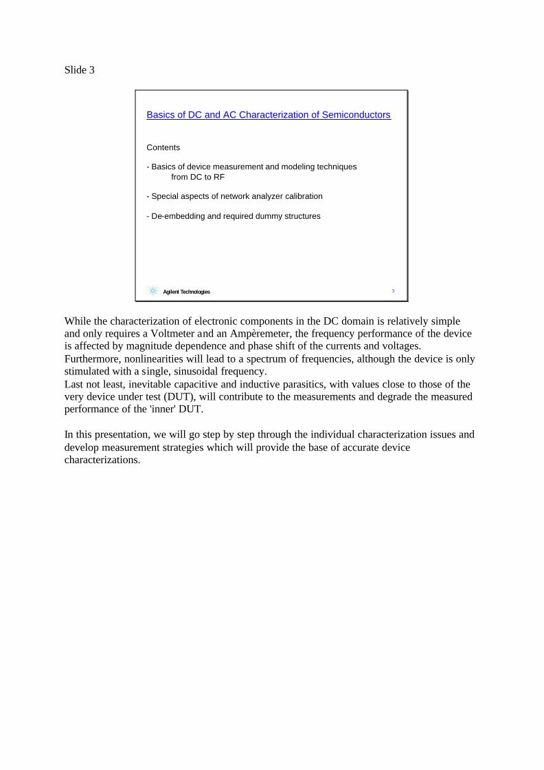
Basics of DC and AC Characterization of Semiconductors
Contents
- Basics of device measurement and modeling techniques from DC to RF
- Special aspects of network analyzer calibration
- De-embedding and required dummy structures
While the characterization of electronic components in the DC domain is relatively simple and only requires a Voltmeter and an Ampèremeter, the frequency performance of the device is affected by magnitude dependence and phase shift of the currents and voltages. Furthermore, nonlinearities will lead to a spectrum of frequencies, although the device is only stimulated with a single, sinusoidal frequency. Last not least, inevitable capacitive and inductive parasitics, with values close to those of the very device under test (DUT), will contribute to the measurements and degrade the measured performance of the 'inner' DUT. In this presentation, we will go step by step through the individual characterization issues and develop measurement strategies which will provide the base of accurate device characterizations.
Slide 4
4Agilent Technologies
Basics of DC and AC Characterization of Semiconductors
Contents
- Basics of device measurement and modeling techniques from DC to RF
- Special aspects of network analyzer calibration
- De-embedding and required dummy structures
Let’s begin with the basics of measurement techniques and device modeling from DC to RF. Slide 5
5Agilent Technologies
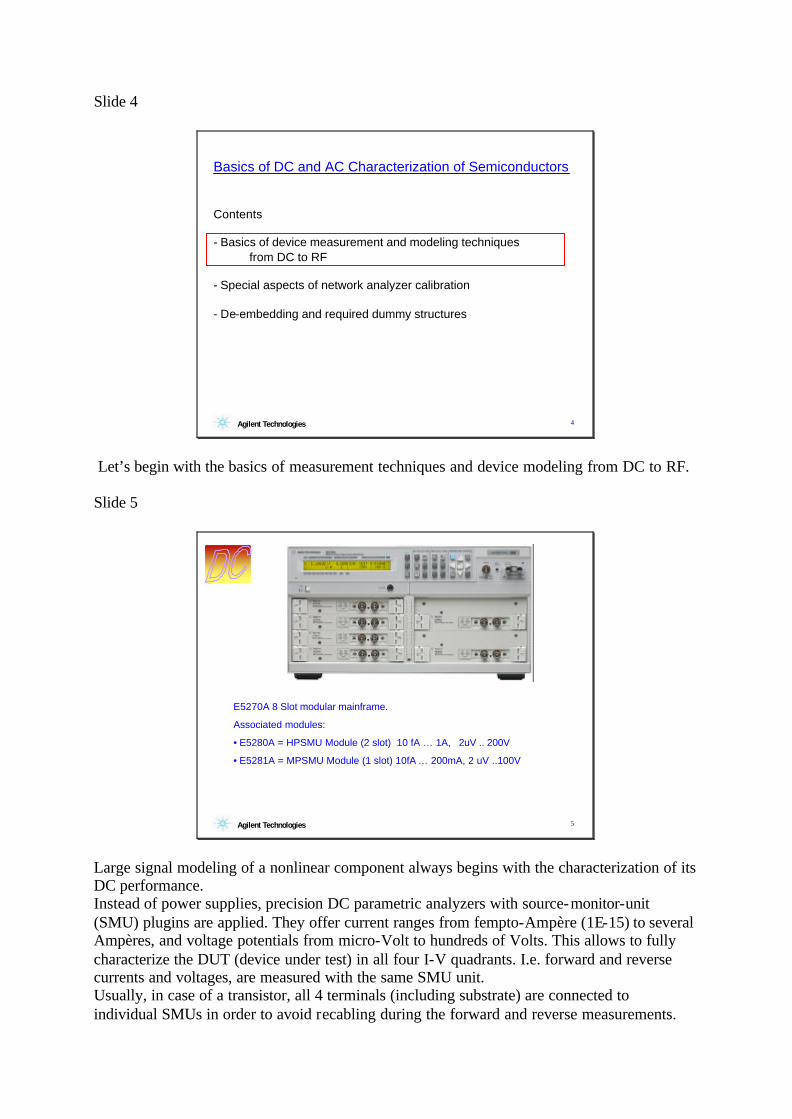
E5270A 8 Slot modular mainframe.
Associated modules:
• E5280A = HPSMU Module (2 slot) 10 fA … 1A, 2uV .. 200V
• E5281A = MPSMU Module (1 slot) 10fA … 200mA, 2 uV ..100V
Large signal modeling of a nonlinear component always begins with the characterization of its DC performance. Instead of power supplies, precision DC parametric analyzers with source-monitor-unit (SMU) plugins are applied. They offer current ranges from fempto-Ampère (1E-15) to several Ampères, and voltage potentials from micro-Volt to hundreds of Volts. This allows to fully characterize the DUT (device under test) in all four I-V quadrants. I.e. forward and reverse currents and voltages, are measured with the same SMU unit. Usually, in case of a transistor, all 4 terminals (including substrate) are connected to individual SMUs in order to avoid recabling during the forward and reverse measurements.
Slide 6
6Agilent Technologies
-
+
desiredvoltage
Force
Sense
Test Potential
Measurement Instrument
MeteringLines
SMU
OpAmp1
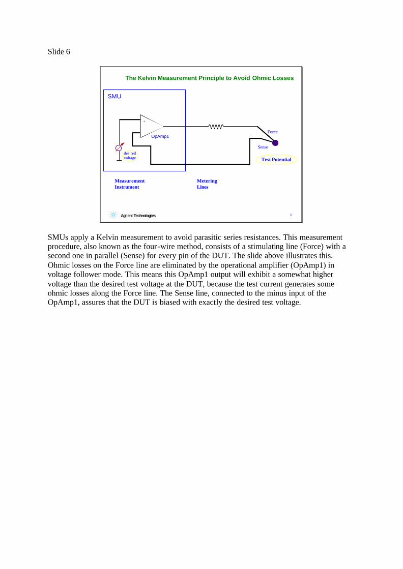
The Kelvin Measurement Principle to Avoid Ohmic Losses
SMUs apply a Kelvin measurement to avoid parasitic series resistances. This measurement procedure, also known as the four-wire method, consists of a stimulating line (Force) with a second one in parallel (Sense) for every pin of the DUT. The slide above illustrates this. Ohmic losses on the Force line are eliminated by the operational amplifier (OpAmp1) in voltage follower mode. This means this OpAmp1 output will exhibit a somewhat higher voltage than the desired test voltage at the DUT, because the test current generates some ohmic losses along the Force line. The Sense line, connected to the minus input of the OpAmp1, assures that the DUT is biased with exactly the desired test voltage.
Slide 7
7Agilent Technologies
-
+
desiredvoltage
Force
x 1
SenseDielectric Losses
Ohmic Losses
Test Potential
Inner Shielding
External Shielding
Measurement Instrument
MeteringLines
SMU
OpAmp1
OpAmp2
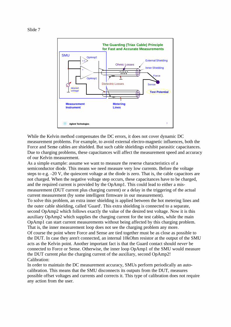
The Guarding (Triax Cable) Principle for Fast and Accurate Measurements
While the Kelvin method compensates the DC errors, it does not cover dynamic DC measurement problems. For example, to avoid external electro-magnetic influences, both the Force and Sense cables are shielded. But such cable shieldings exhibit parasitic capacitances. Due to charging problems, these capacitances will affect the measurement speed and accuracy of our Kelvin measurement. As a simple example: assume we want to measure the reverse characteristics of a semiconductor diode. This means we need measure very low currents. Before the voltage steps to e.g. -20 V, the quiescent voltage at the diode is zero. That is, the cable capacitors are not charged. When the negative voltage step occurs, these capacitances have to be charged, and the required current is provided by the OpAmp1. This could lead to either a mis-measurement (DUT current plus charging current) or a delay in the triggering of the actual current measurement (by some intelligent firmware in our measurement). To solve this problem, an extra inner shielding is applied between the hot metering lines and the outer cable shielding, called 'Guard'. This extra shielding is connected to a separate, second OpAmp2 which follows exactly the value of the desired test voltage. Now it is this auxiliary OpAmp2 which supplies the charging current for the test cables, while the main OpAmp1 can start current measurements without being affected by this charging problem. That is, the inner measurement loop does not see the charging problem any more. Of course the point where Force and Sense are tied together must be as close as possible to the DUT. In case they aren't connected, an internal 10kOhm resistor at the output of the SMU acts as the Kelvin point. Another important fact is that the Guard contact should never be connected to Force or Sense. Otherwise, the inner loop OpAmp1 of the SMU would measure the DUT current plus the charging current of the auxiliary, second OpAmp2! Calibration: In order to maintain the DC measurement accuracy, SMUs perform periodically an auto-calibration. This means that the SMU disconnects its outputs from the DUT, measures possible offset voltages and currents and corrects it. This type of calibration does not require any action from the user.
Slide 8
Agilent Technologies
Measurement Environment
Complete triaxial systemHP 4155/56 Patented MicroChamber™
DCP-150KSDCP-150KS
Chuck
Shield Layer
Force
SMU 1
Sense
SMU 2
SMU 3
SMU 4
Guard Layer
Chuck
Shield Layer
RF & Microwave Measurement Techniques, Methods and Troubleshooting
Innovating Test Technologies
for better measurements faster
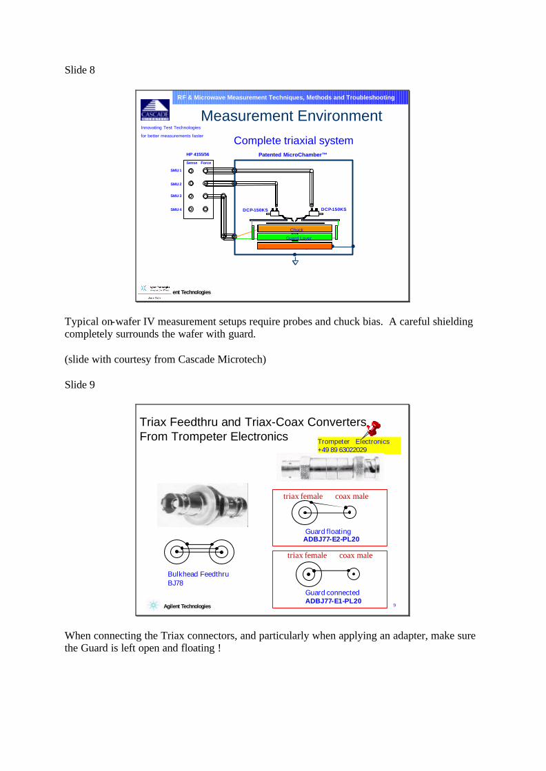
Typical on-wafer IV measurement setups require probes and chuck bias. A careful shielding completely surrounds the wafer with guard. (slide with courtesy from Cascade Microtech) Slide 9
9Agilent Technologies
Triax Feedthru and Triax-Coax ConvertersFrom Trompeter Electronics
Bulkhead FeedthruBJ78
Trompeter Electronics+49 89 63022029
ADBJ77-E2-PL20Guard floating
triax female coax male
Guard connected
triax female coax male
ADBJ77-E1-PL20
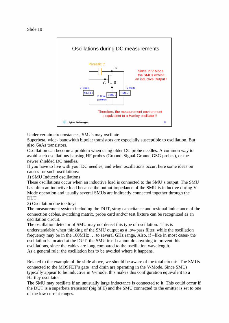
When connecting the Triax connectors, and particularly when applying an adapter, make sure the Guard is left open and floating !
Slide 10
10Agilent Technologies
Oscillations during DC measurements
Therefore, the measurement environment is equivalent to a Hartley oscillator !!
V Mode
SMU-1 SMU-2 SMU-3
Parasitic C
V Mode
V Mode(common)
G
D
S
Since in V Mode,the SMUs exhibit
an inductive Output !
Under certain circumstances, SMUs may oscillate. Superbeta, wide- bandwidth bipolar transistors are especially susceptible to oscillation. But also GaAs transistors. Oscillation can become a problem when using older DC probe needles. A common way to avoid such oscillations is using HF probes (Ground-Signal-Ground GSG probes), or the newer shielded DC needles. If you have to live with your DC needles, and when oscillations occur, here some ideas on causes for such oscillations: 1) SMU Induced oscillations These oscillations occur when an inductive load is connected to the SMU’s output. The SMU has often an inductive load because the output impedance of the SMU is inductive during V-Mode operation and usually several SMUs are indirectly connected together through the DUT. 2) Oscillation due to strays The measurement system including the DUT, stray capacitance and residual inductance of the connection cables, switching matrix, probe card and/or test fixture can be recognized as an oscillation circuit. The oscillation detector of SMU may not detect this type of oscillation. This is understandable when thinking of the SMU output as a low-pass filter, while the oscillation frequency may be in the 100MHz … to several GHz range. Also, if –like in most cases- the oscillation is located at the DUT, the SMU itself cannot do anything to prevent this oscillations, since the cables are long compared to the oscillation wavelength. As a general rule: the oscillation has to be avoided where it happens. Related to the example of the slide above, we should be aware of the total circuit: The SMUs connected to the MOSFET’s gate and drain are operating in the V-Mode. Since SMUs typically appear to be inductive in V-mode, this makes this configuration equivalent to a Hartley oscillator ! The SMU may oscillate if an unusually large inductance is connected to it. This could occur if the DUT is a superbeta transistor (big hFE) and the SMU connected to the emitter is set to one of the low current ranges.
For more details on conditions for oscillations, refer to the application note 356 -1 (publication number Agilent 5950-2954) Slide 11
11Agilent Technologies
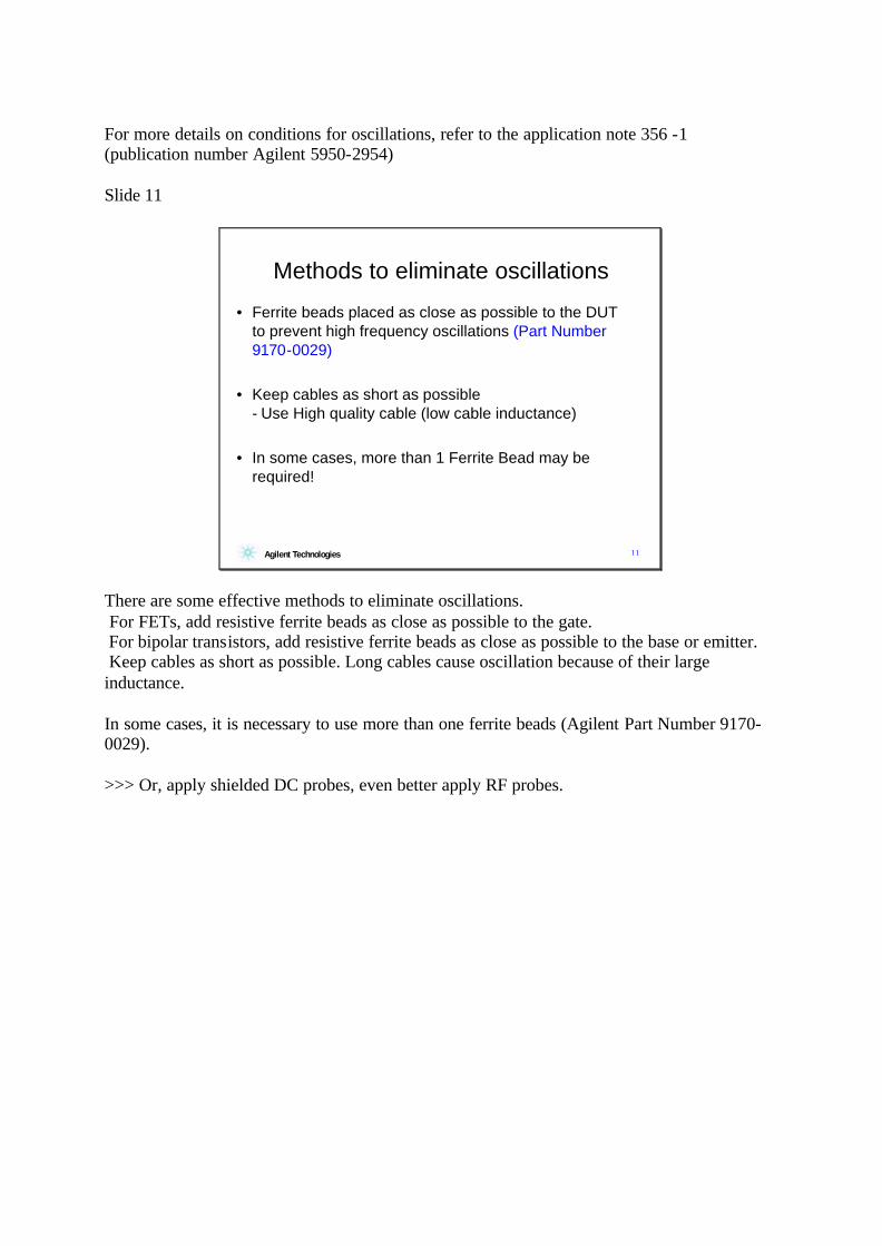
Methods to eliminate oscillations
• Ferrite beads placed as close as possible to the DUT to prevent high frequency oscillations (Part Number 9170-0029)
• Keep cables as short as possible - Use High quality cable (low cable inductance)
• In some cases, more than 1 Ferrite Bead may be required!
There are some effective methods to eliminate oscillations. For FETs, add resistive ferrite beads as close as possible to the gate. For bipolar transistors, add resistive ferrite beads as close as possible to the base or emitter. Keep cables as short as possible. Long cables cause oscillation because of their large inductance. In some cases, it is necessary to use more than one ferrite beads (Agilent Part Number 9170-0029). >>> Or, apply shielded DC probes, even better apply RF probes.
Slide 12
12Agilent Technologies
100 200 300 400
Tem
pera
ture
Ris
e (
'C)
Bias = 1 Watt
Time (µs)
20
40
60
80
Bias = 0.25 Watt
Bias = 0.50 Watt
Bias = 0.75 Watt
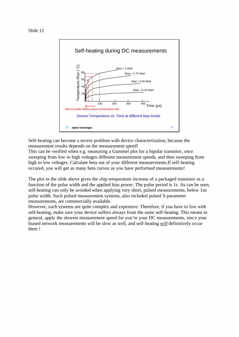
Device Temperature vs. Time at different bias levels
Narrow pulse widths reduce temperature rise
Self-heating during DC measurements
Self-heating can become a severe problem with device characterization, because the measurement results depends on the measurement speed! This can be verified when e.g. measuring a Gummel plot for a bipolar transistor, once sweeping from low to high voltages different measurement speeds, and then sweeping from high to low voltages. Calculate beta out of your different measurements.If self-heating occured, you will get as many beta curves as you have performed measurements! The plot in the slide above gives the chip temperature increase of a packaged transistor as a function of the pulse width and the applied bias power. The pulse period is 1s. As can be seen, self-heating can only be avoided when applying very short, pulsed measurements, below 1us pulse width. Such pulsed measurement systems, also included pulsed S-parameter measurements, are commercially available. However, such systems are quite complex and expensive. Therefore, if you have to live with self-heating, make sure your device suffers always from the same self-heating. This means in general, apply the slowest measurement speed for you’re your DC measurements, since your biased network measurements will be slow as well, and self-heating will definitively occur there !
Slide 13
13Agilent Technologies
Semiconductor CV Measurement
Lcur Lpot Hpot Hcur
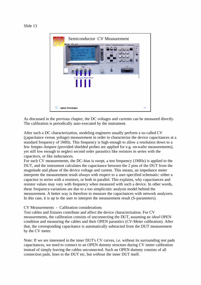
As discussed in the previous chapter, the DC voltages and currents can be measured directly. The calibration is periodically auto-executed by the instrument. After such a DC characterization, modeling engineers usually perform a so-called CV (capacitance versus voltage) measurement in order to characterize the device capacitances at a standard frequency of 1MHz. This frequency is high enough to allow a resolution down to a few fempto-Ampere (provided shielded probes are applied for e.g. on-wafer measurements), yet still low enough to neglect second order parasitics like resistors in series with the capacitors, or like inductances. For such CV measurements, the DC-bias is swept, a test frequency (1MHz) is applied to the DUT, and the instrument calculates the capacitance between the 2 pins of the DUT from the magnitude and phase of the device voltage and current. This means, an impedance meter interprete the measurement result always with respect to a user-specified schematic: either a capacitor in series with a resistors, or both in parallel. This explains, why capacitances and resistor values may vary with frequency when measured with such a device. In other words, these frequency-variations are due to a too simplicistic analysis model behind the measurement. A better way is therefore to measure the capacitances with network analyzers. In this case, it is up to the user to interpret the measurement result (S-parameters). CV Measurements - Calibration considerations Test cables and fixtures contribute and affect the device characterization. For CV measurements, the calibration consists of unconnecting the DUT, assuming an ideal OPEN condition and measuring the cables and their OPEN parasitics (CV-Meter calibration). After that, the corresponding capacitance is automatically subtracted from the DUT measurement by the CV meter. Note: If we are interested in the inner DUT's CV curves, i.e. without its surrounding test pads capacitances, we need to connect to an OPEN dummy structure during CV meter calibration instead of simply leaving the cables unconnected. Such an OPEN dummy consists of all connection pads, lines to the DUT etc, but without the inner DUT itself.
Slide 14
14Agilent Technologies
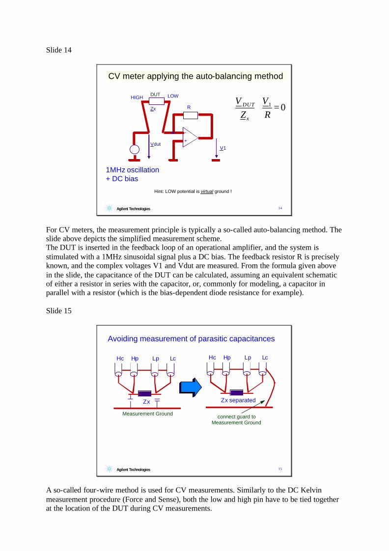
CV meter applying the auto-balancing method
1MHz oscillation+ DC bias
-
+
DUT
VdutV1
RZx
HIGH LOW
01 =+R
VZ
V
x
DUT
Hint: LOW potential is virtual ground !
For CV meters, the measurement principle is typically a so-called auto-balancing method. The slide above depicts the simplified measurement scheme. The DUT is inserted in the feedback loop of an operational amplifier, and the system is stimulated with a 1MHz sinusoidal signal plus a DC bias. The feedback resistor R is precisely known, and the complex voltages V1 and Vdut are measured. From the formula given above in the slide, the capacitance of the DUT can be calculated, assuming an equivalent schematic of either a resistor in series with the capacitor, or, commonly for modeling, a capacitor in parallel with a resistor (which is the bias-dependent diode resistance for example). Slide 15
15Agilent Technologies
Hc Hp Lp Lc
Zx
Hc Hp Lp Lc
Zx separated
connect guard to Measurement Ground
Measurement Ground
Avoiding measurement of parasitic capacitances
A so-called four-wire method is used for CV measurements. Similarly to the DC Kelvin measurement procedure (Force and Sense), both the low and high pin have to be tied together at the location of the DUT during CV measurements.
In the auto-balancing impedance measurement method, the shieldings of these four wires (which are not instrument chassis ground!) are connected to the virtual ground of the instrument's OpAmp. This eliminates any influences caused by the cables. Including this potential into the measurement setup allows the elimination of further stray capacitances. Like sketched above, it is possible to eliminate stray capacitances against ground (measurement plate). Slide 16
16Agilent Technologies
Shielded Measurementof CGD
S D
G CGD
With the auto-balancing method, connecting the Source to the cable shielding potential, isolates the effect of CGD, since both CGS and CDSare automatically excluded from the measurement result
Lcur Lpot Hpot Hcur
When characterizing the capacitances of transistors, the open 3rd transistor terminal should be connected to the shielding potential, eliminating the effect of the unwanted capacitors. Slide 17
17Agilent Technologies
AttoGuard™ Enhanced CV Measurements
• FemtoGuard surrounds the chuck at shield ground
• Patented AttoGuard above the chuck at shield ground
• Creates a virtual double-shielded Faraday enclosure
– 10 atto Farad CV measurement resolution
– Zero CV meter only one time
RF & Microwave Measurement Techniques, Methods and Troubleshooting
Innovating Test Technologies
for better measurements faster
The two shields insure equal potential everywhere inside the waferprober MicroChamber regardless of chuck locations. (slide with courtesy from Cascade Microtech)
Slide 18
18Agilent Technologies
Incident
Reflected Transmitted
R
BA
From Y-, Z-, and H-Parameters to S-Parameters
NOTE: on some elder NWAs,you can see the 3 RF cables for the Reflected signal, signal A and signal B !
Like Y-, Z-, H-Parameters, S-Parameters belong to linear circuit theory. This means, matrix conversions etc. Are only applicable
for linear operation of the device !
While the CV measurement is considered as a specific two-pin test condition, the situation changes for frequencies above 100MHz. The device is now operated under its originally intended environment conditions: DC bias is applied to all the pins, and an additional small-signal RF excitation is applied. Now, the sinusoidal currents and voltages at all pins of the DUT are to be measured, with magnitude and phase. A natural choice for such characterizations would be Z-, Y- or H-parameters from linear two-port theory. These two-port parameters can be used to completely describe the electrical behavior of our device (or network), including any source and load conditions. For such parameters, we have to measure the voltage or current as a function of frequency and bias at the ports of the device. At high frequencies, however, it is very hard to measure voltage and current at the device ports. One cannot simply connect a voltmeter or current probe and get accurate measurements due to the impedance of the probes themselves. Additionally, there is a difficulty to place the probes at the desired positions. Furthermore we have to apply either (AC-wise) OPEN or SHORT circuits as part of the Z-, Y- or H-parameter measurement. Active devices may oscillate or self-destruct with such terminations. To avoid these problems, twoports are described by S-parameters. IMPORTANT NOTE: like Y, Z, H parameters, S-Parameters are linear and belong to linear circuit theory. I.e. they represent the small-signal behavior of a device at a certain bias point, and for a certain frequency. Therefore, when measuring them, it must be assured that the linear device operation is maintained. As a consequence, linear S-parameters are independent of the applied RF signal power. Since twoport theory is restricted to linear circuit theory, matrix conversions (S to Y, S to Z etc. for de-embedding) are only applicable for linear operation of the device !
Slide 19
19Agilent Technologies
with| ai |2 power towards the two-port gate| bi |2 power away from the two-port gate
and| S11 |2 power reflected from port1| S12 |2 power transmitted from port1 to port2| S21 |2 power transmitted from port2 to port1| S22 |2 power reflected from port2
Definition of S-parametersReferring to the spectacles examples from above, i.e. power-wise, the S-parameters are defined as:
=
2
2
21
222
221
212
211
22
21 *
a
a
SS
SS
b
b
Slide 20
20Agilent Technologies
PowerDomain
|S11|2|a1|2
|b1|2
Z0 Z0
|a2|2
|b2|2
|S21|2|S12|2
|S22|2
0Zv*v
i*vP ==
Starting with normalized gives normalized amplitudespower to Z0 for voltage and current
00
Z*iZV
P ==
|a1| 2 VoltageDomain
a1
S-Parameters and Characteristic Impedance Z0
This means that S-parameters relate traveling waves (power) to a two-port's (DUT) reflection and transmission behavior. Since the two-port is imbedded in a characteristic impedance of Z0, and since we apply linear circuit theory (!), these 'waves' can be interpreted in terms of normalized voltage or current amplitudes. Note: think of the spectacles again: also here, the lens is imbedded on both sides with the same 'characteristic impedance', i.e. air !
Slide 21
21Agilent Technologies
a1
b1a2b2
S21S12
S11 S22
power
Z0
power
Z0port1 port2
Because of the characteristic impedance, we can convert the power towards the two-port into a normalized voltage amplitude of
and the power away from the two-port can be interpretedin terms of voltages like
0
_
Z
va twoporttowards
i =
0
__
Z
vb twoportfromaway
i =
Slide 22
22Agilent Technologies
a1
b1a2b2
S21S12
S11 S22
power
Z0
power
Z0port1 port2
02
1
2
1
221
=
==
avv
ab
Sporttowards
portofout
02
1
1
1
111
=
==
av
vab
Sporttowards
portatreflected
01
2
1
2
112
=
==
avv
abS
porttowards
portofout
01
2
2
2
222
=
==
av
v
ab
Sporttowards
portatreflected
Looking at the S-parameter coefficients individually, we have:
S11 and S21 are determined by measuring the magnitude and phase of the incident, reflected and transmitted signals when the output is terminated with a perfect Z0 load. This condition guarantees that a2 is zero. S11 is equivalent to the input complex reflection coefficient or impedance of the DUT, and S21 is the forward complex transmission coefficient. Likewise, by placing the source at port 2 and terminating port 1 in a perfect load (making a1 zero), S22 and S12 measurements can be made. S22 is equivalent to the output complex reflection coefficient or output impedance of the DUT, and S12 is the reverse complex transmission coefficient. The accuracy of S-parameter measurements depends greatly on how good a termination we apply to the port not being stimulated. Anything other than a perfect load will result in a1 or a2 not being zero (which violates the definition for S-parameters).
Slide 23
23Agilent Technologies
S11 and S22
value interpretation
-1 all voltage amplitudes towards the twoport are inverted and reflected (0 Ω)0 impedance matching, no reflections at all (50 Ω)
+1 voltage amplitudes are reflected (infinite Ω)
S21 and S12
magnitude interpretation
0 no signal transmission at all0 ... +1 input signal is damped in the Z0 environment
+1 unity gain signal transmission in the Z0 environment> +1 input signal is amplified in the Z0 environment
Interpreting S-parameters
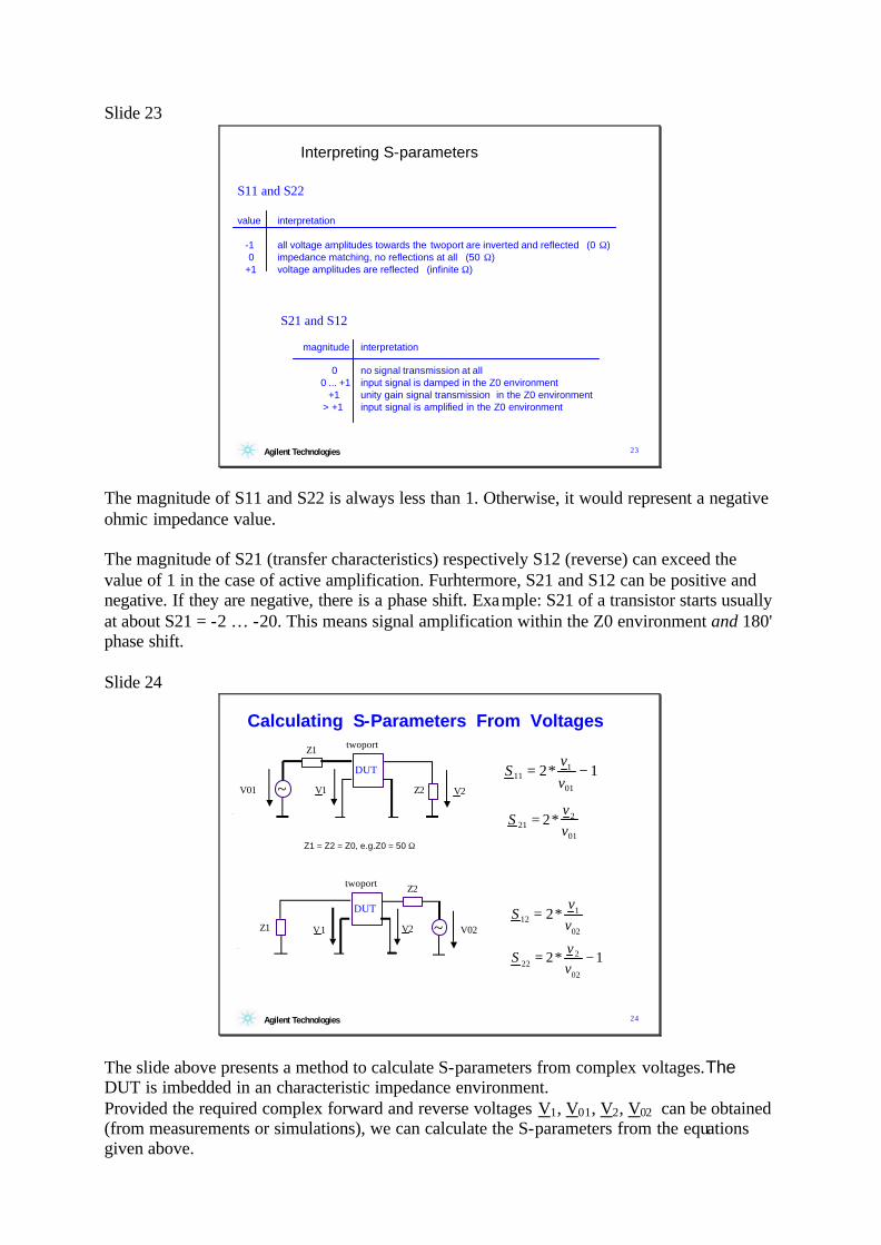
The magnitude of S11 and S22 is always less than 1. Otherwise, it would represent a negative ohmic impedance value. The magnitude of S21 (transfer characteristics) respectively S12 (reverse) can exceed the value of 1 in the case of active amplification. Furhtermore, S21 and S12 can be positive and negative. If they are negative, there is a phase shift. Example: S21 of a transistor starts usually at about S21 = -2 … -20. This means signal amplification within the Z0 environment and 180' phase shift. Slide 24
24Agilent Technologies
Z1
Z2V01 V1
twoport
~ V2
DUT
.
Z1 V1
twoport
V02~V2
DUT
Z2
.
Calculating S-Parameters From Voltages
1*201
111 −=
vv
S
01
221 *2
vv
S =
02
112 *2
vv
S =
1*202
222 −=
vv
S
Z1 = Z2 = Z0, e.g.Z0 = 50 Ω
The slide above presents a method to calculate S-parameters from complex voltages.The DUT is imbedded in an characteristic impedance environment. Provided the required complex forward and reverse voltages V1, V01, V2, V02 can be obtained (from measurements or simulations), we can calculate the S-parameters from the equations given above.
Slide 25
25Agilent Technologies
Understanding the Smith Chart
j50 Ω
50 Ω
R
1
4 3
2
-1 1
-j
j
1 2
3
4
R - Z0Γ = -----------
R + Z0
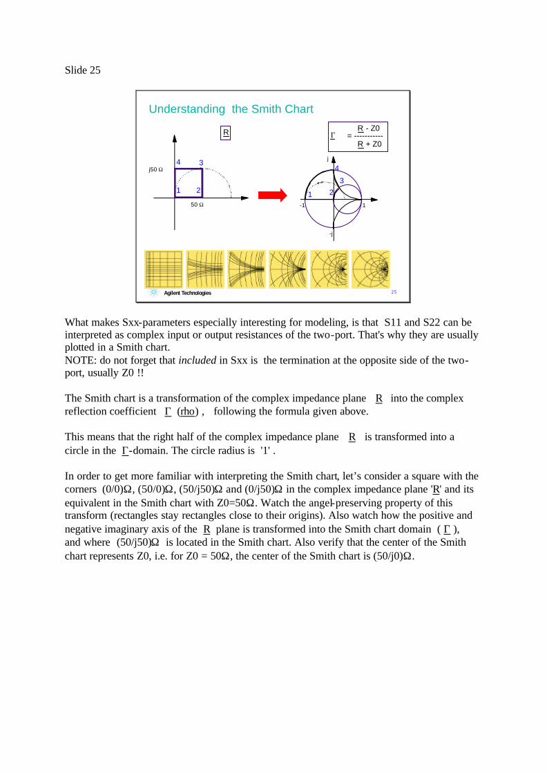
What makes Sxx-parameters especially interesting for modeling, is that S11 and S22 can be interpreted as complex input or output resistances of the two-port. That's why they are usually plotted in a Smith chart. NOTE: do not forget that included in Sxx is the termination at the opposite side of the two-port, usually Z0 !! The Smith chart is a transformation of the complex impedance plane R into the complex reflection coefficient Γ (rho) , following the formula given above. This means that the right half of the complex impedance plane R is transformed into a circle in the Γ-domain. The circle radius is '1' . In order to get more familiar with interpreting the Smith chart, let’s consider a square with the corners (0/0)Ω, (50/0)Ω, (50/j50)Ω and (0/j50)Ω in the complex impedance plane 'R' and its equivalent in the Smith chart with Z0=50Ω. Watch the angel-preserving property of this transform (rectangles stay rectangles close to their origins). Also watch how the positive and negative imaginary axis of the R plane is transformed into the Smith chart domain ( Γ ), and where (50/j50)Ω is located in the Smith chart. Also verify that the center of the Smith chart represents Z0, i.e. for Z0 = 50Ω, the center of the Smith chart is (50/j0)Ω.
Slide 26
26Agilent Technologies
1011
211 −⋅=vv
S
where v1 is the complex voltage at port 1 and v01 the stimulating AC source voltage (which is typically normalized to '1'). The corresponding circui t schematic is:
Z0
Z0V01
twoport
R
~~ V1
WHY A SMITH CHART FOR THE Sxx-PARAMETERS ??The voltage-related equation for the S11 parameter is
Under the assumption that R is the complex input resistance at port 1 and Z0 is the system impedance, we get applying the resistive divider formula for equation (1) from above:
00
10
211 ZRZR
ZRR
S+−
=−+
⋅=
And this is the reflection coefficient Γ from the Smith Chart definition !!
11
11
1
10
11
0S
SZZR
−
+⋅=
Γ−Γ+
⋅=Or, solved for the complex impedance R :
(1)
This explains how we can get the complex input/output resistance of a two-port directly from S11 or S22, if we plot these S-parameters in a Smith chart.
Slide 27
27Agilent Technologies
Interpreting S11 and S22 (Sxx)
jωL
1/jωC
R
inductive
capacitive
Z0
Z
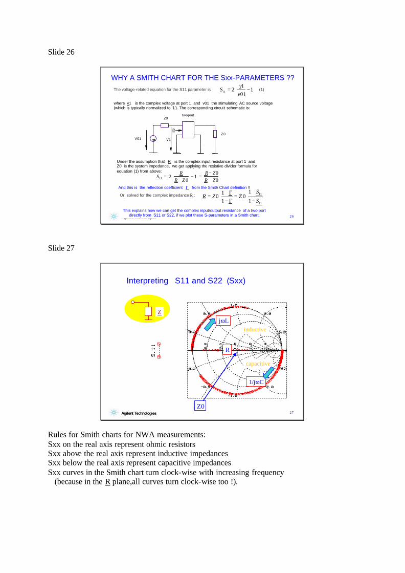
Rules for Smith charts for NWA measurements: Sxx on the real axis represent ohmic resistors Sxx above the real axis represent inductive impedances Sxx below the real axis represent capacitive impedances Sxx curves in the Smith chart turn clock-wise with increasing frequency (because in the R plane,all curves turn clock-wise too !).
Slide 28
28Agilent Technologies
f
iB
S11
Tutorial:S11 of a capacitor and of a bipolar transistor
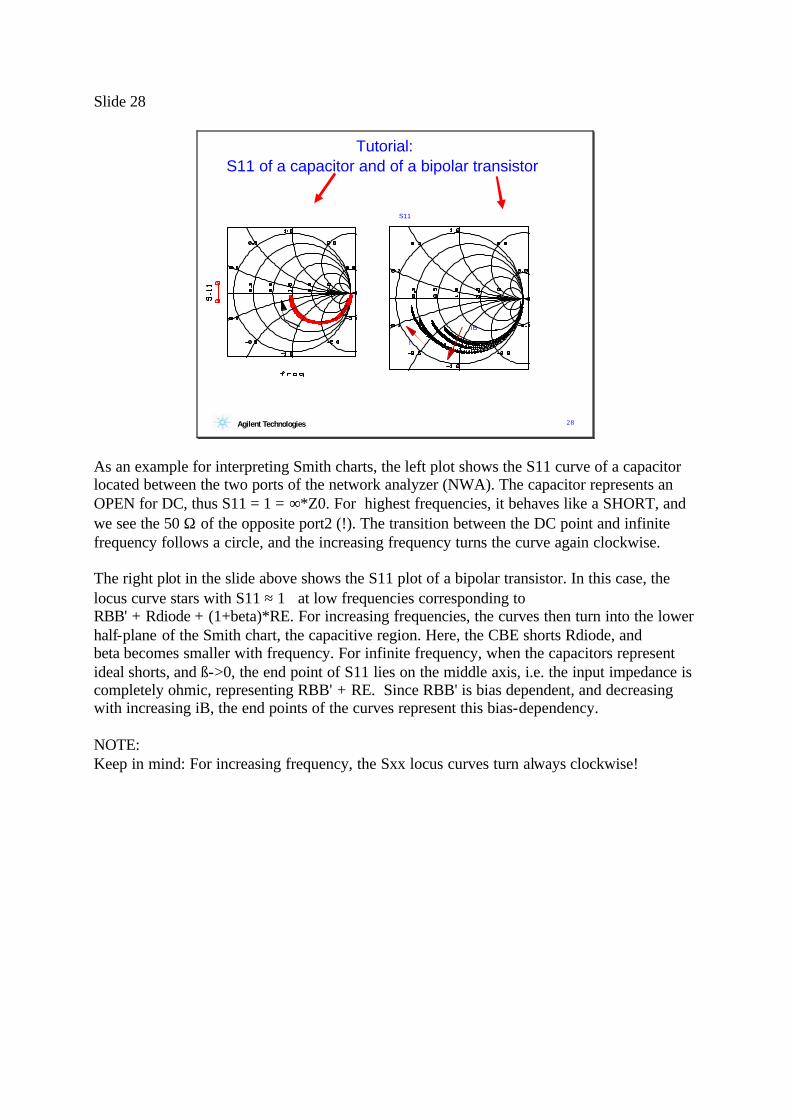
As an example for interpreting Smith charts, the left plot shows the S11 curve of a capacitor located between the two ports of the network analyzer (NWA). The capacitor represents an OPEN for DC, thus S11 = 1 = ∞*Z0. For highest frequencies, it behaves like a SHORT, and we see the 50 Ω of the opposite port2 (!). The transition between the DC point and infinite frequency follows a circle, and the increasing frequency turns the curve again clockwise. The right plot in the slide above shows the S11 plot of a bipolar transistor. In this case, the locus curve stars with S11 ≈ 1 at low frequencies corresponding to RBB' + Rdiode + (1+beta)*RE. For increasing frequencies, the curves then turn into the lower half-plane of the Smith chart, the capacitive region. Here, the CBE shorts Rdiode, and beta becomes smaller with frequency. For infinite frequency, when the capacitors represent ideal shorts, and ß->0, the end point of S11 lies on the middle axis, i.e. the input impedance is completely ohmic, representing RBB' + RE. Since RBB' is bias dependent, and decreasing with increasing iB, the end points of the curves represent this bias-dependency. NOTE: Keep in mind: For increasing frequency, the Sxx locus curves turn always clockwise!
Slide 29
29Agilent Technologies
1-1
j
-j
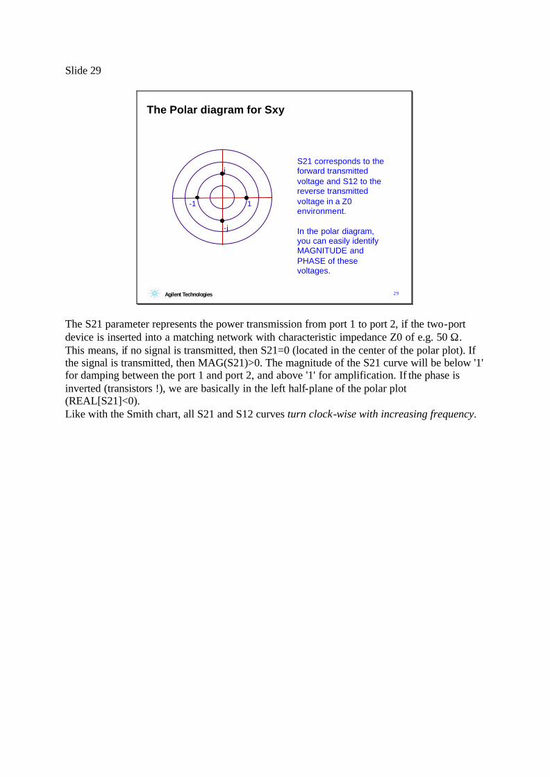
The Polar diagram for Sxy
S21 corresponds to the forward transmitted voltage and S12 to the reverse transmitted voltage in a Z0 environment.
In the polar diagram, you can easily identify MAGNITUDE and PHASE of these voltages.
The S21 parameter represents the power transmission from port 1 to port 2, if the two-port device is inserted into a matching network with characteristic impedance Z0 of e.g. 50 Ω. This means, if no signal is transmitted, then S21=0 (located in the center of the polar plot). If the signal is transmitted, then MAG(S21)>0. The magnitude of the S21 curve will be below '1' for damping between the port 1 and port 2, and above '1' for amplification. If the phase is inverted (transistors !), we are basically in the left half-plane of the polar plot (REAL[S21]<0). Like with the Smith chart, all S21 and S12 curves turn clock-wise with increasing frequency.
Slide 30
30Agilent Technologies
f
iB
f
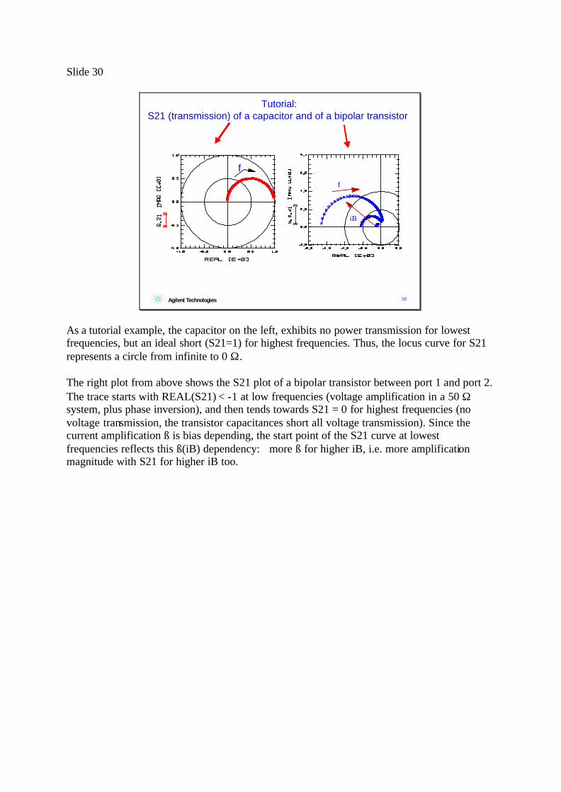
Tutorial:S21 (transmission) of a capacitor and of a bipolar transistor
As a tutorial example, the capacitor on the left, exhibits no power transmission for lowest frequencies, but an ideal short (S21=1) for highest frequencies. Thus, the locus curve for S21 represents a circle from infinite to 0 Ω. The right plot from above shows the S21 plot of a bipolar transistor between port 1 and port 2. The trace starts with REAL(S21) < -1 at low frequencies (voltage amplification in a 50 Ω system, plus phase inversion), and then tends towards S21 = 0 for highest frequencies (no voltage transmission, the transistor capacitances short all voltage transmission). Since the current amplification ß is bias depending, the start point of the S21 curve at lowest frequencies reflects this ß(iB) dependency: more ß for higher iB, i.e. more amplification magnitude with S21 for higher iB too.
Slide 31
31Agilent Technologies
Network Analyzer Mainframe
RF Synthesizer
S-Parameter Testset
test device DUT
hpibsignalflow
port1 port2
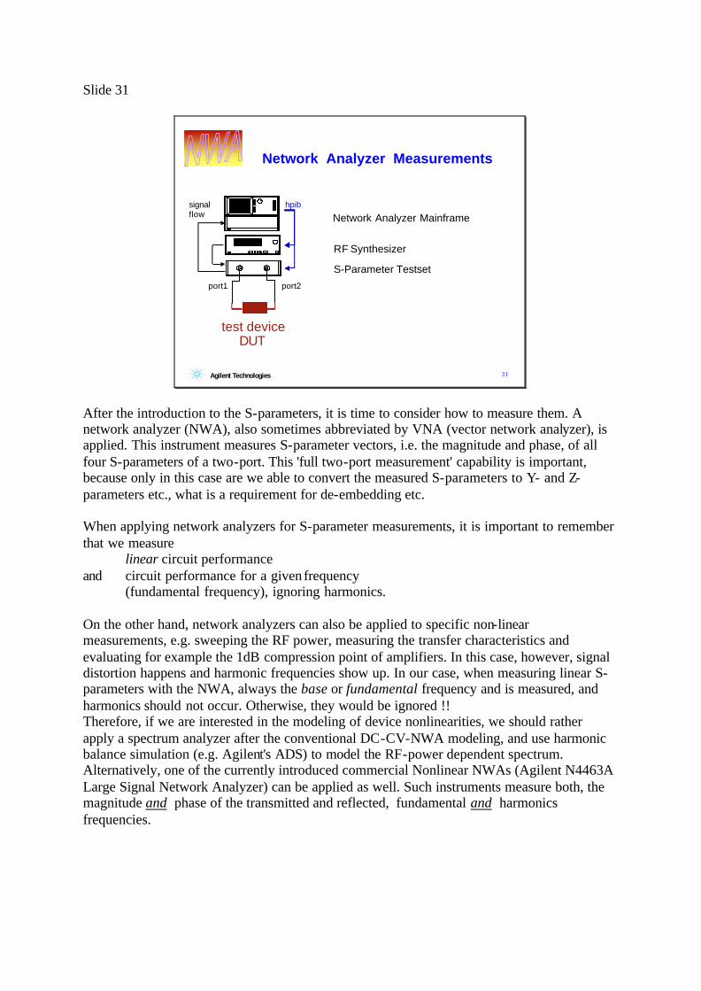
Network Analyzer Measurements
After the introduction to the S-parameters, it is time to consider how to measure them. A network analyzer (NWA), also sometimes abbreviated by VNA (vector network analyzer), is applied. This instrument measures S-parameter vectors, i.e. the magnitude and phase, of all four S-parameters of a two-port. This 'full two-port measurement' capability is important, because only in this case are we able to convert the measured S-parameters to Y- and Z-parameters etc., what is a requirement for de-embedding etc. When applying network analyzers for S-parameter measurements, it is important to remember that we measure linear circuit performance and circuit performance for a given frequency (fundamental frequency), ignoring harmonics. On the other hand, network analyzers can also be applied to specific non-linear measurements, e.g. sweeping the RF power, measuring the transfer characteristics and evaluating for example the 1dB compression point of amplifiers. In this case, however, signal distortion happens and harmonic frequencies show up. In our case, when measuring linear S-parameters with the NWA, always the base or fundamental frequency and is measured, and harmonics should not occur. Otherwise, they would be ignored !! Therefore, if we are interested in the modeling of device nonlinearities, we should rather apply a spectrum analyzer after the conventional DC-CV-NWA modeling, and use harmonic balance simulation (e.g. Agilent's ADS) to model the RF-power dependent spectrum. Alternatively, one of the currently introduced commercial Nonlinear NWAs (Agilent N4463A Large Signal Network Analyzer) can be applied as well. Such instruments measure both, the magnitude and phase of the transmitted and reflected, fundamental and harmonics frequencies.
Slide 32
32Agilent Technologies
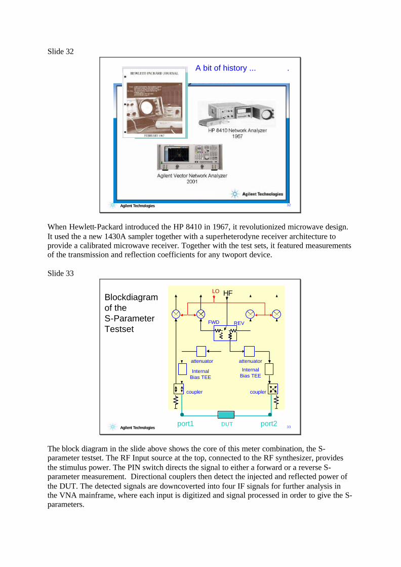
A bit of history ... .
When Hewlett-Packard introduced the HP 8410 in 1967, it revolutionized microwave design. It used the a new 1430A sampler together with a superheterodyne receiver architecture to provide a calibrated microwave receiver. Together with the test sets, it featured measurements of the transmission and reflection coefficients for any twoport device. Slide 33
33Agilent Technologies
Blockdiagram of theS-Parameter Testset
DUT
couplercoupler
port2port1
FWD REV
attenuator attenuator
InternalBias TEE
HFLO
InternalBias TEE
The block diagram in the slide above shows the core of this meter combination, the S-parameter testset. The RF Input source at the top, connected to the RF synthesizer, provides the stimulus power. The PIN switch directs the signal to either a forward or a reverse S-parameter measurement. Directional couplers then detect the injected and reflected power of the DUT. The detected signals are downcoverted into four IF signals for further analysis in the VNA mainframe, where each input is digitized and signal processed in order to give the S-parameters.
Slide 34
34Agilent Technologies
NWA measurements using the internal DC bias TEEs of the S-parameter testset
DCSource/Monitor
RF S-parameterTest Setwith internal bias TEEs
VectorNetworkAnalyzer
DUT
DC bias
controlsoftwareIC-CAP
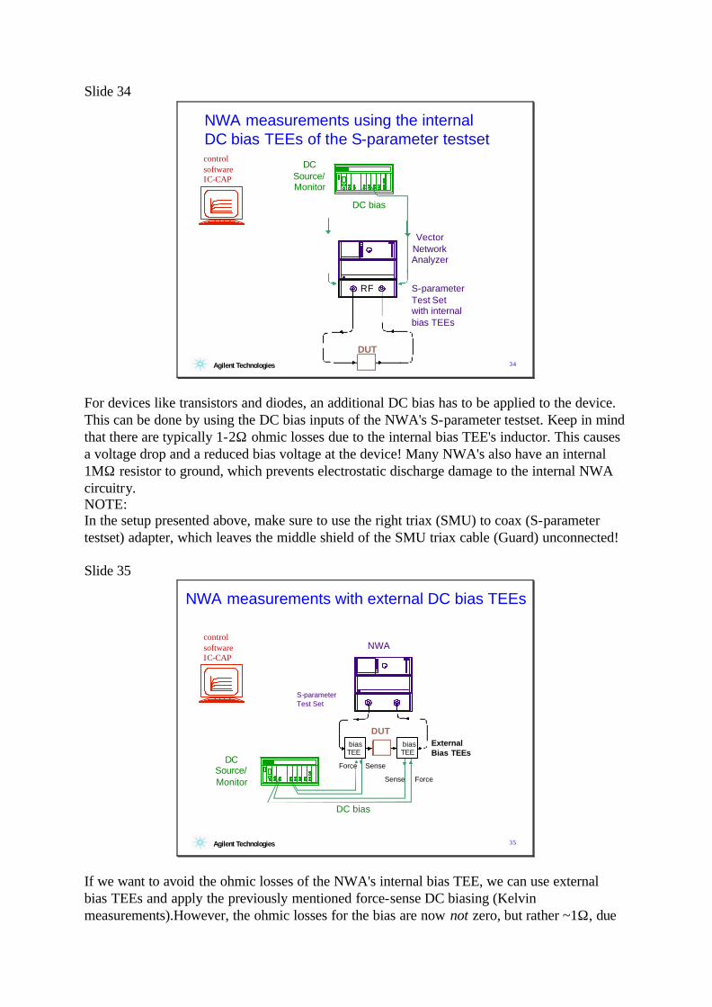
For devices like transistors and diodes, an additional DC bias has to be applied to the device. This can be done by using the DC bias inputs of the NWA's S-parameter testset. Keep in mind that there are typically 1-2Ω ohmic losses due to the internal bias TEE's inductor. This causes a voltage drop and a reduced bias voltage at the device! Many NWA's also have an internal 1MΩ resistor to ground, which prevents electrostatic discharge damage to the internal NWA circuitry. NOTE: In the setup presented above, make sure to use the right triax (SMU) to coax (S-parameter testset) adapter, which leaves the middle shield of the SMU triax cable (Guard) unconnected! Slide 35
35Agilent Technologies
NWA measurements with external DC bias TEEs
controlsoftwareIC-CAP
DUTExternalBias TEEs
biasTEE
Force Sense
DC bias
S-parameterTest Set
NWA
biasTEE
Sense Force
DCSource/Monitor
If we want to avoid the ohmic losses of the NWA's internal bias TEE, we can use external bias TEEs and apply the previously mentioned force-sense DC biasing (Kelvin measurements).However, the ohmic losses for the bias are now not zero, but rather ~1Ω, due
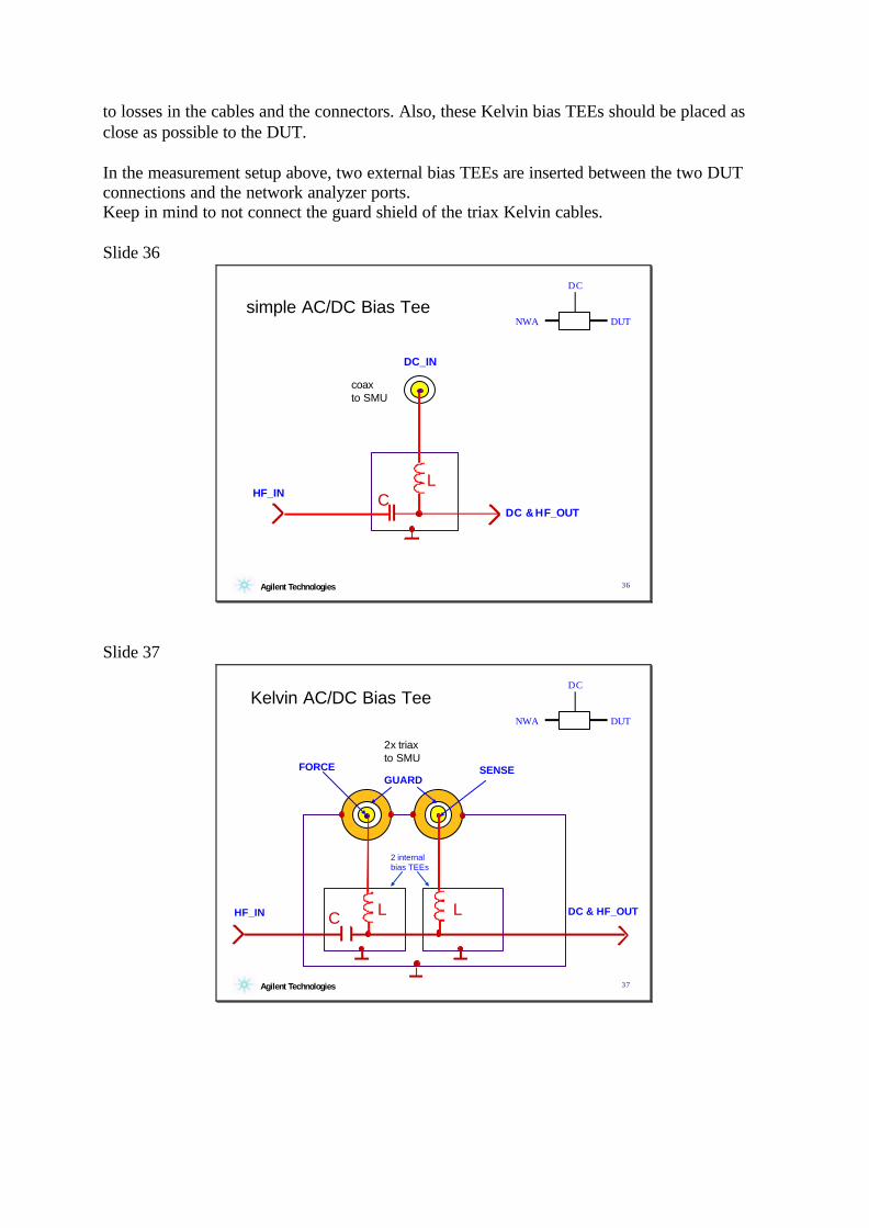
to losses in the cables and the connectors. Also, these Kelvin bias TEEs should be placed as close as possible to the DUT. In the measurement setup above, two external bias TEEs are inserted between the two DUT connections and the network analyzer ports. Keep in mind to not connect the guard shield of the triax Kelvin cables. Slide 36
36Agilent Technologies
simple AC/DC Bias Tee
HF_IN CL
coaxto SMU
DC & HF_OUT
DC_IN
DC
NWA DUT
Slide 37
37Agilent Technologies
DC
NWA DUT
Kelvin AC/DC Bias Tee
FORCE SENSE
HF_IN DC & HF_OUT
2 internal bias TEEs
C L L
2x triaxto SMU
GUARD
Slide 38
38Agilent Technologies
Basics of DC and AC Characterization of Semiconductors
Contents
- Basics of device measurement and modeling techniques from DC to RF
- Special aspects of network analyzer calibration
- De-embedding and required dummy structures
Slide 39
39Agilent Technologies
Vector Error Correction
accounts for all major sources of systematic error
S11 Measured
error vectors
S11 Device
S11Correction
Since S-parameters are vectors, all measurement errors contribute with magnitude and phase, and can be considered as additional error vectors. These errors have to be calibrated out with the correction vector Sxxcorrection, as depicted above.
Slide 40
40Agilent Technologies
12-Term error model of NWAs
directivity~AC
source
powersplitter
DUT
R
powercoupler
BAreference
crosstalk
sourcemissmatch
loadmismatch
frequency response:
reflection tracking (A/R)transmission tracking (B/R)
H(f)
f
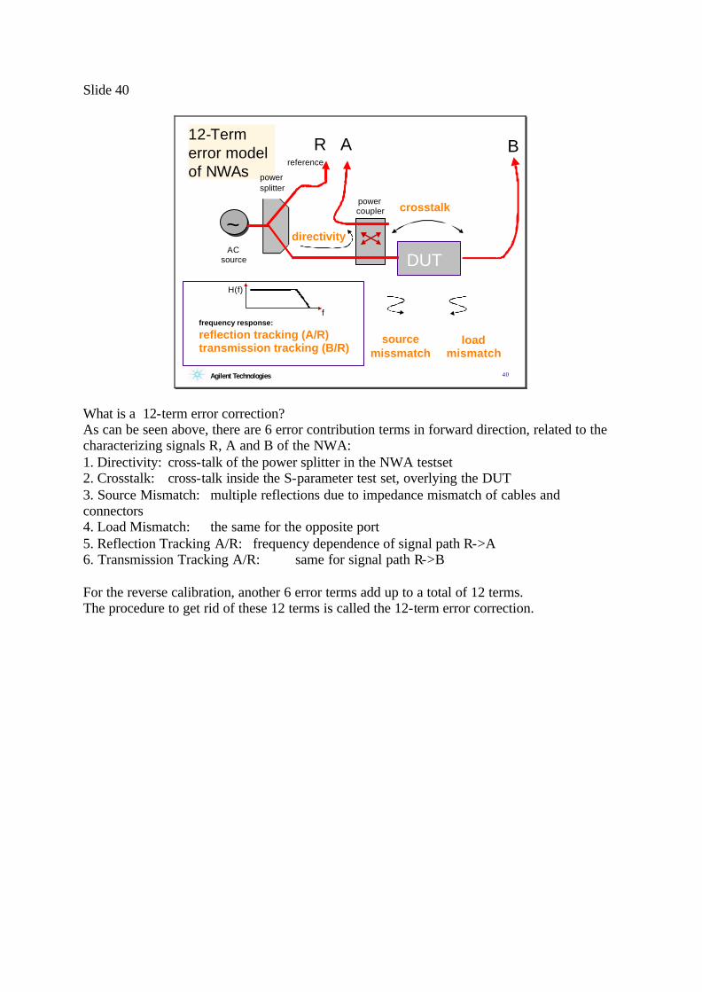
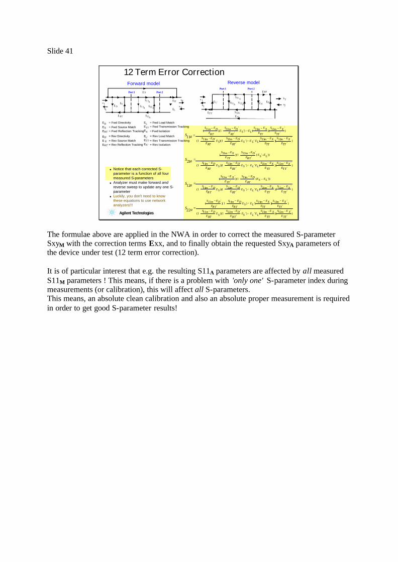
What is a 12-term error correction? As can be seen above, there are 6 error contribution terms in forward direction, related to the characterizing signals R, A and B of the NWA: 1. Directivity: cross-talk of the power splitter in the NWA testset 2. Crosstalk: cross-talk inside the S-parameter test set, overlying the DUT 3. Source Mismatch: multiple reflections due to impedance mismatch of cables and connectors 4. Load Mismatch: the same for the opposite port 5. Reflection Tracking A/R: frequency dependence of signal path R->A 6. Transmission Tracking A/R: same for signal path R->B For the reverse calibration, another 6 error terms add up to a total of 12 terms. The procedure to get rid of these 12 terms is called the 12-term error correction.
Slide 41
41Agilent Technologies
l Notice that each corrected S-parameter is a function of all four measured S-parameters
l Analyzer must make forward andreverse sweep to update any one S-parameter
l Luckily, you don't need to know these equations to use network analyzers!!!
12 Term Error Correction
= Fwd Directivity= Fwd Source Match= Fwd Reflection Tracking
= Fwd Load Match= Fwd Transmission Tracking= Fwd Isolation
ES
ED
ERT
ETT
EL
EX
= Rev Reflection Tracking= Rev Transmission Tracking
= Rev Directivity= Rev Source Match
= Rev Load Match
= Rev IsolationE S'
ED'
ERT'
ETT'
EL'
EX '
Port 1 Port 2E
S1 1
S2 1
S12
S22
ESE D
E RT
ETT
EL
a 1
b1
A
A
A
A
X
a 2
b2
Forward modelPort 1 Port 2
S11
S
S12
S 22 E S'ED '
E RT'
ETT'
E L'a 1
b1A
A
A
E X'
21 A
a2
b2
Reverse model
S a
S m EDERT
S m EDERT
ES ELS m EX
ETT
S m EXETT
S m ED'ERT
ESS m ED
ERTES E L EL
S m EXETT
S m EXETT
11
11 1 22 21 12
1 11 1 22 21 12=
−+
−−
− −
+−
+−
−− −
( )('
'') ( )(
'
')
( )('
'' ) ' ( )(
'
')
S a
S m EXETT
S m EDERT
ES EL
S m EDERT
ESS m ED
ERTES EL
21
21 22
1 11 1 22=
−1+
−−
+−
+−
−
( )('
'( ' ))
( )('
'' ) ' ( )(
'
')EL
S m EXETT
S m EXETT
21 12− −
'S E S E− −(
')( ( '))
( )('
'' ) ' ( )(
'
')
m XETT
m DERT
ES EL
S m EDERT
ESS m ED
ERTES EL EL
S m EXETT
S m EXETT
S a
12 1 11
1 11 1 22 21 1212
+ −
+−
+−
−− −
=
('
')(
(
S m EDERT
S m EDERT
S a
22
1 1122
−) '( )(
'
')
S m EDERT
ES ELS m EX
ETT
S m EXETT
11 21 12−−
− −
+−
=ES
S m EDERT
ES EL ELS m E X
ETT
S m E XETT
)('
'' ) ' ( )(
'
')1 22 21 12
+−
−− −
1+
The formulae above are applied in the NWA in order to correct the measured S-parameter SxyM with the correction terms Exx, and to finally obtain the requested SxyA parameters of the device under test (12 term error correction). It is of particular interest that e.g. the resulting S11A parameters are affected by all measured S11M parameters ! This means, if there is a problem with 'only one' S-parameter index during measurements (or calibration), this will affect all S-parameters. This means, an absolute clean calibration and also an absolute proper measurement is required in order to get good S-parameter results!
Slide 42
42Agilent Technologies
Calibrating a NWA
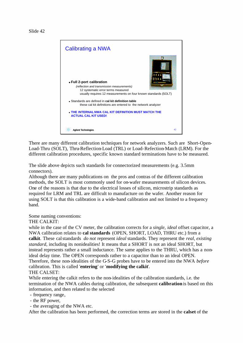
l Full 2-port calibration(reflection and transmission measurements)
12 systematic error terms measuredusually requires 12 measurements on four known standards (SOLT)
l Standards are defined in cal kit definition tablethese cal kit definitions are entered to the network analyzer
l THE INTERNAL NWA CAL KIT DEFINITION MUST MATCH THE ACTUAL CAL KIT USED!
There are many different calibration techniques for network analyzers. Such are Short-Open-Load-Thru (SOLT), Thru-Reflection-Load (TRL) or Load-Refection-Match (LRM). For the different calibration procedures, specific known standard terminations have to be measured. The slide above depicts such standards for connectorized measurements (e.g. 3.5mm connectors). Although there are many publications on the pros and contras of the different calibration methods, the SOLT is most commonly used for on-wafer measurements of silicon devices. One of the reasons is that due to the electrical losses of silicon, microstrip standards as required for LRM and TRL are difficult to manufacture on the wafer. Another reason for using SOLT is that this calibration is a wide-band calibration and not limited to a frequency band. Some naming conventions: THE CALKIT: while in the case of the CV meter, the calibration corrects for a single, ideal offset capacitor, a NWA calibration relates to cal standards (OPEN, SHORT, LOAD, THRU etc.) from a calkit. These cal standards do not represent ideal standards. They represent the real, existing standard, including its nonidealities! It means that a SHORT is not an ideal SHORT, but instead represents rather a small inductance. The same applies to the THRU, which has a non-ideal delay time. The OPEN corresponds rather to a capacitor than to an ideal OPEN. Therefore, these non- idealities of the G-S-G probes have to be entered into the NWA before calibration. This is called 'entering ' or 'modifying the calkit'. THE CALSET: While entering the calkit refers to the non- idealities of the calibration standards, i.e. the termination of the NWA cables during calibration, the subsequent calibration is based on this information, and then related to the selected - frequency range, - the RF power, - the averaging of the NWA etc. After the calibration has been performed, the correction terms are stored in the calset of the
NWA. In other words, the 12-term error vectors are 'filled up', and can be used with the measurements afterwards. Finally, when the measurements are performed, the raw measured data arrays will be corrected inside the NWA, using a correction technique related to the selected calibration method, and referring to the specified calset. When using a NWA driver software, this corrected measurement result is transferred into the software and displayed there. NOTE: After the calibration, a re-measurement of the OPEN will not represent an ideal open, but instead exactly those parasitic components as described in the documentation of the OPEN. In the same way, a THRU shows up after calibration with its real delay time, and a SHORT represents its inductive behavior! If the calibration was ok, the remeasured standards should give exactly the same parameter values as previously entered into the NWA calkit. Slide 43
43Agilent Technologies
SOLT calibration for on-waferGround-Signal-Ground probes(G_S_G)
50 Ω LOADOPEN
SHORT THRU
Probes in the air
SOLTcalibration
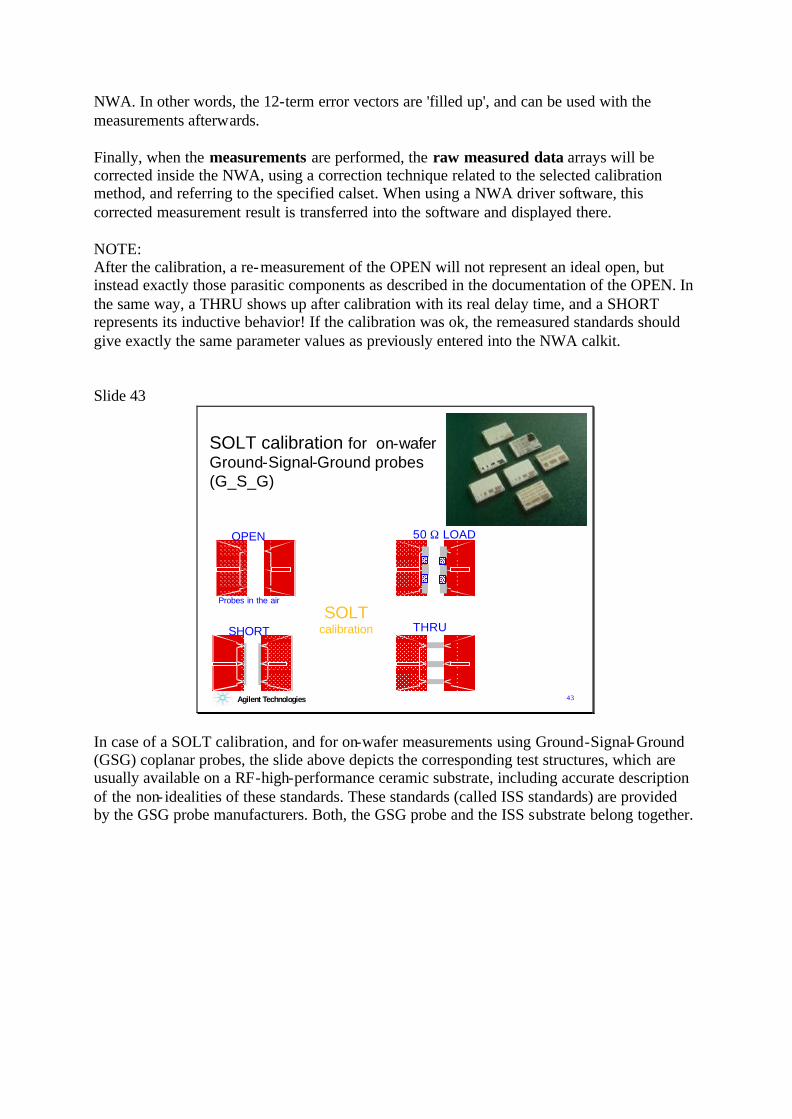
In case of a SOLT calibration, and for on-wafer measurements using Ground-Signal-Ground (GSG) coplanar probes, the slide above depicts the corresponding test structures, which are usually available on a RF-high-performance ceramic substrate, including accurate description of the non- idealities of these standards. These standards (called ISS standards) are provided by the GSG probe manufacturers. Both, the GSG probe and the ISS substrate belong together.
Slide 44
44Agilent Technologies
Extending linear to RF power dependent signals
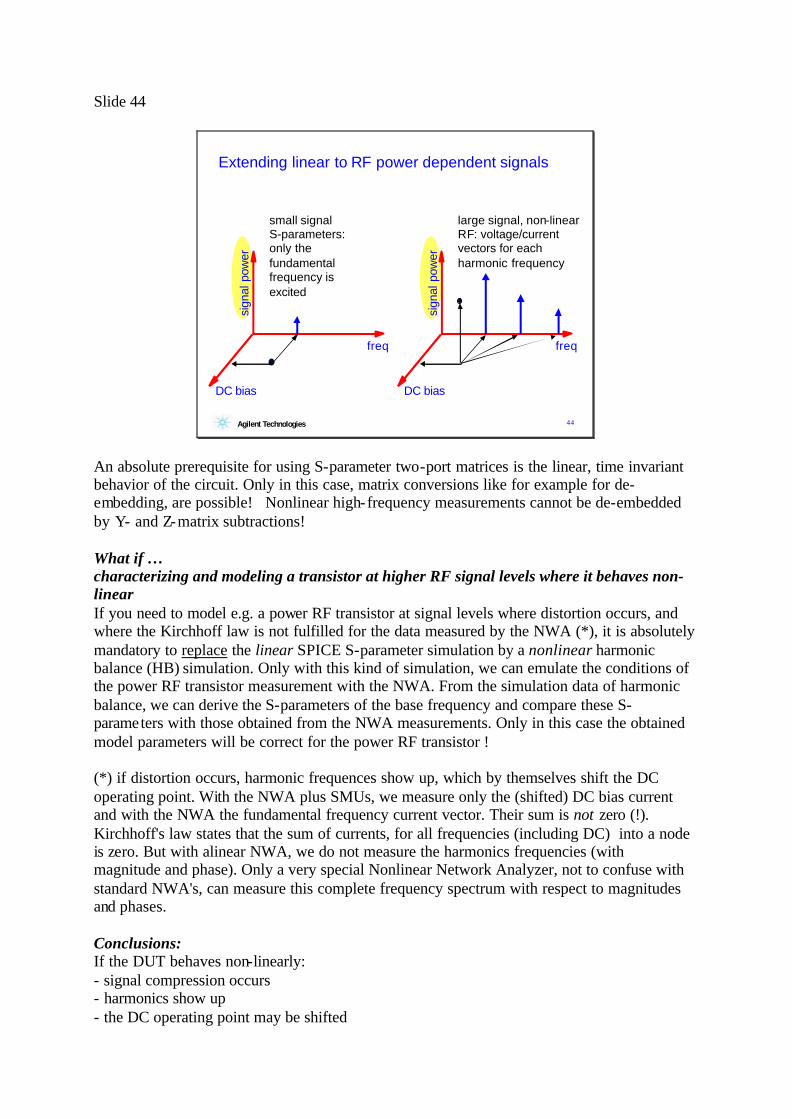
small signalS-parameters: only the fundamental frequency is excited
freq
DC bias
sign
al p
ower
large signal, non-linear RF: voltage/current vectors for each harmonic frequency
freq
DC bias
sign
al p
ower
An absolute prerequisite for using S-parameter two-port matrices is the linear, time invariant behavior of the circuit. Only in this case, matrix conversions like for example for de-embedding, are possible! Nonlinear high-frequency measurements cannot be de-embedded by Y- and Z-matrix subtractions! What if … characterizing and modeling a transistor at higher RF signal levels where it behaves non-linear If you need to model e.g. a power RF transistor at signal levels where distortion occurs, and where the Kirchhoff law is not fulfilled for the data measured by the NWA (*), it is absolutely mandatory to replace the linear SPICE S-parameter simulation by a nonlinear harmonic balance (HB) simulation. Only with this kind of simulation, we can emulate the conditions of the power RF transistor measurement with the NWA. From the simulation data of harmonic balance, we can derive the S-parameters of the base frequency and compare these S-parameters with those obtained from the NWA measurements. Only in this case the obtained model parameters will be correct for the power RF transistor ! (*) if distortion occurs, harmonic frequences show up, which by themselves shift the DC operating point. With the NWA plus SMUs, we measure only the (shifted) DC bias current and with the NWA the fundamental frequency current vector. Their sum is not zero (!). Kirchhoff's law states that the sum of currents, for all frequencies (including DC) into a node is zero. But with alinear NWA, we do not measure the harmonics frequencies (with magnitude and phase). Only a very special Nonlinear Network Analyzer, not to confuse with standard NWA's, can measure this complete frequency spectrum with respect to magnitudes and phases. Conclusions: If the DUT behaves non-linearly: - signal compression occurs - harmonics show up - the DC operating point may be shifted
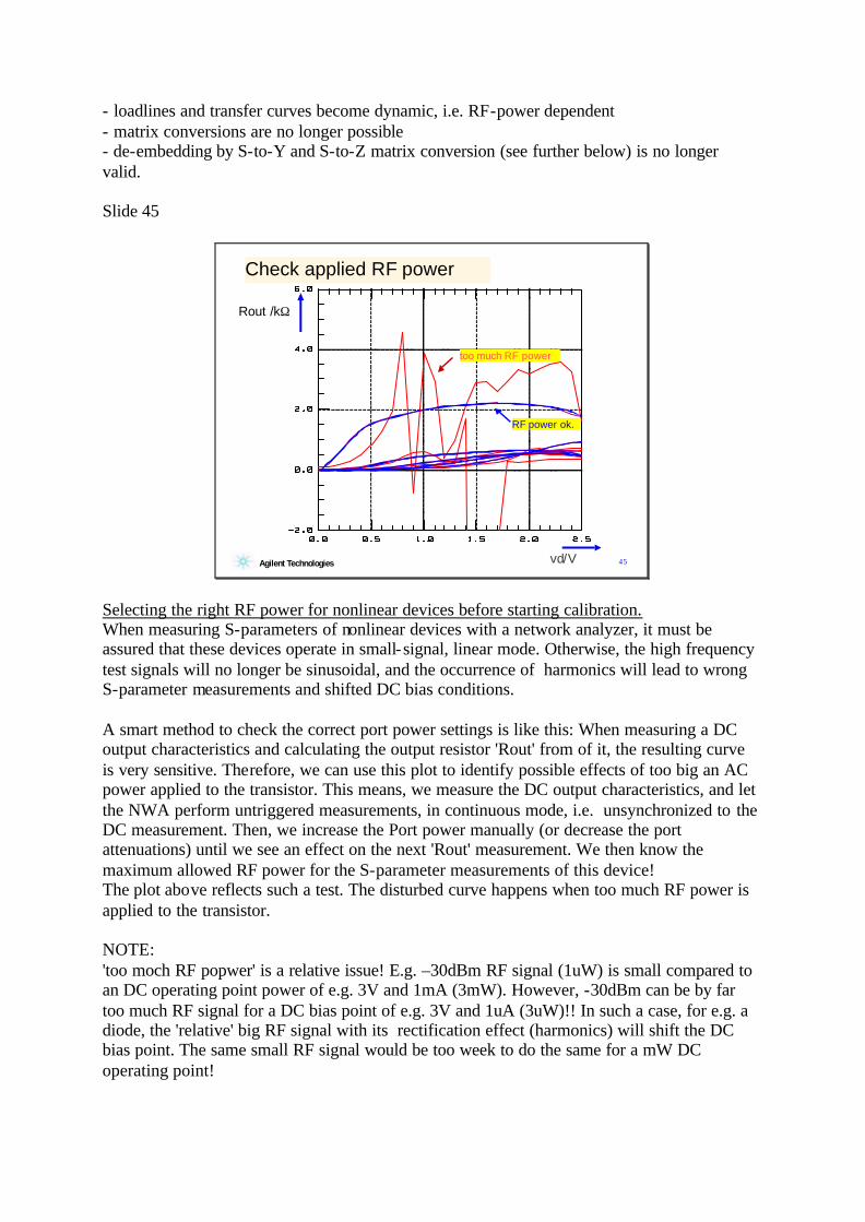
- loadlines and transfer curves become dynamic, i.e. RF-power dependent - matrix conversions are no longer possible - de-embedding by S-to-Y and S-to-Z matrix conversion (see further below) is no longer valid. Slide 45
45Agilent Technologies
Check applied RF power
RF power ok.
too much RF power
Rout /kΩ
vd/V
Selecting the right RF power for nonlinear devices before starting calibration. When measuring S-parameters of nonlinear devices with a network analyzer, it must be assured that these devices operate in small-signal, linear mode. Otherwise, the high frequency test signals will no longer be sinusoidal, and the occurrence of harmonics will lead to wrong S-parameter measurements and shifted DC bias conditions. A smart method to check the correct port power settings is like this: When measuring a DC output characteristics and calculating the output resistor 'Rout' from of it, the resulting curve is very sensitive. Therefore, we can use this plot to identify possible effects of too big an AC power applied to the transistor. This means, we measure the DC output characteristics, and let the NWA perform untriggered measurements, in continuous mode, i.e. unsynchronized to the DC measurement. Then, we increase the Port power manually (or decrease the port attenuations) until we see an effect on the next 'Rout' measurement. We then know the maximum allowed RF power for the S-parameter measurements of this device! The plot above reflects such a test. The disturbed curve happens when too much RF power is applied to the transistor. NOTE: 'too moch RF popwer' is a relative issue! E.g. –30dBm RF signal (1uW) is small compared to an DC operating point power of e.g. 3V and 1mA (3mW). However, -30dBm can be by far too much RF signal for a DC bias point of e.g. 3V and 1uA (3uW)!! In such a case, for e.g. a diode, the 'relative' big RF signal with its rectification effect (harmonics) will shift the DC bias point. The same small RF signal would be too week to do the same for a mW DC operating point!
Slide 46
46Agilent Technologies
Verifying the NWA calibration
THRU
OPEN SHORT
-9.3fF
LOAD
1psec
2.4pH
50Ω
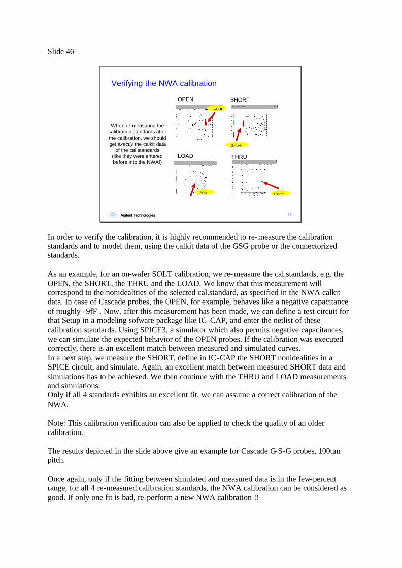
When re-measuring the calibration standards after the calibration, we should get exactly the calkit data
of the cal.standards (like they were entered before into the NWA!)
In order to verify the calibration, it is highly recommended to re-measure the calibration standards and to model them, using the calkit data of the GSG probe or the connectorized standards. As an example, for an on-wafer SOLT calibration, we re-measure the cal.standards, e.g. the OPEN, the SHORT, the THRU and the LOAD. We know that this measurement will correspond to the nonidealities of the selected cal.standard, as specified in the NWA calkit data. In case of Cascade probes, the OPEN, for example, behaves like a negative capacitance of roughly -9fF . Now, after this measurement has been made, we can define a test circuit for that Setup in a modeling sofware package like IC-CAP, and enter the netlist of these calibration standards. Using SPICE3, a simulator which also permits negative capacitances, we can simulate the expected behavior of the OPEN probes. If the calibration was executed correctly, there is an excellent match between measured and simulated curves. In a next step, we measure the SHORT, define in IC-CAP the SHORT nonidealities in a SPICE circuit, and simulate. Again, an excellent match between measured SHORT data and simulations has to be achieved. We then continue with the THRU and LOAD measurements and simulations. Only if all 4 standards exhibits an excellent fit, we can assume a correct calibration of the NWA. Note: This calibration verification can also be applied to check the quality of an older calibration. The results depicted in the slide above give an example for Cascade G-S-G probes, 100um pitch. Once again, only if the fitting between simulated and measured data is in the few-percent range, for all 4 re-measured calib ration standards, the NWA calibration can be considered as good. If only one fit is bad, re-perform a new NWA calibration !!
Slide 47
47Agilent Technologies
Basics of DC and AC Characterization of Semiconductors
Contents
- Basics of device measurement and modeling techniques from DC to RF
- Special aspects of network analyzer calibration
- De-embedding and required dummy structures
Slide 48
48Agilent Technologies
How parasitics degrade the device performance ...
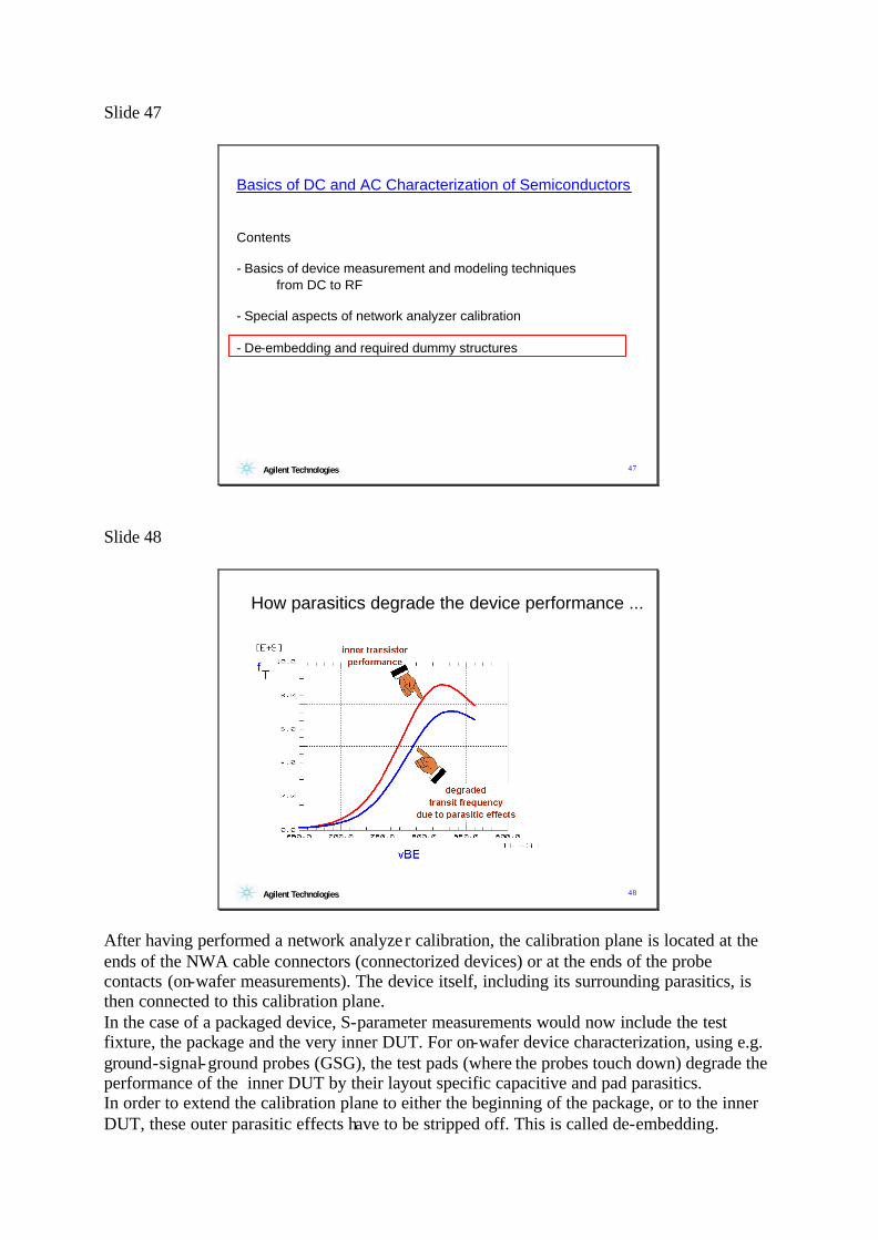
After having performed a network analyze r calibration, the calibration plane is located at the ends of the NWA cable connectors (connectorized devices) or at the ends of the probe contacts (on-wafer measurements). The device itself, including its surrounding parasitics, is then connected to this calibration plane. In the case of a packaged device, S-parameter measurements would now include the test fixture, the package and the very inner DUT. For on-wafer device characterization, using e.g. ground-signal-ground probes (GSG), the test pads (where the probes touch down) degrade the performance of the inner DUT by their layout specific capacitive and pad parasitics. In order to extend the calibration plane to either the beginning of the package, or to the inner DUT, these outer parasitic effects have to be stripped off. This is called de-embedding.
In the slide above, a brief example on how de-embedding returns the real, inner DUT performance without its degradation due to the measurement environment is given. We can clearly see how the transistor cutoff frequency fT is degraded due to these parasitics. Slide 49
49Agilent Technologies
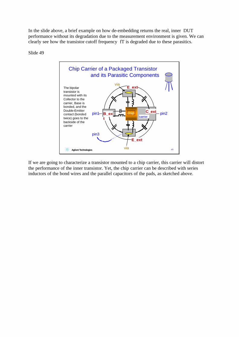
The bipolar transistor is mounted with its Collector to the carrier, Base is bonded, and theDouble-Emitter contact (bonded twice) goes to the backside of the carrier
Chip Carrier of a Packaged Transistor and its Parasitic Components
B C
E
E
B_ext
C_ext
E_ext
E_ext
pin1 pin2
pin3
via
chipcarrier
via
If we are going to characterize a transistor mounted to a chip carrier, this carrier will distort the performance of the inner transistor. Yet, the chip carrier can be described with series inductors of the bond wires and the parallel capacitors of the pads, as sketched above.
Slide 50
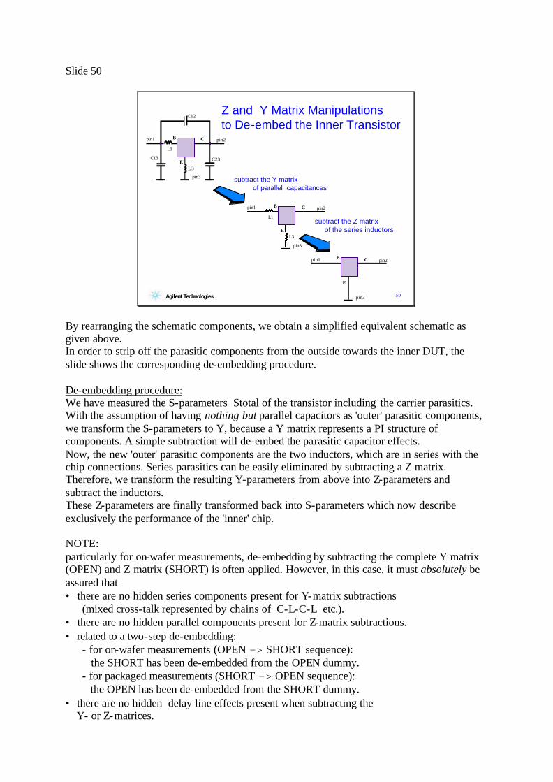
50Agilent Technologies
Z and Y Matrix Manipulations to De-embed the Inner Transistor
B C
E
pin1 pin2
pin3
pin2B C
E
pin1
pin3
C13 C23
C12
L1
L3
pin2B C
E
pin1
pin3
L1
L3
subtract the Y matrix of parallel capacitances
subtract the Z matrix of the series inductors
By rearranging the schematic components, we obtain a simplified equivalent schematic as given above. In order to strip off the parasitic components from the outside towards the inner DUT, the slide shows the corresponding de-embedding procedure. De-embedding procedure: We have measured the S-parameters Stotal of the transistor including the carrier parasitics. With the assumption of having nothing but parallel capacitors as 'outer' parasitic components, we transform the S-parameters to Y, because a Y matrix represents a PI structure of components. A simple subtraction will de-embed the parasitic capacitor effects. Now, the new 'outer' parasitic components are the two inductors, which are in series with the chip connections. Series parasitics can be easily eliminated by subtracting a Z matrix. Therefore, we transform the resulting Y-parameters from above into Z-parameters and subtract the inductors. These Z-parameters are finally transformed back into S-parameters which now describe exclusively the performance of the 'inner' chip. NOTE: particularly for on-wafer measurements, de-embedding by subtracting the complete Y matrix (OPEN) and Z matrix (SHORT) is often applied. However, in this case, it must absolutely be assured that • there are no hidden series components present for Y-matrix subtractions (mixed cross-talk represented by chains of C-L-C-L etc.). • there are no hidden parallel components present for Z-matrix subtractions. • related to a two-step de-embedding: - for on-wafer measurements (OPEN -> SHORT sequence): the SHORT has been de-embedded from the OPEN dummy. - for packaged measurements (SHORT -> OPEN sequence): the OPEN has been de-embedded from the SHORT dummy. • there are no hidden delay line effects present when subtracting the Y- or Z-matrices.
Slide 51
51Agilent Technologies
PARALLEL PARASITICS
SERIAL PARASITICS
Z(series 1)
DUT
Z(series 2)
Y parallel
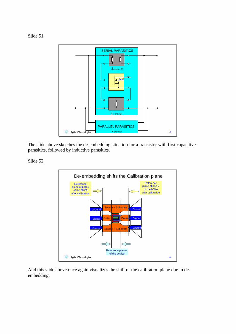
The slide above sketches the de-embedding situation for a transistor with first capacitive parasitics, followed by inductive parasitics. Slide 52
52Agilent Technologies
Source + Substrate
Gate
Ground
Ground
Ground
Ground
SignalSignal
Ground
Ground
Signal
Ground
Ground
Signal
Reference planes of the device
Reference plane of port 1 of the NWA
after calibration
Reference plane of port 2 of the NWA
after calibration
Drain
Source + Substrate
De-embedding shifts the Calibration plane
And this slide above once again visualizes the shift of the calibration plane due to de-embedding.
Slide 53
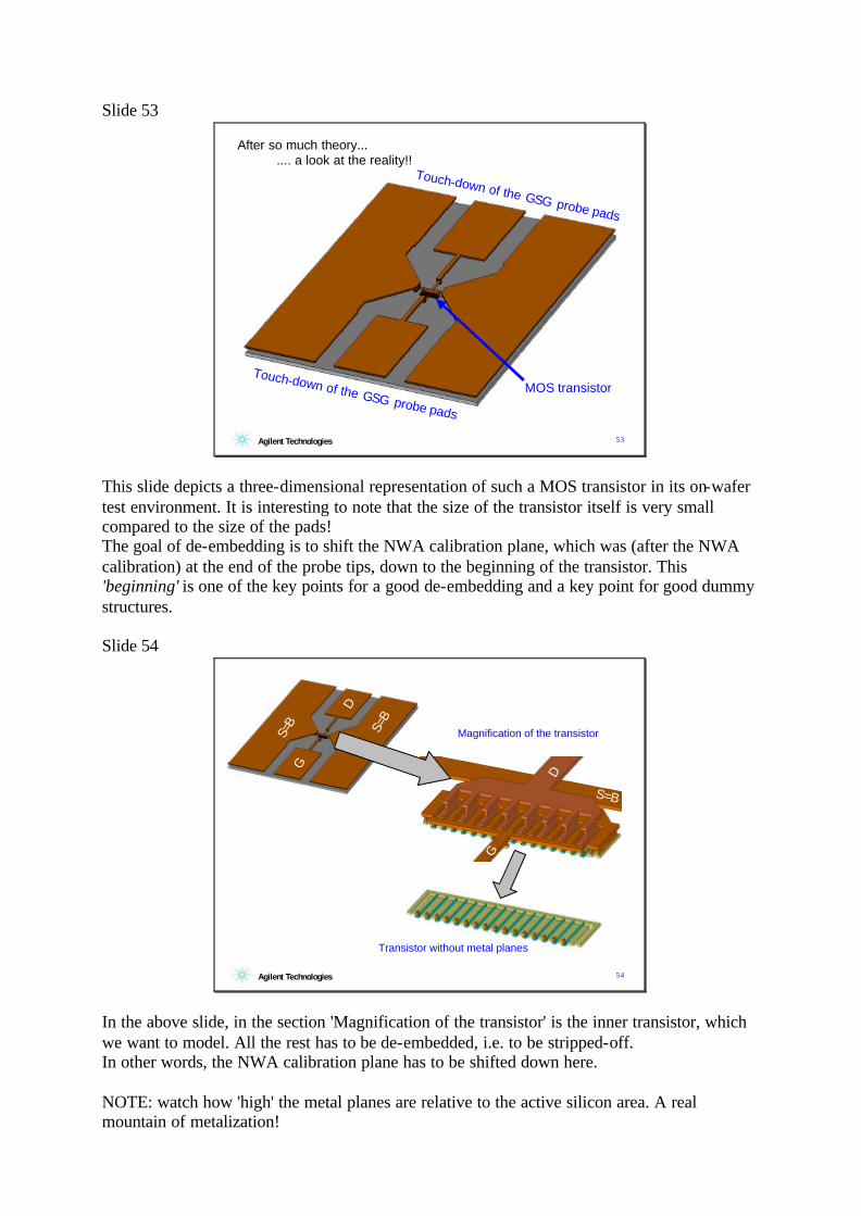
53Agilent Technologies
After so much theory....... a look at the reality!!
MOS transistorTouch-down of the GSG probe pads
Touch-down of the GSG probe pads
This slide depicts a three-dimensional representation of such a MOS transistor in its on-wafer test environment. It is interesting to note that the size of the transistor itself is very small compared to the size of the pads! The goal of de-embedding is to shift the NWA calibration plane, which was (after the NWA calibration) at the end of the probe tips, down to the beginning of the transistor. This 'beginning' is one of the key points for a good de-embedding and a key point for good dummy structures. Slide 54
54Agilent Technologies
Magnification of the transistor
Transistor without metal planes
G
D
S=B S=B
G
D
S=B
In the above slide, in the section 'Magnification of the transistor' is the inner transistor, which we want to model. All the rest has to be de-embedded, i.e. to be stripped-off. In other words, the NWA calibration plane has to be shifted down here. NOTE: watch how 'high' the metal planes are relative to the active silicon area. A real mountain of metalization!
Slide 55
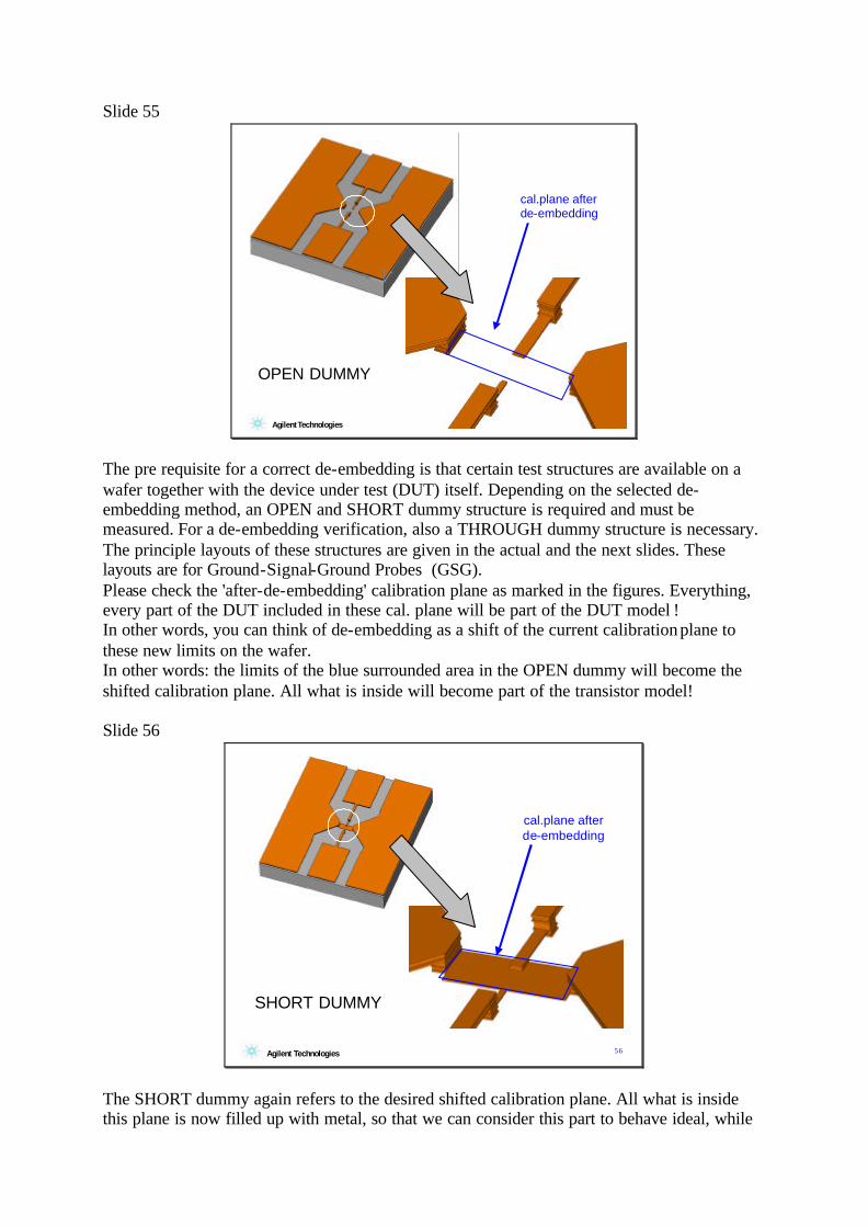
55Agilent Technologies
cal.plane afterde-embedding
OPEN DUMMY
The pre requisite for a correct de-embedding is that certain test structures are available on a wafer together with the device under test (DUT) itself. Depending on the selected de-embedding method, an OPEN and SHORT dummy structure is required and must be measured. For a de-embedding verification, also a THROUGH dummy structure is necessary. The principle layouts of these structures are given in the actual and the next slides. These layouts are for Ground-Signal-Ground Probes (GSG). Please check the 'after-de-embedding' calibration plane as marked in the figures. Everything, every part of the DUT included in these cal. plane will be part of the DUT model ! In other words, you can think of de-embedding as a shift of the current calibration plane to these new limits on the wafer. In other words: the limits of the blue surrounded area in the OPEN dummy will become the shifted calibration plane. All what is inside will become part of the transistor model! Slide 56
56Agilent Technologies
cal.plane afterde-embedding
SHORT DUMMY
The SHORT dummy again refers to the desired shifted calibration plane. All what is inside this plane is now filled up with metal, so that we can consider this part to behave ideal, while
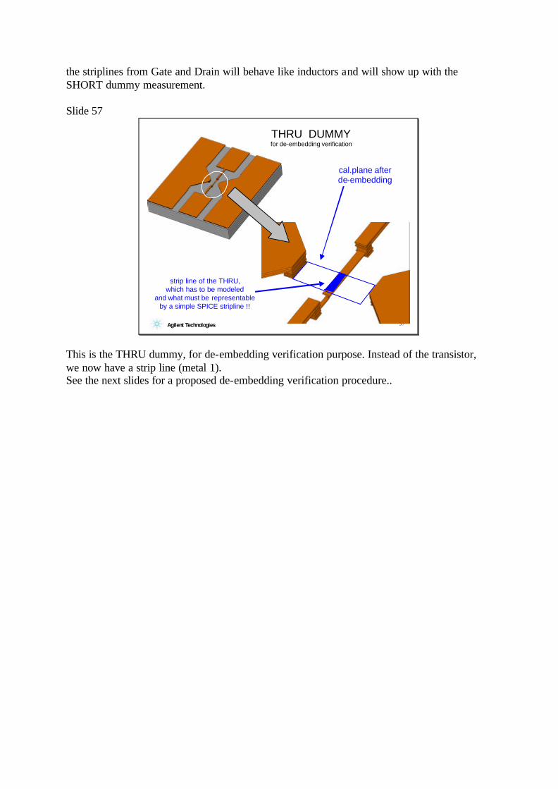
the striplines from Gate and Drain will behave like inductors and will show up with the SHORT dummy measurement. Slide 57
57Agilent Technologies
cal.plane afterde-embedding
strip line of the THRU,which has to be modeled
and what must be representableby a simple SPICE stripline !!
THRU DUMMYfor de-embedding verification
This is the THRU dummy, for de-embedding verification purpose. Instead of the transistor, we now have a strip line (metal 1). See the next slides for a proposed de-embedding verification procedure..
Slide 58
58Agilent Technologies
Another smart idea for Dummy Test Structures,avoiding the drawbacks of the SHORT metal plane
From: T.E.Kolding, O.K.Jensen, T.Larsen, Ground-Shielded Measuring Techniques for Accurate On -Wafer Characterization of RF CMOS DevicesIEEE International Conference on Microelectronic Test Structures , March 2000, p.246-251
guard planeMetal 1
Metal 2,3
OPEN
SHORT
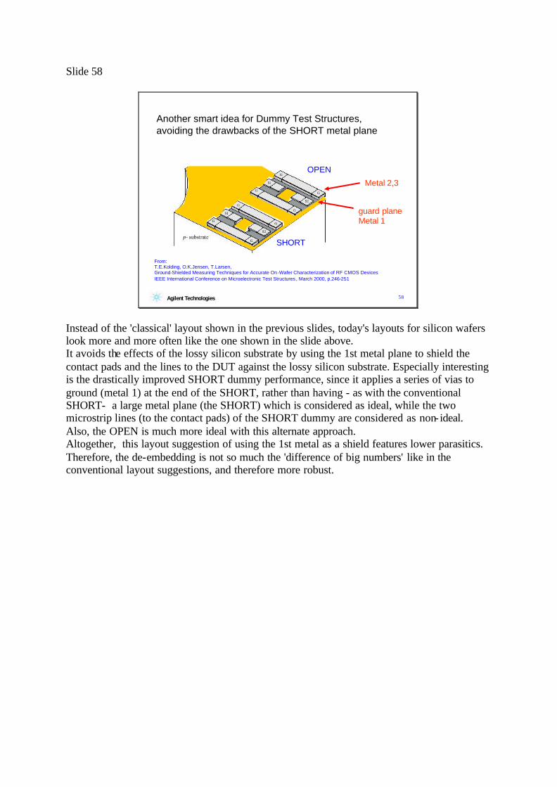
Instead of the 'classical' layout shown in the previous slides, today's layouts for silicon wafers look more and more often like the one shown in the slide above. It avoids the effects of the lossy silicon substrate by using the 1st metal plane to shield the contact pads and the lines to the DUT against the lossy silicon substrate. Especially interesting is the drastically improved SHORT dummy performance, since it applies a series of vias to ground (metal 1) at the end of the SHORT, rather than having - as with the conventional SHORT- a large metal plane (the SHORT) which is considered as ideal, while the two microstrip lines (to the contact pads) of the SHORT dummy are considered as non- ideal. Also, the OPEN is much more ideal with this alternate approach. Altogether, this layout suggestion of using the 1st metal as a shield features lower parasitics. Therefore, the de-embedding is not so much the 'difference of big numbers' like in the conventional layout suggestions, and therefore more robust.
Slide 59
59Agilent Technologies
Verifying the de-embedding
measured
deembedded
TD
Z0
deembedded
measured
Sxx
Sxy
e.g.: Z0 =35ΩTD=1.14ps
Z0, TD
layout
equivalent circuit
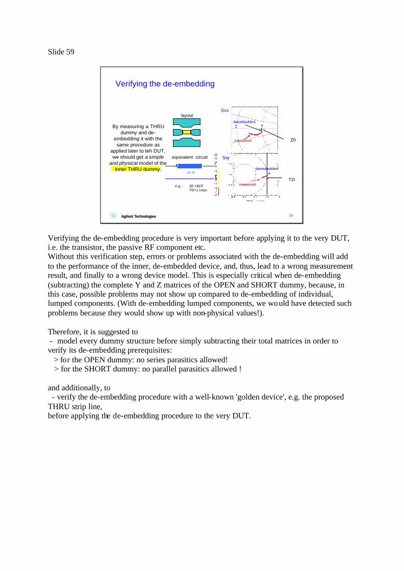
By measuring a THRU dummy and de-
embedding it with the same procedure as
applied later to teh DUT, we should get a simple
and physical model of the inner THRU dummy.
Verifying the de-embedding procedure is very important before applying it to the very DUT, i.e. the transistor, the passive RF component etc. Without this verification step, errors or problems associated with the de-embedding will add to the performance of the inner, de-embedded device, and, thus, lead to a wrong measurement result, and finally to a wrong device model. This is especially critical when de-embedding (subtracting) the complete Y and Z matrices of the OPEN and SHORT dummy, because, in this case, possible problems may not show up compared to de-embedding of individual, lumped components. (With de-embedding lumped components, we would have detected such problems because they would show up with non-physical values!). Therefore, it is suggested to - model every dummy structure before simply subtracting their total matrices in order to verify its de-embedding prerequisites: > for the OPEN dummy: no series parasitics allowed! > for the SHORT dummy: no parallel parasitics allowed ! and additionally, to - verify the de-embedding procedure with a well-known 'golden device', e.g. the proposed THRU strip line, before applying the de-embedding procedure to the very DUT.
Slide 60
60Agilent Technologies
un-deembedded DUTdeembedded DUT
over deembedded
correctly deembedded
under deembedded
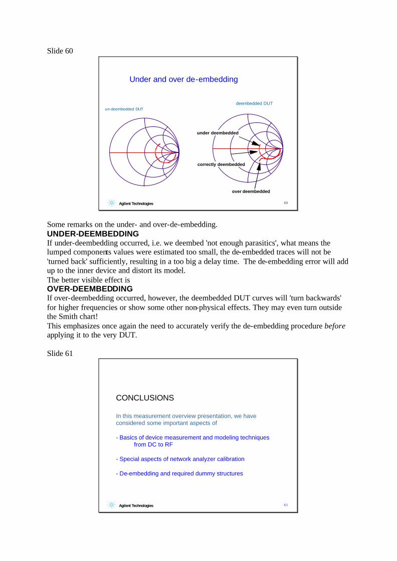
Under and over de-embedding
Some remarks on the under- and over-de-embedding. UNDER-DEEMBEDDING If under-deembedding occurred, i.e. we deembed 'not enough parasitics', what means the lumped components values were estimated too small, the de-embedded traces will not be 'turned back' sufficiently, resulting in a too big a delay time. The de-embedding error will add up to the inner device and distort its model. The better visible effect is OVER-DEEMBEDDING If over-deembedding occurred, however, the deembedded DUT curves will 'turn backwards' for higher frequencies or show some other non-physical effects. They may even turn outside the Smith chart! This emphasizes once again the need to accurately verify the de-embedding procedure before applying it to the very DUT. Slide 61
61Agilent Technologies
CONCLUSIONS
In this measurement overview presentation, we have considered some important aspects of
- Basics of device measurement and modeling techniques from DC to RF
- Special aspects of network analyzer calibration
- De-embedding and required dummy structures

www.agilent.com/fi nd/emailupdatesGet the latest information on the products and applications you select.
www.agilent.com/fi nd/agilentdirectQuickly choose and use your test equipment solutions with confi dence.
Agilent Email Updates
Agilent Direct
www.agilent.comFor more information on Agilent Technologies’ products, applications or services, please contact your local Agilent office. The complete list is available at:www.agilent.com/fi nd/contactus
AmericasCanada (877) 894-4414 Latin America 305 269 7500United States (800) 829-4444
Asia Pacifi cAustralia 1 800 629 485China 800 810 0189Hong Kong 800 938 693India 1 800 112 929Japan 0120 (421) 345Korea 080 769 0800Malaysia 1 800 888 848Singapore 1 800 375 8100Taiwan 0800 047 866Thailand 1 800 226 008
Europe & Middle EastAustria 0820 87 44 11Belgium 32 (0) 2 404 93 40 Denmark 45 70 13 15 15Finland 358 (0) 10 855 2100France 0825 010 700* *0.125 €/minuteGermany 01805 24 6333** **0.14 €/minuteIreland 1890 924 204Israel 972-3-9288-504/544Italy 39 02 92 60 8484Netherlands 31 (0) 20 547 2111Spain 34 (91) 631 3300Sweden 0200-88 22 55Switzerland 0800 80 53 53United Kingdom 44 (0) 118 9276201Other European Countries: www.agilent.com/fi nd/contactusRevised: March 27, 2008
Product specifi cations and descriptions in this document subject to change without notice.
© Agilent Technologies, Inc. 2008
For more information about Agilent EEsof EDA, visit:
www.agilent.com/fi nd/eesof


![[XLS] · Web viewAC UARINI AC URUCARA AC URUCURITUBA AC AGRESTE AC AMAPA AC BAILIQUE AC BEIROL AC CALCOENE AC CENTRO AC CUTIAS AC EQUATORIAL AC FERREIRA GOMES AC ITAUBAL AC LARANJAL](https://img.pdfslide.net/doc/110x75/5c5be47c09d3f245368c84d6/xls-web-viewac-uarini-ac-urucara-ac-urucurituba-ac-agreste-ac-amapa-ac-bailique.jpg)