Embed Size (px)
Citation preview
A-1 Appendix A - Digital Logic
Department of Information Technology, Radford University ITEC 352 Computer Organization
Principles of Computer ArchitectureMiles Murdocca and Vincent Heuring
Appendix A: Digital Logic
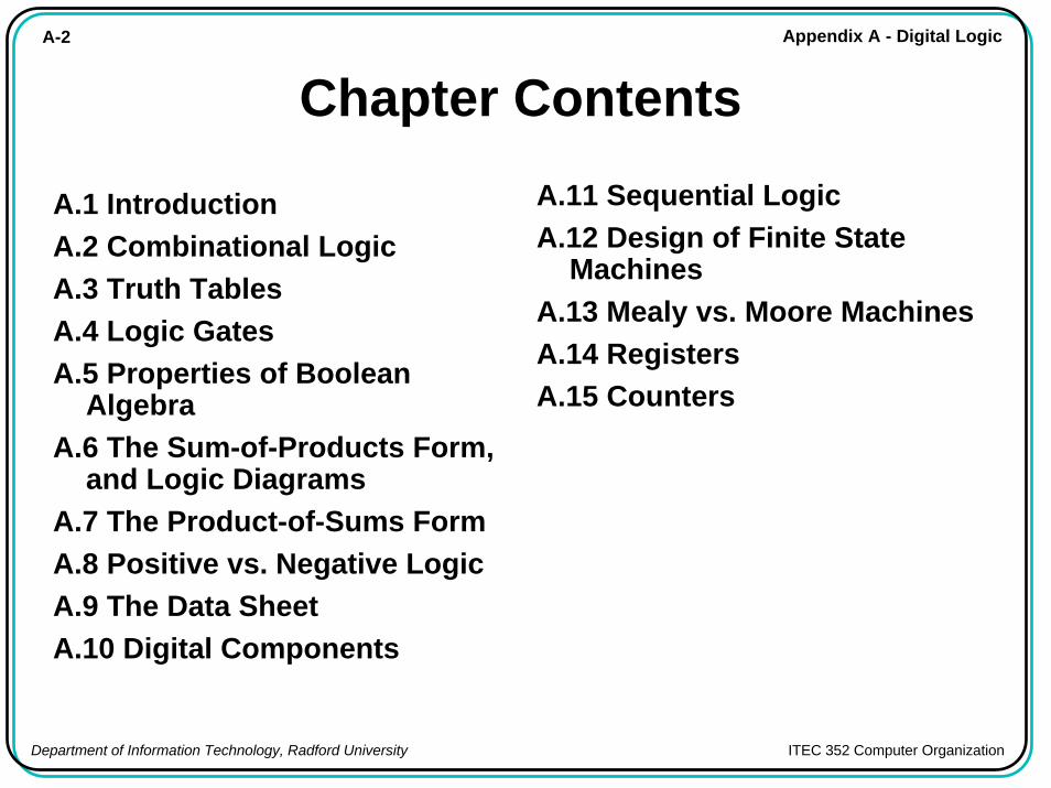
A-2 Appendix A - Digital Logic
Department of Information Technology, Radford University ITEC 352 Computer Organization
Chapter Contents
A.1 IntroductionA.2 Combinational LogicA.3 Truth TablesA.4 Logic GatesA.5 Properties of Boolean
AlgebraA.6 The Sum-of-Products Form,
and Logic DiagramsA.7 The Product-of-Sums FormA.8 Positive vs. Negative LogicA.9 The Data SheetA.10 Digital Components
A.11 Sequential LogicA.12 Design of Finite State
MachinesA.13 Mealy vs. Moore MachinesA.14 RegistersA.15 Counters
A-3 Appendix A - Digital Logic
Department of Information Technology, Radford University ITEC 352 Computer Organization
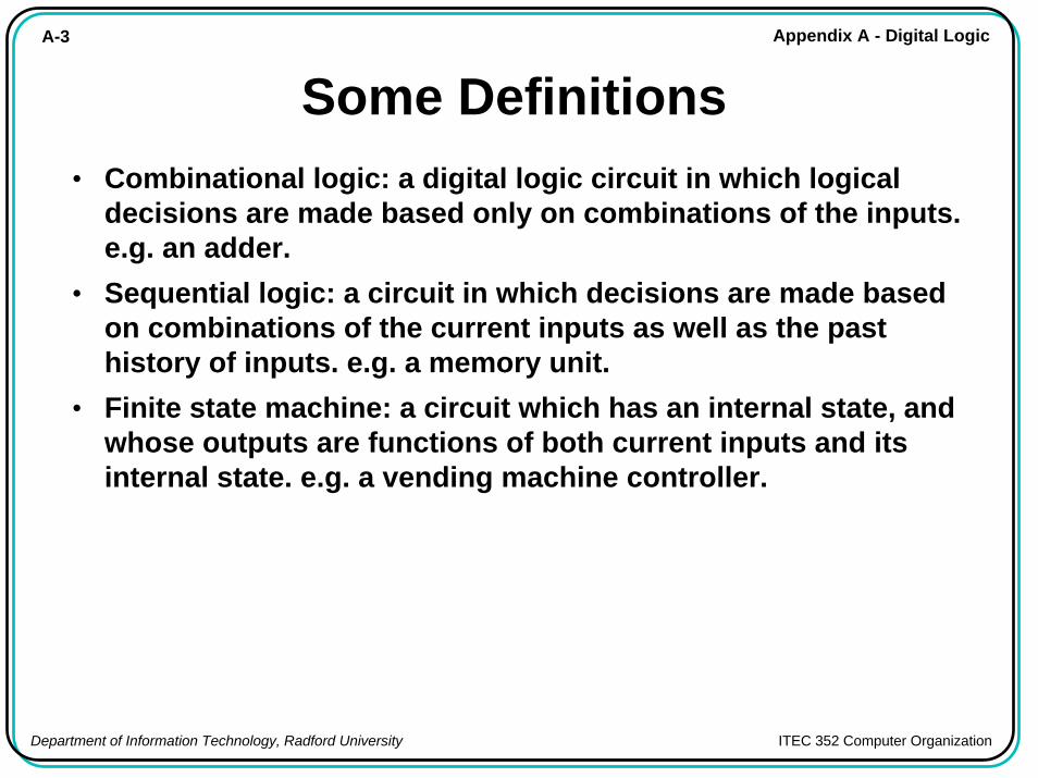
Some Definitions• Combinational logic: a digital logic circuit in which logical
decisions are made based only on combinations of the inputs. e.g. an adder.
• Sequential logic: a circuit in which decisions are made based on combinations of the current inputs as well as the past history of inputs. e.g. a memory unit.
• Finite state machine: a circuit which has an internal state, andwhose outputs are functions of both current inputs and its internal state. e.g. a vending machine controller.
A-4 Appendix A - Digital Logic
Department of Information Technology, Radford University ITEC 352 Computer Organization
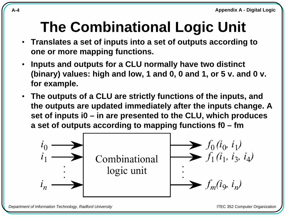
The Combinational Logic Unit• Translates a set of inputs into a set of outputs according to
one or more mapping functions. • Inputs and outputs for a CLU normally have two distinct
(binary) values: high and low, 1 and 0, 0 and 1, or 5 v. and 0 v. for example.
• The outputs of a CLU are strictly functions of the inputs, and the outputs are updated immediately after the inputs change. A set of inputs i0 – in are presented to the CLU, which produces a set of outputs according to mapping functions f0 – fm
A-5 Appendix A - Digital Logic
Department of Information Technology, Radford University ITEC 352 Computer Organization
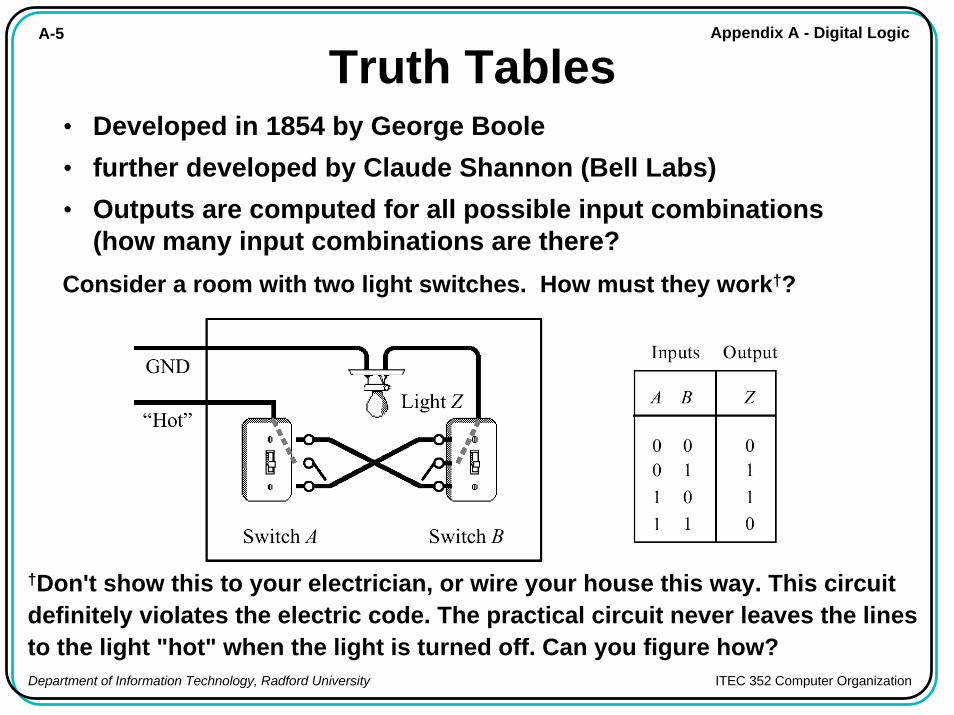
Truth Tables• Developed in 1854 by George Boole• further developed by Claude Shannon (Bell Labs)• Outputs are computed for all possible input combinations
(how many input combinations are there?Consider a room with two light switches. How must they work†?
†Don't show this to your electrician, or wire your house this way. This circuit definitely violates the electric code. The practical circuit never leaves the lines to the light "hot" when the light is turned off. Can you figure how?
A-6 Appendix A - Digital Logic
Department of Information Technology, Radford University ITEC 352 Computer Organization
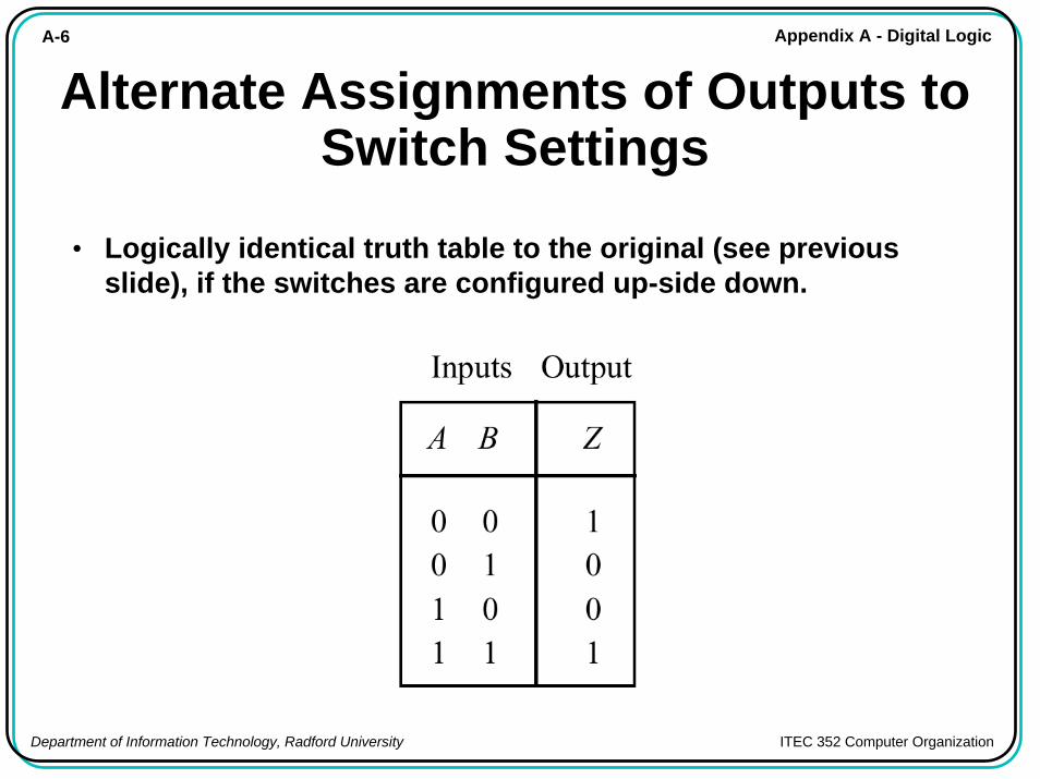
Alternate Assignments of Outputs to Switch Settings
• Logically identical truth table to the original (see previous slide), if the switches are configured up-side down.
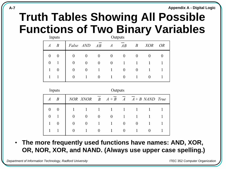
A-7 Appendix A - Digital Logic
Department of Information Technology, Radford University ITEC 352 Computer Organization
Truth Tables Showing All Possible Functions of Two Binary Variables
• The more frequently used functions have names: AND, XOR, OR, NOR, XOR, and NAND. (Always use upper case spelling.)
A-8 Appendix A - Digital Logic
Department of Information Technology, Radford University ITEC 352 Computer Organization
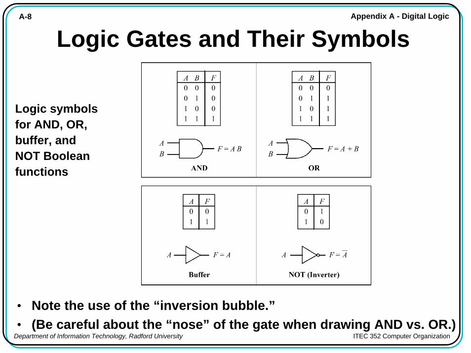
Logic Gates and Their Symbols
• Note the use of the “inversion bubble.”• (Be careful about the “nose” of the gate when drawing AND vs. OR.)
Logic symbols for AND, OR, buffer, and NOT Boolean functions
A-9 Appendix A - Digital Logic
Department of Information Technology, Radford University ITEC 352 Computer Organization
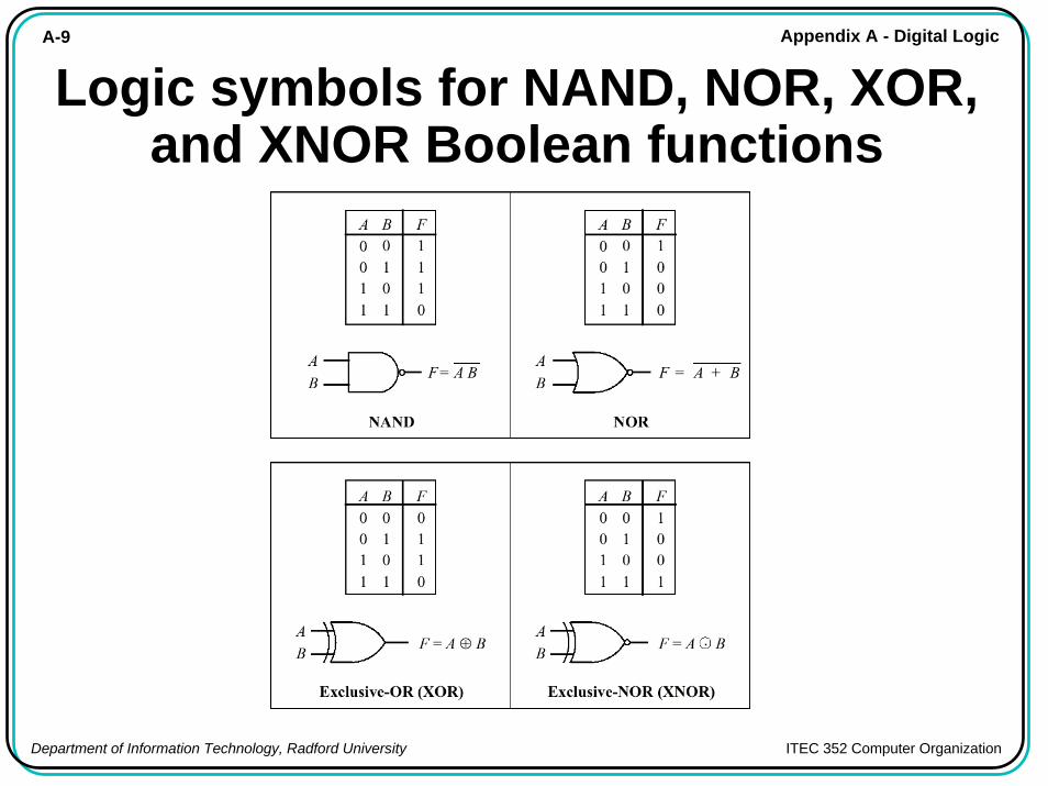
Logic symbols for NAND, NOR, XOR, and XNOR Boolean functions
A-10 Appendix A - Digital Logic
Department of Information Technology, Radford University ITEC 352 Computer Organization
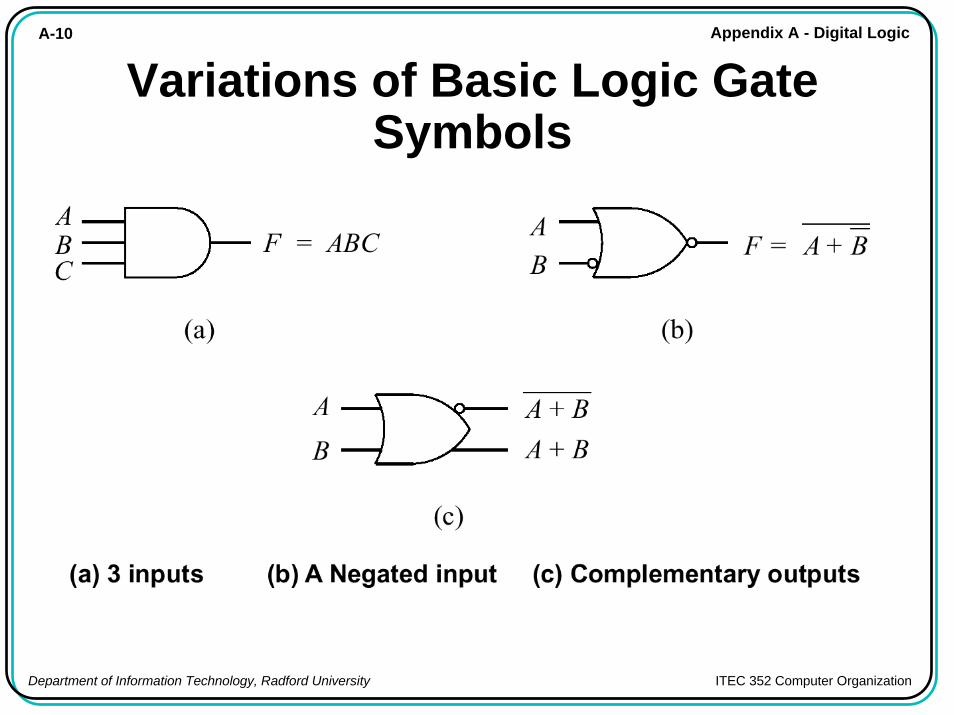
Variations of Basic Logic Gate Symbols
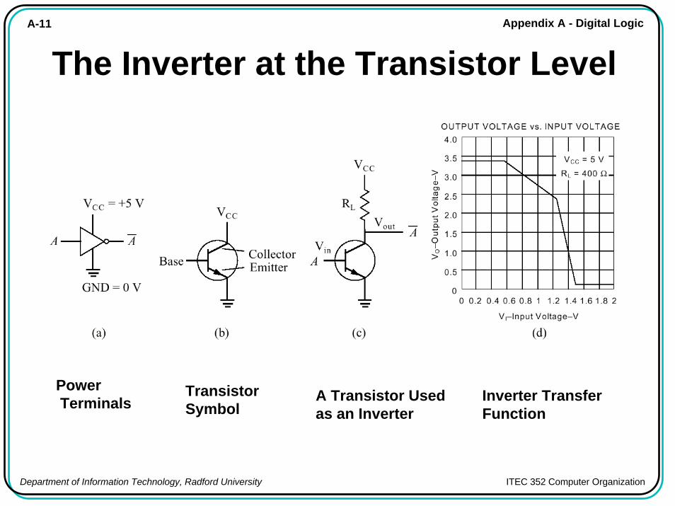
A-11 Appendix A - Digital Logic
Department of Information Technology, Radford University ITEC 352 Computer Organization
The Inverter at the Transistor Level
Transistor Symbol
PowerTerminals A Transistor Used
as an InverterInverter TransferFunction
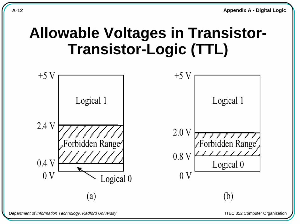
A-12 Appendix A - Digital Logic
Department of Information Technology, Radford University ITEC 352 Computer Organization
Allowable Voltages in Transistor-Transistor-Logic (TTL)
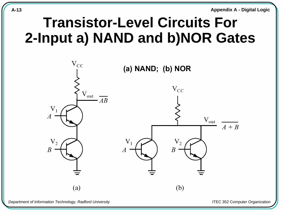
A-13 Appendix A - Digital Logic
Department of Information Technology, Radford University ITEC 352 Computer Organization
Transistor-Level Circuits For2-Input a) NAND and b)NOR Gates
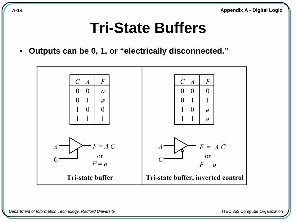
A-14 Appendix A - Digital Logic
Department of Information Technology, Radford University ITEC 352 Computer Organization
Tri-State Buffers• Outputs can be 0, 1, or “electrically disconnected.”
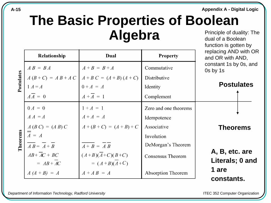
A-15 Appendix A - Digital Logic
Department of Information Technology, Radford University ITEC 352 Computer Organization
The Basic Properties of Boolean Algebra
Postulates
Theorems
A, B, etc. are Literals; 0 and 1 are constants.
Principle of duality: The dual of a Boolean function is gotten by replacing AND with OR and OR with AND, constant 1s by 0s, and 0s by 1s
A-16 Appendix A - Digital Logic
Department of Information Technology, Radford University ITEC 352 Computer Organization
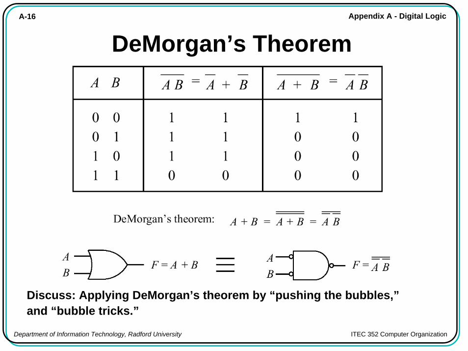
DeMorgan’s Theorem
Discuss: Applying DeMorgan’s theorem by “pushing the bubbles,”and “bubble tricks.”
A-17 Appendix A - Digital Logic
Department of Information Technology, Radford University ITEC 352 Computer Organization
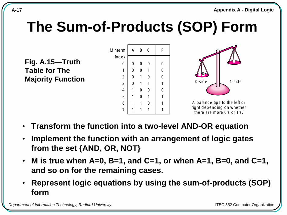
The Sum-of-Products (SOP) Form
• Transform the function into a two-level AND-OR equation• Implement the function with an arrangement of logic gates
from the set {AND, OR, NOT}• M is true when A=0, B=1, and C=1, or when A=1, B=0, and C=1,
and so on for the remaining cases.• Represent logic equations by using the sum-of-products (SOP)
form
Fig. A.15—Truth Table for The Majority Function
A B C FMinterm
Index
0 0 0 0
0 0 1 0
0 1 0 0
0 1 1 1
1 0 0 0
1 0 1 1
1 1 0 1
1 1 1 1
0
1
2
3
4
5
6
7
1
0
0-side 1-side
0
A balance tips to the left or right depending on whether
there are more 0’s or 1’s.
A-18 Appendix A - Digital Logic
Department of Information Technology, Radford University ITEC 352 Computer Organization
The SOP Form of the Majority Gate
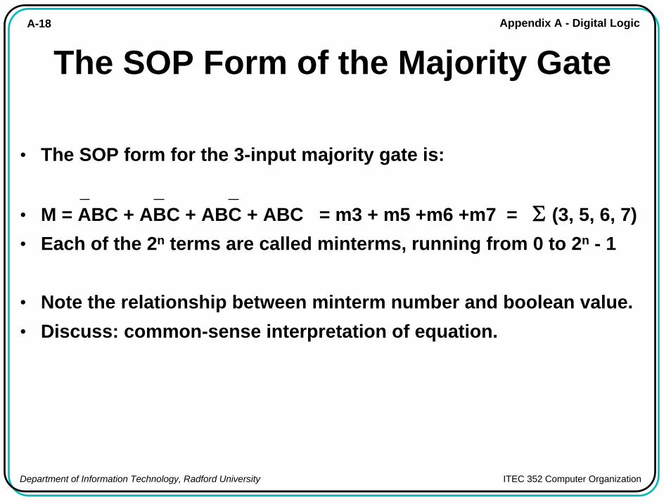
• The SOP form for the 3-input majority gate is:
• M = ABC + ABC + ABC + ABC = m3 + m5 +m6 +m7 = Σ (3, 5, 6, 7)• Each of the 2n terms are called minterms, running from 0 to 2n - 1
• Note the relationship between minterm number and boolean value.• Discuss: common-sense interpretation of equation.
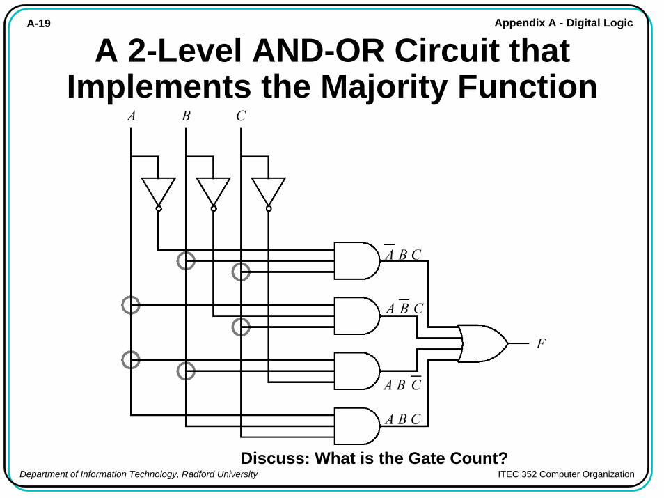
A-19 Appendix A - Digital Logic
Department of Information Technology, Radford University ITEC 352 Computer Organization
A 2-Level AND-OR Circuit that Implements the Majority Function
Discuss: What is the Gate Count?
A-20 Appendix A - Digital Logic
Department of Information Technology, Radford University ITEC 352 Computer Organization
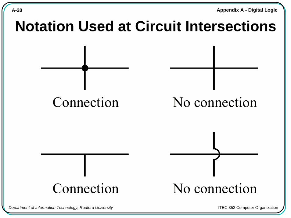
Notation Used at Circuit Intersections
A-21 Appendix A - Digital Logic
Department of Information Technology, Radford University ITEC 352 Computer Organization
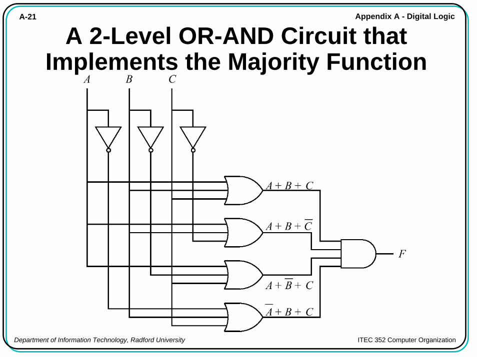
A 2-Level OR-AND Circuit that Implements the Majority Function
A-22 Appendix A - Digital Logic
Department of Information Technology, Radford University ITEC 352 Computer Organization
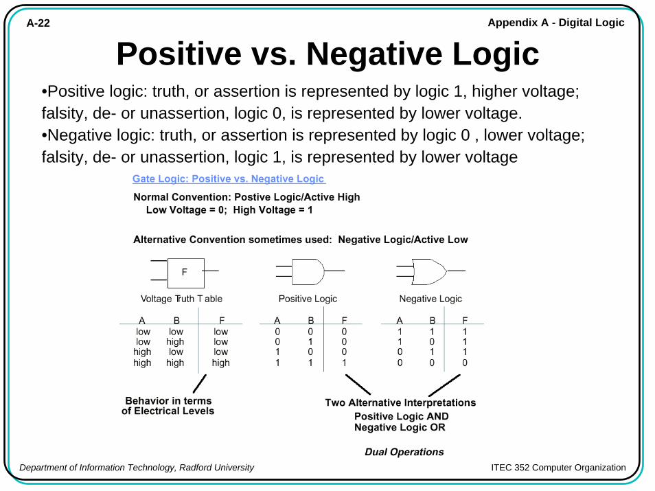
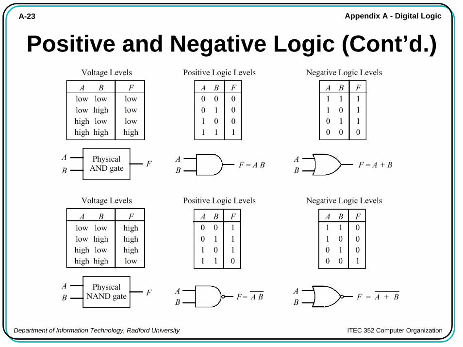
Positive vs. Negative Logic•Positive logic: truth, or assertion is represented by logic 1, higher voltage; falsity, de- or unassertion, logic 0, is represented by lower voltage.•Negative logic: truth, or assertion is represented by logic 0 , lower voltage; falsity, de- or unassertion, logic 1, is represented by lower voltage
A-23 Appendix A - Digital Logic
Department of Information Technology, Radford University ITEC 352 Computer Organization
Positive and Negative Logic (Cont’d.)
A-24 Appendix A - Digital Logic
Department of Information Technology, Radford University ITEC 352 Computer Organization
Bubble Matching
• Active low signals are signified by a prime or overbar or /.• Active high: enable• Active low: enable’, enable, enable/ • Discuss microwave oven control:• Active high: Heat = DoorClosed • Start• Active low: ? (hint: begin with AND gate as before.)
A-25 Appendix A - Digital Logic
Department of Information Technology, Radford University ITEC 352 Computer Organization
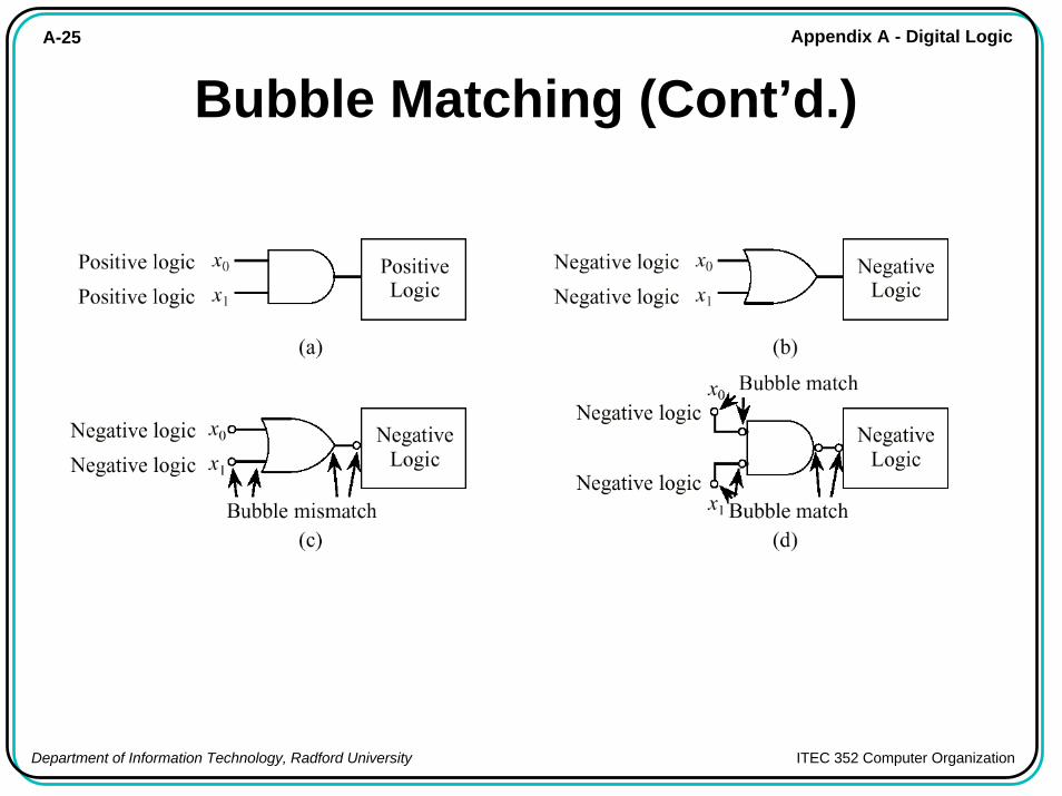
Bubble Matching (Cont’d.)
A-26 Appendix A - Digital Logic
Department of Information Technology, Radford University ITEC 352 Computer Organization
Digital Components
• High level digital circuit designs are normally made using collections of logic gates referred to as components, rather than using individual logic gates. The majority function can be viewed as a component.
• Levels of integration (numbers of gates) in an integrated circuit (IC):
• Small scale integration (SSI): 10-100 gates. • Medium scale integration (MSI): 100 to 1000 gates.• Large scale integration (LSI): 1000-10,000 logic gates.• Very large scale integration (VLSI): 10,000-upward.• These levels are approximate, but the distinctions are useful in
comparing the relative complexity of circuits.• Let us consider several useful MSI components:
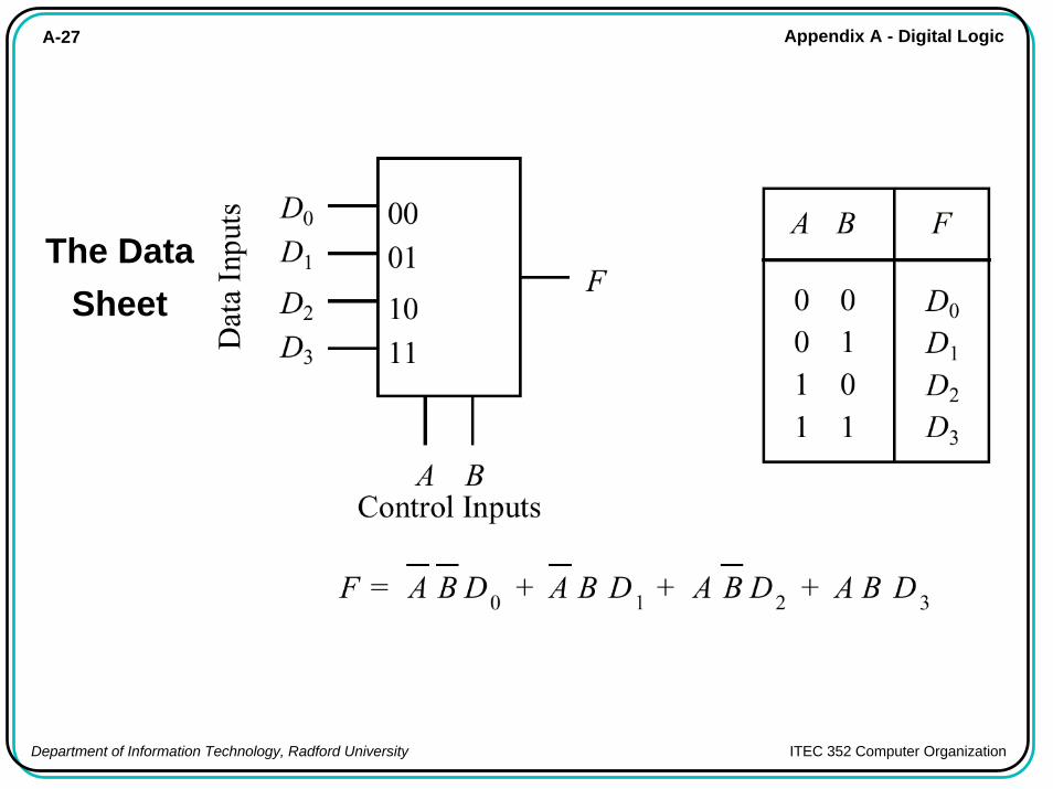
A-27 Appendix A - Digital Logic
Department of Information Technology, Radford University ITEC 352 Computer Organization
The Data Sheet
A-28 Appendix A - Digital Logic
Department of Information Technology, Radford University ITEC 352 Computer Organization
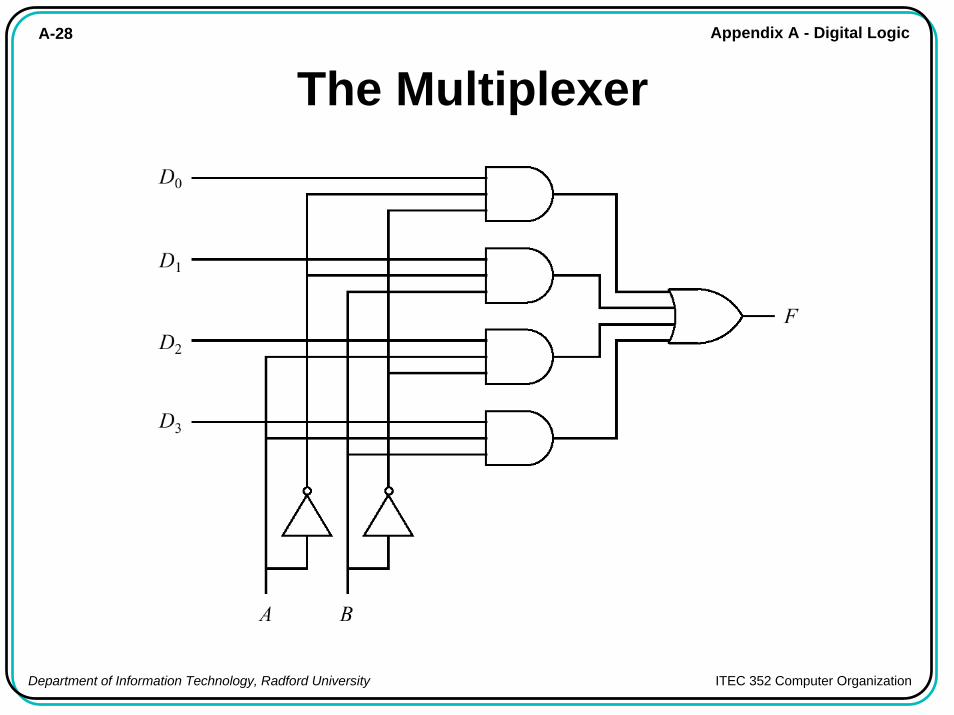
The Multiplexer
A-29 Appendix A - Digital Logic
Department of Information Technology, Radford University ITEC 352 Computer Organization
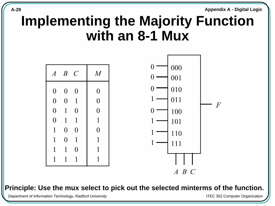
Implementing the Majority Function with an 8-1 Mux
Principle: Use the mux select to pick out the selected minterms of the function.
A-30 Appendix A - Digital Logic
Department of Information Technology, Radford University ITEC 352 Computer Organization
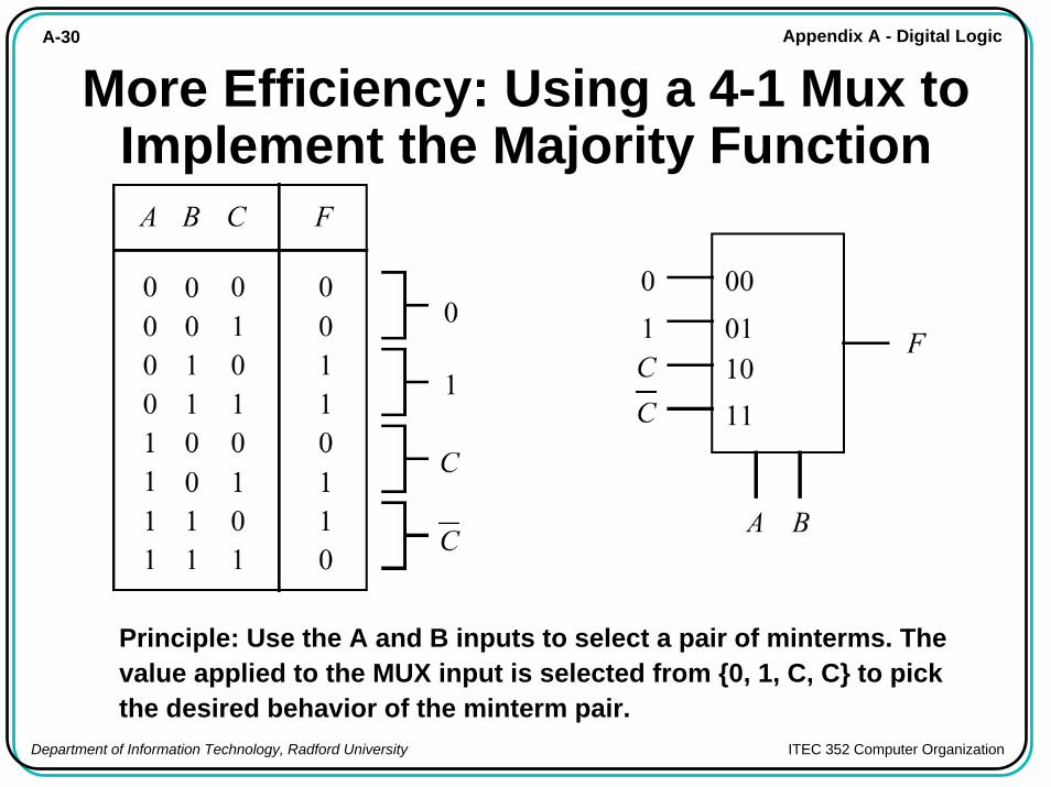
More Efficiency: Using a 4-1 Mux to Implement the Majority Function
Principle: Use the A and B inputs to select a pair of minterms. The value applied to the MUX input is selected from {0, 1, C, C} to pick the desired behavior of the minterm pair.
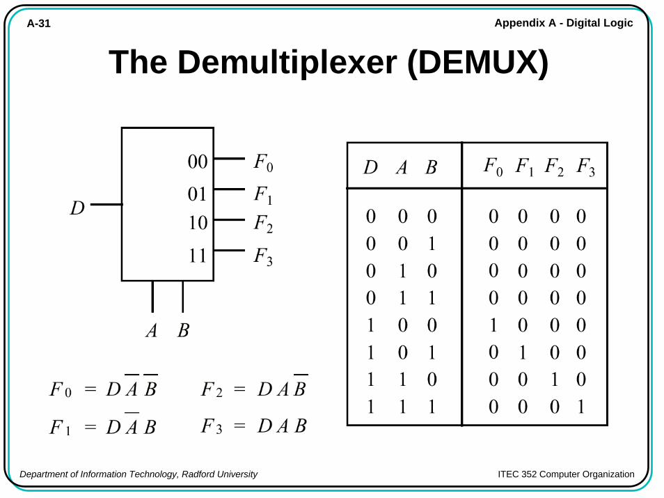
A-31 Appendix A - Digital Logic
Department of Information Technology, Radford University ITEC 352 Computer Organization
The Demultiplexer (DEMUX)
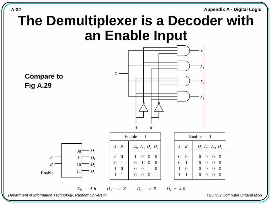
A-32 Appendix A - Digital Logic
Department of Information Technology, Radford University ITEC 352 Computer Organization
The Demultiplexer is a Decoder with an Enable Input
Compare toFig A.29
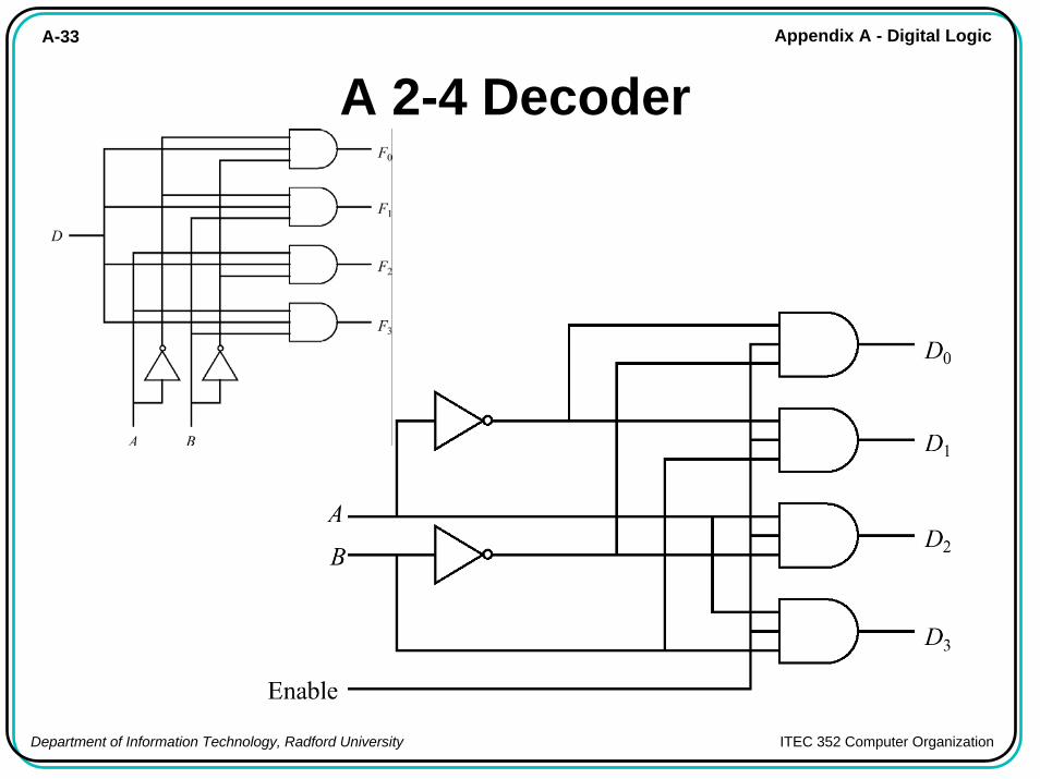
A-33 Appendix A - Digital Logic
Department of Information Technology, Radford University ITEC 352 Computer Organization
A 2-4 Decoder
A-34 Appendix A - Digital Logic
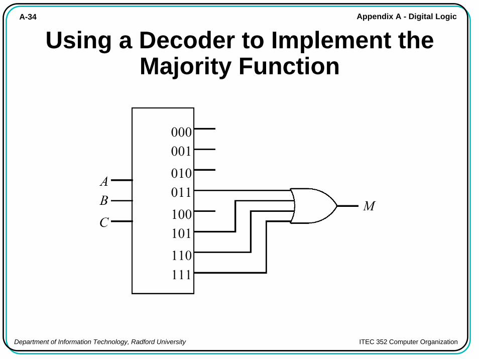
Department of Information Technology, Radford University ITEC 352 Computer Organization
Using a Decoder to Implement the Majority Function
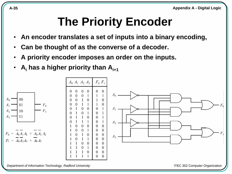
A-35 Appendix A - Digital Logic
Department of Information Technology, Radford University ITEC 352 Computer Organization
The Priority Encoder• An encoder translates a set of inputs into a binary encoding, • Can be thought of as the converse of a decoder. • A priority encoder imposes an order on the inputs.• Ai has a higher priority than Ai+1
A-36 Appendix A - Digital Logic
Department of Information Technology, Radford University ITEC 352 Computer Organization
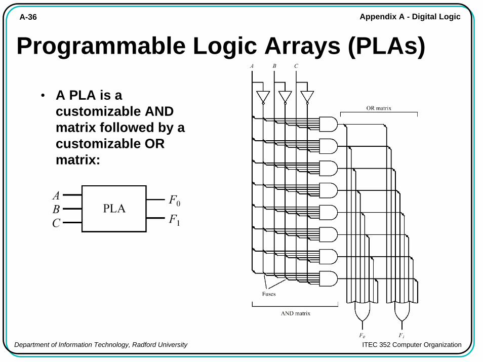
Programmable Logic Arrays (PLAs)
• A PLA is a customizable AND matrix followed by a customizable OR matrix:
A-37 Appendix A - Digital Logic
Department of Information Technology, Radford University ITEC 352 Computer Organization
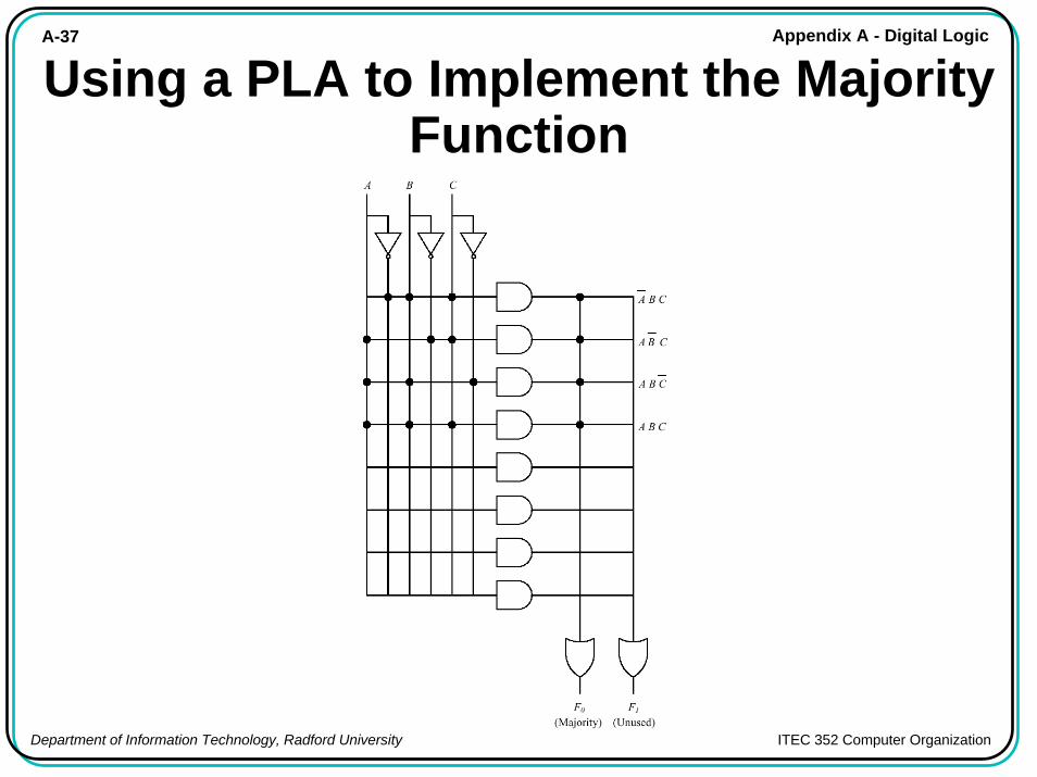
Using a PLA to Implement the Majority Function
A-38 Appendix A - Digital Logic
Department of Information Technology, Radford University ITEC 352 Computer Organization
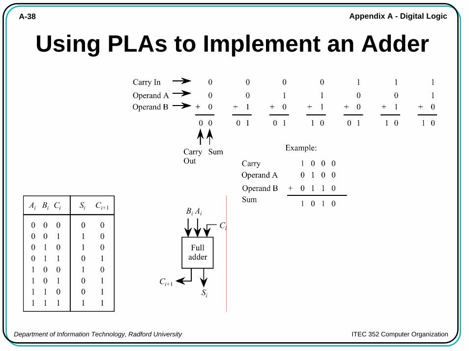
Using PLAs to Implement an Adder
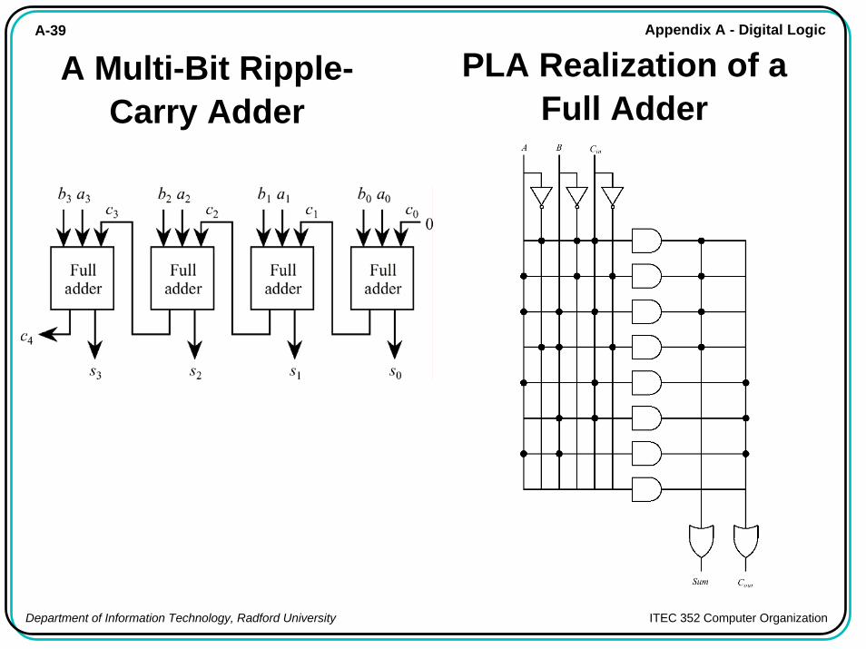
A-39 Appendix A - Digital Logic
Department of Information Technology, Radford University ITEC 352 Computer Organization
A Multi-Bit Ripple-Carry Adder
PLA Realization of a Full Adder
A-40 Appendix A - Digital Logic
Department of Information Technology, Radford University ITEC 352 Computer Organization
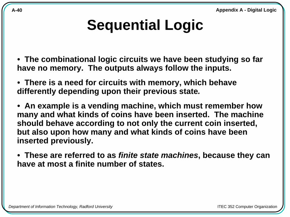
Sequential Logic
• The combinational logic circuits we have been studying so far have no memory. The outputs always follow the inputs.
• There is a need for circuits with memory, which behave differently depending upon their previous state.
• An example is a vending machine, which must remember how many and what kinds of coins have been inserted. The machine should behave according to not only the current coin inserted, but also upon how many and what kinds of coins have been inserted previously.
• These are referred to as finite state machines, because they can have at most a finite number of states.
A-41 Appendix A - Digital Logic
Department of Information Technology, Radford University ITEC 352 Computer Organization
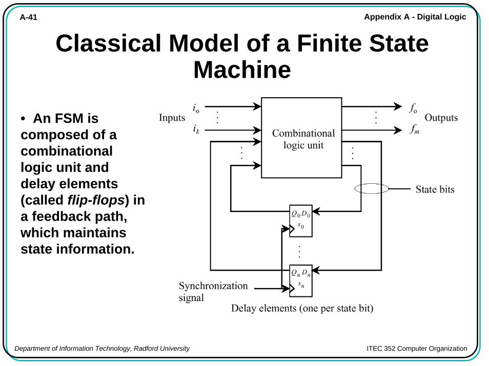
Classical Model of a Finite State Machine
• An FSM is composed of a combinational logic unit and delay elements (called flip-flops) in a feedback path, which maintains state information.
A-42 Appendix A - Digital Logic
Department of Information Technology, Radford University ITEC 352 Computer Organization
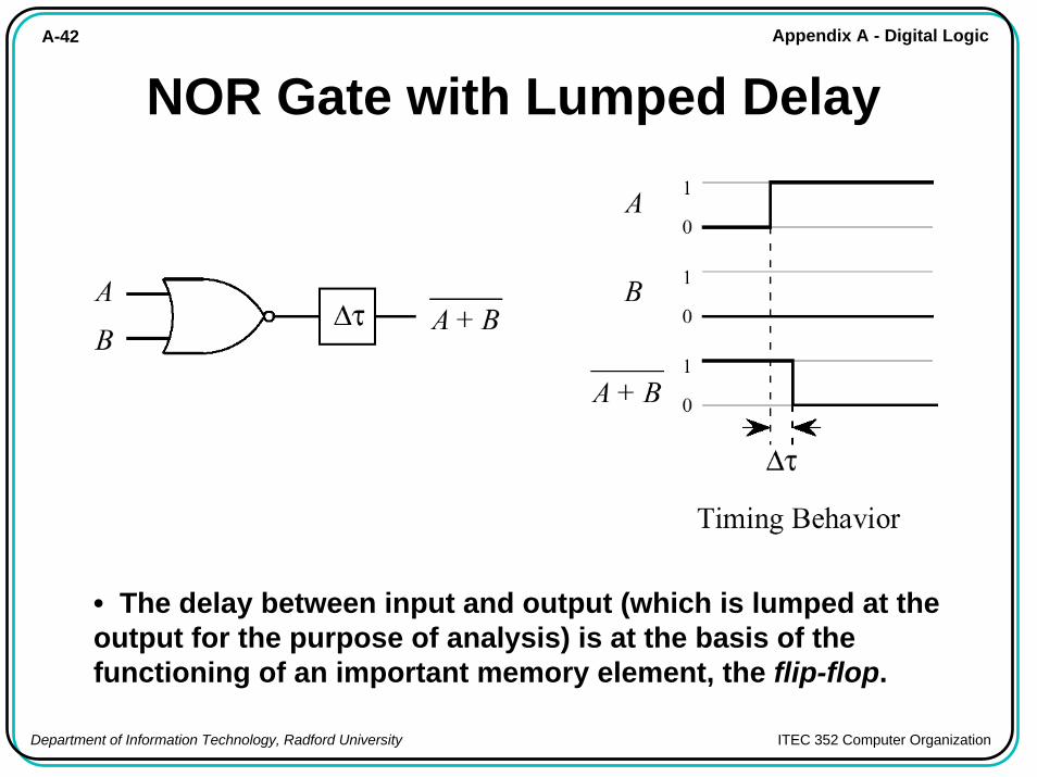
NOR Gate with Lumped Delay
• The delay between input and output (which is lumped at the output for the purpose of analysis) is at the basis of the functioning of an important memory element, the flip-flop.
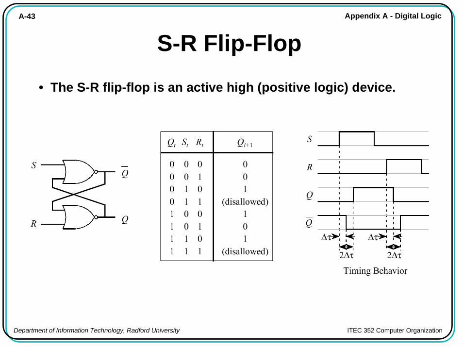
A-43 Appendix A - Digital Logic
Department of Information Technology, Radford University ITEC 352 Computer Organization
S-R Flip-Flop
• The S-R flip-flop is an active high (positive logic) device.
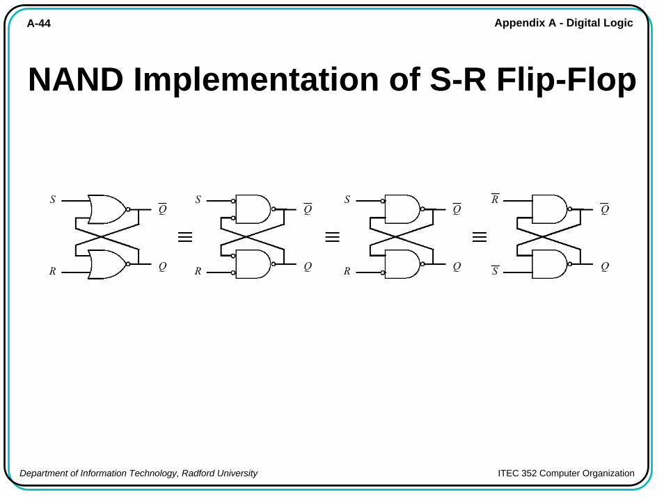
A-44 Appendix A - Digital Logic
Department of Information Technology, Radford University ITEC 352 Computer Organization
NAND Implementation of S-R Flip-Flop
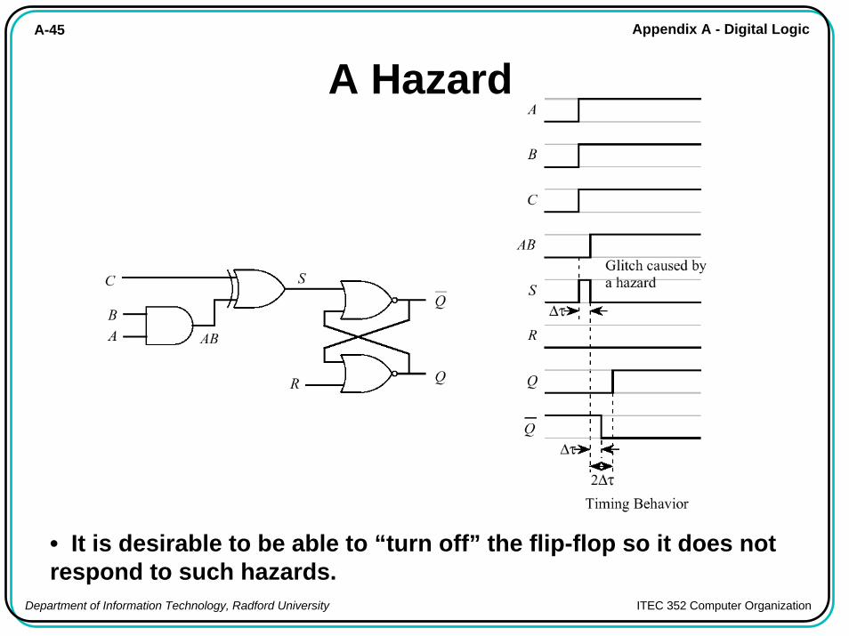
A-45 Appendix A - Digital Logic
Department of Information Technology, Radford University ITEC 352 Computer Organization
A Hazard
• It is desirable to be able to “turn off” the flip-flop so it does not respond to such hazards.
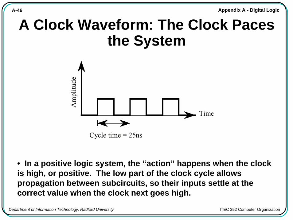
A-46 Appendix A - Digital Logic
Department of Information Technology, Radford University ITEC 352 Computer Organization
A Clock Waveform: The Clock Paces the System
• In a positive logic system, the “action” happens when the clock is high, or positive. The low part of the clock cycle allows propagation between subcircuits, so their inputs settle at the correct value when the clock next goes high.
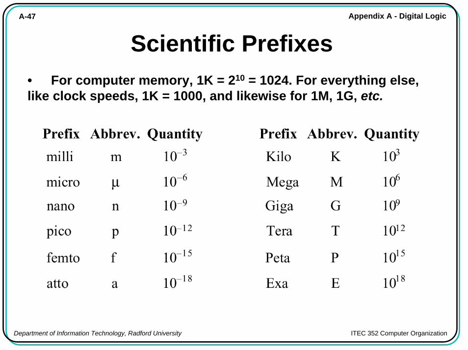
A-47 Appendix A - Digital Logic
Department of Information Technology, Radford University ITEC 352 Computer Organization
Scientific Prefixes• For computer memory, 1K = 210 = 1024. For everything else, like clock speeds, 1K = 1000, and likewise for 1M, 1G, etc.
A-48 Appendix A - Digital Logic
Department of Information Technology, Radford University ITEC 352 Computer Organization
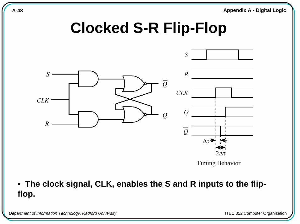
Clocked S-R Flip-Flop
• The clock signal, CLK, enables the S and R inputs to the flip-flop.
A-49 Appendix A - Digital Logic
Department of Information Technology, Radford University ITEC 352 Computer Organization
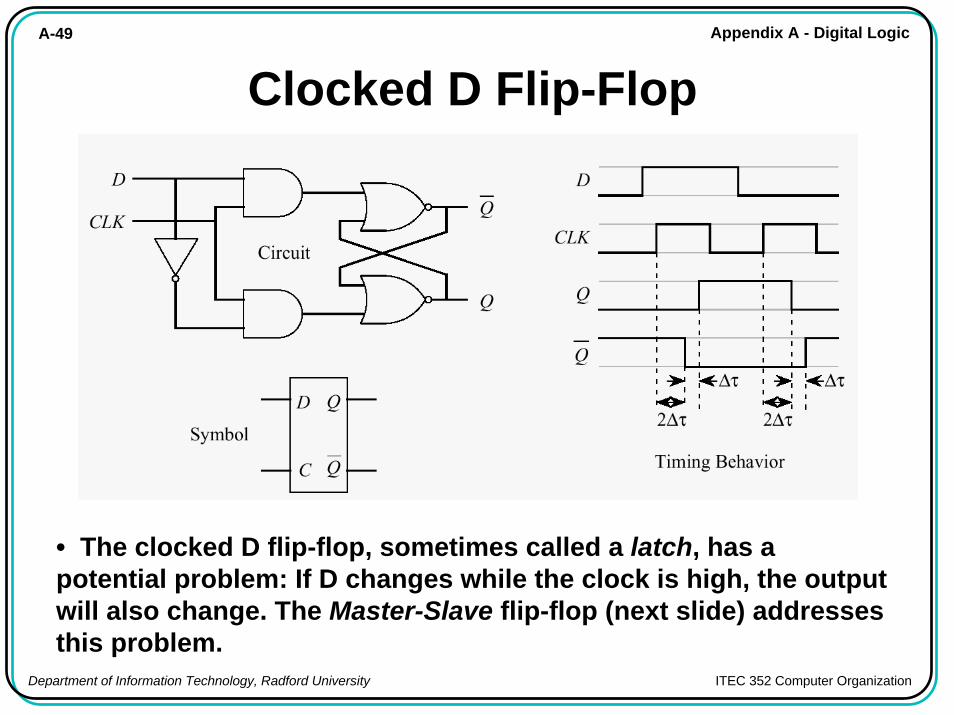
Clocked D Flip-Flop
• The clocked D flip-flop, sometimes called a latch, has a potential problem: If D changes while the clock is high, the output will also change. The Master-Slave flip-flop (next slide) addresses this problem.
A-50 Appendix A - Digital Logic
Department of Information Technology, Radford University ITEC 352 Computer Organization
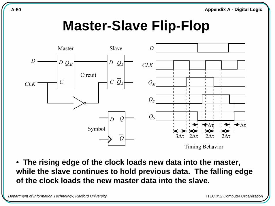
Master-Slave Flip-Flop
• The rising edge of the clock loads new data into the master, while the slave continues to hold previous data. The falling edge of the clock loads the new master data into the slave.
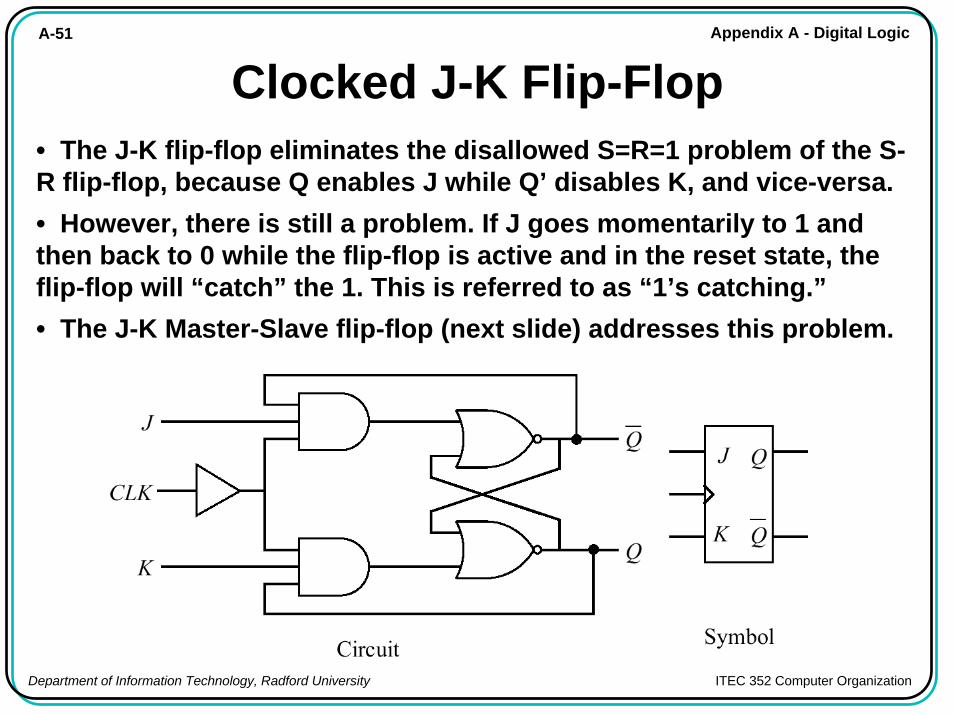
A-51 Appendix A - Digital Logic
Department of Information Technology, Radford University ITEC 352 Computer Organization
Clocked J-K Flip-Flop• The J-K flip-flop eliminates the disallowed S=R=1 problem of the S-R flip-flop, because Q enables J while Q’ disables K, and vice-versa.• However, there is still a problem. If J goes momentarily to 1 and then back to 0 while the flip-flop is active and in the reset state, the flip-flop will “catch” the 1. This is referred to as “1’s catching.”• The J-K Master-Slave flip-flop (next slide) addresses this problem.
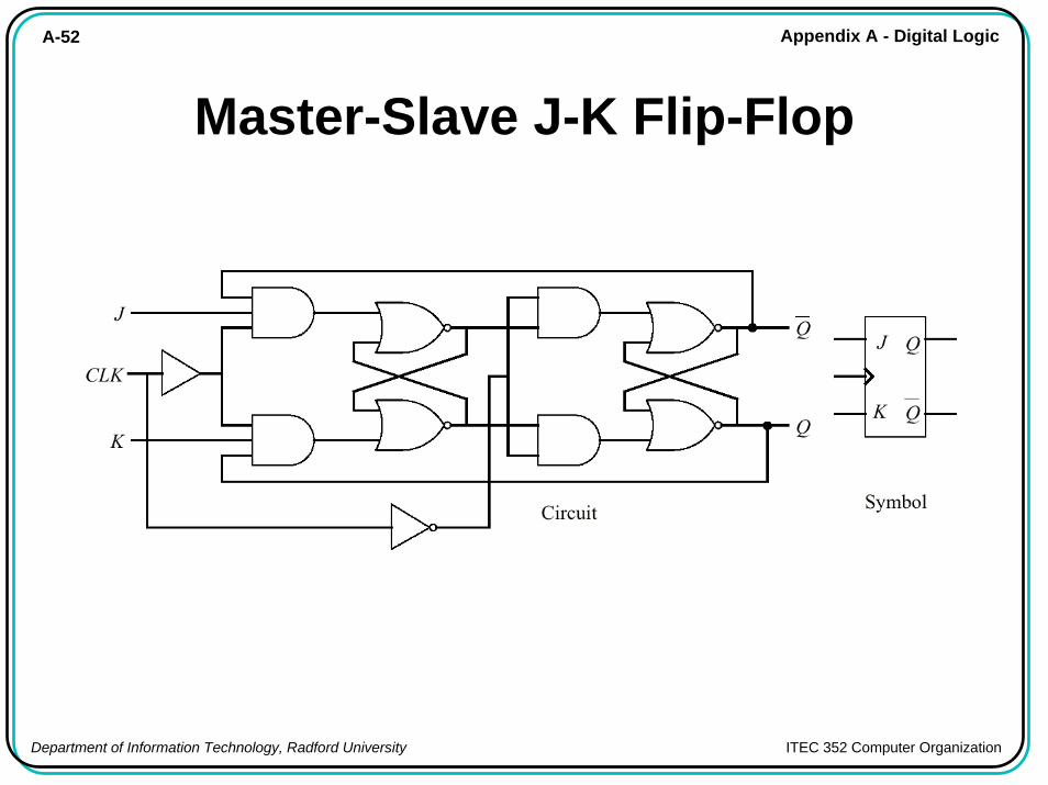
A-52 Appendix A - Digital Logic
Department of Information Technology, Radford University ITEC 352 Computer Organization
Master-Slave J-K Flip-Flop
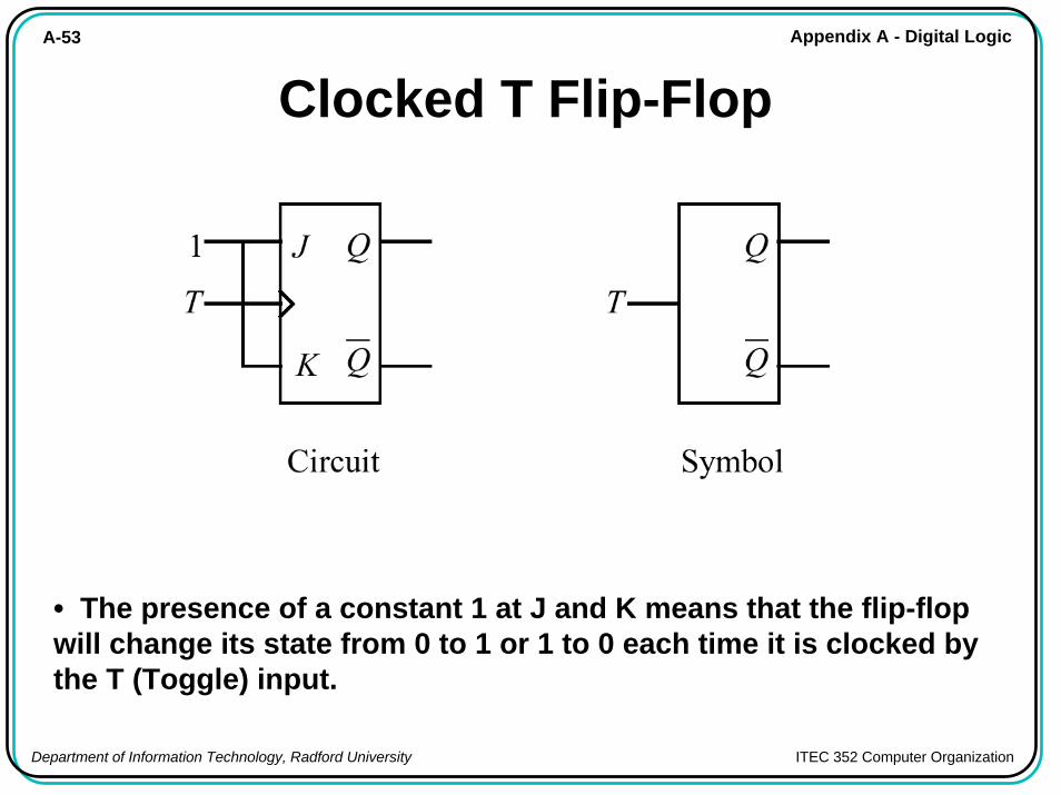
A-53 Appendix A - Digital Logic
Department of Information Technology, Radford University ITEC 352 Computer Organization
Clocked T Flip-Flop
• The presence of a constant 1 at J and K means that the flip-flop will change its state from 0 to 1 or 1 to 0 each time it is clocked by the T (Toggle) input.
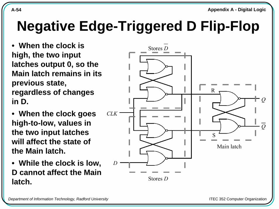
A-54 Appendix A - Digital Logic
Department of Information Technology, Radford University ITEC 352 Computer Organization
Negative Edge-Triggered D Flip-Flop• When the clock is high, the two input latches output 0, so the Main latch remains in its previous state, regardless of changes in D.• When the clock goes high-to-low, values in the two input latches will affect the state of the Main latch.• While the clock is low, D cannot affect the Main latch.
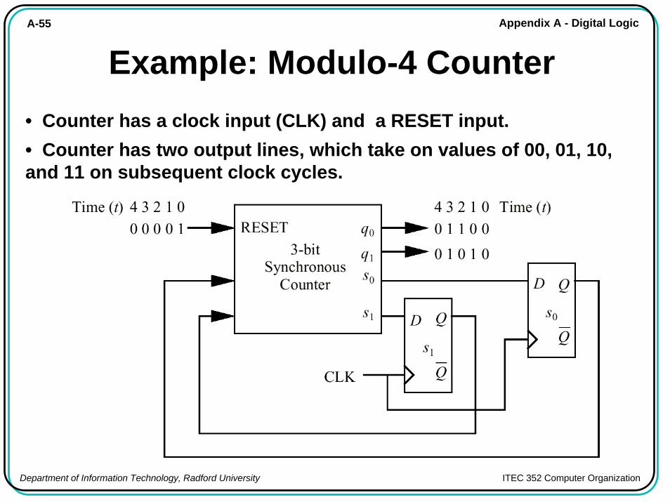
A-55 Appendix A - Digital Logic
Department of Information Technology, Radford University ITEC 352 Computer Organization
Example: Modulo-4 Counter• Counter has a clock input (CLK) and a RESET input.• Counter has two output lines, which take on values of 00, 01, 10, and 11 on subsequent clock cycles.
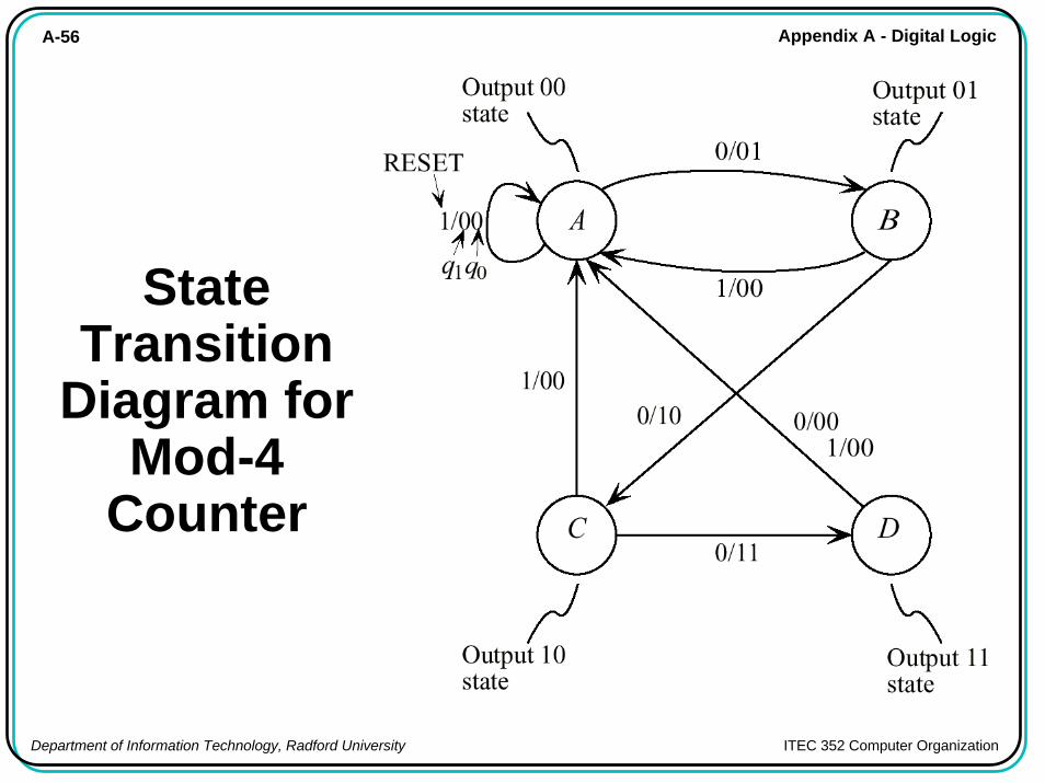
A-56 Appendix A - Digital Logic
Department of Information Technology, Radford University ITEC 352 Computer Organization
State Transition
Diagram for Mod-4
Counter
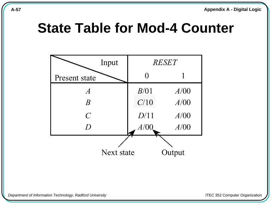
A-57 Appendix A - Digital Logic
Department of Information Technology, Radford University ITEC 352 Computer Organization
State Table for Mod-4 Counter
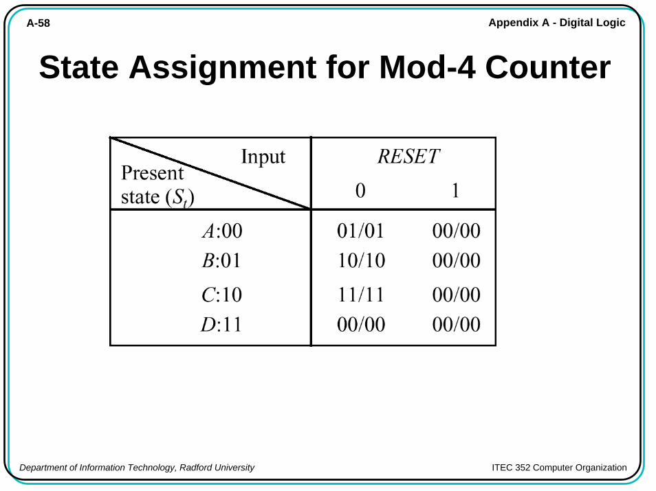
A-58 Appendix A - Digital Logic
Department of Information Technology, Radford University ITEC 352 Computer Organization
State Assignment for Mod-4 Counter
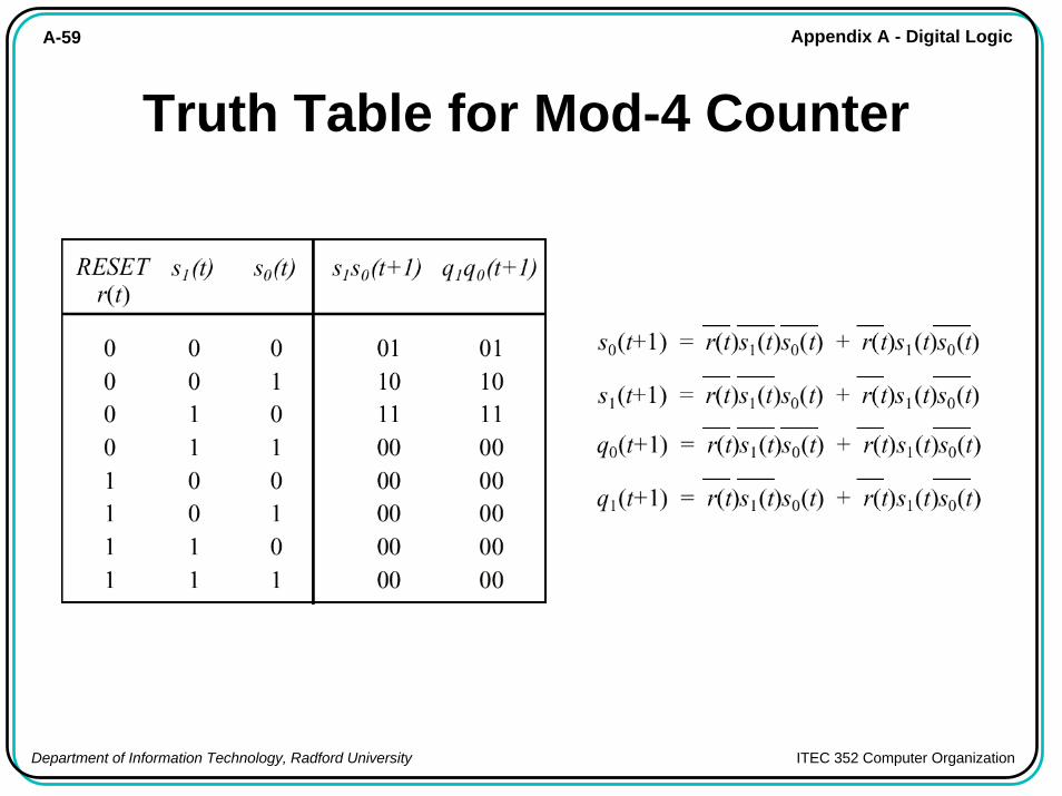
A-59 Appendix A - Digital Logic
Department of Information Technology, Radford University ITEC 352 Computer Organization
Truth Table for Mod-4 Counter
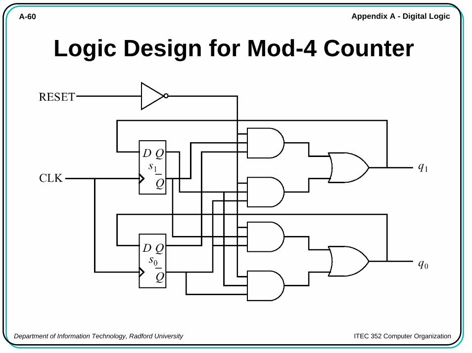
A-60 Appendix A - Digital Logic
Department of Information Technology, Radford University ITEC 352 Computer Organization
Logic Design for Mod-4 Counter
A-61 Appendix A - Digital Logic
Department of Information Technology, Radford University ITEC 352 Computer Organization
Example: A Sequence Detector
• Example: Design a machine that outputs a 1 when exactly two of the last three inputs are 1.• e.g. input sequence of 011011100 produces an output sequence of 001111010.• Assume input is a 1-bit serial line.• Use D flip-flops and 8-to-1 Multiplexers.• Start by constructing a state transition diagram (next slide).
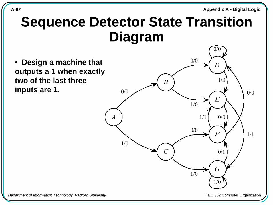
A-62 Appendix A - Digital Logic
Department of Information Technology, Radford University ITEC 352 Computer Organization
Sequence Detector State Transition Diagram
• Design a machine that outputs a 1 when exactly two of the last three inputs are 1.
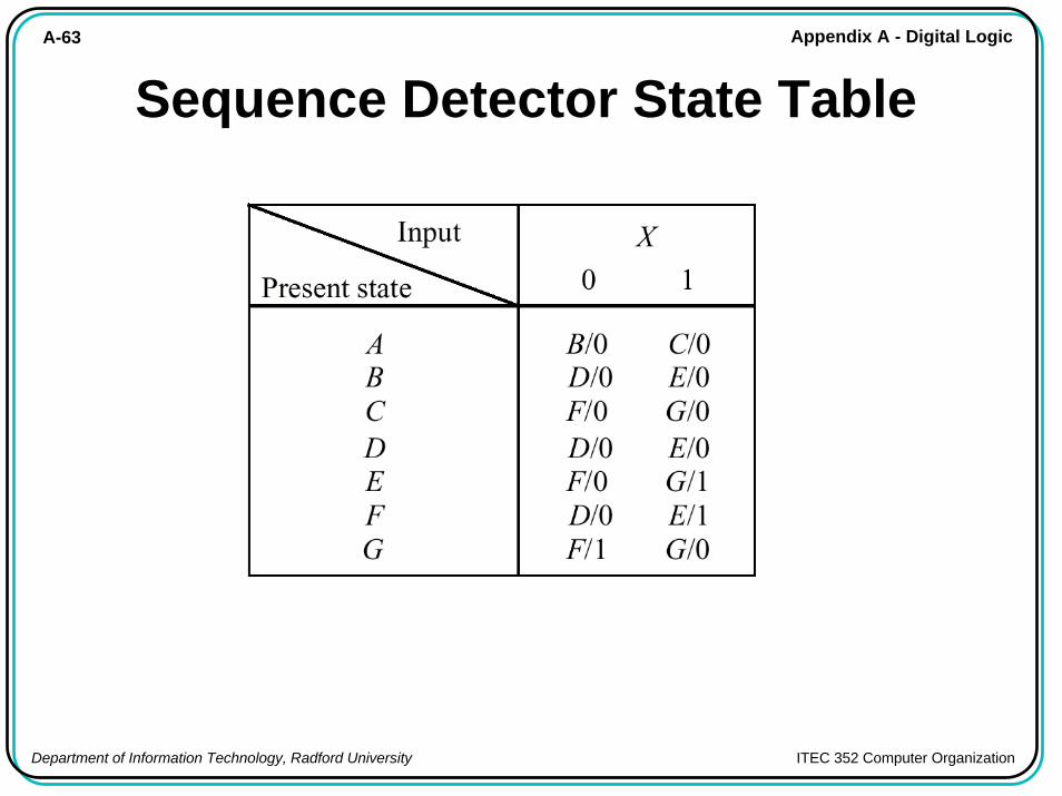
A-63 Appendix A - Digital Logic
Department of Information Technology, Radford University ITEC 352 Computer Organization
Sequence Detector State Table
A-64 Appendix A - Digital Logic
Department of Information Technology, Radford University ITEC 352 Computer Organization
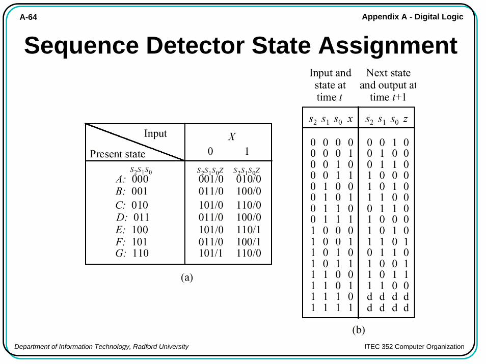
Sequence Detector State Assignment
A-65 Appendix A - Digital Logic
Department of Information Technology, Radford University ITEC 352 Computer Organization
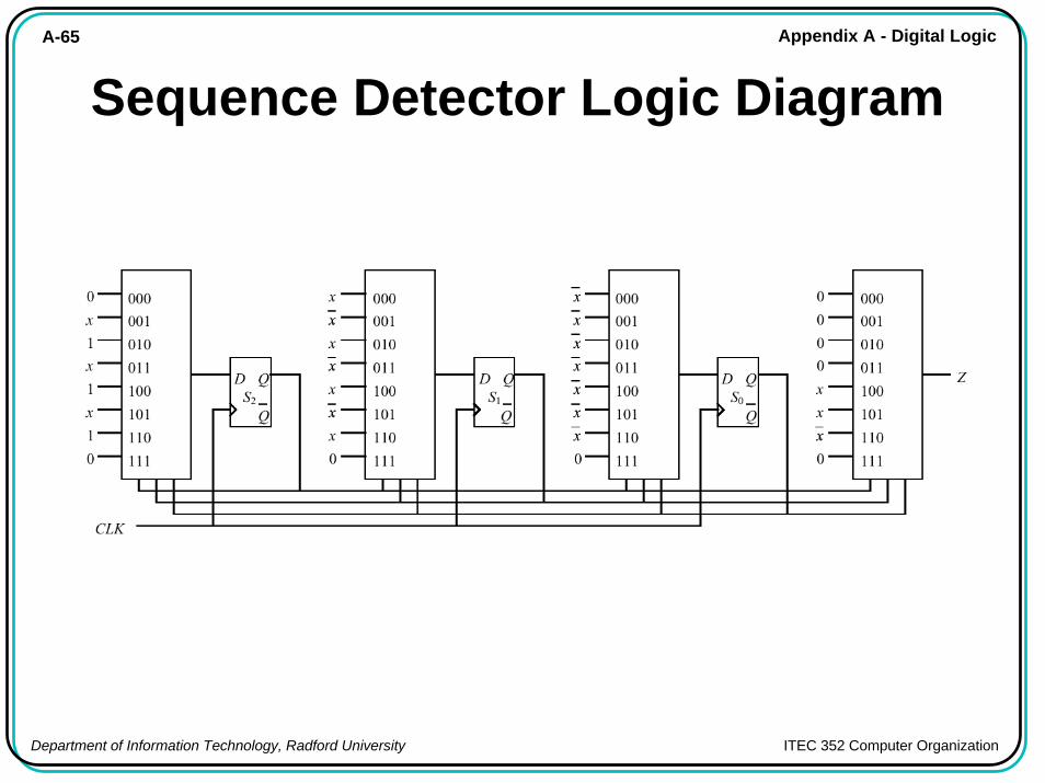
Sequence Detector Logic Diagram
A-66 Appendix A - Digital Logic
Department of Information Technology, Radford University ITEC 352 Computer Organization
Example: A Vending MachineController
• Example: Design a finite state machine for a vending machine controller that accepts nickels (5 cents each), dimes (10 cents each), and quarters (25 cents each). When the value of the money inserted equals or exceeds twenty cents, the machine vends the item and returns change if any, and waits for next transaction.• Implement with PLA and D flip-flops.
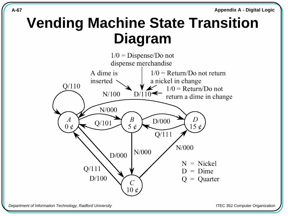
A-67 Appendix A - Digital Logic
Department of Information Technology, Radford University ITEC 352 Computer Organization
Vending Machine State TransitionDiagram
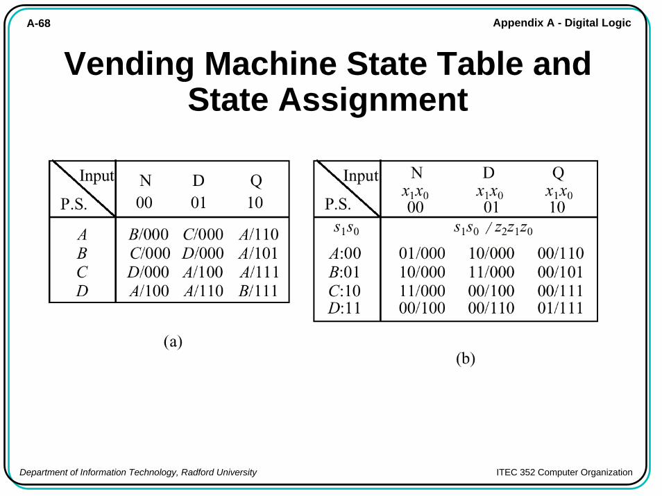
A-68 Appendix A - Digital Logic
Department of Information Technology, Radford University ITEC 352 Computer Organization
Vending Machine State Table and State Assignment
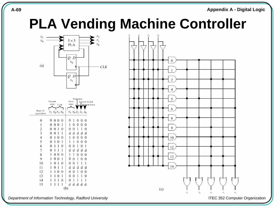
A-69 Appendix A - Digital Logic
Department of Information Technology, Radford University ITEC 352 Computer Organization
PLA Vending Machine Controller
A-70 Appendix A - Digital Logic
Department of Information Technology, Radford University ITEC 352 Computer Organization
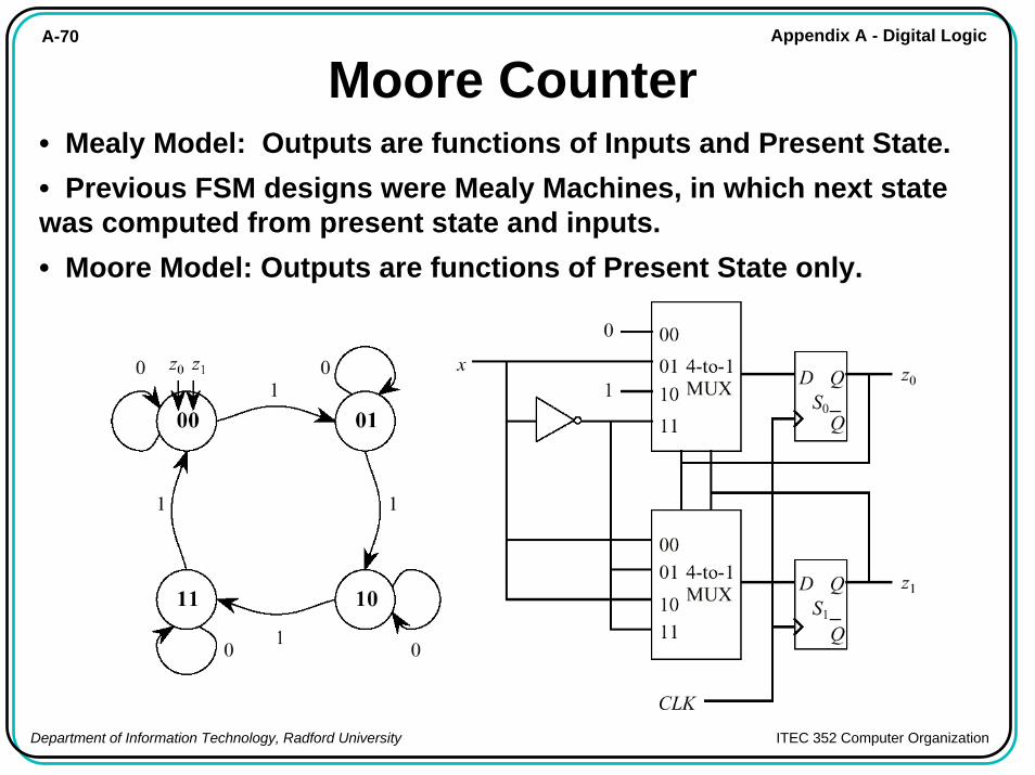
Moore Counter• Mealy Model: Outputs are functions of Inputs and Present State.• Previous FSM designs were Mealy Machines, in which next state was computed from present state and inputs.• Moore Model: Outputs are functions of Present State only.
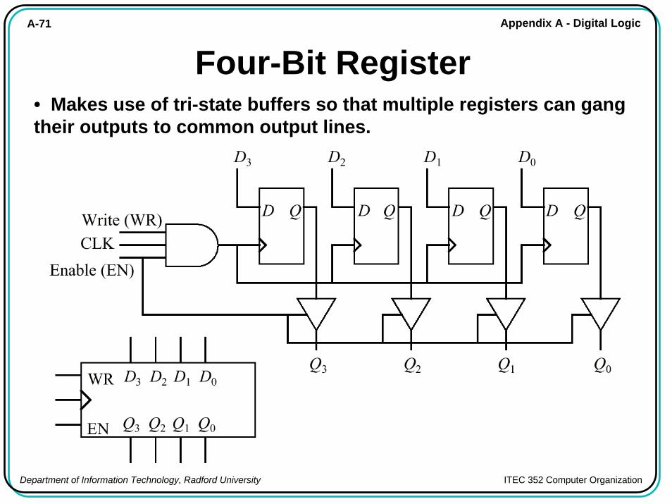
A-71 Appendix A - Digital Logic
Department of Information Technology, Radford University ITEC 352 Computer Organization
Four-Bit Register• Makes use of tri-state buffers so that multiple registers can gang their outputs to common output lines.
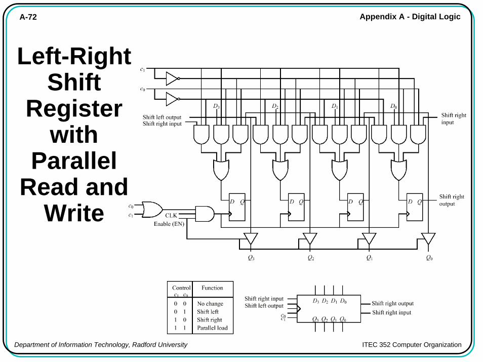
A-72 Appendix A - Digital Logic
Department of Information Technology, Radford University ITEC 352 Computer Organization
Left-Right Shift
Register with
Parallel Read and
Write
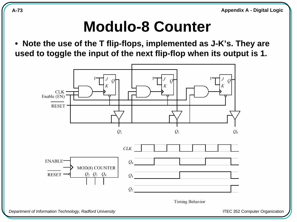
A-73 Appendix A - Digital Logic
Department of Information Technology, Radford University ITEC 352 Computer Organization
Modulo-8 Counter• Note the use of the T flip-flops, implemented as J-K’s. They are used to toggle the input of the next flip-flop when its output is 1.