Embed Size (px)
Citation preview
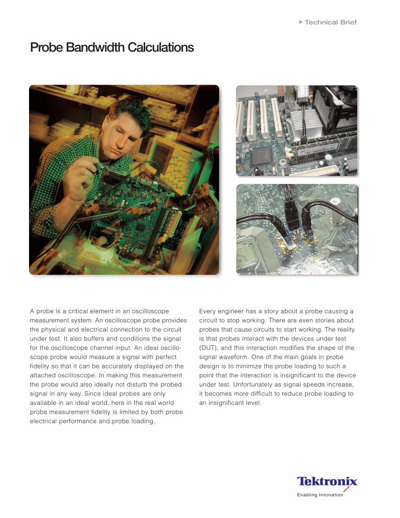
A probe is a critical element in an oscilloscopemeasurement system. An oscilloscope probe providesthe physical and electrical connection to the circuitunder test. It also buffers and conditions the signalfor the oscilloscope channel input. An ideal oscillo-scope probe would measure a signal with perfectfidelity so that it can be accurately displayed on theattached oscilloscope. In making this measurementthe probe would also ideally not disturb the probedsignal in any way. Since ideal probes are only available in an ideal world, here in the real worldprobe measurement fidelity is limited by both probeelectrical performance and probe loading.
Every engineer has a story about a probe causing acircuit to stop working. There are even stories aboutprobes that cause circuits to start working. The realityis that probes interact with the devices under test(DUT), and this interaction modifies the shape of thesignal waveform. One of the main goals in probedesign is to minimize the probe loading to such apoint that the interaction is insignificant to the deviceunder test. Unfortunately as signal speeds increase,it becomes more difficult to reduce probe loading toan insignificant level.
Technical Brief
Probe Bandwidth Calculations
Probe Bandwidth CalculationsTechnical Brief
2 www.tektronix.com/accessories22
Increasing signal speed for digital communicationshas placed new demands on probe electrical perform-ance and loading. High speed signal probing requiresan oscilloscope probe to measure signals in a trans-mission line environment. The effect of probe loadingin a transmission line environment requires a morecomplex treatment than the simple discrete probeload models once commonly used. Probe loadingeffects in a distributed circuit environment have alsoled a probe vendor to introduce a new approach toboth probe measurement and probe specification.Because this new approach has created some confusion in the probe market, this paper will examinethis new approach and compare it with the more traditional, accepted approach.
Probe Loading
Historically, oscilloscope probes have been describedusing discrete models. A typical discrete model, asshown in Figure 1, describes the probe loading as DCresistance and an input capacitance.
This is a valid method when the signal speeds areslow. Electrical signals will propagate down a trans-mission line with a propagation velocity that depends
on the physical properties of the material around thetransmission line. For a microstrip transmission line onFR-4 circuit board material, the propagation velocity isabout 150 ps/inch, which is about half the speed oflight. For a signal rise time of 500 ps, the length oftransmission line over which the rise time variation ofthe signal can be observed is about three inches(electrical length = signal rise time/propagation velocity). A conservative guideline that can be appliedis that an interconnect can be expected to showtransmission line effects for interconnects longer than 1/6th the length over which the signal variationpropagates (0.5 inch for the microstrip transmissionline example)*1. As long as the physical characteristicsof the circuit are smaller than this 1/6th of a propagationlength, a discrete model can be used. However aselectrical interconnects get faster, this becomes muchmore of an issue. A 100 ps rise time signal will have a 0.66 inch propagation length in FR-4. Features larger than 0.11 inches will start to show transmission line effects.
Oscilloscope probes are now being described withdistributed models, as shown in Figure 2. These modelshelp to take into account transmission line effects.
2
Figure 1. Discrete Model of Probe Loading. Figure 2. Distributed Model of Probe Loading.
*1"TekConnect™ Probes: Signal Fidelity Issues and Modeling", Tektronix, Inc.
Probe Bandwidth CalculationsTechnical Brief
3www.tektronix.com/accessories
Probe loading can be more accurately characterizedby its input impedance over the frequency range ofthe probe. Figure 3 shows the input impedance variation with frequency of a high performance differ-ential probe. The use of input impedance is a straight-forward way to model complex interactions betweenresistance, capacitance and inductance over frequency.This characterization method allows probe users to gauge the impact of the probe loading at specific frequencies.
Oscilloscope Probing Philosophy
Oscilloscope probes have a very different usagemodel when compared to oscilloscopes. Today’s highbandwidth oscilloscopes all have 50Ω terminations oneach channel. The oscilloscope is meant to be usedas an end-of-line receiver that expects to see a signalcoming from a 50Ω source. An oscilloscope probe isintended to be connected to a device under test thatis, presumably, already source and receiver terminated.These probes are usually designed to have a highinput impedance so that the probe affects the deviceunder test as little as possible.
There are two schools of thought on what an oscilloscopeprobe should actually display on an oscilloscope.Tektronix subscribes to the philosophy that a probeshould measure the unloaded, or original, signal.Agilent subscribes to a different philosophy that saysa probe should measure the loaded signal. Whatexactly does this mean? First you have to understandhow probe bandwidth is characterized.
The through response, or transfer function, of a probeis characterized as VOUT / VIN where VIN is the input tothe probe and the VOUT is the output of the probe. Theratio describes the gain of the probe amplifier andcan be written as VOUT (f)/VIN(f) because this gain canchange with frequency. The bandwidth of the probe isdefined as the frequency at which the transfer functionof the probe is down to 0.707 (3dB) of its low frequency
value. This is an industry standard definition of bandwidth. The difference in implementation method-ology between Tektronix and Agilent concerns the definition of the reference signal, VIN. Introducing theprobe into that well controlled environment can causethat environment to change. Tektronix and Agilentaccount for that change in different ways.
Throughout the years, 50Ω environments have beenthe standard for generation and transmission of highspeed signals. Consequently, oscilloscope probeshave been generally characterized using a terminated50Ω signal generator. The response of a test signalgenerator is calibrated to be as flat as possible overthe frequency range of interest. Tektronix characterizesthis flat source (VSOURCE) and calls it VIN. The probe response is then designed to be as flat as possible throughout its frequency range in this clean50Ω environment. This method of characterizingprobes has an inherent effect of compensating for the probe loading. A probe of this type displays theoriginal unloaded signal on the oscilloscope. This isthe signal the device under test would see before theprobe is attached.
Figure 3. Differential Input Impedance of Tektronix P7380 with ShortFlex Small Resistor Flex Tip-Clip™ Assembly.
Probe Bandwidth CalculationsTechnical Brief
4 www.tektronix.com/accessories
Agilent takes the position that the loading of the probehas an impact on the measured signal such thatVSOURCE ≠ VIN. They assert that the probe’s frequencydependent loading has to be measured and factoredinto the calibration to accurately derive the bandwidthof the probe. A probe that has been characterizedwith this method gives a bandwidth and proberesponse that includes the loading of the probe in a50Ω environment. This probe does not attempt to compensate for the loading, but in fact includes the loading. An Agilent probe displays on the oscilloscope screen the original signal as it has been loaded by the probe.
If a probe existed that had no loading, both philosophieswould converge and you would see no differencebetween the probes. Since probe loading does exist,the difference in measurement philosophy has animpact on both the waveform displayed by the probeand the specifications of the probe bandwidth.
To better explain the difference in philosophies, let us look at a simplified example. Suppose you have aperfect 1VDC signal that you want to measure. Whenyou measure this signal with a probe, you expect theprobe to measure 1VDC. If probe loading caused thesignal level to drop to 0.95V, would you want theprobe to read 1VDC or 0.95VDC? The Tektronix philosophy is that you want to see a 1V signal.Agilent’s philosophy is that you want to see the 0.95V signal.
This example can be taken one step further. Supposeyou want to measure a perfect AC sinusoidal 1Vppsignal. This signal can be swept from a few hertz togigahertz frequencies and still have a perfect 1Vppsignal level. As the signal source is swept through itsfrequency range, should the probe output change withfrequency due to its changing load profile or shouldthe output of the probe read 1Vpp throughout the
majority of its frequency range? This is a simplifiedexample, but it clearly illustrates the differences inprobing philosophy.
Tektronix believes that it is more useful for probeusers to know what is happening inside their circuitswhen the probe is not attached. The remainder of thispaper examines in greater detail the effect of Agilent’sprobing philosophy and why Tektronix supports thetraditional bandwidth measurement technique.
How Probe Bandwidth is Measured
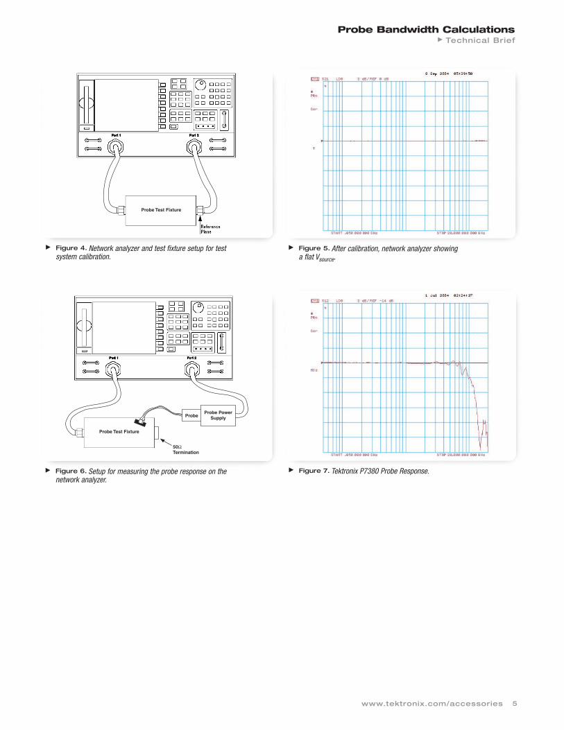
Tektronix designs the probe response to be as flat aspossible throughout its frequency range. This flatnessis tested with a Network Analyzer that has been calibrated along with a probe test fixture to be a flatsource out to 20 GHz, as shown in Figures 4 and 5.Network analyzers typically have special high frequency coaxial connectors, so a special probe calibration test fixture is used to connect the probe tothe network analyzer. The network analyzer is thencalibrated to take out any frequency effects of thecables and the test fixture. This method insures therepeatability of the measurement because there canbe slight differences in cables and fixtures betweentest stations. This flat system is what Tektronix definesas VSOURCE or VIN.
The probe is then connected to the test fixture, asshown in Figure 6, and the response of the probe ismeasured, as shown in Figure 7.
Probes have components that can be used to adjusttheir frequency response. These components can beactively adjusted to calibrate the probe in real timeand make the response as flat as possible throughoutits frequency range. One advantage of this method isthat the frequency dependant loading of the probe isautomatically compensated in the process.
Probe Bandwidth CalculationsTechnical Brief
5www.tektronix.com/accessories
Figure 4. Network analyzer and test fixture setup for test system calibration.
Probe Test Fixture
Figure 5. After calibration, network analyzer showing a flat Vsource.
Figure 6. Setup for measuring the probe response on the network analyzer.
Figure 7. Tektronix P7380 Probe Response.
Probe Test Fixture
ProbeProbe Power
Supply
50ΩTermination
Probe Bandwidth CalculationsTechnical Brief
6 www.tektronix.com/accessories
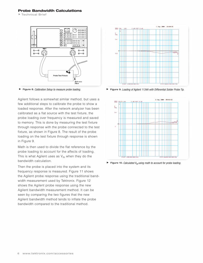
Agilent follows a somewhat similar method, but uses afew additional steps to calibrate the probe to show aloaded response. After the network analyzer has beencalibrated as a flat source with the test fixture, theprobe loading over frequency is measured and savedto memory. This is done by measuring the test fixturethrough response with the probe connected to the testfixture, as shown in Figure 8. The result of the probeloading on the test fixture through response is shownin Figure 9.
Math is then used to divide the flat reference by theprobe loading to account for the affects of loading.This is what Agilent uses as VIN when they do thebandwidth calculation.
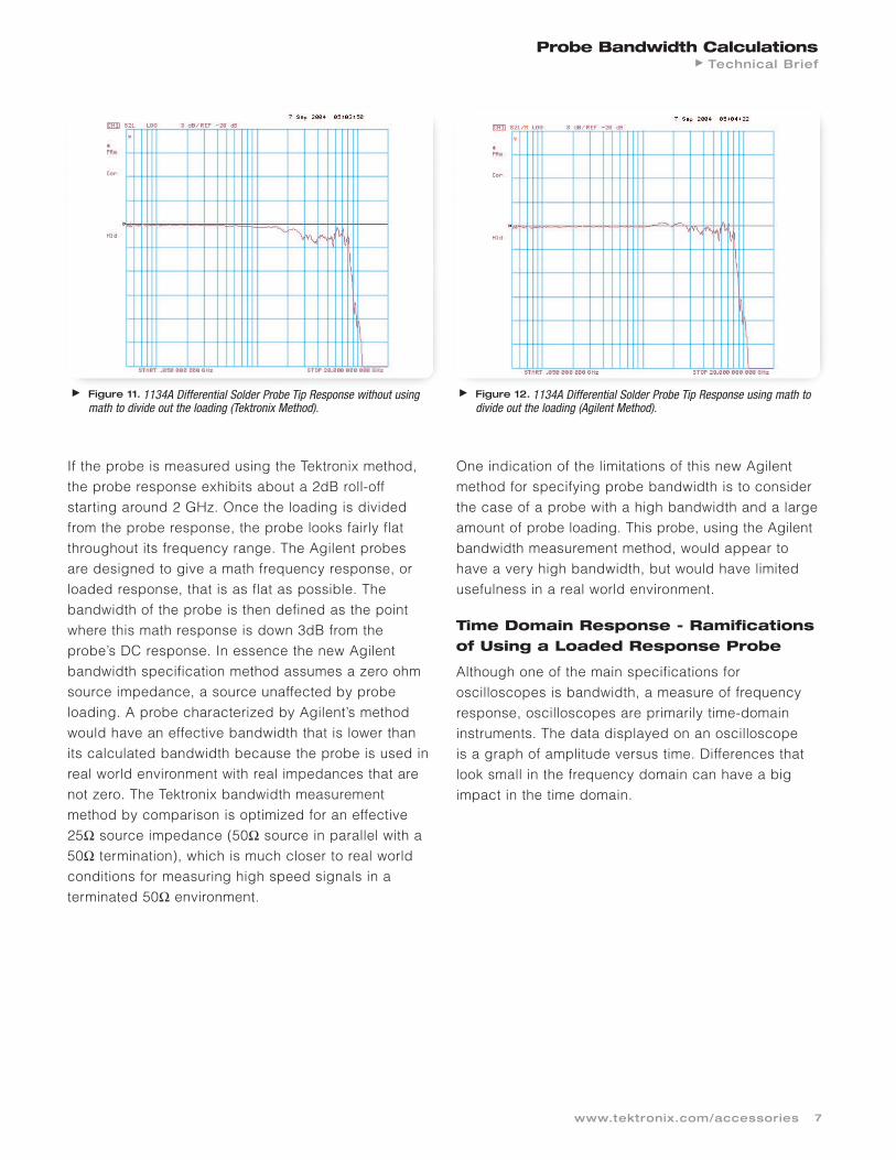
Then the probe is placed into the system and its frequency response is measured. Figure 11 shows the Agilent probe response using the traditional band-width measurement used by Tektronix. Figure 12shows the Agilent probe response using the newAgilent bandwidth measurement method. It can beseen by comparing the two figures that the newAgilent bandwidth method tends to inflate the probebandwidth compared to the traditional method.
Figure 8. Calibration Setup to measure probe loading. Figure 9. Loading of Agilent 1134A with Differential Solder Probe Tip.
Figure 10. Calculated VIN using math to account for probe loading.
Probe Test Fixture
Probe Bandwidth CalculationsTechnical Brief
7www.tektronix.com/accessories
If the probe is measured using the Tektronix method,the probe response exhibits about a 2dB roll-off starting around 2 GHz. Once the loading is dividedfrom the probe response, the probe looks fairly flatthroughout its frequency range. The Agilent probesare designed to give a math frequency response, orloaded response, that is as flat as possible. Thebandwidth of the probe is then defined as the pointwhere this math response is down 3dB from theprobe’s DC response. In essence the new Agilentbandwidth specification method assumes a zero ohmsource impedance, a source unaffected by probeloading. A probe characterized by Agilent’s methodwould have an effective bandwidth that is lower thanits calculated bandwidth because the probe is used inreal world environment with real impedances that arenot zero. The Tektronix bandwidth measurementmethod by comparison is optimized for an effective25Ω source impedance (50Ω source in parallel with a50Ω termination), which is much closer to real worldconditions for measuring high speed signals in a terminated 50Ω environment.
One indication of the limitations of this new Agilentmethod for specifying probe bandwidth is to considerthe case of a probe with a high bandwidth and a largeamount of probe loading. This probe, using the Agilentbandwidth measurement method, would appear tohave a very high bandwidth, but would have limitedusefulness in a real world environment.
Time Domain Response - Ramificationsof Using a Loaded Response Probe
Although one of the main specifications for oscilloscopes is bandwidth, a measure of frequencyresponse, oscilloscopes are primarily time-domaininstruments. The data displayed on an oscilloscope is a graph of amplitude versus time. Differences thatlook small in the frequency domain can have a bigimpact in the time domain.
Figure 11. 1134A Differential Solder Probe Tip Response without usingmath to divide out the loading (Tektronix Method).
Figure 12. 1134A Differential Solder Probe Tip Response using math todivide out the loading (Agilent Method).
Probe Bandwidth CalculationsTechnical Brief
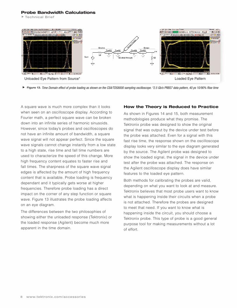
A square wave is much more complex than it lookswhen seen on an oscilloscope display. According toFourier math, a perfect square wave can be brokendown into an infinite series of harmonic sinusoids.However, since today’s probes and oscilloscopes donot have an infinite amount of bandwidth, a squarewave signal will not appear perfect. Since the squarewave signals cannot change instantly from a low stateto a high state, rise time and fall time numbers areused to characterize the speed of this change. Morehigh frequency content equates to faster rise and fall times. The sharpness of the square wave signaledges is affected by the amount of high frequencycontent that is available. Probe loading is frequencydependant and it typically gets worse at higher frequencies. Therefore probe loading has a directimpact on the corner of any step function or squarewave. Figure 13 illustrates the probe loading affectson an eye diagram.
The differences between the two philosophies ofshowing either the unloaded response (Tektronix) orthe loaded response (Agilent) become much moreapparent in the time domain.
How the Theory is Reduced to Practice
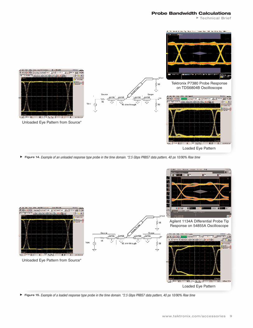
As shown in Figures 14 and 15, both measurementmethodologies produce what they promise. TheTektronix probe was designed to show the original signal that was output by the device under test beforethe probe was attached. Even for a signal with thisfast rise time, the response shown on the oscilloscope display looks very similar to the eye diagram generatedby the source. The Agilent probe was designed toshow the loaded signal, the signal in the device undertest after the probe was attached. The response onthe Agilent oscilloscope display does have similar features to the loaded eye pattern.
Both methods for calibrating the probes are valid,depending on what you want to look at and measure.Tektronix believes that most probe users want to knowwhat is happening inside their circuits when a probeis not attached. Therefore the probes are designed to meet that need. If you want to know what is happening inside the circuit, you should choose aTektronix probe. This type of probe is a good generalpurpose tool for making measurements without a lot of effort.
8 www.tektronix.com/accessories
Figure 13. Time Domain effect of probe loading as shown on the CSA/TDS8000 sampling oscilloscope. *2.5 Gb/s PRBS7 data pattern, 40 ps 10/90% Rise time
Unloaded Eye Pattern from Source* Loaded Eye Pattern
Probe Bandwidth CalculationsTechnical Brief
9www.tektronix.com/accessories
Figure 14. Example of an unloaded response type probe in the time domain. *2.5 Gbps PRBS7 data pattern, 40 ps 10/90% Rise time
Unloaded Eye Pattern from Source*
Loaded Eye Pattern
Tektronix P7380 Probe Response on TDS6804B Oscilloscope
Figure 15. Example of a loaded response type probe in the time domain. *2.5 Gbps PRBS7 data pattern, 40 ps 10/90% Rise time
Unloaded Eye Pattern from Source*
Loaded Eye Pattern
Agilent 1134A Differential Probe TipResponse on 54855A Oscilloscope
Probe Bandwidth CalculationsTechnical Brief
If you want to see how the probe is affecting your circuit, you should consider choosing an Agilent probe.For example, this is useful if the circuit can be modeledand simulated. The probe loading can be added tothe model and the output of the simulation can bechecked with the output of probe and oscilloscope. A Tektronix probe can be used for this type of measurement, but it requires that the device undertest be terminated into an oscilloscope channel, typically through a coax cable. This type of connectionis not always available on circuit boards.
An Agilent probe is good in a few specific applications,but it does not work very well as a general purposetool. The probe will not give you the data you are looking for without a lot of auxiliary calculation andextra time because the loading of the probe is alwaysincluded in the data. This type of probe is not a good general purpose tool because it adds an extralayer of complexity.
Engineers know what they expect to see when theymeasure their circuits and they use probes to verifythat everything is working as designed. The Agilentprobe will only show the system performance as it isaffected by the probe loading. Engineers then have to decide if what they are seeing is due to their system or just part of the effect of probe loading. It ispossible to take the data and work backwards to findthe original signal, but this process is difficult andtime consuming. Agilent has no automated oscillo-scope routine that will perform this step. It must bedone for every single waveform that is measured. Ifthis step is omitted, then the data that is recorded issuspect. This phenomenon can become even more ofa issue if engineers want to use one of the vast arrayof applications that are available on oscilloscopes.
All of theses applications use the oscilloscope data to perform their analysis. If the raw probe data isused, the applications may give false passes or failsbecause of the extra effects from the probe that arenot there in the original signal.
Agilent has an application note that describes in moredetail methods that can be used to take the output oftheir probe and work backwards to display the originalsignal. Agilent sampling oscilloscopes have a normal-ization feature that can be used to calibrate out testfixture features when making time-domain reflectometer(TDR) measurements. This same normalization featurecan be used to account for the probe loading and helpsthe probe display the original signal. The drawback tothis method is that the source needs to be well char-acterized with the probe loading in place before thenormalization can occur. In many instances, the probeuser’s final goal is to characterize their own signal.Why go through all the trouble to fully characterizetheir signal so that they can go back and measure itagain with the probe? Agilent’s real time oscilloscopesdo not have this normalization feature. Their solutionto this problem is to add a probe compensation circuitto the source using discrete components. While thisdoes produce the desired effect, it is an impracticalsolution for engineers testing their own circuits. Whygo through all the trouble to back out the original signal from the Agilent probe when a Tektronix probedoes this directly?
Another drawback of an Agilent probe is that it cannot be reliably used for mask testing. As can be seen in the pictures, probe loading can have a significant impact on the front corner of high speeddigital signals. This could cause a signal to artificiallyfail or pass a mask test because the probe loading ispart of the response.
10 www.tektronix.com/accessories
Probe Bandwidth CalculationsTechnical Brief
Mask testing is an important tool for high speed serialdata testing. Most serial data standards specifymasks that may be used to validate data streams tomake sure they comply to the standards. The masksare typically designed to be used with an end-of-linereceiver, like a terminated 50Ω oscilloscope channelor an SMA-input probe like the P7380SMA. End-of-linereceivers do not have to deal with the issues of probeloading. The signal quality that reaches the receiverdepends mainly on the quality of the transmissionlines and the 50Ω termination. The masks define thelimits of a serial data stream in its intended environment,which does not include external factors like probeloading. Sometimes it is not possible to gain accessto a serial data stream to pipe it directly into an oscilloscope. An example of this situation would betwo chips on the same board that have a high speedserial connection between them. The only way to gain access to the data stream would be to use anoscilloscope probe.
A Tektronix probe can be used for mask testingbecause the probe is designed to reproduce the signal as it was in its original environment. On theother hand, an Agilent probe displays a signal thatincludes the probe loading and may not meet the criteria to make a valid mask test. A circuit that isdesigned to pass a mask test with an Agilent probe may experience problems when the probe is not connected to the system, because it passed the testin a non-valid environment. An Agilent probe may beused to make compliance tests if special modifiedmasks are used, but standard masks as specified bythe standard committees cannot be used.
The Agilent probe’s rise time measurements may alsobe invalid because the probe’s loading affects thefront corner of any step response. The proberesponse that is displayed on the oscilloscope screenincludes the loading. Oscilloscope measurementalgorithms are typically designed to look for a 10-90%point to make its measurement. Distortion in the frontcorner may change the wave shape enough that the90% point is significantly different and measuresincorrectly. 20-80% rise time measurements experienceless of an impact from front corner distortionsbecause the measurement takes place farther fromthe corner.
Conclusion
An oscilloscope probe is a tool used by engineers toquickly make measurements and help get products tomarket. The enormous increase in signal speeds overthe past few years has introduced complexities inprobing that probe users need to know about andaccount for. In the past, all oscilloscope probedesigners subscribed to the same philosophy. Theintroduction of Agilent’s loaded response type probehas given probe users an extra tool, but it has alsocaused some confusion.
Care must be taken to understand how a probe willinteract with a DUT, no matter which probe type isused. Agilent probes might be good tools for a smallset of applications, but are not well suited for general purpose probing tasks like DUT characterization, validation, and mask testing because they requireextra calculation to extract the probe loading. In contrast, Tektronix probes are good tools for general purpose probing tasks because theyendeavor to directly show the original, unloaded signal.
11www.tektronix.com/accessories

Contact Tektronix:
ASEAN / Australasia / Pakistan (65) 6356 3900
Austria +41 52 675 3777
Balkan, Israel, South Africa and other ISE Countries +41 52 675 3777
Belgium 07 81 60166
Brazil & South America 55 (11) 3741-8360
Canada 1 (800) 661-5625
Central Europe & Greece +41 52 675 3777
Central East Europe, Ukraine and Baltics +41 52 675 3777
Denmark 80 88 1401
Finland +41 52 675 3777
France & North Africa +33 (0) 1 69 81 81
Germany +49 (221) 94 77 400
Hong Kong (852) 2585-6688
India (91) 80-22275577
Italy +39 (02) 25086 1
Japan 81 (3) 6714-3010
Luxembourg +44 (0) 1344 392400
Mexico, Central America & Caribbean 52 (55) 56666-333
Middle East, Asia and North Africa +41 52 675 3777
The Netherlands 090 02 021797
Norway 800 16098
People’s Republic of China 86 (10) 6235 1230
Poland +41 52 675 3777
Portugal 80 08 12370
Republic of Korea 82 (2) 528-5299
Russia, CIS & The Baltics 7 095 775 1064
South Africa +27 11 254 8360
Spain (+34) 901 988 054
Sweden 020 08 80371
Switzerland +41 52 675 3777
Taiwan 886 (2) 2722-9622
United Kingdom & Eire +44 (0) 1344 392400
USA 1 (800) 426-2200
USA (Export Sales) 1 (503) 627-1916
For other areas contact Tektronix, Inc. at: 1 (503) 627-7111
Updated November 3, 2004
For Further InformationTektronix maintains a comprehensive, constantly expanding collection ofapplication notes, technical briefs and other resources to help engineersworking on the cutting edge of technology. Please visit www.tektronix.com
Copyright © 2004, Tektronix, Inc. All rights reserved. Tektronix products are covered by U.S. and foreignpatents, issued and pending. Information in this publication supersedes that in all previously published material. Specification and price change privileges reserved. TEKTRONIX and TEK areregistered trademarks of Tektronix, Inc. All other trade names referenced are the service marks,trademarks or registered trademarks of their respective companies. 11/04 FLG/WOW 60W-18324-0
Sources:
"Z-Active™: A New High Performance ProbeArchitecture", Tektronix, Inc.
"ABC's of Probes", Tektronix, Inc.
"Side-by-Side Comparison of Agilent and TektronixProbing Measurements on High-Speed Signals", Agilent App Note 1491 Agilent Technologies, Inc.
"Time-Domain Response of Agilent InfiniiMax Probesand 54850 Series Infiniium Oscilloscopes", Agilent App Note 1461 Agilent Technologies, Inc.
User Manual: 1134A 7 GHz InfiniiMax Differential and Single-ended Probes (Publication Number 01134-97007), Agilent Technologies, Inc.