Embed Size (px)
Citation preview

PROBEWORKSTATION
A P P L I C A T I O N S
Failure analysis
Qualifying high к gate materials
Low-current transistor testing
Four-point probing
EBIC, EBAC, RCI, EBIV, EBIRCH, and Active
Potential Contrast analysis
Current Imaging
Characterization of advanced materials
and structures e.g. nanowires, ultra-thin
films
Nanoscale assembly and manipulation
PROBEWORKSTATION
The ProbeWorkstation is a powerful, dedicated
system for electrical characterization of semicon-
ductor devices and advanced materials in SEM
and FIB.
The optimal combination of our market-leading
nanomanipulation and probing products provide
you with a versatile, integrated solution for fail-
ure analysis and R&D applications requiring stable,
low-current measurements.
The system is optimized for electrical measure-
ments on semiconductor technologies down to
7 nm and beyond. It offers unsurpassed stabil-
ity, extreme precision, and the flexibility to allow
you to configure your setup to meet your specific
needs.
C O M P O N E N T S
Up to eight micromanipulators with
low-current measurement capability
Precision substage with three axes for
independent sample positioning
Shuttle load-lock platform
EBIC Characterization System
Advanced Probing Tools GUI:
An advanced software suite for maximum
probing efficiency - including the
following modules:
§ iProbe
§ Live Contact Tester
§ Tip 2 Tip Tester
§ Transistor Test
§ Safe Tip Approach
§ EBIC control
§ Current Imaging module
§ Keithley Remote access
§ Tip Cleaning
Electronics rack
Next generation technology has allowed us to dra-
matically reduce the size of our micromanipula-
tors. This innovation, coupled with our new Shuttle
platform, has enabled the creation of the world’s
smallest load-lock compatible probing system.
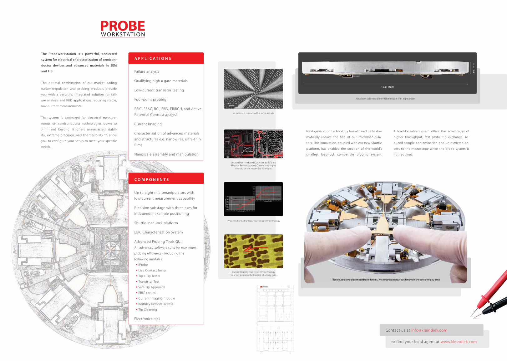
A load-lockable system offers the advantages of
higher throughput, fast probe tip exchange, re-
duced sample contamination and unrestricted ac-
cess to the microscope when the probe system is
not required.
Contact us at [email protected]
or find your local agent at www.kleindiek.com
1 2 3 4
menu
1 2 3 4
menu
1 2 3 4
menu
1 2 3 4
menu
InvertGain�1-100
10
1001
Cap.�(AC)
100p
100n1n10n
1µ
10p
Res.�(AC)
5k
50k
10k20k
2k
1k
Gain�10x
7
10
89
6
5
AC�Amp.
DC�Amp.Offset�coarse
- +
Offset�fine
- +
Power�On
EBIC
1 2 3 4
menu
1 2 3 4
menu
1 2 3 4
menu
1 2 3 4
menu
1 2 3 4
menu
Tip1 Tip2
Tip3 Tip4
Bulk
Tip5 Tip6
Tip7 Tip8
Bulk
0
I+12V+5V
Power
LCT
I-V curves from a transistor built on 22 nm technology
Current Imaging map on 22 nm technologyThe arrow indicates the location of a leaky gate...
Electron Beam Induced Current map (left) andElectron Beam Absorbed Current map (right)
overlaid on the respective SE images
m m
m
m
Actual size Side view of the Prober Shuttle with eight probes
The robust technology embedded in the MM4 micromanipulators allows for simple pre-positioning by hand The robust technology embedded in the MM4 micromanipulators allows for simple pre-positioning by hand
Six probes in contact with a 14 nm sample
n m

The Current Imaging system is used to generate current maps - similar to pico-current cAFM.
The APT wizard provides detailed, animated step by step instructions for a number of tasks.
Probe needles
§ Tungsten needles with tip radii down to 5 nm
§ Individually packaged in protective atmosphere and
ready for use without further processing
§ pre-bent tips available upon request
§ easy tip exchange outside the microscope
§ SEM and FIB load-lock compatibility – for fast cycle times and increased chamber cleanliness.
§ Simple integration into your existing SEM or FIB/SEM tool.
§ Streamlined, low-leakage triax cabling between 19” electronics rack and SEM flange
§ Software controlled signal switching matrix, no rewiring necessary
§ Completely nonmagnetic materials: compatible with any SEM/FIB (including “immersion lens” type columns)
§ Low profi le design allows for small working distances down to 2 mm - enabling low-kv imaging
§ Probing at FIB tilt for in-situ circuit edit applications
§ Compact, extremely stable design guarantees < nm/min drift: ready for nm and beyond
§ Live Contact Tester provides real time IV-traces: quickly optimize contact resistance
§ Integrated Scanning Probe Microscope: Current Imaging module can be used to scan a probe or the substage using well-defined current paths
§ Electrical Fault Isolation using EBIC, EBAC, EBIV, RCI, EBIRCH, etc. Easy inte-gration using the microscope ‘s auxiliary video input, EBIC image acquisition by SEM software.
§ Tip Clean module provides a means for decontaminating tips in-situ
§ Single unifi ed software interface (APT) for driving the probe tips and con-trolling all measurement functions (incl. Keithley 4200 operation)
§ Vacuum side hardware compatible with in chamber plasma cleaning (Evactron, IBSS, FEI, ...)
§ TÜV and SEMI certifi ed system
§ Keithley recipe builder for custom recipes and batch processing
§ Air side hardware housed in 19” electronics rack that can be parked out of the operator’s site - thus contributing to a tidy work environment as well as making it easy to move the nanoprober from one tool to the next
System Features
A suite of hardware and software components for electrical probing with ease.
Advanced Probing To ols
Current Imaging System
§ Similar to cAFM and pico-current imaging
§ Generate map of current flow
§ Arbitrary current paths configurable
§ Quickly navigate to ROI in SEM
§ Generate images in a manner of seconds
§ Quickly locate opens/shorts/leakages in scanned area
EBIC Characterization System
§ Detect ‘opens’ in integrated circuits
§ Visualization of p-n junctions
§ Localize resistivity changes in via chains
§ Adjustable video output level
§ Gain 104 to 1010 V/A
The Live Contact Tester yields real-time visual feedback on each tip’s contact to the substrate
Transistor Tester: ultra-fast scans on the contacted transistor in order to validate the probes’ positions
The totally redesigned and rebuilt iProbe
control interface is now fully integrated into
the Advanced Probing Tools software suite.
It includes a series of macros for driving
the probe tips. The streamlined interface
allows intuitive control of all micromanipulators
as well as the substage using the microscope’s
mouse and keyboard.
Precision positioning capabilities
§ Probe operating range A 4.5 mm, B 90°, C 5 mm
§ Probe Resolution A < 0.5 nm, B < 9 nm, C < 0.5 nm
§ Substage operating range X 9 mm, Y 9 mm, Z 0.7 mm
§ Substage resolution X < 0.5 nm, Y < 0.5 nm, Z < 0.5 nm
§ Low drift 1 nm/min
§ Fast pre-positioning by hand
§ No backlash, creep or reversal play
A = L E F T / R I G H TB = U P / D O W N
C = I N / O U T
New!The integrated Keithley recipe builder allows creating and storing pre-con� gured recipes that can be run in batches