Embed Size (px)
Citation preview

Simulation and Modeling of Integrated Hall Sensor Devices
Nebojša Janković, Sanja Aleksić and Dragan Pantić
Abstract - In this paper the reviews of 3D simulation procedure and modelling of Hall sensor realized in standard high-voltage CMOS technologies are given. The complete manufacturing process flow and electrical characteristics of cross-shaped Hall sensor, vertical Hall sensor and MAGFET are simulated by using Silvaco and ISE TCAD software package tools. In addition, the efficient electrical models of these devices are derived and successfully implemented in circuit simulator SPICE.
Keywords - TCAD, Hall cross-shaped sensor, vertical Hall sensor, MAGFET, equivalent circuit model1, SPICE.
I. INTRODUCTION
A variety of integrated magnetic sensitive passive
and/or active devices can be designed and fabricated in standard CMOS IC technology without design rule violations [1]. In the family of such devices, the Hall plates and magnetic-field-sensitive MOSFETs (MAGFETs) appears to be the most popular integrated structures for sensor applications. Analysis of the integrated magnetic sensor devices based on the Hall effect or carrier deflection has generally been based hitherto on simple, intuitive analytical models. While some of these models remain valuable heuristic tools for trial device design and analysis in certain limiting cases, they are inappropriate for general device structures and operating conditions. Consequently, a precise physical simulation of magnetic sensors is highly desirable in order to optimize the design and operating conditions of these sensors with respect to high magnetic sensitivity [2].
Unlike the simulation of conventional semiconductor IC devices, the numerical simulations of magnetic microsensors are relatively new. Namely, the vectorial nature of the Lorentz force requires complex analysis in the space that can be properly made only by three-dimensional (3D) simulations. Only recently, the modules for 3D simulations of semiconductor magnetic sensors have become available as a part of commercial software packages such as Silvaco [3,4] or Sentaurus/ISE TCAD [5].
In this work, we present the results of the 3D numerical simulations of integrated Hall plates and MAGFETs using the commercial Technology Compute Aided Design (TCAD) software. Subsequently, based on the 3D magnetic
1 Nebojša Janković, Sanja Aleksić and Dragan Pantić are with the Department of Microelectronics, Faculty of Electronic Engineering, Aleksandra Medvedeva 14, 18000 Niš, Serbia, E-mail: nebojsa.jankovic,[email protected].
sensor simulations, the efficient electrical models of these devices derived from will be described and their successful implementation in circuit simulator SPICE will be demonstrated.
II. 3D CARRIER TRANSPORT WITH MAGNETIC FIELD IN SEMICONDUCTORS
The effect of the magnetic field B on a carrier
travelling with velocity v is to add a term ( )q v⋅ × B called the Lorentz force to the force that the carrier already feels. The magnetic field density B is a vector (BX, BY, BZ) in units of Tesla (T=Vs/m2). The Hall coefficients Rn, Rp characterize the transverse quasi Fermi level gradient caused by the magnetic field acting on the electron (hole) current density vector Jn,p. Assuming the isothermal condition 0=∇T , Rn ,Rp are expressed as:
( )( )
,
2,n p
n pR φ∇ ⋅ ×
×= − n, p
n, p
B J
B J (1)
where pn,φ∇ is the gradient of respective electron and hole
Fermi potentials. In the following analysis, only electrons will be considered while the same formalisms also hold for holes.
Based on the solution of Boltzmann’s transport equation under a relaxation time approximation, the isothermal magnetic field dependent electron current density Jn in isotropic semiconductor material can be represented in the implicit form as [6]:
( )1n nn Rφ σ −∇ = − ⋅ − × ⋅n nJ B J (2)
The deflection that the magnetic field causes on electric currents in semiconductors is reflected by vector products with B appearing on the right-hand side of Eq. (2). The closed form analytical solution of Jn can be obtained from Eq. (2) only under the assumption of low magnetic fields. Then it yields:
( )( )
2*
* * *
1
1n n
n
n n n n
σ φ σµ
µ φ µ µ φ
= − ∇ − ⋅+
⋅ ×∇ + × ×∇
nJB
B B B
(3)
where nnn R µµ ⋅=∗ denote the Hall mobility of electrons. The electron current density vector Jn described by Eq. (3) can be transformed in a matrix form as:
85
Proceedings of Small Systems Simulation Symposium 2012, Niš, Serbia, 12th-14th February 2012

( )n nM Mσ φ= ⋅ = − ⋅∇ ⋅n n0J J (4)
with:
++−−+++−+
+++=
2
2
2
222
11
1
11
cbcabcaabcbabcbcacaba
cbaM
(5)
where Jn0 is the zero-magnetic field electron current density, a=µ*BX, b=µ*BY, and c=µ*BZ. The matrix form of Jn,p represented by Eqs. (4) and (5) is used for both electrons and holes to include the magnetic field effects in ATLAS [3]. Note that the both Eqs. (3) and (4) are derived from an expansion of Eq.(2) in powers of magnetic field B in the approximation of low magnetic fields. More precisely, they are accurate only if the weak magnetic field
condition 1µ∗
⋅ <<B is satisfied. Thus, for example, in case of a field of 1 Tesla applied to silicon crystal with a typical carrier mobility of 0.1 m2/(Vs), the product Bµ∗ ⋅ is 0.1 so that the weak field condition is satisfied. It is important to emphasize that all magnetic device simulations described in this work are performed with
1≤B Tesla in order to preserve the validity of Eqs. (3) and (4) and obtain realistic results. Hence, the magneto-resistance effects appearing as the change of material electrical resistance at extremely high magnetic fields
3>B Tesla are not possible to simulate with present commercial device simulators. III. TCAD OF INTEGRATED HALL CROSS-SHAPED
AND VERTICAL HALL SENSOR A. TCAD of cross-shaped Hall sensor in CMOS technology
A cross-shaped Hall sensor fabricated in bulk CMOS technology cannot be properly simulated without the inclusion of 3rd dimension. A complete fabrication process flow of cross-shaped Hall sensor was simulated using parameters of standard AMS 0.8µm CMOS technology. The device is realized in deep N-well region with additional p+layer in the middle of the sensor between contacts C1 and C2, and sensing contacts C3 and C4. Using process simulator DIOS [5], a several 2D doping profiles along sensor's main x- and y-axes were obtained and one of them, in the middle of Hall sensor structure, is shown in Fig.1 [7]. Then, a 3D device structure is generated by data exchange and interpolation between simulated 2D cross sections using program DIP [5]. The obtain 3D Hall sensor structure and discretization grid are shown on Fig. 2.
The Hall sensor electrical characteristics were obtained by device simulator DESSIS [5]. A standard drift diffusion model with doping-dependant Hall mobility, Shockley-Read-Hall and Auger recombination models were used in simulations. Also, two identical voltmeters with 10GΩ input
resistances were assumed to be attached to the Hall sensing contacts. Fig.3 shows the examples of 2D electron current densities along XZ and YZ planes and 3D potential distributions simulated for case of homogenous perpendicular magnetic field B=2T and VIN=4V. The influence of B on current deflection and potential difference between Hall contacts is clearly visible. In addition, result in Figs.3a) and 3b) confirms the beneficial influence of shallow P+ diffused layer (see Fig.1) pushing the peak electron current toward lower doped N-well region with higher Hall coefficients [8]. Finally, 3D potential distribution in the whole simulation domain of Hall cross sensor for BZ=2T and VIN=2V on C2 contact is shown on Fig. 4.
Fig.4
Fig. 1. 2D doping profile in the middle of Hall sensor structure through sensing contacts C3 and C4.
Fig. 2. 3D discretization grid in the Hall sensor simulation domain.
B. TCAD of vertical Hall sensor in CMOS technology
The vertical Hall sensor (VHS) layout with five contacts in a line on top of a low-doped n-diffusion region, surrounded by p-diffusion layer, is based on geometry given in [9,10]. VHS is also realized in high-voltage AMS 0.8µm CMOS technology. Since preconditions for
86
Proceedings of Small Systems Simulation Symposium 2012, Niš, Serbia, 12th-14th February 2012

Fig. 3. Electron current density in: a) cross section through C1 and C2 contacts, and b) cross section through sensitive contacts
C3 and C4 (B=2T, VIN=4V).
Fig. 4. 3D potential distribution for B=2T and VIN=4V. achieving high magnetic sensitivity of the VHS are low-doped and deep active area profiles, it is easy to understand why this technology was the first choice, because we realize sensor in deep n-diffusion layer (DNTUB, depth 7µm), on p-substrate. In accordance with the conventional design of the VHS, contacts sizes are 1.5x1.5µm, while the distance between contacts is 10µm.
For the process simulation of the vertical Hall sensor 2D process simulator DIOS and 3D doping profile generator MESH, as a part of the ISE TCAD system, were used. As a result, 3D doping profile of VHS sensor obtained by using the doping reduction method [11] and additional p+ region between contacts is shown in Fig. 5. The electrical characteristics of VHS, for biasing conditions: VIN=5V, VOUT=0V, and magnetic field B=0.5T and 1T) were simulated using 2D/3D device simulator DESSIS. For the modeling of the measurement, the VHS is connected to voltmeters with an input resistance of 10 MΩ
at both sensitive contacts (S1 and S2). The obtained simulation results, current sensitivity SI and voltage sensitivity SV, are: SI=348V/(AT) and SV =0.274V/(VT) for B=0.5T and SI=318V/(AT) and SV=0.259V/(VT) for B=1T. The potential and electron current density distributions in the half domain of VHS for B (BX=0, BY=0, BZ=1T) are shown on Figs. 6 and 7.
Fig. 5. 3D doping profile in the half domain of VHS realized in 0.8µm HV-CMOS technology
Fig. 6. Potential distribution of VHS for VIN=5V and B=1T.
Fig.7. Electron current distribution of VHS for VIN=5V and B=1T.
87
Proceedings of Small Systems Simulation Symposium 2012, Niš, Serbia, 12th-14th February 2012
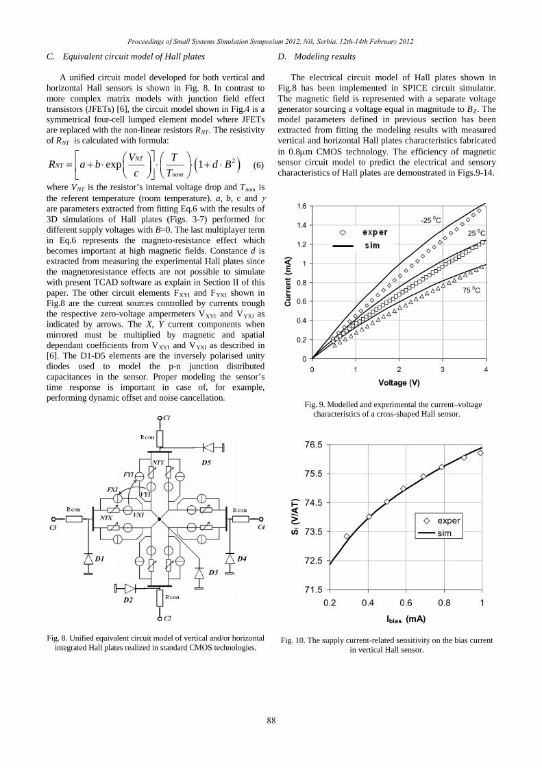
C. Equivalent circuit model of Hall plates
A unified circuit model developed for both vertical and horizontal Hall sensors is shown in Fig. 8. In contrast to more complex matrix models with junction field effect transistors (JFETs) [6], the circuit model shown in Fig.4 is a symmetrical four-cell lumped element model where JFETs are replaced with the non-linear resistors RNT. The resistivity of RNT is calculated with formula:
( )2exp 1NTNT
nom
V TR a b d Bc T
= + ⋅ ⋅ ⋅ + ⋅ (6)
where VNT is the resistor’s internal voltage drop and Tnom is the referent temperature (room temperature). a, b, c and γ are parameters extracted from fitting Eq.6 with the results of 3D simulations of Hall plates (Figs. 3-7) performed for different supply voltages with B=0. The last multiplayer term in Eq.6 represents the magneto-resistance effect which becomes important at high magnetic fields. Constance d is extracted from measuring the experimental Hall plates since the magnetoresistance effects are not possible to simulate with present TCAD software as explain in Section II of this paper. The other circuit elements FXYI and FYXI shown in Fig.8 are the current sources controlled by currents trough the respective zero-voltage ampermeters VXYI and VYXI as indicated by arrows. The X, Y current components when mirrored must be multiplied by magnetic and spatial dependant coefficients from VXYI and VYXI as described in [6]. The D1-D5 elements are the inversely polarised unity diodes used to model the p-n junction distributed capacitances in the sensor. Proper modeling the sensor’s time response is important in case of, for example, performing dynamic offset and noise cancellation.
Fig. 8. Unified equivalent circuit model of vertical and/or horizontal
integrated Hall plates realized in standard CMOS technologies.
D. Modeling results
The electrical circuit model of Hall plates shown in Fig.8 has been implemented in SPICE circuit simulator. The magnetic field is represented with a separate voltage generator sourcing a voltage equal in magnitude to BZ. The model parameters defined in previous section has been extracted from fitting the modeling results with measured vertical and horizontal Hall plates characteristics fabricated in 0.8µm CMOS technology. The efficiency of magnetic sensor circuit model to predict the electrical and sensory characteristics of Hall plates are demonstrated in Figs.9-14.
Fig. 9. Modelled and experimental the current–voltage characteristics of a cross-shaped Hall sensor.
Fig. 10. The supply current-related sensitivity on the bias current in vertical Hall sensor.
88
Proceedings of Small Systems Simulation Symposium 2012, Niš, Serbia, 12th-14th February 2012

Fig. 11. Modeling and measurements of the magnetoresistivity effects.
Fig. 12. The reduction of Hall voltage at high frequencies, due to
the presence of the distributed diode capacitance in a cross-shaped Hall sensor.
Fig. 13. Modelled and experimental a current-related magnetic
response of cross-shaped Hall sensor.
Fig. 14. Modelled and experimental Hall voltage response in
vertical Hall sensor to the magnetic field.
IV. TCAD OF MAGFETS
The inversion layer of MOSFET can be used as the active region of a magnetic sensor. This active region can exploit the Hall effect for Hall based sensors, or the carrier deflection, if the device has a split-drain. The structure of conventional Split-Drain MOSFET (MAGFET) is identical to a MOSFET but the drain is split in two or more parts as shown in Fig.15. The ability of integrating the bias and control circuitry on the same chip with MAGFET device makes this sensor structure particularly attractive.
A. TCAD study of MAGFET in CMOS technology
A MAGFET with L=125µm, W=100µm, tox=60nm
gate oxide, and substrate doping ND=1015cm-3, is studied in our case. A concave MAGFET mask layout and standard 0.35µm CMOS technology are adopted for process simulation, yielding 45µm wide drain regions separated by a 10µm oxide gap. The internal potentials and carrier distributions of the MAGFET in presence of the perpendicular magnetic field BZ were then obtained using the 3D device simulator ISE DESSIS. Fig. 16 shows the electric field distribution in the channel simulated for VGS =5V, VDS =1V and BZ =100mT, where BZ was orientated in the z-axis direction. It can be seen that the electric field iso-lines are asymmetrical with respect to the (z,x)-plane at
0=y . This asymmetry is caused by the accumulation of electrons in the upper channel region due to the influence of Lorentz force. It also causes the difference in drain currents at D1 and D2 contacts. The later is illustrated by Fig. 17 showing the drain current density distribution in the channel of MAGFET simulated without and with magnetic field BZ [12].
89
Proceedings of Small Systems Simulation Symposium 2012, Niš, Serbia, 12th-14th February 2012

Fig. 15. The 3D structure of MAGFET with carrier deflection shown in the inset.
Fig. 16 Electric field distribution in the channel of MAGFET obtained with 3D simulations for BZ=100mT.
B. Equivalent circuit model of MAGFETs
The MAGFET operation is emulated with two identical NMOSTs operating in parallel. The channel carrier transport has to be represented with two identical RC chains as illustrated in Fig. 3. Depending on the sign (+ or -) of the applied perpendicular magnetic field BZ, the equivalent resistors Rk in one of channel chains will simultaneously decrease or increase under the action of the Lorentz force due to carrier accumulation or depletion, respectively. In the expressions underlying the distributed MOSFET model [14], the magnitude of Rk is inversely proportional to the square root of the substrate doping
concentration e.g. beffN (see Eq. (A4) in Ref [13]).
Hence, in order to include magnetic effects into the existing MOSFET model, the new effective substrate doping variable beffN ′ is defined instead of the beffN parameter as:
( ),beff beff Z beff ZN N n x B N a B′ = ± ∆ = ± ⋅ (7)
where + and − signs stand for the different directions of carrier deflection in one of the NMOST channels as illustrated in Fig. 18. The Eq. (7) is the key modification to the MOSFET model [14]. It is obtained from TCAD study of MAGFET showing that there is approximately linear relation between BZ and accumulated Hall charge at the one side of the channel. The empirical constant a appearing in (4) becomes fitting parameter used to calibrate the MAGFET model. When BZ=0, the MAGFET model reverts to the original MOSFET model [14].
a)
b)
Fig. 17. Drain current density distributions near D1 and D2
MAGFET’s contacts simulated without (a) and with magnetic field Bz=40mT (b) [12].
90
Proceedings of Small Systems Simulation Symposium 2012, Niš, Serbia, 12th-14th February 2012

Fig. 18. Split-drain MAGFET represented with the two magnetic
sensitive NMOSTs
C. Modeling results
The MAGFET model is implemented in SPICE in the form of a sub-circuit with two NMOSTs as illustrated in Fig.18. As in the case of Hall plates simulation with SPICE, the magnetic field is also represented here with a separate voltage generator sourcing a voltage equal in magnitude to BZ. This voltage source drives a special “magnetic” node in the MAGFET sub-circuit that connects
BZ with the 'beffN variable of the modified MOSFET
model following Eq. (7). Fig.19 shows the comparisons between 3D simulations
and modeling results with experimental data taken from [13] of drain current imbalance 21 DDD IIi −=∆ , while the relative sensitivities of MAGFET versus VDS and VGS, for BZ=0.1T are shown on Figs. 20 and 21.
Fig. 19 The simulated, modeled and experimental MAGFET
current imbalance ∆iD dependence versus the magnetic field BZ.
Fig. 20. Relative sensitivity S of MAGFET versus: VGS extracted
from 3D device numerical simulations and from the SPICE MAGFET model.
Fig. 21. Relative sensitivity S of MAGFET versus VDS extracted
from 3D device numerical simulations and from the SPICE MAGFET model.
V. CONCLUSION In this work, the results of 3D TCAD of integrated
Hall sensor devices manufactured by using the standard AMS 0.8µm and 0.35µm high-voltage CMOS technologies are presented. The complete technology process flow and electrical characteristics of cross-shaped Hall sensor, vertical Hall sensor and MAGFET are simulated by using Silvaco (ATHENA, ATLAS) and ISE (DIOS, DESSIS, MESH, DIP) TCAD software package tools. In addition, based on the 3D numerical simulation of magnetic sensors, the efficient electrical models of these devices are derived and successfully implemented in circuit simulator SPICE.
91
Proceedings of Small Systems Simulation Symposium 2012, Niš, Serbia, 12th-14th February 2012

ACKNOWLEDGEMENT This work has been partially funded by the
Serbian Ministry for Education and Science under the projects TR-32057.
REFERENCES [1] Baltes, H.P., Popovic, R.S., "Integrated Semiconductor
Magnetic Field Sensor", Proceedings of the IEEE, Vol. 74, No. 8, August, 1986, pp. 1107-1132.
[2] Allegretto, W, Nathan, A., Baltes, H, "Numerical Analysis of Magnetic Field Sensitive Bipolar Devices", IEEE Trans. Computer-Aided Design, Vol. 10, No. 4, Feb., 1991, pp. 501-511.
[3] ATHENA User’s Manual – Process Simulation Software, SILVACO, Santa Clara, USA, 2009.
[4] ATLAS User’s Manual – Device Simulation Software, SILVACO, Santa Clara, USA, 2009.
[5] ISE TCAD – User Manual, Rel. 7.0, Integrated System Engineering AG, Zurich, Switzerland.
[6] Wachutka, G., "Unified Framework for Thermal Electrical, Magnetic and Optical SemiconductorDevice Modeling", COMPEL, Vol. 10, No. 4, 1991, pp. 311-321.
[7] Jovanovic, E., Pesic, T., Pantic, D., "3D Simulation of Cross- Shaped Hall Sensor and its Equivalent Circuit Model", Proc. of 24th International Conference on Microelectronics (MIEL’04), Vol. 1, Nis, Serbia, May 2004, pp. 235-238.
[8] Popović, R.S., Hall Effect Devices, Second edition, IOP Publishing Ltd, Bristol and Philadelphia, 2004.
[9] Popović, R.S., "The Vertical Hall-effect Device", IEEE Electron Dev. Lett., EDL-5, No. 9, 1984, pp. 357-358.
[10]Schuring, E., Demierre, M., Schott, C., Popović, R.S., "A Vertical Hall Device in CMOS High-voltage Technology", Sensors and Actuators A: Physical, Vol. 97-98, No. 1, April 2002, pp. 47-53.
[11]Jovanovic, E., Pantic, D., Pantic, D., " Simulation of Vertical Hall Sensor in High-voltage CMOS Technology ", Proc. 6th International Conference on Telecomunication in Modern Satelite, Cable and Broadcasting Services (TELSIKS’03), Vol. 2, Nis, Serbia, October 2003, pp. 811-814.
[12]Rodrigez-Torres, R., Gutierrez-D., E.A, Klima, R., Selberherr, S., "Three-Dimensional Simulation Split-Drain MAGFET at 300K and 77K", Proc. 32rd European Solid-State Research Conference (ESSDERC 2002), September 2003, pp. 151-154.
[13]Torres, R., Klima, R., Selberherr, S., "Analysis of Split-Drain MAGFETs", IEEE Electron Devices, Vol. 51, No. 12, 2004, pp. 2237-2245.
[14]Pesic, T., Jankovic, N., "A Compact Non-Quasi_Static MOSFET Model Based on the Equivalent Non-linear Transmission Line", IEEE Trans. On Computer-Aided Design of Integrated Circuits and Systems, Vol. 24, No. 10, October 2005, pp. 1550-1561.
92
Proceedings of Small Systems Simulation Symposium 2012, Niš, Serbia, 12th-14th February 2012