Embed Size (px)
Citation preview
Fly and Shoot Game Using FPGA-based ApproachWing Cheong Tam
Computer Science DepartmentSan Jose State University
San Jose, CA 95192408-924-1000
ABSTRACTFPGA (Field Programmable Gate Array) is an integrated circuit that can be reprogrammed to debug and refine the design after manufacturing [1]. Due to the ease of implementation and configuration, FPGA is an ideal solution to many high speed computer architectures that require extensive testing and prototyping. In this sense, a Fly and Shoot Game is developed by using the FPGA-based approach, where player can fly the fighter aircraft and shoot the opponents. The physics phenomena, such as acceleration, inertia and collisions have been implemented to enhance the user experience. The program is implemented with all the desired features and is tested thoroughly on Cyclone II EP2C20F484C7N FPGA board using Verilog hardware description language. This paper describes the design of the architecture, the implementation schemes, the difficulties encountered and the optimization of algorithm for hardware mapping.
1. INTRODUCTIONThis application is a FPGA-based single-player plane shooting game, where player can gain control over the fighter aircraft. Player can fly to the left, right, accelerate and shoot. A yellow flying object represents the player’s aircraft whereas the other blue flying objects represent the enemies. Throughout the game, enemies are randomly generated through the program. Player has to destroy the enemies to stay alive. On the contrary, the game is over if the player crashes into the enemies. This report covers the hardware, Verilog implementation and the difficulties encountered during the project. Chapter 2 talks about the Game Logic Module, such as event handling and control logic of the Push Button Switches. Chapter 3 describes the implementation of the VGA Controller and Chapter 4 explains the LFSR-based pseudo-random number generator.
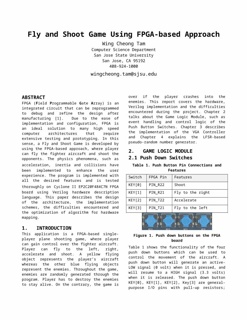
2. GAME LOGIC MODULE2.1 Push Down Switches
Table 1. Push Button Pin Connections and Features
Switch FPGA Pin Features
KEY[0] PIN_R22 Shoot
KEY[1] PIN_R21 Fly to the right
KEY[2] PIN_T22 Accelerate
KEY[3] PIN_T21 Fly to the left
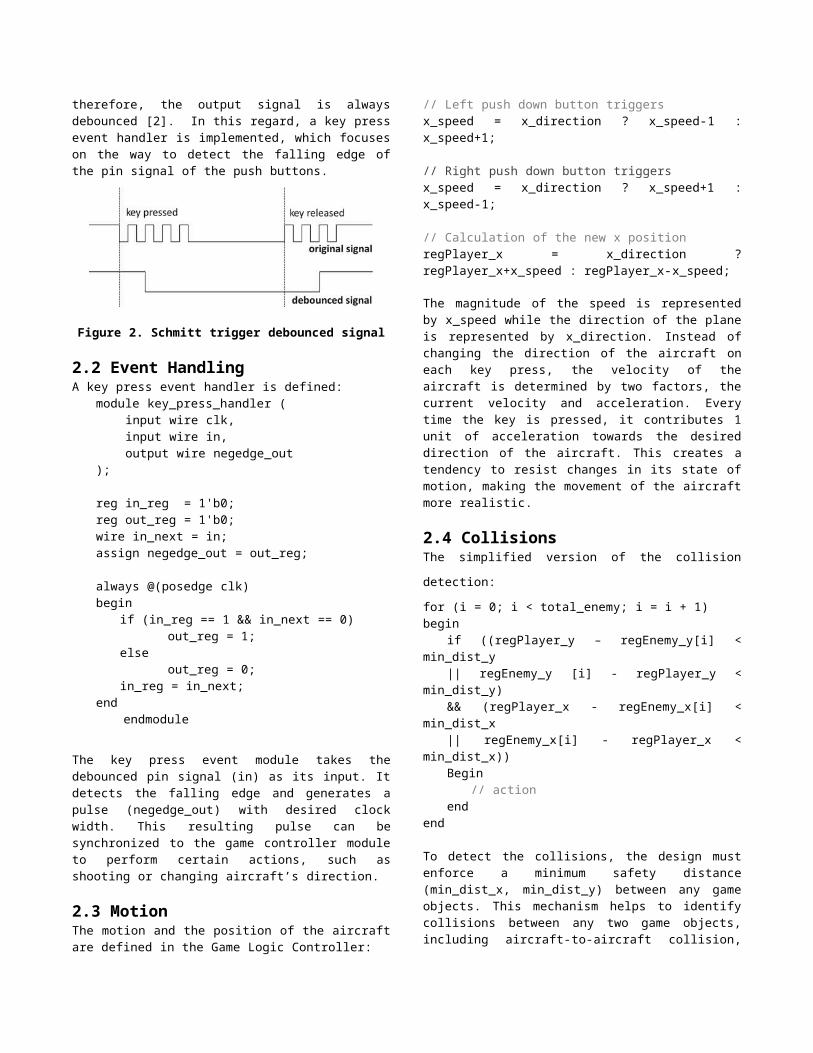
Figure 1. Push down buttons on the FPGA boardTable 1 shows the functionality of the four push down buttons which can be used to control the movement of the aircraft. A push down button will generate an active-LOW signal (0 volt) when it is pressed, and will resume to a HIGH signal (3.3 volts) when it is released. The push down button KEY[0], KEY[1], KEY[2], Key[3] are general-purpose I/O pins with pull-up resistors; therefore, the output signal is always debounced [2]. In this regard, a key press event handler is implemented, which focuses on the way to detect the falling edge of the pin signal of the push buttons.
Figure 2. Schmitt trigger debounced signal
2.2 Event HandlingA key press event handler is defined:
module key_press_handler ( input wire clk, input wire in, output wire negedge_out);
reg in_reg = 1'b0;reg out_reg = 1'b0;wire in_next = in;assign negedge_out = out_reg;
always @(posedge clk)begin
if (in_reg == 1 && in_next == 0)out_reg = 1;
elseout_reg = 0;
in_reg = in_next;end
endmodule
The key press event module takes the debounced pin signal (in) as its input. It detects the falling edge and generates a pulse (negedge_out) with desired clock width. This resulting pulse can be synchronized to the game controller module to perform certain actions, such as shooting or changing aircraft’s direction.
2.3 MotionThe motion and the position of the aircraft are defined in the Game Logic Controller:// Left push down button triggersx_speed = x_direction ? x_speed-1 : x_speed+1;
// Right push down button triggersx_speed = x_direction ? x_speed+1 : x_speed-1;
// Calculation of the new x positionregPlayer_x = x_direction ? regPlayer_x+x_speed : regPlayer_x-x_speed;
The magnitude of the speed is represented by x_speed while the direction of the plane is represented by x_direction. Instead of changing the direction of the aircraft on each key press, the velocity of the aircraft is determined by two factors, the current velocity and acceleration. Every time the key is pressed, it contributes 1 unit of acceleration towards the desired direction of the aircraft. This creates a tendency to resist changes in its state of motion, making the movement of the aircraft more realistic.
2.4 CollisionsThe simplified version of the collision detection:
for (i = 0; i < total_enemy; i = i + 1)begin
if ((regPlayer_y – regEnemy_y[i] < min_dist_y
|| regEnemy_y [i] - regPlayer_y < min_dist_y)
&& (regPlayer_x - regEnemy_x[i] < min_dist_x
|| regEnemy_x[i] - regPlayer_x < min_dist_x))
Begin// action
endend
To detect the collisions, the design must enforce a minimum safety distance (min_dist_x, min_dist_y) between any game objects. This mechanism helps to identify collisions between any two game objects, including aircraft-to-aircraft collision, bullet-to-aircraft collision and aircraft-to-border detection.
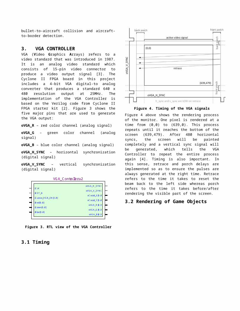
3. VGA CONTROLLERVGA (Video Graphics Arrays) refers to a video standard that was introduced in 1987. It is an analog video standard which consists of 15-pin video connector to produce a video output signal [3]. The Cyclone II FPGA board in this project includes a 4-bit VGA digital-to analog converter that produces a standard 640 x 480 resolution output at 25MHz. The implementation of the VGA Controller is based on the Verilog code from Cyclone II FPGA starter kit [2]. Figure 3 shows the five major pins that are used to generate the VGA output:
oVGA_R – red color channel (analog signal)
oVGA_G – green color channel (analog signal)
oVGA_B – blue color channel (analog signal)
oVGA_H_SYNC – horizontal synchronization (digital signal)
oVGA_V_SYNC – vertical synchronization (digital signal)
SELDATAA
DATABOUT0
MUX21
SELDATAA
DATABOUT0
MUX21
IN[2..0] OUT[7..0]
DECODER
SEL
DATAA
DATAB
OUT0
MUX21
SEL
DATAA
DATAB
OUT0
MUX21
+A[11..0]
B[11..0]
ADDER
SELDATAA
DATABOUT0
MUX21
<A[31..0]
B[31..0]
LESS_THAN
+A[11..0]
B[11..0]
ADDER
SELDATAA
DATABOUT0
MUX21
SELDATAA
DATABOUT0
MUX21
<A[31..0]
B[31..0]
LESS_THAN
+A[11..0]
B[11..0]
ADDER
SELDATAA
DATABOUT0
MUX21
<A[31..0]
B[31..0]
LESS_THAN
+A[11..0]
B[11..0]
ADDER
SELDATAA
DATABOUT0
MUX21
<A[31..0]
B[31..0]
LESS_THAN
inclk0 c0
iPlayer_F
iVGA_CLK
iVGA_X[9..0]
iVGA_Y[9..0]
iPlayer_X[9..0]
iPlayer_Y[9..0]
iEnemy_X[79..0]
iEnemy_Y[79..0]
iBullet_X[39..0]
iBullet_Y[39..0]
oRed[9..0]
oGreen[9..0]
oBlue[9..0]
iCLK
iRST_N
iCursor_RGB_EN[3..0]
iRed[9..0]
iGreen[9..0]
iBlue[9..0]
oVGA_H_SYNC
oVGA_V_SYNC
oCoord_X[9..0]
oCoord_Y[9..0]
oVGA_R[0..9]
oVGA_G[0..9]
oVGA_B[0..9]
+A[32..0]
B[32..0]
ADDER
+A[5..0]
B[5..0]
ADDER
SELDATAA
DATABOUT0
MUX21
+A[4..0]
B[4..0]
ADDER
0
10
+A[5..0]
B[5..0]
ADDER
SELDATAA
DATABOUT0
MUX21
+A[4..0]
B[4..0]
ADDER
0
10
+A[4..0]
B[4..0]
ADDER
SELDATAA
DATABOUT0
MUX21
+A[5..0]
B[5..0]
ADDER
0
11
+A[9..0]
B[9..0]
ADDER
SELDATAA
DATABOUT0
MUX21
SELDATAA
DATABOUT0
MUX21
+A[10..0]
B[10..0]
ADDER
<A[9..0]
B[9..0]
LESS_THAN
SELDATAA
DATABOUT0
MUX21
0
10
1
<A[9..0]
B[9..0]
LESS_THAN
SELDATAA
DATABOUT0
MUX21
+A[11..0]
B[11..0]
ADDER
+A[11..0]
B[11..0]
ADDER
+A[11..0]
B[11..0]
ADDER
+A[11..0]
B[11..0]
ADDER
+A[11..0]
B[11..0]
ADDER
regENEMY_Y~_OUT0
regENEMY_Y~_OUT0
regENEMY_Y~_OUT0
regENEMY_Y~_OUT0regENEMY_Y~_OUT0regENEMY_Y~_OUT0
regENEMY_Y~_OUT0regENEMY_Y~_OUT0
regENEMY_Y~_OUT0regENEMY_HEAD_OUT0
Decoder0_OUT
current_enemy_gen_state_OUT0
always1~50_OUT0
regENEMY_Y~_OUT0
regENEMY_Y~_OUT0regENEMY_Y~_OUT0regENEMY_Y~_OUT0
regENEMY_Y~_OUT0
always1~36_OUT0
regENEMY_Y~_OUT0
regENEMY_Y~_OUT0regENEMY_Y~_OUT0
always1~33_OUT0
regBullet_Y~_OUT0
regENEMY_Y~_OUT0
always1~27_OUT0
LessThan49_OUT
regENEMY_Y~_OUT0always1~29_OUT0
LessThan52_OUT
regENEMY_Y~_OUT0always1~32_OUT0
regBullet_Y~_OUT0
LessThan55_OUT
always1~30_OUT0
regBullet_Y~_OUT0
LessThan58_OUT
regPlayer_F[0]_OUT0
regPLAYER_X_OUT0regPLAYER_Y_OUT0
regENEMY_X[0]_OUT0regENEMY_X[1]_OUT0regENEMY_X[2]_OUT0regENEMY_X[3]_OUT0regENEMY_X[4]_OUT0regENEMY_X[5]_OUT0regENEMY_X[6]_OUT0regENEMY_X[7]_OUT0regENEMY_Y[0]_OUT0regENEMY_Y[1]_OUT0regENEMY_Y[2]_OUT0regENEMY_Y[3]_OUT0regENEMY_Y[4]_OUT0regENEMY_Y[5]_OUT0regENEMY_Y[6]_OUT0regENEMY_Y[7]_OUT0
regBullet_X[0]_OUT0
regBullet_Y[0]_OUT0
counter_OUT0
Add1_OUT
x_speed_OUT0x_speed~_OUT0
x_direction_OUT0
Equal0_OUT
x_direction~0_OUT0
y_speed_OUT0y_speed~_OUT0
y_direction_OUT0
Equal1_OUT
y_direction~0_OUT0
x_speed~_OUT0
x_speed~_OUT0
x_direction~1_OUT0
Equal2_OUT
x_direction~2_OUT0
x_speed~_OUT0
LessThan1_OUT
x_speed~_OUT0
x_direction~3_OUT0
x_direction~5_OUT0
regPLAYER_X~_OUT0
Add39_OUT
Add26_OUT
Add23_OUT
Add46_OUT
Add43_OUT
regENEMY_Y~[759..750]
10' h000 --
regENEMY_Y~[839..760]
Decoder0
always1~50
regENEMY_Y~[309..270]
regENEMY_Y~[259..230]
Add531' h0 --
1' h1 --
1' h0 --
1' h1 --
regBullet_Y~[19..10]
10' h000 --
LessThan49
32' h00000028 --
regBullet_Y~[29..20]
10' h000 --
regBullet_Y~[39..30]
LessThan52
32' h00000028 --
Add611' h0 --
1' h1 --
1' h0 --
1' h1 --
regBullet_Y~[49..40]
10' h000 --
LessThan55
32' h00000028 --
Add651' h0 --
1' h1 --
1' h0 --
1' h1 --
regBullet_Y~[59..50]
LessThan58
32' h00000028 --
VGA_Audio_PLL:u1
CLOCK_27[1..0]
VGA_HS
VGA_VSVGA_R[3..0]VGA_G[3..0]VGA_B[3..0]
Add1
33' h000000001 --
Add2
1' h1 --
6' h3D --
x_speed~[4..0]Add3
5' h01 --
x_direction~0
Add4
1' h1 --
6' h3D --
y_speed~[4..0]Add5
5' h01 --
y_direction~0
Add6
5' h01 --
x_speed~[14..10]Add7
1' h1 --
6' h3D --
x_direction~2
Add8
5' h00 --
x_speed~[24..20]
5' h04 --
regPLAYER_X~[9..0]Add9
1' h1 --
5' h1F --
1' h1 --
LessThan3
10' h014 --
regPLAYER_X~[19..10]
10' h014 --
x_direction~4x_direction~5
LessThan4
10' h26C --
regPLAYER_X~[29..20]
10' h26C --
Add391' h0 --
1' h1 --
1' h0 --
1' h1 --
Add261' h0 --
1' h1 --
1' h0 --
1' h1 --
Add231' h0 --
1' h1 --
1' h0 --
1' h1 --
Add461' h0 --
1' h1 --
1' h0 --
1' h1 --
Add431' h0 --
1' h1 --
1' h0 --
1' h1 --
Add571' h0 --
1' h1 --
1' h0 --
1' h1 --
VGA_Pattern:u3
30' h00000000 --
30' h00000000 --
VGA_Controller:u2
4' h7 --
Figure 3. RTL view of the VGA Controller
3.1 Timing
Figure 4. Timing of the VGA signalsFigure 4 above shows the rendering process of the monitor. One pixel is rendered at a time from (0,0) to (639,0). This process repeats until it reaches the bottom of the screen (639,479). After 480 horizontal syncs, the screen will be painted completely and a vertical sync signal will be generated, which tells the VGA
Controller to repeat the entire process again [4]. Timing is also important. In this sense, retrace and porch delays are implemented so as to ensure the pulses are always generated at the right time. Retrace refers to the time it takes to reset the beam back to the left side whereas porch refers to the time it takes before/after rendering the visible part of the screen.
3.2 Rendering of Game ObjectsEvery visible game object is made up of rectangles. For this reason, a rectangle renderer is implemented as the fundamental part of different rendering modules:isRect = ((iOBJ_X - iVGA_X <= iOBJ_W/2 || iVGA_X - iOBJ_X <= iOBJ_W/2) && (iOBJ_Y - iVGA_Y <= iOBJ_H/2 || iVGA_Y - iOBJ_Y <= iOBJ_H/2));
Figure 5. Overview of the Game ModulesFigure 5 shows the overview of the structural implementation of this game. The Game Logic Module, which is the most consuming part of the game, is responsible for all the in-game interactions and dynamics. When there is an update in the Game Logic Module, Game Object Renderer updates accordingly. The state of the Game Object Renderer is determined by two inputs: the coordinate of the pixel and the control signal. As the VGA Controller scans across the screen, the control signal or the screen coordinates change. Therefore, while the VGA Controller is filling up the screen, a 1-pixel RGB signal will be re-computed at a time. This process repeats for every horizontal line. Consequently, all game objects will be displayed on the screen once the electron beam reaches the bottom part of the screen.
4. RANDOM NUMBER GENERATORDuring the gameplay, enemies are randomly generated through the program. In order to randomize the enemy’s attacks, a random number generator is needed. A good random number must be unpredictable and evenly distributed. In fact, generating a perfect random number is a hard mathematical problem, so it could not be synthesized using the standard Verilog. As the
result, a LFSR-based random number generator was implemented for this purpose.
Figure 6. 7-bit linear feedback shift register (LFSR)
4.1 Linear Feedback Shift RegisterLFSR (Linear Feedback Shift Register) is a register that the input bit is a linear function of its previous state. A well-chosen feedback function can produce a sequence of bits that appears randomly and has a long cycle [5]. This architecture is fast as it uses only XOR gate and a seed to compute new random numbers (Figure 6). However, the tradeoff of this optimization is the quality of the random number, because LFSR generates pseudo-random numbers, rather than true random numbers.
The polynomial equation, which defines as below, produces a 7-bit maximum-cycle LFSR.
(1)Based on the linear feedback function (1), the random number is defined below using Verilog HDL:r = seed_value;r = { r[5:0], r[6] ^ r[5] };
The 7-bit LFSR produces pseudo-random numbers with 2n-1
cycles, which randomizes 127 different positions to generate the enemies along the x-axis. A standard VGA monitor uses 640x480 pixels in resolution. To spawn the enemies across the center part of the screen evenly, two procedures were taken. The first step is to left shift the random number by two bits in order to increase the gap between each enemy. The second step is to implement a porch so as to avoid generating the enemy objects at the edge of the screen.
5. CONCLUSIONThis paper presents the Verilog implementation of a simple Fly and Shoot game using the FPGA approach. Three major components, including Game Logic Module, VGA Controller and Random Number Generator were discussed. The application is completed successfully and tested thoroughly. The final product is shown as Figure 7.
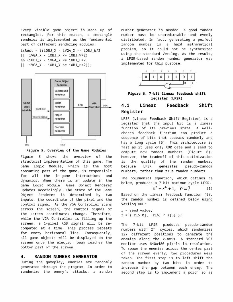
Figure 7. Screenshot of the Fly and Shoot Game
6. REFERENCES[1] V. Hopkin and B. Kirk, "FPGA Migration to ASICs,"
WESCON Conf. Record Microel. Comm. Techn., 1995.
[2] Cyclone II FPGA Starter Development Board: Reference Manual, 1st ed. Altera Corporation, 2006.
[3] W. Aihua, D. Liu, and Z. Wang, "The design Of VGA data communication based on FPGA." IT in Medicine and Education (ITME), 2011 International Symposium on. Vol. 1. IEEE, 2011.
[4] H. Dong and G. Hongmin. "Design of VGA display controller based on FPGA and VHDL." Electric Information and Control Engineering (ICEICE), 2011 International Conference on. IEEE, 2011.
[5] S.S. Krivenko and S.A. Krivenko, "Many-to-many linear-feedback shift register." Electronics and Nanotechnology (ELNANO), 2014 IEEE 34th International Conference on. IEEE, 2014.