Embed Size (px)
Citation preview
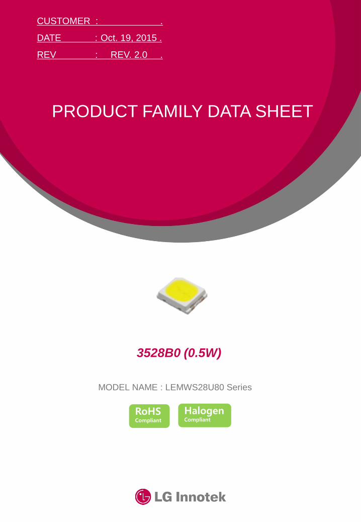
PRODUCT FAMILY DATA SHEET
3528B0 (0.5W)
CUSTOMER : .
DATE : Oct. 19, 2015 .
REV : REV. 2.0 .
MODEL NAME : LEMWS28U80 Series Halogen Compliant
RoHS Compliant
2 / 29
CONTENTS
1. Features -------------------------------------------------------------
2. Applications --------------------------------------------------------
3. Outline Dimensions ----------------------------------------------
4. Absolute Maximum Ratings -----------------------------------
5. Electro-Optical Characteristics --------------------------------
6. Flux Characteristics and Order Code ------------------------
7. Chromaticity Bins -------------------------------------------------
8. Typical Characteristic Curves ---------------------------------
9. Reliability Test Items and Conditions ------------------------
10. Packing and Labeling of Products --------------------------
11. Cautions on Use -------------------------------------------------
Appendix ---------------------------------------------------------------
3
3
3
4
4 ~ 5
6
7 ~ 10
11 ~ 19
20
21 ~ 23
24 ~ 27
28
3 / 29
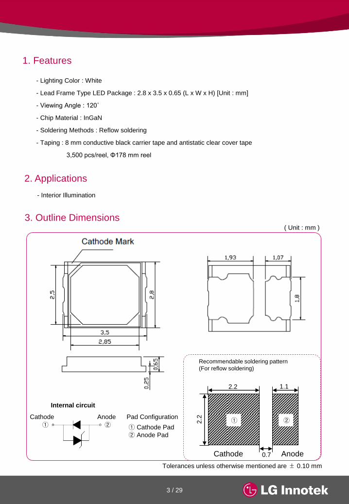
3. Outline Dimensions
2. Applications
( Unit : mm )
Tolerances unless otherwise mentioned are ± 0.10 mm
Recommendable soldering pattern
(For reflow soldering)
① Cathode Pad
② Anode Pad
Pad Configuration
Internal circuit
1.1
②
Anode Cathode 0.7
2.2
2.2
① Cathode
① ②
Anode
1. Features
- Lighting Color : White
- Lead Frame Type LED Package : 2.8 x 3.5 x 0.65 (L x W x H) [Unit : mm]
- Viewing Angle : 120˚
- Chip Material : InGaN
- Soldering Methods : Reflow soldering
- Taping : 8 mm conductive black carrier tape and antistatic clear cover tape
3,500 pcs/reel, Φ178 mm reel
- Interior Illumination
4 / 29
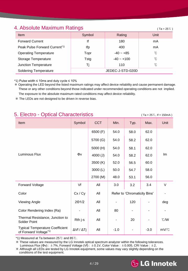
( Ta = 25℃ )
Item Symbol Rating Unit
Forward Current If 180 mA
Peak Pulse Forward Current*1) Ifp 400 mA
Operating Temperature Topr -40 ~ +85 ℃
Storage Temperature Tstg -40 ~ +100 ℃
Junction Temperature Tj 110 ℃
Soldering Temperature JEDEC-J-STD-020D
( Ta = 25℃, If = 150mA )
Item Symbol CCT Min. Typ. Max. Unit
Luminous Flux Φv
6500 (F) 54.0 58.0 62.0
lm
5700 (G) 54.0 58.2 62.0
5000 (H) 54.0 58.1 62.0
4000 (J) 54.0 58.2 62.0
3500 (K) 52.0 56.5 60.0
3000 (L) 50.0 54.7 58.0
2700 (M) 48.0 53.1 56.0
Forward Voltage Vf All 3.0 3.2 3.4 V
Color Cx / Cy All Refer to ‘Chromaticity Bins' -
Viewing Angle 2Θ1/2 All - 120 - deg
Color Rendering Index (Ra) - All 80 - - -
Thermal Resistance, Junction to
Solder Point Rth j-s All - 20 - ℃/W
Typical Temperature Coefficient
of Forward Voltage*1) ΔVf / ΔTj All -1.0 - -3.0 mV/℃
4. Absolute Maximum Ratings
5. Electro - Optical Characteristics
*1) Pulse width ≤ 10ms and duty cycle ≤ 10%
※ Operating the LED beyond the listed maximum ratings may affect device reliability and cause permanent damage.
These or any other conditions beyond those indicated under recommended operating conditions are not implied.
The exposure to the absolute maximum rated conditions may affect device reliability.
※ The LEDs are not designed to be driven in reverse bias.
*1) Measured at Ta between 25℃ and 85℃.
※ These values are measured by the LG Innotek optical spectrum analyzer within the following tolerances. Luminous Flux (Φv) : ±7%, Forward Voltage (Vf) : ±0.1V, Color Value : ±0.005, CRI Value : ±2, ※ Although all LEDs are tested by LG Innotek equipment, some values may vary slightly depending on the conditions of the test equipment.
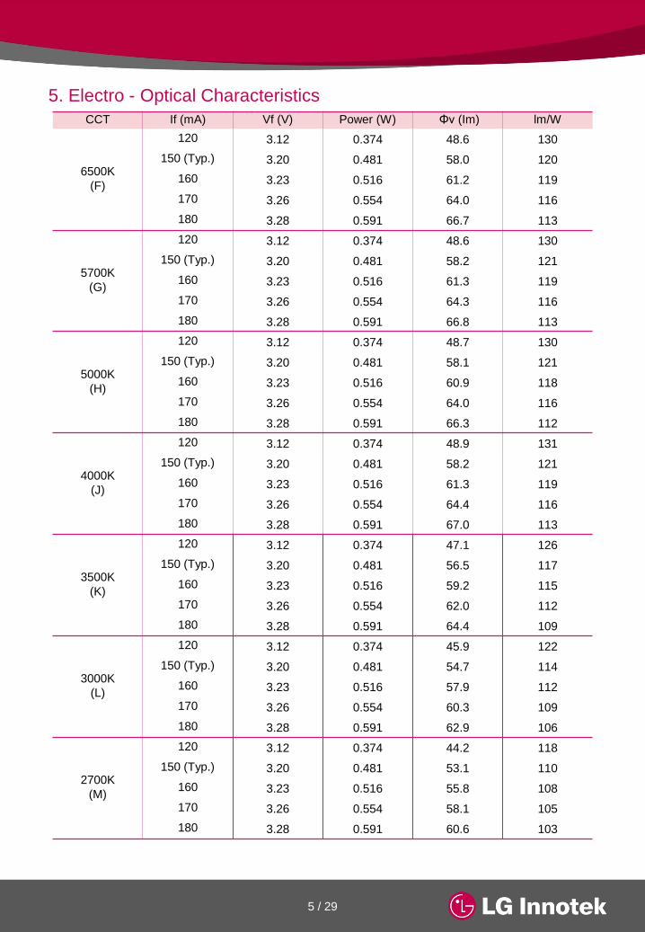
5 / 29
CCT If (mA) Vf (V) Power (W) Φv (Im) lm/W
6500K
(F)
120 3.12 0.374 48.6 130
150 (Typ.) 3.20 0.481 58.0 120
160 3.23 0.516 61.2 119
170 3.26 0.554 64.0 116
180 3.28 0.591 66.7 113
5700K
(G)
120 3.12 0.374 48.6 130
150 (Typ.) 3.20 0.481 58.2 121
160 3.23 0.516 61.3 119
170 3.26 0.554 64.3 116
180 3.28 0.591 66.8 113
5000K
(H)
120 3.12 0.374 48.7 130
150 (Typ.) 3.20 0.481 58.1 121
160 3.23 0.516 60.9 118
170 3.26 0.554 64.0 116
180 3.28 0.591 66.3 112
4000K
(J)
120 3.12 0.374 48.9 131
150 (Typ.) 3.20 0.481 58.2 121
160 3.23 0.516 61.3 119
170 3.26 0.554 64.4 116
180 3.28 0.591 67.0 113
3500K
(K)
120 3.12 0.374 47.1 126
150 (Typ.) 3.20 0.481 56.5 117
160 3.23 0.516 59.2 115
170 3.26 0.554 62.0 112
180 3.28 0.591 64.4 109
3000K
(L)
120 3.12 0.374 45.9 122
150 (Typ.) 3.20 0.481 54.7 114
160 3.23 0.516 57.9 112
170 3.26 0.554 60.3 109
180 3.28 0.591 62.9 106
2700K
(M)
120 3.12 0.374 44.2 118
150 (Typ.) 3.20 0.481 53.1 110
160 3.23 0.516 55.8 108
170 3.26 0.554 58.1 105
180 3.28 0.591 60.6 103
5. Electro - Optical Characteristics

6 / 29
Color CRI CCT Vf @ 60mA
[V]
Luminous Flux [lm]
@ 60mA Order Code
Bin Code
Min. Max.
Cool 80 6500
(F)
3.00 ~ 3.10 (1)
3.10 ~ 3.20 (2)
3.20 ~ 3.30 (3)
3.30 ~ 3.40 (4)
U 54.0 62.0 LEMWS28U80FSZ2xx
Cool 80 5700
(G)
3.00 ~ 3.10 (1)
3.10 ~ 3.20 (2)
3.20 ~ 3.30 (3)
3.30 ~ 3.40 (4)
U 54.0 62.0 LEMWS28U80GSZ2xx
Cool 80 5000
(H)
3.00 ~ 3.10 (1)
3.10 ~ 3.20 (2)
3.20 ~ 3.30 (3)
3.30 ~ 3.40 (4)
U 54.0 62.0 LEMWS28U80HSZ2xx
Neutral 80 4000
(J)
3.00 ~ 3.10 (1)
3.10 ~ 3.20 (2)
3.20 ~ 3.30 (3)
3.30 ~ 3.40 (4)
U 54.0 62.0 LEMWS28U80JSZ2xx
Warm 80 3500
(K)
3.00 ~ 3.10 (1)
3.10 ~ 3.20 (2)
3.20 ~ 3.30 (3)
3.30 ~ 3.40 (4)
U 52.0 60.0 LEMWS28U80KSZ2xx
Warm 80 3000
(L)
3.00 ~ 3.10 (1)
3.10 ~ 3.20 (2)
3.20 ~ 3.30 (3)
3.30 ~ 3.40 (4)
U 50.0 58.0 LEMWS28U80LSZ2xx
Warm 80 2700
(M)
3.00 ~ 3.10 (1)
3.10 ~ 3.20 (2)
3.20 ~ 3.30 (3)
3.30 ~ 3.40 (4)
U 48.0 56.0 LEMWS28U80MSZ2xx
6. Flux Characteristics and Order Code
※ Φv values are for representative references only.
7 / 29
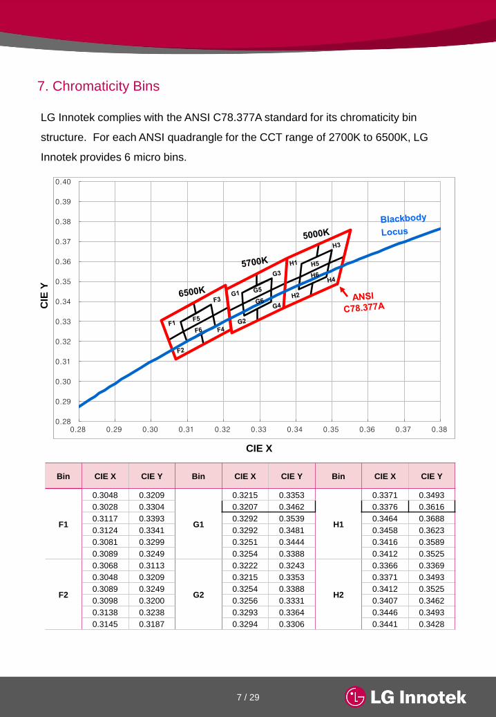
LG Innotek complies with the ANSI C78.377A standard for its chromaticity bin
structure. For each ANSI quadrangle for the CCT range of 2700K to 6500K, LG
Innotek provides 6 micro bins.
CIE
Y
CIE X
Bin CIE X CIE Y Bin CIE X CIE Y Bin CIE X CIE Y
F1
0.3048 0.3209
G1
0.3215 0.3353
H1
0.3371 0.3493
0.3028 0.3304 0.3207 0.3462 0.3376 0.3616
0.3117 0.3393 0.3292 0.3539 0.3464 0.3688
0.3124 0.3341 0.3292 0.3481 0.3458 0.3623
0.3081 0.3299 0.3251 0.3444 0.3416 0.3589
0.3089 0.3249 0.3254 0.3388 0.3412 0.3525
F2
0.3068 0.3113
G2
0.3222 0.3243
H2
0.3366 0.3369
0.3048 0.3209 0.3215 0.3353 0.3371 0.3493
0.3089 0.3249 0.3254 0.3388 0.3412 0.3525
0.3098 0.3200 0.3256 0.3331 0.3407 0.3462
0.3138 0.3238 0.3293 0.3364 0.3446 0.3493
0.3145 0.3187 0.3294 0.3306 0.3441 0.3428
7. Chromaticity Bins
0.28
0.29
0.30
0.31
0.32
0.33
0.34
0.35
0.36
0.37
0.38
0.39
0.40
0.28 0.29 0.30 0.31 0.32 0.33 0.34 0.35 0.36 0.37 0.38
8 / 29
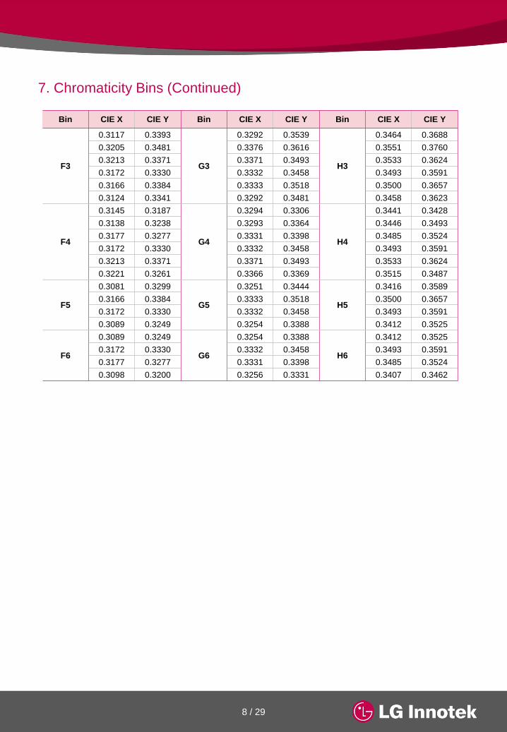
Bin CIE X CIE Y Bin CIE X CIE Y Bin CIE X CIE Y
F3
0.3117 0.3393
G3
0.3292 0.3539
H3
0.3464 0.3688
0.3205 0.3481 0.3376 0.3616 0.3551 0.3760
0.3213 0.3371 0.3371 0.3493 0.3533 0.3624
0.3172 0.3330 0.3332 0.3458 0.3493 0.3591
0.3166 0.3384 0.3333 0.3518 0.3500 0.3657
0.3124 0.3341 0.3292 0.3481 0.3458 0.3623
F4
0.3145 0.3187
G4
0.3294 0.3306
H4
0.3441 0.3428
0.3138 0.3238 0.3293 0.3364 0.3446 0.3493
0.3177 0.3277 0.3331 0.3398 0.3485 0.3524
0.3172 0.3330 0.3332 0.3458 0.3493 0.3591
0.3213 0.3371 0.3371 0.3493 0.3533 0.3624
0.3221 0.3261 0.3366 0.3369 0.3515 0.3487
F5
0.3081 0.3299
G5
0.3251 0.3444
H5
0.3416 0.3589
0.3166 0.3384 0.3333 0.3518 0.3500 0.3657
0.3172 0.3330 0.3332 0.3458 0.3493 0.3591
0.3089 0.3249 0.3254 0.3388 0.3412 0.3525
F6
0.3089 0.3249
G6
0.3254 0.3388
H6
0.3412 0.3525
0.3172 0.3330 0.3332 0.3458 0.3493 0.3591
0.3177 0.3277 0.3331 0.3398 0.3485 0.3524
0.3098 0.3200 0.3256 0.3331 0.3407 0.3462
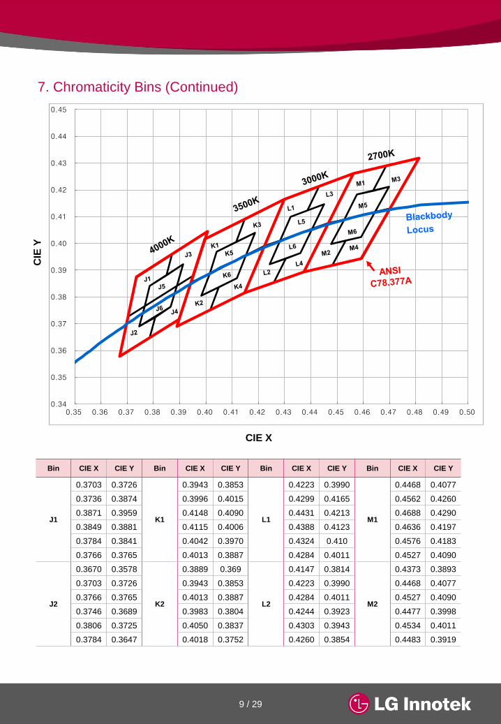
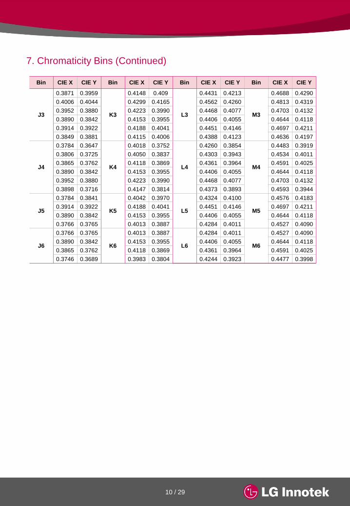
7. Chromaticity Bins (Continued)
9 / 29
CIE X
CIE
Y
Bin CIE X CIE Y Bin CIE X CIE Y Bin CIE X CIE Y Bin CIE X CIE Y
J1
0.3703 0.3726
K1
0.3943 0.3853
L1
0.4223 0.3990
M1
0.4468 0.4077
0.3736 0.3874 0.3996 0.4015 0.4299 0.4165 0.4562 0.4260
0.3871 0.3959 0.4148 0.4090 0.4431 0.4213 0.4688 0.4290
0.3849 0.3881 0.4115 0.4006 0.4388 0.4123 0.4636 0.4197
0.3784 0.3841 0.4042 0.3970 0.4324 0.410 0.4576 0.4183
0.3766 0.3765 0.4013 0.3887 0.4284 0.4011 0.4527 0.4090
J2
0.3670 0.3578
K2
0.3889 0.369
L2
0.4147 0.3814
M2
0.4373 0.3893
0.3703 0.3726 0.3943 0.3853 0.4223 0.3990 0.4468 0.4077
0.3766 0.3765 0.4013 0.3887 0.4284 0.4011 0.4527 0.4090
0.3746 0.3689 0.3983 0.3804 0.4244 0.3923 0.4477 0.3998
0.3806 0.3725 0.4050 0.3837 0.4303 0.3943 0.4534 0.4011
0.3784 0.3647 0.4018 0.3752 0.4260 0.3854 0.4483 0.3919
7. Chromaticity Bins (Continued)
0.34
0.35
0.36
0.37
0.38
0.39
0.40
0.41
0.42
0.43
0.44
0.45
0.35 0.36 0.37 0.38 0.39 0.40 0.41 0.42 0.43 0.44 0.45 0.46 0.47 0.48 0.49 0.50
10 / 29
7. Chromaticity Bins (Continued)
Bin CIE X CIE Y Bin CIE X CIE Y Bin CIE X CIE Y Bin CIE X CIE Y
J3
0.3871 0.3959
K3
0.4148 0.409
L3
0.4431 0.4213
M3
0.4688 0.4290
0.4006 0.4044 0.4299 0.4165 0.4562 0.4260 0.4813 0.4319
0.3952 0.3880 0.4223 0.3990 0.4468 0.4077 0.4703 0.4132
0.3890 0.3842 0.4153 0.3955 0.4406 0.4055 0.4644 0.4118
0.3914 0.3922 0.4188 0.4041 0.4451 0.4146 0.4697 0.4211
0.3849 0.3881 0.4115 0.4006 0.4388 0.4123 0.4636 0.4197
J4
0.3784 0.3647
K4
0.4018 0.3752
L4
0.4260 0.3854
M4
0.4483 0.3919
0.3806 0.3725 0.4050 0.3837 0.4303 0.3943 0.4534 0.4011
0.3865 0.3762 0.4118 0.3869 0.4361 0.3964 0.4591 0.4025
0.3890 0.3842 0.4153 0.3955 0.4406 0.4055 0.4644 0.4118
0.3952 0.3880 0.4223 0.3990 0.4468 0.4077 0.4703 0.4132
0.3898 0.3716 0.4147 0.3814 0.4373 0.3893 0.4593 0.3944
J5
0.3784 0.3841
K5
0.4042 0.3970
L5
0.4324 0.4100
M5
0.4576 0.4183
0.3914 0.3922 0.4188 0.4041 0.4451 0.4146 0.4697 0.4211
0.3890 0.3842 0.4153 0.3955 0.4406 0.4055 0.4644 0.4118
0.3766 0.3765 0.4013 0.3887 0.4284 0.4011 0.4527 0.4090
J6
0.3766 0.3765
K6
0.4013 0.3887
L6
0.4284 0.4011
M6
0.4527 0.4090
0.3890 0.3842 0.4153 0.3955 0.4406 0.4055 0.4644 0.4118
0.3865 0.3762 0.4118 0.3869 0.4361 0.3964 0.4591 0.4025
0.3746 0.3689 0.3983 0.3804 0.4244 0.3923 0.4477 0.3998
11 / 29
Fo
rward
Curr
ent [m
A]
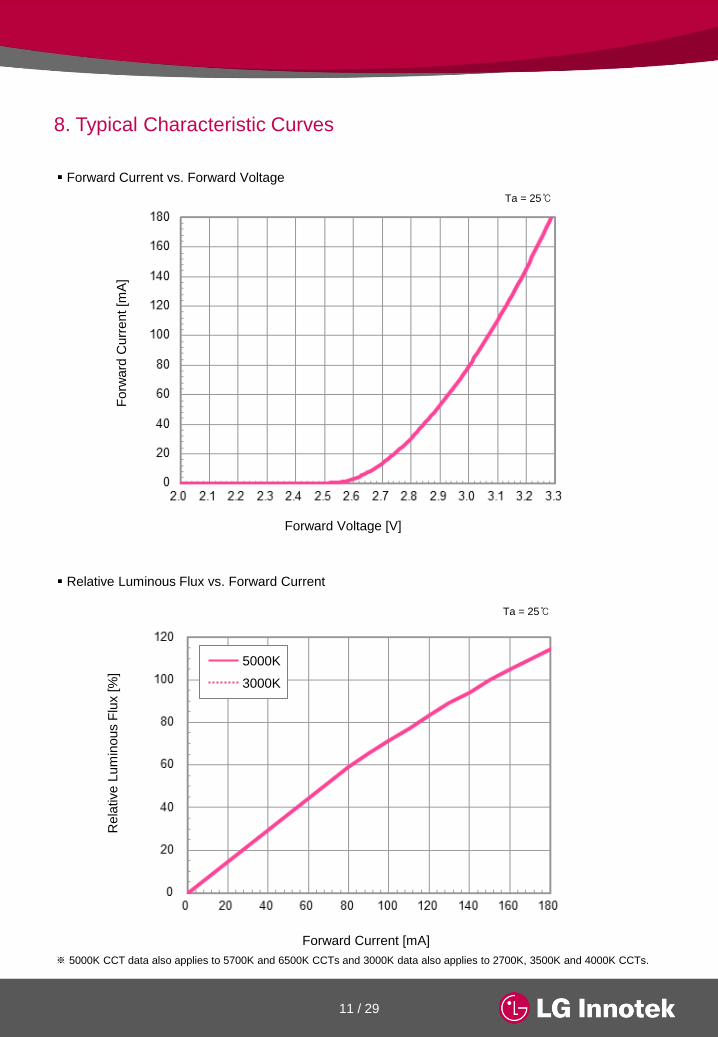
Forward Current vs. Forward Voltage
Forward Voltage [V]
8. Typical Characteristic Curves R
ela
tive L
um
inous F
lux [%
]
Forward Current [mA]
Ta = 25℃
Ta = 25℃
※ 5000K CCT data also applies to 5700K and 6500K CCTs and 3000K data also applies to 2700K, 3500K and 4000K CCTs.
Relative Luminous Flux vs. Forward Current
5000K
3000K

12 / 29
Spectrum
Wavelength [nm]
8. Typical Characteristic Curves
Ta = 25℃, If = 60mA
6500K (F)
Wavelength [nm]
Ta = 25℃, If = 60mA
Rela
tive S
pectr
al P
ow
er
Dis
trib
ution
R
ela
tive S
pectr
al P
ow
er
Dis
trib
ution
5700K (G)
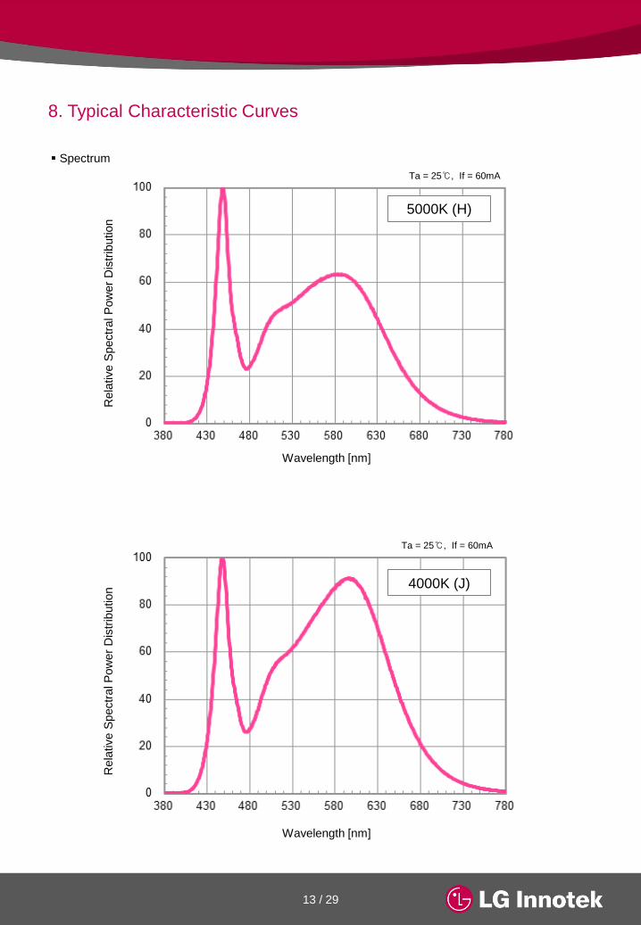
13 / 29
Spectrum
Wavelength [nm]
8. Typical Characteristic Curves
5000K (H)
Wavelength [nm]
4000K (J)
Ta = 25℃, If = 60mA
Ta = 25℃, If = 60mA
Rela
tive S
pectr
al P
ow
er
Dis
trib
ution
R
ela
tive S
pectr
al P
ow
er
Dis
trib
ution

14 / 29
0
20
40
60
80
100
380 430 480 530 580 630 680 730 780
Spectrum
8. Typical Characteristic Curves
Wavelength [nm]
3000K (L)
Ta = 25℃, If = 60mA
Rela
tive S
pectr
al P
ow
er
Dis
trib
ution
R
ela
tive S
pectr
al P
ow
er
Dis
trib
ution
Ta = 25℃, If = 60mA
3500K (K)
Wavelength [nm]

15 / 29
0
20
40
60
80
100
380 430 480 530 580 630 680 730 780
Spectrum
Wavelength [nm]
8. Typical Characteristic Curves
2700K (M)
Ta = 25℃, If = 60mA
Rela
tive S
pectr
al P
ow
er
Dis
trib
ution

16 / 29
Chromaticity Coordinate vs. Forward Current
8. Typical Characteristic Curves
ΔC
hro
maticity
Coord
inate
Forward Current [mA]
ΔC
hro
maticity
Coord
inate
Forward Current [mA]
※ 5000K CCT data also applies to 5700K and 6500K CCTs and 3000K data also applies to 2700K, 3500K and 4000K CCTs.
Ta = 25℃
Cy
Cx
3000K (L)
Cy
Cx
5000K (H)
Ta = 25℃

17 / 29
If = 150mA
8. Typical Characteristic Curves
Radiation Characteristics
Rela
tive L
um
inous F
lux [%
]
Ambient Temperature [℃]
Luminous Flux vs. Temperature
Ta=25℃, If = 60mA
X-X Y-Y
90
0
30
60
-90
-30
-60
0
30
60
90 -90
-30
-60
Ta=25℃, If = 60mA
0 50 100 50 100 0 50 100 50 100
18 / 29
ΔC
hro
maticity
Coord
inate
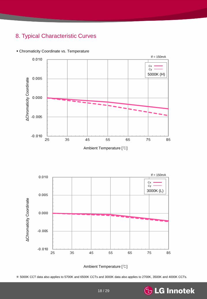
Chromaticity Coordinate vs. Temperature
Ambient Temperature [℃]
8. Typical Characteristic Curves
Ambient Temperature [℃]
Cy
Cx
5000K (H)
If = 150mA
ΔC
hro
maticity
Coord
inate
※ 5000K CCT data also applies to 5700K and 6500K CCTs and 3000K data also applies to 2700K, 3500K and 4000K CCTs.
Cy
Cx
3000K (L)
If = 150mA

19 / 29
Forward Voltage vs. Temperature
Ambient Temperature [℃]
ΔF
orw
ard
Voltage [V
]
If = 150mA
8. Typical Characteristic Curves
※ The ambient temperature values for each graph are obtained with LG Innotek equipment.

20 / 29
9-2. Reliability Tests
9. Reliability Test Items and Conditions
9-1. Failure Criteria
※ All samples are tested using LG Innotek Standard Metal PCB (25x25x1.6 mm3 (L×W×H)) except MSL test .
※ All samples must pass each test item and all test items must be satisfied.
Items Symbol Test Conditions Criteria
Min. Max.
Forward Voltage Vf If = 180mA - Initial Value 1.1
Luminous Flux Φv If = 180mA Initial Value 0.7 -
No Items Test Conditions
Test
Hours
/Cycles
Sample
Size Ac/Re
1 Room Temperature Operating Life
(RTOL) Ta = 25℃, If = 180mA
1,000
Hours 20 pcs 0/1
2 Wet High Temperature Operating Life
(WHTOL)
Ta = 60℃, RH = 90%
If = 180mA
1,000
Hours 20 pcs 0/1
3 High Temperature Operating Life
(HTOL) Ta = 85℃, If = 180mA
1,000
Hours 20 pcs 0/1
4 Low Temperature Operating Life
(LTOL) Ta = -40℃, If = 180mA
1,000
Hours 20 pcs 0/1
5 High Temperature Storage Life
(HTSL) Ta = 100℃
1,000
Hours 20 pcs 0/1
6 Low Temperature Storage Life
(LTSL) Ta = -40℃
1,000
Hours 20 pcs 0/1
7 Wet High Temperature Storage
Life (WHTSL) Ta = 85℃, RH = 85%
1,000
Hours 20 pcs 0/1
8 Temperature Cycle
(TC) -40℃(30min) ~ 100℃(30min)
100
Cycles 20 pcs 0/1
9 Moisture Sensitivity Level
(MSL)
Tsld = 260℃
(Pre treatment 60℃,60%
168 hours)
3 Times 20 pcs 0/1
10 Vibration
100~2000~100Hz
Sweep 4min.
200m/s², 3 directions
48
Minutes 20 pcs 0/1

21 / 29
10-1. Taping Outline Dimensions
10. Packing and Labeling of Product
Polarity
Direction
Anode
Cathode
( End )
Trailer
(Empty Pockets)
(Min. 400mm)
Loaded Pocket
(4,000 pcs)
(1,600mm)
Taping Arrangement
( Start )
Feed Direction
Leader with
Cover Tape
(Min.500mm)
Cover Tape
Embossed Carrier Tape
( Unit : mm )
Packing Materials :
- Reel : Conductive PS (Black)
- Embossed Carrier Tape : Conductive PS (Black)
- Cover Tape : Conductive PET Base
22 / 29
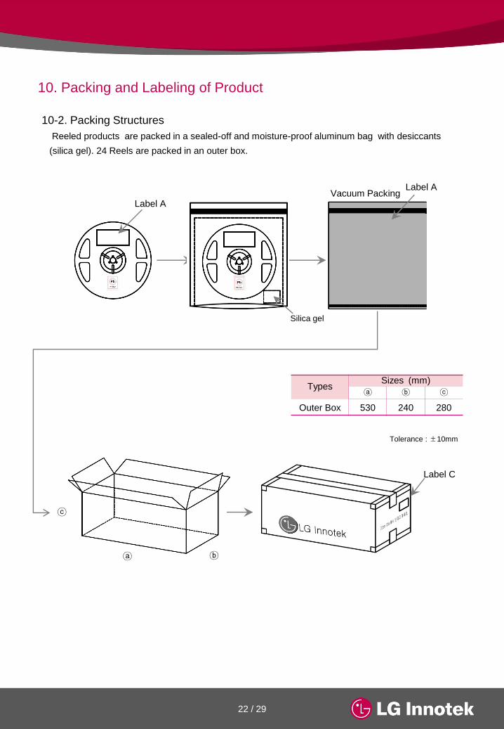
10. Packing and Labeling of Product
10-2. Packing Structures
Reeled products are packed in a sealed-off and moisture-proof aluminum bag with desiccants
(silica gel). 24 Reels are packed in an outer box.
Label A
Label A
Silica gel
Vacuum Packing
Label C
Types Sizes (mm)
ⓐ ⓑ ⓒ
Outer Box 530 240 280
ⓐ ⓑ
ⓒ
Tolerance : ±10mm
23 / 29
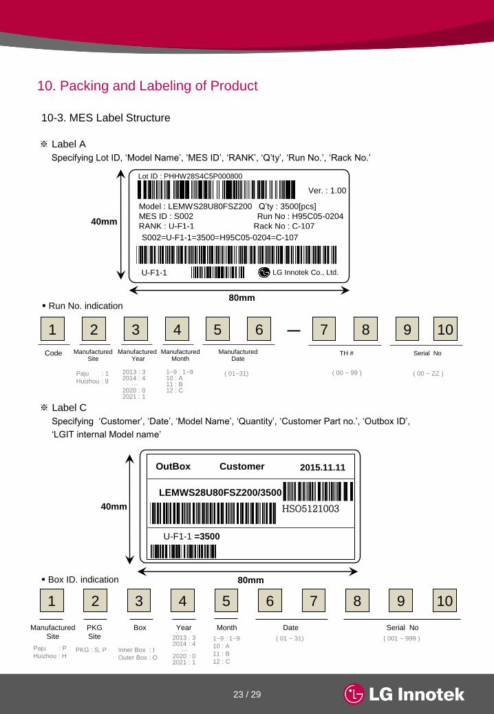
10-3. MES Label Structure
※ Label A
Specifying Lot ID, ‘Model Name’, ‘MES ID’, ‘RANK’, ‘Q’ty’, ‘Run No.’, ‘Rack No.’
Run No. indication
1 2 3 4 5 6
Code
7 8 9
Serial No Manufactured Year
Manufactured Month
Manufactured Date
Manufactured Site
( 00 ~ ZZ ) ( 01~31)
10
Paju : 1
Huizhou : 9
1~9 : 1~9 10 : A 11 : B 12 : C
2013 : 3 2014 : 4 ··· 2020 : 0 2021 : 1
TH #
( 00 ~ 99 )
Box ID. indication
1 2 3 4 5
Manufactured
Site
9
Serial No Box Date
( 01 ~ 31) ( 001 ~ 999 )
10 6 7 8
1~9 : 1~9
10 : A
11 : B
12 : C
PKG
Site
Month Year
Paju : P
Huizhou : H PKG : S, P Inner Box : I
Outer Box : O
2013 : 3 2014 : 4 ··· 2020 : 0 2021 : 1
※ Label C
Specifying ‘Customer’, ‘Date’, ‘Model Name’, ‘Quantity’, ‘Customer Part no.’, ‘Outbox ID’,
‘LGIT internal Model name’
10. Packing and Labeling of Product
Lot ID : PHHW28S4C5P000800
Model : LEMWS28U80FSZ200 Q’ty : 3500[pcs]
MES ID : S002 Run No : H95C05-0204
RANK : U-F1-1 Rack No : C-107
Ver. : 1.00
S002=U-F1-1=3500=H95C05-0204=C-107
P-J21-2
80mm
40mm
LG Innotek Co., Ltd. U-F1-1
OutBox Customer 2015.11.11
HSO5121003
80mm
LEMWS28U80FSZ200/3500
U-F1-1 =3500
40mm

24 / 29
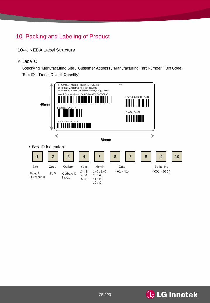
10-4. NEDA Label Structure
※ Label A
Specifying ‘Manufacturing Part Number’, ‘Quantity’, ‘Bin Code’, ‘Lot’, ‘Date Code’
and ‘Country of Origin’
Date Code(9D)
1 2 3 4
Year
01~99
Week
01~52
Lot#(1T)
LG Innotek Trace Code
Manuf Part Number (1P): LEMWS28U80GSZ2A0
80mm
40mm
Date Code(9D): 1222
Lot#(1T): DPMWY5K25VP003900
Qty(Q): 3500 Bin Code: U–G5–0
LG Innotek
Country of CN
Origin (4L)
10. Packing and Labeling of Product
Bin Code
1 2 1 2
Flux Color Coordinates
3 1 2
Forward Voltage
25 / 29
10-4. NEDA Label Structure
Box ID indication
1 2 3 4 5
Site
9
Serial No Outbox Date
( 01 ~ 31) ( 001 ~ 999 )
10 6 7 8
1~9 : 1~9
10 : A
11 : B
12 : C
Code Month Year
13 : 3
14 : 4
15 : 5
Outbox: O
Inbox: I
Paju: P
Huizhou: H S, P
※ Label C
Specifying ‘Manufacturing Site’, ‘Customer Address’, ‘Manufacturing Part Number’, ‘Bin Code’,
‘Box ID’, ‘Trans ID’ and ‘Quantity’
10. Packing and Labeling of Product
40mm
Manuf Part Number (1P): LEMWS28U80FSZ2A0
Qty(Q): 84000
Bin Code: U-G5-0
Trans ID (K): IAP5X8
BOX ID: HSO2531048
FROM: LG Innotek(HuiZhou)Co., Ltd
District 18,ZhongKai Hi-Tech Industry
Development Zone, Huizhou ,Guangdong, China
TO:
80mm
26 / 29
11. Cautions on Use
11-1. Moisture-Proof Package
-. The moisture in the SMD package may vaporize and expand during soldering.
-. The moisture can damage the optical characteristics of the LEDs due to the encapsulation.
11-2. During Storage
11-3. During Usage
-. The LED should avoid the direct contact with hazardous materials such as sulfur, chlorine, phthalate,
etc..
-. The metal parts on the LED can rust when exposed to corrosive gases. Therefore, exposure to
corrosive gases must be avoided during operation and storage.
-. The silver-plated metal parts also can be affected not only by the corrosive gases emitted inside of
the end-products but by the gases penetrated from outside environment.
-. Extreme environments such as sudden ambient temperature changes or high humidity that can
cause condensation must be avoided.
11-4. Cleaning
-. Do not use brushes for cleaning or organic solvents (i.e. Acetone, TCE, etc..) for washing as
they may damage the resin of the LEDs.
-. Isopropyl Alcohol (IPA) is the recommended solvent for cleaning the LEDs under the following
conditions.
Clearing Condition : IPA, 25℃ max. × 60 sec max.
-. Ultrasonic cleaning is not recommended.
-. Pretests should be conducted with the actual cleaning process to validate that the process will not
damage the LEDs.
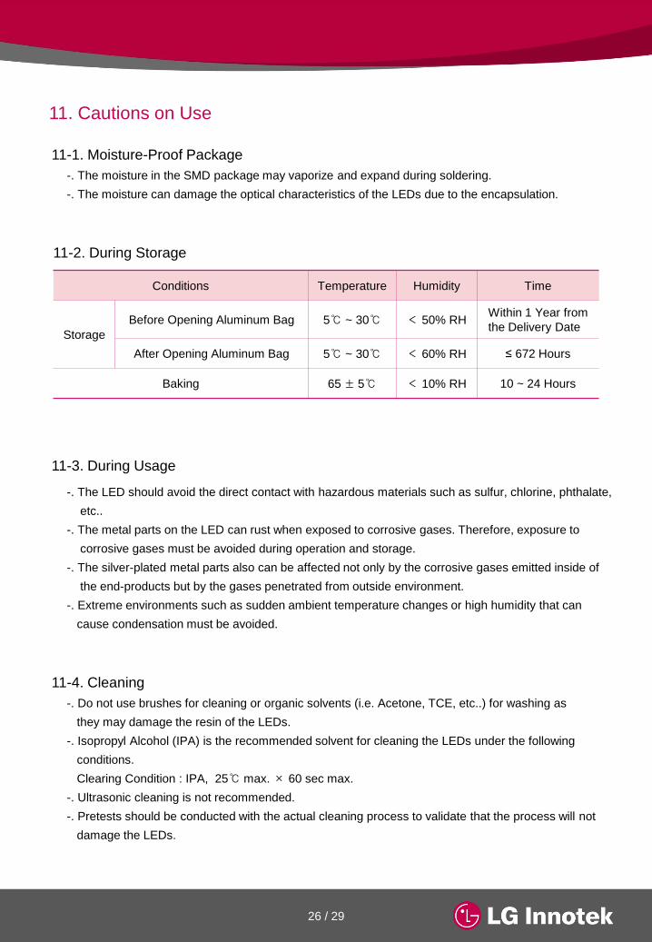
Conditions Temperature Humidity Time
Storage
Before Opening Aluminum Bag 5℃ ~ 30℃ < 50% RH Within 1 Year from
the Delivery Date
After Opening Aluminum Bag 5℃ ~ 30℃ < 60% RH ≤ 672 Hours
Baking 65 ± 5℃ < 10% RH 10 ~ 24 Hours
27 / 29
11. Cautions on Use
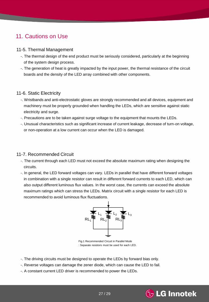
Fig.1 Recommended Circuit in Parallel Mode
: Separate resistors must be used for each LED.
L1
RL1
L2 L3
RL2 RL3
11-5. Thermal Management
-. The thermal design of the end product must be seriously considered, particularly at the beginning
of the system design process.
-. The generation of heat is greatly impacted by the input power, the thermal resistance of the circuit
boards and the density of the LED array combined with other components.
11-6. Static Electricity
-. Wristbands and anti-electrostatic gloves are strongly recommended and all devices, equipment and
machinery must be properly grounded when handling the LEDs, which are sensitive against static
electricity and surge.
-. Precautions are to be taken against surge voltage to the equipment that mounts the LEDs.
-. Unusual characteristics such as significant increase of current leakage, decrease of turn-on voltage,
or non-operation at a low current can occur when the LED is damaged.
11-7. Recommended Circuit
-. The current through each LED must not exceed the absolute maximum rating when designing the
circuits.
-. In general, the LED forward voltages can vary. LEDs in parallel that have different forward voltages
in combination with a single resistor can result in different forward currents to each LED, which can
also output different luminous flux values. In the worst case, the currents can exceed the absolute
maximum ratings which can stress the LEDs. Matrix circuit with a single resistor for each LED is
recommended to avoid luminous flux fluctuations.
-. The driving circuits must be designed to operate the LEDs by forward bias only.
-. Reverse voltages can damage the zener diode, which can cause the LED to fail.
-. A constant current LED driver is recommended to power the LEDs.
28 / 29
11. Cautions on Use
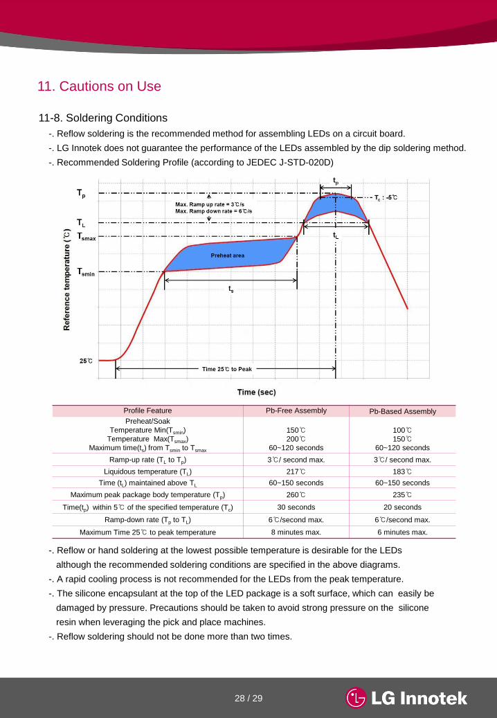
11-8. Soldering Conditions
-. Reflow soldering is the recommended method for assembling LEDs on a circuit board.
-. LG Innotek does not guarantee the performance of the LEDs assembled by the dip soldering method.
-. Recommended Soldering Profile (according to JEDEC J-STD-020D)
-. Reflow or hand soldering at the lowest possible temperature is desirable for the LEDs
although the recommended soldering conditions are specified in the above diagrams.
-. A rapid cooling process is not recommended for the LEDs from the peak temperature.
-. The silicone encapsulant at the top of the LED package is a soft surface, which can easily be
damaged by pressure. Precautions should be taken to avoid strong pressure on the silicone
resin when leveraging the pick and place machines.
-. Reflow soldering should not be done more than two times.
Profile Feature Pb-Free Assembly Pb-Based Assembly
Preheat/Soak
Temperature Min(Tsmin)
Temperature Max(Tsmax)
Maximum time(ts) from Tsmin to Tsmax
150℃
200℃
60~120 seconds
100℃
150℃
60~120 seconds
Ramp-up rate (TL to Tp) 3℃/ second max. 3℃/ second max.
Liquidous temperature (TL) 217℃ 183℃
Time (tL) maintained above TL 60~150 seconds 60~150 seconds
Maximum peak package body temperature (Tp) 260℃ 235℃
Time(tp) within 5℃ of the specified temperature (Tc) 30 seconds 20 seconds
Ramp-down rate (Tp to TL) 6℃/second max. 6℃/second max.
Maximum Time 25℃ to peak temperature 8 minutes max. 6 minutes max.
29 / 29
11. Cautions on Use
11-9. Soldering Iron
-. The recommended condition is less than 5 seconds at 260℃.
-. The time must be shorter for higher temperatures. (+10℃ → -1sec).
-. The power dissipation of the soldering iron should be lower than 15W and the surface temperature
of the device should be controlled at or under 230℃.
11-10. Eye Safety Guidelines
-. Do not directly look at the light when the LEDs are on.
-. Proceed with caution to avoid the risk of damage to the eyes when examining the LEDs with
optical instruments.
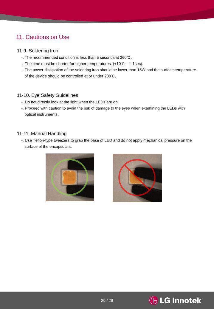
11-11. Manual Handling
-. Use Teflon-type tweezers to grab the base of LED and do not apply mechanical pressure on the
surface of the encapsulant.
30 / 29
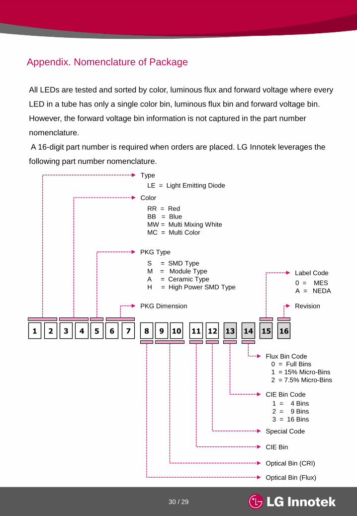
1 3 4 6 7 8 10 2 9 5 11 12
CIE Bin Code
13 14 15 16
1 = 4 Bins
2 = 9 Bins
3 = 16 Bins
Flux Bin Code
Label Code
RR = Red
BB = Blue
MW = Multi Mixing White
MC = Multi Color
Type
LE = Light Emitting Diode
Color
PKG Type
S = SMD Type
M = Module Type
A = Ceramic Type
H = High Power SMD Type
PKG Dimension Revision
Optical Bin (Flux)
Optical Bin (CRI)
CIE Bin
Special Code
All LEDs are tested and sorted by color, luminous flux and forward voltage where every
LED in a tube has only a single color bin, luminous flux bin and forward voltage bin.
However, the forward voltage bin information is not captured in the part number
nomenclature.
A 16-digit part number is required when orders are placed. LG Innotek leverages the
following part number nomenclature.
0 = MES
A = NEDA
0 = Full Bins
1 = 15% Micro-Bins
2 = 7.5% Micro-Bins
Appendix. Nomenclature of Package
31 / 29
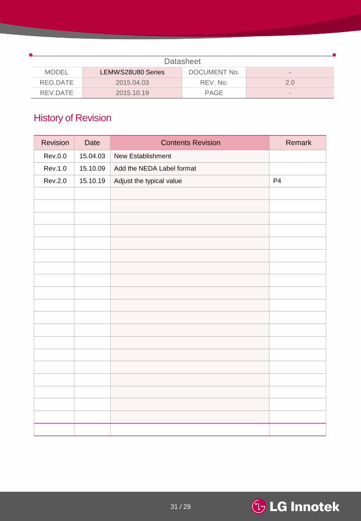
Datasheet
MODEL LEMWS28U80 Series DOCUMENT No. -
REG.DATE 2015.04.03 REV. No. 2.0
REV.DATE 2015.10.19 PAGE -
Revision Date Contents Revision Remark
Rev.0.0 15.04.03 New Establishment
Rev.1.0 15.10.09 Add the NEDA Label format
Rev.2.0 15.10.19 Adjust the typical value P4
History of Revision


![Acrich MJT 5050 Series - seoulsemicon.comSpecification]SAW0L60A_R3.0_1712.pdf · 0.3373 0.3534 0.3293 0.3384 0.3369 0.3451 C0 C1 C2 CIE x CIE y CIE x CIE y CIE x CIE y 0.3376 0.3616](https://img.pdfslide.net/doc/110x75/5bf955f609d3f2ab7d8cc0ef/acrich-mjt-5050-series-specificationsaw0l60ar301712pdf-03373-03534.jpg)