Embed Size (px)
Citation preview

To: Digi-Key Issue No. : EZJ08022901Date of Issue :
Classification : New Changed
: MULTILAYER VARISTOR , CHIP TYPE: EZJP0V080MAEZJP0V080KA
EZJP0V080GA
:: Japan: Consumer Type Electric Equipment
※If you approve this specification, please fill in and sign the below and return 1copy to us.
:
:
:
(signature)::
Prepared by : Engineering Section
Capacitor Business Unit Phone : +81-123-23-8149 (Direct)Panasonic Electronic Devices Co.,Ltd. Fax : +81-123-22-1261 (Direct)25.Kohata-nishinaka..Uji City , Kyoto, Japan
Contact Person : Y.Sasaki Title : Engineer
Phone : +81-774-32-1111(Representative)Authorized by : Y.Sakaguti Title : Manager of Engineering
If there is a question, please ask the engineering section about it directly.
Approval Date
Excecuted by
TitleDept.
PRODUCT SPECIFICATION FOR APPROVAL
February 29.2008
Product Description Product Part Number
Customers Part Number Country of Origin Applications
Approval No
DESIGN
Y.Sasaki
CLASSIFICATION No.
SUBJECT PAGE
DATE
151S-EZJ-KPB357E
Multilayer Varistor,Chip Type EIA:0402size Individual Specification EZJP0V080□A
1 of 1
28 Feb, 2008
SPECIFICATIONS
APPROVAL
Y.Sakaguti
CHECK T.Kawamura
Note ;
Panasonic Electronic Devices Co., Ltd.
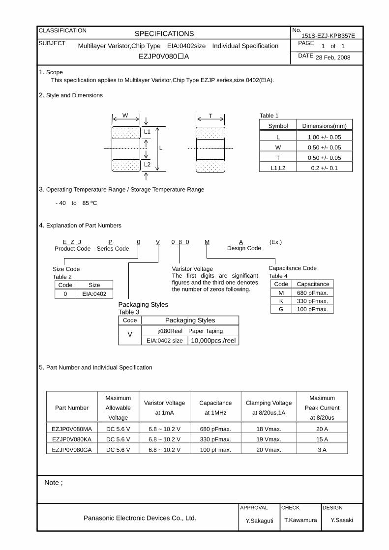
1. Scope This specification applies to Multilayer Varistor,Chip Type EZJP series,size 0402(EIA).
2. Style and Dimensions
Table 1
Symbol Dimensions(mm)
L 1.00 +/- 0.05
W 0.50 +/- 0.05
T 0.50 +/- 0.05
L1,L2 0.2 +/- 0.1 3. Operating Temperature Range / Storage Temperature Range
- 40 to 85 ºC 4. Explanation of Part Numbers
E Z J P 0 V 0 8 0 M A (Ex.)
5. Part Number and Individual Specification
Part Number
Maximum
Allowable
Voltage
Varistor Voltage
at 1mA
Capacitance
at 1MHz
Clamping Voltage
at 8/20us,1A
Maximum
Peak Current
at 8/20us
EZJP0V080MA DC 5.6 V 6.8 ~ 10.2 V 680 pFmax. 18 Vmax. 20 A
EZJP0V080KA DC 5.6 V 6.8 ~ 10.2 V 330 pFmax. 19 Vmax. 15 A
EZJP0V080GA DC 5.6 V 6.8 ~ 10.2 V 100 pFmax. 20 Vmax. 3 A
L
L1
L2
W T
Product Code
Packaging Styles Table 3
Code Packaging Styles
φ180Reel Paper Taping V EIA:0402 size 10,000pcs./reel
Varistor Voltage The first digits are significant figures and the third one denotes the number of zeros following.
Design Code
Size Code Table 2
Code Size 0 EIA:0402
Series Code
Capacitance Code Table 4
Code CapacitanceM 680 pFmax.K 330 pFmax.G 100 pFmax.
1 of 5
28 Feb,2008
Note ;
CLASSIFICATION SPECIFICATIONS No.
SUBJECT PAGE
DATE
151S-EZJ-KPG357E
Multilayer Varistor , Chip Type Common Specification(EZJP Series)
1. Information 1- 1.Applicable laws and regulations
(1) Any ozone-depleting substances listed in the Montreal Protocol are not used in the manufacturing processes for parts and materials used in this product.
(2) PBB and PBDE are intentionally excluded from materials used in this product. (3) All the materials used in this product are registered materials under the Law Concerning Examination and
Regulation of Manufacture and Handling of Chemical Substances. (4) This product complies with the RoHS, DIRECTIVE 2002/95/EC on the Restriction of the use of certain Hazard-
ous Substances in electrical and electronic equipment. (5) This product is exported with export procedures under export related laws and regulations such as the Foreign
Exchange and Foreign Trade Law.
1- 2.Limitation in Applications This product was designed and manufactured for general-purpose electronic equipment such as household, office,
information & communication equipment. When the following applications, which are required higher reliability and safety because the trouble or malfunction of this product may threaten the lives and/or properties, are examined, separate specifications suitable for the application should be exchanged.
・Aerospace / Aircraft equipment, Warning / Antitheft equipment, Medical equipment, Transport equipment (Motor vehicles, Trains, Ship and Vessel ), Highly public information processing equipment, Others equivalent to the above.
1- 3.Production factory
(1) Panasonic Electronic Devices Hokkaido Co., Ltd. (2) Panasonic Electronic Devices (Tianjin) Co., Ltd. (PEDTJ)
2. Scope 2- 1.This specification applies common specification to multilayer varistor/chip type .If there is a difference between this
common specification and any individual specifications, priority shall be given to the individual specifications. 2- 2.This product shall be used for general-purpose electronic equipment such as audiovisual, household, office, informa-
tion & communication equipment. Unreasonable applications may accelerate performance deterioration or short/open circuits as failure modes affect-ing the life end.Adequate safety shall be ensured especially for product design required a high level of safety with the following considerations.
1) Previously examine how a single trouble in this product affects the end product. 2) Design a protection circuit as Failsafe-design to avoid unsafe system resulting from a single trouble with this
product. Whenever a doubt about safety arises from this product, immediately inform us for technical consultation without fail, please.
2-3.This specification is a part of contract documents pertaining to the trade made by and between your company and Matsushita Electric Industrial Co., Ltd.
2-4.The change of product specification for approval and the change influenced performance, quality and environment is determined on prior consultation.
3. Part Number Code
1 2 3 4 5 6 7 8 9 10 11 12 E Z J P 0 V 0 8 0 M A (1) (2) (3) (4) (5) (6) (7) (8)
3- 1.Common Code (1) EZJ : Multilayer Varistor , Chip Type
3- 2.Series Code(2) P:EZJP series
2 of 5
28 Feb,2008
Note ;
CLASSIFICATION SPECIFICATIONS No.
SUBJECT PAGE
DATE
151S-EZJ-KPG357E
Multilayer Varistor , Chip Type Common Specification(EZJP Series)
3- 3.Size Code(3) 0:0402(EIA) 1:0603(EIA) 3- 4.Packaging Styles Code(4)
Shown in Individual Specification. 3- 5.Varistor voltage (5)
The first two digits are significant figures and third one denotes the number of zeros following. 3- 6.Capacitance Code (6)
A:3 pF R:20 pF D:27pF E:47 pF W:56 pF F:68 pF G:100 pF H:150 pF J:220 pF K:330 pF M:680 pF ※ 3 pF or less are displayed a top 2 figures using 10 or 11 figures. For example 2.0 pF : 20 1.5 pF : 15
3- 7.Design Code (7) A specific code shall be given for identification as individual specification or design ranking if necessary. 3- 8.Special Code(8)
A specific code shall be given for identification as individual specification or design ranking if necessary.
None Capacitance Tolerance : max. B Capacitance Tolerance : +/- 0.10 pF
C Capacitance Tolerance : +/- 0.25 pF D Capacitance Tolerance : +/- 0.50 pF K Capacitance Tolerance : +/- 10 %
M Capacitance Tolerance : +/- 20 %
4. Operating Temperature Range / Storage Temperature Range Shown in Individual Specification.
5. Test Unless otherwise specified, all tests and measurements shall be made at a temperature of 15 to 35℃ and at a relative humidity of 45 to 75%. If results obtained are doubted, a further test should be carried out at a temperature of 20 +/- 2℃ and a relative humid-ity of 60 to 70%.
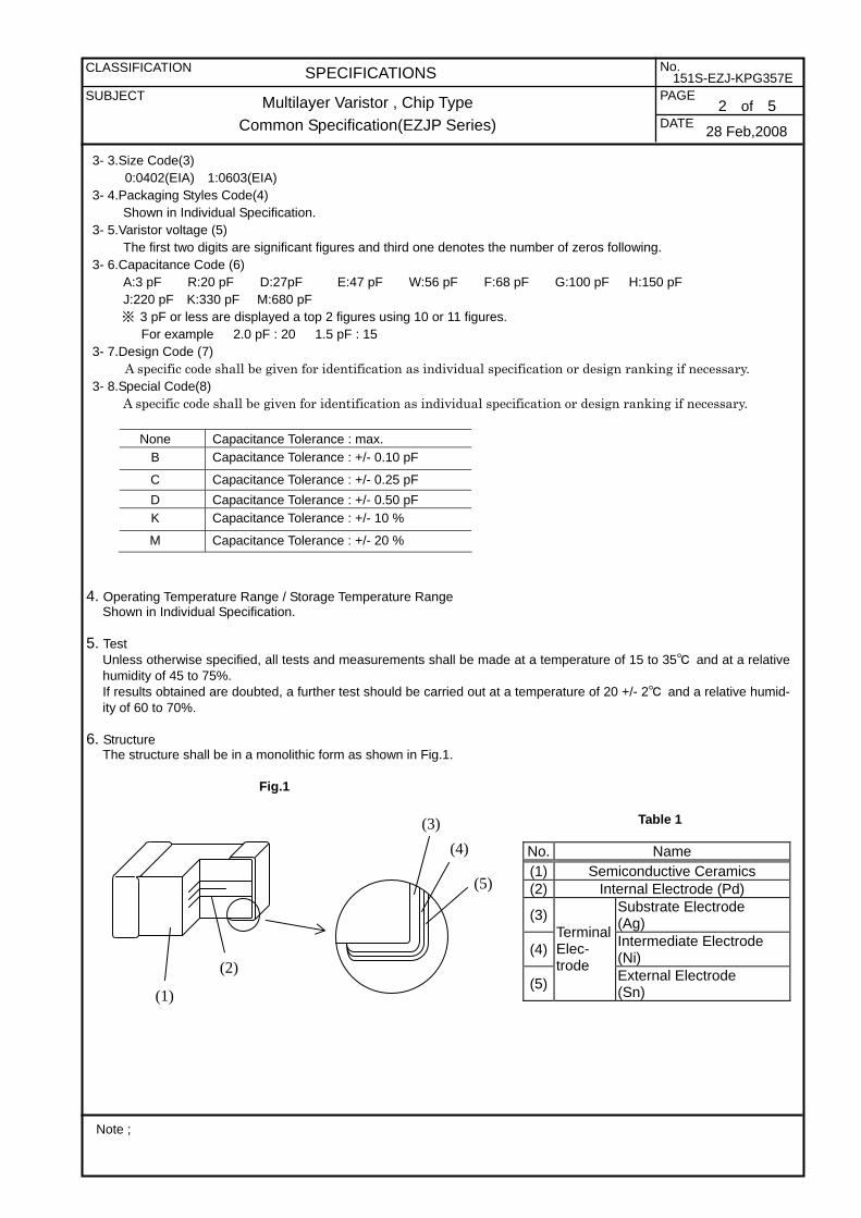
6. Structure
The structure shall be in a monolithic form as shown in Fig.1.
Fig.1
Table 1
No. Name (1) Semiconductive Ceramics (2) Internal Electrode (Pd)
(3) Substrate Electrode (Ag)
(4) Intermediate Electrode (Ni)
(5)
Terminal Elec-trode
External Electrode (Sn)
(1)
(2)
(3)(4)
(5)

3 of 5
28 Feb,2008
CLASSIFICATION SPECIFICATIONS No.
SUBJECT PAGE
DATE
151S-EZJ-KPG357E
Multilayer Varistor , Chip Type Common Specification(EZJP Series)
Note ;
Table 2 No Contents Performance Test Method 1 Appearance There shall be no defects which affect
the life and use. With a magnifying glass (3 times).
2 Dimensions Shown in Individual Specification. With slide calipers and a micrometer.
3 Maximum allowable voltage
Shown in Individual Specification. The maximum DC voltage that can be applied continuously in the specified operating tem-perature.
4 Varistor voltage Shown in Individual Specification. The voltage between two terminals with the specified measuring current CmA DC applied is called Vc or Vc mA. The measurement shall be made as fast as possible to avoid heat af-fection.
5 Capacitance Shown in Individual Specification. Our Measurement instrument is shown in the Table 3
6 Clamping voltage Shown in Individual Specification. The maximum voltage between two terminals with the specified impulse current(8/20 us).
7
Maximum peak current
Shown in Individual Specification. The maximum current at less than +/-10 % of varistor voltage change when impulse cur-rent(8/20 us) is applied two times continuously with the interval of 5 minutes.
8 Maximum ESD Shown in Individual Specification. The maximum ESD within the varistor voltage change of +/-30 % when impressing 10 times of ESD(five times of positive-negative for each polarity) which is based on IEC61000-4-2.
9 Bending strength
Appear-ance
There shall be no cracks and other mechanical damage.
After soldering capacitor on the substrate 1 mm of bending shall be applied for 5 seconds. Bending speed : 1 mm/s (shown in Fig. 2)
10
Solderability More than 75 % of the soldered area of both terminal electrodes shall be covered with fresh solder.
Solder temperature : 230+/-5 °C Dipping period : 4+/-1 s Dip the specimen in solder so that both termi-nal electrodes are completely submerged. Use solder H63A(JIS-Z-3282). For the flux use rosin (JIS-K-5902) of ethanol solution of a concentration of about 25% by weight. Use tweezers for the holder to dip the speci-men.
(continue)
Measuring Frequency
Measuring Voltage
1 MHz +/-10 % 1.0 +/-0.5 Vrms

4 of 5
28 Feb,2008
CLASSIFICATION SPECIFICATIONS No.
SUBJECT PAGE
DATE
151S-EZJ-KPG357E
Multilayer Varistor , Chip Type Common Specification(EZJP Series)
Note ;
Table 2
No Contents Performance Test Method Appear-ance
There shall be no cracks and other mechanical damage.
11
Resistance to solder heat
Varistor voltage
dVc/Vc : Within +/- 10.0 %
Solder temperature : 270+/-5 °C Dipping period : 3 +/-0.5 s Dipping position : Up to the positioin in which
both terminal hides com-pletely.
Use solder H63A(JIS-Z-3282). For the flux use rosin (JIS-K-5902) of ethanol solution of a concentration of about 25 % by weight. Use tweezers for the holder to dip the specimen.
Appear-ance
There shall be no cracks and other mechanical damage. dVc/Vc : Within +/- 10.0 %
Solder the specimen to the testing jig shown in Fig.1. Condition the specimen to each tem-perature from step 1 to 4 in this order for the period shown in the table below. Regarding this conditioning as one cycle, per-form 5 cycles continuously.
12 Tempera-ture cycle
Varistor voltage
Appear-ance
There shall be no cracks and other mechanical damage.
13
Damp Heat Laod (Moisture Resistant Loading)
Varistor voltage
dVc/Vc : Within +/- 10.0 %
The specimen shall be subjected to specified conditions and then stored at room tempera-ture and normal humidity for 1 to 2 hours. Thereafter,the change of V shall be measured.
Test temperature : 40 +/-2 °C Relative humidity : 90 to 95 % Laod : Maximum allowable voltage Test period : 500 +24/0 h
Appear-ance
There shall be no cracks and other mechanical damage.
14 High Tem-perature Laod (High Tem-perature Resistant Loading)
Varistor voltage
dVc/Vc : Within +/- 10.0 %
The specimen shall be subjected to specified conditions and then stored at room tempera-ture and normal humidity for 1 to 2 hours. Thereafter,the change of V shall be measured.
Test temperature : 125 +/-3 °C Laod : Maximum allowable voltage Test period : 1000 +24/0 h
Step Temperature (°C)
Period (min.)
1 Minimum operation temperature +/- 3 30 +/-3
2 Room temperature 3 max.
3 Maximum operation temperature +/-5 30 +/-3
4 Room temperature 3 max.
Order Temperature(°C) Period (S)
1 80 to 100 120 to 180
2 150 to 200 120 to 180

5 of 5
28 Feb,2008
CLASSIFICATION SPECIFICATIONS No.
SUBJECT PAGE
DATE
151S-EZJ-KPG357E
Multilayer Varistor , Chip Type Common Specification(EZJP Series)
Note ;
When uncertainty occurs in the weather resistance characteristic tests (temperature cycle, moisture resistance, moisture resistant loading, high temperature resistant loading), the same tests shall be performed for the capacitor it-self.
Table 3 Our Measurement instrument
Measuring Instrument 4278A 1kHz/1MHz Capacitance Meter (Agilent Technologies)
Measuring mode Parallel Mode
Recommended measuring jig 16034E Test Fixture (Agilent Technologies)
Fig. 1 Testing jig
Table 4 Size (EIA) A B C
0402 0.5 1.5 0.6
0603 1.0 3.0 1.2
Unit : mm
Material : Glass epoxy board
Material : Glass epoxy board Thickness : 1.6mm
:Copper foil (0.035mm thick) :Solder resist
Fig. 2 Testing jig
Table 5 Type (EIA) A B C
BoardThickness
0402 0.5 1.5 0.6 0.6
0603 1.0 3.0 1.2 1.6
Unit : mm
Material : Glass epoxy board :Copper foil (0.035mm thick)
:Solder resist

1 of 8
5 June, 2006
DESIGN
Y.Sasaki
CLASSIFICATION No.
SUBJECT PAGE
DATE
151S-EZJ-SCS002E
Multilayer Varistor , Chip Type Common Specification ( Precautions for Use)
APPROVAL
Y.Sakaguti
CHECK T.Kawamura
Note ;
Panasonic Electronic Devices Co., Ltd.
SPECIFICATIONS
1. Precautions for Use
The Multilayer Varistors (hereafter refereed to as “The Varistors”) are intended for general purpose applications as countermeasures against ESD and noise that can occur in consumer electronics (audio/visual, home, office, information & communication) equipment. The Varistors may fail in a short circuit mode or in an open-circuit mode, when subjected to severe conditions of electrical, environmental and/or mechanical stress beyond the specified “Ratings” and “Conditions” in the catalog. If it is used especially in the short state, there is a afraid that a circuit board may be damaged by fire by generation of heat by short current. For products which require high safety levels, please carefully consider how a single malfunction can affect your product. Please examine a protection means to intercept short current. The Varistors may fail in a short circuit mode in an open-circuit mode when subjected to severe conditions of electrical, environmental and/or mechanical stress beyond the specified “Rating and specified “Conditions” in the Specifications, resulting in burn out, flaming or glowing in the worst case.
2. Operating Conditions and Circuit Design 2- 1.Circuit Design
2-1-1. Operating Temperature and Storage Temperature The specified “Operating Temperature Range” in the Specifications is the absolute maximum and minimum temperature rating. Every circuit mounting a Varistor shall be operated within the specified “Operating Temperature Range”. The Varistors mounted on PCB shall be stored without operating within the specified “Storage Temperature Range” in the Specifications.
2-1-2. Design of Voltage Application The Varistors shall not be operated exceeding the specified “Maximum Allowable Voltage” in the Specification. If the Varistors are operated beyond the specified Maximum allowable voltage, it may cause a short circuit and/or damage due to thermal run away. If high frequency voltage or fast rising pulse voltage is applied continuously even within the “Rated Voltage”, contact our engineering section before use. Such continuous application affects the life of the Varistors.
2-1-3. Self-heating
The surface temperature of the Varistors shall be under the specified Maximum Operating Temperature in the Specifications including the temperature rise caused by self-heating. Check the temperature rise of the Varistor in your circuit.
2-1-4. Environmental Restrictions The Varistors shall not be operated and / or stored under the following environmental conditions. (1) Environmental conditions
(a) Under direct exposure to water or salt water. (b) Under conditions where water can condense and/or dew can form. (c) Under conditions containing corrosive gases such as hydrogen sulfide, sulfurous acid, chlorine
and ammonia. (2) Mechanical conditions
Under severe conditions of vibration or impact beyond the specified conditions in the Specifications.
2 of 8
5 June, 2006
CLASSIFICATION No.
SUBJECT PAGE
DATE
151S-EZJ-SCS002E
Multilayer Varistor , Chip Type Common Specification ( Precautions for Use)
SPECIFICATIONS
Note ;
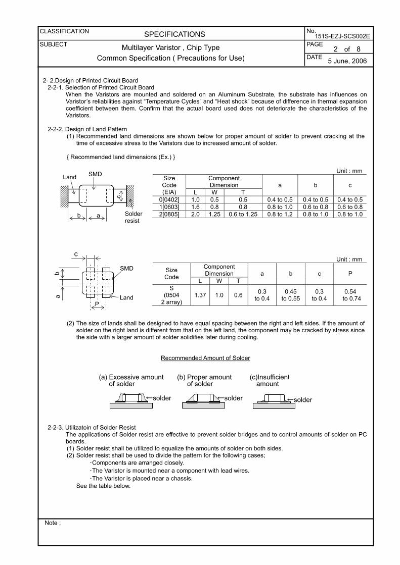
2- 2.Design of Printed Circuit Board
2-2-1. Selection of Printed Circuit Board When the Varistors are mounted and soldered on an Aluminum Substrate, the substrate has influences on Varistor’s reliabilities against “Temperature Cycles” and “Heat shock” because of difference in thermal expansion coefficient between them. Confirm that the actual board used does not deteriorate the characteristics of the Varistors.
2-2-2. Design of Land Pattern
(1) Recommended land dimensions are shown below for proper amount of solder to prevent cracking at the time of excessive stress to the Varistors due to increased amount of solder.
{ Recommended land dimensions (Ex.) }
Unit : mm Component Dimension
Size Code (EIA) L W T
a b c
0[0402] 1.0 0.5 0.5 0.4 to 0.5 0.4 to 0.5 0.4 to 0.51[0603] 1.6 0.8 0.8 0.8 to 1.0 0.6 to 0.8 0.6 to 0.82[0805] 2.0 1.25 0.6 to 1.25 0.8 to 1.2 0.8 to 1.0 0.8 to 1.0
Unit : mm Component Dimension Size
Code L W T a b c P
S (0504
2 array) 1.37 1.0 0.6 0.3
to 0.4 0.45
to 0.55 0.3
to 0.4 0.54
to 0.74
(2) The size of lands shall be designed to have equal spacing between the right and left sides. If the amount of solder on the right land is different from that on the left land, the component may be cracked by stress since the side with a larger amount of solder solidifies later during cooling.
Recommended Amount of Solder
2-2-3. Utilizatoin of Solder Resist
The applications of Solder resist are effective to prevent solder bridges and to control amounts of solder on PC boards. (1) Solder resist shall be utilized to equalize the amounts of solder on both sides. (2) Solder resist shall be used to divide the pattern for the following cases;
・Components are arranged closely. ・The Varistor is mounted near a component with lead wires. ・The Varistor is placed near a chassis.
See the table below.
(a) Excessive amount of solder
(b) Proper amount of solder
(c)Insufficient amount
←solder ←solder ←solder
a b Solder resist
SMD Land
c
P
c
a b
Land
SMD
3 of 8
5 June, 2006
CLASSIFICATION No.
SUBJECT PAGE
DATE
151S-EZJ-SCS002E
Multilayer Varistor , Chip Type Common Specification ( Precautions for Use)
SPECIFICATIONS
Note ;
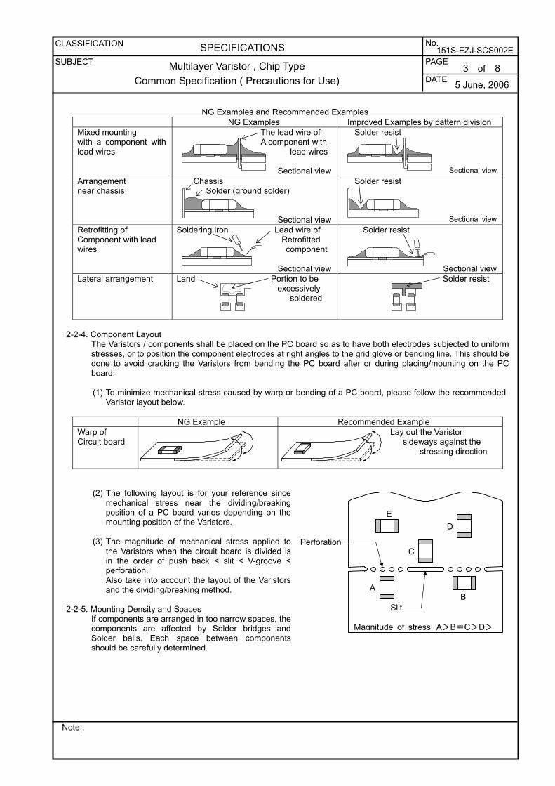
NG Examples and Recommended Examples
NG Examples Improved Examples by pattern division Mixed mounting with a component with lead wires
The lead wire of A component with lead wires
Sectional view
Solder resist
Sectional viewArrangement near chassis
Chassis Solder (ground solder)
Sectional view
Solder resist
Sectional viewRetrofitting of Component with lead wires
Soldering iron Lead wire of Retrofitted component
Sectional view
Solder resist
Sectional viewLateral arrangement Land Portion to be
excessively soldered
Solder resist
2-2-4. Component Layout
The Varistors / components shall be placed on the PC board so as to have both electrodes subjected to uniform stresses, or to position the component electrodes at right angles to the grid glove or bending line. This should be done to avoid cracking the Varistors from bending the PC board after or during placing/mounting on the PC board.
(1) To minimize mechanical stress caused by warp or bending of a PC board, please follow the recommended
Varistor layout below.
NG Example Recommended Example Warp of Circuit board
Lay out the Varistor sideways against the stressing direction
(2) The following layout is for your reference since mechanical stress near the dividing/breaking position of a PC board varies depending on the mounting position of the Varistors.
(3) The magnitude of mechanical stress applied to
the Varistors when the circuit board is divided is in the order of push back < slit < V-groove < perforation. Also take into account the layout of the Varistors and the dividing/breaking method.
2-2-5. Mounting Density and Spaces
If components are arranged in too narrow spaces, the components are affected by Solder bridges and Solder balls. Each space between components should be carefully determined.
AB
C
ED
Slit
Magnitude of stress A>B=C>D>
Perforation

4 of 8
5 June, 2006
CLASSIFICATION No.
SUBJECT PAGE
DATE
151S-EZJ-SCS002E
Multilayer Varistor , Chip Type Common Specification ( Precautions for Use)
SPECIFICATIONS
Note ;
3. Precautions for Assembly 3- 1.Storage
(1) The Varistors before mounting on PCB shall be stored between 5 - 40°C and 20 - 70% RH, not under severe conditions of high temperature and humidity.
(2) If stored in a place that is humid, dusty, or contains corrosive gasses (hydrogen sulfide, sulfurous acid, hydrogen chloride and ammonia, etc.), the solderability of terminal electrodes may deteriorate. In addition, storage in a place subjected to heating and/or exposed to direct sunlight will cause deformed tapes and reels. This may also lead to components sticking to tapes. Both of which can result in mounting problems.
(3) Do not store components longer than 6 months. Check the solderability of products that have been stored for more than 6 months before use.
3- 2.Adhesives for Mounting
(1) The amount and viscosity of an adhesive for mounting shall be such that the adhesive shall not flow off on the land during it’s curing.
(2) If the amount of adhesive is insufficient for mounting, the Varistor may fall after or during soldering. (3) If the adhesive is too low in its viscosity, the Varistors may be out of alignment after or during soldering. (4) Adhesives for mounting can be cured by ultraviolet or infrared radiation. In order to prevent the terminal
electrodes of the Varistors from oxidizing, the curing shall be dune at conditions of 160℃ max., for 2 minutes max.
(5) If curing is insufficient, the Varistor may fall after or during soldering. Also insulation resistance between terminal electrodes may deteriorate due to moisture absorption. In order to prevent these problems, the curing conditions shall be sufficiently examined.
3- 3.Chip Mounting Consideration
(1) When mounting the Varistors/components on a PC board, the Varistor bodies shall be free from excessive impact loads such as mechanical impact or stress due to the positioning, pushing force and displacement of vacuum nozzles during mounting.
(2) Maintenance and inspection of the Chip Mounter must be performed regularly. (3) If the bottom dead center of the vacuum nozzle is too low, the Varistor is cracked by an excessive force during
mounting. The following precautions and recommendations are for your reference in use. (a) Set and adjust the bottom dead center of the vacuum nozzles to the upper surface of the PC board after
correcting the warp of the PC board. (b) Set the pushing force of the vacuum nozzle during mounting to 1 to 3 N in static load. (c) For double surface mounting, apply a supporting pin on the rear surface of the PC board to suppress the
bending of the PC board in order to minimize the impact of the vacuum nozzles. Typical examples are shown in the following table.
NG Examples Improved Examples by pattern division
Single surface mounting
Double surface mounting
(d) Adjust the vacuum nozzles so that their bottom dead center at the time of mounting is not too low.
Crack
Supporting pin
The supporting pin must not be necessarily positioned beneath the Varistor.
Separation of solder Crack Supporting
pin
5 of 8
5 June, 2006
CLASSIFICATION No.
SUBJECT PAGE
DATE
151S-EZJ-SCS002E
Multilayer Varistor , Chip Type Common Specification ( Precautions for Use)
SPECIFICATIONS
Note ;
(4) The closing dimensions of the positioning chucks shall be controlled. Maintenance and replacement of
positioning chucks shall be performed regularly to prevent chipping or cracking of the Varistors caused by mechanical impact during positioning due to worn positioning chucks.
(5) Maximum stroke of the nozzle shall be adjusted so that the maximum bending of PC board does not exceed 0.5mm at 90mm span. The PC board shall be supported by an adequate number of supporting pins.
3- 4.Selection of Soldering Flux
Soldering flux may seriously affect the performance of the Varistors. The following shall be confirmed before use. (1) The soldering flux should have a halogen based content of 0.1 wt. % (converted to chlorine) or below.
Do not use soldering flux with strong acid. (2) When applying water-soluble soldering flux, wash the Varistors sufficiently because the soldering flux residue on
the surface of PC boards may deteriorate the insulation resistance on the Varistors’ surface.
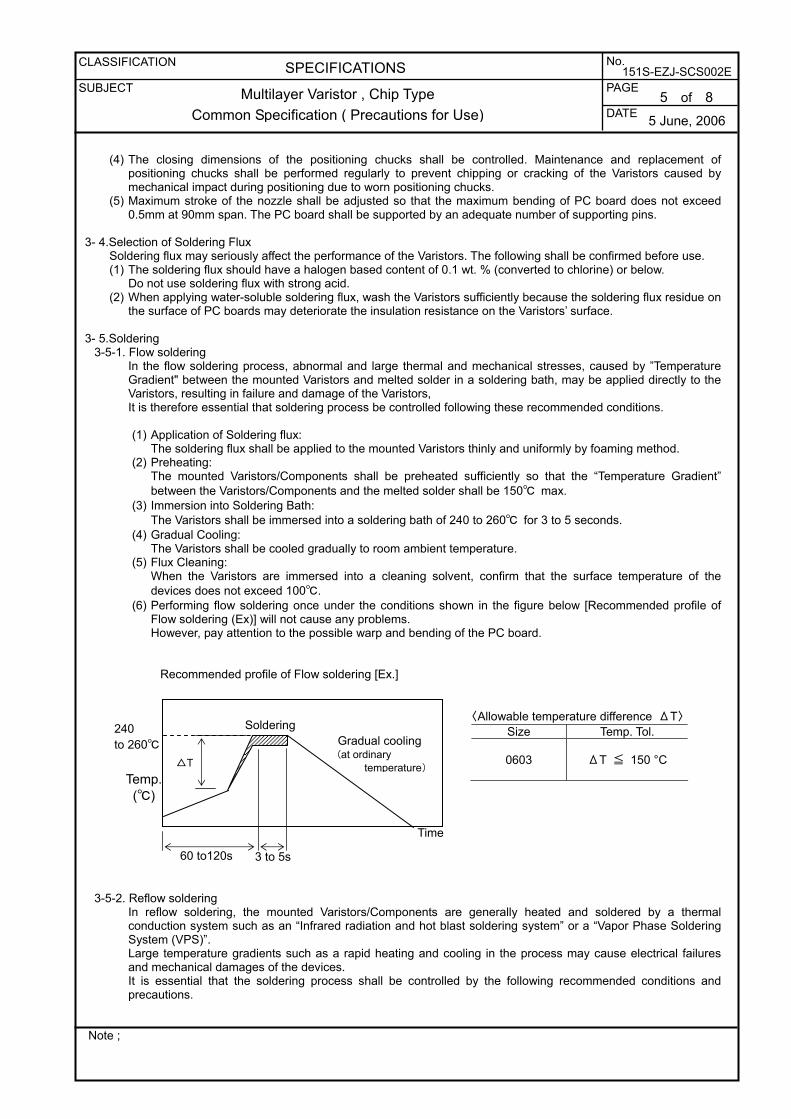
3- 5.Soldering 3-5-1. Flow soldering
In the flow soldering process, abnormal and large thermal and mechanical stresses, caused by ”Temperature Gradient" between the mounted Varistors and melted solder in a soldering bath, may be applied directly to the Varistors, resulting in failure and damage of the Varistors, It is therefore essential that soldering process be controlled following these recommended conditions. (1) Application of Soldering flux:
The soldering flux shall be applied to the mounted Varistors thinly and uniformly by foaming method. (2) Preheating:
The mounted Varistors/Components shall be preheated sufficiently so that the “Temperature Gradient” between the Varistors/Components and the melted solder shall be 150℃ max.
(3) Immersion into Soldering Bath: The Varistors shall be immersed into a soldering bath of 240 to 260℃ for 3 to 5 seconds.
(4) Gradual Cooling: The Varistors shall be cooled gradually to room ambient temperature.
(5) Flux Cleaning: When the Varistors are immersed into a cleaning solvent, confirm that the surface temperature of the devices does not exceed 100℃.
(6) Performing flow soldering once under the conditions shown in the figure below [Recommended profile of Flow soldering (Ex)] will not cause any problems. However, pay attention to the possible warp and bending of the PC board.
Recommended profile of Flow soldering [Ex.]
〈Allowable temperature difference ΔT〉 Size Temp. Tol.
0603
ΔT ≦ 150 °C
3-5-2. Reflow soldering In reflow soldering, the mounted Varistors/Components are generally heated and soldered by a thermal conduction system such as an “Infrared radiation and hot blast soldering system” or a “Vapor Phase Soldering System (VPS)”. Large temperature gradients such as a rapid heating and cooling in the process may cause electrical failures and mechanical damages of the devices. It is essential that the soldering process shall be controlled by the following recommended conditions and precautions.
60 to120s 3 to 5s
Soldering Gradual cooling(at ordinary temperature)△T
240 to 260℃
Time
Temp. (℃)

6 of 8
5 June, 2006
CLASSIFICATION No.
SUBJECT PAGE
DATE
151S-EZJ-SCS002E
Multilayer Varistor , Chip Type Common Specification ( Precautions for Use)
SPECIFICATIONS
Note ;
Temperature Period or Speed ①Preheating 140 to 180 ℃ 60 to 120 s ②Temp. rise Preheating temp. to Peak temp. 2 to 5 ℃/s ③Heating 220 ℃max. 60 s max. ④Peak 260 ℃max. 10 s max. ⑤Gradual cooling Peak temp. to 140 ℃ 1 to 4 ℃/s
When the Varistors are immersed into a cleaning solvent, confirm that the surface temperature of the devices does not exceed 100℃. Performing reflow soldering twice under the conditions shown in the figure above [Recommended profile of Reflow soldering (EX)] will not cause any problems. However, pay attention to the possible warp and bending of the PC board.
Recommended profile of Reflow soldering (Ex.)
〈 Allowable temperature difference ∆T〉
Size Temp. Tol. 0402 to 0805
0504 ∆T≦ 150 °C
3-5-3. Hand soldering When hand soldering Varistors, a large temperature gradient between the preheated Varistors and the tip of the soldering iron may cause electrical failure and mechanical damage such as cracking or breaking of the devices. Soldering shall be carefully controlled and performed such that the temperature gradient is kept at a minimum with the following recommended conditions:
(1) Condition 1 (with preheating)
(a) Soldering : φ1.0mm Thread eutectic solder with soldering flux* in the core. *Rosin-based and non-activated flux is recommended.
(b) Preheating: The Varistors shall be preheated so that “Temperature Gradient” between the devices and the tip of soldering iron is 150℃ or below.
(c) Temperature of Iron tip: 300℃ max. (The required amount of solder shall be melted in advance on the soldering tip.)
(d) Gradual Cooling: After soldering, the Varistors shall be cooled gradually at room ambient temperature.
Recommended profile of Hand Soldering [Ex.]
〈Allowable temperature difference ΔT〉
Size Temp. Tol.
0402 to 0805 ΔT≦ 150 °C
60 to 120 s
Soldering
Gradual cooling
Preheating
3 s max.
△T
Tem
pera
ture
(℃)
Time60 to 120 s 60 s max.
220
260
ΔT
180
140
①Preheating
②Temp. rise
③Heating
⑤Gradual cooling
④Peak
7 of 8
5 June, 2006
CLASSIFICATION No.
SUBJECT PAGE
DATE
151S-EZJ-SCS002E
Multilayer Varistor , Chip Type Common Specification ( Precautions for Use)
SPECIFICATIONS
Note ;
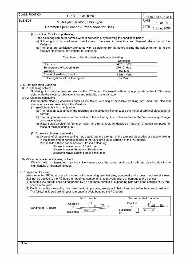
(2) Condition 2 (without preheating) Hand soldering can be performed without preheating, by following the conditions below: (a) Soldering iron tip shall never directly touch the ceramic dielectrics and terminal electrodes of the
Varistors. (b) The lands are sufficiently preheated with a soldering iron tip before sliding the soldering iron tip to the
terminal electrode of the Varistor for soldering. Conditions of Hand soldering without preheating
Condition Chip size 0402 to 0805 Temperature of soldering iron 270 °C Max. Wattage 20W Max. Shape of soldering iron tip φ3mm Max. Soldering time with soldering iron 3s Max.
3- 6.Post Soldering Cleaning
3-6-1. Cleaning solvent Soldering flux residue may remain on the PC board if cleaned with an inappropriate solvent. This may deteriorate the electrical characteristics and reliability of the Varistors.
3-6-2. Cleaning conditions Inappropriate cleaning conditions such as insufficient cleaning or excessive cleaning may impair the electrical characteristics and reliability of the Varistors. (1) Insufficient cleaning can lead to:
(a) The halogen substance in the residues of the soldering flux to cause the metal of terminal electrodes to corrode.
(b) The halogen substance in the residue of the soldering flux on the surface of the Varistors may change resistance values.
(c) Water-soluble soldering flux may have more remarkable tendencies of (a) and (b) above compared to those of rosin soldering flux.
(2) Excessive cleaning can lead to:
(a) Overuse of ultrasonic cleaning may deteriorate the strength of the terminal electrodes or cause cracking in the solder and/or ceramic bodies of the Varistors due to vibration of the PC boards. Please follow these conditions for Ultrasonic cleaning:
Ultrasonic wave output: 20 W/L max. Ultrasonic wave frequency: 40 kHz max. Ultrasonic wave cleaning time: 5 min. max.
3-6-3. Contamination of Cleaning solvent Cleaning with contaminated cleaning solvent may cause the same results as insufficient cleaning due to the high density of liberated halogen.
3- 7.Inspection Process
When mounted PC boards are inspected with measuring terminal pins, abnormal and excess mechanical stress shall not be applied to the PC board or mounted components, to prevent failure or damage to the devices. (1) Mounted PC boards shall be supported by an adequate number of supporting pins with bend settings of 90 mm
span 0.5mm max. (2) Confirm that the measuring pins have the right tip shape, are equal in height and are set in the correct positions.
The following figures are for your reference to avoid bending the PC board. NG Example Recommended Example
Bending of PC board
Separated
Check pin
Supporting pin
Check pin

8 of 8
5 June, 2006
CLASSIFICATION No.
SUBJECT PAGE
DATE
151S-EZJ-SCS002E
Multilayer Varistor , Chip Type Common Specification ( Precautions for Use)
SPECIFICATIONS
Note ;
3- 8.Protective Coating When the surface of a PC board on which the Varistors have been mounted is coated with resin to protect against moisture and dust, make sure that there is no quality deterioration of the Varistors due to protective coating application in actual settings. (1) Do not use coating materials which produce pyrolysis or reaction gas affecting varistor components (2) In resin curing, big stress is applied on varistors by thermal expansion or contraction of resin, which may cause
cracks
3- 9.Dividing/Breaking of PC Boards (1) Abnormal and excessive mechanical stress such as bending or torsion
shown below can cause cracking in the Varistors.
(2) Dividing/Breaking of the PC boards shall be done carefully at moderate speed by using a jig or apparatus to prevent the Varistors on the boards from mechanical damage.
(3) Examples of PCB dividing/breaking jig
The outline of PC board breaking jig is shown below. It is recommended when dividing or breaking PC boards that they are held near the jig where no bending will occur, this way there will be no compressive stress applied to the components or Varistors on the PC board. Do not hold the PC board at a position which is far away from the jig, tensile stress to the Varistors may cause them to crack.
3- 10.Mechanical Impact (1) The Varistors shall be free from any excessive mechanical impact.
The Varistor body is made of ceramics and may be damaged or cracked if dropped. Never use a Varistor which has been dropped; their quality may be impaired and failure rate increased.
(2) When handling PC boards with Varistors mounted on them, do not allow
the Varistors to collide with another PC board. When mounted PC boards are handled or stored in a stacked state, impact between the corner of a PC board and the Varistor may cause damage or cracking and can deteriorate the withstand voltage and insulation resistance of the Varistor.
4. Other
The various precautions described above are typical. For special mounting conditions, please contact us.
Bending
Torsion
PC board splitting jig
V-groove PC board
Outline of Jig
Floor
Crack
Mounted PCB Crack
Recommended dividing
V-groove PC board
Load position
Load direction
NG dividing
Chip component
Load position
PC board
V-groove
Load direction
1 of 5
5 June, 2006
DESIGN
Y.Sasaki
CLASSFICATION No.
SUBJECT PAGE
DATE
151S-EZJ-SCV002E
Multilayer Varistor, Chip Type Taped and Reeled Packaging Specifications
SPECIFICATIONS
APPROVAL
Y.Sakaguti
CHECK T.Kawamura
Note ;
Panasonic Electronic Devices Co., Ltd.
1. Scope This specification applies to taped and reeled packing for Multilayer varistors,chip type.
2. Applicable Standards EIAJ (Electric Industries Association of Japan) Standard EIAJ RC-1009B JIS (Japanese Industrial Standard) Standard JIS C 0806
3. Packing Specification 3- 1.Structure and Dimensions
Paper taping packaging is carried out according the following diagram 1) Carrier tape : Shown in Fig. 5. 2) Reel : Shown in Fig. 6. 3) Packaging : We shall pack suitably in order prevent damage during transportation or storage.
3- 2.Packing Quantity
Carrier-Tape Quantity (pcs./reel)
φ180mm Reel Size (EIA)
Thickness of Capacitor(mm) Material Taping
Pitch PackagingCode Quantity
0402 0.50 +/- 0.05 Paper Taping 2 mm V 10,000 0603 0.8 +/- 0.1 Paper Taping 4 mm V 4,000
0.8 +/- 0.2 Paper Taping 4 mm V 5,000 Y 2,000 0805
1.25 +/- 0.20 Embossed Tap. 4 mmF 3,000
Explanation of Part Numbers (Example) EZJZ 1 V 270 G A
Packaging Code
3- 3.Marking on the Reel The following items are described in the side of a reel in English at least.
1) Part Number 2) Quantity 3) Lot Number 4) Place of origin
2 of 5
5 June, 2006
CLASSFICATION No.
SUBJECT PAGE
DATE
151S-EZJ-SCV002E
Multilayer Varistor, Chip Type Taped and Reeled Packaging Specifications
SPECIFICATIONS
Note ;
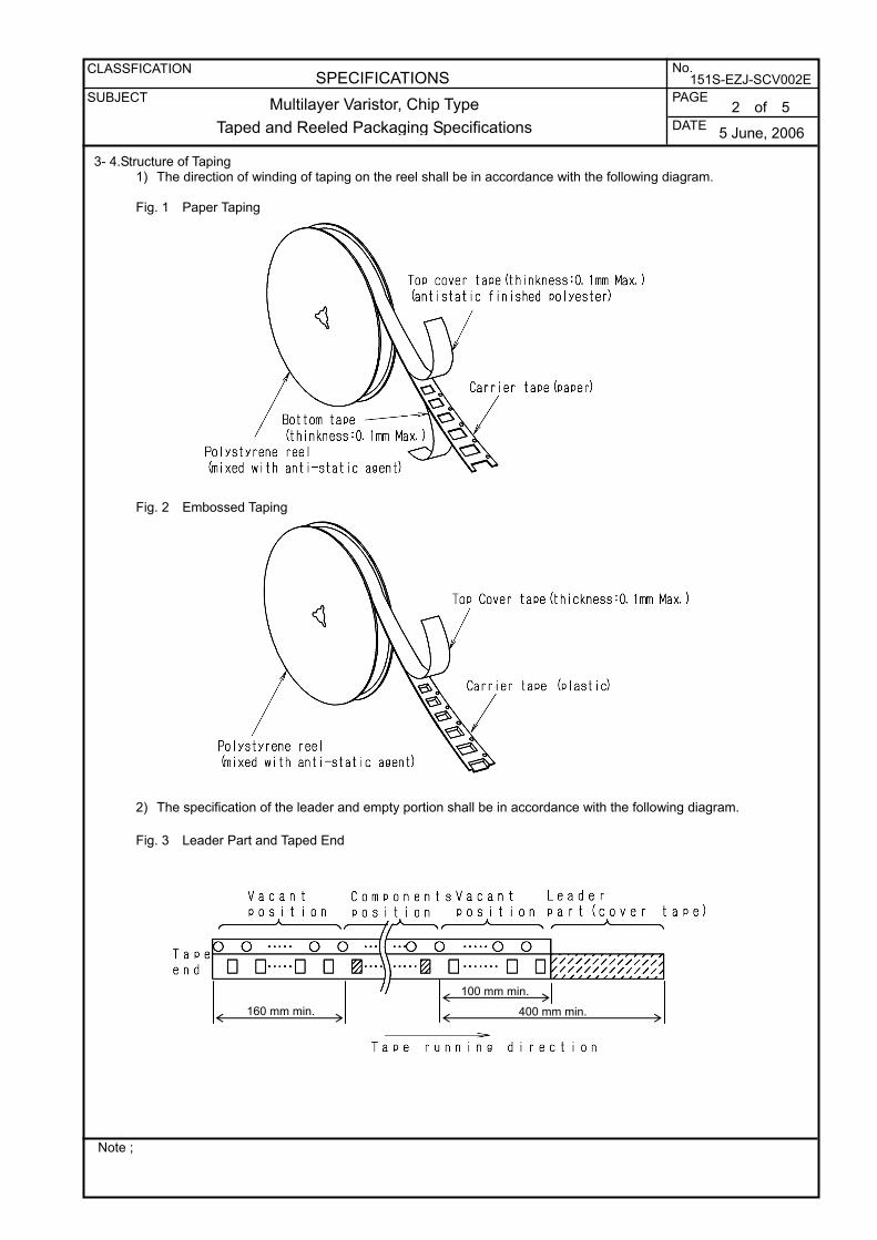
3- 4.Structure of Taping 1) The direction of winding of taping on the reel shall be in accordance with the following diagram.
Fig. 1 Paper Taping
Fig. 2 Embossed Taping
2) The specification of the leader and empty portion shall be in accordance with the following diagram.
Fig. 3 Leader Part and Taped End
160 mm min.
100 mm min.
400 mm min.
3 of 5
5 June, 2006
CLASSFICATION No.
SUBJECT PAGE
DATE
151S-EZJ-SCV002E
Multilayer Varistor, Chip Type Taped and Reeled Packaging Specifications
SPECIFICATIONS
Note ;
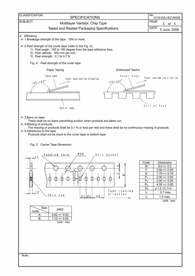
4. Efficiency 4- 1.Breakage strength of the tape : 10N or more.
4- 2.Peel strength of the cover tape (refer to the Fig. 4).
1) Peel angle : 165 to 180 degree from the tape adhesive face. 2) Peel velocity : 300 mm per min. 3) Peel strength : 0.1 to 0.7 N
Fig. 4 Peel strength of the cover tape
Paper Taping Embossed Taping
4- 3.Barrs on tape There shall be no barrs preventing suction when products are taken out.
4- 4.Missing of products The missing of products shall be 0.1 % or less per reel and there shall be no continuous missing of products.
4- 5.Adherence to the tape Products shall not be stuck to the cover tape or bottom tape.
Fig. 5 Carrier Tape Dimension
(a) 0402 Size : 2 mm taping pitch for Paper taping
Code Dimension W 8.0 +/- 0.2 F 3.50 +/- 0.05 E 1.75 +/- 0.10 P1 2.00 +/- 0.05 P2 2.00 +/- 0.05 P0 4.00 +/- 0.05 D0 φ 1.5 +0.1/-0 t1 0.7 max. t2 1.0 max.
Unit : mm
Size Code 0402
A 0.62 +/- 0.05 B 1.12 +/- 0.05
Unit : mm
4 of 5
5 June, 2006
CLASSFICATION No.
SUBJECT PAGE
DATE
151S-EZJ-SCV002E
Multilayer Varistor, Chip Type Taped and Reeled Packaging Specifications
SPECIFICATIONS
Note ;
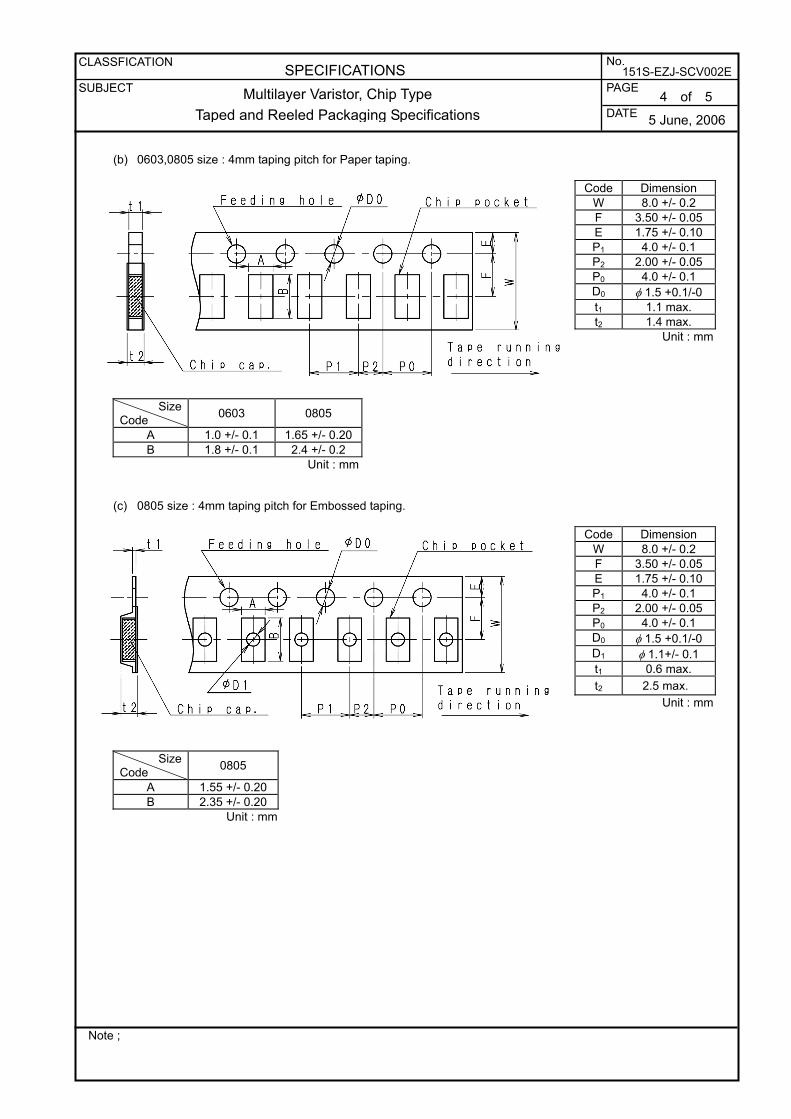
(b) 0603,0805 size : 4mm taping pitch for Paper taping.
Code Dimension
W 8.0 +/- 0.2 F 3.50 +/- 0.05 E 1.75 +/- 0.10 P1 4.0 +/- 0.1 P2 2.00 +/- 0.05 P0 4.0 +/- 0.1 D0 φ 1.5 +0.1/-0 t1 1.1 max. t2 1.4 max.
Unit : mm
Size Code 0603 0805
A 1.0 +/- 0.1 1.65 +/- 0.20B 1.8 +/- 0.1 2.4 +/- 0.2
Unit : mm
(c) 0805 size : 4mm taping pitch for Embossed taping.
Code Dimension W 8.0 +/- 0.2 F 3.50 +/- 0.05 E 1.75 +/- 0.10 P1 4.0 +/- 0.1 P2 2.00 +/- 0.05 P0 4.0 +/- 0.1 D0 φ 1.5 +0.1/-0 D1 φ 1.1+/- 0.1 t1 0.6 max. t2 2.5 max.
Unit : mm
Size Code 0805
A 1.55 +/- 0.20 B 2.35 +/- 0.20
Unit : mm
5 of 5
5 June, 2006
CLASSFICATION No.
SUBJECT PAGE
DATE
151S-EZJ-SCV002E
Multilayer Varistor, Chip Type Taped and Reeled Packaging Specifications
SPECIFICATIONS
Note ;
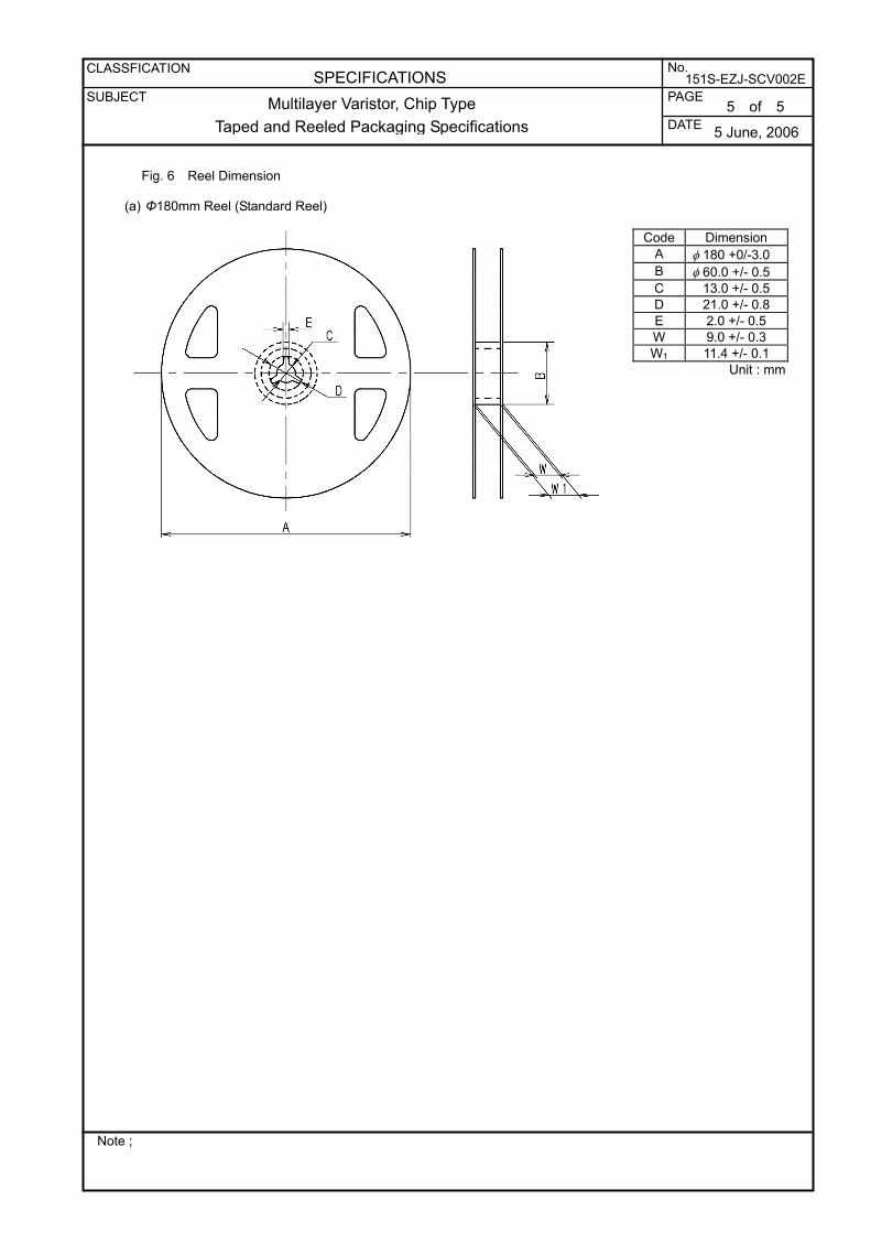
Fig. 6 Reel Dimension
(a) Φ180mm Reel (Standard Reel)
Code Dimension
A φ 180 +0/-3.0 B φ 60.0 +/- 0.5 C 13.0 +/- 0.5 D 21.0 +/- 0.8 E 2.0 +/- 0.5 W 9.0 +/- 0.3 W1 11.4 +/- 0.1
Unit : mm