Embed Size (px)
Citation preview

Prof. John NestorECE DepartmentLafayette College
Easton, Pennsylvania 18042
ECE 313 - Computer Organization
Lecture 15 - Multi-Cycle Processor Design 2Fall 2004
Reading: 5.6 - 5.11, C.4 - C.5, Verilog Handout Section 6-10
HW Due Fri. 11/19: 5.32, 5.34, 5.35, 5.47, 5.49, 5.55
Portions of these slides are derived from: Textbook figures © 1998 Morgan Kaufmann Publishers all rights reserved Tod Amon's COD2e Slides © 1998 Morgan Kaufmann Publishers all rights reserved Dave Patterson’s CS 152 Slides - Fall 1997 © UCB Rob Rutenbar’s 18-347 Slides - Fall 1999 CMU other sources as noted

ECE 313 Fall 2004 Lecture 15 - Multicycle Design 2 2
Outline - Multicycle Design
Overview Datapath Design Controller Design Aside: FSM Design in Verilog Performance Considerations Extending the Design: An Example Microprogramming Exceptions

ECE 313 Fall 2004 Lecture 15 - Multicycle Design 2 3
Review State Machine Design
Traditional Approach: Create State Diagram Create State Transition Table Assign State Codes Write Excitation Equations & Minimize
HDL-Based State Machine Design Create State Diagram (optional) Write HDL description of state machine Synthesize

ECE 313 Fall 2004 Lecture 15 - Multicycle Design 2 4
Review - State Transition Table / Diagram
Transition List - lists edges in STDPS Condition NS Output
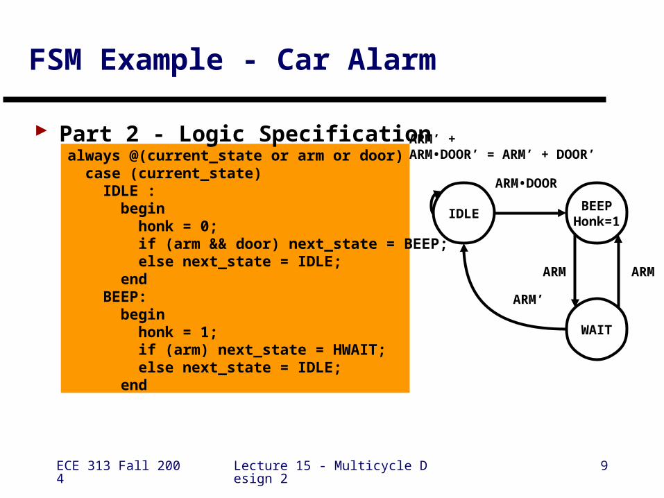
IDLE ARM' + DOOR' IDLE 0
IDLE ARM*DOOR BEEP 0
BEEP ARM WAIT 1
BEEP ARM' IDLE 1
WAIT ARM BEEP 0
WAIT ARM' IDLE 0
IDLEBEEP
Honk=1
WAIT
ARM•DOOR
ARMARM
ARM’
ARM’ + ARM•DOOR’= ARM’ + DOOR’

ECE 313 Fall 2004 Lecture 15 - Multicycle Design 2 5
Coding FSMs in Verilog
Clocked always block - state register Combinational always block -
next state logic output logic
Next-StateLogic
D Q
D Q
OutputLogic
clock

ECE 313 Fall 2004 Lecture 15 - Multicycle Design 2 6
Coding FSMs in Verilog - Code Skeleton
Part 1 - Declarationsmodule fsm(inputs, outputs); input . . .; input . . .; reg . . .;
parameter [NBITS-1:0]S0 = 2'b00;S1 = 2'b01;S2 = 2b'10;S3 = 2b'11;
reg [NBITS-1 :0] CURRENT_STATE; reg [NBITS-1 :0] NEXT_STATE;
State Codes
State Variable

ECE 313 Fall 2004 Lecture 15 - Multicycle Design 2 7
Coding FSMs in Verilog - Code Skeleton
Part 2 - State Register, Logic Specification always @(posedge clk) begin CURRENT_STATE <= NEXT_STATE; end
always @(CURRENT_STATE or xin) begin case (CURRENT_STATE) S0: . . . determine NEXT_STATE, outputs
S1 : . . . determine NEXT_STATE, outputs end case end // alwaysendmodule

ECE 313 Fall 2004 Lecture 15 - Multicycle Design 2 8
FSM Example - Car Alarm
Part 1 - Declarations, State Registermodule car_alarm (arm, door, reset, clk, honk ); input arm, door, reset, clk; output honk; reg honk;
parameter IDLE=0,BEEP=1,HWAIT=2; reg [1:0] current_state, next_state;
always @(posedge reset or posedge clk) if (reset) current_state <= IDLE; else current_state <= next_state;
ECE 313 Fall 2004 Lecture 15 - Multicycle Design 2 9
FSM Example - Car Alarm
Part 2 - Logic Specificationalways @(current_state or arm or door) case (current_state) IDLE : begin honk = 0; if (arm && door) next_state = BEEP; else next_state = IDLE; end BEEP: begin honk = 1; if (arm) next_state = HWAIT; else next_state = IDLE; end
IDLEBEEP
Honk=1
WAIT
ARM•DOOR
ARMARM
ARM’
ARM’ + ARM•DOOR’ = ARM’ + DOOR’

ECE 313 Fall 2004 Lecture 15 - Multicycle Design 2 10
FSM Example - Car Alarm
Part 3 - Logic Specification (cont’d)
HWAIT : begin honk = 0; if (arm) next_state = BEEP; else next_state = IDLE; end default : begin honk = 0; next_state = IDLE; end endcaseendmodule
IDLEBEEP
Honk=1
WAIT
ARM•DOOR
ARMARM
ARM’
ARM’ + ARM•DOOR’ = ARM’ + DOOR’

ECE 313 Fall 2004 Lecture 15 - Multicycle Design 2 11
FSM Example - Verilog Handout
Divide-by-Three Counter
S0out=0
S1out=0
S1out=1
reset

ECE 313 Fall 2004 Lecture 15 - Multicycle Design 2 12
Verilog Code - Divide by Three CounterPart 1
module divideby3FSM(clk, reset, out);input clk;input reset;output out;
reg [1:0] state;reg [1:0] nextstate;
parameter S0 = 2’b00;parameter S1 = 2’b01;parameter S2 = 2’b10;
// State Register
always @(posedge clk or posedge reset)if (reset) state <= S0;else state <= nextstate;

ECE 313 Fall 2004 Lecture 15 - Multicycle Design 2 13
Verilog Code - Divide by Three CounterPart 2
// Next State Logic
always @(state)case (state)
S0: nextstate = S1;S1: nextstate = S2;S2: nextstate = S0;default: nextstate = S0;
endcase
// Output Logic
assign out = (state == S2);endmodule

ECE 313 Fall 2004 Lecture 15 - Multicycle Design 2 14
Verilog Example: MIPS Control Unit
0 Instruction FetchInstruction decode /
register fetch
1
2
Memory addresscomputation
3
4
5 7
6 8 9Execution
BranchCompletion
JumpCompletion
Memoryaccess
Memoryaccess
R-type completion
Writeback step
Start
MemReadALUSrcA = 0
IorD = 0IRWrite
ALUSrcB = 01ALUOp = 00
PCWritePCSource = 00
(OP = ‘JMP’)
ALUSrcA = 0ALUSrcB = 11ALUOp = 00
ALUSrcA = 1ALUSrcB = 10ALUOp = 00
(OP = ‘LW’)
(OP = (‘SW’)
MemReadIorD = 1
RegWriteMemToReg=1
RegDst = 0
MemWriteIorD = 1
ALUSrcA = 1ALUSrcB = 00ALUOp = 10
RegDst = 1RegWrite
MemtoReg = 0
ALUSrcA = 1ALUSrcB = 00ALUOp = 01
PCWriteCondPCSource = 01
PCWritePCSource = 10

ECE 313 Fall 2004 Lecture 15 - Multicycle Design 2 15
Review: Full Multicycle Implementation
ALUControl
ControlUnit
6 6op I[31:26] funct I[5:0]
ALUOp
2
5 5
RD1
RD2
RN1 RN2 WN
WD
RegWrite
Registers
Operation
ALU
3
EXTND
16 32
ZeroRD
WDMemRead
MemoryADDR
MemWrite
5
Instruction I
32
ALUSrcB
<<2
PC
4
RegDst
5
IR
MDR
MUX
0123
MUX
1
0
MUX
0
1A
BALUOUT
0
1
2MUX
<<2 CONCAT28 32
MUX
0
1
ALUSrcA
jmpaddrI[25:0]
rd
MUX0 1
rtrs
immediate
PCSource
MemtoReg
IorD
PCWriteCond
PCWrite
Zero
IRWrite

ECE 313 Fall 2004 Lecture 15 - Multicycle Design 2 16
MIPS Control Unit “Skeleton” - Part 1
module mips_control( clk, reset, Op, PCWrite, PCWriteCond, IorD, MemRead, MemWrite, MemtoReg, IRWrite, PCSource, ALUOp ALUSrcB, ALUSrcA, RegWrite, RegDst );input clk;input reset;input [5:0] Op;output PCWrite;output PCWriteCond;output IorD;output MemRead;output MemWrite;output MemtoReg;output IRWrite;output [1:0] PCSource;output [1:0] ALUOp;output ALUSrcA;output [1:0] ALUSrcB;output RegWrite;output RegDst;
port declarations

ECE 313 Fall 2004 Lecture 15 - Multicycle Design 2 17
MIPS Control Unit “Skeleton” - Part 2
reg PCWrite;reg PCWriteCond;reg IorD;reg MemRead;reg MemWrite;reg MemtoReg;reg IRWrite;reg [1:0] PCSource;reg [1:0] ALUOp;reg ALUSrcA;reg [1:0] ALUSrcB;reg RegWrite;reg RegDst;
parameter R_FORMAT = 6'd0;parameter LW = 6'd35;parameter SW = 6'd43;parameter BEQ = 6'd4;parameter J = 6’d2;
parameter S0=4'd0, S1=4'd1, S2=4'd2, S3=4'd3, S4=4'd4, S5=4'd5, S6=4'd6, S7=4'D7, S8=4'd8, S9=4'd9;
Symbolic Constants - opcodes
Symbolic Constants - state codes
reg declarations for output ports

ECE 313 Fall 2004 Lecture 15 - Multicycle Design 2 18
MIPS Control Unit “Skeleton” - Part 3
reg [3:0] current_state, next_state;
always @(negedge clk) begin if (reset) current_state <= S0; else current_state <= next_state;end
always @(current_state or Op)
begin
// default values
PCWrite = 1'b0;
PCWriteCond = 1'b0;
IorD = 1'bx;
MemRead = 1'b0;
MemWrite = 1'b0;
MemtoReg = 1'bx;
IRWrite = 1'b0;
PCSource = 2'bxx;
ALUOp = 2'bxx;
ALUSrcA = 1'bx;
ALUSrcB = 2'bxx;
RegWrite = 1'b0;
RegDst = 1'bx;
case (current_state)
S0: begin
MemRead = 1'b1;
ALUSrcA = 1'b0;
IorD = 1'b0;
IRWrite = 1'b1;
ALUSrcB = 2'b01;
ALUOp = 2'b00;
PCWrite = 1'b1;
PCSource = 2'b00;
next_state = S1;
end
…
endcase
end
endmodule
Add code here!DefaultValues
More DefaultValues

ECE 313 Fall 2004 Lecture 15 - Multicycle Design 2 19
Controller Implementation
Typical Implementation: Figure 5-37, p. 338 Variations
Random logic PLA ROM
• address lines = inputs
• data lines = outputs
• contents = “truth table”
Datapathcontroloutputs
Inputs fromInstr. Reg(opcode)
CombinationalControlLogic
State
NextState

ECE 313 Fall 2004 Lecture 15 - Multicycle Design 2 20
Outline - Multicycle Design
Overview Datapath Design Controller Design Aside: FSM Design in Verilog Performance Considerations Extending the Design: An Example Microprogramming Exceptions

ECE 313 Fall 2004 Lecture 15 - Multicycle Design 2 21
Performance of a Multicycle Implementation
What is the CPI of the Multicycle Implementation? Using measured instruction mix from SPECINT2000
lw 5 cycles 25%sw 4 cycles 10%R-type 4 cycles 52%branch 3 cycles 11%jump 3 cycles 2%
What is the CPI? CPI = (5 cycles * 0.25) + (4 cycles * 0.10) + (4 cycles * 0.53)
+ (3 cycles * 0.11) + (3 cycles * 0.02) CPI = 4.12 cycles per instruction

ECE 313 Fall 2004 Lecture 15 - Multicycle Design 2 22
Performance Continued
Assuming a 200ps clock, what is average execution time/instruction? Sec/Instr = 4.12 CPI * 200ps/cycle) = 824ps/instr
How does this compare to the Single-Cycle Case? Sec/Instr = 1 CPI * 600ps/cycle = 600ps/instr Single-Cycle is 1.38 times faster than Multicycle
Why is Single-Cycle faster than Multicycle? Branch & jump are the same speed (600ps vs 600ps) R-type & store are faster (600ps vs 800ps) Load word is faster (600ps vs 1000ps)

ECE 313 Fall 2004 Lecture 15 - Multicycle Design 2 23
Outline - Multicycle Design
Overview Datapath Design Controller Design Aside: FSM Design in Verilog Performance Considerations Extending the Design: An Example Microprogramming Exceptions

ECE 313 Fall 2004 Lecture 15 - Multicycle Design 2 24
Multicycle Example Problem
Extend the design to implement the “jr” (jump register) instruction:
jr rs PC = Reg[rs]
Format:
Steps:1. Review instruction requirements (register transfer)
2. Modify datapath
3. Modify control logic
0 rs 0 0 80
6 bits 5 bits 5 bits 5 bits 5 bits 6 bits

ECE 313 Fall 2004 Lecture 15 - Multicycle Design 2 25
Reg[rs]
Example Problem: Datapath
What needs to be changed?
ALUControl
ControlUnit
6 6op I[31:26] funct I[5:0]
ALUOp
2
5 5
RD1
RD2
RN1 RN2 WN
WD
RegWrite
Registers
Operation
ALU
3
EXTND
16 32
ZeroRD
WDMemRead
MemoryADDR
MemWrite
5
Instruction I
32
ALUSrcB
<<2
PC
4
RegDst
5
IR
MDR
MUX
0123
MUX
1
0
MUX
0
1A
BALUOUT
0
1
2MUX
<<2 CONCAT28 32
MUX
0
1
ALUSrcA
jmpaddrI[25:0]
rd
MUX0 1
rtrs
immediate
PCSource
MemtoReg
IorD
PCWriteCond
PCWrite
Zero
IRWrite
32
1
0

ECE 313 Fall 2004 Lecture 15 - Multicycle Design 2 26
Example Problem: Control
What needs to be changed?
PCWritePCSource = 11
(OP = ‘JR‘)
0 Instruction FetchInstruction decode /
register fetch
1
2
Memory addresscomputation
3
4
5 7
6 8 9Execution
BranchCompletion
JumpCompletion
Memoryaccess
Memoryaccess
R-type completion
Writeback step
Start
MemReadALUSrcA = 0
IorD = 0IRWrite
ALUSrcB = 01ALUOp = 00
PCWritePCSource = 00
(OP = ‘JMP’)
ALUSrcA = 0ALUSrcB = 11ALUOp = 00
ALUSrcA = 1ALUSrcB = 10ALUOp = 00
(OP = ‘LW’)
(OP = (‘SW’)
MemReadIorD = 1
RegWriteMemToReg=1
RegDst = 0
MemWriteIorD = 1
ALUSrcA = 1ALUSrcB = 00ALUOp = 10
RegDst = 1RegWrite
MemtoReg = 0
ALUSrcA = 1ALUSrcB = 00ALUOp = 01
PCWriteCondPCSource = 01
PCWritePCSource = 10

ECE 313 Fall 2004 Lecture 15 - Multicycle Design 2 27
Outline - Multicycle Design
Overview Datapath Design Controller Design Aside: FSM Design in Verilog Performance Considerations Extending the Design: An Example Microprogramming Exceptions

ECE 313 Fall 2004 Lecture 15 - Multicycle Design 2 28
Control Implementation - Another View
Separate Logic into two pieces Output Logic (this is a Moore Machine - why?) Next-State Logic
Datapath ControlOutputsOutput
Logic
n
State
nNext-State Logic
Inputs from IR(Opcode)
n

ECE 313 Fall 2004 Lecture 15 - Multicycle Design 2 29
Microprogramming - Motivation
Problems with graphical approach to FSM Design Unwieldy for large number of states (real processors may
have hundreds of instructions -> hundreds of states) Unwieldy if instruction types vary radically
(can you say… x86?) Most states are sequential (state 4 follows state 3; state 3
follows state 2; state 7 follows state 6; etc.
Idea: expand on ROM implementation of control

ECE 313 Fall 2004 Lecture 15 - Multicycle Design 2 30
Consider Output Logic in ROM
ROM Characteristics - "lookup table" State code for each state is a ROM address Control outputs for each state are a ROM word
Datapath ControlOutputsOutput
Logic
n
State
nNext-State Logic
Inputs from IR(Opcode)
n

ECE 313 Fall 2004 Lecture 15 - Multicycle Design 2 31
Microprogramming - Basic Idea
Idea: expand on ROM control implementation One state = one ROM word = one microinstruction State sequences form a microprogram Each state code becomes a microinstruction address
Datapath ControlOutputsMicrocode
Storage(ROM)
n
MicroprogramCounter
nMicroinstructionaddress
Sequencing Logic
Inputs from IR(Opcode)
n
SequenceControl
Microinstruction

ECE 313 Fall 2004 Lecture 15 - Multicycle Design 2 32
Microprogramming - Sequencer Design
Datapath ControlOutputsMicrocode
Storage(ROM)
n
µPC
Microinstructionaddress
Dispatch ROM 2
Inputs from IR(Opcode)
n
SequenceControl
Microinstruction
+
1
n
n
Dispatch ROM 10
n0
1
2
3

ECE 313 Fall 2004 Lecture 15 - Multicycle Design 2 33
Describing Microcode
Each microinstruction is lots of 1's and 0's To ease understanding:
Break into fields related to different datapath functions Use mnemonics to describe different field values
DatapathControlSignals
ALU control SequencingLabelAdd Read PC ALU SeqstringSubt
Func Code
PCA
B4
Extend
Extshft
ReadWrite ALUWrite MDR
Read ALUWrite ALU
ALUOut-condJump address
FetchDispatch i
See also: Figure C.5.1, p. C-28
SRC1 Reg. control Memory PCWrite control
AL
UO
p
AL
US
rcA
AL
US
rcB
Reg
Wri
te
Reg
Dst
Mem
Rea
dSRC2
Mem
Wri
te
IRW
rite
PC
Wri
te
PC
Wri
teC
on
d
IorD
PC
So
urc
e
Mem
toR
eg
Ad
drC
tl
SequencerControlSignal

ECE 313 Fall 2004 Lecture 15 - Multicycle Design 2 34
Microcode for Multicycle Implementation
LabelALU
control SRC1 SRC2Register control Memory
PCWrite control Sequencing
Fetch Add PC 4 Read PC ALU SeqAdd PC Extshft Read Dispatch 1
Mem1 Add A Extend Dispatch 2LW2 Read ALU Seq
Write MDR FetchSW2 Write ALU Fetch
Rformat1 Func code A B SeqWrite ALU Fetch
BEQ1 Subt A B ALUOut-cond FetchJUMP1 Jump address Fetch

ECE 313 Fall 2004 Lecture 15 - Multicycle Design 2 35
Sequencer Implementation Details
Dispatch ROM 1 Dispatch ROM 2Op Opcode name Value Op Opcode name Value
000000 R-format 0110 100011 lw 0011000010 jmp 1001 101011 sw 0101000100 beq 1000100011 lw 0010101011 sw 0010
Datapath ControlOutputsMicrocode
Storage(ROM)
n
µPC
Dispatch ROM 2
Inputs from IR(Opcode)
n
+
1
n
n
Dispatch ROM 10
n0
1
2
3
AddrCtl

ECE 313 Fall 2004 Lecture 15 - Multicycle Design 2 36
Microcoding Tradeoffs
+ Makes design easier+ Flexible
Easy to adapt to changes in organization, timing, technology
Can make changes late in design cycle Can add more instructions just by adding microcode
- Costly to implement- Slow - "extra level" of interpretation

ECE 313 Fall 2004 Lecture 15 - Multicycle Design 2 37
Microcoding Perspective
Not used in modern RISC processors simple instructions -> simple control hardwired control -> faster execution pipelining used to enhance performance
Used heavily in CISC processors Traditional CISC:
• all instructions microcoded• multiple dispatch ROMs to handle different instruction
classes, addressing modes, etc. Current CISC (see Section 5.9)
• Microinstructions pipelined like RISC instructions!• Simple instructions translate to one microinstruction• Complex instructions translate to multiple microinstructions

ECE 313 Fall 2004 Lecture 15 - Multicycle Design 2 38
Instruction Decoding in the Pentium 4
Source: “The Microarchitecture of the Pentium® 4 Processor”, Intel Technology Journal, First Quarter 2001http://developer.intel.com/technology/itj/q12001/articles/art_2.htm.

ECE 313 Fall 2004 Lecture 15 - Multicycle Design 2 39
Coming Up
Implementing Exceptions Pipelined Design