Embed Size (px)
Citation preview

Si8239x Data Sheet
4.0 A ISODrivers with 2.5 V VDDI and Safety FeaturesThe Si8239x combines two isolated drivers with either an independent input control or asingle input into a single package for high power applications. All drivers operate with a2.5 V input VDD and a maximum drive supply voltage of 24 V.
The Si8239x isolators are ideal for driving power MOSFETs and IGBTs used in a widevariety of switched power and motor control applications. These drivers utilize SiliconLaboratories' proprietary silicon isolation technology, supporting up to 5 kVRMS with-stand voltage. This technology enables high CMTI (100 kV/µs), lower prop delays andskew, reduced variation with temperature and age and tighter part-to-part matching.
It also offers some unique features such as an output UVLO fault detection and feed-back, and automatic shutdown for both drivers, an EN (active high) pin, a safe delayedstart-up time of 1 ms, fail-safe drivers with default low in case of VDDI power-down, anddead time programmability. The Si8239x family offers longer service life and dramaticallyhigher reliability compared to opto-coupled gate drivers.
Automotive Grade is available for certain part numbers. These products are built usingautomotive-specific flows at all steps in the manufacturing process to ensure the robust-ness and low defectivity required for automotive applications.
KEY FEATURES
• Two isolated drivers in one package• Up to 5 kVRMS isolation• Up to 1500 VDC peak driver-to-driver
differential voltage• Enhanced output UVLO safety
• Status feedback to controller• Both outputs drive low on UVLO
• EN pin for enhanced safety• Extended VDDI: 2.5 V – 5.5 V• PWM and dual driver versions• 4.0 A peak output• High electromagnetic immunity• Extended start-up time (1ms) for safe
initialization sequence• 30 ns propagation delay• Transient immunity: 100 kV/µs• Programmable dead time
• 10–200 ns• 40–600 ns
• Deglitch option for filtering noise• Wide operating range
• –40 to +125 °C• RoHS-compliant packages
• SOIC-14/-16 wide body• SOIC-16 narrow body
• AEC-Q100 qualified• Automotive-grade OPNs available
• AIAG compliant PPAP documentationsupport
• IMDS and CAMDS listing support
Industrial Applications• Power Delivery Systems• Motor Control Systems• Isolated DC-DC Power Supplies• Lighting Control Systems• Solar and Industrial Inverters
Safety Approvals (Pending)• UL 1577 recognized
• Up to 5000 Vrms for 1 minute• CSA approval
• IEC60950-1, 62368-1 (reinforced in-sulation)
• VDE certification conformity• VDE 0884-10 (basic insulation)• EN60950-1, 62368-1 (reinforced in-
sulation)• CQC certification approval
• GB4943.1-2011 (reinforced insula-tion)
Automotive Applications• On-board chargers• Battery management systems• Charging stations• Traction inverters• Hybrid Electric Vehicles• Battery Electric Vehicles
Skyworks Solutions, Inc. • Phone [781] 376-3000 • Fax [781] 376-3100 • [email protected] • www.skyworksinc.com1 Rev. 1.02 • Skyworks Proprietary Information • Products and Product Information are Subject to Change Without Notice • July 26, 2021 1

Table of Contents1. Ordering Guide . . . . . . . . . . . . . . . . . . . . . . . . . . . . . . 4
2. System Overview . . . . . . . . . . . . . . . . . . . . . . . . . . . . . . 72.1 Typical Performance Characteristics. . . . . . . . . . . . . . . . . . . . . . . 8
2.2 Family Overview and Logic Operation During Startup . . . . . . . . . . . . . . . . . 92.2.1 Device Behavior . . . . . . . . . . . . . . . . . . . . . . . . . . . .10
2.3 Power Supply Connections . . . . . . . . . . . . . . . . . . . . . . . . . .12
2.4 Power Dissipation Considerations . . . . . . . . . . . . . . . . . . . . . . .13
2.5 Layout Considerations . . . . . . . . . . . . . . . . . . . . . . . . . . .14
2.6 Undervoltage Lockout Operation . . . . . . . . . . . . . . . . . . . . . . . .142.6.1 Device Startup . . . . . . . . . . . . . . . . . . . . . . . . . . . .142.6.2 Undervoltage Lockout . . . . . . . . . . . . . . . . . . . . . . . . . .152.6.3 Control Inputs . . . . . . . . . . . . . . . . . . . . . . . . . . . . .162.6.4 Enable Input . . . . . . . . . . . . . . . . . . . . . . . . . . . . .162.6.5 Delayed Startup Time . . . . . . . . . . . . . . . . . . . . . . . . . .162.6.6 RDY Pin. . . . . . . . . . . . . . . . . . . . . . . . . . . . . . .16
2.7 Overlap Protection and Programmable Dead Time . . . . . . . . . . . . . . . . . .17
2.8 De-glitch Feature . . . . . . . . . . . . . . . . . . . . . . . . . . . . .17
3. Applications. . . . . . . . . . . . . . . . . . . . . . . . . . . . . . . 183.1 High-Side/Low-Side Driver . . . . . . . . . . . . . . . . . . . . . . . . . .18
3.2 Dual Driver . . . . . . . . . . . . . . . . . . . . . . . . . . . . . . .19
3.3 Enhanced UVLO . . . . . . . . . . . . . . . . . . . . . . . . . . . . .19
4. Electrical Characteristics . . . . . . . . . . . . . . . . . . . . . . . . . . 20
5. Top-Level Block Diagrams . . . . . . . . . . . . . . . . . . . . . . . . . 29
6. Pin Descriptions . . . . . . . . . . . . . . . . . . . . . . . . . . . . . 32
7. Package Outline: 14-Pin Wide Body SOIC. . . . . . . . . . . . . . . . . . . . 33
8. Land Pattern: 14-Pin Wide Body SOIC . . . . . . . . . . . . . . . . . . . . . 34
9. Package Outline: 16-Pin Wide Body SOIC. . . . . . . . . . . . . . . . . . . . 35
10. Land Pattern: 16-Pin Wide Body SOIC . . . . . . . . . . . . . . . . . . . . 37
11. Package Outline: 16-Pin Narrow Body SOIC . . . . . . . . . . . . . . . . . . 38
12. Land Pattern: 16-Pin Narrow Body SOIC. . . . . . . . . . . . . . . . . . . . 39
13. Top Markings . . . . . . . . . . . . . . . . . . . . . . . . . . . . . . 4013.1 Si8239x Top Marking (14-/16-Pin Wide Body SOIC) . . . . . . . . . . . . . . . . .40
13.2 Top Marking Explanation (16-Pin Wide Body SOIC) . . . . . . . . . . . . . . . . .40
13.3 Si8239x Top Marking (16-Pin Narrow Body SOIC) . . . . . . . . . . . . . . . . .41
13.4 Top Marking Explanation (16-Pin Narrow Body SOIC) . . . . . . . . . . . . . . . .41
Skyworks Solutions, Inc. • Phone [781] 376-3000 • Fax [781] 376-3100 • [email protected] • www.skyworksinc.com2 Rev. 1.02 • Skyworks Proprietary Information • Products and Product Information are Subject to Change Without Notice • July 26, 2021 2
14. Revision History. . . . . . . . . . . . . . . . . . . . . . . . . . . . . 42
Skyworks Solutions, Inc. • Phone [781] 376-3000 • Fax [781] 376-3100 • [email protected] • www.skyworksinc.com3 Rev. 1.02 • Skyworks Proprietary Information • Products and Product Information are Subject to Change Without Notice • July 26, 2021 3

1. Ordering Guide
Industrial and Automotive Grade OPNs
Industrial-grade devices (part numbers having an “-I” in their suffix) are built using well-controlled, high-quality manufacturing flows toensure robustness and reliability. Qualifications are compliant with JEDEC, and defect reduction methodologies are used throughoutdefinition, design, evaluation, qualification, and mass production steps.
Automotive-grade devices (part numbers having an “-A” in their suffix) are built using automotive-specific flows at all steps in themanufacturing process to ensure robustness and low defectivity. These devices are supported with AIAG-compliant Production PartApproval Process (PPAP) documentation, and feature International Material Data System (IMDS) and China Automotive MaterialData System (CAMDS) listing. Qualifications are compliant with AEC-Q100, and a zero-defect methodology is maintained throughoutdefinition, design, evaluation, qualification, and mass production steps.
Table 1.1. Si8239x Ordering Guide
Ordering PartNumber
(OPN)
Automotive GradeOPN
OutputUVLO
EnhancedUVLO
UVLOStatus
Pin
DelayedStartup
Time
Dead-Time Set-
ting
Deglitch Package Type
Independent dual drivers with separate VIA, VIB inputs
Si82390AB-IS1 Si82390AB-AS1 6 V Yes Yes Yes N/A No SOIC-16 NB
Si82390BB-IS1 Si82390BB-AS1 8 V Yes Yes Yes N/A No SOIC-16 NB
Si82390CB-IS1 Si82390CB-AS1 12 V Yes Yes Yes N/A No SOIC-16 NB
Si82391AB-IS1 Si82391AB-AS1 6 V Yes Yes No N/A No SOIC-16 NB
Si82391BB-IS1 Si82391BB-AS1 8 V Yes Yes No N/A No SOIC-16 NB
Si82391CB-IS1 Si82391CB-AS1 12 V Yes Yes No N/A No SOIC-16 NB
Si82395AB-IS1 Si82395AB-AS1 6 V No Yes Yes N/A No SOIC-16 NB
Si82395BB-IS1 Si82395BB-AS1 8 V No Yes Yes N/A No SOIC-16 NB
Si82395CB-IS1 Si82395CB-AS1 12 V No Yes Yes N/A No SOIC-16 NB
Si82396AB-IS1 Si82396AB-AS1 6 V No Yes No N/A No SOIC-16 NB
Si82396BB-IS1 Si82396BB-AS1 8 V No Yes No N/A No SOIC-16 NB
Si82396CB-IS1 Si82396CB-AS1 12 V No Yes No N/A No SOIC-16 NB
Si82390AD-IS Si82390AD-AS 6 V Yes Yes Yes N/A No SOIC-16 WB
Si82390BD-IS Si82390BD-AS 8 V Yes Yes Yes N/A No SOIC-16 WB
Si82390CD-IS Si82390CD-AS 12 V Yes Yes Yes N/A No SOIC-16 WB
Si82391AD-IS Si82391AD-AS 6 V Yes Yes No N/A No SOIC-16 WB
Si82391BD-IS Si82391BD-AS 8 V Yes Yes No N/A No SOIC-16 WB
Si82391CD-IS Si82391CD-AS 12 V Yes Yes No N/A No SOIC-16 WB
Si82395AD-IS Si82395AD-AS 6 V No Yes Yes N/A No SOIC-16 WB
Si82395BD-IS Si82395BD-AS 8 V No Yes Yes N/A No SOIC-16 WB
Si82395CD-IS Si82395CD-AS 12 V No Yes Yes N/A No SOIC-16 WB
Si82396AD-IS Si82396AD-AS 6 V No Yes No N/A No SOIC-16 WB
Si82396BD-IS Si82396BD-AS 8 V No Yes No N/A No SOIC-16 WB
Si82396CD-IS Si82396CD-AS 12 V No Yes No N/A No SOIC-16 WB
Si8239x Data Sheet • Ordering Guide
Skyworks Solutions, Inc. • Phone [781] 376-3000 • Fax [781] 376-3100 • [email protected] • www.skyworksinc.com4 Rev. 1.02 • Skyworks Proprietary Information • Products and Product Information are Subject to Change Without Notice • July 26, 2021 4

Ordering PartNumber
(OPN)
Automotive GradeOPN
OutputUVLO
EnhancedUVLO
UVLOStatus
Pin
DelayedStartup
Time
Dead-Time Set-
ting
Deglitch Package Type
Si82397AD-IS Si82397AD-AS 6 V No No Yes N/A No SOIC-16 WB
Si82397BD-IS Si82397BD-AS 8 V No No Yes N/A No SOIC-16 WB
Si82397CD-IS Si82397CD-AS 12 V No No Yes N/A No SOIC-16 WB
Si82390AD-IS3 Si82390AD-AS3 6 V Yes Yes Yes N/A No SOIC-14 WB
Si82390BD-IS3 Si82390BD-AS3 8 V Yes Yes Yes N/A No SOIC-14 WB
Si82390CD-IS3 Si82390CD-AS3 12 V Yes Yes Yes N/A No SOIC-14 WB
Si82391AD-IS3 Si82391AD-AS3 6 V Yes Yes No N/A No SOIC-14 WB
Si82391BD-IS3 Si82391BD-AS3 8 V Yes Yes No N/A No SOIC-14 WB
Si82391CD-IS3 Si82391CD-AS3 12 V Yes Yes No N/A No SOIC-14 WB
Si82395AD-IS3 Si82395AD-AS3 6 V No Yes Yes N/A No SOIC-14 WB
Si82395BD-IS3 Si82395BD-AS3 8 V No Yes Yes N/A No SOIC-14 WB
Si82395CD-IS3 Si82395CD-AS3 12 V No Yes Yes N/A No SOIC-14 WB
Si82396AD-IS3 Si82396AD-AS3 6 V No Yes No N/A No SOIC-14 WB
Si82396BD-IS3 Si82396BD-AS3 8 V No Yes No N/A No SOIC-14 WB
Si82396CD-IS3 Si82396CD-AS3 12 V No Yes No N/A No SOIC-14 WB
Si82397AD-IS3 Si82397AD-AS3 6 V No No Yes N/A No SOIC-14 WB
Si82397BD-IS3 Si82397BD-AS3 8 V No No Yes N/A No SOIC-14 WB
Si82397CD-IS3 Si82397CD-AS3 12 V No No Yes N/A No SOIC-14 WB
High-side/low-side drivers with separate VIA, VIB inputs
Si82392BB-IS1 Si82392BB-AS1 8 V No Yes No N/A No SOIC-16 NB
Si82393CD-IS Si82393CD-AS 12 V Yes Yes No N/A Yes SOIC-16 WB
Si82393CD-IS3 Si82393CD-AS3 12 V Yes Yes No N/A Yes SOIC-14 WB
High-side/low-side drivers with single PWM input
Si82394AB4-IS1 Si82394AB4-AS1 6 V No Yes Yes 40–600 ns Yes SOIC-16 NB
Si82394BB4-IS1 Si82394BB4-AS1 8 V No Yes Yes 40–600 ns Yes SOIC-16 NB
Si82394CB4-IS1 Si82394CB4-AS1 12 V No Yes Yes 40–600 ns Yes SOIC-16 NB
Si82398AB4-IS1 Si82398AB4-AS1 6 V No Yes No 40–600 ns Yes SOIC-16 NB
Si82398BB4-IS1 Si82398BB4-AS1 8 V No Yes No 40–600 ns Yes SOIC-16 NB
Si82398CB4-IS1 Si82398CB4-AS1 12 V No Yes No 40–600 ns Yes SOIC-16 NB
Si82394AD4-IS Si82394AD4-AS 6 V No Yes Yes 40–600 ns Yes SOIC-16 WB
Si82394AD-IS Si82394AD-AS 6 V No Yes Yes 10–200 ns No SOIC-16 WB
Si82394BD4-IS Si82394BD4-AS 8 V No Yes Yes 40–600 ns Yes SOIC-16 WB
Si82394BD-IS Si82394BD-AS 8 V No Yes Yes 10–200 ns No SOIC-16 WB
Si82394CD4-IS Si82394CD4-AS 12 V No Yes Yes 40–600 ns Yes SOIC-16 WB
Si82394CD-IS Si82394CD-AS 12 V No Yes Yes 10–200 ns No SOIC-16 WB
Si8239x Data Sheet • Ordering Guide
Skyworks Solutions, Inc. • Phone [781] 376-3000 • Fax [781] 376-3100 • [email protected] • www.skyworksinc.com5 Rev. 1.02 • Skyworks Proprietary Information • Products and Product Information are Subject to Change Without Notice • July 26, 2021 5

Ordering PartNumber
(OPN)
Automotive GradeOPN
OutputUVLO
EnhancedUVLO
UVLOStatus
Pin
DelayedStartup
Time
Dead-Time Set-
ting
Deglitch Package Type
Si82398AD4-IS Si82398AD4-AS 6 V No Yes No 40–600 ns Yes SOIC-16 WB
Si82398AD-IS Si82398AD-AS 6 V No Yes No 10–200 ns No SOIC-16 WB
Si82398BD4-IS Si82398BD4-AS 8 V No Yes No 40–600 ns Yes SOIC-16 WB
Si82398BD-IS Si82398BD-AS 8 V No Yes No 10–200 ns No SOIC-16 WB
Si82398CD4-IS Si82398CD4-AS 12 V No Yes No 40–600 ns Yes SOIC-16 WB
Si82398CD-IS Si82398CD-AS 12 V No Yes No 10–200 ns No SOIC-16 WB
Si82394AD4-IS3 Si82394AD4-AS3 6 V No Yes Yes 40–600 ns Yes SOIC-14 WB
Si82394AD-IS3 Si82394AD-AS3 6 V No Yes Yes 10–200 ns No SOIC-14 WB
Si82394BD4-IS3 Si82394BD4-AS3 8 V No Yes Yes 40–600 ns Yes SOIC-14 WB
Si82394BD-IS3 Si82394BD-AS3 8 V No Yes Yes 10–200 ns No SOIC-14 WB
Si82394CD4-IS3 Si82394CD4-AS3 12 V No Yes Yes 40–600 ns Yes SOIC-14 WB
Si82394CD-IS3 Si82394CD-AS3 12 V No Yes Yes 10–200 ns No SOIC-14 WB
Si82398AD4-IS3 Si82398AD4-AS3 6 V No Yes No 40–600 ns Yes SOIC-14 WB
Si82398AD-IS3 Si82398AD-AS3 6 V No Yes No 10–200 ns No SOIC-14 WB
Si82398BD4-IS3 Si82398BD4-AS3 8 V No Yes No 40–600 ns Yes SOIC-14 WB
Si82398BD-IS3 Si82398BD-AS3 8 V No Yes No 10–200 ns No SOIC-14 WB
Si82398CD4-IS3 Si82398CD4-AS3 12 V No Yes No 40–600 ns Yes SOIC-14 WB
Si82398CD-IS3 Si82398CD-AS3 12 V No Yes No 10–200 ns No SOIC-14 WB
Note:1. All products are rated at 4 A output drive current max, VDDI = 2.5 V – 5.5 V, EN (active high).2. All packages are RoHS-compliant with peak reflow temperatures of 260 °C according to the JEDEC industry standard classifica-
tions and peak solder temperatures.3. “Si” and “SI” are used interchangeably.4. An "R" at the end of the part number denotes tape and reel packaging option.5. Automotive-Grade devices (with an "–A" suffix) are identical in construction materials, topside marking, and electrical parameters
to their Industrial-Grade (with a "–I" suffix) version counterparts. Automotive-Grade products are produced utilizing full automotiveprocess flows and additional statistical process controls throughout the manufacturing flow. The Automotive-Grade part number isincluded on shipping labels.
6. Referring to 13. Top Markings , the Manufacturing Code represented by either “RTTTTT” or “TTTTTT” contains as its firstcharacter a letter in the range N through Z to indicate Automotive-Grade.
Si8239x Data Sheet • Ordering Guide
Skyworks Solutions, Inc. • Phone [781] 376-3000 • Fax [781] 376-3100 • [email protected] • www.skyworksinc.com6 Rev. 1.02 • Skyworks Proprietary Information • Products and Product Information are Subject to Change Without Notice • July 26, 2021 6
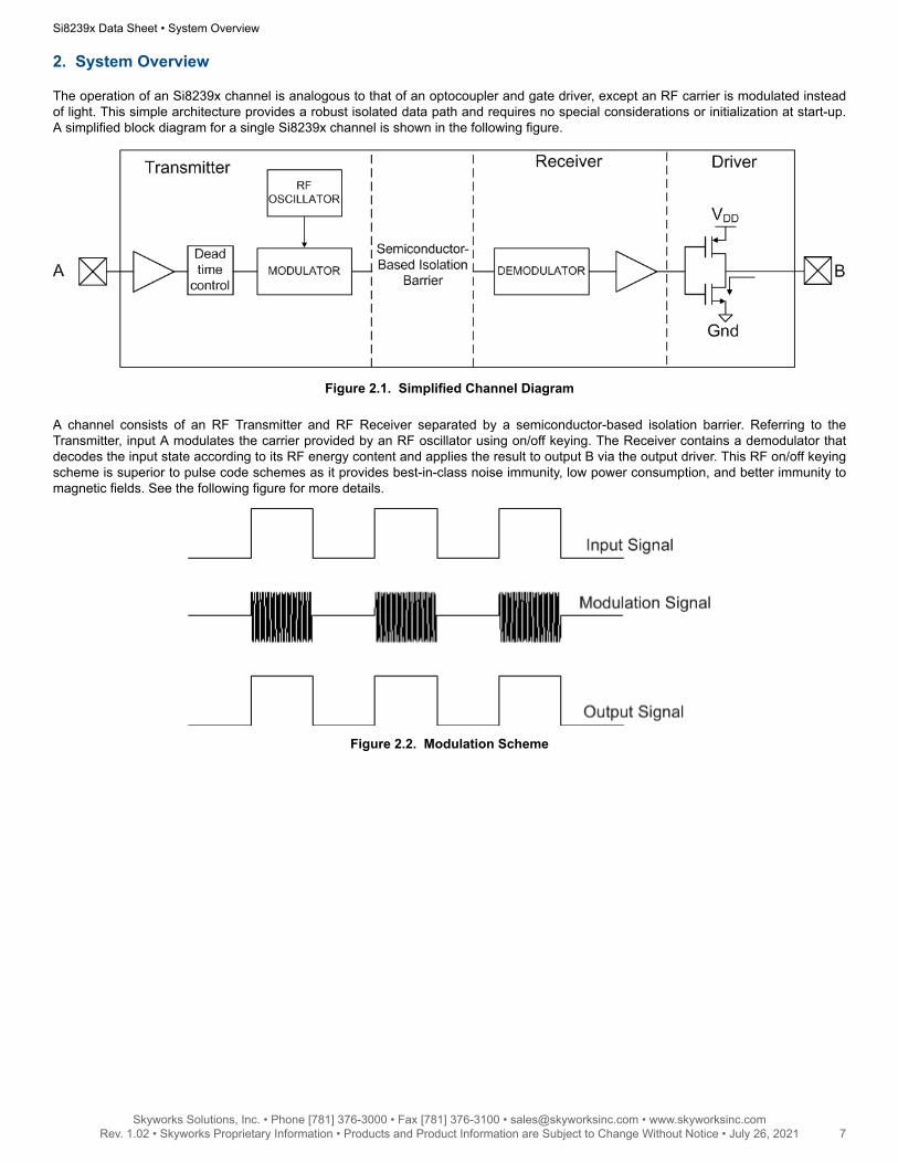
2. System Overview
The operation of an Si8239x channel is analogous to that of an optocoupler and gate driver, except an RF carrier is modulated insteadof light. This simple architecture provides a robust isolated data path and requires no special considerations or initialization at start-up.A simplified block diagram for a single Si8239x channel is shown in the following figure.
Figure 2.1. Simplified Channel Diagram
A channel consists of an RF Transmitter and RF Receiver separated by a semiconductor-based isolation barrier. Referring to theTransmitter, input A modulates the carrier provided by an RF oscillator using on/off keying. The Receiver contains a demodulator thatdecodes the input state according to its RF energy content and applies the result to output B via the output driver. This RF on/off keyingscheme is superior to pulse code schemes as it provides best-in-class noise immunity, low power consumption, and better immunity tomagnetic fields. See the following figure for more details.
Figure 2.2. Modulation Scheme
Si8239x Data Sheet • System Overview
Skyworks Solutions, Inc. • Phone [781] 376-3000 • Fax [781] 376-3100 • [email protected] • www.skyworksinc.com7 Rev. 1.02 • Skyworks Proprietary Information • Products and Product Information are Subject to Change Without Notice • July 26, 2021 7
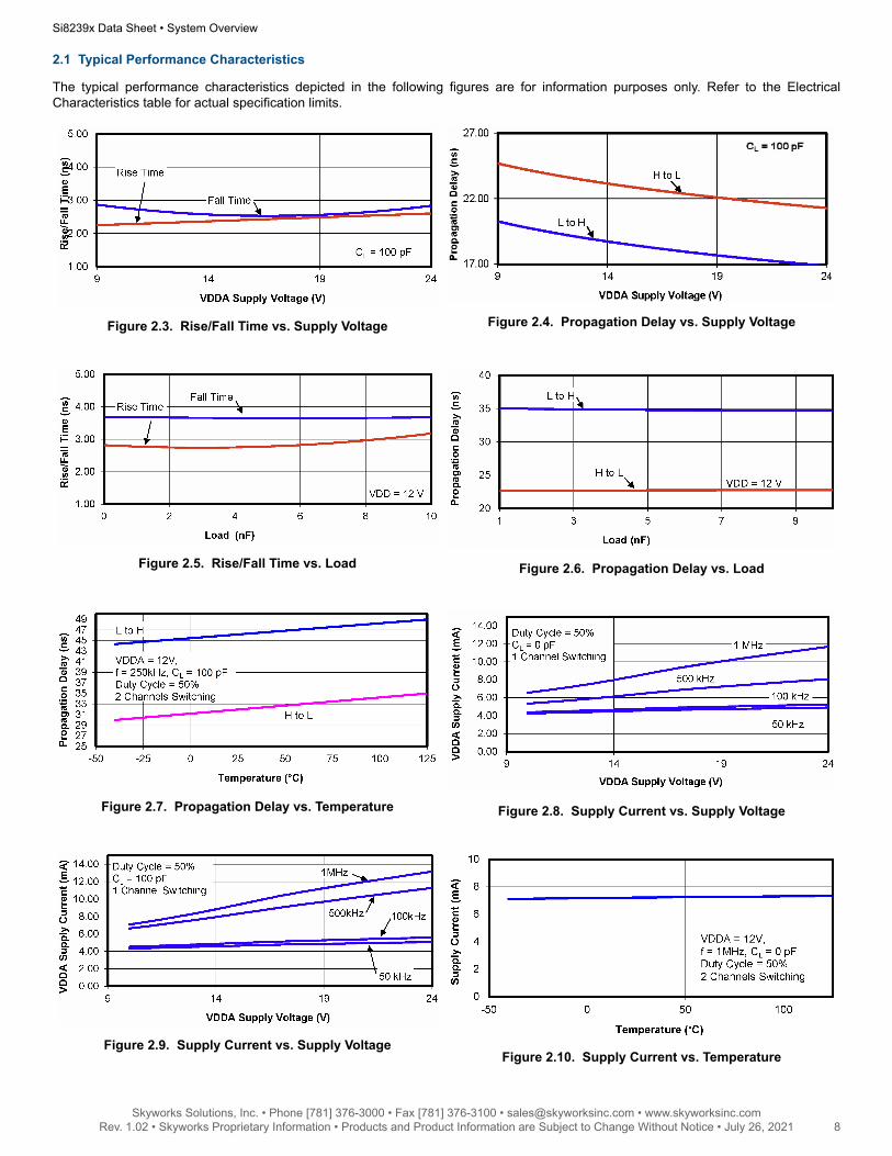
2.1 Typical Performance Characteristics
The typical performance characteristics depicted in the following figures are for information purposes only. Refer to the ElectricalCharacteristics table for actual specification limits.
Figure 2.3. Rise/Fall Time vs. Supply Voltage Figure 2.4. Propagation Delay vs. Supply Voltage
Figure 2.5. Rise/Fall Time vs. Load Figure 2.6. Propagation Delay vs. Load
Figure 2.7. Propagation Delay vs. Temperature Figure 2.8. Supply Current vs. Supply Voltage
Figure 2.9. Supply Current vs. Supply VoltageFigure 2.10. Supply Current vs. Temperature
Si8239x Data Sheet • System Overview
Skyworks Solutions, Inc. • Phone [781] 376-3000 • Fax [781] 376-3100 • [email protected] • www.skyworksinc.com8 Rev. 1.02 • Skyworks Proprietary Information • Products and Product Information are Subject to Change Without Notice • July 26, 2021 8
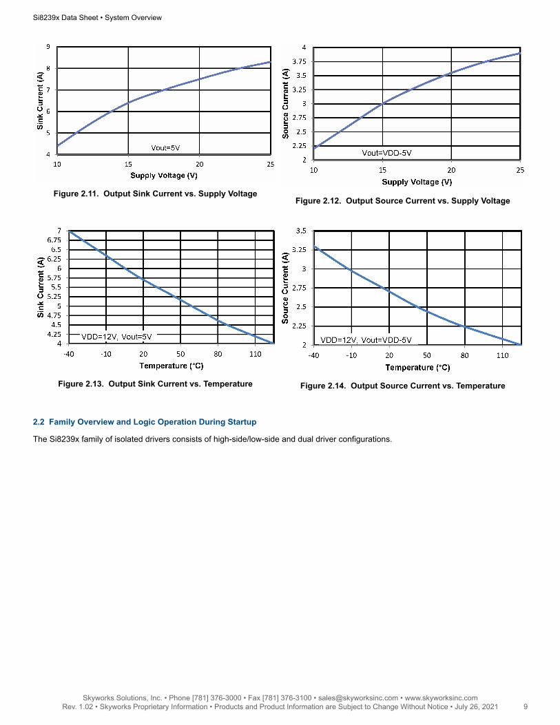
Figure 2.11. Output Sink Current vs. Supply VoltageFigure 2.12. Output Source Current vs. Supply Voltage
Figure 2.13. Output Sink Current vs. Temperature Figure 2.14. Output Source Current vs. Temperature
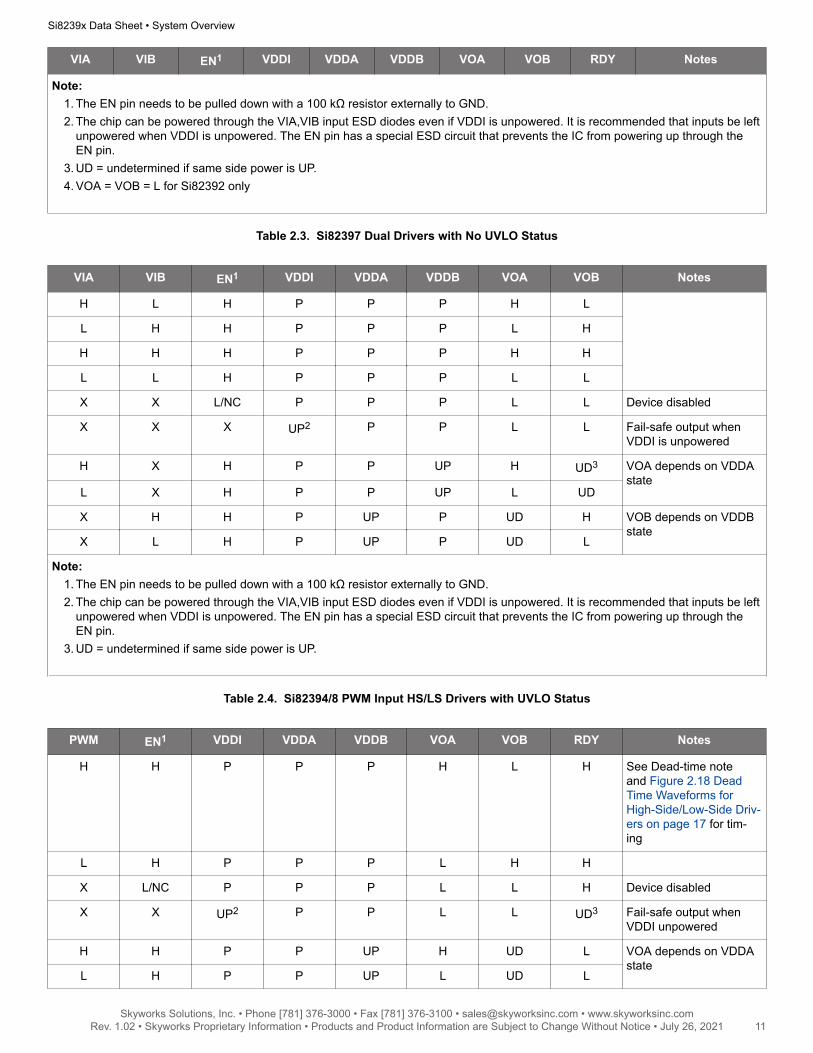
2.2 Family Overview and Logic Operation During Startup
The Si8239x family of isolated drivers consists of high-side/low-side and dual driver configurations.
Si8239x Data Sheet • System Overview
Skyworks Solutions, Inc. • Phone [781] 376-3000 • Fax [781] 376-3100 • [email protected] • www.skyworksinc.com9 Rev. 1.02 • Skyworks Proprietary Information • Products and Product Information are Subject to Change Without Notice • July 26, 2021 9

2.2.1 Device Behavior
The following are truth tables for the Si8239x families.
Table 2.1. Si82390/1/3 Drivers Enhanced UVLO and Status
VIA VIB EN1 VDDI VDDA VDDB VOA VOB RDY Notes
H L H P2 P P H L H
L H H P P P L H H
H H H P P P H / L4 H / L4 H
L L H P P P L L H
X X L/NC P P P L L H Device disabled
X X X UP2 P P L L UD3 Fail-safe output whenVDDI unpowered
X X H P P UP L UD L VOA, VOB are active-ly driven low if eitherVDDA or VDDB is UPX X H P UP P UD L L
Note:1. The EN pin needs to be pulled down with a 100 kΩ resistor externally to GND.2. The chip can be powered through the VIA,VIB input ESD diodes even if VDDI is unpowered. It is recommended that inputs be left
unpowered when VDDI is unpowered. The EN pin has a special ESD circuit that prevents the IC from powering up through theEN pin.
3. UD = undetermined if same side power is UP.4. VOA = VOB = L for Si82393 only
Table 2.2. Si82392/5/6 Drivers with UVLO Status
VIA VIB EN1 VDDI VDDA VDDB VOA VOB RDY Notes
H L H P P P H L H
L H H P P P L H H
H H H P P P H / L4 H / L4 H
L L H P P P L L H
X X L/NC P P P L L H Device disabled
X X X UP2 P P L L UD3 Fail-safe output whenVDDI unpowered
H X H P P UP H UD L VOA depends onVDDA state
L X H P P UP L UD L
X H H P UP P UD H L VOB depends onVDDB state
X L H P UP P UD L L
Si8239x Data Sheet • System Overview
Skyworks Solutions, Inc. • Phone [781] 376-3000 • Fax [781] 376-3100 • [email protected] • www.skyworksinc.com10 Rev. 1.02 • Skyworks Proprietary Information • Products and Product Information are Subject to Change Without Notice • July 26, 2021 10
VIA VIB EN1 VDDI VDDA VDDB VOA VOB RDY Notes
Note:1. The EN pin needs to be pulled down with a 100 kΩ resistor externally to GND.2. The chip can be powered through the VIA,VIB input ESD diodes even if VDDI is unpowered. It is recommended that inputs be left
unpowered when VDDI is unpowered. The EN pin has a special ESD circuit that prevents the IC from powering up through theEN pin.
3. UD = undetermined if same side power is UP.4. VOA = VOB = L for Si82392 only
Table 2.3. Si82397 Dual Drivers with No UVLO Status
VIA VIB EN1 VDDI VDDA VDDB VOA VOB Notes
H L H P P P H L
L H H P P P L H
H H H P P P H H
L L H P P P L L
X X L/NC P P P L L Device disabled
X X X UP2 P P L L Fail-safe output whenVDDI is unpowered
H X H P P UP H UD3 VOA depends on VDDAstate
L X H P P UP L UD
X H H P UP P UD H VOB depends on VDDBstate
X L H P UP P UD L
Note:1. The EN pin needs to be pulled down with a 100 kΩ resistor externally to GND.2. The chip can be powered through the VIA,VIB input ESD diodes even if VDDI is unpowered. It is recommended that inputs be left
unpowered when VDDI is unpowered. The EN pin has a special ESD circuit that prevents the IC from powering up through theEN pin.
3. UD = undetermined if same side power is UP.
Table 2.4. Si82394/8 PWM Input HS/LS Drivers with UVLO Status
PWM EN1 VDDI VDDA VDDB VOA VOB RDY Notes
H H P P P H L H See Dead-time noteand Figure 2.18 DeadTime Waveforms forHigh-Side/Low-Side Driv-ers on page 17 for tim-ing
L H P P P L H H
X L/NC P P P L L H Device disabled
X X UP2 P P L L UD3 Fail-safe output whenVDDI unpowered
H H P P UP H UD L VOA depends on VDDAstate
L H P P UP L UD L
Si8239x Data Sheet • System Overview
Skyworks Solutions, Inc. • Phone [781] 376-3000 • Fax [781] 376-3100 • [email protected] • www.skyworksinc.com11 Rev. 1.02 • Skyworks Proprietary Information • Products and Product Information are Subject to Change Without Notice • July 26, 2021 11

PWM EN1 VDDI VDDA VDDB VOA VOB RDY Notes
H H P UP P UD L L VOB depends on VDDBstate
L H P UP P UD H L
Note:1. The EN pin needs to be pulled down with a 100 kΩ resistor externally to GND.2. The chip can be powered through the PWM input ESD diodes even if VDDI is unpowered. It is recommended that inputs be left
unpowered when VDDI is unpowered. The EN pin has a special ESD circuit that prevents the IC from powering up through theEN pin.
3. UD = undetermined if same side power is UP.
2.3 Power Supply Connections
Isolation requirements mandate separating VDDI from the driver supplies. The decoupling caps for these supplies must be placed asclose to the VDD and GND pins of the Si8239x as possible. The optimum values for these capacitors are 1 μF and 0.1 μF for VDDI and10 μF and 0.1 μF for each driver supply. Low effective series resistance (ESR) capacitors, such as Tantalum, are recommended.
Si8239x Data Sheet • System Overview
Skyworks Solutions, Inc. • Phone [781] 376-3000 • Fax [781] 376-3100 • [email protected] • www.skyworksinc.com12 Rev. 1.02 • Skyworks Proprietary Information • Products and Product Information are Subject to Change Without Notice • July 26, 2021 12
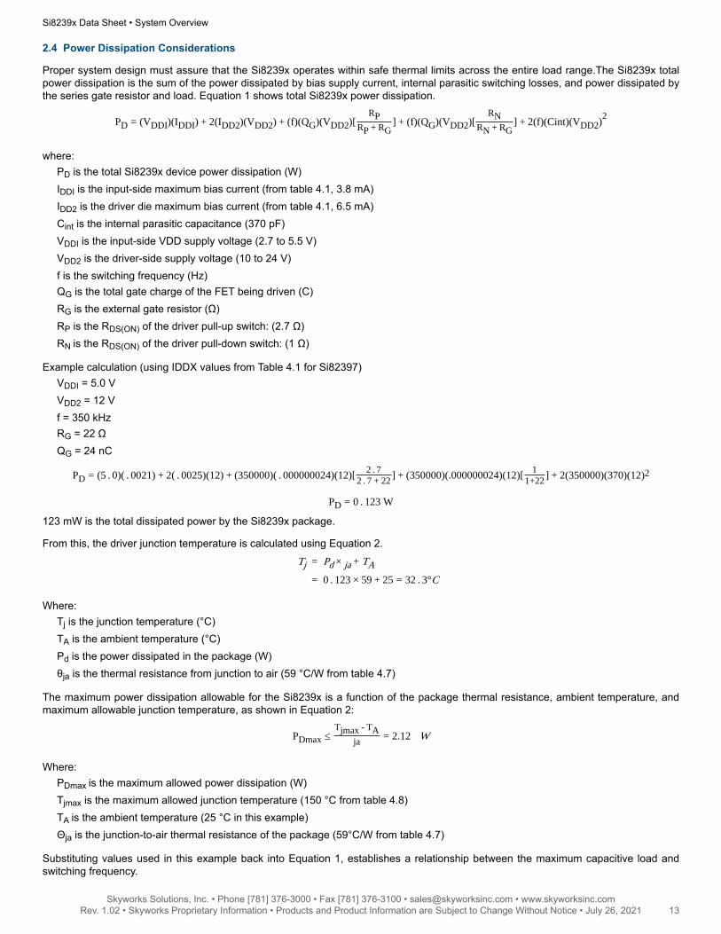
2.4 Power Dissipation Considerations
Proper system design must assure that the Si8239x operates within safe thermal limits across the entire load range.The Si8239x totalpower dissipation is the sum of the power dissipated by bias supply current, internal parasitic switching losses, and power dissipated bythe series gate resistor and load. Equation 1 shows total Si8239x power dissipation.
PD = (VDDI)(IDDI) + 2(IDD2)(VDD2) + (f)(QG)(VDD2)[RP
RP + RG] + (f)(QG)(VDD2)[
RNRN + RG
] + 2(f)(Cint)(VDD2)2
where:PD is the total Si8239x device power dissipation (W)IDDI is the input-side maximum bias current (from table 4.1, 3.8 mA)IDD2 is the driver die maximum bias current (from table 4.1, 6.5 mA)Cint is the internal parasitic capacitance (370 pF)VDDI is the input-side VDD supply voltage (2.7 to 5.5 V)VDD2 is the driver-side supply voltage (10 to 24 V)f is the switching frequency (Hz)QG is the total gate charge of the FET being driven (C)RG is the external gate resistor (Ω)RP is the RDS(ON) of the driver pull-up switch: (2.7 Ω)RN is the RDS(ON) of the driver pull-down switch: (1 Ω)
Example calculation (using IDDX values from Table 4.1 for Si82397)VDDI = 5.0 VVDD2 = 12 Vf = 350 kHzRG = 22 ΩQG = 24 nC
PD = (5 . 0)( . 0021) + 2( . 0025)(12) + (350000)( . 000000024)(12)[2 . 7
2 . 7 + 22 ] + (350000)(.000000024)(12)[1
1+22 ] + 2(350000)(370)(12)2
PD = 0 . 123 W
123 mW is the total dissipated power by the Si8239x package.
From this, the driver junction temperature is calculated using Equation 2.
Tj = Pd × ja + TA
= 0 . 123 × 59 + 25 = 32 . 3°C
Where:Tj is the junction temperature (°C)TA is the ambient temperature (°C)Pd is the power dissipated in the package (W)θja is the thermal resistance from junction to air (59 °C/W from table 4.7)
The maximum power dissipation allowable for the Si8239x is a function of the package thermal resistance, ambient temperature, andmaximum allowable junction temperature, as shown in Equation 2:
PDmax ≤Tjmax - TA
ja = 2.12 W
Where:PDmax is the maximum allowed power dissipation (W)Tjmax is the maximum allowed junction temperature (150 °C from table 4.8)TA is the ambient temperature (25 °C in this example)Θja is the junction-to-air thermal resistance of the package (59°C/W from table 4.7)
Substituting values used in this example back into Equation 1, establishes a relationship between the maximum capacitive load andswitching frequency.
Si8239x Data Sheet • System Overview
Skyworks Solutions, Inc. • Phone [781] 376-3000 • Fax [781] 376-3100 • [email protected] • www.skyworksinc.com13 Rev. 1.02 • Skyworks Proprietary Information • Products and Product Information are Subject to Change Without Notice • July 26, 2021 13
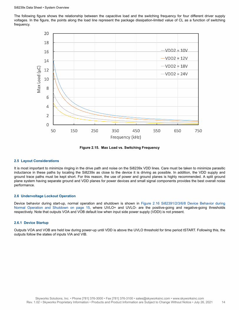
The following figure shows the relationship between the capacitive load and the switching frequency for four different driver supplyvoltages. In the figure, the points along the load line represent the package dissipation-limited value of CL as a function of switchingfrequency.
Figure 2.15. Max Load vs. Switching Frequency
2.5 Layout Considerations
It is most important to minimize ringing in the drive path and noise on the Si8239x VDD lines. Care must be taken to minimize parasiticinductance in these paths by locating the Si8239x as close to the device it is driving as possible. In addition, the VDD supply andground trace paths must be kept short. For this reason, the use of power and ground planes is highly recommended. A split groundplane system having separate ground and VDD planes for power devices and small signal components provides the best overall noiseperformance.
2.6 Undervoltage Lockout Operation
Device behavior during start-up, normal operation and shutdown is shown in Figure 2.16 Si82391/2/3/6/8 Device Behavior duringNormal Operation and Shutdown on page 15, where UVLO+ and UVLO- are the positive-going and negative-going thresholdsrespectively. Note that outputs VOA and VOB default low when input side power supply (VDDI) is not present.
2.6.1 Device Startup
Outputs VOA and VOB are held low during power-up until VDD is above the UVLO threshold for time period tSTART. Following this, theoutputs follow the states of inputs VIA and VIB.
Si8239x Data Sheet • System Overview
Skyworks Solutions, Inc. • Phone [781] 376-3000 • Fax [781] 376-3100 • [email protected] • www.skyworksinc.com14 Rev. 1.02 • Skyworks Proprietary Information • Products and Product Information are Subject to Change Without Notice • July 26, 2021 14

2.6.2 Undervoltage Lockout
Undervoltage Lockout (UVLO) is provided to prevent erroneous operation during device startup and shutdown or when VDD is below itsspecified operating circuits range. The input (control) side, Driver A and Driver B, each have their own undervoltage lockout monitors.
The Si8239x input side enters UVLO when VDDI < VDDIUV–, and exits UVLO when VDDI > VDDIUV+. The driver outputs, VOA andVOB, remain low when the input side of the Si8239x is in UVLO and their respective VDD supply (VDDA, VDDB) is within tolerance.Each driver output can enter or exit UVLO independently for the Si82394/5/6/7/8 products. For example, VOA unconditionally entersUVLO when VDDA falls below VDDAUV– and exits UVLO when VDDA rises above VDDAUV+. For the Si82390/1/3 products, wheneither VDDA or VDDB falls under VDDxUV–, this information is fed back through the isolation barrier to the input side logic whichforces VOB or VOA to be driven low respectively under these conditions. If the application is driving a transformer for an isolated powerconverter, for example, this behavior is useful to prevent flux imbalances in the transformer. Please note that this feature implies that itcan only be implemented when the VDDA and VDDB power supplies are independent from each other. If a bootstrap circuit is used forSi82390/1/3, it will prevent the IC from powering up. Do not use the Si82390/1/3 in conjunction with a bootstrap circuit for driver power.
Figure 2.16. Si82391/2/3/6/8 Device Behavior during Normal Operation and Shutdown
Si8239x Data Sheet • System Overview
Skyworks Solutions, Inc. • Phone [781] 376-3000 • Fax [781] 376-3100 • [email protected] • www.skyworksinc.com15 Rev. 1.02 • Skyworks Proprietary Information • Products and Product Information are Subject to Change Without Notice • July 26, 2021 15
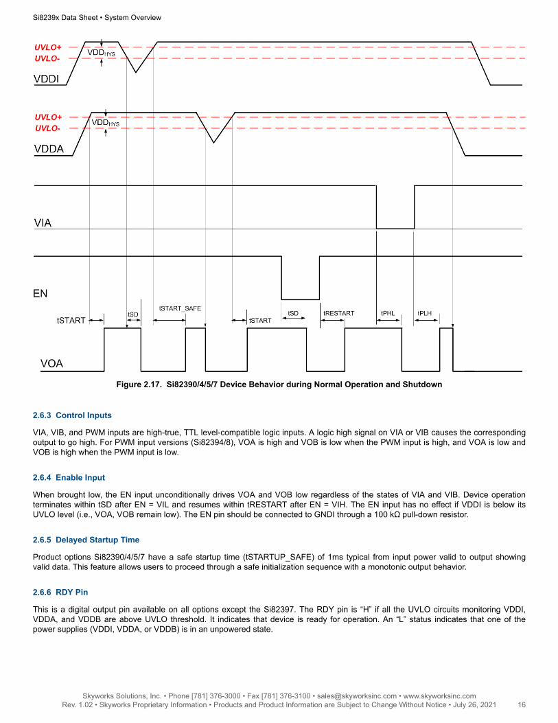
Figure 2.17. Si82390/4/5/7 Device Behavior during Normal Operation and Shutdown
2.6.3 Control Inputs
VIA, VIB, and PWM inputs are high-true, TTL level-compatible logic inputs. A logic high signal on VIA or VIB causes the correspondingoutput to go high. For PWM input versions (Si82394/8), VOA is high and VOB is low when the PWM input is high, and VOA is low andVOB is high when the PWM input is low.
2.6.4 Enable Input
When brought low, the EN input unconditionally drives VOA and VOB low regardless of the states of VIA and VIB. Device operationterminates within tSD after EN = VIL and resumes within tRESTART after EN = VIH. The EN input has no effect if VDDI is below itsUVLO level (i.e., VOA, VOB remain low). The EN pin should be connected to GNDI through a 100 kΩ pull-down resistor.
2.6.5 Delayed Startup Time
Product options Si82390/4/5/7 have a safe startup time (tSTARTUP_SAFE) of 1ms typical from input power valid to output showingvalid data. This feature allows users to proceed through a safe initialization sequence with a monotonic output behavior.
2.6.6 RDY Pin
This is a digital output pin available on all options except the Si82397. The RDY pin is “H” if all the UVLO circuits monitoring VDDI,VDDA, and VDDB are above UVLO threshold. It indicates that device is ready for operation. An “L” status indicates that one of thepower supplies (VDDI, VDDA, or VDDB) is in an unpowered state.
Si8239x Data Sheet • System Overview
Skyworks Solutions, Inc. • Phone [781] 376-3000 • Fax [781] 376-3100 • [email protected] • www.skyworksinc.com16 Rev. 1.02 • Skyworks Proprietary Information • Products and Product Information are Subject to Change Without Notice • July 26, 2021 16
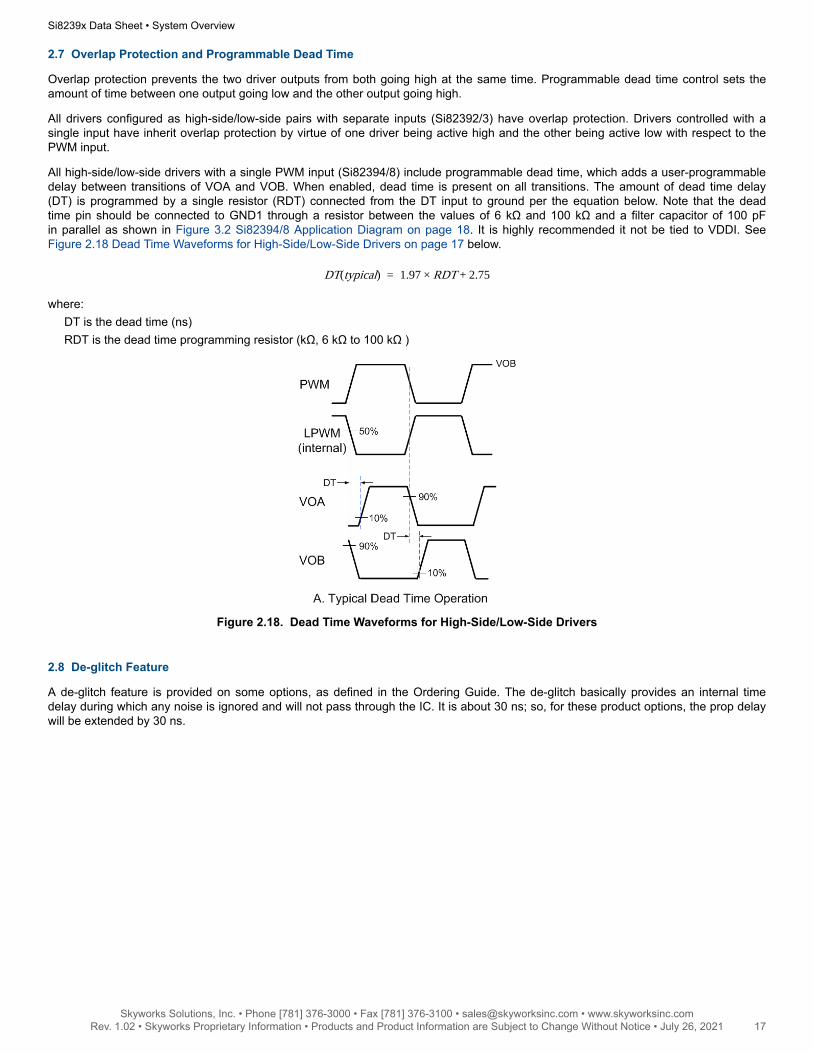
2.7 Overlap Protection and Programmable Dead Time
Overlap protection prevents the two driver outputs from both going high at the same time. Programmable dead time control sets theamount of time between one output going low and the other output going high.
All drivers configured as high-side/low-side pairs with separate inputs (Si82392/3) have overlap protection. Drivers controlled with asingle input have inherit overlap protection by virtue of one driver being active high and the other being active low with respect to thePWM input.
All high-side/low-side drivers with a single PWM input (Si82394/8) include programmable dead time, which adds a user-programmabledelay between transitions of VOA and VOB. When enabled, dead time is present on all transitions. The amount of dead time delay(DT) is programmed by a single resistor (RDT) connected from the DT input to ground per the equation below. Note that the deadtime pin should be connected to GND1 through a resistor between the values of 6 kΩ and 100 kΩ and a filter capacitor of 100 pFin parallel as shown in Figure 3.2 Si82394/8 Application Diagram on page 18. It is highly recommended it not be tied to VDDI. SeeFigure 2.18 Dead Time Waveforms for High-Side/Low-Side Drivers on page 17 below.
DT(typical) = 1.97 × RDT + 2.75
where:DT is the dead time (ns)RDT is the dead time programming resistor (kΩ, 6 kΩ to 100 kΩ )
Figure 2.18. Dead Time Waveforms for High-Side/Low-Side Drivers
2.8 De-glitch Feature
A de-glitch feature is provided on some options, as defined in the Ordering Guide. The de-glitch basically provides an internal timedelay during which any noise is ignored and will not pass through the IC. It is about 30 ns; so, for these product options, the prop delaywill be extended by 30 ns.
Si8239x Data Sheet • System Overview
Skyworks Solutions, Inc. • Phone [781] 376-3000 • Fax [781] 376-3100 • [email protected] • www.skyworksinc.com17 Rev. 1.02 • Skyworks Proprietary Information • Products and Product Information are Subject to Change Without Notice • July 26, 2021 17

3. Applications
The following examples illustrate typical circuit configurations using the Si8239x.
3.1 High-Side/Low-Side Driver
The Si82392 and Si82393 devices are high-side/low-side type drivers controlled by separate driver signals, VIA and VIB.
Si82392/3
VIA VDDA
VOA
VOB
VDDB
GNDB
EN
CONTROLLER
VIB
OUT 1
OUT 2
I/O
VDDB
GNDI
VDDI VDDI
C1 1 µF
C2 0 .1 µF
C5 0 .1 µF
C6 10 µF
RDY I/O
RPD
Q1
VDDA
C3 0 .1 µF
C4 10 µF
Q2
Figure 3.1. Si82392/3 Application Diagram
The following figure shows the Si82394/8 controlled by a single PWM signal.
Figure 3.2. Si82394/8 Application Diagram
In the above figure, D1 and CB form a conventional bootstrap circuit that allows VOA to operate as a high-side driver for Q1, whichhas a maximum drain voltage of 1500 V. VOB is connected as a conventional low-side driver. Note that the input side of the Si8239xrequires VDDI in the range of 2.5 to 5.5 V, while the VDDA and VDDB output side supplies must be between 6.5 and 24 V with respectto their respective grounds. The bootstrap start up time will depend on the CB cap chosen. Also note that the bypass capacitors on theSi8239x should be located as close to the chip as possible.
Si8239x Data Sheet • Applications
Skyworks Solutions, Inc. • Phone [781] 376-3000 • Fax [781] 376-3100 • [email protected] • www.skyworksinc.com18 Rev. 1.02 • Skyworks Proprietary Information • Products and Product Information are Subject to Change Without Notice • July 26, 2021 18
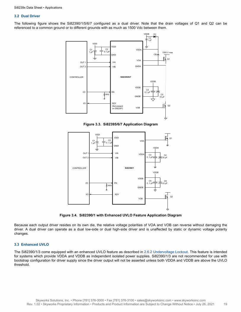
3.2 Dual Driver
The following figure shows the Si82390/1/5/6/7 configured as a dual driver. Note that the drain voltages of Q1 and Q2 can bereferenced to a common ground or to different grounds with as much as 1500 Vdc between them.
Si82395/6/7
VIA
VDDA
VOA
GNDA
VOB
VDDB
GNDB
EN
CONTROLLER
VIB
OUT 1
OUT 2
I/O
Q1
Q2
VDDB
GNDI
VDDIVDDI
C11 µF
C20.1 µF
C40.1 µF
C510 µF
RDYI/O
RPD
CB
D1VDDB
C31 µF
1500 V max
(Not present on Si82397)
Figure 3.3. Si82395/6/7 Application Diagram
Si82390/1
VIA VDDA
VOA
VOB
VDDB
GNDB
EN
CONTROLLER
VIB
OUT 1
OUT 2
I/O
VDDB
GNDI
VDDI VDDI
C1 1 µF
C2 0 .1 µF
C5 0 .1 µF
C6 10 µF
RDY I/O
RPD
Q1
VDDA
C3 0 .1 µF
C4 10 µF
Q2
Figure 3.4. Si82390/1 with Enhanced UVLO Feature Application Diagram
Because each output driver resides on its own die, the relative voltage polarities of VOA and VOB can reverse without damaging thedriver. A dual driver can operate as a dual low-side or dual high-side driver and is unaffected by static or dynamic voltage polaritychanges.
3.3 Enhanced UVLO
The Si82390/1/3 come equipped with an enhanced UVLO feature as described in 2.6.2 Undervoltage Lockout. This feature is intendedfor systems which provide VDDA and VDDB as independent isolated power supplies. Si82390/1/3 are not recommended for use withbootstrap configuration for driver supply since the driver output will not be asserted unless both VDDA and VDDB are above the UVLOthreshold.
Si8239x Data Sheet • Applications
Skyworks Solutions, Inc. • Phone [781] 376-3000 • Fax [781] 376-3100 • [email protected] • www.skyworksinc.com19 Rev. 1.02 • Skyworks Proprietary Information • Products and Product Information are Subject to Change Without Notice • July 26, 2021 19
4. Electrical Characteristics
Table 4.1. Electrical Characteristics1,2
Parameter Symbol Test Condition Min Typ Max Unit
DC Specifications
Input-side Power Supply Voltage VDDI 2.5 3.3 5.5 V
Driver Supply Voltage VDDA, VDDB Voltage between VDDA andGNDA, and VDDB and
GNDB
6.5 — 24 V
Input Supply Quiescent Current EN = 0 IDDI(Q) Si82390/1/2/3/4/5/6/8 — 2.8 3.8 mA
Si82397 — 1.5 2.1 mA
Output Supply Quiescent Current, perchannel EN = 0
IDDA(Q),IDDB(Q)
Si82390/1/2/3/4/5/6/8 — 4.2 6.5 mA
Si82397 — 1.5 2.5 mA
Input Supply Active Current IDDI Si82390/1/2/3/5/6 VIA, VIBfreq = 1 MHz
— 5.0 7.2 mA
Si82394/8: PWM freq = 1MHz
— 5.2 7.3
Si82397: VIA, VIB freq = 1MHz
— 3.7 5.6
Output Supply Active Current, perchannel
IDDA/B Si82390/1/2/3/4/5/6/8: Inputfreq = 1 MHz, no load
— 7.1 16.0 mA
Si82397: Input freq = 1 MHz,no load
— 4.4 12.4
Digital Parameters
Input Pin Leakage Current, VIA, VIB,PWM
IVIA, IVIB, IPWM –10 — +10 µA
Input Pin Leakage Current, EN IENABLE –10 — +10 µA
Logic High Input Threshold VIH TTL Levels 2.0 — — V
Logic Low Input Threshold VIL TTL Levels — — 0.8 V
Input Hysteresis VIHYST 400 450 — mV
High Level Output Voltage (RDY pinonly)
VOH IOH = –4 mA VDDI -0.4
4.8 — V
Low Level Output Voltage (RDY pin on-ly)
VOL IOL = 4 mA — 0.2 0.4 V
Drive Parameters
Logic High Output Voltage VOAH, VOBH IOA, IOB = –1 mA VDDA,VDDB –
0.04
— — V
Logic Low Output Voltage VOAL, VOBL IOA, IOB = 1 mA — — 0.04 V
Output Short-Circuit Pulsed SourceCurrent
IOA(SCL),IOB(SCL)
See Figure 4.1 IOL Sink Cur-rent Test on page 23
— 4.0 — A
Output Short-Circuit Pulsed SourceCurrent
IOA(SCH),IOB(SCH)
See Figure 4.2 IOH SourceCurrent Test on page 23
— 2.0 — A
Si8239x Data Sheet • Electrical Characteristics
Skyworks Solutions, Inc. • Phone [781] 376-3000 • Fax [781] 376-3100 • [email protected] • www.skyworksinc.com20 Rev. 1.02 • Skyworks Proprietary Information • Products and Product Information are Subject to Change Without Notice • July 26, 2021 20

Parameter Symbol Test Condition Min Typ Max Unit
Output Sink Resistance RON(SINK) — 1.0 — Ω
Output Source Resistance RON(SOURCE) — 2.7 — Ω
VDDI Undervoltage Threshold VDDIUV+ VDDI rising 2.15 2.3 2.5 V
VDDI Undervoltage Threshold VDDIUV– VDDI falling 2.1 2.2 2.4 V
VDDI Lockout Hysteresis VDDIHYS 80 100 — mV
VDDA, VDDB Undervoltage Threshold VDDAUV+,VDDBUV+
VDDA, VDDB rising V
6 V 5.0 6.0 7.0
8 V 7.2 8.6 10.0
12 V 9.2 11.1 12.8
VDDA, VDDB Undervoltage Threshold VDDAUV–,VDDBUV–
VDDA, VDDB falling V
6 V 4.7 5.8 6.7
8 V 6.6 8.0 9.3
12 V 8.7 10.1 11.6
VDDA, VDDB Lockout Hysteresis VDDAHYS,VDDBHYS
UVLO = 6 V
UVLO = 8 V
UVLO = 12 V
200
450
600
280
600
1000
—
—
—
mV
AC Specifications
UVLO Fault Shutdown Time EnhancedMode
Si82390/1/3 only
VDDAUV– to VOB low
VDDBUV– to VOA low
— 120 — ns
UVLO Fault Shutdown Time VDDAUV– to VOA low
VDDBUV– to VOB low
— 10 — ns
UVLO fault to RDY t_FLT — 92 — ns
Minimum Pulse Width — 30 — ns
Propagation Delay tpHL, tpLH Si82390/1/2/3/5/6/7 (with node-glitch)
20 30 40 ns
VDDA/B = 12 V tpHL Si82394/8 (with no de-glitch) 20 30 40 ns
CL = 0 pF tpLH Si82394/8 (with no de-glitch;measured with 6 kΩ RDT
resistor; includes minimumdead time)
35 45 55 ns
tpHL Si82394xx4/8xx4 (have de-glitch)
60 77 95 ns
tpLH Si82394xx4/8xx4 (have de-glitch and measured with 6kΩ RDT resistor; includes
minimum dead time and de-glitch delay)
99 116 135 ns
Si8239x Data Sheet • Electrical Characteristics
Skyworks Solutions, Inc. • Phone [781] 376-3000 • Fax [781] 376-3100 • [email protected] • www.skyworksinc.com21 Rev. 1.02 • Skyworks Proprietary Information • Products and Product Information are Subject to Change Without Notice • July 26, 2021 21
Parameter Symbol Test Condition Min Typ Max Unit
Pulse Width Distortion |tPLH – tPHL| PWD VDDA/B = 12 V
CL = 0 pF
— 2.7 5.60 ns
Programmed Dead Time for productoptions with 40–600 ns dead time set-ting range
DT RDT = 6 kΩ
RDT = 15 kΩ
RDT = 100 kΩ
27
70
450
38
90
590
57
130
750
ns
Output Rise and Fall Time tR,tF CL = 200 pF — — 12 ns
Shutdown Time from Enable False tSD All options with no de-glitch — — 60 ns
All options with de-glitch — — 113
Restart Time from Enable True tRESTART All options with no de-glitch — — 60 ns
All options with de-glitch — — 95
Device Start-up Time Input Time from VDDI_ =VDDI_UV+ to VOA, VOB =
VIA, VIB
— —
Si82390/4/5/7 tSTART_SAFE 1 ms
Si82391/2/3/6/8 tSTART 40 µs
Device Start-up Time
Output
tSTART_OUT Time from VDDA/B = VDDA/B_UV+ to VOA, VOB = VIA,
VIB
— 60 — µs
Common Mode Transient Immunity CMTI VIA, VIB, PWM = VDDI or 0V
VCM = 1500 V
35 100 — kV/µs
Note:1. 2.5 V < VDDI < 5.5 V; 6.5 V < VDDA, VDDB < 24 V; TA = –40 to +125 °C.2. Typical specs at 25 °C, VDDA = VDDB = 12 V for 5 V and 8 V UVLO devices, otherwise 15 V.
Si8239x Data Sheet • Electrical Characteristics
Skyworks Solutions, Inc. • Phone [781] 376-3000 • Fax [781] 376-3100 • [email protected] • www.skyworksinc.com22 Rev. 1.02 • Skyworks Proprietary Information • Products and Product Information are Subject to Change Without Notice • July 26, 2021 22
The following figures depict sink current, source current, and common-mode transient immunity test circuits, respectively.
Figure 4.1. IOL Sink Current Test
Figure 4.2. IOH Source Current Test
Si8239x Data Sheet • Electrical Characteristics
Skyworks Solutions, Inc. • Phone [781] 376-3000 • Fax [781] 376-3100 • [email protected] • www.skyworksinc.com23 Rev. 1.02 • Skyworks Proprietary Information • Products and Product Information are Subject to Change Without Notice • July 26, 2021 23
Figure 4.3. CMTI Test Circuit
Table 4.2. Regulatory Information1,2,3
CSA
The Si8239x is certified under CSA. For more details, see Master Contract File 232873.
60950-1, 62368-1: Up to 600 VRMS reinforced insulation working voltage; up to 1000 VRMS basic insulation working voltage.
VDE
The Si8239x is certified according to VDE 0884-10. For more details, see File 5006301-4880-0001.
VDE 0884-10: Up to 891 Vpeak for basic insulation working voltage.
60950-1, 62368-1: Up to 600 VRMS reinforced insulation working voltage; up to 1000 VRMS basic insulation working voltage.
UL
The Si8239x is certified under UL1577 component recognition program. For more details, see File E257455.
Rated up to 5000 VRMS isolation voltage for basic protection.
CQC
The Si8239x is certified under GB4943.1-2011.
Rated up to 600 VRMS reinforced insulation working voltage; up to 1000 VRMS basic insulation working voltage.
Note:1. Regulatory Certifications apply to 2.5 kVRMS rated devices which are production tested to 3.0 kVRMS for 1 sec.2. Regulatory Certifications apply to 5.0 kVRMS rated devices which are production tested to 6.0 kVRMS for 1 sec.3. For more information, see Ordering Guide.
Si8239x Data Sheet • Electrical Characteristics
Skyworks Solutions, Inc. • Phone [781] 376-3000 • Fax [781] 376-3100 • [email protected] • www.skyworksinc.com24 Rev. 1.02 • Skyworks Proprietary Information • Products and Product Information are Subject to Change Without Notice • July 26, 2021 24
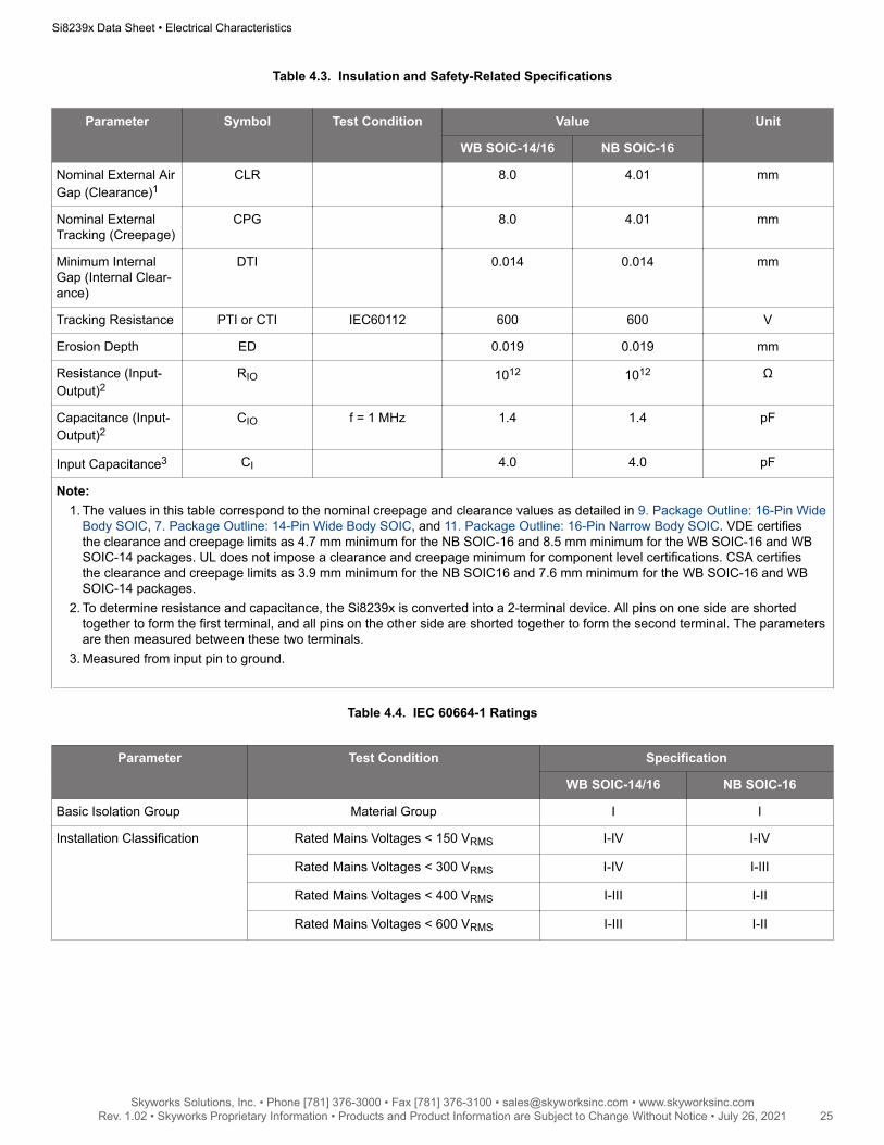
Table 4.3. Insulation and Safety-Related Specifications
Parameter Symbol Test Condition Value Unit
WB SOIC-14/16 NB SOIC-16
Nominal External AirGap (Clearance)1
CLR 8.0 4.01 mm
Nominal ExternalTracking (Creepage)
CPG 8.0 4.01 mm
Minimum InternalGap (Internal Clear-ance)
DTI 0.014 0.014 mm
Tracking Resistance PTI or CTI IEC60112 600 600 V
Erosion Depth ED 0.019 0.019 mm
Resistance (Input-Output)2
RIO 1012 1012 Ω
Capacitance (Input-Output)2
CIO f = 1 MHz 1.4 1.4 pF
Input Capacitance3 CI 4.0 4.0 pF
Note:1. The values in this table correspond to the nominal creepage and clearance values as detailed in 9. Package Outline: 16-Pin Wide
Body SOIC, 7. Package Outline: 14-Pin Wide Body SOIC, and 11. Package Outline: 16-Pin Narrow Body SOIC. VDE certifiesthe clearance and creepage limits as 4.7 mm minimum for the NB SOIC-16 and 8.5 mm minimum for the WB SOIC-16 and WBSOIC-14 packages. UL does not impose a clearance and creepage minimum for component level certifications. CSA certifiesthe clearance and creepage limits as 3.9 mm minimum for the NB SOIC16 and 7.6 mm minimum for the WB SOIC-16 and WBSOIC-14 packages.
2. To determine resistance and capacitance, the Si8239x is converted into a 2-terminal device. All pins on one side are shortedtogether to form the first terminal, and all pins on the other side are shorted together to form the second terminal. The parametersare then measured between these two terminals.
3. Measured from input pin to ground.
Table 4.4. IEC 60664-1 Ratings
Parameter Test Condition Specification
WB SOIC-14/16 NB SOIC-16
Basic Isolation Group Material Group I I
Installation Classification Rated Mains Voltages < 150 VRMS I-IV I-IV
Rated Mains Voltages < 300 VRMS I-IV I-III
Rated Mains Voltages < 400 VRMS I-III I-II
Rated Mains Voltages < 600 VRMS I-III I-II
Si8239x Data Sheet • Electrical Characteristics
Skyworks Solutions, Inc. • Phone [781] 376-3000 • Fax [781] 376-3100 • [email protected] • www.skyworksinc.com25 Rev. 1.02 • Skyworks Proprietary Information • Products and Product Information are Subject to Change Without Notice • July 26, 2021 25

Table 4.5. VDE0884-10 Insulation Characteristics
Parameter Symbol Test Condition Characteristic Unit
WB SOIC-14/16 NB SOIC-16
Maximum WorkingInsulation Voltage
VIORM 891 560 V peak
Input to Output TestVoltage
VPR Method b1 (VIORM x1.875 = VPR, 100%Production Test, tm= 1 sec, Partial Dis-
charge < 5 pC)
1671 1050 V peak
Transient Overvolt-age
VIOTM t = 60 sec 6000 4000 V peak
Surge Voltage VIOSM Tested per IEC60065 with surge
voltage of 1.2μs/50μs
Si8239xxB/D testedwith 4000 V
3077 3077 V peak
Pollution Degree(DIN VDE 0110, SeeTable 4.1 ElectricalCharacteristics1,2 onpage 20)
2 2
Insulation Resist-ance at TS, VIO =500 V
RS >109 >109 Ω
Note:1. Maintenance of the safety data is ensured by protective circuits. The Si8239x provides a climate classification of 40/125/21.
Table 4.6. IEC Safety Limiting Values1
Parameter Symbol Test Condition WB SOIC-14/16 NB SOIC-16 Unit
Safety Temperature TS 150 150 °C
Safety Input Current IS θJA = 59 °C/W (WB SO-IC-14/16), 63 °C/W (NB
SOIC-16)
VDDI = 5.5 V,
VDDA = VDDB = 24 V,
TJ = 150 °C, TA = 25 °C
88 83 mA
Device Power Dissi-pation2
PD 2.1 2.0 W
Si8239x Data Sheet • Electrical Characteristics
Skyworks Solutions, Inc. • Phone [781] 376-3000 • Fax [781] 376-3100 • [email protected] • www.skyworksinc.com26 Rev. 1.02 • Skyworks Proprietary Information • Products and Product Information are Subject to Change Without Notice • July 26, 2021 26
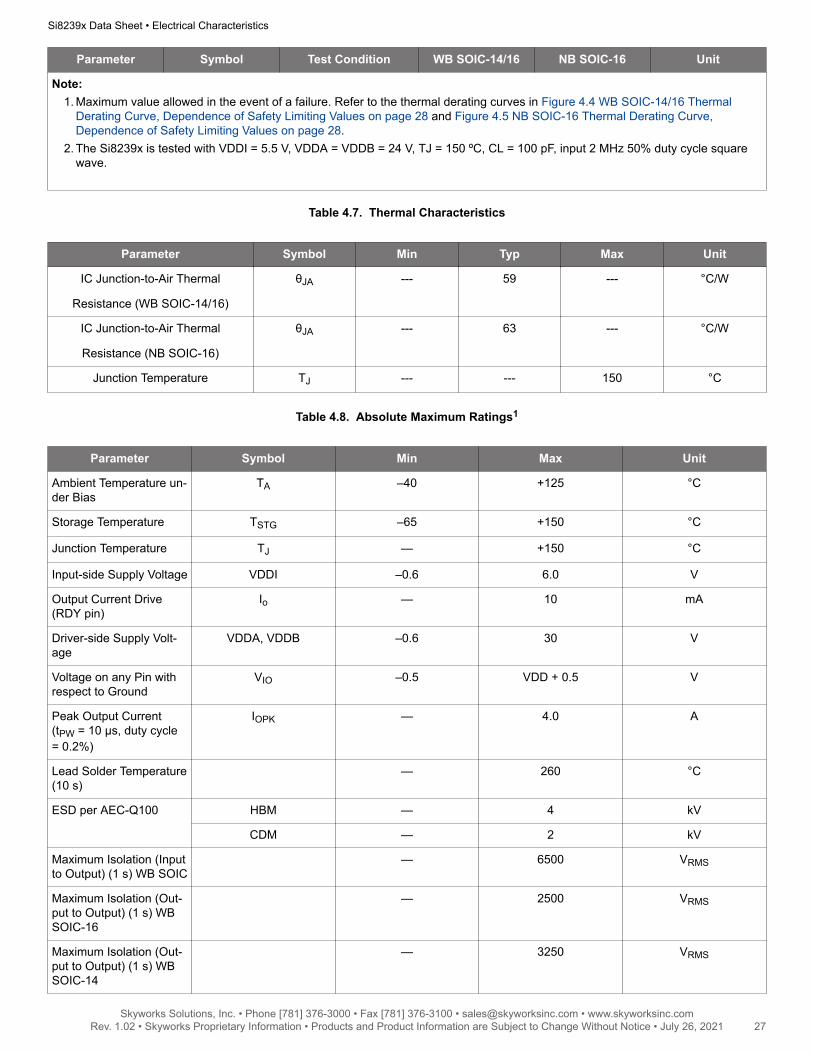
Parameter Symbol Test Condition WB SOIC-14/16 NB SOIC-16 Unit
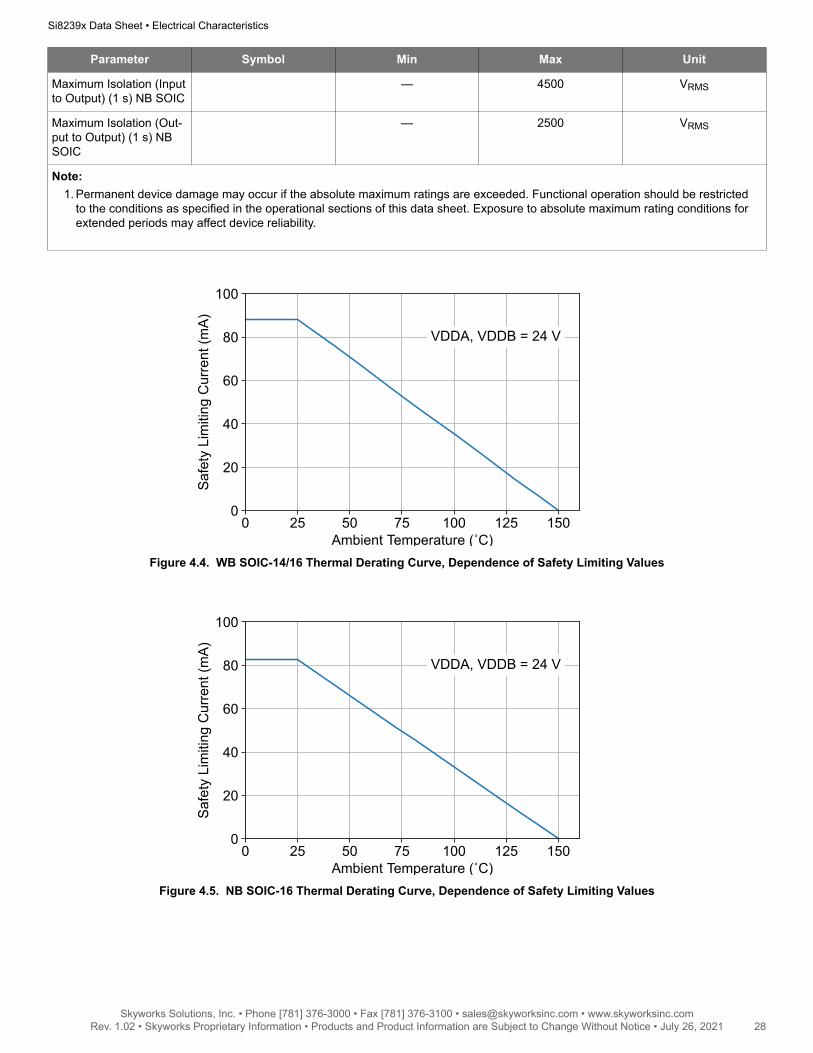
Note:1. Maximum value allowed in the event of a failure. Refer to the thermal derating curves in Figure 4.4 WB SOIC-14/16 Thermal
Derating Curve, Dependence of Safety Limiting Values on page 28 and Figure 4.5 NB SOIC-16 Thermal Derating Curve,Dependence of Safety Limiting Values on page 28.
2. The Si8239x is tested with VDDI = 5.5 V, VDDA = VDDB = 24 V, TJ = 150 ºC, CL = 100 pF, input 2 MHz 50% duty cycle squarewave.
Table 4.7. Thermal Characteristics
Parameter Symbol Min Typ Max Unit
IC Junction-to-Air Thermal
Resistance (WB SOIC-14/16)
θJA --- 59 --- °C/W
IC Junction-to-Air Thermal
Resistance (NB SOIC-16)
θJA --- 63 --- °C/W
Junction Temperature TJ --- --- 150 °C
Table 4.8. Absolute Maximum Ratings1
Parameter Symbol Min Max Unit
Ambient Temperature un-der Bias
TA –40 +125 °C
Storage Temperature TSTG –65 +150 °C
Junction Temperature TJ — +150 °C
Input-side Supply Voltage VDDI –0.6 6.0 V
Output Current Drive(RDY pin)
Io — 10 mA
Driver-side Supply Volt-age
VDDA, VDDB –0.6 30 V
Voltage on any Pin withrespect to Ground
VIO –0.5 VDD + 0.5 V
Peak Output Current(tPW = 10 µs, duty cycle= 0.2%)
IOPK — 4.0 A
Lead Solder Temperature(10 s)
— 260 °C
ESD per AEC-Q100 HBM — 4 kV
CDM — 2 kV
Maximum Isolation (Inputto Output) (1 s) WB SOIC
— 6500 VRMS
Maximum Isolation (Out-put to Output) (1 s) WBSOIC-16
— 2500 VRMS
Maximum Isolation (Out-put to Output) (1 s) WBSOIC-14
— 3250 VRMS
Si8239x Data Sheet • Electrical Characteristics
Skyworks Solutions, Inc. • Phone [781] 376-3000 • Fax [781] 376-3100 • [email protected] • www.skyworksinc.com27 Rev. 1.02 • Skyworks Proprietary Information • Products and Product Information are Subject to Change Without Notice • July 26, 2021 27
Parameter Symbol Min Max Unit
Maximum Isolation (Inputto Output) (1 s) NB SOIC
— 4500 VRMS
Maximum Isolation (Out-put to Output) (1 s) NBSOIC
— 2500 VRMS
Note:1. Permanent device damage may occur if the absolute maximum ratings are exceeded. Functional operation should be restricted
to the conditions as specified in the operational sections of this data sheet. Exposure to absolute maximum rating conditions forextended periods may affect device reliability.
0 25 50 75 100 125 150Ambient Temperature (˚C)
0
20
40
60
80
100
Saf
ety
Lim
iting
Cur
rent
(mA
)
VDDA, VDDB = 24 V
Figure 4.4. WB SOIC-14/16 Thermal Derating Curve, Dependence of Safety Limiting Values
0 25 50 75 100 125 150Ambient Temperature (˚C)
0
20
40
60
80
100
Saf
ety
Lim
iting
Cur
rent
(mA
)
VDDA, VDDB = 24 V
Figure 4.5. NB SOIC-16 Thermal Derating Curve, Dependence of Safety Limiting Values
Si8239x Data Sheet • Electrical Characteristics
Skyworks Solutions, Inc. • Phone [781] 376-3000 • Fax [781] 376-3100 • [email protected] • www.skyworksinc.com28 Rev. 1.02 • Skyworks Proprietary Information • Products and Product Information are Subject to Change Without Notice • July 26, 2021 28

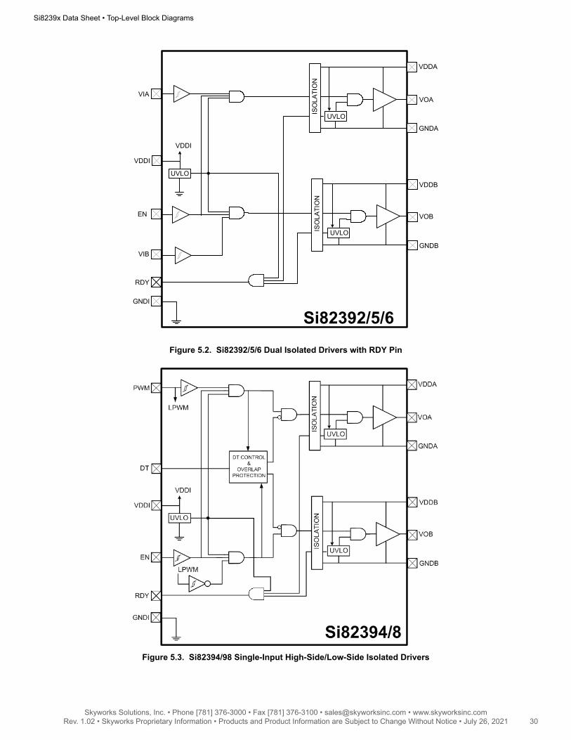
5. Top-Level Block Diagrams
UVLO
VDDA
VOA
GNDA
VOB
ISO
LATI
ON
VDDB
GNDB
UVLO
VIA
ISO
LATI
ON
UVLO
GNDI
VIB
VDDI
VDDI
EN
RDY
Si82390/1/3Figure 5.1. Si82390/1/3 Dual Isolated Drivers with Enhanced UVLO Safety
Si8239x Data Sheet • Top-Level Block Diagrams
Skyworks Solutions, Inc. • Phone [781] 376-3000 • Fax [781] 376-3100 • [email protected] • www.skyworksinc.com29 Rev. 1.02 • Skyworks Proprietary Information • Products and Product Information are Subject to Change Without Notice • July 26, 2021 29
UVLO
VDDA
VOA
GNDA
VOB
ISO
LATI
ON
VDDB
GNDB
UVLO
VIA
ISO
LATI
ON
UVLO
GNDI
VIB
VDDI
VDDI
EN
RDY
Si82392/5/6Figure 5.2. Si82392/5/6 Dual Isolated Drivers with RDY Pin
Figure 5.3. Si82394/98 Single-Input High-Side/Low-Side Isolated Drivers
Si8239x Data Sheet • Top-Level Block Diagrams
Skyworks Solutions, Inc. • Phone [781] 376-3000 • Fax [781] 376-3100 • [email protected] • www.skyworksinc.com30 Rev. 1.02 • Skyworks Proprietary Information • Products and Product Information are Subject to Change Without Notice • July 26, 2021 30

Figure 5.4. Si82397 Dual Isolated Drivers
Si8239x Data Sheet • Top-Level Block Diagrams
Skyworks Solutions, Inc. • Phone [781] 376-3000 • Fax [781] 376-3100 • [email protected] • www.skyworksinc.com31 Rev. 1.02 • Skyworks Proprietary Information • Products and Product Information are Subject to Change Without Notice • July 26, 2021 31
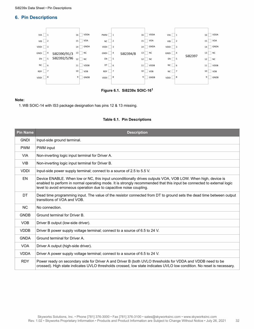
6. Pin Descriptions
VDDA
VOA
GNDA
NC
NC
VDDB
VOB
GNDB
Si82394/8
VDDI
PWM
NC
GNDI
DT
EN
RDY
VDDI
1
2
3
4
5
6
7
8
16
15
14
13
12
11
10
9
Si82397
VDDA
VOA
GNDA
NC
NC
VDDB
VOB
GNDB
VDDI
VIA
VIB
GNDI
NC
EN
NC
VDDI
1
2
3
4
5
6
7
8
16
15
14
13
12
11
10
9
Si82390/91/3Si82392/5/96
VDDA
VOA
GNDA
NC
NC
VDDB
VOB
GNDB
VDDI
VIA
VIB
GNDI
NC
EN
RDY
VDDI
1
2
3
4
5
6
7
8
16
15
14
13
12
11
10
9
Figure 6.1. Si8239x SOIC-161
Note:1. WB SOIC-14 with IS3 package designation has pins 12 & 13 missing.
Table 6.1. Pin Descriptions
Pin Name Description
GNDI Input-side ground terminal.
PWM PWM input
VIA Non-inverting logic input terminal for Driver A.
VIB Non-inverting logic input terminal for Driver B.
VDDI Input-side power supply terminal; connect to a source of 2.5 to 5.5 V.
EN Device ENABLE. When low or NC, this input unconditionally drives outputs VOA, VOB LOW. When high, device isenabled to perform in normal operating mode. It is strongly recommended that this input be connected to external logiclevel to avoid erroneous operation due to capacitive noise coupling.
DT Dead time programming input. The value of the resistor connected from DT to ground sets the dead time between outputtransitions of VOA and VOB.
NC No connection.
GNDB Ground terminal for Driver B.
VOB Driver B output (low-side driver).
VDDB Driver B power supply voltage terminal; connect to a source of 6.5 to 24 V.
GNDA Ground terminal for Driver A.
VOA Driver A output (high-side driver).
VDDA Driver A power supply voltage terminal; connect to a source of 6.5 to 24 V.
RDY Power ready on secondary side for Driver A and Driver B (both UVLO thresholds for VDDA and VDDB need to becrossed). High state indicates UVLO thresholds crossed, low state indicates UVLO low condition. No reset is necessary.
Si8239x Data Sheet • Pin Descriptions
Skyworks Solutions, Inc. • Phone [781] 376-3000 • Fax [781] 376-3100 • [email protected] • www.skyworksinc.com32 Rev. 1.02 • Skyworks Proprietary Information • Products and Product Information are Subject to Change Without Notice • July 26, 2021 32

7. Package Outline: 14-Pin Wide Body SOIC
Figure 7.1 Si8239x 14-pin WB SOIC Outline on page 33 illustrates the package details for the Si8239x in a 14-Pin Wide Body SOIC.Table 7.1 Package Diagram Dimensions on page 33 lists the values for the dimensions shown in the illustration.
Figure 7.1. Si8239x 14-pin WB SOIC Outline
Table 7.1. Package Diagram Dimensions
Dimension MIN MAX
A — 2.65
A1 0.10 0.30
A2 2.05 —
b 0.35 0.49
c 0.23 0.32
D 10.15 10.45
E 10.05 10.55
E1 7.40 7.60
e 1.27 BSC
e1 3.81 BSC
L 0.40 1.27
h 0.25 0.75
Θ 0 8
aaa — 0.25
bbb — 0.25
ccc — 0.10
Notes:1. All dimensions shown are in millimeters (mm) unless otherwise noted.2. Dimensioning and Tolerancing per ANSI Y14.5M-1994.3. Recommended reflow profile per JEDEC J-STD-020 specification for small body, lead-free components.
Si8239x Data Sheet • Package Outline: 14-Pin Wide Body SOIC
Skyworks Solutions, Inc. • Phone [781] 376-3000 • Fax [781] 376-3100 • [email protected] • www.skyworksinc.com33 Rev. 1.02 • Skyworks Proprietary Information • Products and Product Information are Subject to Change Without Notice • July 26, 2021 33
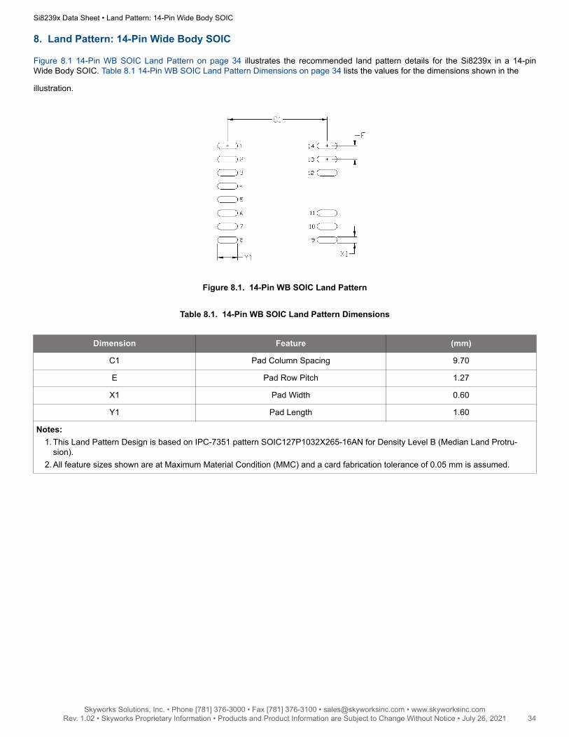
8. Land Pattern: 14-Pin Wide Body SOIC
Figure 8.1 14-Pin WB SOIC Land Pattern on page 34 illustrates the recommended land pattern details for the Si8239x in a 14-pinWide Body SOIC. Table 8.1 14-Pin WB SOIC Land Pattern Dimensions on page 34 lists the values for the dimensions shown in the
illustration.
Figure 8.1. 14-Pin WB SOIC Land Pattern
Table 8.1. 14-Pin WB SOIC Land Pattern Dimensions
Dimension Feature (mm)
C1 Pad Column Spacing 9.70
E Pad Row Pitch 1.27
X1 Pad Width 0.60
Y1 Pad Length 1.60
Notes:1. This Land Pattern Design is based on IPC-7351 pattern SOIC127P1032X265-16AN for Density Level B (Median Land Protru-
sion).2. All feature sizes shown are at Maximum Material Condition (MMC) and a card fabrication tolerance of 0.05 mm is assumed.
Si8239x Data Sheet • Land Pattern: 14-Pin Wide Body SOIC
Skyworks Solutions, Inc. • Phone [781] 376-3000 • Fax [781] 376-3100 • [email protected] • www.skyworksinc.com34 Rev. 1.02 • Skyworks Proprietary Information • Products and Product Information are Subject to Change Without Notice • July 26, 2021 34
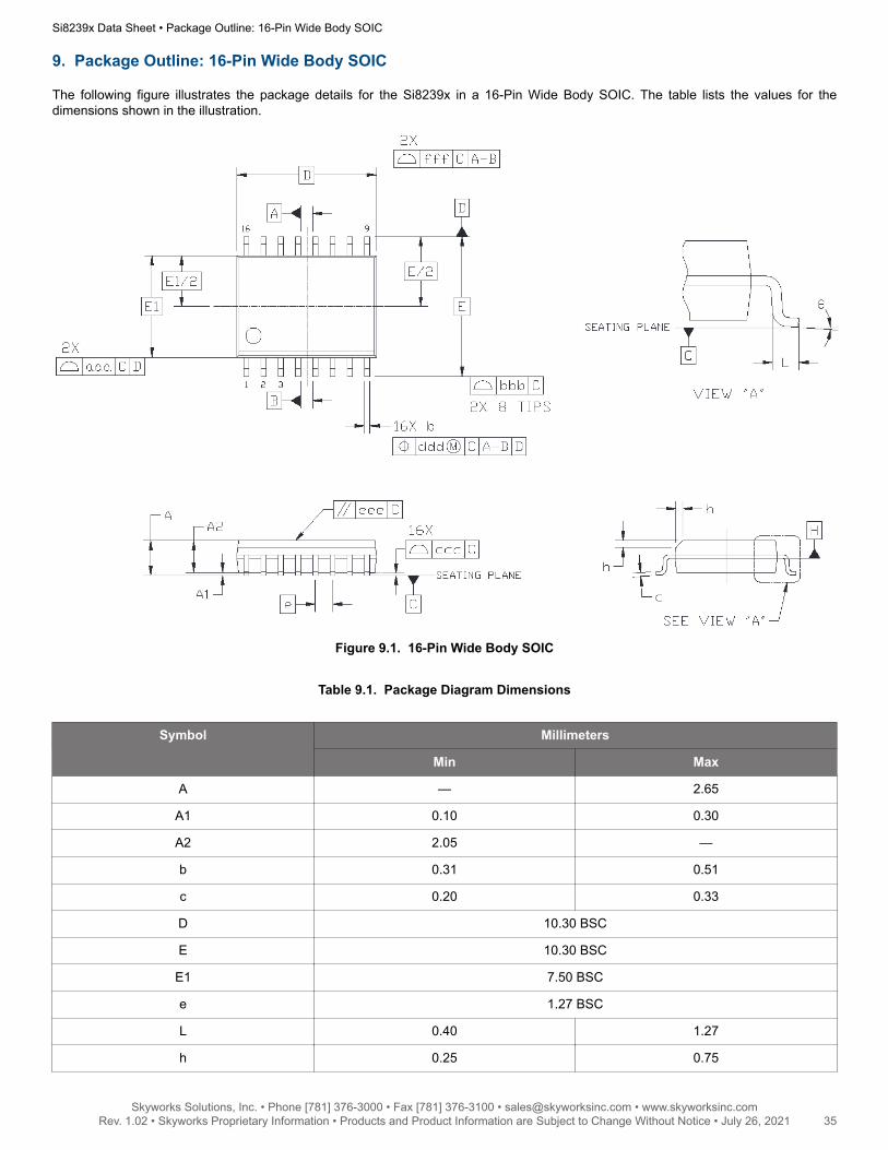
9. Package Outline: 16-Pin Wide Body SOIC
The following figure illustrates the package details for the Si8239x in a 16-Pin Wide Body SOIC. The table lists the values for thedimensions shown in the illustration.
Figure 9.1. 16-Pin Wide Body SOIC
Table 9.1. Package Diagram Dimensions
Symbol Millimeters
Min Max
A — 2.65
A1 0.10 0.30
A2 2.05 —
b 0.31 0.51
c 0.20 0.33
D 10.30 BSC
E 10.30 BSC
E1 7.50 BSC
e 1.27 BSC
L 0.40 1.27
h 0.25 0.75
Si8239x Data Sheet • Package Outline: 16-Pin Wide Body SOIC
Skyworks Solutions, Inc. • Phone [781] 376-3000 • Fax [781] 376-3100 • [email protected] • www.skyworksinc.com35 Rev. 1.02 • Skyworks Proprietary Information • Products and Product Information are Subject to Change Without Notice • July 26, 2021 35

Symbol Millimeters
Min Max
θ 0° 8°
aaa — 0.10
bbb — 0.33
ccc — 0.10
ddd — 0.25
eee — 0.10
fff — 0.20
Note:1. All dimensions shown are in millimeters (mm) unless otherwise noted.2. Dimensioning and Tolerancing per ANSI Y14.5M-1994.3. This drawing conforms to JEDEC Outline MS-013, Variation AA.4. Recommended reflow profile per JEDEC J-STD-020 specification for small body, lead-free components.
Si8239x Data Sheet • Package Outline: 16-Pin Wide Body SOIC
Skyworks Solutions, Inc. • Phone [781] 376-3000 • Fax [781] 376-3100 • [email protected] • www.skyworksinc.com36 Rev. 1.02 • Skyworks Proprietary Information • Products and Product Information are Subject to Change Without Notice • July 26, 2021 36
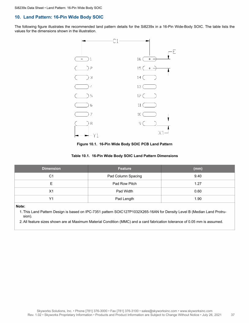
10. Land Pattern: 16-Pin Wide Body SOIC
The following figure illustrates the recommended land pattern details for the Si8239x in a 16-Pin Wide-Body SOIC. The table lists thevalues for the dimensions shown in the illustration.
Figure 10.1. 16-Pin Wide Body SOIC PCB Land Pattern
Table 10.1. 16-Pin Wide Body SOIC Land Pattern Dimensions
Dimension Feature (mm)
C1 Pad Column Spacing 9.40
E Pad Row Pitch 1.27
X1 Pad Width 0.60
Y1 Pad Length 1.90
Note:1. This Land Pattern Design is based on IPC-7351 pattern SOIC127P1032X265-16AN for Density Level B (Median Land Protru-
sion).2. All feature sizes shown are at Maximum Material Condition (MMC) and a card fabrication tolerance of 0.05 mm is assumed.
Si8239x Data Sheet • Land Pattern: 16-Pin Wide Body SOIC
Skyworks Solutions, Inc. • Phone [781] 376-3000 • Fax [781] 376-3100 • [email protected] • www.skyworksinc.com37 Rev. 1.02 • Skyworks Proprietary Information • Products and Product Information are Subject to Change Without Notice • July 26, 2021 37

11. Package Outline: 16-Pin Narrow Body SOIC
The following figure illustrates the package details for the Si8239x in a 16-Pin Narrow-Body SOIC. The table lists the values for thedimensions shown in the illustration.
Figure 11.1. 16-Pin Narrow Body SOIC
Table 11.1. Package Diagram Dimensions
Dimension Min Max Dimension Min Max
A — 1.75 L 0.40 1.27
A1 0.10 0.25 L2 0.25 BSC
A2 1.25 — h 0.25 0.50
b 0.31 0.51 θ 0° 8°
c 0.17 0.25 aaa 0.10
D 9.90 BSC bbb 0.20
E 6.00 BSC ccc 0.10
E1 3.90 BSC ddd 0.25
e 1.27 BSC
Note:1. All dimensions shown are in millimeters (mm) unless otherwise noted.2. Dimensioning and Tolerancing per ANSI Y14.5M-1994.3. This drawing conforms to the JEDEC Solid State Outline MS-012, Variation AC.4. Recommended card reflow profile is per the JEDEC/IPC J-STD-020 specification for Small Body Components.
Si8239x Data Sheet • Package Outline: 16-Pin Narrow Body SOIC
Skyworks Solutions, Inc. • Phone [781] 376-3000 • Fax [781] 376-3100 • [email protected] • www.skyworksinc.com38 Rev. 1.02 • Skyworks Proprietary Information • Products and Product Information are Subject to Change Without Notice • July 26, 2021 38
12. Land Pattern: 16-Pin Narrow Body SOIC
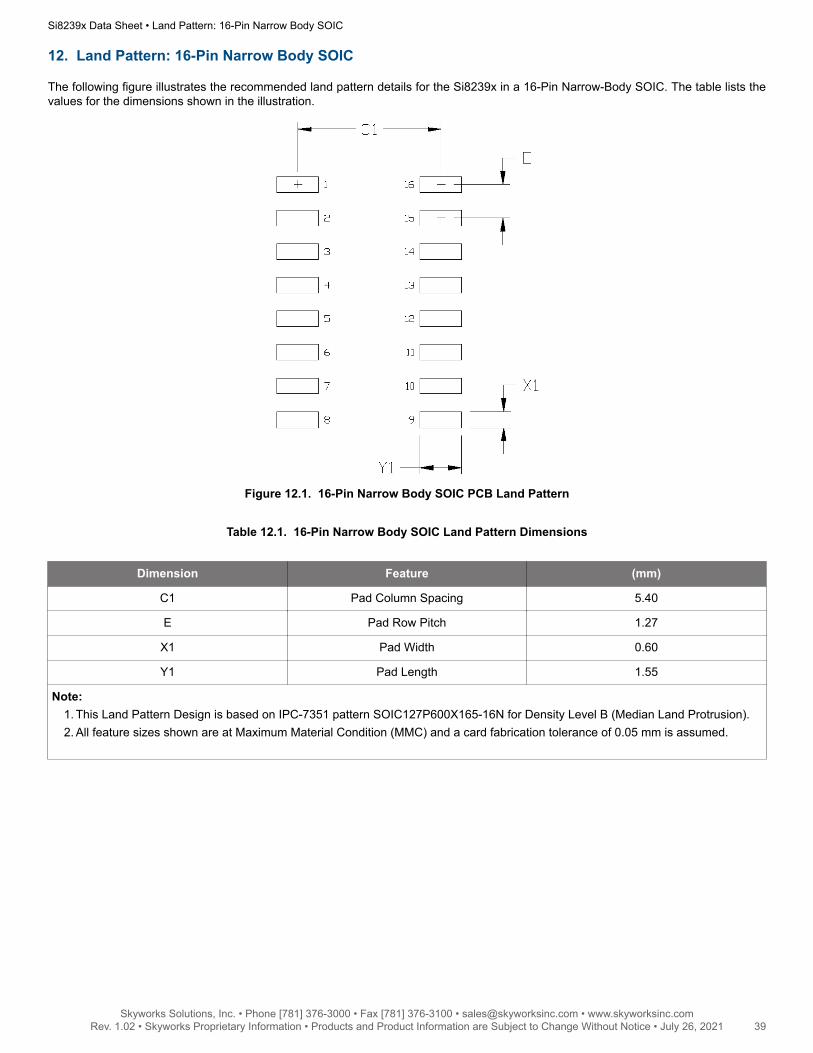
The following figure illustrates the recommended land pattern details for the Si8239x in a 16-Pin Narrow-Body SOIC. The table lists thevalues for the dimensions shown in the illustration.
Figure 12.1. 16-Pin Narrow Body SOIC PCB Land Pattern
Table 12.1. 16-Pin Narrow Body SOIC Land Pattern Dimensions
Dimension Feature (mm)
C1 Pad Column Spacing 5.40
E Pad Row Pitch 1.27
X1 Pad Width 0.60
Y1 Pad Length 1.55
Note:1. This Land Pattern Design is based on IPC-7351 pattern SOIC127P600X165-16N for Density Level B (Median Land Protrusion).2. All feature sizes shown are at Maximum Material Condition (MMC) and a card fabrication tolerance of 0.05 mm is assumed.
Si8239x Data Sheet • Land Pattern: 16-Pin Narrow Body SOIC
Skyworks Solutions, Inc. • Phone [781] 376-3000 • Fax [781] 376-3100 • [email protected] • www.skyworksinc.com39 Rev. 1.02 • Skyworks Proprietary Information • Products and Product Information are Subject to Change Without Notice • July 26, 2021 39

13. Top Markings
13.1 Si8239x Top Marking (14-/16-Pin Wide Body SOIC)
13.2 Top Marking Explanation (16-Pin Wide Body SOIC)
Line 1 Marking: Base Part Number
Ordering Options
See Ordering Guide for more informa-tion.
Si8239 = ISOdriver product series
Y = Output configuration: 0, 1, 3, 4, 5, 6, 7, 8
0, 1, 5, 6, 7 = Dual drivers
3 = Dual input (VIA, VIB) High Side/Low Side drivers
4, 8 = PWM input High side/Low side drivers
U = UVLO level: A, B, C
A = 6 V; B = 8 V; C = 12 V
V = Isolation rating: B, D
B = 2.5 kV; D = 5.0 kV
D = Dead time setting range: none, 4
none = 10–200 ns; 4 = 40–600 ns
Line 2 Marking: YY = Year
WW = Workweek
Assigned by the Assembly House. Corresponds to the yearand workweek of the mold date.
TTTTTT = Mfg Code Manufacturing Code from Assembly Purchase Order form.
Line 3 Marking: Circle = 1.5 mm Diameter
(Center Justified)
“e4” Pb-Free Symbol
Country of Origin
ISO Code Abbreviation
TW = Taiwan
Si8239x Data Sheet • Top Markings
Skyworks Solutions, Inc. • Phone [781] 376-3000 • Fax [781] 376-3100 • [email protected] • www.skyworksinc.com40 Rev. 1.02 • Skyworks Proprietary Information • Products and Product Information are Subject to Change Without Notice • July 26, 2021 40
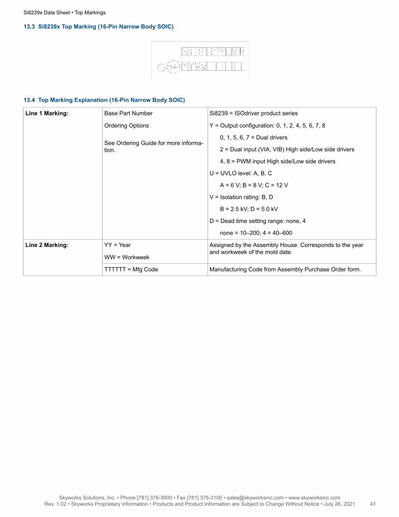
13.3 Si8239x Top Marking (16-Pin Narrow Body SOIC)
13.4 Top Marking Explanation (16-Pin Narrow Body SOIC)
Line 1 Marking: Base Part Number
Ordering Options
See Ordering Guide for more informa-tion.
Si8239 = ISOdriver product series
Y = Output configuration: 0, 1, 2, 4, 5, 6, 7, 8
0, 1, 5, 6, 7 = Dual drivers
2 = Dual input (VIA, VIB) High side/Low side drivers
4, 8 = PWM input High side/Low side drivers
U = UVLO level: A, B, C
A = 6 V; B = 8 V; C = 12 V
V = Isolation rating: B, D
B = 2.5 kV; D = 5.0 kV
D = Dead time setting range: none, 4
none = 10–200; 4 = 40–600
Line 2 Marking: YY = Year
WW = Workweek
Assigned by the Assembly House. Corresponds to the yearand workweek of the mold date.
TTTTTT = Mfg Code Manufacturing Code from Assembly Purchase Order form.
Si8239x Data Sheet • Top Markings
Skyworks Solutions, Inc. • Phone [781] 376-3000 • Fax [781] 376-3100 • [email protected] • www.skyworksinc.com41 Rev. 1.02 • Skyworks Proprietary Information • Products and Product Information are Subject to Change Without Notice • July 26, 2021 41
14. Revision History
Revision 1.02
August 2020• Added new package• Corresponding -A OPNs are added for all existing -I OPNs• Safety and certification tables were brought up-to-date• Power calculation section updated• Application diagrams updated to clarify devices represented• Enhanced UVLO description taken to separate section• Output threshold specs added for digital output pin
Revision 1.01
July 2018• Added Automotive-grade information including features, applications, and Ordering Guide table.
Si8239x Data Sheet • Revision History
Skyworks Solutions, Inc. • Phone [781] 376-3000 • Fax [781] 376-3100 • [email protected] • www.skyworksinc.com42 Rev. 1.02 • Skyworks Proprietary Information • Products and Product Information are Subject to Change Without Notice • July 26, 2021 42

Copyright © 2021 Skyworks Solutions, Inc. All Rights Reserved.Information in this document is provided in connection with Skyworks Solutions, Inc. (“Skyworks”) products or services. These materials, including the information contained herein, are provided by Skyworks as a service to its customers and may be used for informational purposes only by the customer. Skyworks assumes no responsibility for errors or omissions in these materials or the information contained herein. Skyworks may change its documentation, products, services, specifications or product descriptions at any time, without notice. Skyworks makes no commitment to update the materials or information and shall have no responsibility whatsoever for conflicts, incompatibilities, or other difficulties arising from any future changes.
No license, whether express, implied, by estoppel or otherwise, is granted to any intellectual property rights by this document. Skyworks assumes no liability for any materials, products or information provided hereunder, including the sale, distribution, reproduction or use of Skyworks products, information or materials, except as may be provided in Skyworks’ Terms and Conditions of Sale.
THE MATERIALS, PRODUCTS AND INFORMATION ARE PROVIDED “AS IS” WITHOUT WARRANTY OF ANY KIND, WHETHER EXPRESS, IMPLIED, STATUTORY, OR OTHERWISE, INCLUDING FITNESS FOR A PARTICULAR PURPOSE OR USE, MERCHANTABILITY, PERFORMANCE, QUALITY OR NON-INFRINGEMENT OF ANY INTELLECTUAL PROPERTY RIGHT; ALL SUCH WARRANTIES ARE HEREBY EXPRESSLY DISCLAIMED. SKYWORKS DOES NOT WARRANT THE ACCURACY OR COMPLETENESS OF THE INFORMATION, TEXT, GRAPHICS OR OTHER ITEMS CONTAINED WITHIN THESE MATERIALS. SKYWORKS SHALL NOT BE LIABLE FOR ANY DAMAGES, INCLUDING BUT NOT LIMITED TO ANY SPECIAL, INDIRECT, INCIDENTAL, STATUTORY, OR CONSEQUENTIAL DAMAGES, INCLUDING WITHOUT LIMITATION, LOST REVENUES OR LOST PROFITS THAT MAY RESULT FROM THE USE OF THE MATERIALS OR INFORMATION, WHETHER OR NOT THE RECIPIENT OF MATERIALS HAS BEEN ADVISED OF THE POSSIBILITY OF SUCH DAMAGE.
Skyworks products are not intended for use in medical, lifesaving or life-sustaining applications, or other equipment in which the failure of the Skyworks products could lead to personal injury, death, physical or environmental damage. Skyworks customers using or selling Skyworks products for use in such applications do so at their own risk and agree to fully indemnify Skyworks for any damages resulting from such improper use or sale.
Customers are responsible for their products and applications using Skyworks products, which may deviate from published specifications as a result of design defects, errors, or operation of products outside of published parameters or design specifications. Customers should include design and operating safeguards to minimize these and other risks. Skyworks assumes no liability for applications assistance, customer product design, or damage to any equipment resulting from the use of Skyworks products outside of Skyworks’ published specifications or parameters.
Skyworks, the Skyworks symbol, Sky5®, SkyOne®, SkyBlue™, Skyworks Green™, Clockbuilder®, DSPLL®, ISOmodem®, ProSLIC®, and SiPHY® are trademarks or registered trademarks of Skyworks Solutions, Inc. or its subsidiaries in the United States and other countries. Third-party brands and names are for identification purposes only and are the property of their respective owners. Additional information, including relevant terms and conditions, posted at www.skyworksinc.com, are incorporated by reference.
Portfoliowww.skyworksinc.com
Qualitywww.skyworksinc.com/quality
Support & Resourceswww.skyworksinc.com/support
Connecting Everyone
and Everything,
All the Time
Skyworks Solutions, Inc. | Nasdaq: SWKS | [email protected] | www.skyworksinc.comUSA: 781-376-3000 | Asia: 886-2-2735 0399 | Europe: 33 (0)1 43548540 |