Embed Size (px)
Citation preview
Programmable Frequency Scan Waveform Generator
Data Sheet AD5932
Rev. A Information furnished by Analog Devices is believed to be accurate and reliable. However, no responsibility is assumed by Analog Devices for its use, nor for any infringements of patents or other rights of third parties that may result from its use. Specifications subject to change without notice. No license is granted by implication or otherwise under any patent or patent rights of Analog Devices. Trademarks and registered trademarks are the property of their respective owners.
One Technology Way, P.O. Box 9106, Norwood, MA 02062-9106, U.S.A. Tel: 781.329.4700 www.analog.com Fax: 781.461.3113 ©2006–2012 Analog Devices, Inc. All rights reserved.
FEATURES Programmable frequency profile
No external components necessary Output frequency up to 25 MHz Burst-and-listen capability Preprogrammable frequency profile minimizes number of
DSP/microcontroller writes Sinusoidal/triangular/square wave outputs Automatic or single pin control of frequency stepping Power-down mode: 20 µA Power supply: 2.3 V to 5.5 V Automotive temperature range: −40°C to +125°C 16-lead, Pb-free TSSOP
APPLICATIONS Frequency scanning/radar Network/impedance measurements Incremental frequency stimulus Sensory applications
Proximity and motion
GENERAL DESCRIPTION
The AD59321 is a waveform generator offering a programmable frequency scan. Utilizing embedded digital processing that allows enhanced frequency control, the device generates synthesized analog or digital frequency-stepped waveforms. Because frequency profiles are preprogrammed, continuous write cycles are eliminated, thereby freeing up valuable DSP/microcontroller resources. Waveforms start from a known phase and are incremented phase-continuously, which allows phase shifts to be easily determined. Consuming only 6.7 mA, the AD5932 provides a convenient low power solution to waveform generation.
The AD5932 outputs each frequency in the range of interest for a defined length of time and then steps to the next frequency in the scan range. The length of time the device outputs a particular frequency is preprogrammed, and the device increments the frequency automatically; or, alternatively, the frequency is incremented externally via the CTRL pin. At the end of the range, the AD5932 continues to output the last frequency until the device is reset. The AD5932 also offers a digital output via the MSBOUT pin.
(continued on Page 3)
FUNCTIONAL BLOCK DIAGRAM
AD5932
DVDD CAP/2.5V DGND INTERRUPT STANDBY AGND AVDD
VCC2.5V
SYNCMCLK
CTRL
FSYNC
SYNCOUT
MSBOUT
VOUT
COMP
SCLK SDATA
DATA AND CONTROL
FREQUENCYCONTROLLER
INCREMENTCONTROLLER
CONTROLREGISTER
ON-BOARDREFERENCE
FULL-SCALECONTROL
24-BITPIPELINEDDDS CORE 10-BIT
DAC
SERIAL INTERFACE
REGULATOR
DATA INCR
BUFFER
BUFFER
/24
0541
6-00
1
Figure 1.
1 Protected by U.S. patent number 6747583.
AD5932* Product Page Quick LinksLast Content Update: 08/30/2016
Comparable PartsView a parametric search of comparable parts
Evaluation Kits• AD5932 Evaluation Board
DocumentationApplication Notes• AN-1044: Programming the AD5932 for Frequency Sweep
and Single Frequency Outputs• AN-1248: SPI Interface• AN-1389: Recommended Rework Procedure for the Lead
Frame Chip Scale Package (LFCSP)• AN-237: Choosing DACs for Direct Digital Synthesis• AN-280: Mixed Signal Circuit Technologies• AN-342: Analog Signal-Handling for High Speed and
Accuracy• AN-345: Grounding for Low-and-High-Frequency Circuits• AN-419: A Discrete, Low Phase Noise, 125 MHz Crystal
Oscillator for the AD9850• AN-423: Amplitude Modulation of the AD9850 Direct
Digital Synthesizer• AN-543: High Quality, All-Digital RF Frequency
Modulation Generation with the ADSP-2181 and the AD9850 DDS
• AN-557: An Experimenter's Project:• AN-587: Synchronizing Multiple AD9850/AD9851 DDS-
Based Synthesizers• AN-605: Synchronizing Multiple AD9852 DDS-Based
Synthesizers• AN-621: Programming the AD9832/AD9835• AN-632: Provisionary Data Rates Using the AD9951 DDS
as an Agile Reference Clock for the ADN2812 Continuous-Rate CDR
• AN-769: Generating Multiple Clock Outputs from the AD9540
• AN-772: A Design and Manufacturing Guide for the Lead Frame Chip Scale Package (LFCSP)
• AN-823: Direct Digital Synthesizers in Clocking Applications Time
• AN-837: DDS-Based Clock Jitter Performance vs. DAC Reconstruction Filter Performance
• AN-843: Measuring a Loudspeaker Impedance Profile Using the AD5933
• AN-847: Measuring a Grounded Impedance Profile Using the AD5933
• AN-851: A WiMax Double Downconversion IF Sampling Receiver Design
• AN-927: Determining if a Spur is Related to the DDS/DAC or to Some Other Source (For Example, Switching Supplies)
• AN-939: Super-Nyquist Operation of the AD9912 Yields a High RF Output Signal
• AN-953: Direct Digital Synthesis (DDS) with a Programmable Modulus
Data Sheet• AD5932: Programmable Frequency Scan Waveform
Generator Data SheetProduct Highlight• Introducing Digital Up/Down Converters: VersaCOMM™
Reconfigurable Digital ConvertersUser Guides• UG-796: Evaluation Board for Programmable Single-Scan
Waveform Generator
Software and Systems Requirements• AD5932 Evaluation Software
Tools and Simulations• ADIsimDDS (Direct Digital Synthesis) - BETA
Reference MaterialsTechnical Articles• 400-MSample DDSs Run On Only +1.8 VDC• ADI Buys Korean Mobile TV Chip Maker• Basics of Designing a Digital Radio Receiver (Radio 101)• Clock Requirements For Data Converters• DDS Applications• DDS Circuit Generates Precise PWM Waveforms• DDS Design• DDS Device Produces Sawtooth Waveform• DDS Device Provides Amplitude Modulation• DDS IC Initiates Synchronized Signals• DDS IC Plus Frequency-To-Voltage Converter Make Low-
Cost DAC• DDS Simplifies Polar Modulation• Digital Potentiometers Vary Amplitude In DDS Devices• Digital Up/Down Converters: VersaCOMM™ White Paper• Digital Waveform Generator Provides Flexible Frequency
Tuning for Sensor Measurement• Improved DDS Devices Enable Advanced Comm Systems• Integrated DDS Chip Takes Steps To 2.7 GHz• Simple Circuit Controls Stepper Motors• Speedy A/Ds Demand Stable Clocks• Synchronized Synthesizers Aid Multichannel Systems• The Year of the Waveform Generator• Two DDS ICs Implement Amplitude-shift Keying• Video Portables and Cameras Get HDMI Outputs
Design Resources• AD5932 Material Declaration• PCN-PDN Information• Quality And Reliability• Symbols and Footprints
DiscussionsView all AD5932 EngineerZone Discussions
Sample and BuyVisit the product page to see pricing options
Technical SupportSubmit a technical question or find your regional support number
* This page was dynamically generated by Analog Devices, Inc. and inserted into this data sheet. Note: Dynamic changes to the content on this page does not constitute a change to the revision number of the product data sheet. This content may be frequently modified.
AD5932 Data Sheet
Rev. A | Page 2 of 28
TABLE OF CONTENTS Features .............................................................................................. 1
Applications ....................................................................................... 1
General Description ......................................................................... 1
Functional Block Diagram .............................................................. 1
Revision History ............................................................................... 2
Specifications ..................................................................................... 4
Specifications Test Circuit ........................................................... 5
Timing Specifications .................................................................. 6
Master Clock and Timing Diagrams ......................................... 6
Absolute Maximum Ratings ............................................................ 8
ESD Caution .................................................................................. 8
Pin Configuration and Function Descriptions ............................. 9
Typical Performance Characteristics ........................................... 10
Terminology .................................................................................... 14
Theory of Operation ...................................................................... 15
Frequency Profile........................................................................ 15
Serial Interface ............................................................................ 15
Powering up the AD5932 .......................................................... 15
Programming the AD5932 ........................................................ 16
Setting Up the Frequency Scan................................................. 17
Activating and Controlling the Scan ....................................... 18
Outputs from the AD5932 ........................................................ 19
Applications ..................................................................................... 20
Grounding and Layout .............................................................. 20
AD5932 to ADSP-21xx Interface ............................................. 20
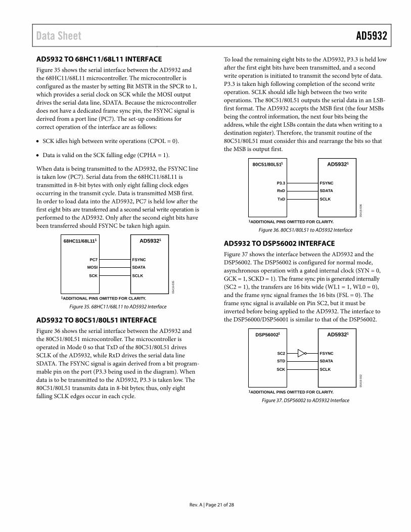
AD5932 to 68HC11/68L11 Interface ....................................... 21
AD5932 to 80C51/80L51 Interface .......................................... 21
AD5932 to DSP56002 Interface ............................................... 21
Evaluation Board ............................................................................ 22
Schematics ................................................................................... 23
Outline Dimensions ....................................................................... 25
Ordering Guide .......................................................................... 25
REVISION HISTORY
2/12—Rev. 0 to Rev. A Changes to Figure 21, Figure 22, Figure 23, Figure 24, and Figure 25 .......................................................................................... 12 Changes to Figure 26, Figure 27, Figure 28, and Figure 29 ....... 13
4/06—Revision 0: Initial Version
Data Sheet AD5932
Rev. A | Page 3 of 28
GENERAL DESCRIPTION (continued from Page 1)
To program the AD5932, the user enters the start frequency, the increment step size, the number of increments to be made, and the time interval that the part outputs each frequency. The fre-quency scan profile is initiated, started, and executed by toggling the CTRL pin.
The AD5932 is written to via a 3-wire serial interface that operates at clock rates up to 40 MHz. The device operates with a power supply from 2.3 V to 5.5 V.
Note that the AVDD and DVDD are independent of each other and can be operated from different voltages. The AD5932 also has a standby function that allows sections of the device that are not in use to be powered down.
The AD5932 is available in a 16-lead, Pb-free TSSOP.
AD5932 Data Sheet
Rev. A | Page 4 of 28
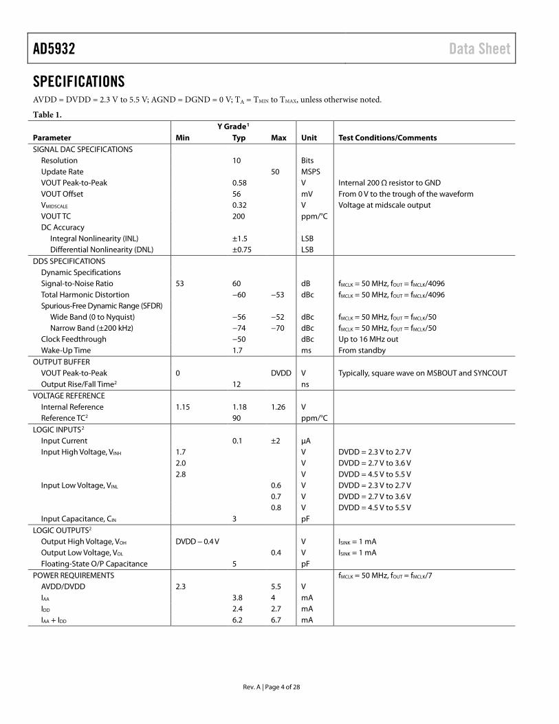
SPECIFICATIONS AVDD = DVDD = 2.3 V to 5.5 V; AGND = DGND = 0 V; TA = TMIN to TMAX, unless otherwise noted.
Table 1. Y Grade1 Parameter Min Typ Max Unit Test Conditions/Comments SIGNAL DAC SPECIFICATIONS
Resolution 10 Bits Update Rate 50 MSPS VOUT Peak-to-Peak 0.58 V Internal 200 Ω resistor to GND VOUT Offset 56 mV From 0 V to the trough of the waveform VMIDSCALE 0.32 V Voltage at midscale output VOUT TC 200 ppm/°C DC Accuracy
Integral Nonlinearity (INL) ±1.5 LSB Differential Nonlinearity (DNL) ±0.75 LSB
DDS SPECIFICATIONS Dynamic Specifications Signal-to-Noise Ratio 53 60 dB fMCLK = 50 MHz, fOUT = fMCLK/4096 Total Harmonic Distortion −60 −53 dBc fMCLK = 50 MHz, fOUT = fMCLK/4096 Spurious-Free Dynamic Range (SFDR)
Wide Band (0 to Nyquist) −56 −52 dBc fMCLK = 50 MHz, fOUT = fMCLK/50 Narrow Band (±200 kHz) −74 −70 dBc fMCLK = 50 MHz, fOUT = fMCLK/50
Clock Feedthrough −50 dBc Up to 16 MHz out Wake-Up Time 1.7 ms From standby
OUTPUT BUFFER VOUT Peak-to-Peak 0 DVDD V Typically, square wave on MSBOUT and SYNCOUT Output Rise/Fall Time2 12 ns
VOLTAGE REFERENCE Internal Reference 1.15 1.18 1.26 V Reference TC2 90 ppm/°C
LOGIC INPUTS2 Input Current 0.1 ±2 µA Input High Voltage, VINH 1.7 V DVDD = 2.3 V to 2.7 V 2.0 V DVDD = 2.7 V to 3.6 V 2.8 V DVDD = 4.5 V to 5.5 V Input Low Voltage, VINL 0.6 V DVDD = 2.3 V to 2.7 V 0.7 V DVDD = 2.7 V to 3.6 V 0.8 V DVDD = 4.5 V to 5.5 V Input Capacitance, CIN 3 pF
LOGIC OUTPUTS2 Output High Voltage, VOH DVDD − 0.4 V V ISINK = 1 mA Output Low Voltage, VOL 0.4 V ISINK = 1 mA Floating-State O/P Capacitance 5 pF
POWER REQUIREMENTS fMCLK = 50 MHz, fOUT = fMCLK/7 AVDD/DVDD 2.3 5.5 V IAA 3.8 4 mA IDD 2.4 2.7 mA IAA + IDD 6.2 6.7 mA

Data Sheet AD5932
Rev. A | Page 5 of 28
Y Grade1 Parameter Min Typ Max Unit Test Conditions/Comments
Low Power Sleep Mode Device is reset before putting into standby 20 85 µA All outputs powered down, MCLK = 0 V,
serial interface active 140 240 µA All outputs powered down, MCLK active,
serial interface active 1 Operating temperature range is as follows: Y version: −40°C to +125°C; typical specifications are at +25°C. 2 Guaranteed by design, not production tested.
SPECIFICATIONS TEST CIRCUIT
10-BITDAC
SINROM
AVDD
REGULATOR
20pF
10nF
COMP
VOUT
AD5932
CAP/2.5V
12
100nF 10nF
0541
6-00
2
Figure 2. Test Circuit Used to Test the Specifications

AD5932 Data Sheet
Rev. A | Page 6 of 28
TIMING SPECIFICATIONS All input signals are specified with tR = tF = 5 ns (10% to 90% of VDD) and are timed from a voltage level of (VIL + VIH)/2 (see Figure 3 to Figure 6). DVDD = 2.3 V to 5.5 V; AGND = DGND = 0 V; all specifications TMIN to TMAX, unless otherwise noted.
Table 2. Parameter1 Limit at TMIN, TMAX Unit Conditions/Comments t1 20 ns min MCLK period t2 8 ns min MCLK high duration t3 8 ns min MCLK low duration t4 25 ns min SCLK period t5 10 ns min SCLK high time t6 10 ns min SCLK low time t7 5 ns min FSYNC to SCLK falling edge setup time t8 10 ns min FSYNC to SCLK hold time t9 5 ns min Data setup time t10 3 ns min Data hold time t11 2 × t1 ns min Minimum CTRL pulse width t12 0 ns min CTRL rising edge to MCLK falling edge setup time t13 10 × t1 ns typ CTRL rising edge to VOUT delay (initial pulse, includes initialization) 8 × t1 ns typ CTRL rising edge to VOUT delay (initial pulse, includes initialization) t14 1 × t1 ns typ Frequency change to SYNC output, each frequency increment t15 2 × t1 ns typ Frequency change to SYNC output, end of scan t16 20 ns max MCLK falling edge to MSBOUT 1 Guaranteed by design, not production tested.
MASTER CLOCK AND TIMING DIAGRAMS
MCLK
t3
t2
t1
0541
6-00
3
Figure 3. Master Clock
SCLK
FSYNC
SDATA D15 D14 D2 D1 D0 D15 D14
t7
t9
t6 t8
t10
t5 t4
0541
6-00
4
Figure 4. Serial Timing

Data Sheet AD5932
Rev. A | Page 7 of 28
MCLK
CTRL
VOUT
t12
t11
t13
0541
6-00
5
Figure 5. CTRL Timing
CTRL
VOUT
SYNCOUT(Each Frequency
Increment)
SYNCOUT(End of Scan)
t13
t15
t14
0541
6-00
6
Figure 6. SYNCOUT Timing

AD5932 Data Sheet
Rev. A | Page 8 of 28
ABSOLUTE MAXIMUM RATINGS TA = 25°C, unless otherwise noted.
Table 3. Parameter Rating AVDD to AGND −0.3 V to +6.0 V DVDD to DGND −0.3 V to +6.0 V AGND to DGND −0.3 V to +0.3 V CAP/2.5 V to DGND −0.3 V to +2.75 V Digital I/O Voltage to DGND −0.3 V to DVDD + 0.3 V Analog I/O Voltage to AGND −0.3 V to AVDD + 0.3 V Operating Temperature Range Automotive (Y Version) −40°C to +125°C Storage Temperature Range −65°C to +150°C Maximum Junction Temperature +150°C TSSOP (4-Layer Board)
θJA Thermal Impedance 112°C/W θJC Thermal Impedance 27.6°C/W
Reflow Soldering (Pb-Free) 300°C Peak Temperature 260(+0/−5)°C Time at Peak Temperature 10 sec to 40 sec
Stresses above those listed under Absolute Maximum Ratings may cause permanent damage to the device. This is a stress rating only; functional operation of the device at these or any other conditions above those indicated in the operational section of this specification is not implied. Exposure to absolute maximum rating conditions for extended periods may affect device reliability.
ESD CAUTION ESD (electrostatic discharge) sensitive device. Electrostatic charges as high as 4000 V readily accumulate on the human body and test equipment and can discharge without detection. Although this product features proprietary ESD protection circuitry, permanent damage may occur on devices subjected to high energy electrostatic discharges. Therefore, proper ESD precautions are recommended to avoid performance degradation or loss of functionality.

Data Sheet AD5932
Rev. A | Page 9 of 28
PIN CONFIGURATION AND FUNCTION DESCRIPTIONS
0541
6-00
7
TOP VIEW(Not to Scale)
1
2
3
4
5
6
7
8
AD5932
16
15
14
13
12
11
10
9
AVDD
DVDD
CAP/2.5V
SYNCOUT
MCLK
DGND
COMP
AGND
STANDBY
FSYNC
CTRL
MSBOUT INTERRUPT
SDATA
SCLK
VOUT
Figure 7. Pin Configuration
Table 4. Pin Function Descriptions Pin No. Mnemonic Description 1 COMP DAC Bias Pin. This pin is used for decoupling the DAC bias voltage to AVDD. 2 AVDD Positive Power Supply for the Analog Section. AVDD can have a value from 2.3 V to 5.5 V. A 0.1 µF decoupling
capacitor should be connected between AVDD and AGND. 3 DVDD Positive Power Supply for the Digital Section. DVDD can have a value from 2.3 V to 5.5 V. A 0.1 µF decoupling
capacitor should be connected between DVDD and DGND. 4 CAP/2.5V Digital Circuitry. Operates from a 2.5 V power supply. This 2.5 V is generated from DVDD using an on-board
regulator. The regulator requires a decoupling capacitor of typically 100 nF, which is connected from CAP/2.5V to DGND. If DVDD is equal to or less than 2.7 V, CAP/2.5V can be shorted to DVDD.
5 DGND Ground for All Digital Circuitry. 6 MCLK Digital Clock Input. DDS output frequencies are expressed as a binary fraction of the frequency of MCLK.
The output frequency accuracy and phase noise are determined by this clock. 7 SYNCOUT Digital Output for Scan Status Information. User-selectable for end of scan (EOS) or frequency increments through
the control register (SYNCOP bit). This pin must be enabled by setting the SYNCOUTEN bit in the control register to 1. 8 MSBOUT Digital Output. The inverted MSB of the DAC data is available at this pin. This output pin must be enabled by
setting the MSBOUTEN bit in the control register to 1. 9 INTERRUPT Digital Input. This pin acts as an interrupt during a frequency scan. A low-to-high transition is sampled by the
internal MCLK, which resets internal state machines. This results in the DAC output going to midscale. 10 CTRL Digital Input. Triple function pin for initialization, start, and external frequency increments. A low-to-high transition,
sampled by the internal MCLK, is used to initialize and start internal state machines, which then execute the pre-programmed frequency scan sequence. When in auto-increment mode, a single pulse executes the entire scan sequence. When in external increment mode, each frequency increment is triggered by low-to-high transitions.
11 SDATA Serial Data Input. The 16-bit serial data-word is applied to this input with the register address first, followed by the MSB to LSBs of the data.
12 SCLK Serial Clock Input. Data is clocked into the AD5932 on each falling SCLK edge. 13 FSYNC Active Low Control Input. This is the frame synchronization signal for the serial data. When FSYNC is taken low,
the internal logic is informed that a new word is being loaded into the device. 14 STANDBY Active High Digital Input. When this pin is high, the internal MCLK is disabled, and the reference DAC and regulator
are powered down. For optimum power saving, it is recommended that the AD5932 be reset before it is put into standby, as this results in a shutdown current of typically 20 µA.
15 AGND Ground for All Analog Circuitry. 16 VOUT Voltage Output. The analog outputs from the AD5932 are available here. An external resistive load is not required,
because the device has a 200 Ω resistor on board. A 20 pF capacitor to AGND is recommended to act as a low-pass filter and to reduce clock feedthrough.
AD5932 Data Sheet
Rev. A | Page 10 of 28
TYPICAL PERFORMANCE CHARACTERISTICS
MCLK FREQUENCY (MHz)
9
8
7
6
4
3
5
2
1
00 5045403530252015105
0541
6-00
8
I DD
(mA
)
TA = 25°CAVDD = 5VMSBOUT, SYNCOUT ENABLED
DVDD = 5V
DVDD = 5V, FOUT = MCLK/7
DVDD = 3V, FOUT = MCLK/7
DVDD = 3V
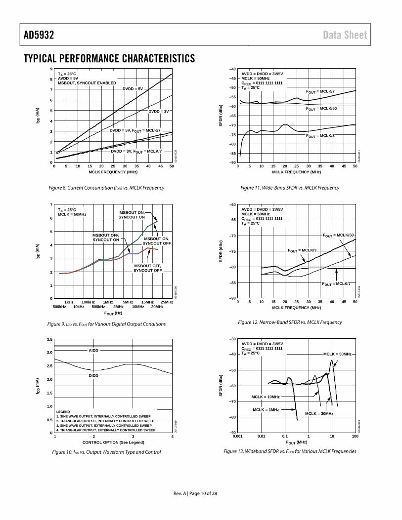
Figure 8. Current Consumption (IDD) vs. MCLK Frequency
FOUT (Hz)
7
6
4
3
5
2
1
025MHz
20MHz15MHz
10MHz5MHz
2MHz1MHz
500kHz100kHz
10kHz1kHz
500kHz
0541
6-00
9
I DD
(mA
)
TA = 25°CMCLK = 50MHz MSBOUT ON,
SYNCOUT ON
MSBOUT OFF,SYNCOUT OFF
MSBOUT ON,SYNCOUT OFF
MSBOUT OFF,SYNCOUT ON
Figure 9. IDD vs. FOUT for Various Digital Output Conditions
LEGEND1. SINE WAVE OUTPUT, INTERNALLY CONTROLLED SWEEP2. TRIANGULAR OUTPUT, INTERNALLY CONTROLLED SWEEP3. SINE WAVE OUTPUT, EXTERNALLY CONTROLLED SWEEP4. TRIANGULAR OUTPUT, EXTERNALLY CONTROLLED SWEEP
CONTROL OPTION (See Legend)
3.5
3.0
2.0
1.5
2.5
1.0
0.5
03 421
0541
6-01
0
I DD
(mA
)
AIDD
DIDD
Figure 10. IDD vs. Output Waveform Type and Control
MCLK FREQUENCY (MHz)
–40
–45
–50
–55
–60
–65
–70
–75
–80
–85
–900 5045403530252015105
0541
6-01
1
SFD
R (d
Bc)
AVDD = DVDD = 3V/5VMCLK = 50MHzCREG = 0111 1111 1111TA = 25°C
FOUT = MCLK/7
FOUT = MCLK/50
FOUT = MCLK/3
Figure 11. Wide-Band SFDR vs. MCLK Frequency
MCLK FREQUENCY (MHz)
–60
–65
–70
–75
–80
–85
–900 5045403530252015105
0541
6-01
2
SFD
R (d
Bc)
AVDD = DVDD = 3V/5VMCLK = 50MHzCREG = 0111 1111 1111TA = 25°C
FOUT = MCLK/7
FOUT = MCLK/50
FOUT = MCLK/3
Figure 12. Narrow-Band SFDR vs. MCLK Frequency
FOUT (MHz)
–30
–40
–50
–60
–70
–80
–900.001 1001010.10.01
0541
6-01
3
SFD
R (d
Bc)
AVDD = DVDD = 3V/5VCREG = 0111 1111 1111TA = 25°C
MCLK = 1MHz
MCLK = 10MHz
MCLK = 30MHz
MCLK = 50MHz
Figure 13. Wideband SFDR vs. FOUT for Various MCLK Frequencies
Data Sheet AD5932
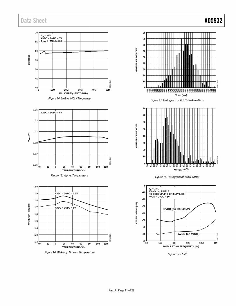
Rev. A | Page 11 of 28
MCLK FREQUENCY (MHz)
70
65
60
55
50
45
4050M40M30M20M10M0
0541
6-01
4
SNR
(dB
)
TA = 25°CAVDD = DVDD = 5VfOUT = FMCLK/4096
Figure 14. SNR vs. MCLK Frequency
TEMPERATURE (°C)
1.25
1.23
1.21
1.19
1.17
1.15120100806040200–40 –20
0541
6-01
5
V REF
(V)
AVDD = DVDD = 5V
Figure 15. VREF vs. Temperature
TEMPERATURE (°C)
2.0
1.8
1.9
1.7
1.6
1.5
1.3
1.4
1.2120100806040200–40 –20
0541
6-01
6
WA
KE-
UP
TIM
E (m
s)
AVDD = DVDD = 5V
AVDD = DVDD = 2.3V
Figure 16. Wake-up Time vs. Temperature
V p-p (mV)
0541
6-01
7
NU
MB
ER O
F D
EVIC
ES
0
10
20
30
40
50
60
70
80
90
565
566
567
568
569
570
571
572
573
574
575
576
577
578
579
580
581
582
583
584
585
586
587
588
589
590
591
592
593
594
595
596
597
Figure 17. Histogram of VOUT Peak-to-Peak
VOFFSET (mV)
80
70
60
50
40
30
10
20
0 0541
6-01
8
NU
MB
ER O
F D
EVIC
ES
706968676665646362616059585756555453525150
Figure 18. Histogram of VOUT Offset
MODULATING FREQUENCY (Hz)
0
–10
–20
–30
–40
–50
–70
–60
–8010 1M100k10k1k100
0541
6-01
9
ATT
ENU
ATI
ON
(dB
)
TA = 25°C100mV p-p RIPPLENO DECOUPLING ON SUPPLIESAVDD = DVDD = 5V
AVDD (on VOUT)
DVDD (on CAP/2.5V)
Figure 19. PSSR
AD5932 Data Sheet
Rev. A | Page 12 of 28
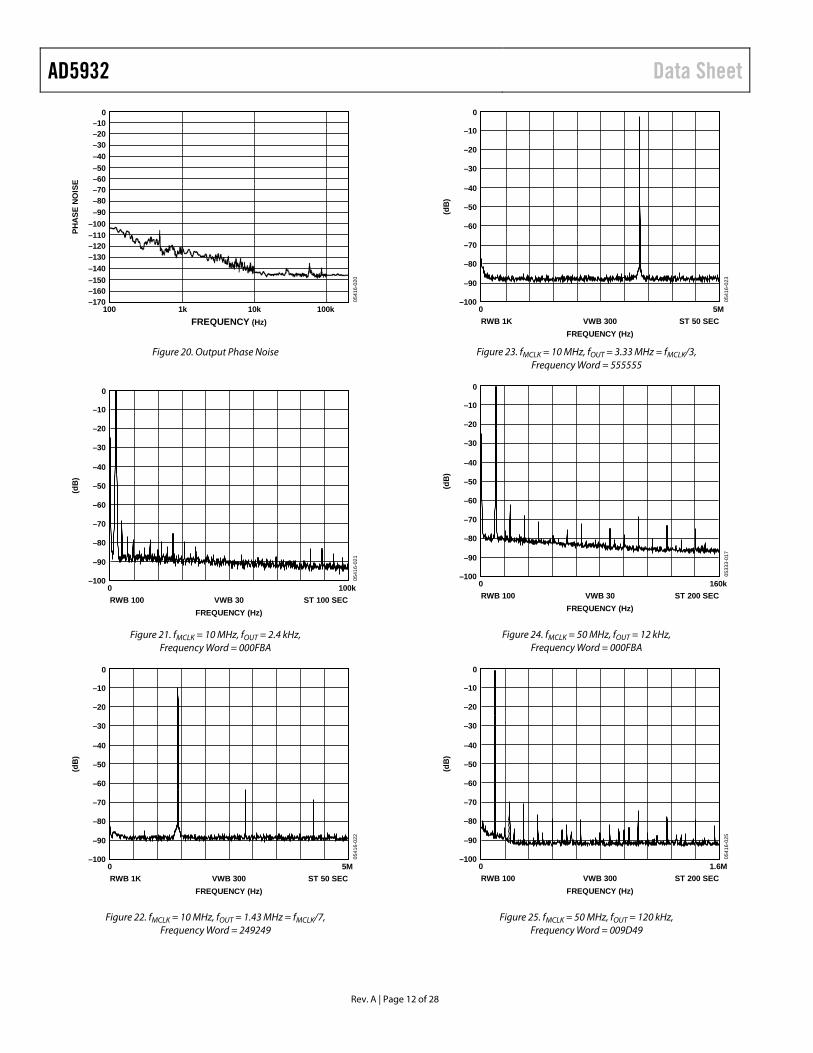
FREQUENCY (Hz)
0–10–20–30–40–50–60–70–80–90
–100–110–120–130–140–150–160–170
100k10k1k100
0541
6-02
0
PHA
SE N
OIS
E
Figure 20. Output Phase Noise
0
–10
–20
–30
–50
–60
–40
–70
–80
–90
–1000 100k
0541
6-02
1
(dB
)
VWB 30RWB 100 ST 100 SECFREQUENCY (Hz)
Figure 21. fMCLK = 10 MHz, fOUT = 2.4 kHz, Frequency Word = 000FBA
0
–10
–20
–30
–50
–60
–40
–70
–80
–90
–1000 5M
0541
6-02
2
(dB
)
VWB 300RWB 1K ST 50 SECFREQUENCY (Hz)
Figure 22. fMCLK = 10 MHz, fOUT = 1.43 MHz = fMCLK/7, Frequency Word = 249249
0
–10
–20
–30
–50
–60
–40
–70
–80
–90
–1000 5M
0541
6-02
3
(dB
)
VWB 300RWB 1K ST 50 SECFREQUENCY (Hz)
Figure 23. fMCLK = 10 MHz, fOUT = 3.33 MHz = fMCLK/3, Frequency Word = 555555
0
–10
–20
–30
–50
–60
–40
–70
–80
–90
–1000 160k
0533
3-01
7
(dB
)
VWB 30RWB 100 ST 200 SECFREQUENCY (Hz)
Figure 24. fMCLK = 50 MHz, fOUT = 12 kHz, Frequency Word = 000FBA
0
–10
–20
–30
–50
–60
–40
–70
–80
–90
–1000 1.6M
0541
6-02
5
(dB
)
VWB 300RWB 100 ST 200 SECFREQUENCY (Hz)
Figure 25. fMCLK = 50 MHz, fOUT = 120 kHz, Frequency Word = 009D49

Data Sheet AD5932
Rev. A | Page 13 of 28
0
–10
–20
–30
–50
–60
–40
–70
–80
–90
–1000 25M
0541
6-02
6
(dB
)
VWB 300RWB 1K ST 200 SECFREQUENCY (Hz)
Figure 26. fMCLK = 50 MHz, fOUT = 1.2 MHz, Frequency Word = 0624DD
0
–10
–20
–30
–50
–60
–40
–70
–80
–90
–1000 25M
0541
6-02
7
(dB
)
VWB 300RWB 1K ST 200 SECFREQUENCY (Hz)
Figure 27. fMCLK = 50 MHz, fOUT = 4.8 MHz, Frequency Word = 189374
0
–10
–20
–30
–50
–60
–40
–70
–80
–90
–1000 25M
0541
6-02
8
(dB
)
VWB 300RWB 1K ST 200 SECFREQUENCY (Hz)
Figure 28. fMCLK = 50 MHz, fOUT = 7.143 MHz = fMCLK/7, Frequency Word = 249249
0
–10
–20
–30
–50
–60
–40
–70
–80
–90
–1000 25M
0541
6-02
9
(dB
)
VWB 300RWB 1K ST 200 SECFREQUENCY (Hz)
Figure 29. fMCLK = 50 MHz, fOUT = 16.667 MHz = fMCLK/3, Frequency Word = 555555
AD5932 Data Sheet
Rev. A | Page 14 of 28
TERMINOLOGY Integral Nonlinearity (INL) Integral nonlinearity is the maximum deviation of any code from a straight line passing through the endpoints of the transfer function. The endpoints of the transfer function are zero scale and full scale. The error is expressed in LSBs.
Differential Nonlinearity (DNL) Differential nonlinearity is the difference between the measured and ideal 1 LSB change between two adjacent codes in the DAC. A specified differential nonlinearity of ±1 LSB maximum ensures monotonicity.
Spurious-Free Dynamic Range (SFDR) Along with the frequency of interest, harmonics of the fundamental frequency and images of these frequencies are present at the output of a DDS device. The SFDR refers to the largest spur or harmonic that is present in the band of interest. The wideband SFDR gives the magnitude of the largest harmonic or spur relative to the magnitude of the fundamental frequency in the 0 to Nyquist bandwidth. The narrow-band SFDR gives the attenuation of the largest spur or harmonic in a bandwidth of ±200 kHz about the fundamental frequency.
Total Harmonic Distortion (THD) Total harmonic distortion is the ratio of the rms sum of harmonics to the rms value of the fundamental. For the AD5932, THD is defined as:
1
65432
VVVVVV
THD22222
log20)dB(++++
=
where:
V1 is the rms amplitude of the fundamental. V2, V3, V4, V5, and V6 are the rms amplitudes of the second through the sixth harmonic.
Signal-to-Noise Ratio (SNR) The signal-to-noise ratio is the ratio of the rms value of the measured output signal to the rms sum of all other spectral components below the Nyquist frequency. The value for SNR is expressed in dB.
Clock Feedthrough There is feedthrough from the MCLK input to the analog output. Clock feedthrough refers to the magnitude of the MCLK signal relative to the fundamental frequency in the AD5932 output spectrum.
Data Sheet AD5932
Rev. A | Page 15 of 28
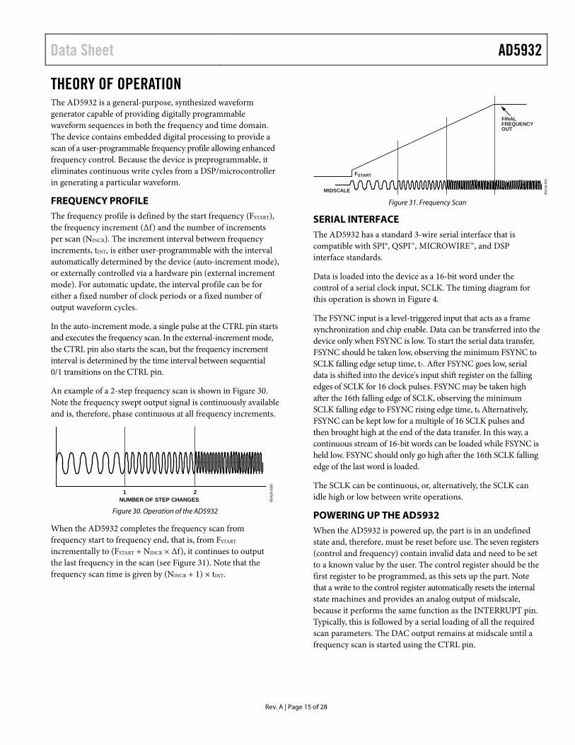
THEORY OF OPERATIONThe AD5932 is a general-purpose, synthesized waveform generator capable of providing digitally programmable waveform sequences in both the frequency and time domain. The device contains embedded digital processing to provide a scan of a user-programmable frequency profile allowing enhanced frequency control. Because the device is preprogrammable, it eliminates continuous write cycles from a DSP/microcontroller in generating a particular waveform.
FREQUENCY PROFILE The frequency profile is defined by the start frequency (FSTART), the frequency increment (Δf) and the number of increments per scan (NINCR). The increment interval between frequency increments, tINT, is either user-programmable with the interval automatically determined by the device (auto-increment mode), or externally controlled via a hardware pin (external increment mode). For automatic update, the interval profile can be for either a fixed number of clock periods or a fixed number of output waveform cycles.
In the auto-increment mode, a single pulse at the CTRL pin starts and executes the frequency scan. In the external-increment mode, the CTRL pin also starts the scan, but the frequency increment interval is determined by the time interval between sequential 0/1 transitions on the CTRL pin.
An example of a 2-step frequency scan is shown in Figure 30. Note the frequency swept output signal is continuously available and is, therefore, phase continuous at all frequency increments.
0541
6-03
0
21NUMBER OF STEP CHANGES
Figure 30. Operation of the AD5932
When the AD5932 completes the frequency scan from frequency start to frequency end, that is, from FSTART incrementally to (FSTART + NINCR × Δf), it continues to output the last frequency in the scan (see Figure 31). Note that the frequency scan time is given by (NINCR + 1) × tINT.
FSTART
MIDSCALE
FINALFREQUENCYOUT
0541
6-03
1
Figure 31. Frequency Scan
SERIAL INTERFACE The AD5932 has a standard 3-wire serial interface that is compatible with SPI®, QSPI™, MICROWIRE™, and DSP interface standards.
Data is loaded into the device as a 16-bit word under the control of a serial clock input, SCLK. The timing diagram for this operation is shown in Figure 4.
The FSYNC input is a level-triggered input that acts as a frame synchronization and chip enable. Data can be transferred into the device only when FSYNC is low. To start the serial data transfer, FSYNC should be taken low, observing the minimum FSYNC to SCLK falling edge setup time, t7. After FSYNC goes low, serial data is shifted into the device's input shift register on the falling edges of SCLK for 16 clock pulses. FSYNC may be taken high after the 16th falling edge of SCLK, observing the minimum SCLK falling edge to FSYNC rising edge time, t8. Alternatively, FSYNC can be kept low for a multiple of 16 SCLK pulses and then brought high at the end of the data transfer. In this way, a continuous stream of 16-bit words can be loaded while FSYNC is held low. FSYNC should only go high after the 16th SCLK falling edge of the last word is loaded.
The SCLK can be continuous, or, alternatively, the SCLK can idle high or low between write operations.
POWERING UP THE AD5932 When the AD5932 is powered up, the part is in an undefined state and, therefore, must be reset before use. The seven registers (control and frequency) contain invalid data and need to be set to a known value by the user. The control register should be the first register to be programmed, as this sets up the part. Note that a write to the control register automatically resets the internal state machines and provides an analog output of midscale, because it performs the same function as the INTERRUPT pin. Typically, this is followed by a serial loading of all the required scan parameters. The DAC output remains at midscale until a frequency scan is started using the CTRL pin.
AD5932 Data Sheet
Rev. A | Page 16 of 28
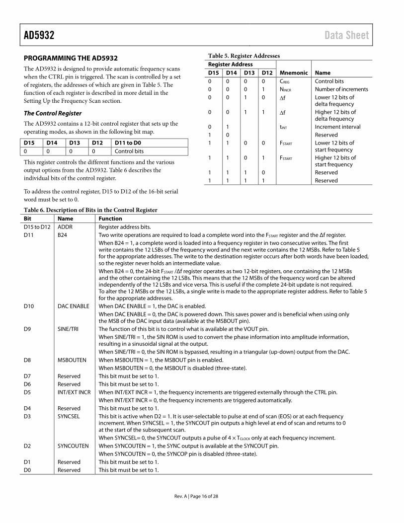
PROGRAMMING THE AD5932 The AD5932 is designed to provide automatic frequency scans when the CTRL pin is triggered. The scan is controlled by a set of registers, the addresses of which are given in Table 5. The function of each register is described in more detail in the Setting Up the Frequency Scan section.
The Control Register
The AD5932 contains a 12-bit control register that sets up the operating modes, as shown in the following bit map.
D15 D14 D13 D12 D11 to D0 0 0 0 0 Control bits
This register controls the different functions and the various output options from the AD5932. Table 6 describes the individual bits of the control register.
To address the control register, D15 to D12 of the 16-bit serial word must be set to 0.
Table 5. Register Addresses Register Address D15 D14 D13 D12 Mnemonic Name 0 0 0 0 CREG Control bits 0 0 0 1 NINCR Number of increments 0 0 1 0 ∆f Lower 12 bits of
delta frequency 0 0 1 1 ∆f Higher 12 bits of
delta frequency 0 1 tINT Increment interval 1 0 Reserved 1 1 0 0 FSTART Lower 12 bits of
start frequency 1 1 0 1 FSTART Higher 12 bits of
start frequency 1 1 1 0 Reserved 1 1 1 1 Reserved
Table 6. Description of Bits in the Control Register Bit Name Function D15 to D12 ADDR Register address bits. D11 B24 Two write operations are required to load a complete word into the FSTART register and the Δf register.
When B24 = 1, a complete word is loaded into a frequency register in two consecutive writes. The first write contains the 12 LSBs of the frequency word and the next write contains the 12 MSBs. Refer to Table 5 for the appropriate addresses. The write to the destination register occurs after both words have been loaded, so the register never holds an intermediate value. When B24 = 0, the 24-bit FSTART /Δf register operates as two 12-bit registers, one containing the 12 MSBs and the other containing the 12 LSBs. This means that the 12 MSBs of the frequency word can be altered independently of the 12 LSBs and vice versa. This is useful if the complete 24-bit update is not required. To alter the 12 MSBs or the 12 LSBs, a single write is made to the appropriate register address. Refer to Table 5 for the appropriate addresses.
D10 DAC ENABLE When DAC ENABLE = 1, the DAC is enabled. When DAC ENABLE = 0, the DAC is powered down. This saves power and is beneficial when using only the MSB of the DAC input data (available at the MSBOUT pin).
D9 SINE/TRI The function of this bit is to control what is available at the VOUT pin. When SINE/TRI = 1, the SIN ROM is used to convert the phase information into amplitude information, resulting in a sinusoidal signal at the output. When SINE/TRI = 0, the SIN ROM is bypassed, resulting in a triangular (up-down) output from the DAC.
D8 MSBOUTEN When MSBOUTEN = 1, the MSBOUT pin is enabled. When MSBOUTEN = 0, the MSBOUT is disabled (three-state).
D7 Reserved This bit must be set to 1. D6 Reserved This bit must be set to 1. D5 INT/EXT INCR When INT/EXT INCR = 1, the frequency increments are triggered externally through the CTRL pin.
When INT/EXT INCR = 0, the frequency increments are triggered automatically. D4 Reserved This bit must be set to 1. D3 SYNCSEL This bit is active when D2 = 1. It is user-selectable to pulse at end of scan (EOS) or at each frequency
increment. When SYNCSEL = 1, the SYNCOUT pin outputs a high level at end of scan and returns to 0 at the start of the subsequent scan. When SYNCSEL= 0, the SYNCOUT outputs a pulse of 4 × TCLOCK only at each frequency increment.
D2 SYNCOUTEN When SYNCOUTEN = 1, the SYNC output is available at the SYNCOUT pin. When SYNCOUTEN = 0, the SYNCOP pin is disabled (three-state).
D1 Reserved This bit must be set to 1. D0 Reserved This bit must be set to 1.
Data Sheet AD5932
Rev. A | Page 17 of 28
SETTING UP THE FREQUENCY SCAN As stated in the Frequency Profile section, the AD5932 requires certain registers to be programmed to enable a frequency scan. The Setting Up the Frequency Scan section discusses these registers in more detail.
Start Frequency (FSTART)
To start a frequency scan, the user needs to tell the AD5932 what frequency to start scanning from. This frequency is stored in a 24-bit register called FSTART. If the user wishes to alter the entire contents of the FSTART register, two consecutive writes must be performed: one to the LSBs and the other to the MSBs. Note that for an entire write to this register, Control Bit B24 (D11) should be set to 1, with the LSBs programmed first.
In some applications, the user does not need to alter all 24 bits of the FSTART register. By setting Control Bit B24 (D11) to 0, the 24-bit register operates as two 12-bit registers, one containing the 12 MSBs and the other containing the 12 LSBs. This means that the 12 MSBs of the FSTART word can be altered independently of the 12 LSBs and vice versa. The addresses of both the LSBs and the MSBs of this register are shown in the following bit map.
D15 D14 D13 D12 D11 to D0 1 1 0 0 12 LSBs of FSTART <11…0> 1 1 0 1 12 MSBs of FSTART <23…12>
Frequency Increments (Δf)
The value in the Δf register sets the increment frequency for the scan and is added incrementally to the current output frequency. Note that the increment frequency can be positive or negative, thereby giving an increasing or decreasing frequency scan.
At the start of a scan, the frequency contained in the FSTART register is output. Next, the frequency (FSTART + Δf ) is output. This is followed by (FSTART + Δf + Δf), and so on. Multiplying the Δf value by the number of increments (NINCR) and adding it to the start frequency (FSTART) give the final frequency in the scan. Mathematically, this final frequency/stop frequency is represented by
FSTART + (NINCR × Δf)
The Δf register is a 23-bit register that requires two 16-bit writes to be programmed. Table 7 gives the addresses associated with both the MSB and LSB registers of the Δf word.
Table 7. Δf Register Bits
D15 D14 D13 D12 D11 D10 to D0 Scan Direction
0 0 1 0 12 LSBs of Δf <11…0>
N/A
0 0 1 1 0 11 MSBs of Δf <22…12>
Positive Δf (FSTART + Δf )
0 0 1 1 1 11 MSBs of Δf <22…12>
Negative f (FSTART − Δf )
Number of Increments (NINCR)
An end frequency is not required on the AD5932. Instead, this end frequency is calculated by multiplying the frequency increment value (Δf) by the number of frequency steps (NINCR) and adding it to/subtracting it from the start frequency (FSTART); that is, FSTART + NINCR × Δ f. The NINCR register is a 12-bit register, with the address shown in the following bit map.
D15 D14 D13 D12 D11 D0 0 0 0 1 12 bits of NINCR <11…0>
The number of increments is programmed in binary fashion, with 000000000010 representing the minimum number of frequency increments (two increments) and 111111111111 representing the maximum number of increments (4095).
Table 8. NINCR Data Bits D11 … D0 Number of Increments 0000 0000 0010 Two frequency increments. This is the
minimum number of frequency increments.
0000 0000 0011 Three frequency increments. 0000 0000 0100 Four frequency increments. … … … … 1111 1111 1110 4094 frequency increments. 1111 1111 1111 4095 frequency increments.
Increment Interval (tINT)
The increment interval dictates the duration of the DAC output signal for each individual frequency of the frequency scan. The AD5932 offers the user two choices:
The duration is a multiple of cycles of the output frequency.
The duration is a multiple of MCLK periods.
The desired choice is selected by Bit D13 in the tINT register as shown in the following bit map.
D15 D14 D13 D12 D11 D10 to D0 0 1 0 x x 11 bits <10…0>
Fixed number of output waveform cycles.
0 1 1 x x 11 bits <10…0> Fixed number of clock periods.
Programming of this register is in binary form, with the minimum number being decimal 2. Note that 11 bits, D10 to D0, of the register are available to program the time interval. As an example, if MCLK = 50 MHz, then each clock period/base interval is (1/50 MHz) = 20 ns. If each frequency must be output for 100 ns, then <00000000101> or decimal 5 must be pro-grammed to this register. Note that the AD5930 can output each frequency for a maximum duration of 211 − 1 (or 2047) times the increment interval.
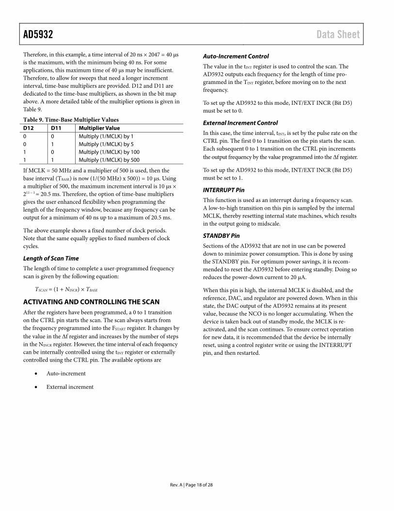
AD5932 Data Sheet
Rev. A | Page 18 of 28
Therefore, in this example, a time interval of 20 ns × 2047 = 40 µs is the maximum, with the minimum being 40 ns. For some applications, this maximum time of 40 µs may be insufficient. Therefore, to allow for sweeps that need a longer increment interval, time-base multipliers are provided. D12 and D11 are dedicated to the time-base multipliers, as shown in the bit map above. A more detailed table of the multiplier options is given in Table 9.
Table 9. Time-Base Multiplier Values D12 D11 Multiplier Value 0 0 Multiply (1/MCLK) by 1 0 1 Multiply (1/MCLK) by 5 1 0 Multiply (1/MCLK) by 100 1 1 Multiply (1/MCLK) by 500
If MCLK = 50 MHz and a multiplier of 500 is used, then the base interval (TBASE) is now (1/(50 MHz) x 500)) = 10 µs. Using a multiplier of 500, the maximum increment interval is 10 µs × 211 − 1 = 20.5 ms. Therefore, the option of time-base multipliers gives the user enhanced flexibility when programming the length of the frequency window, because any frequency can be output for a minimum of 40 ns up to a maximum of 20.5 ms.
The above example shows a fixed number of clock periods. Note that the same equally applies to fixed numbers of clock cycles.
Length of Scan Time
The length of time to complete a user-programmed frequency scan is given by the following equation:
TSCAN = (1 + NINCR) × TBASE
ACTIVATING AND CONTROLLING THE SCAN After the registers have been programmed, a 0 to 1 transition on the CTRL pin starts the scan. The scan always starts from the frequency programmed into the FSTART register. It changes by the value in the ∆f register and increases by the number of steps in the NINCR register. However, the time interval of each frequency can be internally controlled using the tINT register or externally controlled using the CTRL pin. The available options are
• Auto-increment
• External increment
Auto-Increment Control
The value in the tINT register is used to control the scan. The AD5932 outputs each frequency for the length of time pro-grammed in the TINT register, before moving on to the next frequency.
To set up the AD5932 to this mode, INT/EXT INCR (Bit D5) must be set to 0.
External Increment Control
In this case, the time interval, tINT, is set by the pulse rate on the CTRL pin. The first 0 to 1 transition on the pin starts the scan. Each subsequent 0 to 1 transition on the CTRL pin increments the output frequency by the value programmed into the ∆f register.
To set up the AD5932 to this mode, INT/EXT INCR (Bit D5) must be set to 1.
INTERRUPT Pin
This function is used as an interrupt during a frequency scan. A low-to-high transition on this pin is sampled by the internal MCLK, thereby resetting internal state machines, which results in the output going to midscale.
STANDBY Pin
Sections of the AD5932 that are not in use can be powered down to minimize power consumption. This is done by using the STANDBY pin. For optimum power savings, it is recom-mended to reset the AD5932 before entering standby. Doing so reduces the power-down current to 20 μA.
When this pin is high, the internal MCLK is disabled, and the reference, DAC, and regulator are powered down. When in this state, the DAC output of the AD5932 remains at its present value, because the NCO is no longer accumulating. When the device is taken back out of standby mode, the MCLK is re-activated, and the scan continues. To ensure correct operation for new data, it is recommended that the device be internally reset, using a control register write or using the INTERRUPT pin, and then restarted.

Data Sheet AD5932
Rev. A | Page 19 of 28
OUTPUTS FROM THE AD5932 The AD5932 offers a variety of outputs from the chip. The analog outputs are available from the VOUT pin and include a sine wave and a triangle output. The digital outputs are available from the MSBOUT pin and the SYNCOUT pin.
Analog Outputs Sinusoidal Output
The SIN ROM is used to convert the phase information from the frequency register into amplitude information, resulting in a sinusoidal signal at the output.
The AD5932 includes a 10-bit, high impedance, current source DAC that is configured for single-ended operation. An external load resistor is not required because the device has a 200 Ω resistor on board. To have a sinusoidal output from the VOUT pin, set SINE/TRI (Bit D9) in the control register to 1.
Triangle Output
The SIN ROM can be bypassed so that the truncated digital output from the NCO is sent to the DAC. In this case, the output is no longer sinusoidal. The DAC produces a 10-bit linear triangular function. To have a triangle output from the VOUT pin, set SINE/TRI (Bit D9) to 0. Note that DAC ENABLE (Bit D10) must be set to 1 (that is, the DAC is enabled) when using this pin.
VOUT MAX
3p/2 7p/2
p/2 5p/2 9p/2
11p/2VOUT MIN
0541
6-03
2
Figure 32. Triangle Output
Digital Outputs
Square-Wave Output from MSBOUT
The inverse of the MSB from the NCO can be output from the AD5932. By setting MSBOUTEN (Bit D8) to 1, the inverted MSB of the DAC data is available at the MSBOUT pin. This is useful as a digital clock source.
DVDD
DGND 0541
6-04
0
Figure 33. MSB Output
SYNCOUT Pin
The SYNCOUT pin can be used to give the status of the scan. It is user-selectable for the end of scan or to output a 4 × TCLOCK pulse at frequency increments. The timing information for both of these modes is shown in Figure 6.
The SYNCOUT pin must be enabled before use. This is done using Bit D2 in the control register. The output available from this pin is then controlled by Bit D3 in the control register. See Table 6 for more information.
AD5932 Data Sheet
Rev. A | Page 20 of 28
APPLICATIONSGROUNDING AND LAYOUT The printed circuit board that houses the AD5932 should be designed so that the analog and digital sections are separated and confined to certain areas of the board. This facilitates the use of ground planes that can be easily separated. A minimum etch technique is generally best for ground planes because it gives the best shielding. Digital and analog ground planes should be joined in only one place. If the AD5932 is the only device requiring an AGND-to-DGND connection, then the ground planes should be connected at the AGND and DGND pins of the AD5932. If the AD5932 is in a system where multiple devices require AGND-to-DGND connections, the connection should be made at one point only, a star ground point that should be established as close as possible to the AD5932.
Avoid running digital lines under the device because these couple noise onto the die. The analog ground plane should run under the AD5932 to avoid noise coupling. The power supply lines to the AD5932 should use as large a track as possible to provide low impedance paths and reduce the effects of glitches on the power supply line. Fast switching signals, such as clocks, should be shielded with digital ground to avoid radiating noise to other sections of the board. Avoid crossover of digital and analog signals. Traces on opposite sides of the board should run at right angles to each other, reducing the effects of feedthrough. A microstrip technique is by far the best but is not always possible with a double-sided board. In this technique, the component side of the board is dedicated to ground planes, while signals are placed on the other side.
Good decoupling is important. The analog and digital supplies to the AD5932 are independent and separately pinned out to minimize coupling between analog and digital sections of the device. All analog and digital supplies should be decoupled to AGND and DGND, respectively, with 0.1 µF ceramic capacitors in parallel with 10 µF tantalum capacitors. To achieve the best from the decoupling capacitors, they should be placed as close as possible to the device, ideally right up against the device. In systems where a common supply is used to drive both the AVDD and DVDD of the AD5932, it is recommended that the system’s AVDD supply be used. This supply should have the recom-mended analog supply decoupling between the AVDD pin of the AD5932 and AGND and the recommended digital supply decoupling capacitors between the DVDD pin and DGND.
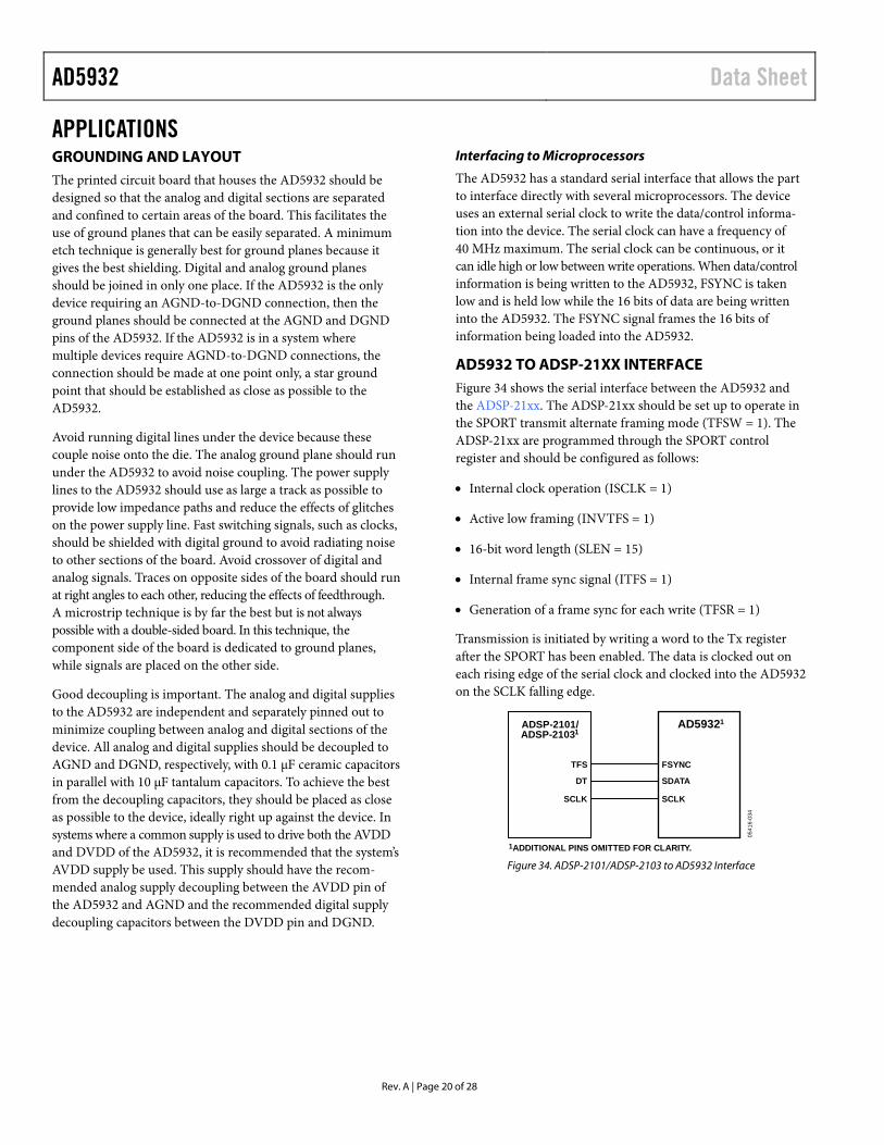
Interfacing to Microprocessors
The AD5932 has a standard serial interface that allows the part to interface directly with several microprocessors. The device uses an external serial clock to write the data/control informa-tion into the device. The serial clock can have a frequency of 40 MHz maximum. The serial clock can be continuous, or it can idle high or low between write operations. When data/control information is being written to the AD5932, FSYNC is taken low and is held low while the 16 bits of data are being written into the AD5932. The FSYNC signal frames the 16 bits of information being loaded into the AD5932.
AD5932 TO ADSP-21XX INTERFACE Figure 34 shows the serial interface between the AD5932 and the ADSP-21xx. The ADSP-21xx should be set up to operate in the SPORT transmit alternate framing mode (TFSW = 1). The ADSP-21xx are programmed through the SPORT control register and should be configured as follows:
• Internal clock operation (ISCLK = 1)
• Active low framing (INVTFS = 1)
• 16-bit word length (SLEN = 15)
• Internal frame sync signal (ITFS = 1)
• Generation of a frame sync for each write (TFSR = 1)
Transmission is initiated by writing a word to the Tx register after the SPORT has been enabled. The data is clocked out on each rising edge of the serial clock and clocked into the AD5932 on the SCLK falling edge.
AD59321ADSP-2101/ADSP-21031
1ADDITIONAL PINS OMITTED FOR CLARITY.
TFS
DT
SCLK
FSYNC
0541
6-03
4
SDATA
SCLK
Figure 34. ADSP-2101/ADSP-2103 to AD5932 Interface
Data Sheet AD5932
Rev. A | Page 21 of 28
AD5932 TO 68HC11/68L11 INTERFACE Figure 35 shows the serial interface between the AD5932 and the 68HC11/68L11 microcontroller. The microcontroller is configured as the master by setting Bit MSTR in the SPCR to 1, which provides a serial clock on SCK while the MOSI output drives the serial data line, SDATA. Because the microcontroller does not have a dedicated frame sync pin, the FSYNC signal is derived from a port line (PC7). The set-up conditions for correct operation of the interface are as follows:
• SCK idles high between write operations (CPOL = 0).
• Data is valid on the SCK falling edge (CPHA = 1).
When data is being transmitted to the AD5932, the FSYNC line is taken low (PC7). Serial data from the 68HC11/68L11 is transmitted in 8-bit bytes with only eight falling clock edges occurring in the transmit cycle. Data is transmitted MSB first. In order to load data into the AD5932, PC7 is held low after the first eight bits are transferred and a second serial write operation is performed to the AD5932. Only after the second eight bits have been transferred should FSYNC be taken high again.
AD5932168HC11/68L111
1ADDITIONAL PINS OMITTED FOR CLARITY.
PC7
MOSI
SCK
FSYNC
0541
6-03
5
SDATA
SCLK
Figure 35. 68HC11/68L11 to AD5932 Interface
AD5932 TO 80C51/80L51 INTERFACE Figure 36 shows the serial interface between the AD5932 and the 80C51/80L51 microcontroller. The microcontroller is operated in Mode 0 so that TxD of the 80C51/80L51 drives SCLK of the AD5932, while RxD drives the serial data line SDATA. The FSYNC signal is again derived from a bit program-mable pin on the port (P3.3 being used in the diagram). When data is to be transmitted to the AD5932, P3.3 is taken low. The 80C51/80L51 transmits data in 8-bit bytes; thus, only eight falling SCLK edges occur in each cycle.
To load the remaining eight bits to the AD5932, P3.3 is held low after the first eight bits have been transmitted, and a second write operation is initiated to transmit the second byte of data. P3.3 is taken high following completion of the second write operation. SCLK should idle high between the two write operations. The 80C51/80L51 outputs the serial data in an LSB-first format. The AD5932 accepts the MSB first (the four MSBs being the control information, the next four bits being the address, while the eight LSBs contain the data when writing to a destination register). Therefore, the transmit routine of the 80C51/80L51 must consider this and rearrange the bits so that the MSB is output first.
AD5932180C51/80L511
1ADDITIONAL PINS OMITTED FOR CLARITY.
P3.3
RxD
TxD
FSYNC
0541
6-03
6
SDATA
SCLK
Figure 36. 80C51/80L51 to AD5932 Interface
AD5932 TO DSP56002 INTERFACE Figure 37 shows the interface between the AD5932 and the DSP56002. The DSP56002 is configured for normal mode, asynchronous operation with a gated internal clock (SYN = 0, GCK = 1, SCKD = 1). The frame sync pin is generated internally (SC2 = 1), the transfers are 16 bits wide (WL1 = 1, WL0 = 0), and the frame sync signal frames the 16 bits (FSL = 0). The frame sync signal is available on Pin SC2, but it must be inverted before being applied to the AD5932. The interface to the DSP56000/DSP56001 is similar to that of the DSP56002.
AD59321DSP560021
1ADDITIONAL PINS OMITTED FOR CLARITY.
SC2
STD
SCK
FSYNC05
416-
032
SDATA
SCLK
Figure 37. DSP56002 to AD5932 Interface

AD5932 Data Sheet
Rev. A | Page 22 of 28
EVALUATION BOARDThe AD5932 evaluation board allows designers to evaluate the high performance AD5932 DDS modulator with minimum effort.
The evaluation board interfaces to the USB port of a PC. It is possible to power the entire board from the USB port. All that is needed to complete the evaluation of the chip is either a spectrum analyzer or a scope.
The DDS evaluation kit includes a populated and tested AD5932 printed circuit board. The EVAL-AD5932EB kit is shipped with a CD-ROM that includes self-installing software. The PC is connected to the evaluation board using the supplied cable. The software is compatible with Microsoft® Windows® 2000 and Windows XP.
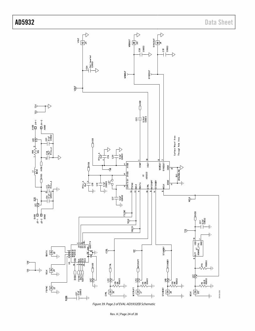
A schematic of the evaluation board is shown in Figure 38 and Figure 39.
Using the AD5932 Evaluation Board
The AD5932 evaluation kit is a test system designed to simplify the evaluation of the AD5932. An application note is also available with the evaluation board that gives full information on operating the evaluation board.
Prototyping Area
An area is available on the evaluation board for the user to add additional circuits to the evaluation test set. Users may want to build custom analog filters for the output or add buffers and operational amplifiers to be used in the final application.
XO vs. External Clock
The AD5932 can operate with master clocks up to 50 MHz. A 50 MHz oscillator is included on the evaluation board. However, this oscillator can be removed and, if required, an external CMOS clock can be connected to the part.

Data Sheet AD5932
Rev. A | Page 23 of 28
SCHEMATICS
0541
6-03
8
Figure 38. Page 1 of EVAL-AD5932EB Schematic
AD5932 Data Sheet
Rev. A | Page 24 of 28
0541
6-03
9
Figure 39. Page 2 of EVAL-AD5932EB Schematic
Data Sheet AD5932
Rev. A | Page 25 of 28
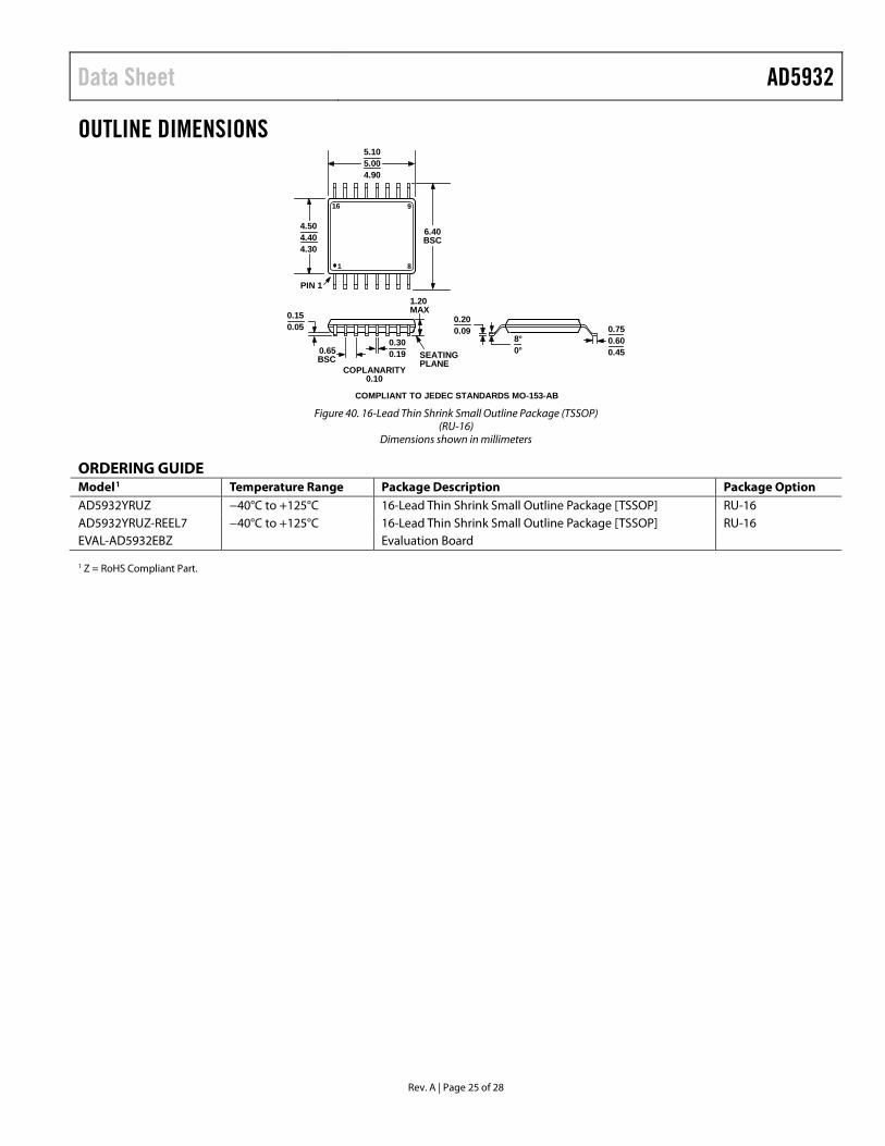
OUTLINE DIMENSIONS
16 9
81
PIN 1
SEATINGPLANE
8°0°
4.504.404.30
6.40BSC
5.105.004.90
0.65BSC
0.150.05
1.20MAX
0.200.09 0.75
0.600.45
0.300.19
COPLANARITY0.10
COMPLIANT TO JEDEC STANDARDS MO-153-AB Figure 40. 16-Lead Thin Shrink Small Outline Package (TSSOP)
(RU-16) Dimensions shown in millimeters
ORDERING GUIDE Model1 Temperature Range Package Description Package Option AD5932YRUZ −40°C to +125°C 16-Lead Thin Shrink Small Outline Package [TSSOP] RU-16 AD5932YRUZ-REEL7 −40°C to +125°C 16-Lead Thin Shrink Small Outline Package [TSSOP] RU-16 EVAL-AD5932EBZ Evaluation Board 1 Z = RoHS Compliant Part.

AD5932 Data Sheet
Rev. A | Page 26 of 28
NOTES

Data Sheet AD5932
Rev. A | Page 27 of 28
NOTES

AD5932 Data Sheet
Rev. A | Page 28 of 28
NOTES
©2006–2012 Analog Devices, Inc. All rights reserved. Trademarks and registered trademarks are the property of their respective owners. D05416-0-2/12(A)