Embed Size (px)
Citation preview
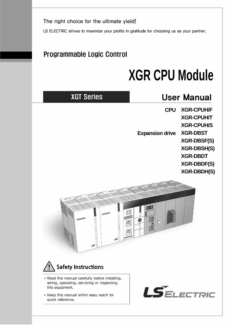
Programmable Logic Control
XGR CPU Module
XGT Series
CPU
Expansion drive
XGR-CPUH/F XGR-CPUH/T XGR-CPUH/S XGR-DBST XGR-DBSF(S) XGR-DBSH(S) XGR-DBDT XGR-DBDF(S) XGR-DBDH(S)
Safety Instruction
1
Before using the product … For your safety and effective operation, please read the safety instructions thoroughly before using the product. Safety Instructions should always be observed in order to prevent accident
or risk with the safe and proper use the product. Instructions are separated into “Warning” and “Caution”, and the meaning of
the terms is as follows;
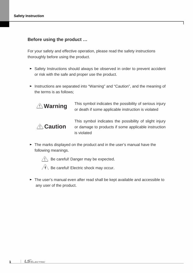
This symbol indicates the possibility of serious injury or death if some applicable instruction is violated
This symbol indicates the possibility of slight injury or damage to products if some applicable instruction is violated
The marks displayed on the product and in the user’s manual have the
following meanings.
Be careful! Danger may be expected.
Be careful! Electric shock may occur. The user’s manual even after read shall be kept available and accessible to
any user of the product.
Warning
Caution
Safety Instruction
2
Safety Instructions when designing
Please, install protection circuit on the exterior of PLC to protect the whole control system from any error in external power or PLC
module. Any abnormal output or operation may cause serious problem in safety of the whole system.
- Install applicable protection unit on the exterior of PLC to protect the system from physical damage such as emergent stop switch, protection circuit, the upper/lowest limit switch, forward/reverse operation interlock circuit, etc.
- If any system error (watch-dog timer error, module installation error, etc.) is detected during CPU operation in PLC, the whole output is designed to be turned off and stopped for system safety. However, in case CPU error if caused on output device itself such as relay or TR can not be detected, the output may be kept on, which may cause serious problems. Thus, you are recommended to install an addition circuit to monitor the output status.
Never connect the overload than rated to the output module nor allow the output circuit to have a short circuit, which may cause a fire.
Never let the external power of the output circuit be designed to be On earlier than PLC power, which may cause abnormal output or
operation.
In case of data exchange between computer or other external equipment and PLC through communication or any operation of PLC (e.g. operation mode change), please install interlock in the sequence program to protect the system from any error. If not, it may cause abnormal output or operation.
Warning
Safety Instruction
3
Safety Instructions when designing
Safety Instructions when designing
I/O signal or communication line shall be wired at least 100mm away from a high-voltage cable or power line. If not, it may cause abnormal output or operation.
Caution
Use PLC only in the environment specified in PLC manual or general standard of data sheet. If not, electric shock, fire, abnormal operation of the product or flames may be caused.
Before installing the module, be sure PLC power is off. If not, electric shock or damage on the product may be caused.
Be sure that each module of PLC is correctly secured. If the product is installed loosely or incorrectly, abnormal operation, error or dropping may be caused.
Be sure that I/O or extension connecter is correctly secured. If not, electric shock, fire or abnormal operation may be caused.
If lots of vibration is expected in the installation environment, don’t let PLC directly vibrated. Electric shock, fire or abnormal operation may be caused.
Don’t let any metallic foreign materials inside the product, which may cause electric shock, fire or abnormal operation.
Caution
Safety Instruction
4
Safety Instructions when wiring
Prior to wiring, be sure that power of PLC and external power is turned off. If not, electric shock or damage on the product may be caused.
Before PLC system is powered on, be sure that all the covers of
the terminal are securely closed. If not, electric shock may be caused
Warning
Let the wiring installed correctly after checking the voltage rated of each product and the arrangement of terminals. If not, fire, electric shock or abnormal operation may be caused.
Secure the screws of terminals tightly with specified torque when wiring. If the screws of terminals get loose, short circuit, fire or abnormal operation may be caused.
Surely use the ground wire of Class 3 for FG terminals, which is
exclusively used for PLC. If the terminals not grounded correctly, abnormal operation may be caused.
Don’t let any foreign materials such as wiring waste inside the module while wiring, which may cause fire, damage on the product or abnormal operation.
Caution
Safety Instruction
5
Safety Instructions for test-operation or repair
Safety Instructions for waste disposal
Don’t touch the terminal when powered. Electric shock or abnormal operation may occur.
Prior to cleaning or tightening the terminal screws, let all the external power off including PLC power. If not, electric shock or abnormal operation may occur.
Don’t let the battery recharged, disassembled, heated, short or soldered. Heat, explosion or ignition may cause injuries or fire.
Warning
Don’t remove PCB from the module case nor remodel the module. Fire, electric shock or abnormal operation may occur.
Prior to installing or disassembling the module, let all the
external power off including PLC power. If not, electric shock or abnormal operation may occur.
Keep any wireless installations or cell phone at least 30cm away from PLC. If not, abnormal operation may be caused.
Caution
Product or battery waste shall be processed as industrial waste. The waste may discharge toxic materials or explode itself.
Caution

Safety Instruction
6
Revision History
1
Revision History
Version Data Main contents Revised location
V 1.0 ’08. 6 First Edition -
V 1.1 ’08.7 1. Modifying contents
(2) How to configure redundancy system
(3) Performance specification
(4) Scan Time
(5) Program memory
(6) I/O module skip function
(7) Module changing wizard during RUN
(8) Performance specification
(9) Example of calculating consumption current/power
(10) Caution in handling
(11) Grounding
2. Adding contents
(1) XGR redundancy system configuration
(2) Remote I/O system
(3) Scan Time
(4) I/O module skip
3. Deleting contents
(1) Max install-able module number in specification
-
2-5
4-1,4-2
5-6,5-8
5-28
6-19,6-20
6-21
7-1,7-3
8-5
11-5
11-13
-
1-3
2-13
5-8
6-20
-
7-1
V 1.2 ’09.9 1. Modifying contents
(1) Performance specification
(2) redundancy parameter setting window
(3) Flag
-
4-2
5-2, CH6
A-6, A-11
V 1.3 ’09.9 1. Adding contents
(1) Contents on redundancy system communication operation setting (ONE IP Solution)
2. modifying contents
(1) Product list (add new products)
- XGR-DC32, XGR-DMMA
- XGF-SOEA
- XGL-EIPT
6-18~20
2-1
2-3
2-4
Revision History
2
Version Data Main contents Revised location
V 1.4 ’09.12 1. Adding contents
(1) adding contents related to DC power
Ch8.1, Ch8.2, Ch8.3
V 1.5 ’10.03 1. Adding contents
(1) Contents on reset/D.Clear
(2) Contents on Cnet/FEnet module equipment
(3) Contents on redundancy parameter
(4) Warning flag
(5) Smart Link wiring diagram and Event input module specifications
2. Modifying contents
(1) Contents on parameter setting window
(2) Contents on Fault mask setting
(3) Module replacement
4-6
2-7
5-8~9
App-8
9-24~25
5-4, 6-1, 6-14~15
6-20
6-23~24
V 1.6 ’10.10 1. Modifying contents
(1) Modifying contents
(2) Adding contents
(3) Adding modules
(4) Modifying contents on redundancy parameter
(5) Modifying contents on basic parameter
Ch3.1
Ch5.1.2
Ch5.1.4
Ch5.1.4
Ch6.7.1
V 1.7 ’10.10 1. Modifying contents
(1) Overview
(2) System configuration
(3) Power module
(4) Base and expansion cable
Ch1.1
Ch2.1
Ch8.4.1
Ch101.1
V 1.8 ’10.10 1. Adding contents
(1) Adding contents on redundancy parameter
(2) Adding contents on redundancy parameter
(3) Adding contents on redundancy parameter
Ch5.1.4
Ch6.8.1
Ch6.9
Revision History
3
Version Data Main contents Revised location
V 1.9 ’11.06 1. Adding contents
(1) Adding module on Extension redundancy
(2) Adding contents on Extension redundancy
(3) Adding contents on Flag
(4) Adding optical single module
1-1, 2-1, 7-2
1-3, 1-4, 2-8, 6-25,
8-3, 10-2, 14-28
App-3/7/11/13
1-1, 2-1, 2-6, 4-1, 4-2, 7-1
V 2.0 ’13.01 1. Adding contents
(1) Adding Redundancy Expansion Base
(2) Built-in PID Function
2.Modifying contents
(1) Modifying EtherNet/IP
(2) Modifying U, K Device memory
3. Removing contents
(1) Removing Appendix 1.11
2-1, 10-1
Ch 14
1-6, 2-7, 2-13
4-1, 5-32
App-21
V 2.1 ’14.06 1. Adding contents
(1) Adding _REFRESH_NG_BASE
App-13
V 2.2 ’15.07 1.Modifying contents
(1) Vibration resistance Specifications
3-1
V 2.3 ‘15.09
1.Modifying contents (1) Rated input voltage modified (2) Circuit configuration modified (3) Smart Link Model name modified (4) Terminology modified (FG PE) (5) CPU Processing Speed Unit changed (us ns) (6) List of Configuration Products updated
8-1
9-2, 9-3, 9-4, 9-5 9-6
8-2, 10-1, 10-2, 11-2, 13-1 4.1 2.1
V 2.4 ‘16.03 1.Modifying contents (1) Smart Link manual supplemented
9-6
V2.5 ’16.09 1. Adding contents
(1) Redundancy expansion driver(single mode) updated
1-1, 2-1, 7-7

Revision History
4
Version Data Main contents Revised location
V 2.6 ’20.05 LSIS to change its corporate name to LS ELECTRIC Entire
About User's Manual
1
Thank you for purchasing PLC of LS ELECTRIC Co., Ltd. Before use, make sure to carefully read and understand the User’s Manual about the functions, performances, installation and programming of the product you purchased in order for correct use and importantly, let the end user and maintenance administrator to be provided with the User’s Manual. The User’s Manual describes the product. If necessary, you may refer to the following description and order accordingly. In addition, you may connect our website (http://www.lselectric.co.kr/) and download the information as a PDF file.
Relevant User’s Manuals Title Description
XG5000 User’s Manual (for XGK, XGB)
XG5000 software user manual describing online function such as programming, print, monitoring, debugging by using XGK, XGB CPU
XG5000 User’s Manual (for XGI, XGR)
XG5000 software user manual describing online function such as programming, print, monitoring, debugging by using XGI, XGR CPU
XGK/XGB Instructions & Programming User’s Manual
User’s manual for programming to explain how to use instructions that are used PLC system with XGK, XGB CPU.
XGI/XGR/XEC Instructions & Programming User’s Manual
User’s manual for programming to explain how to use instructions that are used PLC system with XGI, XGR CPU.
XGK CPU User’s Manual (XGK-CPUA/CPUE/CPUH/CPUS/CPUU /CPUUN/CPUHN/CPUSN)
User manual describing about XGK CPU module, power module, base, IO module, specification of extension cable and system configuration, EMC standard
XGI CPU User’s Manual (XGI-CPUU/CPUH/CPUS/CPUE/CPUU/D CPUUN)
User manual describing about XGI CPU module, power module, base, IO module, specification of extension cable and system configuration, EMC standard
XGR redundant series User’s Manual
User manual describing about XGR CPU module, power module, extension drive, base, IO module, specification of extension cable and system configuration, EMC standard

About User's Manual
2
Table of Contents
1
TABLE OF CONTENTS
Chapter 1 Overview ............................................................................................................................... 1-1~1-8
1.1 About this User Manual ......................................................................................................................... 1-1 1.2 Configuration of the XGR Redundant System ...................................................................................... 1-3 1.3 Features of the XGR Redundancy system ............................................................................................ 1-4 1.4 Glossary ................................................................................................................................................. 1-6
Chapter 2 System Configuration ........................................................................................................ 2-1~2-17
2.1 Product List .............................................................................................................................................. 2-1 2.2 Redundancy System ............................................................................................................................. 2-7 2.2.1 Redundant System Configuration ................................................................................................. 2-7 2.2.2 Redundancy of CPU system ....................................................................................................... 2-9 2.2.3 Power Module Redundancy ...................................................................................................... 2-11 2.2.4 Extension Drive Redundancy .................................................................................................... 2-12 2.2.5 Extension Base Communication Path Redundancy ................................................................ 2-12 2.2.6 Example of Redundant System Configuration ........................................................................ 2-12 2.3 Network System .................................................................................................................................... 2-17 2.3.1 Networking among Systems ...................................................................................................... 2-17 2.3.2 Remote I/O System ...................................................................................................................... 2-17
Chapter 3 General Specifications ................................................................................................................. 3-1
3.1 General Specifications ............................................................................................................................. 3-1
Chapter 4 CPU Module ......................................................................................................................... 4-1~4-8
4.1 Performance Specifications .................................................................................................................... 4-1 4.2 Names and Functions of Parts ............................................................................................................... 4-3 4.3 Battery ...................................................................................................................................................... 4-7 4.3.1 Battery specifications ...................................................................................................................... 4-7 4.3.2 Cautions for usage .......................................................................................................................... 4-7 4.3.3 Battery life ........................................................................................................................................ 4-7 4.3.4 Replacement ................................................................................................................................... 4-8
Chapter 5 Program Constitution and Operation Method .................................................................. 5-1~5-33
5.1 Program Basics ...................................................................................................................................... 5-1 5.1.1 Program Structure and Execution ................................................................................................ 5-1 5.1.2 Software Program Execution Methodology ................................................................................ 5-2 5.1.3 Operation of instantaneous interrupt ............................................................................................. 5-5
Table of Contents
2
5.1.4 Scan Time ....................................................................................................................................... 5-6 5.2 Program Execution .............................................................................................................................. 5-11 5.2.1 Program Type ................................................................................................................................ 5-11 5.2.2 Program Execution ....................................................................................................................... 5-11 5.2.3 Restart Mode ............................................................................................................................... 5-12 5.2.4 Task Program .............................................................................................................................. 5-14 5.3 Operation Mode ..................................................................................................................................... 5-23 5.3.1 Operation Mode .......................................................................................................................... 5-23 5.3.2 RUN mode .................................................................................................................................... 5-23 5.3.3 Stop Mode ..................................................................................................................................... 5-24 5.3.4 Debug Mode ................................................................................................................................. 5-25 5.3.5 Switching Operation Mode ......................................................................................................... 5-25 5.4 Redundancy System Operation ......................................................................................................... 5-27 5.4.1 Redundancy System Operation .................................................................................................. 5-27 5.4.2 Start-up of Redundant System ..................................................................................................... 5-29 5.5 Memory .................................................................................................................................................. 5-31 5.5.1 Program memory .......................................................................................................................... 5-31 5.5.2 Data memory ................................................................................................................................ 5-32 5.5.3 Data retain area setting ................................................................................................................. 5-32
Chapter 6 CPU Module Functions ..................................................................................................... 6-1~6-24
6.1 Self-diagnosis Function ........................................................................................................................... 6-1 6.1.1 Scan watchdog timer ...................................................................................................................... 6-1 6.1.2 I/O Module Check Function ........................................................................................................... 6-3 6.1.3 Battery level check .......................................................................................................................... 6-3 6.1.4 Saving error log ............................................................................................................................... 6-3 6.1.5 Troubleshooting .............................................................................................................................. 6-3 6.2 Clock Function ......................................................................................................................................... 6-4 6.3 Remote Functions ................................................................................................................................... 6-7 6.4 Forced On/Off Function of I/O ............................................................................................................... 6-10 6.4.1 Force I/O Setting ........................................................................................................................... 6-10 6.4.2 The point of time of method of forced On/Off process................................................................ 6-11 6.5 Operation history saving function ......................................................................................................... 6-12 6.5.1 Error history ................................................................................................................................... 6-12 6.5.2 Mode change history .................................................................................................................... 6-12 6.5.3 Shut down history ......................................................................................................................... 6-12 6.5.4 System history ............................................................................................................................... 6-12 6.6 External device failure diagnosis function ............................................................................................ 6-13 6.7 Redundancy system operation mode .................................................................................................. 6-14 6.7.1 Operation mode setting ................................................................................................................ 6-14 6.7.2 Data synchronization area setting................................................................................................ 6-16 6.8 Setting operation of communication ................................................................................................... 6-17 6.8.1 Automatic master conversion ..................................................................................................... 6-17 6.8.2 Global status variable ................................................................................................................... 6-18 6.8.3 ONE IP Solution ............................................................................................................................ 6-18 6.9 Fault Mask Function ............................................................................................................................ 6-20 6.9.1 Applications and operations ......................................................................................................... 6-20 6.9.2 Fault mask setting ......................................................................................................................... 6-20 6.9.3 Releasing fault mask .................................................................................................................... 6-20 6.10 I/O Module Skip Function .................................................................................................................... 6-21
Table of Contents
3
6.10.1 Applications and operations ....................................................................................................... 6-21 6.10.2 Setting and processing I/O data ................................................................................................. 6-21 6.10.3 Releasing skip function ............................................................................................................... 6-21 6.11 I/O Base Skip Function ........................................................................................................................ 6-22 6.11.1 Purpose and outline of the operation ......................................................................................... 6-22 6.11.2 Setting method ............................................................................................................................ 6-22 6.11.3 Releasing skip function ............................................................................................................... 6-22 6.12 Module Replacement Function during Operation ............................................................................. 6-23 6.12.1 Module replacement in redundant system ................................................................................ 6-23 6.12.2 Replacing I/O module in redundant system .............................................................................. 6-23 6.12.3 Replacing base module in redundant system .......................................................................... 6-24
Chapter 7 Extension Drive Module ...................................................................................................... 7-1~7-3
7.1 Performance specifications ..................................................................................................................... 7-1 7.2 Identification and Function ...................................................................................................................... 7-2
Chapter 8 Power Module ...................................................................................................................... 8-1~8-5
8.1 Type and Specification ............................................................................................................................. 8-1 8.2 Parts’ Names ............................................................................................................................................ 8-2 8.3 Selection ................................................................................................................................................... 8-3 8.4 Examples of Current Consumption/Power Calculations ....................................................................... 8-4
Chapter 9 IO Module ........................................................................................................................... 9-1~9-40
9.1 Cautions for Selecting Modules .............................................................................................................. 9-1 9.2 Digital Input Module Specifications ......................................................................................................... 9-3 9.2.1 8 point DC24V input module(source/sink type) ............................................................................ 9-3 9.2.2 16 point DC24V input module(source/sink type) .......................................................................... 9-4 9.2.3 16 point DC24V input module(source type) .................................................................................. 9-5 9.2.4 32 point DC24V input module(source/sink type) .......................................................................... 9-6 9.2.5 32 point DC24V input module(source type) .................................................................................. 9-7 9.2.6 64 point DC24V input module(source/sink type) .......................................................................... 9-8 9.2.7 64 point DC24V input module(source type) .................................................................................. 9-9 9.2.8 16 point AC110V input module .................................................................................................... 9-10 9.2.9 8 point AC220V input module ...................................................................................................... 9-11 9.2.10 8 point AC220V isolated input module ...................................................................................... 9-12 9.3 Digital Output Module Specifications .................................................................................................... 9-13 9.3.1 8 point relay output module .......................................................................................................... 9-13 9.3.2 16 point relay output module ........................................................................................................ 9-14 9.3.3 16 point relay output module(Surge Killer built-in type) .............................................................. 9-15 9.3.4 16 point Triac output module ........................................................................................................ 9-16 9.3.5 16 point transistor output module(sink type) ............................................................................... 9-17 9.3.6 32 point transistor output module(sink type) ............................................................................... 9-18 9.3.7 64 point transistor output module(sink type) ............................................................................... 9-19 9.3.8 16 point transistor output module(source type) ........................................................................... 9-20 9.3.9 32 point transistor output module(source type) ........................................................................... 9-21 9.3.10 64 point transistor output module(source type) ........................................................................ 9-22
Table of Contents
4
9.3.11 8 point transistor isolated output module(sink type) .................................................................. 9-23 9.4 Digital I/O Combined Module Specifications. ....................................................................................... 9-24 9.4.1 32 point(DC input transistor output) I/O combined module ........................................................ 9-24 9.5 Event Input Module ................................................................................................................................ 9-25 9.5.1 Event input module ....................................................................................................................... 9-25
9.6 Applications of Smart Link ..................................................................................................................... 9-26 9.6.1 Modules accessible to Smart Link ............................................................................................... 9-26 9.6.2 Smart Link Components ............................................................................................................... 9-26 9.6.3 Smart Link Mapping Table ............................................................................................................ 9-27 9.6.4 Smart Link Connection ................................................................................................................. 9-27 9.6.5 Smart Link Connection Diagram .................................................................................................. 9-28 9.6.6 Smart Link Specifications & Dimensions ..................................................................................... 9-38
Chapter 10 Base and Extension Cable ........................................................................................... 10-1~10-5
10.1 Specifications ....................................................................................................................................... 10-1 10.1.1 Basic base ................................................................................................................................... 10-1 10.1.2 Extension base ........................................................................................................................... 10-1 10.1.3 Sync. Cable ................................................................................................................................. 10-2
10.1.4 Extension cable ........................................................................................................................... 10-2 10.1.5 Connector for extension cable (electrical) ................................................................................. 10-3 10.2 Parts and Names ................................................................................................................................. 10-4 10.2.1 Basic base ................................................................................................................................... 10-4 10.2.2 Extension base ........................................................................................................................... 10-5
Chapter 11 Installation and Wiring ................................................................................................... 11-1~11-13
11.1 Installation ............................................................................................................................................. 11-1 11.1.1 Installation environment .............................................................................................................. 11-1 11.1.2 Cautions for handling .................................................................................................................. 11-3 11.1.3 Attachment/Detachment of modules ......................................................................................... 11-8 11.2 Wiring .................................................................................................................................................. 11-10 11.2.1 Power wiring .............................................................................................................................. 11-10 11.2.2 I/O Device wiring ....................................................................................................................... 11-11 11.2.3 Grounding wiring ....................................................................................................................... 11-12 11.2.4 Specifications of wiring cable .................................................................................................... 11-13
Chapter 12 Maintenance .................................................................................................................. 12-1~12-2
12.1 Repairs and Maintenance ................................................................................................................... 12-1 12.2 Routine Inspection ............................................................................................................................... 12-1 12.3 Periodic Inspection .............................................................................................................................. 12-2
Chapter 13 EMC Compliance. ......................................................................................................... 13-1~13-4
Table of Contents
5
13.1 Requirements Complying with EMC Specifications ........................................................................ 13-1 13.1.1 EMC specifications ..................................................................................................................... 13-1 13.1.2 Panel ............................................................................................................................................ 13-2 13.1.3 Cable ........................................................................................................................................... 13-3 13.2 Requirements Complying with Low Voltage Direction ...................................................................... 13-4 13.2.1 Specifications applicable to XGT series .................................................................................... 13-4 13.2.2 Selection of XGT series PLC ..................................................................................................... 13-4
Chapter 14 Built-in PID Function .................................................................................................... 14-1~14-37
14.1 Features ............................................................................................................................................... 14-1 14.2 PID Control ........................................................................................................................................... 14-1 14.3 PID Control Operation ......................................................................................................................... 14-2 14.3.1 Terms used .................................................................................................................................. 14-2 14.3.2 PID equation ............................................................................................................................... 14-2 14.3.3 P control ....................................................................................................................................... 14-3 14.3.4 PI control ...................................................................................................................................... 14-4 14.3.5 PID control ................................................................................................................................... 14-5 14.4 PID Instruction...................................................................................................................................... 14-6 14.4.1 PID loop state .............................................................................................................................. 14-6 14.4.2 PID instruction group .................................................................................................................. 14-7 14.5 PID Configuration ................................................................................................................................ 14-9 14.5.1 Common bit area ..................................................................................................................... 14-12 14.5.2 Individual data operation ......................................................................................................... 14-15 14.6 Convenient Functions of PID Instruction ......................................................................................... 14-22 14.6.1 Various control method including PID .................................................................................... 14-22 14.6.2 Operation and function of Anti Wind-UP ................................................................................ 14-22 14.6.3 Operation and function of Auto-tuning .................................................................................... 14-22 14.6.4 Operation and function of cascade ......................................................................................... 14-23 14.7 Directions of PID Instructions ........................................................................................................... 14-24 14.7.1 Hardware configuration ........................................................................................................... 14-24 14.7.2 Program example 1 ................................................................................................................. 14-27 14.7.3 PID control ................................................................................................................................ 14-28 14.7.4 AT(Auto-tuning) operation ....................................................................................................... 14-35 14.7.5 Program example 2 ................................................................................................................. 14-36 14.7.6 Cascade operation .................................................................................................................. 14-37
Chapter 15 Troubleshooting ........................................................................................................... 15-1~15-27
15.1 Basic Troubleshooting Procedure ...................................................................................................... 15-1 15.2 Troubleshooting ................................................................................................................................... 15-2 15.2.1 Action when POWER LED is off ................................................................................................ 15-3 15.2.2 Action when WAR. (Warning) LED is on ................................................................................... 15-4 15.2.3 Action when ERR. LED is on. .................................................................................................... 15-8 15.2.4 Action when RUN/STOP LED is off ........................................................................................... 15-9 15.2.5 Acton when I/O module does not work properly .................................................................... 15-10 15.2.6 Action when writing program is not possible .......................................................................... 15-12 15.2.7 Action when Sync. cable is not installed properly .................................................................. 15-13 15.2.8 When undesirable master switching occurs .......................................................................... 15-14 15.2.9 When newly added CPU does not join redundant operation ............................................... 15-15
Table of Contents
6
15.2.10 When failing to switch master ............................................................................................... 15-16 15.2.11 When extension cable is disconnected .............................................................................. 15-17 15.2.12 When extension driver gets error .................................................................................. 15-19 15.3 Troubleshooting Questionnaires ...................................................................................................... 15-21 15.4 Cases ................................................................................................................................................ 15-22 15.4.1 Trouble types and measures of input circuit .......................................................................... 15-22 15.4.2 Trouble types and measures of output circuit ........................................................................ 15-23 15.5 Error Codes List ................................................................................................................................ 15-25 15.5.1 Error codes during CPU operation ......................................................................................... 15-25
Appendix 1 Flags List ................................................................................................................. App-1~App-18
Appendix 1.1 User Flag ............................................................................................................................ App-1 Appendix 1.2 System Error Representative Flag ................................................................................... App-2 Appendix 1.3 System Error Detail Flag ................................................................................................... App-6 Appendix 1.4 System Warning Representative Flag .............................................................................. App-8 Appendix 1.5 System Warning Detail Flag ............................................................................................ App-10 Appendix 1.6 System Operation Status Information Flag .................................................................... App-11 Appendix 1.7 Redundant Operation Mode Information Flag ............................................................... App-16 Appendix 1.8 Operation Result Information Flag .................................................................................. App-17 Appendix 1.9 Operation mode Key Status Flag ................................................................................... App-18 Appendix 1.10 Link Flag (L) List ............................................................................................................. App-19 Appendix 1.11 Reserved Word .............................................................................................................. App-21
Chapter 1. Overview
1-1
Chapter 1. Overview
1.1 About this User Manual This User Manual describes the performance specifications and operation procedures of the redundancy system including the XGR-CPU, in addition to the configuration of communication system and the use of special module in relation to the redundancy system. This User Manual provides the basic specifications of the CPU module, power module, I/O module, main/expansion base of redundancy and expansion drive module, which are applied to the basic system of redundancy (XGR).
For programming, see following manuals in addition to this User Manual; XG5000 User Manual (for XGI/XGR) XGI/XGR Instruction User Manual
For further information on the special and communication modules, see the manuals and technical data pertinent to each special module and communication modules.
User Manuals of the special modules User Manuals of the communication modules
Classification Model Name Redundancy CPU Module XGR−CPUH/F, XGR−CPUH/T, XGR-CPUH/S Expansion Drive Module XGR−DBST, XGR−DBSF(S), XGR−DBSH(S) Redundancy Power Module XGR−AC12, XGR-AC22, XGR-AC13, XGR-AC23, XGR-DC42 I/O Module XGI−, XGQ− Redundancy Basic Base XGR-M02P, XGR-M06P
Redundancy Expansion Base XGR-E12P, XGR-E12H
Redundancy Expansion Drive Module XGR-DBDT, XGR-DBDF(S), XGR-DBDH(S)
Chapter 1. Overview
1-2
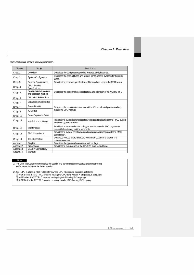
This User Manual contains following information.
Chapter Subject Description
Chap. 1 Overview Describes the configuration, product features, and glossaries.
Chap. 2 System Configuration Describes the product types and system configurations available for the XGR series.
Chap. 3 General Specifications Provides the common specifications of the modules used in the XGR series.
Chap. 4 CPU Module Specifications
Describes the performance, specification, and operation of the XGR-CPUH. Chap. 5 Configuration of program and operation method
Chap. 6 CPU Module Functions
Chap. 7 Expansion driver module
Describes the specifications and use of the I/O module and power module, except the CPU module.
Chap.8 Power Module
Chap. 9 IO Module
Chap. 10 Base Expansion Cable
Chap. 11 Installation and Wiring Provides the guidelines for installation, wiring and precaution of the PLC system to secure system reliability.
Chap. 12 Maintenance Provides the items and methodology of maintenance for PLC system to prevent failure throughout the service life.
Chap. 13 EMC Compliance Provides the system construction and configuration in response to the EMC specification.
Chap. 14 Troubleshooting Describes various errors and faults which may occur in the system and countermeasures..
Append. 1 Flag List Describes the types and contents of various flags. Append. 2 Dimensions Provides the external size of the CPU, I/O module and base. Append. 3 GLOFA Compatibility Append. 4 Warranty
Note 1) This User Manual does not describe the special and communication modules and programming.
Refer related manuals for the information. 2) XGR CPU is a kind of XGT PLC system whose CPU type can be classified as follows; ① XGK Series: the XGT PLC systems having the CPU using Master-K language(LS language) ② XGI Series: the XGT PLC systems having single CPU using IEC language ③ XGR Series: the XGT PLC systems having redundant CPUs using IEC language
Chapter 1. Overview
1-3
1.2 Configuration of the XGR Redundant System XGR Redundancy System provides reliable solution for various types of redundancy systems required in diversified applications. The XGR Redundancy System is economical and user-convenient because the system makes use of the most resources of the XGI system, added with the components for redundancy.
Redundancy
CPU module redundancy Power module redundancy Ethernet communication module redundancy
Modules for redundancy
2 redundant CPUs [optical, electrical] 5 types of power module [standard, large output] – AC110V, AC220V, DC24V individual Redundant bases [2, 6 slots: 2, 6 communication modules can be installed] 3 types of expansion drive modules [per media class: optical, electrical, mixed] Expansion base [12 slots: according to consumption current] 3 types of redundancy expansion drive modules [per media: Optical, electrical, mixed] Redundancy expansion base [12 slots: according to consumption current]
CPU Module
IEC 61131-3 language supported, ladder process rate of 42ns/command, 3MB (Approx. 128kstep) program capacity,
131,072 of I/O points 1Gbps optical communication for CPU synchronization Built-in I/O communication master Provides 2 types of CPU module according to the I/O communication media [optical, electrical]
Redundant system Network •
Expansion drive module Topology: ring [bus type operation activated in case of one error] Provides optical, electrical, and combined media Applied with 100Mbps class industrial Ethernet technology Max. available I/O points: 23,808 (31 stations x 12 slots x 64 points)
Programming Tool Integrated control of all the all XGT types with XG5000 – XGK, XGI, XGB, XGR Convenient programming, various motoring function, diagnosis function, edit funtion Supports various IEC type languages: LD, ST, SFC, IL[Only view function] Supports communication parameter setting, frame monitoring function through XG-PD Supported with software packages per functionalities for motion, APM, temperature controller, etc.
Chapter 1. Overview
1-4
1.3 Features of the XGR Redundancy system XGR Redundancy System provides optimized solutions in various applications with its superb performance and convenience features.
High performance
CPU process rate: 42ns / command High speed backplane Large capacity control points: max. 131,072 points Sufficient program capacity (max. 128ksteps) Sufficient data memory: 25MB Long data type (64bit) and high speed real number operation (single, double) provided Switching operation with minimum delay : if the master CPU fails, operation is switched to the backup CPU within
50ms
Minimum size implemented
Compact panel can be implemented with the minimum size among the class CPU module: Width(55 mm) * Height(98 mm) * Depth(90 mm) Power module
1) XGR-AC12/AC22: Width (55 mm) * Height (98 mm) * Depth (90 mm) 2) XGR-AC13/AC23: Width (55 mm) * Height (98 mm) * Depth (110 mm)
Easy expansion using network Easy installation of expansion bases using network cable Up to 31 remote bases can be added Software program can be uploaded/downloaded via online access from expansion base Communication master module on expansion base enables the installation of smart I/O at anywhere
Improved maintenance maintain ace by system history, network ring configuration, etc. Provides system analysis data including the operation, error, and system histories Network ring configuration enables normal system operation even when a network cable fails Provides network monitoring and protocol monitoring functions If communication fails (smart I/O, etc.), the failed channel can be monitored (by monitoring the flag via HMI). Graphic display of system configuration Module Changing Wizard enables safe replacement of module during operation Base Changing Wizard enables safe replacement of base during operation
IEC 61131-3 (standard language) specification compliance
Provides IEC standard LD, ST, SFC, IL(only view function) Provides IEC standard program structure and data type
Chapter 1. Overview
1-5
Supports various communication functions
Open network enables convenient interface with other products (Ethernet, Profibus, DeviceNet, RS-232C, RS-422/485, etc.)
Supports various protocols for improved convenience Up to 24 communication master modules (12 high speed links, 8 P2Ps) can be mounted on one redundant system. Simple and east network diagnosis using network and communication frame monitoring function RAPIEnet module can be inserted on basic base
Diverse I/O modules are provided for easy system configuration
8, 16, 32, and 64 point modules are provided (8/16 point modules for relay output) Single input, single output, mixed I/O module provided
Extended applications with enhanced analog function
Analog modules can be connected to the slots of all the expansion bases (max. 250 output modules, 139 input modules)
Supports various applications with insulated type analog and temperature module Convenient use by special parameter settings and flags Strengthened debugging function by monitoring flags and data and changing the setting value through special monitor
display window
Provides integrated programming & engineering environments Integrated control of all the all XGT types with XG5000 – XGK, XGI, XGB, XGR Convenient programming, various motoring function, diagnosis function, edit funtion Supports various IEC type languages: LD, ST, SFC, IL[Only view function] Supports communication parameter setting, frame monitoring function through XG-PD Supported with software packages per functionalities for motion, APM, temperature controller, etc.
Provides diversified additional function
Battery backup and flash memory backup for software programs Various restart mode(warm, cold) Task program process Forced ON/OFF of I/O Clock Module changing wizard available during operation Fault mask function Module skip function Extensive operation history supported (system history) Detail error report supported (error history) LED indication of operation status Dot matrix indicator: display operation information and abnormal matters in texts.
PID Function
Max. 256 loops supported Parameter setting using XG5000, convenient monitoring on loop status through Trend monitor Easy control parameter setting using improved auto-tuning function Provides various control modes including normal/reverse combination operation, 2 step SV PID control, cascade
control, etc. Safety secured by diversified alarm functions including PV MAX, PV change, etc.
Chapter 1. Overview
1-6
1.4 Glossary This section provides the major terms and their definitions, used in this Manual.
Terms Definition Remark
Module A standardized component having a specific function to constitute a system. E.g., I/O board designed to be inserted into base.
CPU module, power module, I/O module, etc.
Master CPU Module The CPU module running the present software program. Automatically switched to backup CPU module when the operation is stopped and transfers the control
Standby CPU Module The control function of the master CPU module is transferred to this standby CPU module in case of failure, and this standby CPU module becomes the master CPU module.
Redundant Basic Base
This base can accommodate the CPU module and Ethernet communication module. Master CPU system: the redundant basic system whose CPU module is operating as the master. Standby CPU system: the redundant basic base whose CPU module is operating as backup mode.
Redundant Expansion Base
Expansion base where power module, I/O module, and special/communication module can be installed. (The communication module can be any module except the EtherNet/IP , FEnet and RAPIEnet).
Expansion Drive Module
The module for communication between bases. It also enables setting the base numbers (1~31) with a rotary switch
Synchronous cable 1Gbps optical cable for connection between the CPU modules of a redundant system
CPU redundancy As a part of redundant system, the system is constructed to enable continuous operation when the master CPU module fails using a backup CPU module
Power redundancy A system constructed with redundant power modules to enable continuous system operation when a module of the base fails
Unit A module or a set of module which is the minimum unit of a PLC system operation. A PLC system comprises units and/or sets of units
Basic unit. Expansion unit
PLC System A system consists of PLC and peripheral devices and can be controlled with user software program
XG5000 A programming tool for developing software program, editing and debugging
Module Changing Wizard
A software used for the replacement of CPU module during PLC operation. Power module, I/O module, some of the special modules, and base module can be replaced with this software
Replaceable special modules: A/D,D/A, HSC,RTD
서식 있음: 글꼴: (영어) Arial, (한글) 굴림체, 축소: 0.2pt
Chapter 1. Overview
1-7
Terms Definition Remark
Cold Restart Starting a PLC system and user program after initializing all data (variables and programs such as I/O image area, internal register, timer, counter, etc.) automatically or manually
Warm Restart Along with the function that notifies user-program about power OFF incidents, the user programs are restarted with holding previous data according to setting, after a power OFF.
I/O Image Area The internal memory area of the CPU module installed to maintain I/O status
Cnet Computer Network
FEnet Fast Ethernet Network
Pnet Profibus-DP Network
Dnet DeviceNet Network
Rnet Remote Network
RTC Real Time Clock. The generic IC with a built-in clock function
Watchdog Timer The timer which monitors the preset running time of a user program, and triggers alarm if the process fails to be completed within preset time
Function The operation units which do not store the operation result in the instructions, such as the 4 arithmetical and comparison operations, and output the results of the inputs immediately
Function Block The operation units which store the operation results in the instruction, such as timer and counter, and use the results over multiple scans
Direct Variable The variables used without declaring name and type. For example, I, Q, and M areas are direct variables.
%IX0.0.2 %QW1.2.1 %MD1234, etc.
Automatic Symbolic Variable
The variables used with names and type declared by user. - if declared as‘INPUT_0’=%IX0.0.2, ‘RESULT’=%MD1234, ‘INPUT_0’ and ‘RESULT’ names can be used in the program instead of %IX0.0.2 and %MD1234.
Task The condition for a program start-up, such as fixed cycle task, internal contact point task, and initialization task
Chapter 1. Overview
1-8
Terms Definition Remark
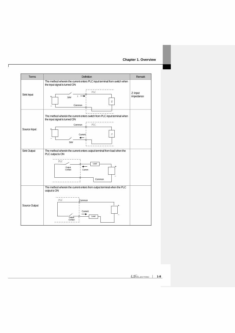
Sink Input
The method wherein the current enters PLC input terminal from switch when the input signal is turned ON
Z: input impedance
Source Input
The method wherein the current enters switch from PLC input terminal when the input signal is turned ON
Sink Output The method wherein the current enters output terminal from load when the PLC output is ON
Source Output
The method wherein the current enters from output terminal when the PLC output is ON
+
− Z
PLC
S/W
Common
Current
+
− Z
PLC
I S/W
Common
+
−
PLC
Current
Output Contact
Common
Load
−
PLC
Current Output Contact
Common
+ Load
Chapter 2. System Configuration
2-1
Chapter 2. System Configuration The XGR Series offer various products for basic systems, computer communication and network systems. This Chapter describes the configuration method and features of each system.
2.1 Product List The product line of the XGR Series is as follows.
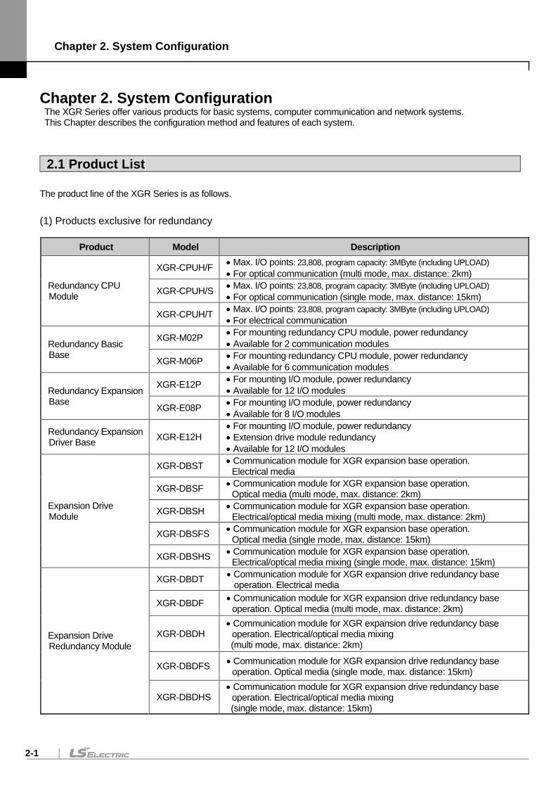
(1) Products exclusive for redundancy
Product Model Description
Redundancy CPU Module
XGR-CPUH/F • Max. I/O points: 23,808, program capacity: 3MByte (including UPLOAD) • For optical communication (multi mode, max. distance: 2km)
XGR-CPUH/S • Max. I/O points: 23,808, program capacity: 3MByte (including UPLOAD) • For optical communication (single mode, max. distance: 15km)
XGR-CPUH/T • Max. I/O points: 23,808, program capacity: 3MByte (including UPLOAD) • For electrical communication
Redundancy Basic Base
XGR-M02P • For mounting redundancy CPU module, power redundancy • Available for 2 communication modules
XGR-M06P • For mounting redundancy CPU module, power redundancy • Available for 6 communication modules
Redundancy Expansion Base
XGR-E12P • For mounting I/O module, power redundancy • Available for 12 I/O modules
XGR-E08P • For mounting I/O module, power redundancy • Available for 8 I/O modules
Redundancy Expansion Driver Base XGR-E12H
• For mounting I/O module, power redundancy • Extension drive module redundancy • Available for 12 I/O modules
Expansion Drive Module
XGR-DBST • Communication module for XGR expansion base operation. Electrical media
XGR-DBSF • Communication module for XGR expansion base operation. Optical media (multi mode, max. distance: 2km)
XGR-DBSH • Communication module for XGR expansion base operation. Electrical/optical media mixing (multi mode, max. distance: 2km)
XGR-DBSFS • Communication module for XGR expansion base operation. Optical media (single mode, max. distance: 15km)
XGR-DBSHS • Communication module for XGR expansion base operation. Electrical/optical media mixing (single mode, max. distance: 15km)
Expansion Drive Redundancy Module
XGR-DBDT • Communication module for XGR expansion drive redundancy base operation. Electrical media
XGR-DBDF • Communication module for XGR expansion drive redundancy base operation. Optical media (multi mode, max. distance: 2km)
XGR-DBDH • Communication module for XGR expansion drive redundancy base
operation. Electrical/optical media mixing (multi mode, max. distance: 2km)
XGR-DBDFS • Communication module for XGR expansion drive redundancy base operation. Optical media (single mode, max. distance: 15km)
XGR-DBDHS • Communication module for XGR expansion drive redundancy base
operation. Electrical/optical media mixing (single mode, max. distance: 15km)
Chapter 2. System Configuration
2-2
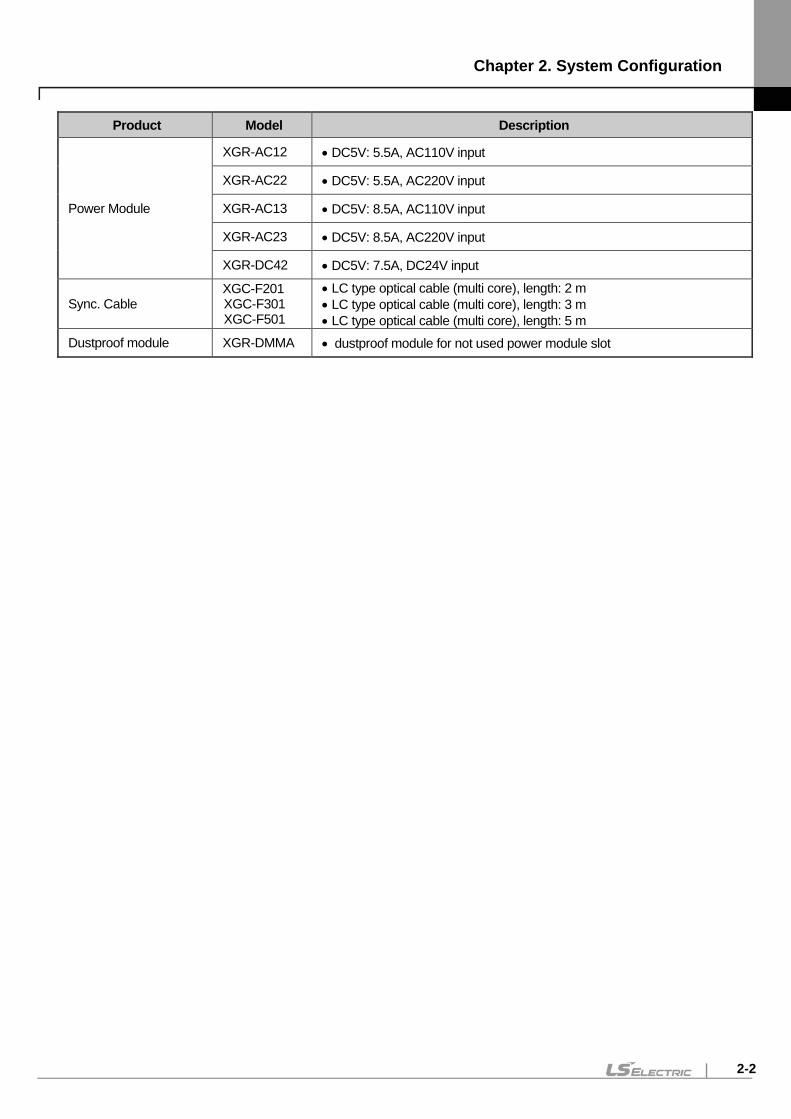
Product Model Description
Power Module
XGR-AC12 • DC5V: 5.5A, AC110V input
XGR-AC22 • DC5V: 5.5A, AC220V input
XGR-AC13 • DC5V: 8.5A, AC110V input
XGR-AC23 • DC5V: 8.5A, AC220V input
XGR-DC42 • DC5V: 7.5A, DC24V input
Sync. Cable XGC-F201 XGC-F301 XGC-F501
• LC type optical cable (multi core), length: 2 m • LC type optical cable (multi core), length: 3 m • LC type optical cable (multi core), length: 5 m
Dustproof module XGR-DMMA • dustproof module for not used power module slot
Chapter 2. System Configuration
2-3
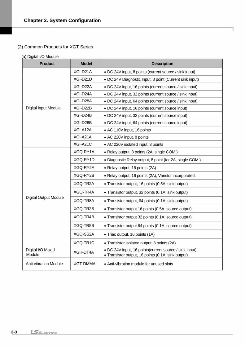
(2) Common Products for XGT Series (a) Digital I/O Module
Product Model Description
Digital Input Module
XGI-D21A • DC 24V input, 8 points (current source / sink input)
XGI-D21D • DC 24V Diagnostic Input, 8 point (Current sink input)
XGI-D22A • DC 24V input, 16 points (current source / sink input)
XGI-D24A • DC 24V input, 32 points (current source / sink input) XGI-D28A • DC 24V input, 64 points (current source / sink input) XGI-D22B • DC 24V input, 16 points (current source input)
XGI-D24B • DC 24V input, 32 points (current source input)
XGI-D28B • DC 24V input, 64 points (current source input)
XGI-A12A • AC 110V input, 16 points
XGI-A21A • AC 220V input, 8 points
XGI-A21C • AC 220V isolated input, 8 points
Digital Output Module
XGQ-RY1A • Relay output, 8 points (2A, single COM.)
XGQ-RY1D • Diagnostic Relay output, 8 point (for 2A, single COM.)
XGQ-RY2A • Relay output, 16 points (2A)
XGQ-RY2B • Relay output, 16 points (2A), Varistor incorporated.
XGQ-TR2A • Transistor output, 16 points (0.5A, sink output)
XGQ-TR4A • Transistor output, 32 points (0.1A, sink output)
XGQ-TR8A • Transistor output, 64 points (0.1A, sink output)
XGQ-TR2B • Transistor output 16 points (0.5A, source output)
XGQ-TR4B • Transistor output 32 points (0.1A, source output)
XGQ-TR8B • Transistor output 64 points (0.1A, source output)
XGQ-SS2A • Triac output, 16 points (1A)
XGQ-TR1C • Transistor isolated output, 8 points (2A) Digital I/O Mixed Module XGH-DT4A • DC 24V input, 16 points(current source / sink input)
• Transistor output, 16 points (0.1A, sink output)
Anti-vibration Module XGT-DMMA • Anti-vibration module for unused slots
Chapter 2. System Configuration
2-4
(b) Process and Motion Control Modules
Product Model Description Remarks
Analog input Module
XGF-AV8A • Voltage Input: 8 channel • DC 1 ~ 5V / 0 ~ 5V / 0 ~ 10V / −10 ~ +10V -
XGF-AC8A • Current Input: 8 channel • DC 4 ~ 20mA / 0 ~ 20mA -
XGF-AD08A • Voltage/Current Input: 8 channels -
XGF-AD4S • Voltage/Current Input: 4 channels • Insulation between channels -
XGF-AD16A • Voltage/Current Input: 16 channels -
XGF-AW4S • 2-wire voltage/current input: 4 –channel, insulation
between channels • 2-wire transmitter driver power supported
-
Analog output Module
XGF-DV4A • Voltage Output: 4 channels • DC 1 ~ 5V / 0 ~ 5V / 0 ~ 10V / −10 ~ +10V -
XGF-DC4A • Current Output:: 4 channels • DC 4 ~ 20mA / 0 ~ 20mA -
XGF-DV4S • Current Output:: 4 channels • Insulation between channels -
XGF-DC4S • Current Output:: 4 channels • Insulation between channels -
XGF-DV8A • Voltage Output: 8 channels • DC 1 ~ 5V / 0 ~ 5V / 0 ~ 10V / −10 ~ +10V -
XGF-DC8A • Current Output:: 8 channels • DC 4 ~ 20mA / 0 ~ 20mA -
Analog I/O Module XGF-AH6A • Voltage/Current input 4 channels
• Voltage/Current output 2 channels -
HART I/F Analog Input
Module XGF-AC4H • Current Input : 4 channel
• HART I/F, DC 4 ~ 20mA -
HART I/F Analog Output
Module XGF-DC4H • Current Output : 4 channel
• HART I/F, DC 4 ~ 20mA -
Thermocouple Input Module XGF-TC4S • Temperature (T/C) Input, 4 channels,
• Insulation between channels -
RTD Input Module
XGF-RD4A • Temperature (RTD) Input, 4 channels -
XGF-RD4S • Temperature (RTD) Input, 4 channels • Insulation between channels -
XGF-RD8A • Temperature (RTD) Input, 8 channels -
Temp. control Module
XGF-TC4UD • Control loop : 4 loops • Input(4 channels, TC/RTD/voltage/current), Output(8 channels, TR/current)
-
XGF-TC4RT • Control loop: 4 loops • input (4 channels, RTD), Output (8 channels, TR) -
High speed Counter Module
XGF-HO2A • Voltage Input type (Open Collector type) • 200kHz, 2 channel -
XGF-HD2A • Differential Input type (Line Driver type) • 500kHz, 2 channel -
XGF-HO8A • Voltage Input type (Open Collector type) • 200kHz, 8 channel -
Chapter 2. System Configuration
2-5
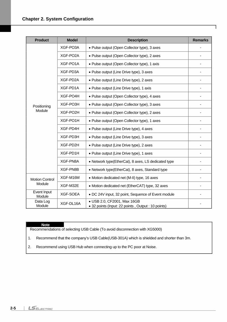
Product Model Description Remarks
Positioning Module
XGF-PO3A • Pulse output (Open Collector type), 3 axes -
XGF-PO2A • Pulse output (Open Collector type), 2 axes -
XGF-PO1A • Pulse output (Open Collector type), 1 axis -
XGF-PD3A • Pulse output (Line Drive type), 3 axes -
XGF-PD2A • Pulse output (Line Drive type), 2 axes -
XGF-PD1A • Pulse output (Line Drive type), 1 axis -
XGF-PO4H • Pulse output (Open Collector type), 4 axes -
XGF-PO3H • Pulse output (Open Collector type), 3 axes -
XGF-PO2H • Pulse output (Open Collector type), 2 axes -
XGF-PO1H • Pulse output (Open Collector type), 1 axes -
XGF-PD4H • Pulse output (Line Drive type), 4 axes -
XGF-PD3H • Pulse output (Line Drive type), 3 axes -
XGF-PD2H • Pulse output (Line Drive type), 2 axes -
XGF-PD1H • Pulse output (Line Drive type), 1 axes -
XGF-PN8A • Network type(EtherCat), 8 axes, LS dedicated type -
XGF-PN8B • Network type(EtherCat), 8 axes, Standard type -
Motion Control Module
XGF-M16M • Motion dedicated net (M-II) type, 16 axes -
XGF-M32E • Motion dedicated net (EtherCAT) type, 32 axes - Event Input
Module XGF-SOEA • DC 24V input, 32 point, Sequence of Event module -
Data Log Module XGF-DL16A • USB 2.0, CF2001, Max 16GB
• 32 points (Input: 22 points , Output : 10 points) -
Note
Recommendations of selecting USB Cable (To avoid disconnection with XG5000)
1. Recommend that the company’s USB Cable(USB-301A) which is shielded and shorter than 3m.
2. Recommend using USB Hub when connecting up to the PC poor at Noise.
Chapter 2. System Configuration
2-6
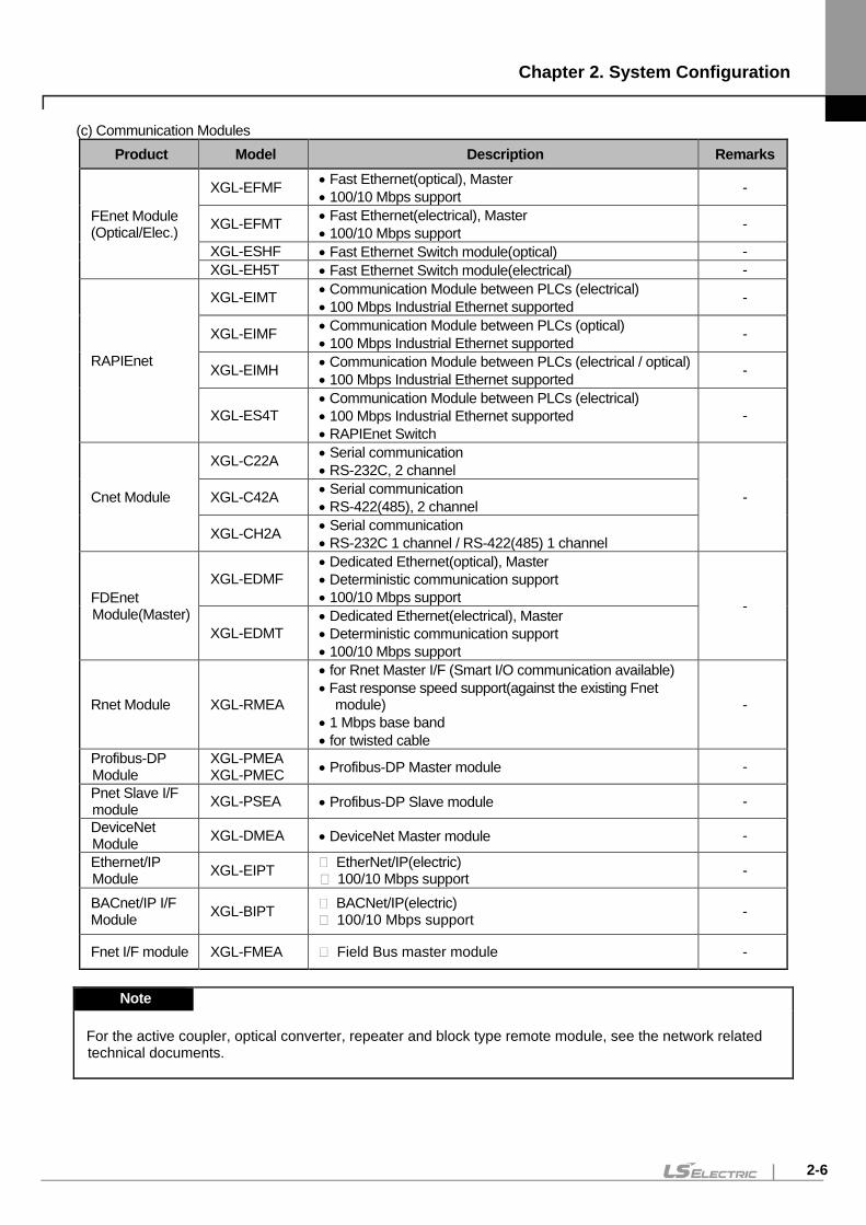
(c) Communication Modules Product Model Description Remarks
FEnet Module (Optical/Elec.)
XGL-EFMF • Fast Ethernet(optical), Master • 100/10 Mbps support -
XGL-EFMT • Fast Ethernet(electrical), Master • 100/10 Mbps support -
XGL-ESHF • Fast Ethernet Switch module(optical) - XGL-EH5T • Fast Ethernet Switch module(electrical) -
RAPIEnet
XGL-EIMT • Communication Module between PLCs (electrical) • 100 Mbps Industrial Ethernet supported -
XGL-EIMF • Communication Module between PLCs (optical) • 100 Mbps Industrial Ethernet supported -
XGL-EIMH • Communication Module between PLCs (electrical / optical) • 100 Mbps Industrial Ethernet supported -
XGL-ES4T • Communication Module between PLCs (electrical) • 100 Mbps Industrial Ethernet supported • RAPIEnet Switch
-
Cnet Module
XGL-C22A • Serial communication • RS-232C, 2 channel
- XGL-C42A • Serial communication • RS-422(485), 2 channel
XGL-CH2A • Serial communication • RS-232C 1 channel / RS-422(485) 1 channel
FDEnet Module(Master)
XGL-EDMF • Dedicated Ethernet(optical), Master • Deterministic communication support • 100/10 Mbps support -
XGL-EDMT • Dedicated Ethernet(electrical), Master • Deterministic communication support • 100/10 Mbps support
Rnet Module XGL-RMEA
• for Rnet Master I/F (Smart I/O communication available) • Fast response speed support(against the existing Fnet
module) • 1 Mbps base band • for twisted cable
-
Profibus-DP Module
XGL-PMEA XGL-PMEC • Profibus-DP Master module -
Pnet Slave I/F module XGL-PSEA • Profibus-DP Slave module -
DeviceNet Module XGL-DMEA • DeviceNet Master module -
Ethernet/IP Module XGL-EIPT EtherNet/IP(electric)
100/10 Mbps support -
BACnet/IP I/F Module XGL-BIPT BACNet/IP(electric)
100/10 Mbps support -
Fnet I/F module XGL-FMEA Field Bus master module -
Note
For the active coupler, optical converter, repeater and block type remote module, see the network related technical documents.
Chapter 2. System Configuration
2-7
2.2 Redundancy System
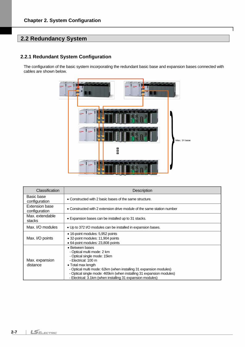
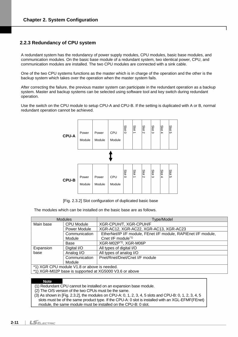
2.2.1 Redundant System Configuration The configuration of the basic system incorporating the redundant basic base and expansion bases connected with cables are shown below.
Classification Description Basic base configuration • Constructed with 2 basic bases of the same structure.
Extension base configuration • Constructed with 2 extension drive module of the same station number
Max. extendable stacks • Expansion bases can be installed up to 31 stacks.
Max. I/O modules • Up to 372 I/O modules can be installed in expansion bases.
Max. I/O points • 16-point modules: 5,952 points • 32-point modules: 11,904 points • 64-point modules: 23,808 points
Max. expansion distance
• Between bases - Optical multi mode: 2 km - Optical single mode: 15km - Electrical: 100 m • Total max length - Optical multi mode: 62km (when installing 31 expansion modules) - Optical single mode: 465km (when installing 31 expansion modules) - Electrical: 3.1km (when installing 31 expansion modules)
Chapter 2. System Configuration
2-8
Classification Description
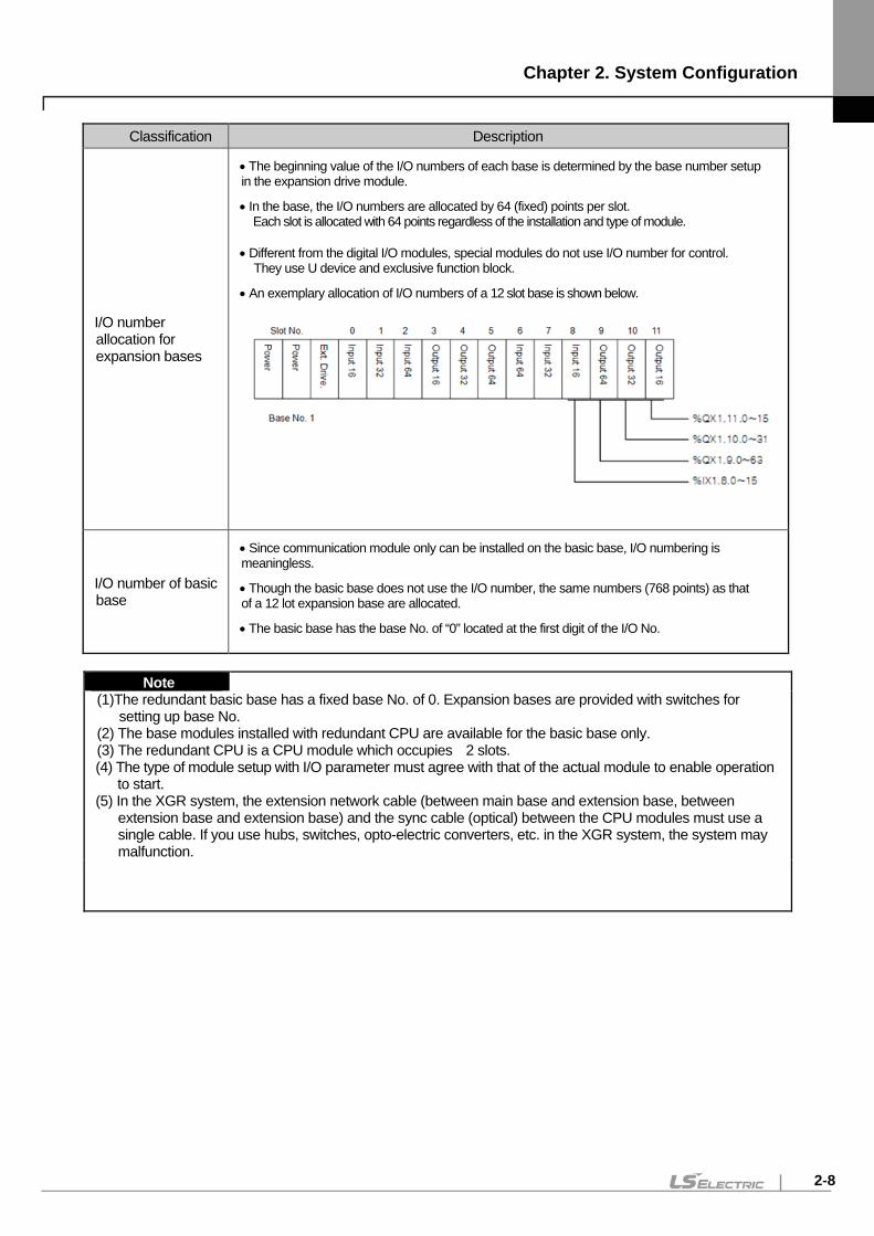
I/O number allocation for expansion bases
• The beginning value of the I/O numbers of each base is determined by the base number setup in the expansion drive module.
• In the base, the I/O numbers are allocated by 64 (fixed) points per slot. Each slot is allocated with 64 points regardless of the installation and type of module.
• Different from the digital I/O modules, special modules do not use I/O number for control.
They use U device and exclusive function block.
• An exemplary allocation of I/O numbers of a 12 slot base is shown below.
I/O number of basic base
• Since communication module only can be installed on the basic base, I/O numbering is meaningless.
• Though the basic base does not use the I/O number, the same numbers (768 points) as that of a 12 lot expansion base are allocated.
• The basic base has the base No. of “0” located at the first digit of the I/O No.
Note
(1)The redundant basic base has a fixed base No. of 0. Expansion bases are provided with switches for setting up base No.
(2) The base modules installed with redundant CPU are available for the basic base only. (3) The redundant CPU is a CPU module which occupies 2 slots. (4) The type of module setup with I/O parameter must agree with that of the actual module to enable operation
to start. (5) In the XGR system, the extension network cable (between main base and extension base, between
extension base and extension base) and the sync cable (optical) between the CPU modules must use a single cable. If you use hubs, switches, opto-electric converters, etc. in the XGR system, the system may malfunction.
Chapter 2. System Configuration
2-9
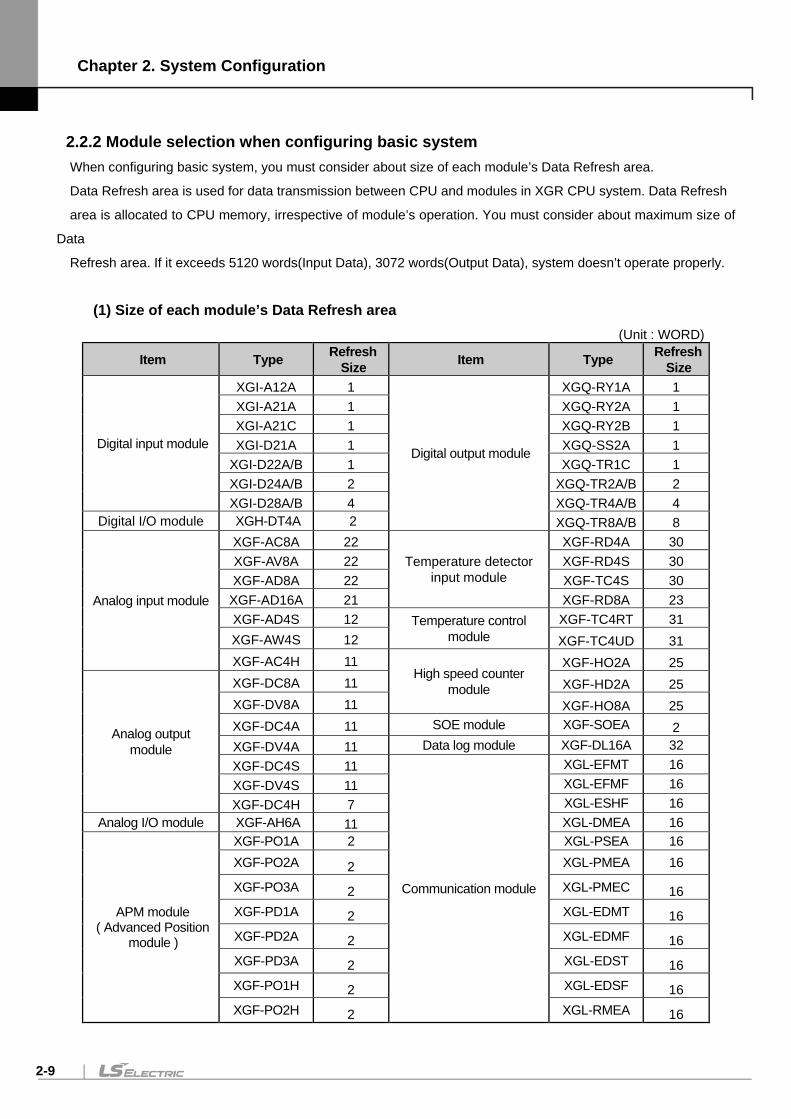
2.2.2 Module selection when configuring basic system When configuring basic system, you must consider about size of each module’s Data Refresh area.
Data Refresh area is used for data transmission between CPU and modules in XGR CPU system. Data Refresh
area is allocated to CPU memory, irrespective of module’s operation. You must consider about maximum size of
Data
Refresh area. If it exceeds 5120 words(Input Data), 3072 words(Output Data), system doesn’t operate properly.
(1) Size of each module’s Data Refresh area (Unit : WORD)
Item Type Refresh Size Item Type Refresh
Size
Digital input module
XGI-A12A 1
Digital output module
XGQ-RY1A 1 XGI-A21A 1 XGQ-RY2A 1 XGI-A21C 1 XGQ-RY2B 1 XGI-D21A 1 XGQ-SS2A 1
XGI-D22A/B 1 XGQ-TR1C 1 XGI-D24A/B 2 XGQ-TR2A/B 2 XGI-D28A/B 4 XGQ-TR4A/B 4
Digital I/O module XGH-DT4A 2 XGQ-TR8A/B 8
Analog input module
XGF-AC8A 22 Temperature detector
input module
XGF-RD4A 30 XGF-AV8A 22 XGF-RD4S 30 XGF-AD8A 22 XGF-TC4S 30
XGF-AD16A 21 XGF-RD8A 23 XGF-AD4S 12 Temperature control
module XGF-TC4RT 31
XGF-AW4S 12 XGF-TC4UD 31 XGF-AC4H 11
High speed counter module
XGF-HO2A 25
Analog output module
XGF-DC8A 11 XGF-HD2A 25 XGF-DV8A 11 XGF-HO8A 25 XGF-DC4A 11 SOE module XGF-SOEA 2 XGF-DV4A 11 Data log module XGF-DL16A 32 XGF-DC4S 11
Communication module
XGL-EFMT 16 XGF-DV4S 11 XGL-EFMF 16 XGF-DC4H 7 XGL-ESHF 16
Analog I/O module XGF-AH6A 11 XGL-DMEA 16
APM module ( Advanced Position
module )
XGF-PO1A 2 XGL-PSEA 16 XGF-PO2A 2 XGL-PMEA 16
XGF-PO3A 2 XGL-PMEC 16 XGF-PD1A 2 XGL-EDMT 16 XGF-PD2A 2 XGL-EDMF 16 XGF-PD3A 2 XGL-EDST 16 XGF-PO1H 2 XGL-EDSF 16 XGF-PO2H 2 XGL-RMEA 16
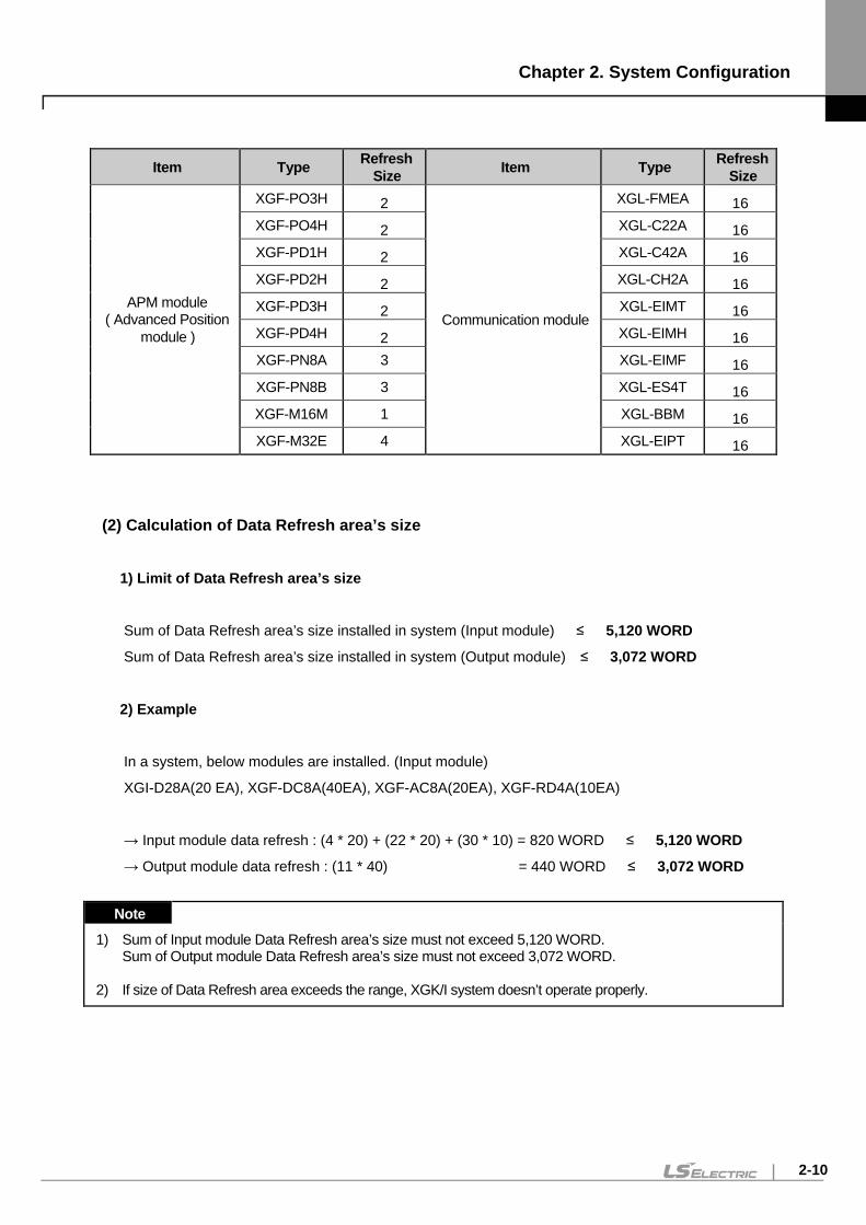
Chapter 2. System Configuration
2-10
Item Type Refresh Size Item Type Refresh
Size
APM module ( Advanced Position
module )
XGF-PO3H 2
Communication module
XGL-FMEA 16 XGF-PO4H 2 XGL-C22A 16 XGF-PD1H 2 XGL-C42A 16 XGF-PD2H 2 XGL-CH2A 16 XGF-PD3H 2 XGL-EIMT 16 XGF-PD4H 2 XGL-EIMH 16 XGF-PN8A 3 XGL-EIMF 16 XGF-PN8B 3 XGL-ES4T 16 XGF-M16M 1 XGL-BBM 16 XGF-M32E 4 XGL-EIPT 16
(2) Calculation of Data Refresh area’s size
1) Limit of Data Refresh area’s size
Sum of Data Refresh area’s size installed in system (Input module) ≤ 5,120 WORD
Sum of Data Refresh area’s size installed in system (Output module) ≤ 3,072 WORD
2) Example In a system, below modules are installed. (Input module)
XGI-D28A(20 EA), XGF-DC8A(40EA), XGF-AC8A(20EA), XGF-RD4A(10EA)
→ Input module data refresh : (4 * 20) + (22 * 20) + (30 * 10) = 820 WORD ≤ 5,120 WORD
→ Output module data refresh : (11 * 40) = 440 WORD ≤ 3,072 WORD
Note
1) Sum of Input module Data Refresh area’s size must not exceed 5,120 WORD. Sum of Output module Data Refresh area’s size must not exceed 3,072 WORD.
2) If size of Data Refresh area exceeds the range, XGK/I system doesn’t operate properly.
Chapter 2. System Configuration
2-11
2.2.3 Redundancy of CPU system
A redundant system has the redundancy of power supply modules, CPU modules, basic base modules, and communication modules. On the basic base module of a redundant system, two identical power, CPU, and communication modules are installed. The two CPU modules are connected with a sink cable. One of the two CPU systems functions as the master which is in charge of the operation and the other is the backup system which takes over the operation when the master system fails. After correcting the failure, the previous master system can participate in the redundant operation as a backup system. Master and backup systems can be selected using software tool and key switch during redundant operation. Use the switch on the CPU module to setup CPU-A and CPU-B. If the setting is duplicated with A or B, normal redundant operation cannot be achieved.
CPU-A Power
Module
Power
Module
CPU
Module
Slot 0
Slot 1
Slot 2
Slot 3
Slot 4
Slot 5
CPU-B Power
Module
Power
Module
CPU
Module
Slot 0
Slot 1
Slot 2
Slot 3
Slot 4
Slot 5
[Fig. 2.3.2] Slot configuration of duplicated basic base
The modules which can be installed on the basic base are as follows.
Modules Type/Model Main base CPU Module XGR-CPUH/T, XGR-CPUH/F
Power Module XGR-AC12, XGR-AC22, XGR-AC13, XGR-AC23 Communication Module
EtherNet/IP I/F module, FEnet I/F module, RAPIEnet I/F module, Cnet I/F module*1)
Base XGR-M02P*2), XGR-M06P Expansion base
Digital I/O All types of digital I/O Analog I/O All types of analog I/O Communication Module
Pnet/Rnet/Dnet/Cnet I/F module
*1) XGR CPU module V1.8 or above is needed. *1) XGR-M02P base is supported at XG5000 V3.6 or above
Note
(1) Redundant CPU cannot be installed on an expansion base module. (2) The O/S version of the two CPUs must be the same. (3) As shown in [Fig. 2.3.2], the modules on CPU-A: 0, 1, 2, 3, 4, 5 slots and CPU-B: 0, 1, 2, 3, 4, 5
slots must be of the same product type. If the CPU-A: 0 slot is installed with an XGL-EFMF(FEnet) module, the same module must be installed on the CPU-B: 0 slot.
Chapter 2. System Configuration
2-12
2.2.4 Power Module Redundancy
The power modules of the basic and expansion base systems can have a redundancy.
The redundant power module enables continuous system operation without interruption when one of the two
power modules fails to supply power.
Power system or power module failure can be repaired or the module can be replaced during operation without
interruption. 2.2.5 Extension Drive Redundancy Extension redundancy system consists of power module, extension drive module, redundancy extension base, redundancy cable. All modules except extension base modules are backed up by redundancy. One extension driver operates as master system and another operation as standby which gets the right when error occurs at master system. Master extension driver recovered from error gets stand-by and doesn’t participate in an operation. When changing extension drive module during RUN mode, use “Base Skip”.
Extension redundancy drive modules in the same extension base should have same station number. Extension redundancy drive module has to be mounted on the designated position of extension base
Master-standby status of extension driver is determined by operating status of CPU.
2.2.6 Expansion Base Communication Path Redundancy
Since the cable connection of the expansion bases are ring-structured, the system can be operated without
interruption even when a cable fails, by using the other cable.
In normal ring operation mode, operation is performed using the path which is nearer to the master. When a
cable fails, the system operation is maintained by line operation mode.
The failed cable can be replaced without interrupting the operation.
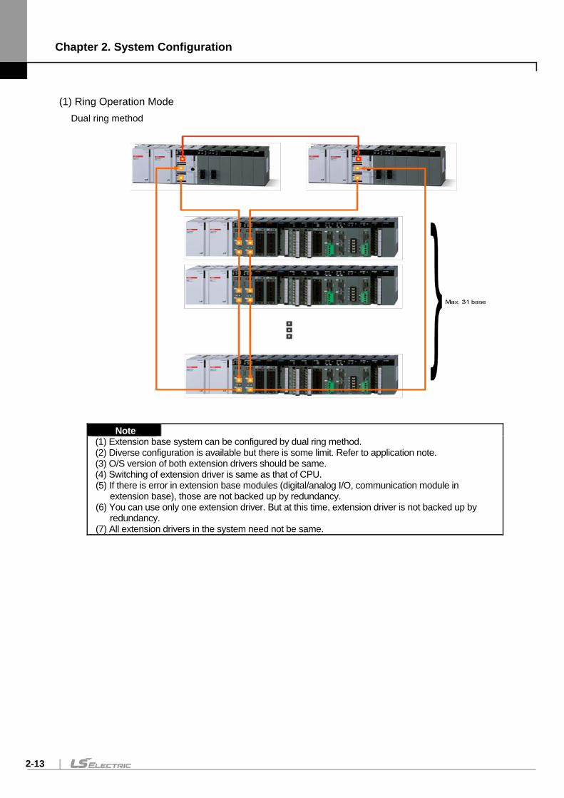
Chapter 2. System Configuration
2-13
(1) Ring Operation Mode Dual ring method
Note (1) Extension base system can be configured by dual ring method. (2) Diverse configuration is available but there is some limit. Refer to application note. (3) O/S version of both extension drivers should be same. (4) Switching of extension driver is same as that of CPU. (5) If there is error in extension base modules (digital/analog I/O, communication module in
extension base), those are not backed up by redundancy. (6) You can use only one extension driver. But at this time, extension driver is not backed up by
redundancy. (7) All extension drivers in the system need not be same.
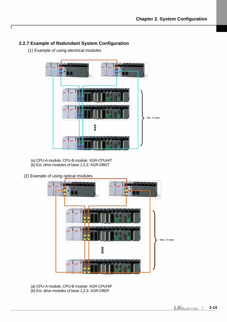
Chapter 2. System Configuration
2-14
2.2.7 Example of Redundant System Configuration
(1) Example of using electrical modules
(a) CPU-A module, CPU-B module: XGR-CPUH/T (b) Ext. drive modules of base 1,2,3: XGR-DBDT
(2) Example of using optical modules
(a) CPU-A module, CPU-B module: XGR-CPUH/F (b) Ext. drive modules of base 1,2,3: XGR-DBDF
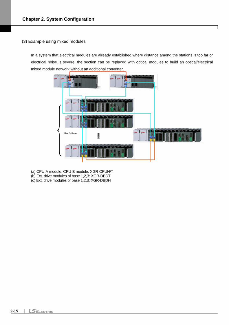
Chapter 2. System Configuration
2-15
(3) Example using mixed modules
In a system that electrical modules are already established where distance among the stations is too far or
electrical noise is severe, the section can be replaced with optical modules to build an optical/electrical
mixed module network without an additional converter.
(a) CPU-A module, CPU-B module: XGR-CPUH/T (b) Ext. drive modules of base 1,2,3: XGR-DBDT (c) Ext. drive modules of base 1,2,3: XGR-DBDH
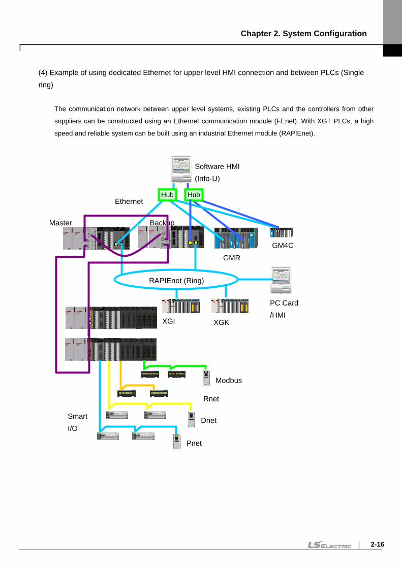
Chapter 2. System Configuration
2-16
(4) Example of using dedicated Ethernet for upper level HMI connection and between PLCs (Single ring)
The communication network between upper level systems, existing PLCs and the controllers from other
suppliers can be constructed using an Ethernet communication module (FEnet). With XGT PLCs, a high
speed and reliable system can be built using an industrial Ethernet module (RAPIEnet).
RAPIEnet (Ring)
GMR
PC Card /HMI
Master Backup
Ethernet
XGK
Smart I/O
Software HMI (Info-U)
Hub
Modbus
Pnet
Dnet
Rnet
Hub
XGI
GM4C
Chapter 2. System Configuration
2-17
2.3 Network System XGR Series support diversified network systems for flexible system configuration methodology. For the communication between PLCs and upper level systems or between PLCs, Ethernet (EthNet/IP, FEnet, RAPIEnet) and Cnet are provided. For lower control network system, Profibus-DP, DeviceNet, and Rnet are provided.
2.3.1 Networking among Systems Only EthNet/IP , FEnet and RAPIEnet communication modules are available for the redundant basic base. All communication modules except Ethernet communication module can be installed in the expansion base. Maximum 24 communication modules can be installed in the redundant basic base and expansion bases. Maximum number of modules limited by functionality are as follows;
Functionality Maximum No. of Modules
Max. No. of modules for high speed link configuration 12
Max. No. of P2P1) service modules 8
Max. No. of dedicated service (slave) modules 24
*Note1) : P2Pservice: 1 to 1 communication
2.3.2 Remote I/O System
For the control network systems of the I/O modules distributed across remote locations, Profibus-DP, DeviceNet, Rnet, Cnet, etc., are provided.
(1) I/O System Application by Network Type Remote I/O modules are classified into base board type and block type (Smart I/O, etc.). Base board type may not be supported in certain network types.
No. Network Type (Master)
Block-type Remote I/O (Smart IO)
Ext.-type Remote I/O
1 Profibus-DP O O
2 DeviceNet O O
3 Rnet O O
4 Cnet(MODBUS) O - * The above specifications can be changed for functional improvement. Please refer to the technical material of the network system for detail information.
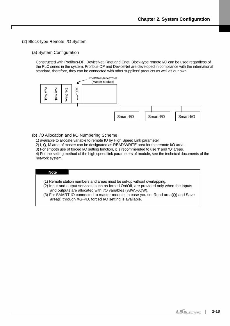
Chapter 2. System Configuration
2-18
(2) Block-type Remote I/O System
(a) System Configuration Constructed with Profibus-DP, DeviceNet, Rnet and Cnet. Block-type remote I/O can be used regardless of the PLC series in the system. Profibus-DP and DeviceNet are developed in compliance with the international standard, therefore, they can be connected with other suppliers’ products as well as our own.
(b) I/O Allocation and I/O Numbering Scheme 1) available to allocate variable to remote IO by High Speed Link parameter 2) I, Q, M area of master can be designated as READ/WRITE area for the remote I/O area. 3) For smooth use of forced I/O setting function, it is recommended to use ‘I’ and ‘Q’ areas. 4) For the setting method of the high speed link parameters of module, see the technical documents of the network system.
Note
(1) Remote station numbers and areas must be set-up without overlapping.
(2) Input and output services, such as forced On/Off, are provided only when the inputs and outputs are allocated with I/O variables (%IW,%QW).
(3) For SMART IO connected to master module, in case you set Read area(Q) and Save area(I) through XG-PD, forced I/O setting is available.
Pwr/ M
od.
Pwr/ M
od.
Ext. Drive.
Pnet/Dnet/Rnet/Cnet (Master Module)
Smart-I/O Smart-I/O Smart-I/O
XGL−****
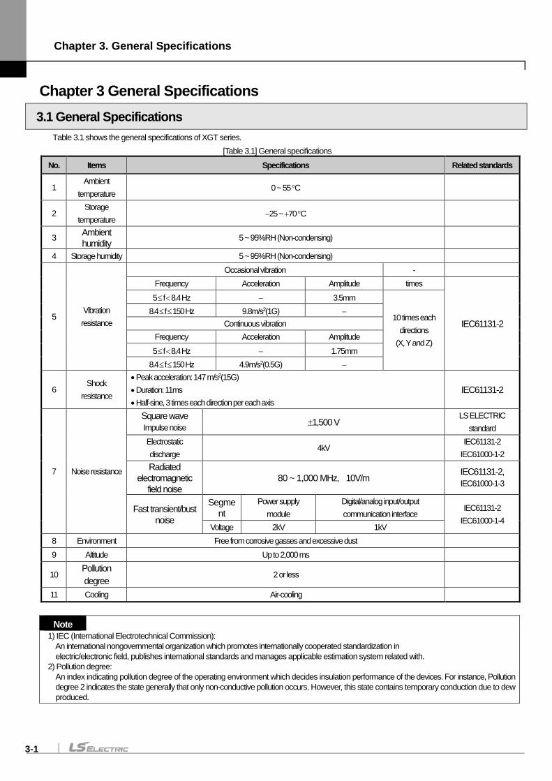
Chapter 3. General Specifications
3-1
Chapter 3 General Specifications 3.1 General Specifications
Table 3.1 shows the general specifications of XGT series. [Table 3.1] General specifications
No. Items Specifications Related standards
1 Ambient
temperature 0 ~ 55 °C
2 Storage
temperature −25 ~ +70 °C
3 Ambient humidity 5 ~ 95%RH (Non-condensing)
4 Storage humidity 5 ~ 95%RH (Non-condensing)
5 Vibration resistance
Occasional vibration - Frequency Acceleration Amplitude times
IEC61131-2
5 ≤ f < 8.4 Hz − 3.5mm
10 times each directions
(X, Y and Z)
8.4 ≤ f ≤ 150 Hz 9.8m/s2(1G) − Continuous vibration
Frequency Acceleration Amplitude
5 ≤ f < 8.4 Hz − 1.75mm 8.4 ≤ f ≤ 150 Hz 4.9m/s2(0.5G) −
6 Shock
resistance
• Peak acceleration: 147 m/s2(15G) • Duration: 11ms • Half-sine, 3 times each direction per each axis
IEC61131-2
7 Noise resistance
Square wave Impulse noise ±1,500 V
LS ELECTRIC standard
Electrostatic discharge
4kV IEC61131-2
IEC61000-1-2 Radiated
electromagnetic field noise
80 ~ 1,000 MHz, 10V/m IEC61131-2, IEC61000-1-3
Fast transient/bust noise
Segment
Power supply module
Digital/analog input/output communication interface
IEC61131-2 IEC61000-1-4
Voltage 2kV 1kV 8 Environment Free from corrosive gasses and excessive dust 9 Altitude Up to 2,000 ms
10 Pollution degree
2 or less
11 Cooling Air-cooling
Note
1) IEC (International Electrotechnical Commission): An international nongovernmental organization which promotes internationally cooperated standardization in
electric/electronic field, publishes international standards and manages applicable estimation system related with. 2) Pollution degree:
An index indicating pollution degree of the operating environment which decides insulation performance of the devices. For instance, Pollution degree 2 indicates the state generally that only non-conductive pollution occurs. However, this state contains temporary conduction due to dew produced.

Chapter 3. General Specifications
3-2
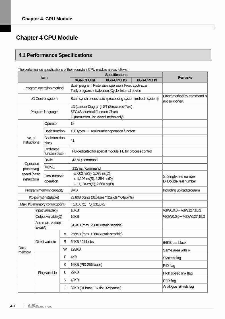
Chapter 4. CPU Module
4-1
Chapter 4 CPU Module
4.1 Performance Specifications The performance specifications of the redundant CPU module are as follows.
Item Specifications Remarks XGR-CPUH/F XGR-CPUH/S XGR-CPUH/T
Program operation method Scan program: Reiterative operation, Fixed cycle scan Task program: Initialization, Cycle, Internal device
I/O Control system Scan synchronous batch processing system (refresh system). Direct method by command is not supported.
Program language LD (Ladder Diagram), ST (Structured Text) SFC (Sequential Function Chart) IL (Instruction List, view function only)
No. of Instructions
Operator 18
Basic function 130 types + real number operation function
Basic function block 41
Dedicated function block FB dedicated for special module, FB for process control
Operation processing
speed (basic instruction)
Basic 42 ns / command
MOVE 112 ns / command
Real number operation
±: 602 ns(S), 1,078 ns(D) x: 1,106 ns(S), 2,394 ns(D) ÷ : 1,134 ns(S), 2,660 ns(D)
S: Single real number D: Double real number
Program memory capacity 3MB Including upload program
I/O points(installable) 23,808 points (31bases * 12slots * 64points)
Max. I/O memory contact point I: 131,072, Q: 131,072
Data memory
Input variable(I) 16KB %IW0.0.0 ~ %IW127.15.3 Output variable(Q) 16KB %QW0.0.0 ~ %QW127.15.3 Automatic variable area(A) 512KB (max. 256KB retain settable)
Direct variable
M 256KB (max. 128KB retain settable)
R 64KB * 2 blocks 64KB per block
W 128KB Same area with R
Flag variable
F 4KB System flag
K 16KB (PID 256 loops) PID flag
L 22KB High speed link flag
N 42KB P2P flag
U 32KB (31 base, 16 slot, 32channel) Analogue refresh flag
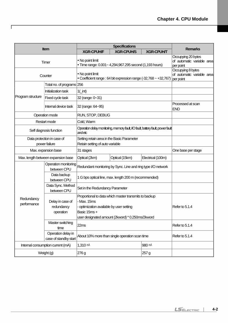
Chapter 4. CPU Module
4-2
Item Specifications Remarks XGR-CPUH/F XGR-CPUH/S XGR-CPUH/T
Timer No point limit Time range: 0.001~ 4,294,967.295 second (1,193 hours)
Occupying 20 bytes of automatic variable area per point
Counter No point limit Coefficient range : 64 bit expression range (-32,768 ~ +32,767)
Occupying 8 bytes of automatic variable area per point
Program structure
Total no. of programs 256
Initialization task 1(_int)
Fixed cycle task 32 (range: 0~31)
Internal device task 32 (range: 64~95) Processed at scan END
Operation mode RUN, STOP, DEBUG
Restart mode Cold, Warm
Self diagnosis function Operation delay monitoring, memory fault, I/O fault, battery fault, power fault and etc
Data protection in case of power failure
Setting retain area in the Basic Parameter Retain setting of auto variable
Max. expansion base 31 stages One base per stage
Max. length between expansion base Optical (2km) Optical (15km) Electrical (100m)
Redundancy performance
Operation monitoring between CPU
Redundant monitoring by Sync. Line and ring type I/O network
Data backup between CPU
1 G bps optical line, max. length 200 m (recommended)
Data Sync. Method between CPU
Set in the Redundancy Parameter
Delay in case of redundancy operation
Proportional to data which master transmits to backup - Max. 15ms - optimization available by user setting Basic 15ms + user designated amount (2kword) * 0.250ms/2kword
Refer to 5.1.4
Master switching time
22ms Refer to 5.1.4
Operation delay in case of standby start
About 10% more than single operation scan time Refer to 5.1.4
Internal consumption current (mA) 1,310 980
Weight (g) 276 g 257 g
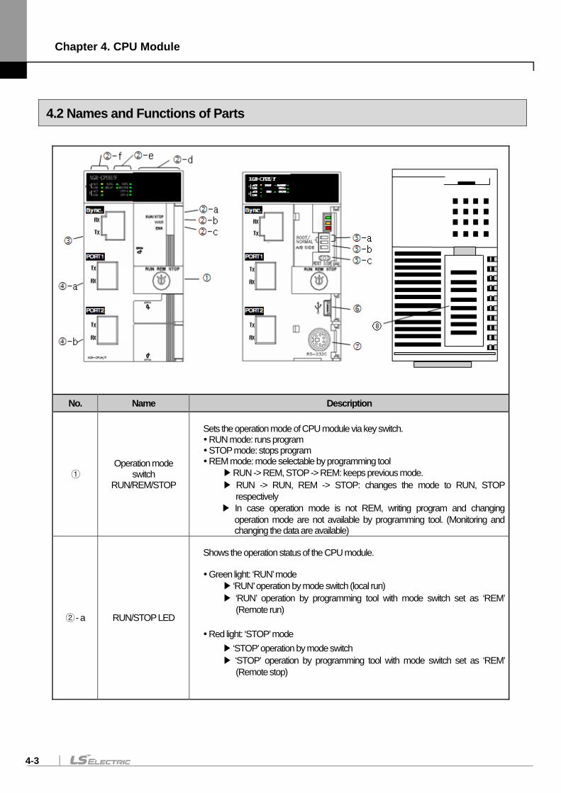
Chapter 4. CPU Module
4-3
4.2 Names and Functions of Parts
No. Name Description
① Operation mode
switch RUN/REM/STOP
Sets the operation mode of CPU module via key switch. RUN mode: runs program STOP mode: stops program REM mode: mode selectable by programming tool RUN -> REM, STOP -> REM: keeps previous mode. RUN -> RUN, REM -> STOP: changes the mode to RUN, STOP
respectively In case operation mode is not REM, writing program and changing
operation mode are not available by programming tool. (Monitoring and changing the data are available)
② - a RUN/STOP LED
Shows the operation status of the CPU module. Green light: ‘RUN’ mode ‘RUN’ operation by mode switch (local run) ‘RUN’ operation by programming tool with mode switch set as ‘REM’
(Remote run) Red light: ‘STOP’ mode ‘STOP’ operation by mode switch ‘STOP’ operation by programming tool with mode switch set as ‘REM’
(Remote stop)
Chapter 4. CPU Module
4-4
No. Name Description
② - b WAR. LED
On(yellow): displaying an warning
Force I/O setting Skip I/O/Fault mask setting Run when Fuse error Run when I/O module error Run when special module error Run when communication module error Warning abnormal RTC data Warning existence of base which doesn’t participate in the operation Abnormal operation stop warning Task collision warning Abnormal battery warning Warning detection of light error of external device High speed link setting warning P2P setting warning Fixed cycle error warning Abnormal base power module warning Abnormal base skip cancellation warning Abnormal base number setting warning Warning redundant configuration Warning OS version inconsistency Warning Ring topology configuration
Off: No warning
② - c ERR. LED
On(red): displays error makes the operation unavailable
CPU configuration error Module type mismatch error Module detached error Fuse disconnection error Detection of heavy trouble of external device Basic parameter error I/O parameter error Special module parameter error User program error Program code error CPU abnormal end or malfunction Base power error Scan watchdog error Base information error Standby CPU run error Expansion base detached error Redundant parameter error Module insertion location error Expansion base no. overlapped error Redundant Sync. Error A/B side overlapped setting error Base abnormal configuration error
Off: No error
Chapter 4. CPU Module
4-5
No. Name Description
② - d Displaying operation status
Displays operation status with 4 characters Normal operation
Warning Error (Refer to XGR error code)
② - e Displaying redundancy status
Displays operation/installation status of CPU system.
RED: On when redundant operation, Off when single operation MASTER: on; CPU operating as master, off; standby CPU CPU-A: on when CPU position designation switch (⑤-b) set as A CPU-B: on when CPU position designation switch (⑤-b) set as B
② - f Displaying expansion network status
Displays communication status with expansion base ACT On (yellow): relevant channel is operating LINK On (Green): link of relevant channel is connected
1 indicates upper channel (④-a), 2 indicates lower channel (④-b). RING On (Green): Expansion network is configured as Ring. Ring Off: Expansion network is not established or configured as Line because part
of Ring fails
③ Sync. connector Data sharing and monitoring between two CPUS.
④-a ④-b
Connector for expansion connector
Connector used for connecting with expansion base For easy Ring configuration, two connector supported Two types, optical/optical, electrical/electrical
⑤-a BOOT/NORMAL switch
Used to download OS at first time BOOT/NORMAL (right side): used for normal operation BOOT/NORMAL (left side): used to download OS (OS download mode).
⑤-b A/B side switch (CPU position
designation switch)
Designates the logical position of CPU Left side means CPU position is set as A Right side means CPU position is set as B Two CPU should have a different position. (available to check in the programming tool) In case two PLC are set as same position, the lately started one cause “E101” error
(1) BOOT/NORMAL switch always should be set to right side. (2) In case of setting to left side, system doesn’t operate properly and
It is not allowed for the user to use (3) BOOT/NORMAL switch is not allowed to set to left side for OS downloading
Caution
Chapter 4. CPU Module
4-6
No. Name Description
⑤-c Reset/D. Clear switch
You can enable/disable Reset/D.Clear switch in “XG5000 Basic Parameter Basic Operation Setup” 1. When Reset switch is enabled
Operation Result move to left return to center Reset move to left keep 3 seconds or above return to center
Overall reset
2. When D.Clear switch is enabled
Operation Result move to right return to center: General data area and retain area (M,
Automatic variable) will be cleared. move to left keep 3 seconds or above return to center:
General data area, retain area (M, Automatic variable) and R area will be cleared.
⑥ USB connector Connector for connecting with peripheral (XG5000 etc.) (supports USB 1.1)
⑦ RS-232C connector Connector for connecting with peripheral (XG5000 etc.)
⑧ Backup battery cover Backup battery cover
(1) Data clear function is only executed in stop mode.
Caution
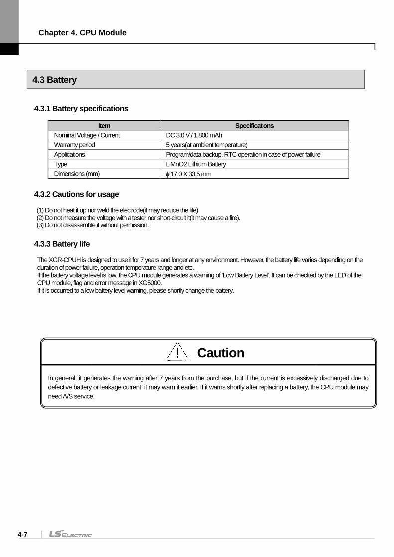
Chapter 4. CPU Module
4-7
4.3 Battery
4.3.1 Battery specifications
Item Specifications Nominal Voltage / Current DC 3.0 V / 1,800 mAh Warranty period 5 years(at ambient temperature) Applications Program/data backup, RTC operation in case of power failure Type LiMnO2 Lithium Battery Dimensions (mm) φ 17.0 X 33.5 mm
4.3.2 Cautions for usage (1) Do not heat it up nor weld the electrode(it may reduce the life) (2) Do not measure the voltage with a tester nor short-circuit it(it may cause a fire). (3) Do not disassemble it without permission.
4.3.3 Battery life The XGR-CPUH is designed to use it for 7 years and longer at any environment. However, the battery life varies depending on the duration of power failure, operation temperature range and etc. If the battery voltage level is low, the CPU module generates a warning of ‘Low Battery Level’. It can be checked by the LED of the CPU module, flag and error message in XG5000. If it is occurred to a low battery level warning, please shortly change the battery.
In general, it generates the warning after 7 years from the purchase, but if the current is excessively discharged due to defective battery or leakage current, it may warn it earlier. If it warns shortly after replacing a battery, the CPU module may need A/S service.
Caution
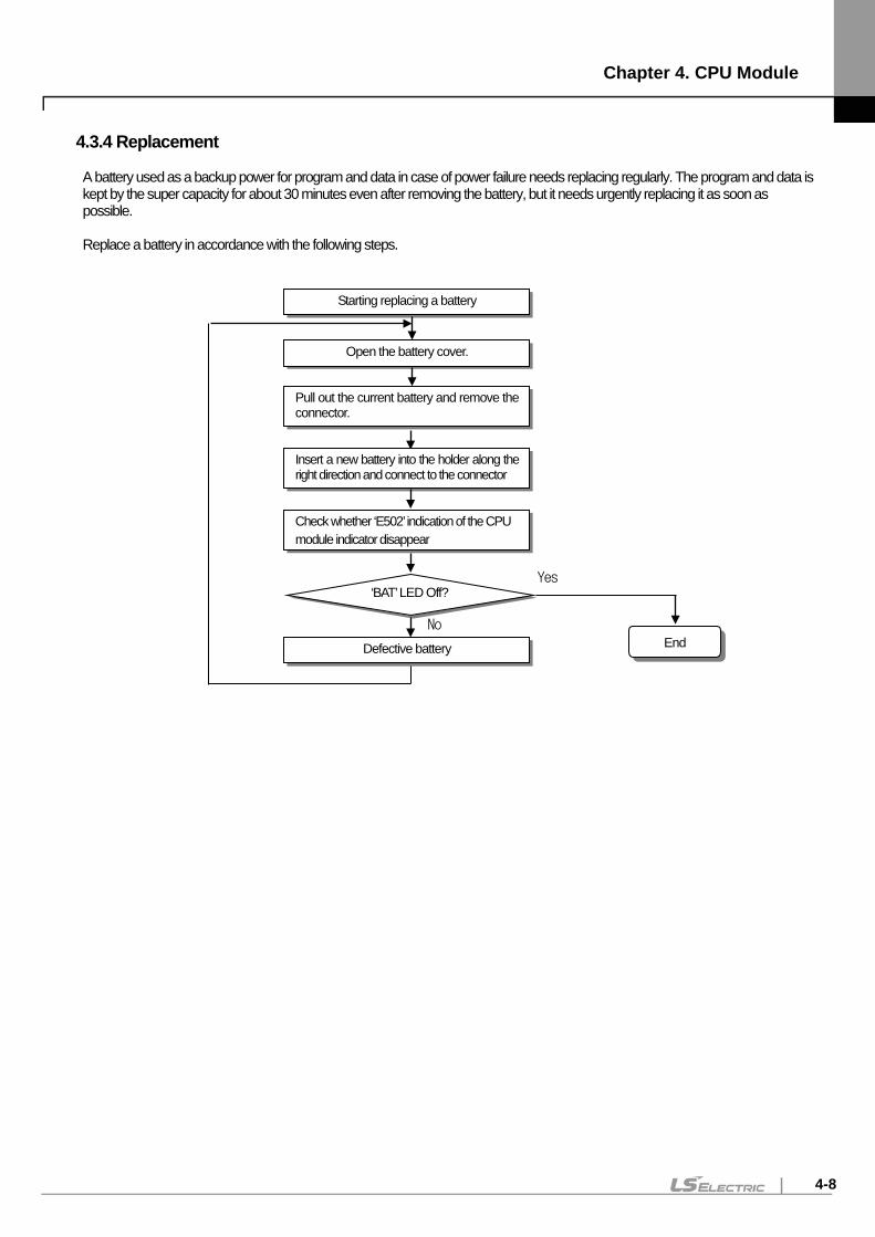
Chapter 4. CPU Module
4-8
4.3.4 Replacement A battery used as a backup power for program and data in case of power failure needs replacing regularly. The program and data is kept by the super capacity for about 30 minutes even after removing the battery, but it needs urgently replacing it as soon as possible. Replace a battery in accordance with the following steps.
Starting replacing a battery
Open the battery cover.
Pull out the current battery and remove the connector.
Insert a new battery into the holder along the right direction and connect to the connector
Check whether ‘E502’ indication of the CPU module indicator disappear
‘BAT’ LED Off?
Defective battery
No
Yes
End
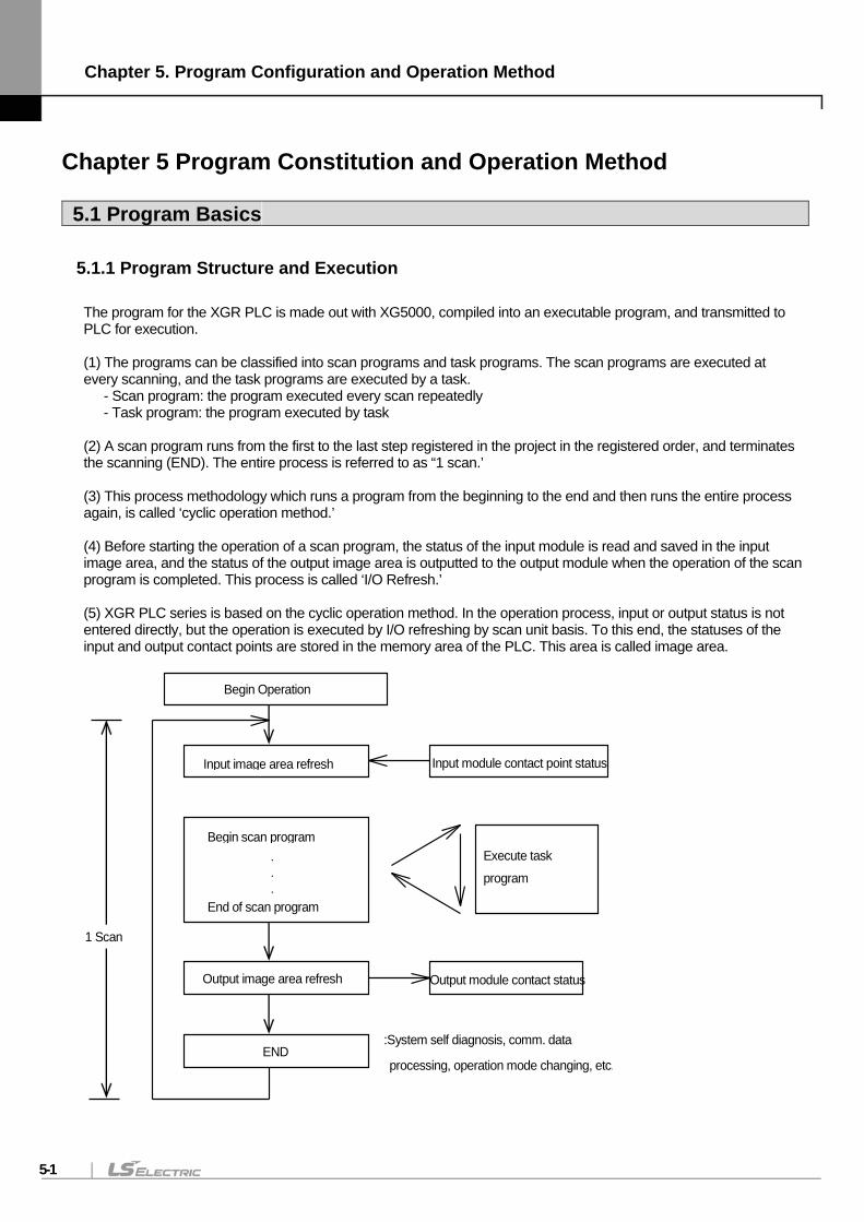
Chapter 5. Program Configuration and Operation Method
5-1
Chapter 5 Program Constitution and Operation Method
5.1 Program Basics
5.1.1 Program Structure and Execution
The program for the XGR PLC is made out with XG5000, compiled into an executable program, and transmitted to PLC for execution. (1) The programs can be classified into scan programs and task programs. The scan programs are executed at every scanning, and the task programs are executed by a task. - Scan program: the program executed every scan repeatedly - Task program: the program executed by task (2) A scan program runs from the first to the last step registered in the project in the registered order, and terminates the scanning (END). The entire process is referred to as “1 scan.’ (3) This process methodology which runs a program from the beginning to the end and then runs the entire process again, is called ‘cyclic operation method.’ (4) Before starting the operation of a scan program, the status of the input module is read and saved in the input image area, and the status of the output image area is outputted to the output module when the operation of the scan program is completed. This process is called ‘I/O Refresh.’ (5) XGR PLC series is based on the cyclic operation method. In the operation process, input or output status is not entered directly, but the operation is executed by I/O refreshing by scan unit basis. To this end, the statuses of the input and output contact points are stored in the memory area of the PLC. This area is called image area. Begin Operation
Input image area refresh
Begin scan program
End of scan program
Output image area refresh
END
1 Scan
.
.
.
Input module contact point status
Output module contact status
Execute task program
:System self diagnosis, comm. data
processing, operation mode changing, etc.
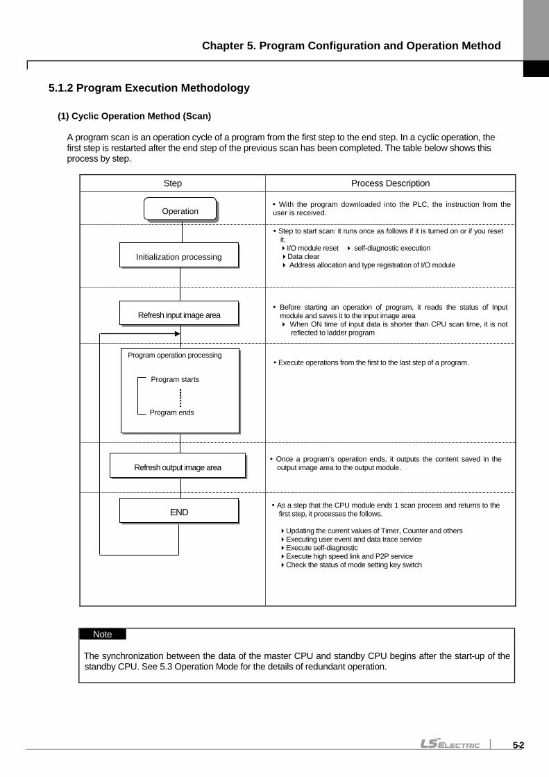
Chapter 5. Program Configuration and Operation Method
5-2
5.1.2 Program Execution Methodology
(1) Cyclic Operation Method (Scan) A program scan is an operation cycle of a program from the first step to the end step. In a cyclic operation, the first step is restarted after the end step of the previous scan has been completed. The table below shows this process by step.
Step Process Description
With the program downloaded into the PLC, the instruction from the user is received.
Note The synchronization between the data of the master CPU and standby CPU begins after the start-up of the standby CPU. See 5.3 Operation Mode for the details of redundant operation.
As a step that the CPU module ends 1 scan process and returns to the
first step, it processes the follows. Updating the current values of Timer, Counter and others Executing user event and data trace service Execute self-diagnostic Execute high speed link and P2P service Check the status of mode setting key switch
Operation
Initialization processing
Refresh input image area
Refresh output image area
END
Step to start scan: it runs once as follows if it is turned on or if you reset it.
I/O module reset self-diagnostic execution Data clear Address allocation and type registration of I/O module
Execute operations from the first to the last step of a program.
Once a program’s operation ends, it outputs the content saved in the
output image area to the output module.
Before starting an operation of program, it reads the status of Input
module and saves it to the input image area When ON time of input data is shorter than CPU scan time, it is not
reflected to ladder program
Program operation processing
Program starts
Program ends
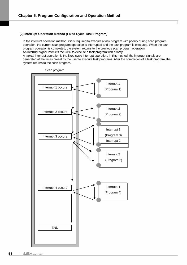
Chapter 5. Program Configuration and Operation Method
5-3
(2) Interrupt Operation Method (Fixed Cycle Task Program) In the interrupt operation method, if it is required to execute a task program with priority during scan program operation, the current scan program operation is interrupted and the task program is executed. When the task program operation is completed, the system returns to the previous scan program operation. An interrupt signal instructs the CPU to execute a task program with priority. A typical interrupt operation is the fixed cycle interrupt operation. In this method, the interrupt signals are generated at the times preset by the user to execute task programs. After the completion of a task program, the system returns to the scan program.
Scan program
Interrupt 1
(Program 1)
Interrupt 1 occurs
Interrupt 2
(Program 2)
Interrupt 2 occurs
Interrupt 3
(Program 3)
(프로그램 3)
Interrupt 3 occurs Interrupt 2
Interrupt 2
(Program 2)
Interrupt 4 occurs
Interrupt 4
(Program 4)
END
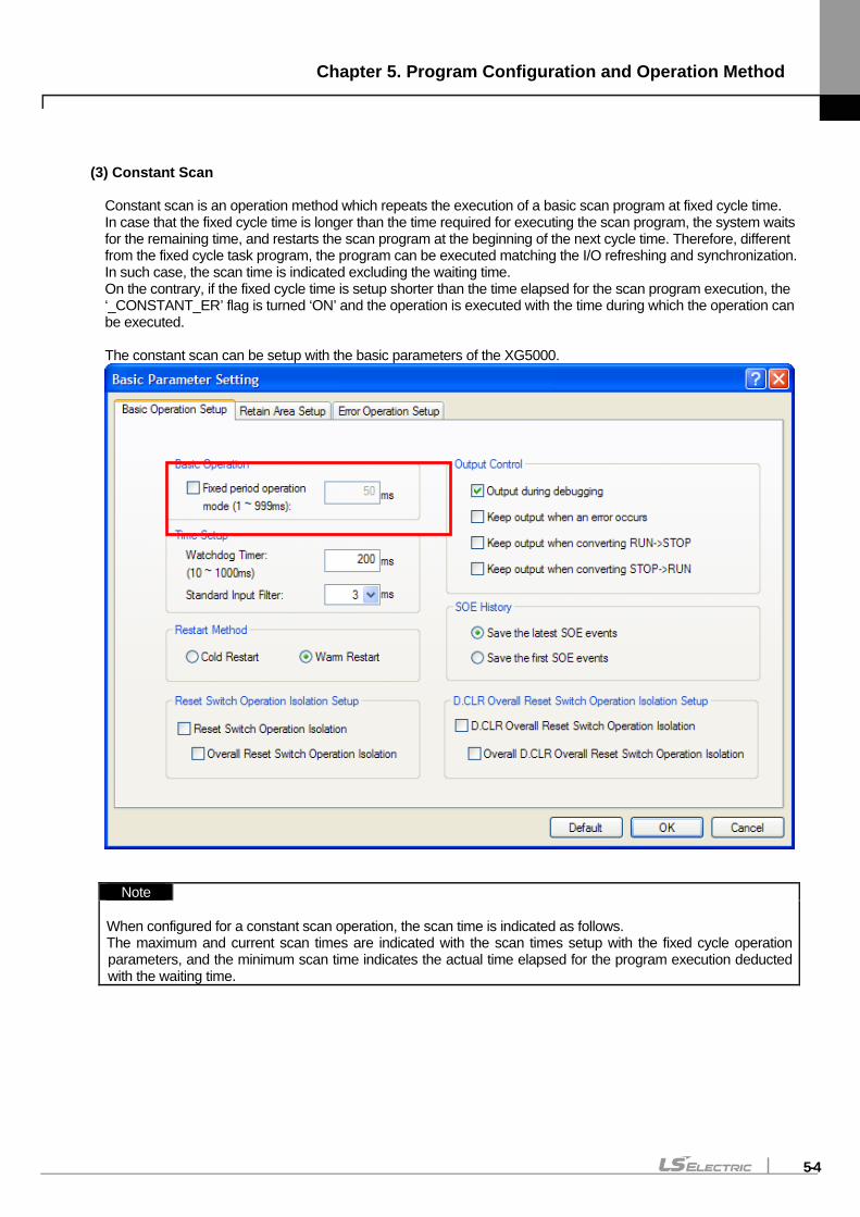
Chapter 5. Program Configuration and Operation Method
5-4
(3) Constant Scan Constant scan is an operation method which repeats the execution of a basic scan program at fixed cycle time. In case that the fixed cycle time is longer than the time required for executing the scan program, the system waits for the remaining time, and restarts the scan program at the beginning of the next cycle time. Therefore, different from the fixed cycle task program, the program can be executed matching the I/O refreshing and synchronization. In such case, the scan time is indicated excluding the waiting time. On the contrary, if the fixed cycle time is setup shorter than the time elapsed for the scan program execution, the ‘_CONSTANT_ER’ flag is turned ‘ON’ and the operation is executed with the time during which the operation can be executed. The constant scan can be setup with the basic parameters of the XG5000.
Note When configured for a constant scan operation, the scan time is indicated as follows. The maximum and current scan times are indicated with the scan times setup with the fixed cycle operation parameters, and the minimum scan time indicates the actual time elapsed for the program execution deducted with the waiting time.
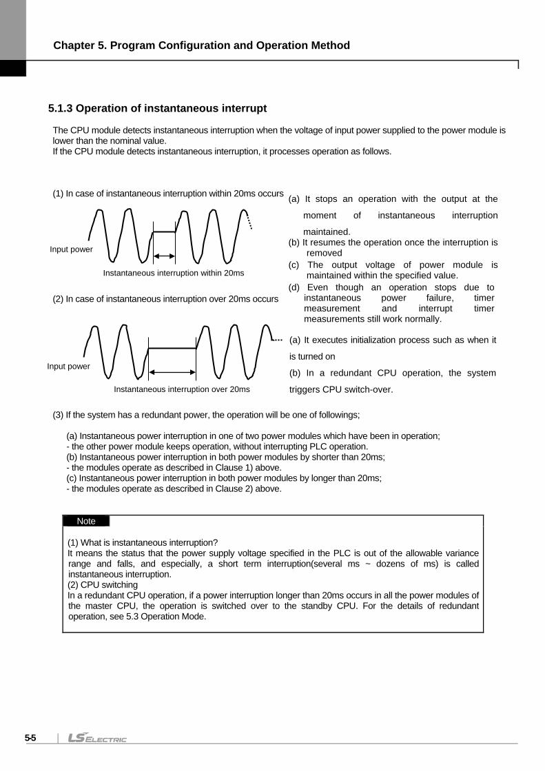
Chapter 5. Program Configuration and Operation Method
5-5
5.1.3 Operation of instantaneous interrupt The CPU module detects instantaneous interruption when the voltage of input power supplied to the power module is lower than the nominal value. If the CPU module detects instantaneous interruption, it processes operation as follows. (1) In case of instantaneous interruption within 20ms occurs (2) In case of instantaneous interruption over 20ms occurs (3) If the system has a redundant power, the operation will be one of followings;
(a) Instantaneous power interruption in one of two power modules which have been in operation; - the other power module keeps operation, without interrupting PLC operation. (b) Instantaneous power interruption in both power modules by shorter than 20ms; - the modules operate as described in Clause 1) above. (c) Instantaneous power interruption in both power modules by longer than 20ms; - the modules operate as described in Clause 2) above.
Note (1) What is instantaneous interruption? It means the status that the power supply voltage specified in the PLC is out of the allowable variance range and falls, and especially, a short term interruption(several ms ~ dozens of ms) is called instantaneous interruption. (2) CPU switching In a redundant CPU operation, if a power interruption longer than 20ms occurs in all the power modules of the master CPU, the operation is switched over to the standby CPU. For the details of redundant operation, see 5.3 Operation Mode.
Input power
Instantaneous interruption within 20ms
(a) It stops an operation with the output at the
moment of instantaneous interruption
maintained. (b) It resumes the operation once the interruption is
removed (c) The output voltage of power module is
maintained within the specified value. (d) Even though an operation stops due to
instantaneous power failure, timer measurement and interrupt timer measurements still work normally.
Input power
Instantaneous interruption over 20ms
(a) It executes initialization process such as when it
is turned on
(b) In a redundant CPU operation, the system
triggers CPU switch-over.
Chapter 5. Program Configuration and Operation Method
5-6
5.1.4 Scan Time The time required to complete all steps from the first step (0 step) to last step, that is, a time taken for one control operation is called ‘scan time.’ It is directly related to the control performance of the system. (1) Operation and performance of XGR
The major factors which influence scan time are program operation time, I/O data process time, communication service time, and the data synchronization between the master and standby CPUs. By utilizing the hardware relay method for the data exchange between expansion drive modules, the data communication performance of the XGR is greatly improved. In addition, the scan time is greatly reduced by MPU’s ladder program execution and the paralleled execution of the I/O data scanning by bus controller. In a single CPU operation, the scan process times of CPU are as follows.
Item Content to be processed time Process time of scan program Scan program+ Task program 42ns per 4 byte of execution
program
Process time of basic base Module process Communication module: within
200 per one Communication service Within 500 per one service
Process time of Expansion base
Every expansion base Within 300 per one base
Module process
Digital I/O: within 10 per one Special module: within 30 Communication module: within 150
Communication service Within 1000 per service
PUT/GET instruction process
Different according to data ~ 0.5 kbyte : 800 or less ~ 1 kbyte : 2.5 or less ~ 4 kbyte : 8 or less ~ 8 kbyte : 15 or less
Process time of system Basic O/S process routine, module error check, Fault mask, I/O skip etc.
Different according to setting environment In case of normal operation, within 4ms
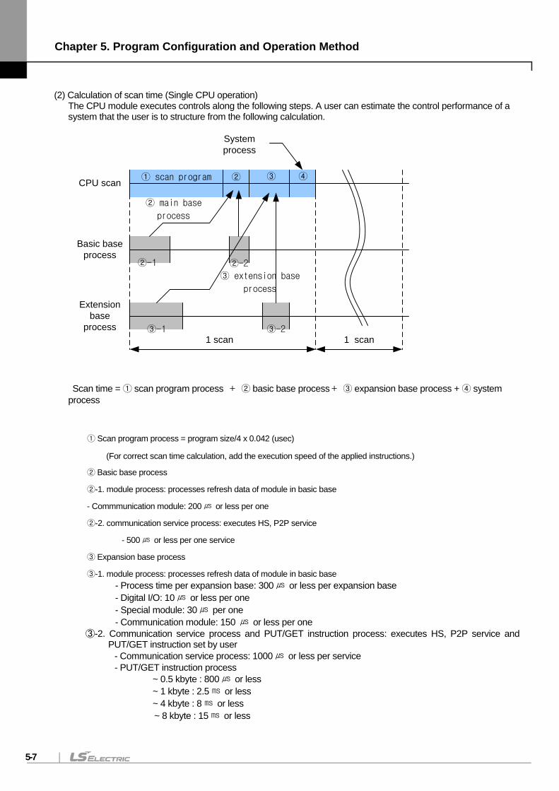
Chapter 5. Program Configuration and Operation Method
5-7
(2) Calculation of scan time (Single CPU operation)
The CPU module executes controls along the following steps. A user can estimate the control performance of a system that the user is to structure from the following calculation.
CPU scan
Basic base process
Extension base
process
① scan program
② main base
process
③ extension base
process
② ③ ④
System process
1 scan1 scan
②-2
③-2
②-1
③-1
Scan time = ① scan program process + ② basic base process+ ③ expansion base process + ④ system process
① Scan program process = program size/4 x 0.042 (usec)
(For correct scan time calculation, add the execution speed of the applied instructions.)
② Basic base process
②-1. module process: processes refresh data of module in basic base
- Commmunication module: 200 or less per one
②-2. communication service process: executes HS, P2P service
- 500 or less per one service
③ Expansion base process
③-1. module process: processes refresh data of module in basic base - Process time per expansion base: 300 or less per expansion base - Digital I/O: 10 or less per one - Special module: 30 per one - Communication module: 150 or less per one
③-2. Communication service process and PUT/GET instruction process: executes HS, P2P service and PUT/GET instruction set by user
- Communication service process: 1000 or less per service - PUT/GET instruction process
~ 0.5 kbyte : 800 or less ~ 1 kbyte : 2.5 or less ~ 4 kbyte : 8 or less ~ 8 kbyte : 15 or less
Chapter 5. Program Configuration and Operation Method
5-8
④ System process: executes system internal process includig basic O/S process routin, battery check, module error
check, I/O skip, forced I/O, loader service etc.
- different according to the environment In case of normal 4ms or less
Example
CPU(program 32KB) + 6 32-point I/O modules + 6 analog modules (total PUT/GET size 1000byte) + 4 communication modules (two in basic base, other two in expansion base, one communication service setting for each module) What is the scan time of above system (the number of expansion base is 2) Scan time() = ladder process time + basic base process time + expansion base process time + system process time = (32768/4 x 0.042) + (200 x 2(two communication modules) + 500 x 2) + (300 x 2(expansion base) + (10 x 6)+(30 x 6)+(150 x 2) + 1000 x 2 + 2500(PUT/GET)) + (4000) = 11384 = 11.4
(3) Scan time monitor
In an actual XGR CPU operation, the actual scan time can be obtained by monitoring following data. (1) Scan time is saved into the following flag(F) areas.
_SCAN_MAX : max. value of scan time(unit of 0.1ms)
_SCAN_MIN : min. value of scan time(unit of 0.1ms)
_SCAN_CUR : current value of scan time (unit of 0.1ms)
_SCAN_MAX, _SCAN_MIN value can be initialized using _SCAN_WR flag.
If the _SCAN_MAX is larger than WDT (Watch Dog Timer) value, a system error occurs. The WDT time can be setup
with the basic parameters.
(4) Scan Time in Redundant Operation
In redundant operations, compared with single CPU operation, the scan time substantially increases due to the system data sharing between the CPUs. The scan time also varies according to the data volume setup by the user in the redundancy parameter setting area. The increase in the scan time by data volume is as follows.
Chapter 5. Program Configuration and Operation Method
5-9
Redundancy parameter Contents Operation
Hot swapping option
Base Though base error occurs in normal RUN mode, system except that base operates. And if that base is restored, it operates normally.
Module Though module is disabled, module detachment error doesn’t appear. If that module is enabled, it operates normally.
Expansion base power failure setup
Restart and wait When two power modules of expansion base are off, system goes to WAIT mode (Ebxx)
Base power failure error When two power modules of expansion base are off, CPU error appears
Warning option
Disable warning for single power operation
Disables warning message when one between two power modules in expansion base is off
Disable warning for line Topology Disables warning message when becoming line topology
Disable warning for Single CPU Mode Disables warning message when becoming Single CPU Mode
Disable warning message for fault mask removal
Disables warning message when fault mask is removed.
Communication operation setting
Disconnection of the cable When the cable is disconnected, it is instantly switched. (within 1s)
Disconnection of the server connection
Master automatic switchover (redundancy operation) When Master/Standby is acting as FEnet server, if the cable of the Master is disconnected, Standby becomes Master.
(a) Redundant CPU system data: share basic data, e.g., system flag, communication flag, etc. (2.8ms) (b) Redundancy parameter setting data: synchronization time in each area is as follows;
I/Q base: 1ms/32 bases M area: approx. 250 per 2 kwords. Approx. 16 ms for synchronizing 128kword R area: approx. 1.5ms per 2 kword. Approx. 12ms for max. 16 kword synchronization. (When 2 kword in R area is transmitted, 2 kword in W area are also transmitted; total 4 kword are transmitted) PID Area: 016.7 required for each PID setting one loop. When max. 8 blocks are synchronized, approx. 4ms is required. Automatic variable area: 32KB 2.5ms required
Example
CPU(program 32KB) + 6 32-point I/O modules + 6 analog modules (total PUT/GET size 1000byte) + 4 communication modules(two in basic base, other two in expansion base, one communication service for each one module) what is the scan time of above system? (Two expansion bases, synchronizes M area 2kword and PID 2 blocks)
Redundancy Run scan time = single Run scan time + time for synchronizing redundancy data = Single Run scan time + redundancy system data+ I/O base + synchronizing M area and PID area = 11.4ms + 2.8ms + 1ms + 0.25ms + 0.5 x 2 = 16.45
Chapter 5. Program Configuration and Operation Method
5-10
(5) Delay Time at Entering Redundancy Operation
When a redundant CPU is added to single CPU operation, the scan time of the current scan cycle is increased temporarily, for the standby CPU to be initiated to enter redundancy operation mode. Since the data synchronization is carried out by 10% equivalent to the scan time of single operation, the scan time during the data synchronization increases by about 10% compared with single operation.
(1) When the standby CPU is activated to change the system from single operation to redundant operation, the scan time increases for a short time to synchronize the program and data from the master CPU to the standby CPU.
(2) It should be noted that, during single mode operation, including when the standby CPU is not in operation, data is not synchronized between the master CPU and standby CPU. Therefore, the data may differ from each other CPU.
Caution
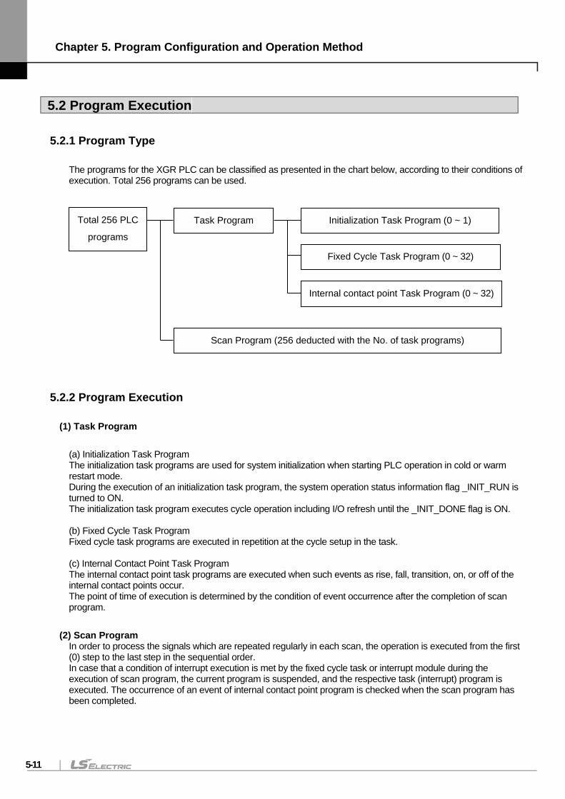
Chapter 5. Program Configuration and Operation Method
5-11
5.2 Program Execution
5.2.1 Program Type
The programs for the XGR PLC can be classified as presented in the chart below, according to their conditions of execution. Total 256 programs can be used.
5.2.2 Program Execution
(1) Task Program
(a) Initialization Task Program The initialization task programs are used for system initialization when starting PLC operation in cold or warm restart mode. During the execution of an initialization task program, the system operation status information flag _INIT_RUN is turned to ON. The initialization task program executes cycle operation including I/O refresh until the _INIT_DONE flag is ON. (b) Fixed Cycle Task Program Fixed cycle task programs are executed in repetition at the cycle setup in the task. (c) Internal Contact Point Task Program The internal contact point task programs are executed when such events as rise, fall, transition, on, or off of the internal contact points occur. The point of time of execution is determined by the condition of event occurrence after the completion of scan program.
(2) Scan Program In order to process the signals which are repeated regularly in each scan, the operation is executed from the first (0) step to the last step in the sequential order. In case that a condition of interrupt execution is met by the fixed cycle task or interrupt module during the execution of scan program, the current program is suspended, and the respective task (interrupt) program is executed. The occurrence of an event of internal contact point program is checked when the scan program has been completed.
Task Program Initialization Task Program (0 ~ 1)
Fixed Cycle Task Program (0 ~ 32)
Internal contact point Task Program (0 ~ 32)
Scan Program (256 deducted with the No. of task programs)
Total 256 PLC
programs
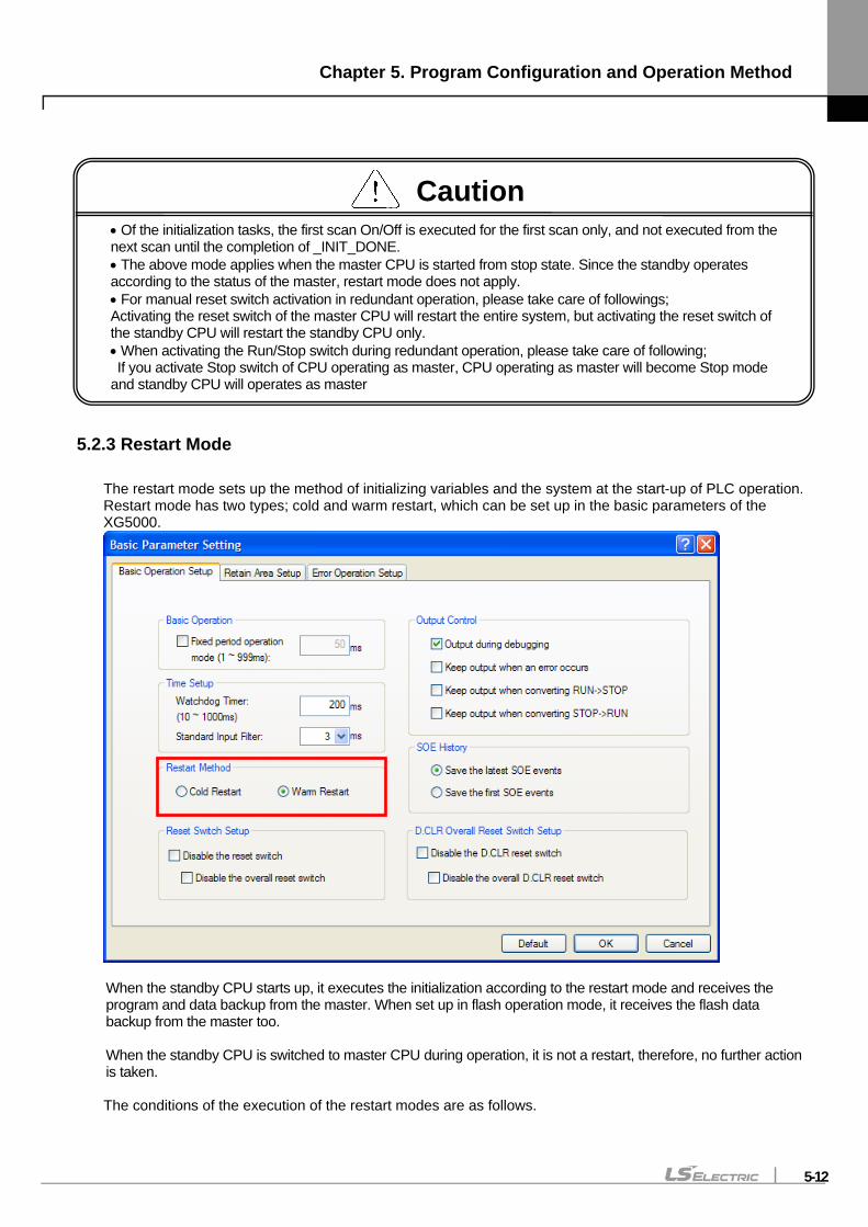
Chapter 5. Program Configuration and Operation Method
5-12
5.2.3 Restart Mode
The restart mode sets up the method of initializing variables and the system at the start-up of PLC operation. Restart mode has two types; cold and warm restart, which can be set up in the basic parameters of the XG5000.
When the standby CPU starts up, it executes the initialization according to the restart mode and receives the program and data backup from the master. When set up in flash operation mode, it receives the flash data backup from the master too. When the standby CPU is switched to master CPU during operation, it is not a restart, therefore, no further action is taken. The conditions of the execution of the restart modes are as follows.
• Of the initialization tasks, the first scan On/Off is executed for the first scan only, and not executed from the next scan until the completion of _INIT_DONE. • The above mode applies when the master CPU is started from stop state. Since the standby operates according to the status of the master, restart mode does not apply. • For manual reset switch activation in redundant operation, please take care of followings; Activating the reset switch of the master CPU will restart the entire system, but activating the reset switch of the standby CPU will restart the standby CPU only. • When activating the Run/Stop switch during redundant operation, please take care of following; If you activate Stop switch of CPU operating as master, CPU operating as master will become Stop mode and standby CPU will operates as master
Caution
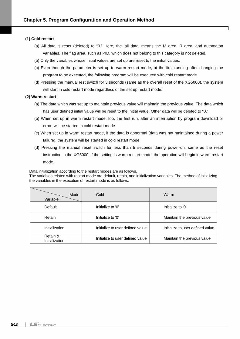
Chapter 5. Program Configuration and Operation Method
5-13
(1) Cold restart (a) All data is reset (deleted) to “0.” Here, the ‘all data’ means the M area, R area, and automaton
variables. The flag area, such as PID, which does not belong to this category is not deleted.
(b) Only the variables whose initial values are set up are reset to the initial values.
(c) Even though the parameter is set up to warm restart mode, at the first running after changing the
program to be executed, the following program will be executed with cold restart mode.
(d) Pressing the manual rest switch for 3 seconds (same as the overall reset of the XG5000), the system
will start in cold restart mode regardless of the set up restart mode.
(2) Warm restart (a) The data which was set up to maintain previous value will maintain the previous value. The data which
has user defined initial value will be reset to the initial value. Other data will be deleted to “0.”
(b) When set up in warm restart mode, too, the first run, after an interruption by program download or
error, will be started in cold restart mode.
(c) When set up in warm restart mode, if the data is abnormal (data was not maintained during a power
failure), the system will be started in cold restart mode.
(d) Pressing the manual reset switch for less than 5 seconds during power-on, same as the reset
instruction in the XG5000, if the setting is warm restart mode, the operation will begin in warm restart
mode. Data initialization according to the restart modes are as follows. The variables related with restart mode are default, retain, and initialization variables. The method of initializing the variables in the execution of restart mode is as follows.
Mode
Variable Cold Warm
Default Initialize to ‘0’ Initialize to ‘0’
Retain Initialize to ‘0’ Maintain the previous value
Initialization Initialize to user defined value Initialize to user defined value
Retain & Initialization Initialize to user defined value Maintain the previous value
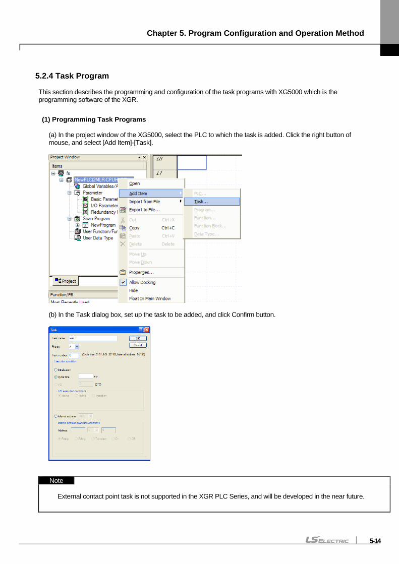
Chapter 5. Program Configuration and Operation Method
5-14
5.2.4 Task Program This section describes the programming and configuration of the task programs with XG5000 which is the programming software of the XGR.
(1) Programming Task Programs (a) In the project window of the XG5000, select the PLC to which the task is added. Click the right button of mouse, and select [Add Item]-[Task].
(b) In the Task dialog box, set up the task to be added, and click Confirm button.
Note
External contact point task is not supported in the XGR PLC Series, and will be developed in the near future.
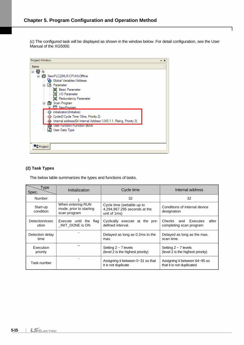
Chapter 5. Program Configuration and Operation Method
5-15
(c) The configured task will be displayed as shown in the window below. For detail configuration, see the User Manual of the XG5000.
(2) Task Types The below table summarizes the types and functions of tasks.
Type Spec. Initialization Cycle time Internal address
Number 1 32 32
Start-up condition
When entering RUN mode, prior to starting scan program
Cycle time (settable up to 4,294,967.295 seconds at the unit of 1ms)
Conditions of internal device designation
Detection/execution
Execute until the flag _INIT_DONE is ON
Cyclically execute at the pre-defined interval.
Checks and Executes after completing scan program
Detection delay time
- Delayed as long as 0.2ms to the max.
Delayed as long as the max. scan time.
Execution priority
-- Setting 2 ~ 7 levels (level 2 is the highest priority)
Setting 2 ~ 7 levels (level 2 is the highest priority)
Task number - Assigning it between 0~31 so that
it is not duplicate Assigning it between 64~95 so that it is not duplicated
Chapter 5. Program Configuration and Operation Method
5-16
(3) Processing method of task program It describes the common processing method and cautions of task program (a) Features of task program
Task program does not reiteratively be processed like a scan program and instead, it is executed only when the
execution conditions occur. Make sure to remember this when creating a task program.
For instance, if a task program with 10 seconds of fixed cycle is used with a timer and counter, the timer may have an
error of 10 seconds maximum while the counter checks every 10 seconds, any counter input changed within 10 seconds
is not counted.
(b) Execution priority
If several tasks to execute are waiting, it processes from the highest priority task program. If there are several tasks of
same priority, they are processed by the order which is occurred.
The task priority is applied to only each task.
Please set the priority of task program considering program features, importance level and urgency demanding
execution.
(c) Process delay time
The delay of task program processing occurs due to the following factors. Make sure to consider them when setting a
task or creating a program.
Task detection delay(please refer to the details of each task)
Program execution delay due to the execution of preceding task program
(d) Correlation between scan program and task program in the initialization
Fixed Cycle task and internal contact point task does not operate while initialization task program is working.
Since scan program has a low priority, if a task occurs, it stops a scan program and executes a task program. Therefore,
if tasks frequently occur during one scan, a scan time may increase unreasonably. A special attention should be paid
when setting the conditions of task.
Chapter 5. Program Configuration and Operation Method
5-17
(e) Protection from task program of a currently running program
If program execution continuity is lost by executing a higher priority program, you can partially protect the task program
from being executed, for a problematic part. At the moment, a program can be protected by application function
commands of ‘DI (task program operation disabled)’ or ‘EI(task program operation enabled)’
Insert the application function command, ‘DI’ into the beginning position of a section to be protected and the
application function command, ‘EI’ to the position to cancel it. Initialization task is not affected by the application
function commands of ‘DI’ and ‘EI’.
Note
(1) If task program priority is duplicate set, a program works according to the creation order.
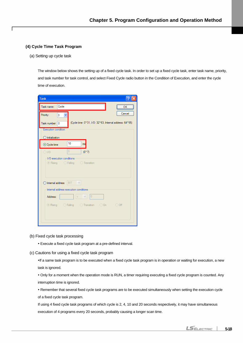
Chapter 5. Program Configuration and Operation Method
5-18
(4) Cycle Time Task Program (a) Setting up cycle task
The window below shows the setting up of a fixed cycle task. In order to set up a fixed cycle task, enter task name, priority,
and task number for task control, and select Fixed Cycle radio button in the Condition of Execution, and enter the cycle
time of execution.
(b) Fixed cycle task processing
Execute a fixed cycle task program at a pre-defined interval. (c) Cautions for using a fixed cycle task program
If a same task program is to be executed when a fixed cycle task program is in operation or waiting for execution, a new
task is ignored.
Only for a moment when the operation mode is RUN, a timer requiring executing a fixed cycle program is counted. Any
interruption time is ignored.
Remember that several fixed cycle task programs are to be executed simultaneously when setting the execution cycle
of a fixed cycle task program.
If using 4 fixed cycle task programs of which cycle is 2, 4, 10 and 20 seconds respectively, it may have simultaneous
execution of 4 programs every 20 seconds, probably causing a longer scan time.
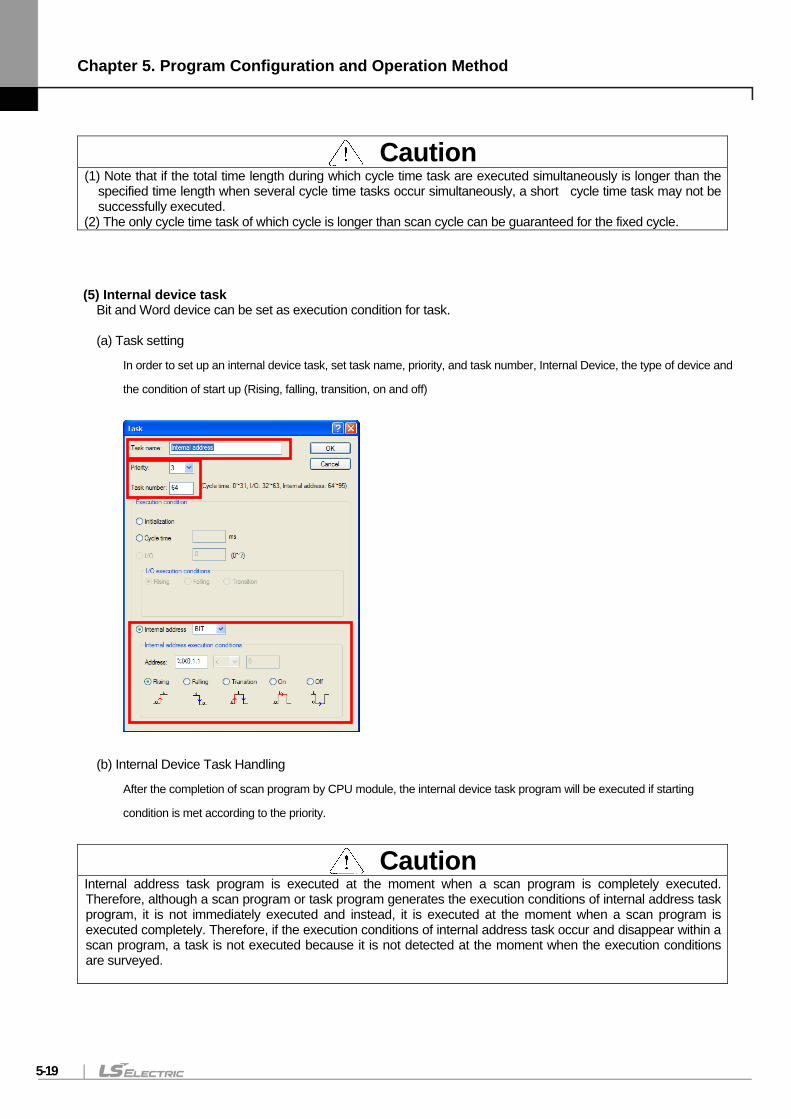
Chapter 5. Program Configuration and Operation Method
5-19
(5) Internal device task Bit and Word device can be set as execution condition for task. (a) Task setting
In order to set up an internal device task, set task name, priority, and task number, Internal Device, the type of device and
the condition of start up (Rising, falling, transition, on and off)
(b) Internal Device Task Handling
After the completion of scan program by CPU module, the internal device task program will be executed if starting
condition is met according to the priority.
Caution (1) Note that if the total time length during which cycle time task are executed simultaneously is longer than the
specified time length when several cycle time tasks occur simultaneously, a short cycle time task may not be successfully executed.
(2) The only cycle time task of which cycle is longer than scan cycle can be guaranteed for the fixed cycle.
Caution Internal address task program is executed at the moment when a scan program is completely executed. Therefore, although a scan program or task program generates the execution conditions of internal address task program, it is not immediately executed and instead, it is executed at the moment when a scan program is executed completely. Therefore, if the execution conditions of internal address task occur and disappear within a scan program, a task is not executed because it is not detected at the moment when the execution conditions are surveyed.
Chapter 5. Program Configuration and Operation Method
5-20
(6) Task processing in instantaneous interruption When resuming operation due to a long instantaneous interruption, ignore any waiting task and tasks that occur during the interruption and process the only tasks from the moment of starting operation. If an interruption is within 20ms, a task that was waiting is executed once the interruption is removed. Any fixed cycle interrupt task that is duplicated during the interruption is ignored.
(7) Verification of task program After creating a task program, verify it in accordance with the followings. (a) Is the task set properly?
If a task occurs excessively or several tasks occur simultaneously in a scan, it may cause longer scan time or irregularity
If a task setting can not be changed, check the max. scan time.
(b) Is the task priority well arranged?
A low priority task program may not be processed in a specified time due to a delay from a higher priority task program.
The case may be, since the next task occurs with a preceding task delayed, it may cause task collision. The priority
should be set in consideration of urgency of task, execution time and etc.
(c) Is the task program created as short as possible?
A longer execution time of task program may cause a longer scan time or irregularity. In addition, it may cause task
program collision. Make sure to set the execution time as short as possible(especially, create a fixed cycle task program
so that it could be executed within 10% of the shortest task cycle among several tasks. )
(d) Doesn’t the program need to be protected against the highest priority task during the execution of program?
If a different task breaks into a task program execution, it completes a current task and then, operates from a task with the
highest priority among waiting tasks. In case it is prohibited that a different task breaks into a scan program, it can be
protected by using ‘DI’/’EI’ application functional commands. It may cause a trouble while processing a global
parameter process commonly used with other program or a special or communication module.
(8) Program configuration and example of processing First of all, register task and program as follows.
• Registering a task :
T_SLOW (fixed cycle : = 10ms, Priority := 3 )
PROC_1 (internal contact : = M0, Priority := 5 )
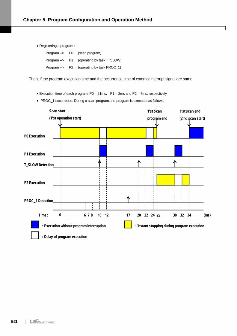
Chapter 5. Program Configuration and Operation Method
5-21
• Registering a program :
Program --> P0 (scan program)
Program --> P1 (operating by task T_SLOW)
Program --> P2 (operating by task PROC_1)
Then, if the program execution time and the occurrence time of external interrupt signal are same,
• Execution time of each program: P0 = 21ms, P1 = 2ms and P2 = 7ms, respectively
• PROC_1 occurrence: During a scan program, the program is executed as follows.
P0 Execution
P1 Execution
P2 Execution
T_SLOW Detection
PROC_1 Detection
Time : 0 6 7 8 10 12 17 20 22 24 25 30 32 34 (ms)
Scan start
(1’st operation start) 1’st Scan
program end
1’st scan end
(2’nd scan start)
: Execution without program interruption
: Delay of program execution
: Instant stopping during program execution
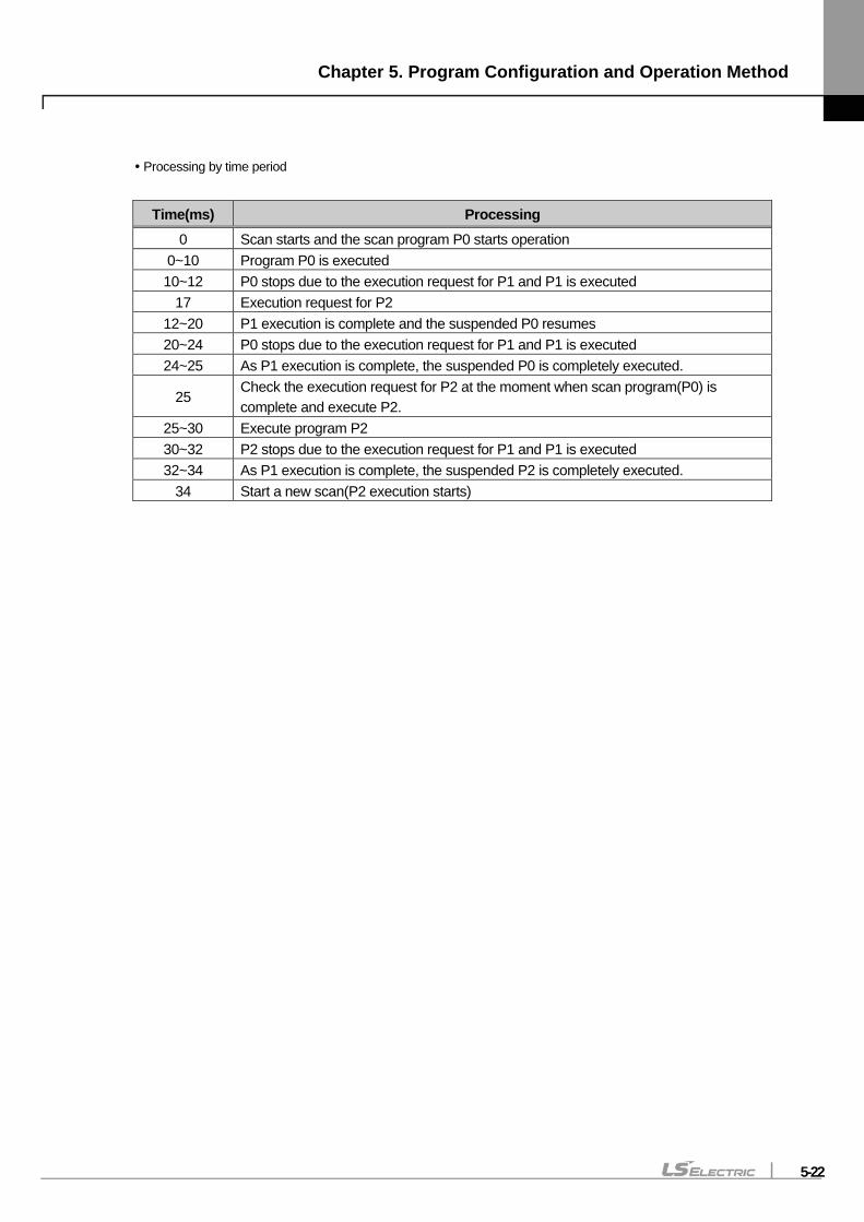
Chapter 5. Program Configuration and Operation Method
5-22
Processing by time period
Time(ms) Processing
0 Scan starts and the scan program P0 starts operation 0~10 Program P0 is executed 10~12 P0 stops due to the execution request for P1 and P1 is executed
17 Execution request for P2 12~20 P1 execution is complete and the suspended P0 resumes 20~24 P0 stops due to the execution request for P1 and P1 is executed 24~25 As P1 execution is complete, the suspended P0 is completely executed.
25 Check the execution request for P2 at the moment when scan program(P0) is complete and execute P2.
25~30 Execute program P2 30~32 P2 stops due to the execution request for P1 and P1 is executed 32~34 As P1 execution is complete, the suspended P2 is completely executed.
34 Start a new scan(P2 execution starts)
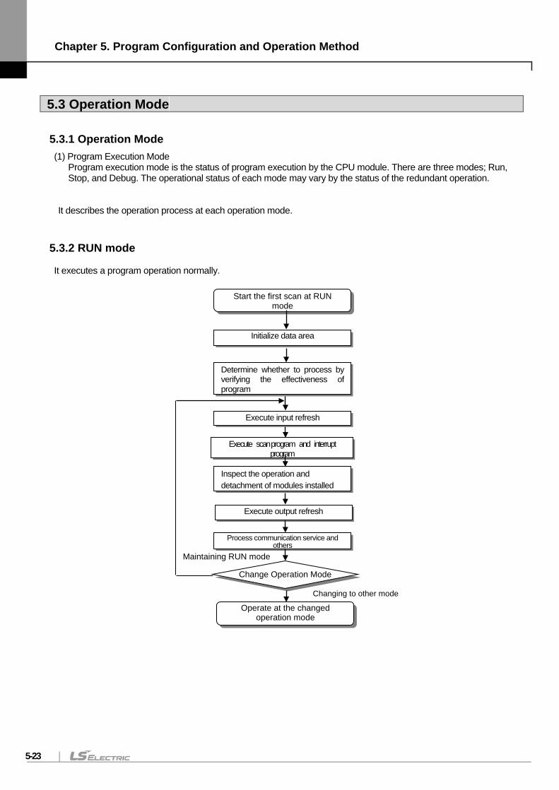
Chapter 5. Program Configuration and Operation Method
5-23
5.3 Operation Mode
5.3.1 Operation Mode
(1) Program Execution Mode Program execution mode is the status of program execution by the CPU module. There are three modes; Run, Stop, and Debug. The operational status of each mode may vary by the status of the redundant operation.
It describes the operation process at each operation mode.
5.3.2 RUN mode It executes a program operation normally.
Start the first scan at RUN mode
Initialize data area
Determine whether to process by verifying the effectiveness of program
Execute input refresh
Execute scan program and interrupt program
Inspect the operation and detachment of modules installed
Process communication service and others
Execute output refresh
Change Operation Mode
Maintaining RUN mode
Changing to other mode
Operate at the changed operation mode
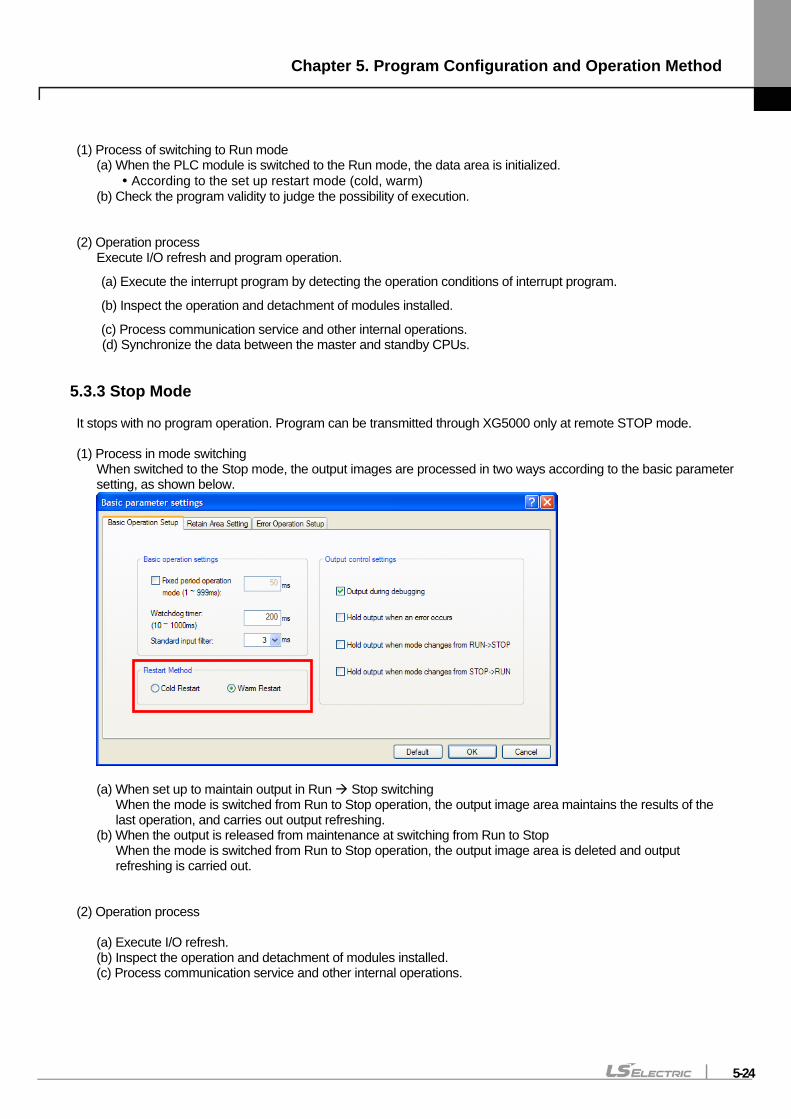
Chapter 5. Program Configuration and Operation Method
5-24
(1) Process of switching to Run mode
(a) When the PLC module is switched to the Run mode, the data area is initialized. According to the set up restart mode (cold, warm)
(b) Check the program validity to judge the possibility of execution.
(2) Operation process Execute I/O refresh and program operation.
(a) Execute the interrupt program by detecting the operation conditions of interrupt program.
(b) Inspect the operation and detachment of modules installed.
(c) Process communication service and other internal operations. (d) Synchronize the data between the master and standby CPUs.
5.3.3 Stop Mode It stops with no program operation. Program can be transmitted through XG5000 only at remote STOP mode. (1) Process in mode switching
When switched to the Stop mode, the output images are processed in two ways according to the basic parameter setting, as shown below.
(a) When set up to maintain output in Run Stop switching
When the mode is switched from Run to Stop operation, the output image area maintains the results of the last operation, and carries out output refreshing.
(b) When the output is released from maintenance at switching from Run to Stop When the mode is switched from Run to Stop operation, the output image area is deleted and output refreshing is carried out.
(2) Operation process
(a) Execute I/O refresh. (b) Inspect the operation and detachment of modules installed. (c) Process communication service and other internal operations.
Chapter 5. Program Configuration and Operation Method
5-25
5.3.4 Debug Mode As a mode to find any error from a program or trace an operation procedure, the mode can be changed only from STOP mode. In the mode, a user can verify a program while checking the program execution and data. (1) Processing when a mode is changed
(a) At the beginning when the mode is changed, initialize the data area. (b) Clear the output image area and execute input refresh.
(2) Operation process
(a) Execute I/O refresh. (b) Debugging operation depending on the settings. (c) After completing debugging operation to the end of the program, it executes output refresh. (d) Inspect the operation and detachment of modules installed. (e) Process communication service and other internal operations.
(3) Conditions of debug operation
There are four types of debug operation conditions and if reaching the break point, it is possible to set a different type of break point.
Operation condition Description
Stepwise execution of operation(step over) Upon an operation command, it executes a unit of operation and stops
Execution according to the designation of break point
Once a break point is designated in a program, it stops at the designated point
Execution according to the status of contact
If designating the contact area to monitor and the status(read, write, value), it stops when the designated operation occurs at the pre-defined contact.
Execution according to the designated scan frequency
Once designating the scan frequency to operation, it stops after operating as many as the scan frequency designated.
(4) Operation method
(a) Set the debug operation conditions at XG5000 and execute the operation. (b) The interrupt program can be set by enabled/disabled at the unit of each interrupt.
(For the details of operation, please refer to Chapter 12 Debugging in the user’s manual of XG5000)
5.3.5 Switching Operation Mode (1) How to change an operation mode
An operation mode can be changed as follows.
Caution 1. Debug mode is only available in single system.
(1) To use debug mode, turn off the power of standby CPU and so that the system runs in single. (2) Convert to remote stop mode by mode key switch.
2. During debug mode, the user can’t change mode by mode switch.
Chapter 5. Program Configuration and Operation Method
5-26
(a) Mode change by the mode key of the CPU module (b) Change by accessing the programming tool(XG5000) to a communication port of CPU (c) Change of a different CPU module networked by XG5000 accessed to a communication port of CPU (d) Change by using XG5000, HMI and computer link module, which are networked. (e) Change by ‘STOP’ command while a program is operating.
(2) Type of Operation Mode
(a) Changing program execution mode with mode key
the method of changing operation mode using mode key is as follows.
Mode Key Position Operation Mode
RUN Local RUN
STOP Local STOP
STOP → REM Remote STOP REM → RUN Local RUN RUN → REM Remote RUN
REM → STOP Local STOP (b) Changing remote operation mode
Changing remote modes can be done with the operation mode switch at ‘Remote Allowed: REM.’
Mode Key Position Mode change Mode change by XG5000 Change by computer
communication, etc.
REM
Remote STOP → Remote RUN O O(review)
Remote STOP → DEBUG O X Remote RUN → Remote STOP O O
Remote RUN → DEBUG X X
DEBUG → Remote STOP O O DEBUG → Remote RUN X X
Caution If changing the remote ‘RUN’ mode to ‘RUN’ mode by switch, the PLC is continuously operating without suspension. Editing during RUN is possible in the ‘RUN’ mode by switch, but the mode change by XG5000 is restricted. Make sure to change it only when the mode change is not remotely allowed.
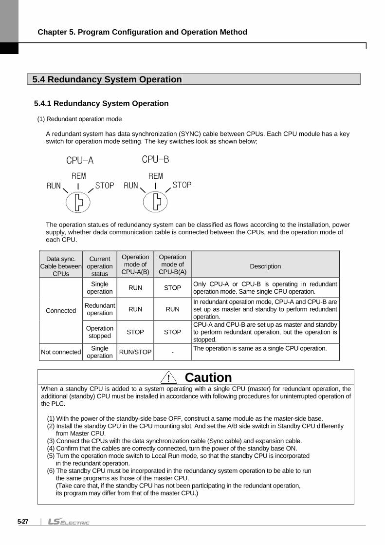
Chapter 5. Program Configuration and Operation Method
5-27
5.4 Redundancy System Operation
5.4.1 Redundancy System Operation (1) Redundant operation mode
A redundant system has data synchronization (SYNC) cable between CPUs. Each CPU module has a key switch for operation mode setting. The key switches look as shown below;
The operation statues of redundancy system can be classified as flows according to the installation, power supply, whether dada communication cable is connected between the CPUs, and the operation mode of each CPU.
Data sync. Cable between
CPUs
Current operation
status
Operation mode of
CPU-A(B)
Operation mode of
CPU-B(A) Description
Connected
Single operation RUN STOP Only CPU-A or CPU-B is operating in redundant
operation mode. Same single CPU operation.
Redundant operation RUN RUN
In redundant operation mode, CPU-A and CPU-B are set up as master and standby to perform redundant operation.
Operation stopped STOP STOP
CPU-A and CPU-B are set up as master and standby to perform redundant operation, but the operation is stopped.
Not connected Single operation RUN/STOP - The operation is same as a single CPU operation.
Caution When a standby CPU is added to a system operating with a single CPU (master) for redundant operation, the additional (standby) CPU must be installed in accordance with following procedures for uninterrupted operation of the PLC. (1) With the power of the standby-side base OFF, construct a same module as the master-side base. (2) Install the standby CPU in the CPU mounting slot. And set the A/B side switch in Standby CPU differently from Master CPU. (3) Connect the CPUs with the data synchronization cable (Sync cable) and expansion cable. (4) Confirm that the cables are correctly connected, turn the power of the standby base ON. (5) Turn the operation mode switch to Local Run mode, so that the standby CPU is incorporated in the redundant operation. (6) The standby CPU must be incorporated in the redundancy system operation to be able to run the same programs as those of the master CPU. (Take care that, if the standby CPU has not been participating in the redundant operation, its program may differ from that of the master CPU.)
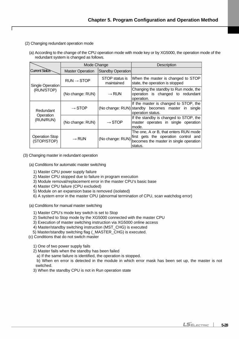
Chapter 5. Program Configuration and Operation Method
5-28
(2) Changing redundant operation mode
(a) According to the change of the CPU operation mode with mode key or by XG5000, the operation mode of the
redundant system is changed as follows.
Current Status
Mode Change Description Master Operation Standby Operation
Single Operation (RUN/STOP)
RUN → STOP STOP status is maintained
When the master is changed to STOP state, the operation is stopped
(No change: RUN) → RUN Changing the standby to Run mode, the operation is changed to redundant operation.
Redundant Operation
(RUN/RUN)
→ STOP (No change: RUN) If the master is changed to STOP, the standby becomes master in single operation status.
(No change: RUN) → STOP If the standby is changed to STOP, the master operates in single operation mode.
Operation Stop (STOP/STOP) → RUN (No change: RUN)
The one, A or B, that enters RUN mode first gets the operation control and becomes the master in single operation status.
(3) Changing master in redundant operation
(a) Conditions for automatic master switching
1) Master CPU power supply failure 2) Master CPU stopped due to failure in program execution 3) Module removal/replacement error in the master CPU‘s basic base 4) Master CPU failure (CPU excluded) 5) Module on an expansion base is removed (isolated) 6) A system error in the master CPU (abnormal termination of CPU, scan watchdog error)
(a) Conditions for manual master switching
1) Master CPU’s mode key switch is set to Stop 2) Switched to Stop mode by the XG5000 connected with the master CPU 3) Execution of master switching instruction via XG5000 online access 4) Master/standby switching instruction (MST_CHG) is executed 5) Master/standby switching flag (_MASTER_CHG) is executed.
(c) Conditions that do not switch master
1) One of two power supply fails 2) Master fails when the standby has been failed
a) If the same failure is identified, the operation is stopped. b) When en error is detected in the module in which error mask has been set up, the master is not
switched. 3) When the standby CPU is not in Run operation state
Chapter 5. Program Configuration and Operation Method
5-29
5.4.2 Start-up of Redundant System (1) Programming
(a) Conduct programming with XG5000. (For details, see ‘XG5000 User Manual’.)
(b) Transmit the program
Transmit the program with XG5000.
(2) Starting methods
Following methods are available for starting-up PLC;
(a) Starting with local key: Download the program in remote mode (REM), set the front key to ‘RUN’
(b) Starting with XG5000: Set the front key on the CPU module to ‘REM,’ select RUN on the XG5000’s online menu.
(c) Starting by power ON: When the power is turned ON with the front key set to RUN or if the system was in Remote RUN mode before power OFF, the system can be started by power ON.
(d) Restarting with reset key: Restarting with reset key has two methods; Reset and Overall Reset
1) Reset: activated by pressing the reset button on the front of the CPU module less than 3 seconds.
‘RST’ will appear on the indicator panel of the CPU. This is the same as power ON/OFF.
2) Overall Reset: activated by pressing the reset button on the CPU module for more than 3 seconds. ‘RSTC’ will appear on the indicator panel of the CPU. When the button is released, the system will be restarted in cold restart.
(3) Beginning the first operation
The procedures of system setting-up and starting-up for the first time operation of a redundant system are as follows.
(a) Prepare the program bocks suitable for the purpose, in as independent forms as possible (b) In the redundancy parameters, set up the data synchronization area. (c) When the programming is completed, compile it and carry out debugging. (d) Using the XG5000 program tool, access CPU communication port and download the program (e) Switch CPU-A or B to RUN mode using the mode switch key or XG5000. (f) Switch the CPU which is not the master to RUN mode to set it to the standby CPU (g) Stop the CPU-A to check normal operation of the standby CPU-B.
(4) Participating in operation When the standby CPU participates in the operation while the master CPU is in operation, the standby CPU is synchronized with the master CPU in following procedures.
(a) CPU initialization (b) Checking the redundant components (c) Transfer non-variable data to the master (d) Transfer variable data from the master (e) Check synchronization with the master CPU (f) Participate in the operation at the same time as the master CPU
Chapter 5. Program Configuration and Operation Method
5-30
Note
(1) For the redundant operation mode setting and parameter setting, see ‘6.7 Redundant System Operation Mode’ (2) (a), (b), and (c) are processed separately with delay time less than approximately 50ms at every scan of the master. (3) (d), (e), and (f) must be processed within one scan of the master, with the delay time not exceeding 50ms. (If the volume of the variables used exceeds the standard variable value, the delay time may exceed 50ms. For further
information, see ‘5.1.4 Scan Time’)
(5) Procedures of participating in standby operation Detail procedures of participating in standby operation are as follows.
(a) Power ON
1) Check that the master is in operation 2) Standby entering mode 3) CPU self diagnosis 4) Transfer program from the master (store in RAM and memory module)
(b) Checking redundant system components
1) Check switching I/O access 2) Receive and check switching I/O module information from the master 3) Scan the redundant I/O module information installed in the standby-side 4) Compare with the I/O parameters
(c)Transfer non-variable data from the master
1) Receive the flag from the master (executed by being divided into multiple scans as necessary) 2) After confirming that the flag status has not been changed, proceed to (4)
(d) Receive the variable data from the maser 1) User data area and a part of system buffer
(e) Check synchronicity with the master 1) All the operation data in the CPU is synchronized
(f) Participate in the operation at the same time as the master 1) Conduct redundant operation from the input refreshing
(6) Operation according to starting status
(a) Normal start-up The master CPU module checks system configuration at power ON. In case of late power on of the expansion base, the base being check appears on the front indicator panel and wait for power on. In ‘STOP’ mode, wait for 10 seconds and switched to Stop mode. 1) The first operation after program modification begins in cold restart. 2) When the system had been shut-down normally, the restarting will be performed according to the set-up parameters, including mode key, XG5000, power OFF and reset. 3) To cold-restart a system set up in warm restart mode, use reset key or the Overall Reset function of the
XG5000. 4) If the system was stopped due to an error in operation, the restarting method will be determined by the
type and release method of the error (see ‘Chapter 13. Program Troubleshooting’).
(b) When I/O skip has been set up 1) Since the I/O module set up with skip is excluded from the operation in the restarting, failure check, etc.,
are not conducted, and included in the operation normally when the skip is released during operation. For detail information, see ‘9.2 I/O Skip’ and ‘9.3 Module Replacement during Operation.’
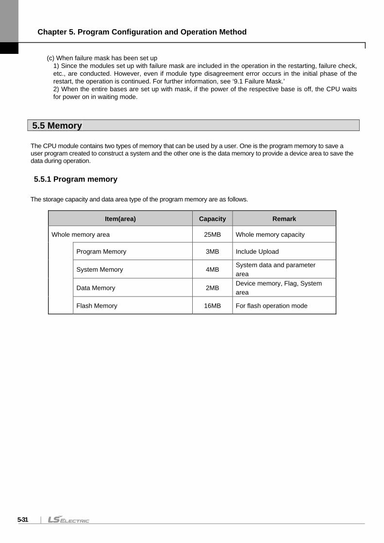
Chapter 5. Program Configuration and Operation Method
5-31
(c) When failure mask has been set up 1) Since the modules set up with failure mask are included in the operation in the restarting, failure check, etc., are conducted. However, even if module type disagreement error occurs in the initial phase of the restart, the operation is continued. For further information, see ‘9.1 Failure Mask.’ 2) When the entire bases are set up with mask, if the power of the respective base is off, the CPU waits for power on in waiting mode.
5.5 Memory The CPU module contains two types of memory that can be used by a user. One is the program memory to save a user program created to construct a system and the other one is the data memory to provide a device area to save the data during operation.
5.5.1 Program memory The storage capacity and data area type of the program memory are as follows.
Item(area) Capacity Remark
Whole memory area 25MB Whole memory capacity
Program Memory 3MB Include Upload
System Memory 4MB System data and parameter area
Data Memory 2MB Device memory, Flag, System area
Flash Memory 16MB For flash operation mode
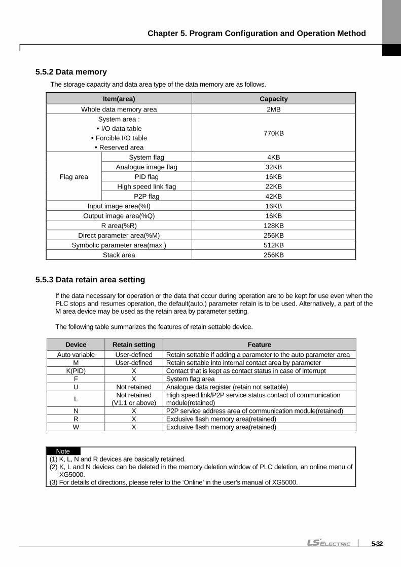
Chapter 5. Program Configuration and Operation Method
5-32
5.5.2 Data memory The storage capacity and data area type of the data memory are as follows.
Item(area) Capacity Whole data memory area 2MB
System area : I/O data table Forcible I/O table Reserved area
770KB
Flag area
System flag 4KB Analogue image flag 32KB
PID flag 16KB High speed link flag 22KB
P2P flag 42KB Input image area(%I) 16KB
Output image area(%Q) 16KB R area(%R) 128KB
Direct parameter area(%M) 256KB Symbolic parameter area(max.) 512KB
Stack area 256KB
5.5.3 Data retain area setting
If the data necessary for operation or the data that occur during operation are to be kept for use even when the PLC stops and resumes operation, the default(auto.) parameter retain is to be used. Alternatively, a part of the M area device may be used as the retain area by parameter setting.
The following table summarizes the features of retain settable device.
Device Retain setting Feature
Auto variable User-defined Retain settable if adding a parameter to the auto parameter area M User-defined Retain settable into internal contact area by parameter
K(PID) X Contact that is kept as contact status in case of interrupt F X System flag area U Not retained Analogue data register (retain not settable)
L Not retained (V1.1 or above)
High speed link/P2P service status contact of communication module(retained)
N X P2P service address area of communication module(retained) R X Exclusive flash memory area(retained) W X Exclusive flash memory area(retained)
Note (1) K, L, N and R devices are basically retained. (2) K, L and N devices can be deleted in the memory deletion window of PLC deletion, an online menu of
XG5000. (3) For details of directions, please refer to the ‘Online’ in the user’s manual of XG5000.
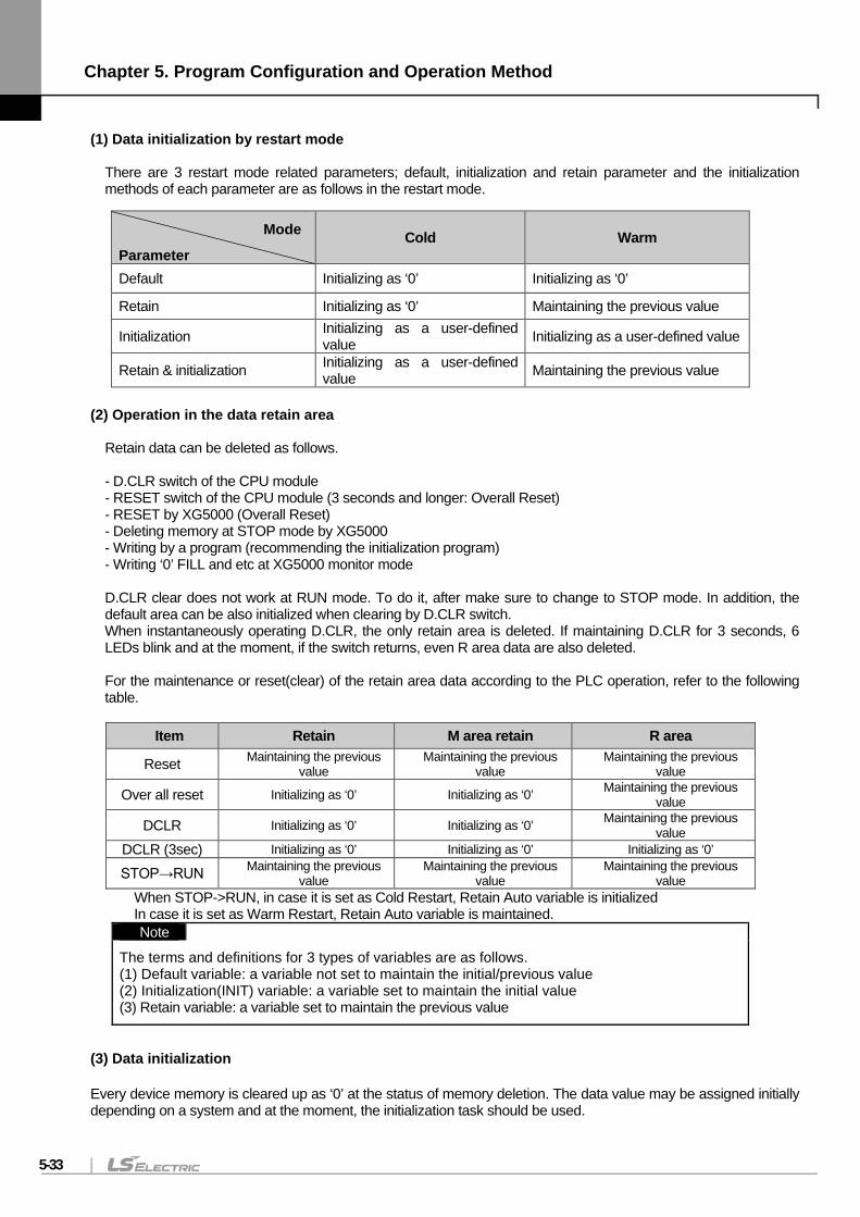
Chapter 5. Program Configuration and Operation Method
5-33
(1) Data initialization by restart mode
There are 3 restart mode related parameters; default, initialization and retain parameter and the initialization methods of each parameter are as follows in the restart mode.
(2) Operation in the data retain area Retain data can be deleted as follows. - D.CLR switch of the CPU module - RESET switch of the CPU module (3 seconds and longer: Overall Reset) - RESET by XG5000 (Overall Reset) - Deleting memory at STOP mode by XG5000 - Writing by a program (recommending the initialization program) - Writing ‘0’ FILL and etc at XG5000 monitor mode D.CLR clear does not work at RUN mode. To do it, after make sure to change to STOP mode. In addition, the default area can be also initialized when clearing by D.CLR switch. When instantaneously operating D.CLR, the only retain area is deleted. If maintaining D.CLR for 3 seconds, 6 LEDs blink and at the moment, if the switch returns, even R area data are also deleted. For the maintenance or reset(clear) of the retain area data according to the PLC operation, refer to the following table.
Item Retain M area retain R area
Reset Maintaining the previous value
Maintaining the previous value
Maintaining the previous value
Over all reset Initializing as ‘0’ Initializing as ‘0’ Maintaining the previous value
DCLR Initializing as ‘0’ Initializing as ‘0’ Maintaining the previous value
DCLR (3sec) Initializing as ‘0’ Initializing as ‘0’ Initializing as ‘0’ STOP→RUN Maintaining the previous
value Maintaining the previous
value Maintaining the previous
value When STOP->RUN, in case it is set as Cold Restart, Retain Auto variable is initialized In case it is set as Warm Restart, Retain Auto variable is maintained. Note
The terms and definitions for 3 types of variables are as follows. (1) Default variable: a variable not set to maintain the initial/previous value (2) Initialization(INIT) variable: a variable set to maintain the initial value (3) Retain variable: a variable set to maintain the previous value
(3) Data initialization
Every device memory is cleared up as ‘0’ at the status of memory deletion. The data value may be assigned initially depending on a system and at the moment, the initialization task should be used.
Mode
Parameter Cold Warm
Default Initializing as ‘0’ Initializing as ‘0’
Retain Initializing as ‘0’ Maintaining the previous value
Initialization Initializing as a user-defined value Initializing as a user-defined value
Retain & initialization Initializing as a user-defined value Maintaining the previous value

Chapter 5. Program Configuration and Operation Method
5-34
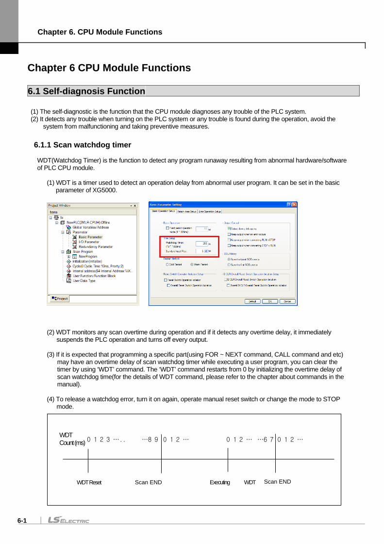
Chapter 6. CPU Module Functions
6-1
Chapter 6 CPU Module Functions
6.1 Self-diagnosis Function (1) The self-diagnostic is the function that the CPU module diagnoses any trouble of the PLC system. (2) It detects any trouble when turning on the PLC system or any trouble is found during the operation, avoid the
system from malfunctioning and taking preventive measures.
6.1.1 Scan watchdog timer WDT(Watchdog Timer) is the function to detect any program runaway resulting from abnormal hardware/software of PLC CPU module.
(1) WDT is a timer used to detect an operation delay from abnormal user program. It can be set in the basic
parameter of XG5000.
(2) WDT monitors any scan overtime during operation and if it detects any overtime delay, it immediately
suspends the PLC operation and turns off every output. (3) If it is expected that programming a specific part(using FOR ~ NEXT command, CALL command and etc)
may have an overtime delay of scan watchdog timer while executing a user program, you can clear the timer by using ‘WDT’ command. The ‘WDT’ command restarts from 0 by initializing the overtime delay of scan watchdog time(for the details of WDT command, please refer to the chapter about commands in the manual).
(4) To release a watchdog error, turn it on again, operate manual reset switch or change the mode to STOP
mode.
0 1 2 3 ….. …8 9
Scan END WDT Reset Executing WDT
0 1 2 … WDT Count (ms) 0 1 2 … …6 7
Scan END
0 1 2 …

Chapter 6. CPU Module Functions
6-2
Caution (1) The setting range of the watchdog timer is 1 ~ 999ms(1ms step), and the initial value is 200ms. (2) If the cycle is set too short, scan watchdog time error may occur if the scan time is elongated by communication traffic overload, etc. It is recommended to set the cycle sufficiently longer that _SCAN_MAX
Chapter 6. CPU Module Functions
6-3
6.1.2 I/O Module Check Function This function checks the I/O module when entering Run mode or during PLC operation (1) When entering Run mode, check if a module disagrees with the parameter setting or in failure (E030) (2) Check if the I/O module is isolated or failed during operation (E031)
If an abnormality is detected, the error indicator lamp (ERR LED) turns on, error number is indicated on the status indicator, and the CPU stops operation.
6.1.3 Battery level check The function monitors battery level and detects, if any, low battery level, warning a user of it. At the moment, the warning lamp (BAT) on the front of the CPU module is On. For the details of measures, please refer to “4.3.3 Battery Life”.
6.1.4 Saving error log The CPU module logs, if any, errors so that a user can easily analyze the error and take corrective measures. It saves each error code to the flag area.
Note The results of self-diagnostic check are logged in the flag area. For the details of self-diagnostic and troubleshooting against errors, please refer to 14.5 Error Codes List during CPU Operation of Chapter 13. Troubleshooting.
6.1.5 Troubleshooting
(1) Types of trouble A trouble occurs mainly by the breakage of PLC, system configuration error and abnormal operation results. ‘Trouble’ can be categorized by ‘heavy fault mode’ at which the system stops for the purpose of the system safety and ‘light fault mode’ at which the system warns a user of a trouble and resumes operation. The PLC system may have a trouble by the following causes.
Trouble in the PLC hardware System configuration error Operation error while a user program is operating Error detection resulting from a fault external device
(2) Operation mode when a trouble is found If a trouble is detected, the PLC system logs the trouble message and stops or resumes operation depending on a trouble mode. (a) Trouble in the PLC hardware
If heavy fault that the PLC may not properly work, such as CPU module, power module and others occurs, the system stops. However, the system resumes operation in case of light fault such as abnormal battery.
(b) System configuration error
It occurs when the hardware structure of PLC is not same as defined in the software. At the moment, the system stops. This occurs at module type disagreement error, module isolated error, or when the I/O mounted on the PLC differs from the I/O set up in the XG5000.
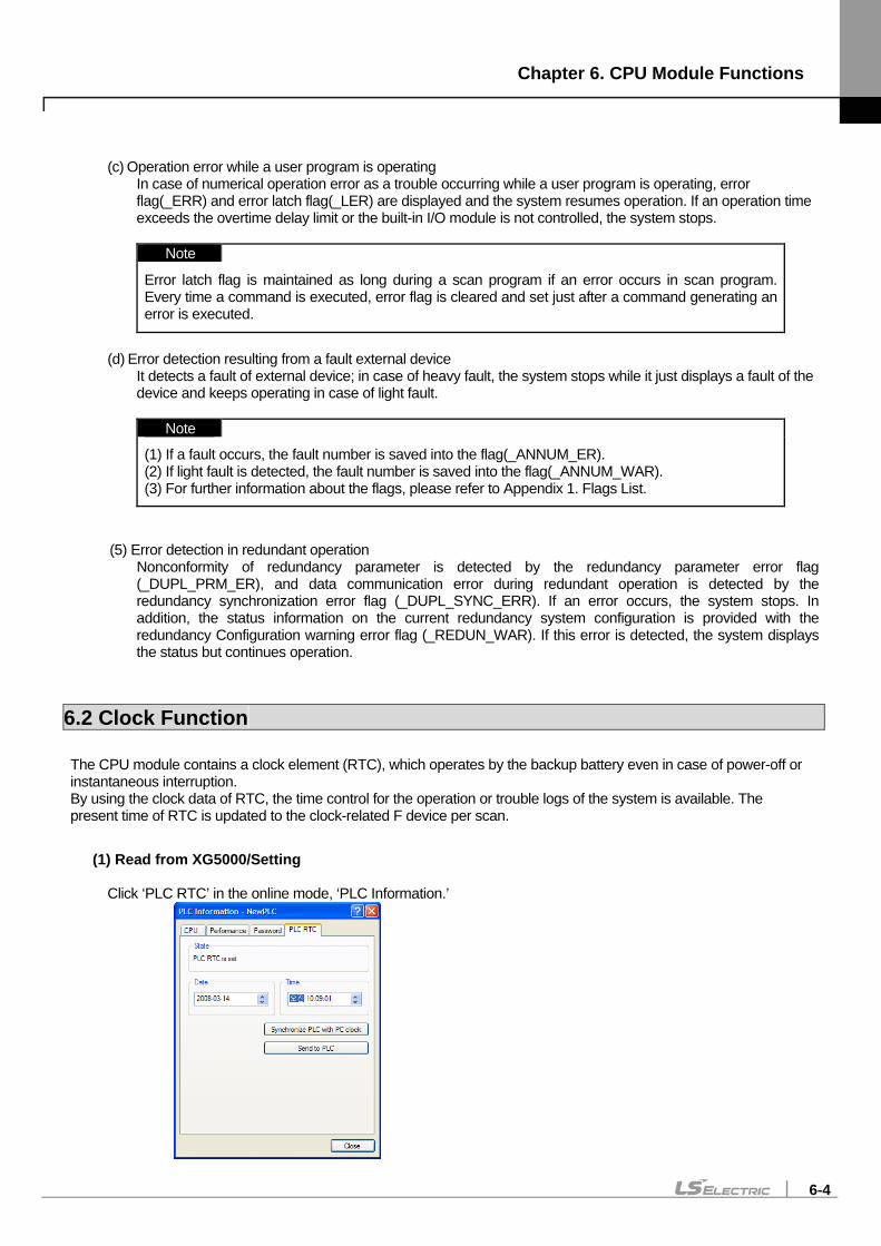
Chapter 6. CPU Module Functions
6-4
(c) Operation error while a user program is operating In case of numerical operation error as a trouble occurring while a user program is operating, error flag(_ERR) and error latch flag(_LER) are displayed and the system resumes operation. If an operation time exceeds the overtime delay limit or the built-in I/O module is not controlled, the system stops.
Note
Error latch flag is maintained as long during a scan program if an error occurs in scan program. Every time a command is executed, error flag is cleared and set just after a command generating an error is executed.
(d) Error detection resulting from a fault external device
It detects a fault of external device; in case of heavy fault, the system stops while it just displays a fault of the device and keeps operating in case of light fault.
Note
(1) If a fault occurs, the fault number is saved into the flag(_ANNUM_ER). (2) If light fault is detected, the fault number is saved into the flag(_ANNUM_WAR). (3) For further information about the flags, please refer to Appendix 1. Flags List.
(5) Error detection in redundant operation Nonconformity of redundancy parameter is detected by the redundancy parameter error flag (_DUPL_PRM_ER), and data communication error during redundant operation is detected by the redundancy synchronization error flag (_DUPL_SYNC_ERR). If an error occurs, the system stops. In addition, the status information on the current redundancy system configuration is provided with the redundancy Configuration warning error flag (_REDUN_WAR). If this error is detected, the system displays the status but continues operation.
6.2 Clock Function The CPU module contains a clock element (RTC), which operates by the backup battery even in case of power-off or instantaneous interruption. By using the clock data of RTC, the time control for the operation or trouble logs of the system is available. The present time of RTC is updated to the clock-related F device per scan.
(1) Read from XG5000/Setting Click ‘PLC RTC’ in the online mode, ‘PLC Information.’
Chapter 6. CPU Module Functions
6-5
It displays the time from the PLC RTC. If it displays the present time incorrectly, a user can fix it up by transferring the right time after manually setting the time or performing “Synchronize PLC with PC clock” method to transmit the time of PC clock connected to the PLC.
(2) Clock reading by Flag It can be monitored by flags as follows.
Flags Examples Size F area Description
_RTC_TIME[0] 16#08 BYTE %FB12 Current time [year, last two digits]
_RTC_TIME[1] 16#02 BYTE %FB13 Current time [Month]
_RTC_TIME[2] 16#23 BYTE %FB14 Current time [Date]
_RTC_TIME[3] 16#14 BYTE %FB15 Current time [Hour]
_RTC_TIME[4] 16#16 BYTE %FB16 Current time [Minute]
_RTC_TIME[5] 16#17 BYTE %FB17 Current time [Second]
_RTC_TIME[6] 16#06 BYTE %FB18 Current time[day]
_RTC_TIME[7] 16#20 BYTE %FB19 Current time [hundred year]
(3) Clock data modified by program A user also can set the value of clock by using a program. It is used when setting the time manually by external digital switches or creating a system to calibrate a clock periodically on network. Input a value into the below flag area and use the ‘_RTC_TIME_USER’ function block. The time data is updated in scan END.
Flags Examples Size F area Description
_RTC_TIME_USER[0] 16#08 BYTE %FB3860 Current time [year, last two digits]
_RTC_TIME_USER [1] 16#02 BYTE %FB3861 Current time [Month]
_RTC_TIME_USER [2] 16#23 BYTE %FB3862 Current time [Date]
_RTC_TIME_USER [3] 16#14 BYTE %FB3863 Current time [Hour]
_RTC_TIME_USER [4] 16#16 BYTE %FB3864 Current time [Minute]
_RTC_TIME_USER [5] 16#17 BYTE %FB3865 Current time [Second]
_RTC_TIME_USER [6] 16#06 BYTE %FB3866 Current time[day]
_RTC_TIME_USER [7] 16#20 BYTE %FB3867 Current time [hundred year] Alternatively, instead of using function blocks, it is also possible to enter clock data into the above area and turn on ‘_RTC_WR’ in order to input the time.
(a) No input is allowed unless time data is entered in a right format (However, even if the day of the week data is not correct, it is set without error detected)
(b) After writing the clock data, check whether it is rightly set by monitoring Reading Clock device.
Chapter 6. CPU Module Functions
6-6
(4) How to express the day of the week
Number 0 1 2 3 4 5 6 Day Sunday Monday Tuesday Wednesday Thursday Friday Saturday
(5) Time error The error of RTC varies depending on the operating temperature. The following table shows the time error for a day.
Operating temp. Max. error (sec/date) Ordinary (sec/date) 0 °C - 4.67 ~ 1.38 -1.46 25 °C - 1.64 ~ 2.42 0.43 55 °C - 5.79 ~ 0.78 -2.29
Caution (1) Initially, RTC may not have any clock data. (2) When using the CPU module, first make sure to set the accurate clock data. (3) If any data out of the clock data range is written into RTC, it does not work properly.
i.e.) 14M 32D 25H (4) RTC may stop or have an error due to abnormal battery and other causes. The error is released if a new
clock data is written. (5) For further information of how to modify the clock data, please refer to the description of XGI commands (6) In the sybchronization of the master and backu CPUs, time difference may occur between the master and
backup.
Chapter 6. CPU Module Functions
6-7
6.3 Remote Function
The operation mode of the CPU can be changed by communication, in addition to the key switch on the module. For remote operation, set the key switch of the CPU module to REM (remote) position>
(1) Types of remote operation (a) Operation by connecting to XG5000 via USB or RS-232C port installed on the CPU module (b) Operate by connecting XG5000 via the USB port on the expansion drive module (c) Other PLC networked on the PLC can be controlled with the CPU module connected to XG5000. (d) The PLC operation is controlled by HMI software and other applications through the dedicated communication.
(2) Remote RUN/STOP (a) Remote RUN/STOP is the function to execute RUN/STOP remotely with the dip switch of the CPU module
set to REMOTE and the RUN/STOP switch set to STOP. (b) It is a very convenient function when the CPU module is located in a place hard to control or in case the
CPU module is to run/stop from the outside.
(3) DEBUG (a) DEBUG is the function to control DEBUG with the dip switch of the CPU module set to REMOTE and
RUN/STOP switch set to STOP. (b) It is a very convenient function when checking program execution status or data in the debugging operation
of the system.
(4) Remote Reset
(a) Remote reset is the function to reset the CPU module remotely in case an error occurs in a place not to directly control the CPU module.
(b) Like the switch control, it supports ‘Reset’ and ‘Overall Reset.’
Note For the further information about remote functions, please refer to the ‘Online’ part in the user’s manual of XG5000.
(5) Flash memory operation mode (a) What is the flash operation mode? It means that the system operates by the backup program in flash in
case the program in ram is damaged. If selecting “Flash Memory Operation Mode”, it starts operation after program in flash moves to the program memory of the CPU module when the operation mode is changed from other mode to RUN mode or when restarting.
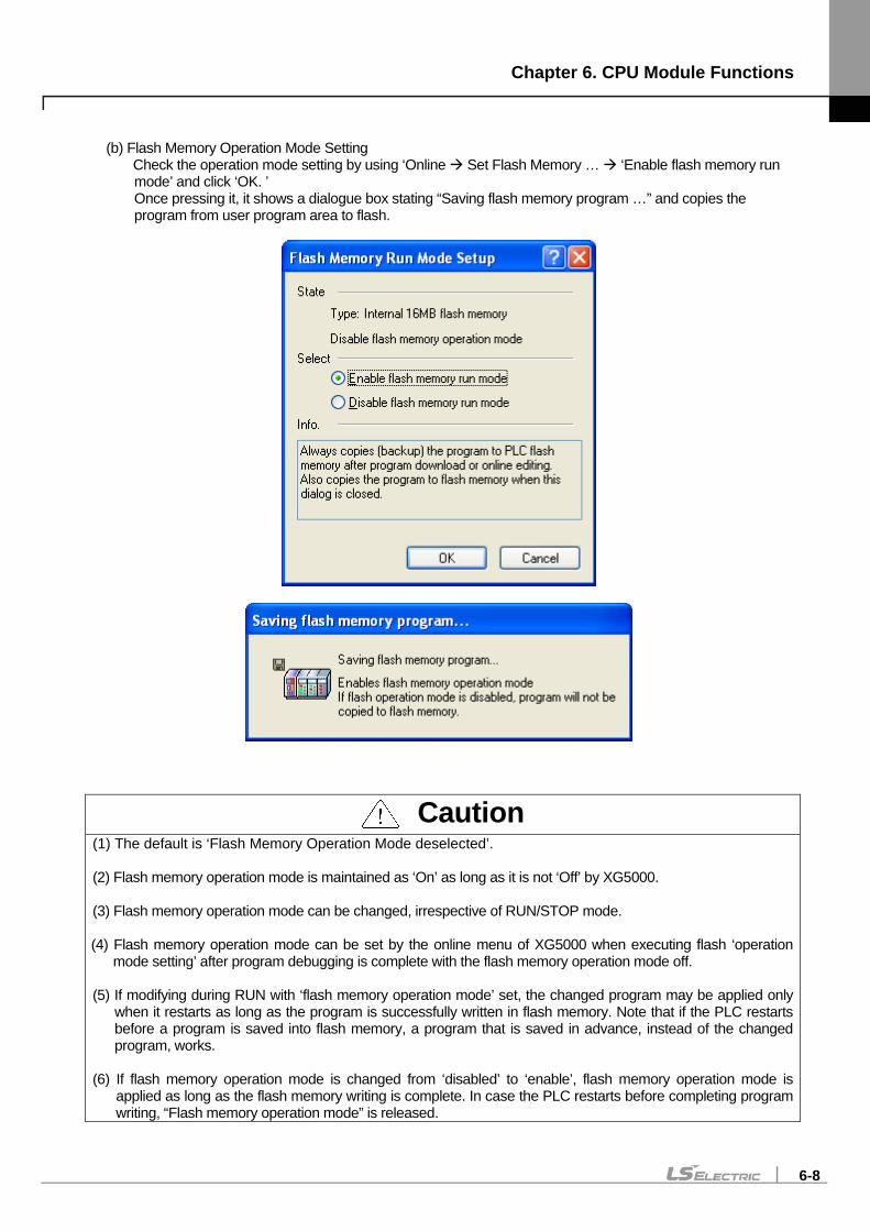
Chapter 6. CPU Module Functions
6-8
(b) Flash Memory Operation Mode Setting Check the operation mode setting by using ‘Online Set Flash Memory … ‘Enable flash memory run
mode’ and click ‘OK. ’ Once pressing it, it shows a dialogue box stating “Saving flash memory program …” and copies the program from user program area to flash.
Caution (1) The default is ‘Flash Memory Operation Mode deselected’. (2) Flash memory operation mode is maintained as ‘On’ as long as it is not ‘Off’ by XG5000. (3) Flash memory operation mode can be changed, irrespective of RUN/STOP mode. (4) Flash memory operation mode can be set by the online menu of XG5000 when executing flash ‘operation
mode setting’ after program debugging is complete with the flash memory operation mode off. (5) If modifying during RUN with ‘flash memory operation mode’ set, the changed program may be applied only
when it restarts as long as the program is successfully written in flash memory. Note that if the PLC restarts before a program is saved into flash memory, a program that is saved in advance, instead of the changed program, works.
(6) If flash memory operation mode is changed from ‘disabled’ to ‘enable’, flash memory operation mode is
applied as long as the flash memory writing is complete. In case the PLC restarts before completing program writing, “Flash memory operation mode” is released.
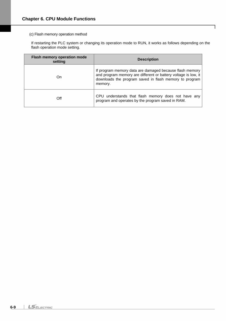
Chapter 6. CPU Module Functions
6-9
(c) Flash memory operation method
If restarting the PLC system or changing its operation mode to RUN, it works as follows depending on the flash operation mode setting.
Flash memory operation mode
setting Description
On
If program memory data are damaged because flash memory and program memory are different or battery voltage is low, it downloads the program saved in flash memory to program memory.
Off CPU understands that flash memory does not have any program and operates by the program saved in RAM.
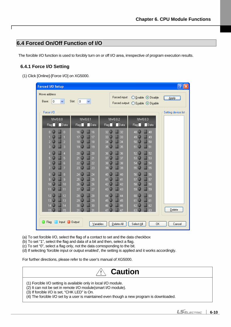
Chapter 6. CPU Module Functions
6-10
6.4 Forced On/Off Function of I/O The forcible I/O function is used to forcibly turn on or off I/O area, irrespective of program execution results.
6.4.1 Force I/O Setting (1) Click [Online]-[Force I/O] on XG5000.
(a) To set forcible I/O, select the flag of a contact to set and the data checkbox (b) To set “1”, select the flag and data of a bit and then, select a flag. (c) To set “0”, select a flag only, not the data corresponding to the bit. (d) If selecting ‘forcible input or output enabled’, the setting is applied and it works accordingly. For further directions, please refer to the user’s manual of XG5000.
Caution (1) Forcible I/O setting is available only in local I/O module.
(2) It can not be set in remote I/O module(smart I/O module). (3) If forcible I/O is set, “CHK LED” is On. (4) The forcible I/O set by a user is maintained even though a new program is downloaded.
Chapter 6. CPU Module Functions
6-11
6.4.2 The point of time of method of forced On/Off process (1) Forcible input
‘Input’ replaces the data of a contact set by Forcible On/Off from the data read from input module at the time of input refresh with the forcibly set data and updates input image area. Therefore, a user program can execute operation with actual input data and forcibly set data.
(2) Forcible output ‘Output’ replaces the data of a contact set by Forcible On/Off from the output image area data containing operation result at the time of output refresh with the forcibly set data and outputs to an output module after completing user program operation. Unlike input, the data in output image area is not changed by forcible On/Off setting.
Caution Cautions for using forcible I/O (1) It works from the time when input/output are set to ‘enable/disable’ respectively after setting forcible data. (2) Forcible input can be set even though actual I/O module is not installed. (3) The previously set On/Off setting data are kept in the CPU module, despite of power off on, operation
mode change, program download or manipulation by reset key. However, it is deleted if overall reset is executed.
(4) Forcible I/O data are not deleted even in STOP mode. (5) To set new data from the first, release every setting of I/O by using ‘overall reset’.
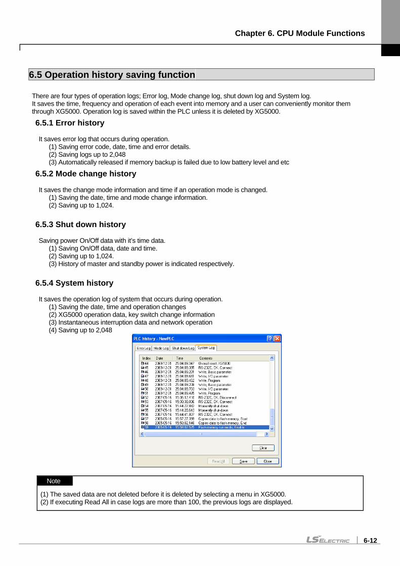
Chapter 6. CPU Module Functions
6-12
6.5 Operation history saving function There are four types of operation logs; Error log, Mode change log, shut down log and System log. It saves the time, frequency and operation of each event into memory and a user can conveniently monitor them through XG5000. Operation log is saved within the PLC unless it is deleted by XG5000.
6.5.1 Error history
It saves error log that occurs during operation. (1) Saving error code, date, time and error details. (2) Saving logs up to 2,048 (3) Automatically released if memory backup is failed due to low battery level and etc
6.5.2 Mode change history
It saves the change mode information and time if an operation mode is changed. (1) Saving the date, time and mode change information. (2) Saving up to 1,024.
6.5.3 Shut down history
Saving power On/Off data with it’s time data. (1) Saving On/Off data, date and time. (2) Saving up to 1,024. (3) History of master and standby power is indicated respectively.
6.5.4 System history
It saves the operation log of system that occurs during operation. (1) Saving the date, time and operation changes (2) XG5000 operation data, key switch change information (3) Instantaneous interruption data and network operation (4) Saving up to 2,048
Note
(1) The saved data are not deleted before it is deleted by selecting a menu in XG5000. (2) If executing Read All in case logs are more than 100, the previous logs are displayed.
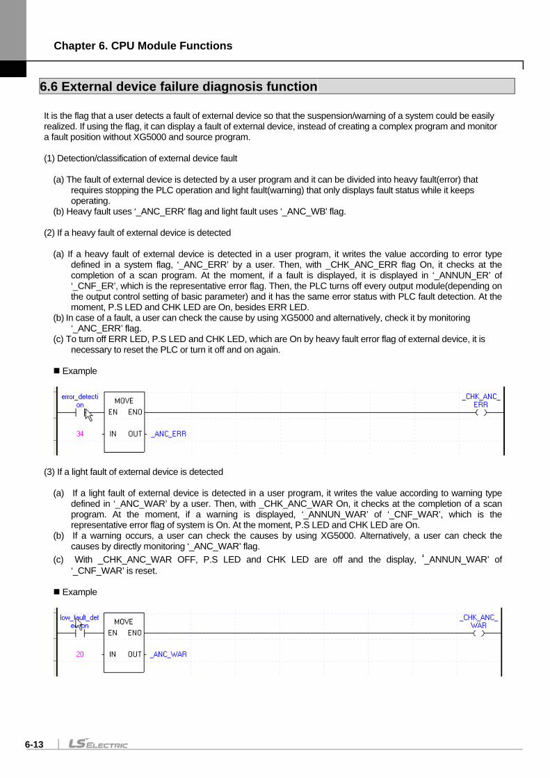
Chapter 6. CPU Module Functions
6-13
6.6 External device failure diagnosis function It is the flag that a user detects a fault of external device so that the suspension/warning of a system could be easily realized. If using the flag, it can display a fault of external device, instead of creating a complex program and monitor a fault position without XG5000 and source program. (1) Detection/classification of external device fault
(a) The fault of external device is detected by a user program and it can be divided into heavy fault(error) that
requires stopping the PLC operation and light fault(warning) that only displays fault status while it keeps operating.
(b) Heavy fault uses ‘_ANC_ERR' flag and light fault uses ‘_ANC_WB' flag.
(2) If a heavy fault of external device is detected (a) If a heavy fault of external device is detected in a user program, it writes the value according to error type
defined in a system flag, ‘_ANC_ERR’ by a user. Then, with _CHK_ANC_ERR flag On, it checks at the completion of a scan program. At the moment, if a fault is displayed, it is displayed in ‘_ANNUN_ER’ of ‘_CNF_ER’, which is the representative error flag. Then, the PLC turns off every output module(depending on the output control setting of basic parameter) and it has the same error status with PLC fault detection. At the moment, P.S LED and CHK LED are On, besides ERR LED.
(b) In case of a fault, a user can check the cause by using XG5000 and alternatively, check it by monitoring ‘_ANC_ERR’ flag.
(c) To turn off ERR LED, P.S LED and CHK LED, which are On by heavy fault error flag of external device, it is necessary to reset the PLC or turn it off and on again.
Example
(3) If a light fault of external device is detected (a) If a light fault of external device is detected in a user program, it writes the value according to warning type
defined in ‘_ANC_WAR’ by a user. Then, with _CHK_ANC_WAR On, it checks at the completion of a scan program. At the moment, if a warning is displayed, ‘_ANNUN_WAR’ of ‘_CNF_WAR’, which is the representative error flag of system is On. At the moment, P.S LED and CHK LED are On.
(b) If a warning occurs, a user can check the causes by using XG5000. Alternatively, a user can check the causes by directly monitoring ‘_ANC_WAR’ flag.
(c) With _CHK_ANC_WAR OFF, P.S LED and CHK LED are off and the display, ‘_ANNUN_WAR’ of ‘_CNF_WAR’ is reset.
Example
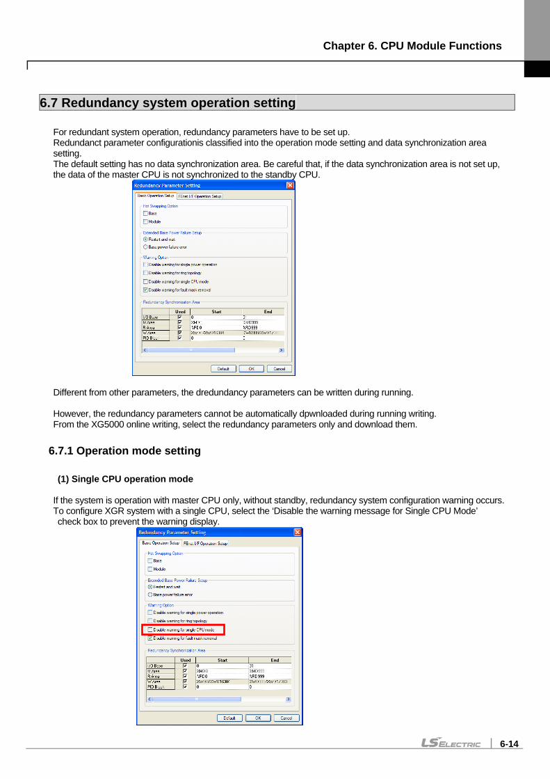
Chapter 6. CPU Module Functions
6-14
6.7 Redundancy system operation setting For redundant system operation, redundancy parameters have to be set up. Redundanct parameter configurationis classified into the operation mode setting and data synchronization area setting. The default setting has no data synchronization area. Be careful that, if the data synchronization area is not set up, the data of the master CPU is not synchronized to the standby CPU.
Different from other parameters, the dredundancy parameters can be written during running. However, the redundancy parameters cannot be automatically dpwnloaded during running writing. From the XG5000 online writing, select the redundancy parameters only and download them.
6.7.1 Operation mode setting
(1) Single CPU operation mode If the system is operation with master CPU only, without standby, redundancy system configuration warning occurs. To configure XGR system with a single CPU, select the ‘Disable the warning message for Single CPU Mode’ check box to prevent the warning display.
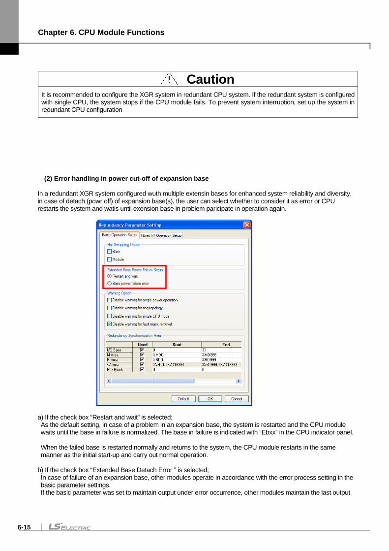
Chapter 6. CPU Module Functions
6-15
(2) Error handling in power cut-off of expansion base In a redundant XGR system configured wuth multiple extensin bases for enhanced system reliability and diversity, in case of detach (powr off) of expansion base(s), the user can select whether to consider it as error or CPU restarts the system and watis until exension base in problem paricipate in operation again.
a) If the check box “Restart and wait” is selected; As the default setting, in case of a problem in an expansion base, the system is restarted and the CPU module waits until the base in failure is normalized. The base in failure is indicated with “Ebxx” in the CPU indicator panel.
When the failed base is restarted normally and returns to the system, the CPU module restarts in the same manner as the initial start-up and carry out normal operation.
b) If the check box “Extended Base Detach Error ” is selected; In case of failure of an expansion base, other modules operate in accordance with the error process setting in the basic parameter settings. If the basic parameter was set to maintain output under error occurrence, other modules maintain the last output.
Caution It is recommended to configure the XGR system in redundant CPU system. If the redundant system is configured with single CPU, the system stops if the CPU module fails. To prevent system interruption, set up the system in redundant CPU configuration
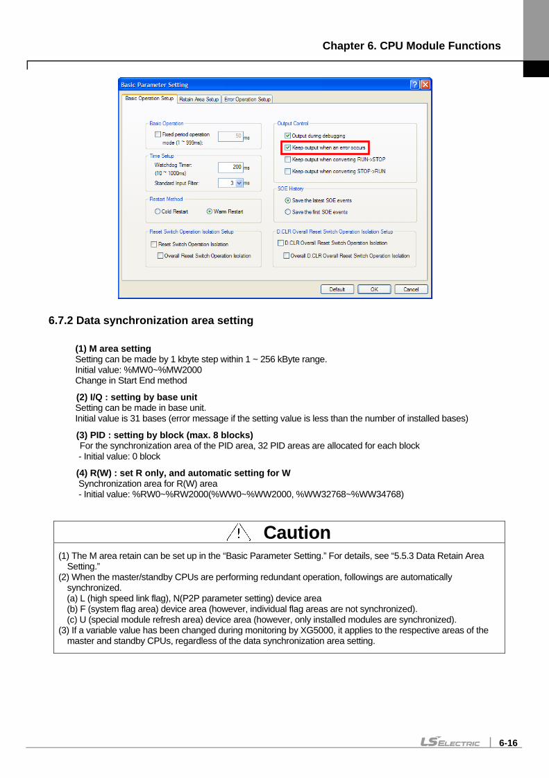
Chapter 6. CPU Module Functions
6-16
6.7.2 Data synchronization area setting
(1) M area setting Setting can be made by 1 kbyte step within 1 ~ 256 kByte range. Initial value: %MW0~%MW2000 Change in Start End method
(2) I/Q : setting by base unit Setting can be made in base unit. Initial value is 31 bases (error message if the setting value is less than the number of installed bases)
(3) PID : setting by block (max. 8 blocks) For the synchronization area of the PID area, 32 PID areas are allocated for each block
- Initial value: 0 block
(4) R(W) : set R only, and automatic setting for W Synchronization area for R(W) area - Initial value: %RW0~%RW2000(%WW0~%WW2000, %WW32768~%WW34768)
Caution (1) The M area retain can be set up in the “Basic Parameter Setting.” For details, see “5.5.3 Data Retain Area Setting.”
(2) When the master/standby CPUs are performing redundant operation, followings are automatically synchronized.
(a) L (high speed link flag), N(P2P parameter setting) device area (b) F (system flag area) device area (however, individual flag areas are not synchronized). (c) U (special module refresh area) device area (however, only installed modules are synchronized). (3) If a variable value has been changed during monitoring by XG5000, it applies to the respective areas of the master and standby CPUs, regardless of the data synchronization area setting.
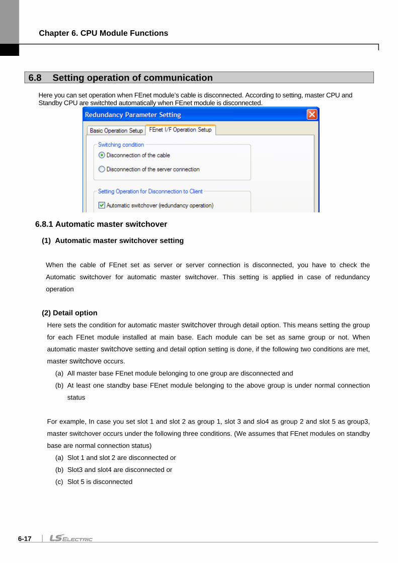
Chapter 6. CPU Module Functions
6-17
6.8 Setting operation of communication Here you can set operation when FEnet module’s cable is disconnected. According to setting, master CPU and Standby CPU are switchted automatically when FEnet module is disconnected.
6.8.1 Automatic master switchover
(1) Automatic master switchover setting
When the cable of FEnet set as server or server connection is disconnected, you have to check the
Automatic switchover for automatic master switchover. This setting is applied in case of redundancy
operation
(2) Detail option Here sets the condition for automatic master switchover through detail option. This means setting the group
for each FEnet module installed at main base. Each module can be set as same group or not. When
automatic master switchove setting and detail option setting is done, if the following two conditions are met,
master switchove occurs.
(a) All master base FEnet module belonging to one group are disconnected and
(b) At least one standby base FEnet module belonging to the above group is under normal connection
status
For example, In case you set slot 1 and slot 2 as group 1, slot 3 and slo4 as group 2 and slot 5 as group3,
master switchover occurs under the following three conditions. (We assumes that FEnet modules on standby
base are normal connection status)
(a) Slot 1 and slot 2 are disconnected or
(b) Slot3 and slot4 are disconnected or
(c) Slot 5 is disconnected
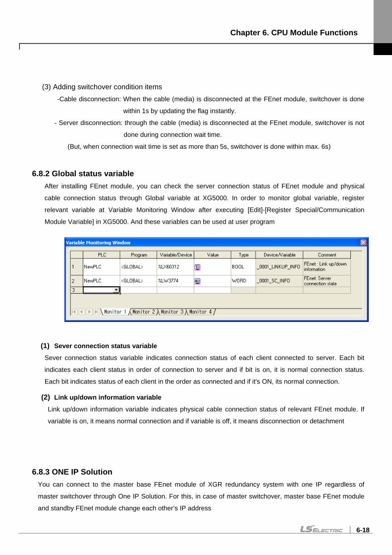
Chapter 6. CPU Module Functions
6-18
(3) Adding switchover condition items
-Cable disconnection: When the cable (media) is disconnected at the FEnet module, switchover is done
within 1s by updating the flag instantly.
- Server disconnection: through the cable (media) is disconnected at the FEnet module, switchover is not
done during connection wait time.
(But, when connection wait time is set as more than 5s, switchover is done within max. 6s)
6.8.2 Global status variable After installing FEnet module, you can check the server connection status of FEnet module and physical
cable connection status through Global variable at XG5000. In order to monitor global variable, register
relevant variable at Variable Monitoring Window after executing [Edit]-[Register Special/Communication
Module Variable] in XG5000. And these variables can be used at user program
(1) Sever connection status variable Sever connection status variable indicates connection status of each client connected to server. Each bit
indicates each client status in order of connection to server and if bit is on, it is normal connection status.
Each bit indicates status of each client in the order as connected and if it's ON, its normal connection.
(2) Link up/down information variable Link up/down information variable indicates physical cable connection status of relevant FEnet module. If
variable is on, it means normal connection and if variable is off, it means disconnection or detachment
6.8.3 ONE IP Solution You can connect to the master base FEnet module of XGR redundancy system with one IP regardless of
master switchover through One IP Solution. For this, in case of master switchover, master base FEnet module
and standby FEnet module change each other’s IP address
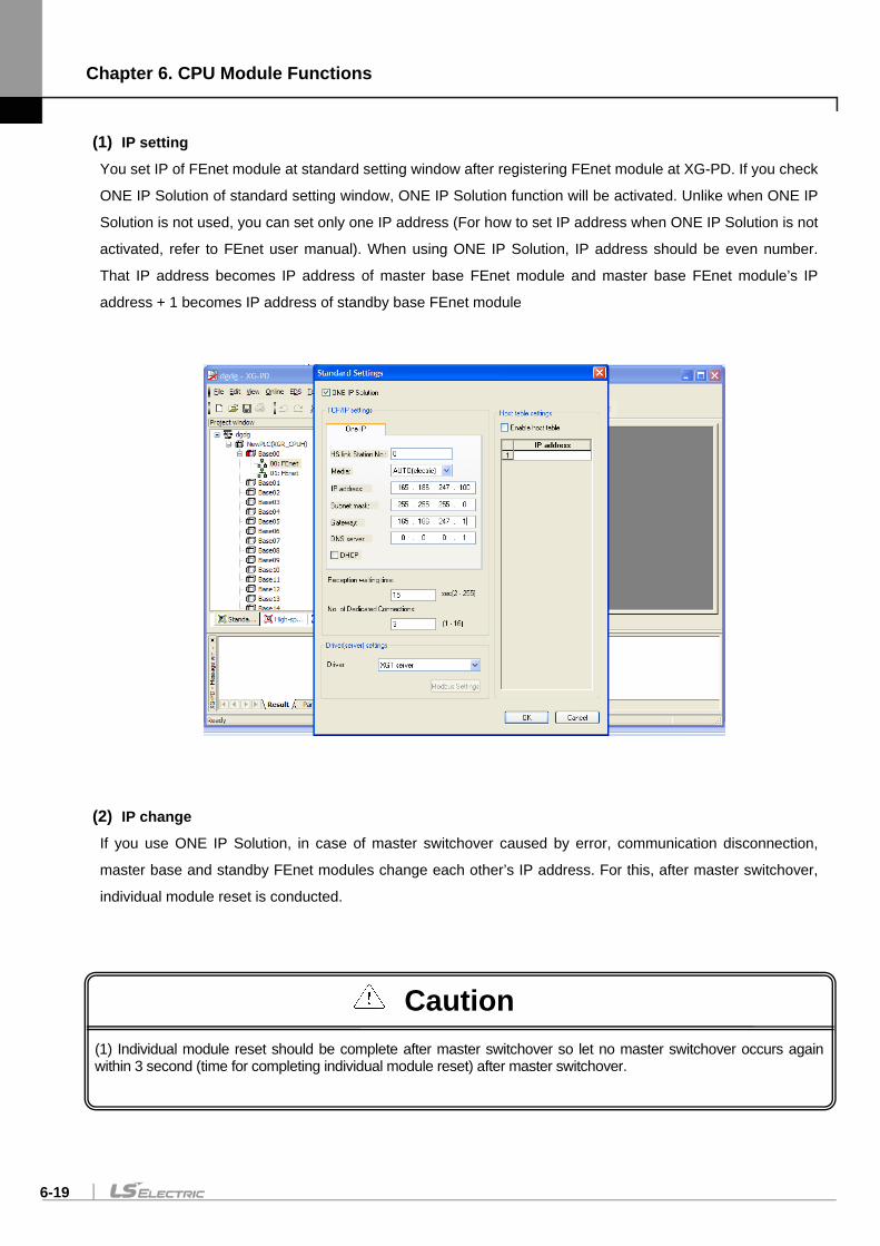
Chapter 6. CPU Module Functions
6-19
(1) IP setting You set IP of FEnet module at standard setting window after registering FEnet module at XG-PD. If you check
ONE IP Solution of standard setting window, ONE IP Solution function will be activated. Unlike when ONE IP
Solution is not used, you can set only one IP address (For how to set IP address when ONE IP Solution is not
activated, refer to FEnet user manual). When using ONE IP Solution, IP address should be even number.
That IP address becomes IP address of master base FEnet module and master base FEnet module’s IP
address + 1 becomes IP address of standby base FEnet module
(2) IP change If you use ONE IP Solution, in case of master switchover caused by error, communication disconnection,
master base and standby FEnet modules change each other’s IP address. For this, after master switchover,
individual module reset is conducted.
(1) Individual module reset should be complete after master switchover so let no master switchover occurs again within 3 second (time for completing individual module reset) after master switchover.
Caution
Chapter 6. CPU Module Functions
6-20
6.9 Fault Mask Function 6.9.1 Applications and operations
(1) Fault mask helps a program keep operating even though a module is in trouble during operation. A module
designated as fault mask normally works until a fault occurs. (2) If an error occurs on a module on which fault mask is set, the module stops working but the entire system
keeps working. (3) If a fault occurs in a module during operation, the CPU module sets the error flag and “PS LED” on the front is
“On.” The error is displayed when accessing to XG5000.
6.9.2 Fault mask setting (1) Fault mask can be set by the online menu of XG5000. For the details, please refer to the user’s manual of
XG5000. (2) Fault mask setting by a program is not available. You can monitor the fault mask flag with program.
(Refer to appendix1. flag list)
6.9.3 Releasing fault mask Fault mask is released only by the following methods.
(1) Releasing the setting in the online menu of XG5000 (2) Releasing by overall reset (3) Automatically releasing in case memory backup is failed due to low battery level and other causes
Note that the fault mask is not released even in the following cases. (1) Power Off→On (2) Operation mode change (3) Program download (4) Reset key(released only when it is pressed for 3 seconds and longer) (5) Data clear
Caution (1) If releasing fault mask with error flag in the CPU module not cleared although the causes of an error are
eliminated, the system stops. Please check the state of error flag before releasing fault mask flag. (2) To remove an error flag, release it after setting I/O skip in the respective module. For details, see
[XG5000 online help desk >>I/O Skip. (3) In case of XGR-CPU V1.8 or above, if you don’t set fault mask, warning message appears when
connecting CPU via XG5000. In case of XGR-CPU V1.8 or above, “Warning for fault mask removal” option is added at Redundancy parameter.
Chapter 6. CPU Module Functions
6-21
6.10 I/O Module Skip Function
6.10.1 Applications and operations During operation, the I/O module skip function excludes a designated module from the operation. For the designated module, the data update and fault diagnostics of I/O data stops as soon as being designated. It is available when temporarily operating it with the fault excluded.
6.10.2 Setting and processing I/O data (1) It can be set at the unit of I/O module.
(For further information about setting, please refer to the user’s manual of XG5000)
(2) Input(I) image area suspends input refresh, so it maintains the value set before skip setting. However, even in the case, the image manipulation by forcible On/Off is still effective.
(3) The actual output of output module is Off when setting the skip function but it changes depending on a user
program’s operation, irrespective of skip setting. After the skip setting, the output value of output module can not be controlled by forcible On/Off.
(4) The skip function is identically executed even when using I/O function.
6.10.3 Releasing skip function The I/O module skip function is released only by the method of setting.
(1) Releasing by the online menu of XG5000 (2) Releasing by overall reset (3) Automatically releasing in case memory backup is failed due to low battery level and other causes
Note that the fault mask is not released even in the following cases. (1) Power Off→On (2) Operation mode change (3) Program download (4) Reset key(released only when it is pressed for 3 seconds and longer) (5) Data clear
Caution If any fault is found in a module when releasing the skip function, the system may stop. Before releasing the skip function, make sure to release the skip with fault mask set and check the operation of a module.
Chapter 6. CPU Module Functions
6-22
6.11 Base Skip Function
6.11.1 Purpose and outline of the operation Base skip is the function to exclude the designated base from operation during an operation. The excluded base stops all functions from the skip. This function is useful to continue operation by excluding a failed base or replace the base.
6.11.2 Setting method • This setting can be done for each base.
6.11.3 Releasing skip function Base skip can be released by following methods only.
• Selecting XG5000’s [Online >> I/O Skip Setting] menu • Release by Overall Reset • Automatic release at backup memory lost by battery voltage drop, etc.
Note that followings do not release the failure mask; • power Off → On, • operation mode change, • program download, • reset key operation (however, released if pressed for 3 seconds or longer), and • data clear
Caution (1) When expansion driver is detached, all modules in base are automatically initialized. (2) When expansion driver is detached, digital output module operates as set in Output control settings of Basic
parameter. (3) When expansion driver is detached, analog output module operates as set in Output type setting (4) For more detail, refer to each module’s user manual.
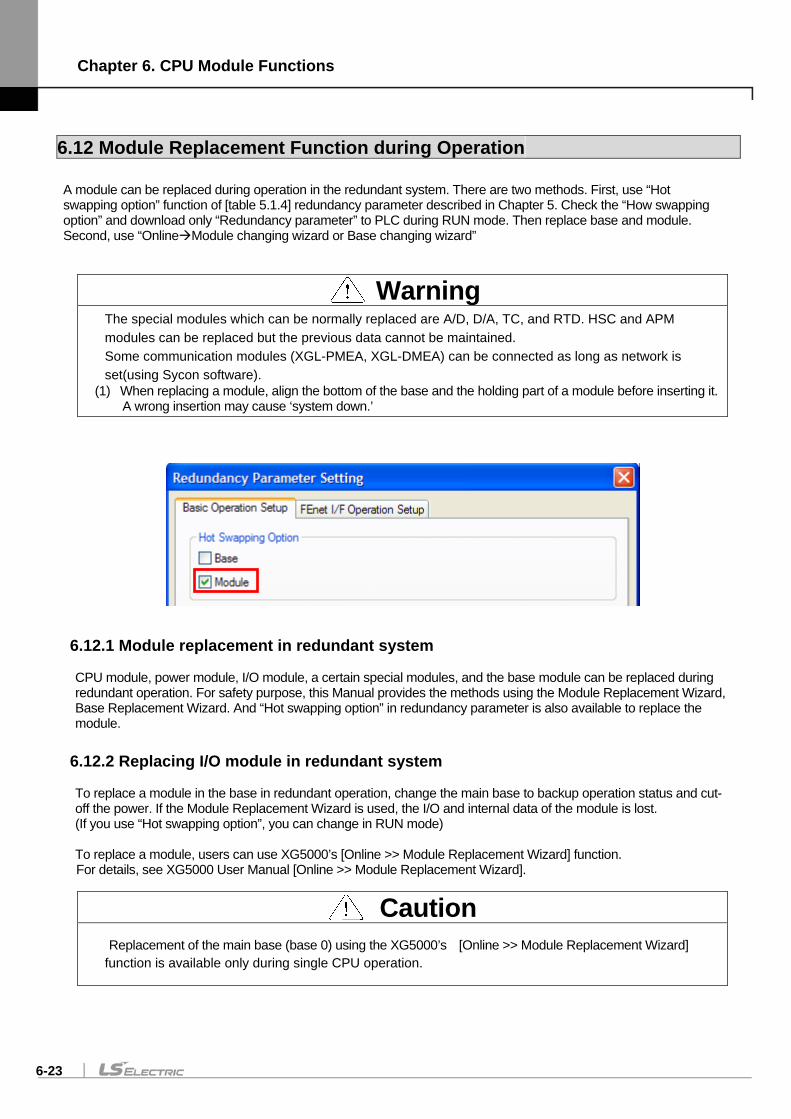
Chapter 6. CPU Module Functions
6-23
6.12 Module Replacement Function during Operation A module can be replaced during operation in the redundant system. There are two methods. First, use “Hot swapping option” function of [table 5.1.4] redundancy parameter described in Chapter 5. Check the “How swapping option” and download only “Redundancy parameter” to PLC during RUN mode. Then replace base and module. Second, use “OnlineModule changing wizard or Base changing wizard”
6.12.1 Module replacement in redundant system
CPU module, power module, I/O module, a certain special modules, and the base module can be replaced during redundant operation. For safety purpose, this Manual provides the methods using the Module Replacement Wizard, Base Replacement Wizard. And “Hot swapping option” in redundancy parameter is also available to replace the module.
6.12.2 Replacing I/O module in redundant system To replace a module in the base in redundant operation, change the main base to backup operation status and cut-off the power. If the Module Replacement Wizard is used, the I/O and internal data of the module is lost. (If you use “Hot swapping option”, you can change in RUN mode) To replace a module, users can use XG5000’s [Online >> Module Replacement Wizard] function. For details, see XG5000 User Manual [Online >> Module Replacement Wizard].
Warning The special modules which can be normally replaced are A/D, D/A, TC, and RTD. HSC and APM modules can be replaced but the previous data cannot be maintained. Some communication modules (XGL-PMEA, XGL-DMEA) can be connected as long as network is set(using Sycon software).
(1) When replacing a module, align the bottom of the base and the holding part of a module before inserting it. A wrong insertion may cause ‘system down.’
Caution Replacement of the main base (base 0) using the XG5000’s [Online >> Module Replacement Wizard]
function is available only during single CPU operation.
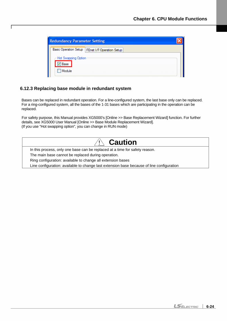
Chapter 6. CPU Module Functions
6-24
6.12.3 Replacing base module in redundant system
Bases can be replaced in redundant operation. For a line-configured system, the last base only can be replaced. For a ring-configured system, all the bases of the 1-31 bases which are participating in the operation can be replaced. For safety purpose, this Manual provides XG5000’s [Online >> Base Replacement Wizard] function. For further details, see XG5000 User Manual [Online >> Base Module Replacement Wizard]. (If you use “Hot swapping option”, you can change in RUN mode)
Caution In this process, only one base can be replaced at a time for safety reason. The main base cannot be replaced during operation. Ring configuration: available to change all extension bases Line configuration: available to change last extension base because of line configuration
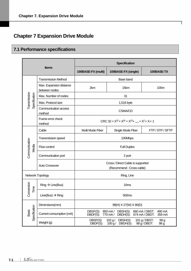
Chapter 7. Expansion Drive Module
7-1
Chapter 7 Expansion Drive Module
7.1 Performance specifications
Items Specification
100BASE-FX (multi) 100BASE-FX (single) 100BASE-TX
Tran
smiss
ion
Spec
ificat
ion
Transmission Method Base band
Max. Expansion distance between nodes
2km 15km 100m
Max. Number of nodes 31
Max. Protocol size 1,516 byte
Communication access method
CSMA/CD
Frame error check method
CRC 32 = X32 + X26 + X23+ ,,,,, + X2 + X + 1
Com
mun
icatio
n M
edia
Cable Multi Mode Fiber Single Mode Fiber FTP / STP / SFTP
Transmission speed 100Mbps
Flow control Full Duplex
Communication port 2 port
Auto Crossover Cross / Direct Cable is supported
(Recommend : Cross cable)
Network Topology Ring, Line
Conv
ersio
n Ti
me Ring Line(Bus) 10ms
Line(Bus) Ring 500ms
Basic
Sp
ecific
atio
n Dimensions(mm) 98(H) X 27(W) X 90(D)
Current consumption (mA) DBSF(S): 850 mA / DBSH(S): 660 mA / DBST: 490 mA DBDF(S): 770 mA / DBDH(S): 674 mA / DBDT: 359 mA
Weight (g) DBSF(S): 102 g / DBSH(S): 101 g / DBST: 99 g DBDF(S): 100 g / DBDH(S): 98 g / DBDT: 98 g
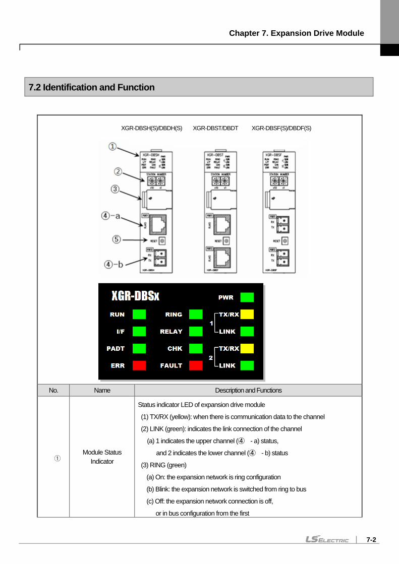
Chapter 7. Expansion Drive Module
7-2
7.2 Identification and Function
No. Name Description and Functions
① Module Status
Indicator
Status indicator LED of expansion drive module
(1) TX/RX (yellow): when there is communication data to the channel
(2) LINK (green): indicates the link connection of the channel
(a) 1 indicates the upper channel (④ - a) status,
and 2 indicates the lower channel (④ - b) status
(3) RING (green)
(a) On: the expansion network is ring configuration
(b) Blink: the expansion network is switched from ring to bus
(c) Off: the expansion network connection is off,
or in bus configuration from the first
XGR-DBSH(S)/DBDH(S) XGR-DBST/DBDT XGR-DBSF(S)/DBDF(S)
Chapter 7. Expansion Drive Module
7-3
(4) RELAY (green)
(a) On: the module neighboring the two channels are connected and conducts
as a data relay
(b) Off: the module neighboring the two channels are connected and does not
conduct as a data relay
(5) CHK (green)
(a) On: indicates CPU’s WAR LED
(b) Blink: station No. in the expansion network conflict (other station numbers)
(6) FAULT (red)
(a) On: network station No. conflict (self station No.)
(b) Blink: frame error occurred
(7) RUN (green)
(a) On: CPU operation mode is RUN
(b) Blink: expansion drive is in wait state for CPU recognition
(c) Off: CPU operation mode is STOP
(8) I/F (green)
(a) Blink: in normal I/F with expansion manager
(b) Off: I/F with expansion manager unavailable
(9) PADT On (green): on in PADT connection (10) ERR On (red): CPU operation mode is ERR
② Base Setting Switch
Switch for setting expansion base No. (1) x10 for 10 digit setting, x1 for 1 digit setting (2) Max. 31 bases can be set up (3) Error LED on at station No. conflict or setting more than 31 station numbers
③ USB Connector Connector for peripheral devices (XG5000 etc.) (USB 1.1 supported)
④ Expansion Network
Connector
Connector for expansion base connection. (1) 2 connectors are provided for ring connection without additional switching device (2) Optical-optical, electrical-electrical, and optical-electrical models are provided to enable network construction using mixed electrical/optical
⑤ Expansion Drive
Module Reset Switch
Pressing this switch will trigger module reset operation. (1) Used to reset module only. (2) Make sure to skip the module before conducting module reset (3) Take care that resetting without skip setting of the respective base will cause module isolation error.

Chapter 7. Expansion Drive Module
7-4
Chapter 8. Power Module
8-1
Chapter 8 Power Module This chapter describes the selection, type and specifications of power module.
8.1 Type and Specification
We provide diverse types according to input voltage and output capacity. Select right module according to environment and system. [Table 8.1.1] Power module specification
Item XGR-AC12 XGR-AC22 XGR-AC13 XGR- AC23 XGR-DC42
Input
Rated input voltage 110 VAC 220 VAC 110 VAC 220 VAC 24 VDC
Input voltage range 85V~132VAC 176V~264VAC 85V~132VAC 176V~264VAC 19.2 ~ 28.8 VDC
Input frequency 50 / 60 Hz (47 ~ 63 Hz) -
Max. input power 110 VA / 42 W 176 VA / 72 W -
Inrush current 20A peak and lower (within8 ) 80A peak and lower
Efficiency 65% or higher
Input fuse Built in(not replaceable by a user) - AC power: 250V / 3.15A ( Time-lag Type ) UL approved - DC power: 125V/10A (Time-lag type) UL approved
Allowed instantaneous interruption
Within 20
Output
Output voltage 5VDC (±2%)
Output current 5.5A 8.5A 7.5A
Output power 27.5W @ 55 46.75W @ 55 37.5W @ 55 Over current protection 6.0 A ~ 13.0 A 9.3 A ~ 17.0 A 9.0 A~17.0 A
Relay Output
Purpose RUN contact (refer to 8.2) Rated switching voltage/current 24VDC, 0.5A
Min. switching load 5VDC, 1
Response time Off→On/ On→Off: 10 and lower/12 and lower
Life Mechanical life: 20 million and more times, electrical life: rated switching current: 100 thousand and more times
Voltage status display LED On when output voltage is normal
Specification of cable 0.75 ~ 2 mm2
Available clamped terminal RAV1.25-3.5, RAV2-3.5
Dimension (W x H x D mm) 55 x 95 x 90 55 x 95 x 110
Weight 326g 382g 334g 384g 417g
Applied base and install position Power part of basic/expansion base Power part of expansion base Power part of
basic/expansion base
Note (1) Allowable instantaneous interruption time
(a) The time that the normal output voltage is maintained(normal operation) when AC110/220V/DC24V input voltage is less
than rating value (AC 85/176V/DC 19.2V) (2) Over current protection
(a) If a current over the rated level is allowed on 5VDC circuit, an over current protective system cuts off the circuit, suspending the system.
(b) If there is any overcurrent, the system should be restarted after eliminating the causes such as low current capacity, short-circuit and etc.
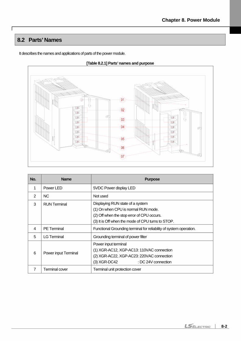
Chapter 8. Power Module
8-2
8.2 Parts’ Names
It describes the names and applications of parts of the power module.
[Table 8.2.1] Parts’ names and purpose
No. Name Purpose
1 Power LED 5VDC Power display LED
2 NC Not used
3 RUN Terminal Displaying RUN state of a system (1) On when CPU is normal RUN mode. (2) Off when the stop error of CPU occurs. (3) It is Off when the mode of CPU turns to STOP.
4 PE Terminal Functional Grounding terminal for reliability of system operation.
5 LG Terminal Grounding terminal of power filter
6 Power input Terminal
Power input terminal (1) XGR-AC12, XGP-AC13: 110VAC connection (2) XGR-AC22, XGP-AC23: 220VAC connection (3) XGR-DC42 : DC 24V connection
7 Terminal cover Terminal unit protection cover
Chapter 8. Power Module
8-3
8.3 Selection The selection of power module is determined by the current that input power voltage and power module should supply to the system, that is, the sum of current consumption of digital I/O module, special module and communication module that are installed on a same base with the power module. If it exceeds the rated output capacity of power module, the system does not properly work. Select a power module by considering the power current of each module when structuring a system.
[Table 8.3.1] Current consumption by modules
Item Name Consumption
current (Unit: mA)
Item Name Consumption
current (Unit: mA)
CPU module XGR-CPUH/T 980
Analog input module
XGF-AV8A 420 XGF-AC8A 420
XGR-CPUH/F 1,310 XGF-AD4S 610
Expansion drive module
XGR-DBST 550 XGF-AD8A 420 XGR-DBSF 550 XGF-AD16A 330 XGR-DBSH 550
Analog output module
XGF-DV4A 190 (250)
DC24V input module
XGI-D21A 20 XGF-DC4A 190 (400) XGI-D22A 30 XGF-DC4S 200 (220) XGI-D22B 30 XGF-DV8A 147 (180) XGI-D24A 50 XGF-DC8A 243 (300) XGI-D24B 50 XGF-DV4S 200 (150) XGI-D28A 60 High speed counter
module XGF-HO2A 270
XGI-D28B 60 XGF-HD2A 330 AC110V input module XGI-A12A 30
Positioning module
XGF-PO3A 400 AC220V input module XGI-A21A 20 XGF-PO2A 360
Relay output module XGQ-RY1A 250 XGF-PO1A 340 XGQ-RY2A 500 XGF-PD3A 860 XGQ-RY2B 500 XGF-PD2A 790
Transistor output module
XGQ-TR2A 70 XGF-PD1A 510 XGQ-TR2B 70 XGF-PO4H 430 XGQ-TR4A 130 XGF-PO3H 420 XGQ-TR4B 130 XGF-PO2H 410 XGQ-TR8A 230 XGF-PO1H 400 XGQ-TR8B 230 XGF-PD4H 890
Triac output module XGQ-SS2A 300 XGF-PD3H 850 XGF-PD2H 600
I/O module XGH-DT4A 110 XGF-PD1H 520
RTD input module XGF-RD4A 450
FEnet I/F module (Optical/Electricity)
XGL-EFMF 640 XGF-RD4S 783
XGL-EFMT 410 Thermocouple input module
XGF-TC4S 610
XGL-ESHF 1,200 Event input module XGF-SOEA 700
PAPIEnet I/F Module XGL-EIMF 490
Motion control module
XGF-M16M 640
XGL-EIMT 335 Analog I/O module XGF-AH6A 770
XGL-EIMH 400
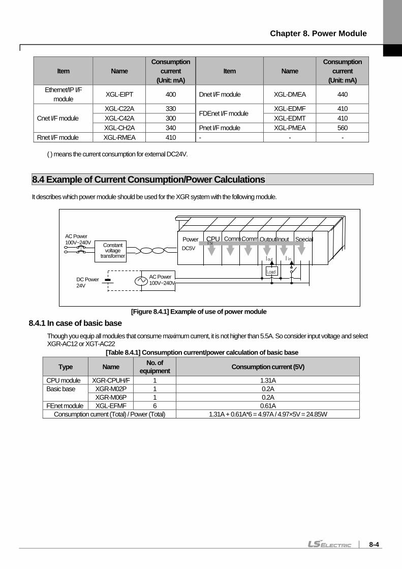
Chapter 8. Power Module
8-4
Item Name Consumption
current (Unit: mA)
Item Name Consumption
current (Unit: mA)
Ethernet/IP I/F module
XGL-EIPT 400 Dnet I/F module XGL-DMEA 440
Cnet I/F module XGL-C22A 330
FDEnet I/F module XGL-EDMF 410
XGL-C42A 300 XGL-EDMT 410 XGL-CH2A 340 Pnet I/F module XGL-PMEA 560
Rnet I/F module XGL-RMEA 410 - - - ( ) means the current consumption for external DC24V.
8.4 Example of Current Consumption/Power Calculations It describes which power module should be used for the XGR system with the following module.
8.4.1 In case of basic base Though you equip all modules that consume maximum current, it is not higher than 5.5A. So consider input voltage and select XGR-AC12 or XGT-AC22
[Table 8.4.1] Consumption current/power calculation of basic base
Type Name No. of equipment Consumption current (5V)
CPU module XGR-CPUH/F 1 1.31A Basic base XGR-M02P 1 0.2A
XGR-M06P 1 0.2A FEnet module XGL-EFMF 6 0.61A
Consumption current (Total) / Power (Total) 1.31A + 0.61A*6 = 4.97A / 4.97×5V = 24.85W
Power CPU Constant voltage
transformer
AC Power 100V~240V Comm. Comm. Output Input Special
DC5V
Load
Iout Iin
I5V
AC Power 100V~240V DC Power
24V
[Figure 8.4.1] Example of use of power module
Chapter 8. Power Module
8-5
8.4.2 In case of expansion base
Calculate the consumption current of module equipped at expansion base and select 5.5A or 8.5A [Table 8.4.2] Consumption current/power calculation of basic base
Type Name No. of equipment Consumption current (5V)
Expansion drive module
XGR-DBSF 1 0.65A
Expansion base XGB-E12RP 1 0.21A Input module XGI-D24A 2 0.05A Output module XGQ-RY2A 6 0.5A A/D conversion module
XGF-AD4S 2 0.61A
Profibus-DP XGL-PMEA 2 0.56A
Consumption current (Total) / Power (Total) 0.65A + 0.21A+0.05A*2 + 0.5A*6 + 0.61A*2 + 0.56A*2 = 6.30A / 6.30A × 5V = 31.50 W
Since total of consumption current (5V) is 6.17A, use one among XGR-AC13, XGP-AC23 according to input voltage. If power module is less than a necessary capacity, reliability of system is not guaranteed.
Note If efficiency of power module is applied to power (5V), the user can estimates the maximum input power of PLC system. Ex) Total of consumption power (5V) / Power module efficiency (Min.) = 100 W / 0.65 % = 154 W

Chapter 8. Power Module
8-6
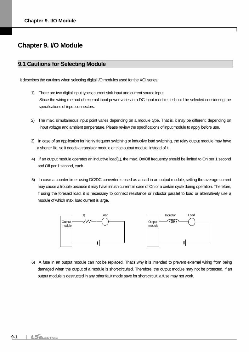
Chapter 9. I/O Module
9-1
Chapter 9. I/O Module
9.1 Cautions for Selecting Module It describes the cautions when selecting digital I/O modules used for the XGI series. 1) There are two digital input types; current sink input and current source input
Since the wiring method of external input power varies in a DC input module, it should be selected considering the specifications of input connectors.
2) The max. simultaneous input point varies depending on a module type. That is, it may be different, depending on
input voltage and ambient temperature. Please review the specifications of input module to apply before use. 3) In case of an application for highly frequent switching or inductive load switching, the relay output module may have
a shorter life, so it needs a transistor module or triac output module, instead of it.
4) If an output module operates an inductive load(L), the max. On/Off frequency should be limited to On per 1 second and Off per 1 second, each.
5) In case a counter timer using DC/DC converter is used as a load in an output module, setting the average current
may cause a trouble because it may have inrush current in case of On or a certain cycle during operation. Therefore, if using the foresaid load, it is necessary to connect resistance or inductor parallel to load or alternatively use a module of which max. load current is large.
6) A fuse in an output module can not be replaced. That’s why it is intended to prevent external wiring from being
damaged when the output of a module is short-circuited. Therefore, the output module may not be protected. If an output module is destructed in any other fault mode save for short-circuit, a fuse may not work.
Output module
R Load
Output module
Inductor Load
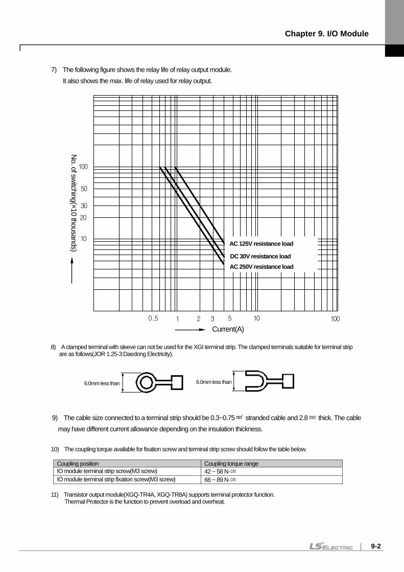
Chapter 9. I/O Module
9-2
7) The following figure shows the relay life of relay output module.
It also shows the max. life of relay used for relay output.
8) A clamped terminal with sleeve can not be used for the XGI terminal strip. The clamped terminals suitable for terminal strip are as follows(JOR 1.25-3:Daedong Electricity).
9) The cable size connected to a terminal strip should be 0.3~0.75 stranded cable and 2.8 thick. The cable may have different current allowance depending on the insulation thickness.
10) The coupling torque available for fixation screw and terminal strip screw should follow the table below.
Coupling position Coupling torque range IO module terminal strip screw(M3 screw) 42 ~ 58 N· IO module terminal strip fixation screw(M3 screw) 66 ~ 89 N·
11) Transistor output module(XGQ-TR4A, XGQ-TR8A) supports terminal protector function. Thermal Protector is the function to prevent overload and overheat.
No. of switching(×10 thousands)
100
50
30
20
10
100 10 5 3 2 1 0.5
Current(A)
DC 30V resistance load
AC 125V resistance load
AC 250V resistance load
6.0mm less than 6.0mm less than
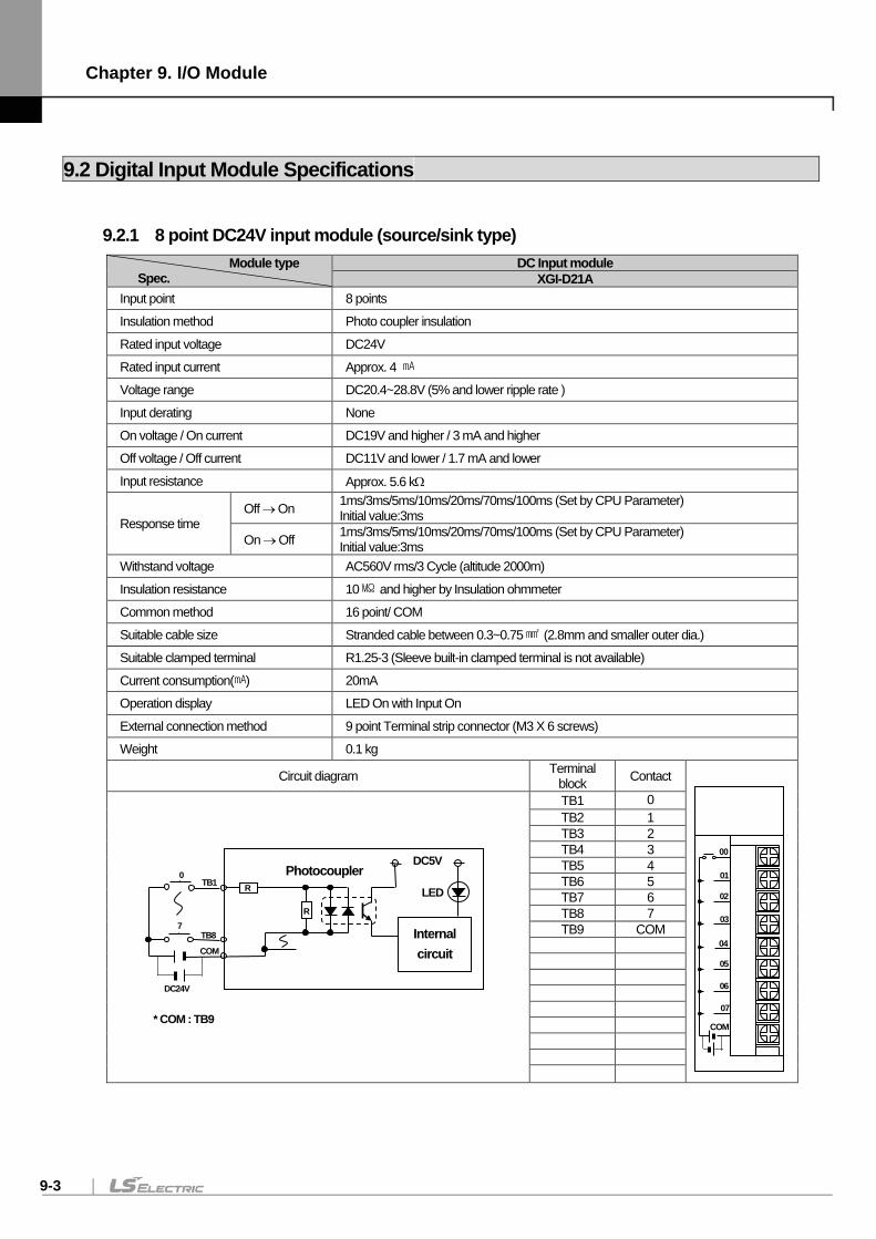
Chapter 9. I/O Module
9-3
9.2 Digital Input Module Specifications
9.2.1 8 point DC24V input module (source/sink type) Module type
Spec. DC Input module
XGI-D21A Input point 8 points
Insulation method Photo coupler insulation
Rated input voltage DC24V
Rated input current Approx. 4
Voltage range DC20.4~28.8V (5% and lower ripple rate )
Input derating None
On voltage / On current DC19V and higher / 3 mA and higher
Off voltage / Off current DC11V and lower / 1.7 mA and lower
Input resistance Approx. 5.6 kΩ
Response time Off → On 1ms/3ms/5ms/10ms/20ms/70ms/100ms (Set by CPU Parameter)
Initial value:3ms
On → Off 1ms/3ms/5ms/10ms/20ms/70ms/100ms (Set by CPU Parameter) Initial value:3ms
Withstand voltage AC560V rms/3 Cycle (altitude 2000m)
Insulation resistance 10 and higher by Insulation ohmmeter
Common method 16 point/ COM
Suitable cable size Stranded cable between 0.3~0.75 (2.8mm and smaller outer dia.)
Suitable clamped terminal R1.25-3 (Sleeve built-in clamped terminal is not available)
Current consumption() 20mA
Operation display LED On with Input On
External connection method 9 point Terminal strip connector (M3 X 6 screws)
Weight 0.1 kg
Circuit diagram Terminal block Contact
TB1 0 TB2 1 TB3 2 TB4 3 TB5 4 TB6 5 TB7 6 TB8 7 TB9 COM
DC24V
Internal circuit
R
7
0
TB1
COM
Photocoupler
TB8
R
* COM : TB9
DC5V
LED
00
01
02
03
04
05
06
07
COM
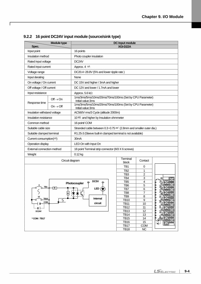
Chapter 9. I/O Module
9-4
9.2.2 16 point DC24V input module (source/sink type) Module type
Spec. DC Input module
XGI-D22A Input point 16 points
Insulation method Photo coupler insulation
Rated input voltage DC24V
Rated input current Approx. 4
Voltage range DC20.4~28.8V (5% and lower ripple rate )
Input derating None
On voltage / On current DC 15V and higher / 3mA and higher
Off voltage / Off current DC 12V and lower / 1.7mA and lower
Input resistance Approx. 5.6 kΩ
Response time Off → On 1ms/3ms/5ms/10ms/20ms/70ms/100ms (Set by CPU Parameter)
Initial value:3ms
On → Off 1ms/3ms/5ms/10ms/20ms/70ms/100ms (Set by CPU Parameter) Initial value:3ms
Insulation withstand voltage AC560V rms/3 Cycle (altitude 2000m)
Insulation resistance 10 and higher by Insulation ohmmeter
Common method 16 point/ COM
Suitable cable size Stranded cable between 0.3~0.75 (2.8mm and smaller outer dia.)
Suitable clamped terminal R1.25-3 (Sleeve built-in clamped terminal is not available)
Current consumption() 30mA
Operation display LED On with Input On
External connection method 18 point Terminal strip connector (M3 X 6 screws)
Weight 0.12 kg
Circuit diagram Terminal block Contact
TB1 0 TB2 1 TB3 2 TB4 3 TB5 4 TB6 5 TB7 6 TB8 7 TB9 8 TB10 9 TB11 10 TB12 11 TB13 12 TB14 13 TB15 14 TB16 15 TB17 COM TB18 NC
00 01 02
03 04
05 06
07 08
09 10
11 12
13 14
15 COM
DC24V
Internal circuit
R
15
0
TB1
COM
Photocoupler
TB16
R
* COM : TB17
DC5V
LED
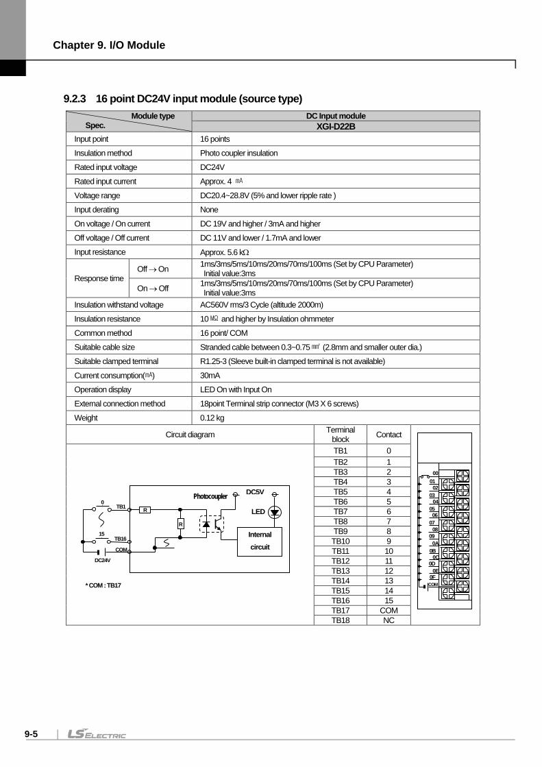
Chapter 9. I/O Module
9-5
9.2.3 16 point DC24V input module (source type) Module type
Spec. DC Input module
XGI-D22B Input point 16 points
Insulation method Photo coupler insulation
Rated input voltage DC24V
Rated input current Approx. 4
Voltage range DC20.4~28.8V (5% and lower ripple rate )
Input derating None
On voltage / On current DC 19V and higher / 3mA and higher
Off voltage / Off current DC 11V and lower / 1.7mA and lower
Input resistance Approx. 5.6 kΩ
Response time Off → On 1ms/3ms/5ms/10ms/20ms/70ms/100ms (Set by CPU Parameter)
Initial value:3ms
On → Off 1ms/3ms/5ms/10ms/20ms/70ms/100ms (Set by CPU Parameter) Initial value:3ms
Insulation withstand voltage AC560V rms/3 Cycle (altitude 2000m)
Insulation resistance 10 and higher by Insulation ohmmeter
Common method 16 point/ COM
Suitable cable size Stranded cable between 0.3~0.75 (2.8mm and smaller outer dia.)
Suitable clamped terminal R1.25-3 (Sleeve built-in clamped terminal is not available)
Current consumption() 30mA
Operation display LED On with Input On
External connection method 18point Terminal strip connector (M3 X 6 screws)
Weight 0.12 kg
Circuit diagram Terminal block Contact
TB1 0 TB2 1 TB3 2 TB4 3 TB5 4 TB6 5 TB7 6 TB8 7 TB9 8 TB10 9 TB11 10 TB12 11 TB13 12 TB14 13 TB15 14 TB16 15 TB17 COM TB18 NC
00 01 02
03
05 06
07 08
09 0A
0B 0C
0D 0E
0F
04
COM
DC24V
Internal circuit
R
15
0
TB1
COM
Photocoupler
TB16
R
* COM : TB17
DC5V
LED
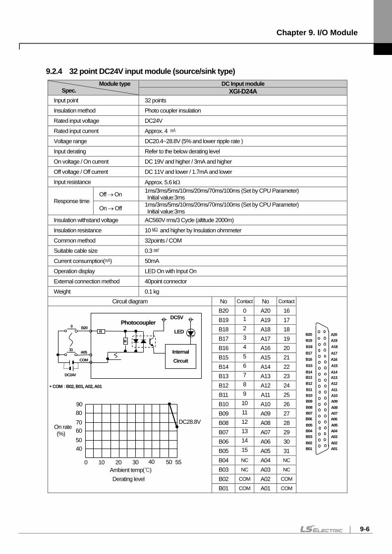
Chapter 9. I/O Module
9-6
9.2.4 32 point DC24V input module (source/sink type) Module type
Spec. DC Input module
XGI-D24A Input point 32 points
Insulation method Photo coupler insulation
Rated input voltage DC24V
Rated input current Approx. 4
Voltage range DC20.4~28.8V (5% and lower ripple rate )
Input derating Refer to the below derating level
On voltage / On current DC 19V and higher / 3mA and higher
Off voltage / Off current DC 11V and lower / 1.7mA and lower
Input resistance Approx. 5.6 kΩ
Response time Off → On 1ms/3ms/5ms/10ms/20ms/70ms/100ms (Set by CPU Parameter)
Initial value:3ms
On → Off 1ms/3ms/5ms/10ms/20ms/70ms/100ms (Set by CPU Parameter) Initial value:3ms
Insulation withstand voltage AC560V rms/3 Cycle (altitude 2000m)
Insulation resistance 10 and higher by Insulation ohmmeter
Common method 32points / COM
Suitable cable size 0.3
Current consumption() 50mA
Operation display LED On with Input On
External connection method 40point connector
Weight 0.1 kg Circuit diagram No Contact No Contact
B20 0 A20 16 B19 1 A19 17 B18 2 A18 18 B17 3 A17 19 B16 4 A16 20 B15 5 A15 21 B14 6 A14 22 B13 7 A13 23 B12 8 A12 24 B11 9 A11 25 B10 10 A10 26 B09 11 A09 27 B08 12 A08 28 B07 13 A07 29 B06 14 A06 30 B05 15 A05 31 B04 NC A04 NC
B03 NC A03 NC B02 COM A02 COM B01 COM A01 COM
B20 B19 B18 B17 B16 B15 B14 B13 B12 B11 B10 B09 B08 B07 B06 B05 B04 B03 B02 B01
A20 A19 A18 A17 A16 A15 A14 A13 A12 A11 A10 A09 A08 A07 A06 A05 A04 A03 A02 A01
DC28.8V 80
60
40
0 10 20 30 40 50 55
On rate (%)
Ambient temp() Derating level
90
70
50
DC24V
Internal Circuit
R
0
B20
COM
Photocoupler
* COM : B02, B01, A02, A01
A05
R
31
DC5V
LED
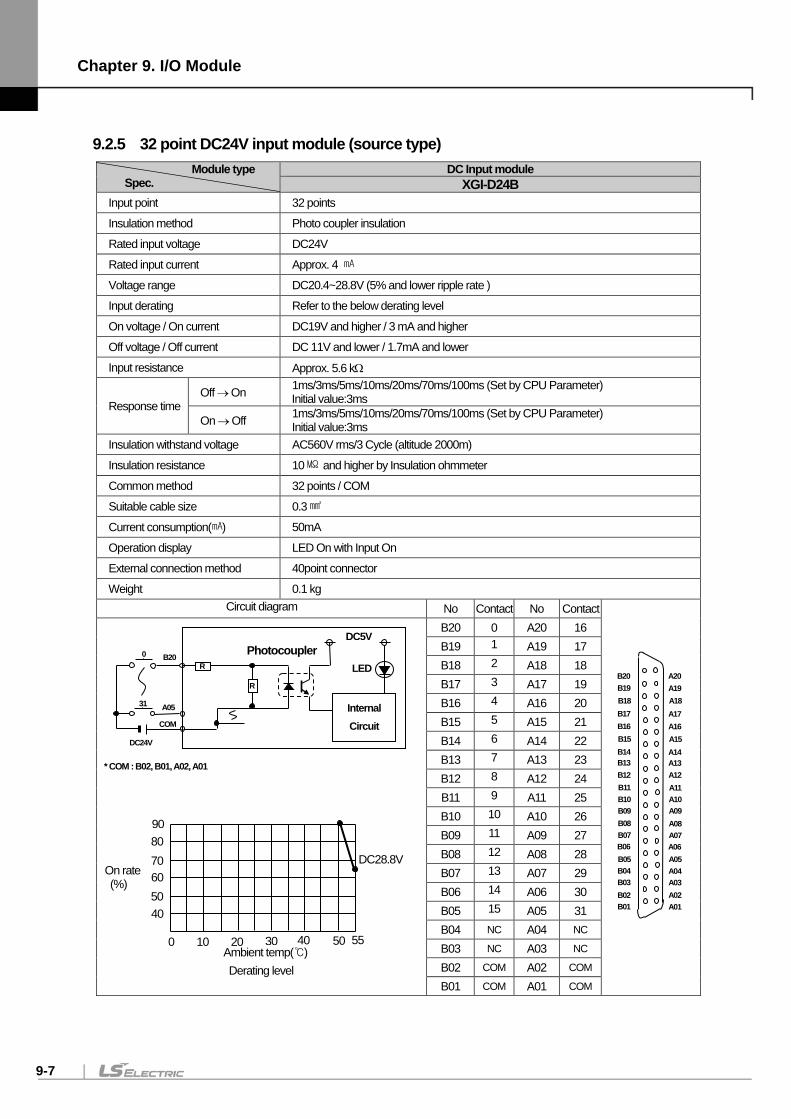
Chapter 9. I/O Module
9-7
9.2.5 32 point DC24V input module (source type) Module type
Spec. DC Input module
XGI-D24B Input point 32 points
Insulation method Photo coupler insulation
Rated input voltage DC24V
Rated input current Approx. 4
Voltage range DC20.4~28.8V (5% and lower ripple rate )
Input derating Refer to the below derating level
On voltage / On current DC19V and higher / 3 mA and higher
Off voltage / Off current DC 11V and lower / 1.7mA and lower
Input resistance Approx. 5.6 kΩ
Response time Off → On 1ms/3ms/5ms/10ms/20ms/70ms/100ms (Set by CPU Parameter)
Initial value:3ms
On → Off 1ms/3ms/5ms/10ms/20ms/70ms/100ms (Set by CPU Parameter) Initial value:3ms
Insulation withstand voltage AC560V rms/3 Cycle (altitude 2000m)
Insulation resistance 10 and higher by Insulation ohmmeter
Common method 32 points / COM
Suitable cable size 0.3
Current consumption() 50mA
Operation display LED On with Input On
External connection method 40point connector
Weight 0.1 kg Circuit diagram No Contact No Contact
B20 0 A20 16 B19 1 A19 17 B18 2 A18 18 B17 3 A17 19 B16 4 A16 20 B15 5 A15 21 B14 6 A14 22 B13 7 A13 23 B12 8 A12 24 B11 9 A11 25 B10 10 A10 26 B09 11 A09 27 B08 12 A08 28 B07 13 A07 29 B06 14 A06 30 B05 15 A05 31 B04 NC A04 NC
B03 NC A03 NC B02 COM A02 COM B01 COM A01 COM
B20 B19 B18 B17 B16 B15 B14 B13 B12 B11 B10 B09 B08 B07 B06 B05 B04 B03 B02 B01
A20 A19 A18 A17 A16 A15 A14 A13 A12 A11 A10 A09 A08 A07 A06 A05 A04 A03 A02 A01
DC28.8V 80
60
40
0 10 20 30 40 50 55
On rate (%)
Ambient temp() Derating level
90
70
50
* COM : B02, B01, A02, A01
DC24V
R
31
0
B20
COM
A05
R
Photocoupler
Internal Circuit
DC5V
LED
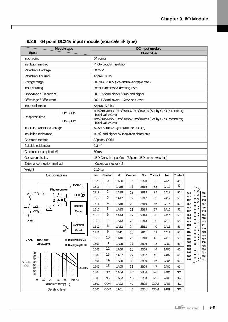
Chapter 9. I/O Module
9-8
9.2.6 64 point DC24V input module (source/sink type) Module type
Spec. DC Input module
XGI-D28A Input point 64 points
Insulation method Photo coupler insulation
Rated input voltage DC24V
Rated input current Approx. 4
Voltage range DC20.4~28.8V (5% and lower ripple rate )
Input derating Refer to the below derating level
On voltage / On current DC 19V and higher / 3mA and higher
Off voltage / Off current DC 11V and lower / 1.7mA and lower
Input resistance Approx. 5.6 kΩ
Response time Off → On 1ms/3ms/5ms/10ms/20ms/70ms/100ms (Set by CPU Parameter)
Initial value:3ms
On → Off 1ms/3ms/5ms/10ms/20ms/70ms/100ms (Set by CPU Parameter) Initial value:3ms
Insulation withstand voltage AC560V rms/3 Cycle (altitude 2000m)
Insulation resistance 10 and higher by Insulation ohmmeter
Common method 32point / COM
Suitable cable size 0.3
Current consumption() 60mA
Operation display LED On with Input On (32point LED on by switching)
External connection method 40point connector × 2
Weight 0.15 kg Circuit diagram No Contact No Contact No Contact No Contact
1B20 0 1A20 16 2B20 32 2A20 48
1B19 1 1A19 17 2B19 33 2A19 49
1B18 2 1A18 18 2B18 34 2A18 50
1B17 3 1A17 19 2B17 35 2A17 51
1B16 4 1A16 20 2B16 36 2A16 52
1B15 5 1A15 21 2B15 37 2A15 53
1B14 6 1A14 22 2B14 38 2A14 54
1B13 7 1A13 23 2B13 39 2A13 55
1B12 8 1A12 24 2B12 40 2A12 56
1B11 9 1A11 25 2B11 41 2A11 57
1B10 10 1A10 26 2B10 42 2A10 58
1B09 11 1A09 27 2B09 43 2A09 59
1B08 12 1A08 28 2B08 44 2A08 60
1B07 13 1A07 29 2B07 45 2A07 61
1B06 14 1A06 30 2B06 46 2A06 62
1B05 15 1A05 31 2B05 47 2A05 63
1B04 NC 1A04 NC 2B04 NC 2A04 NC
1B03 NC 1A03 NC 2B03 NC 2A03 NC
1B02 COM 1A02 NC 2B02 COM 2A02 NC
1B01 COM 1A01 NC 2B01 COM 2A01 NC
B20 B19 B18 B17 B16 B15 B14 B13 B12 B11 B10 B09 B08 B07 B06 B05 B04 B03 B02 B01
A20 A19 A18 A17 A16 A15 A14 A13 A12 A11 A10 A09 A08 A07 A06 A05 A04 A03 A02 A01
DC28.8V
20 30 40 50 60 70
80 90
0 10 20 30 40 50 55
On rate (%)
Ambient temp() Derating level
Internal
Circuit
DC24V
R
63
0
1B20
* COM : 1B02, 1B01 2B02, 2B01
2A05
R
Switching
Circuit
A
B
A: Displaying 0~31
B: Displaying 32~63
COM
Photocoupler DC5V
LED
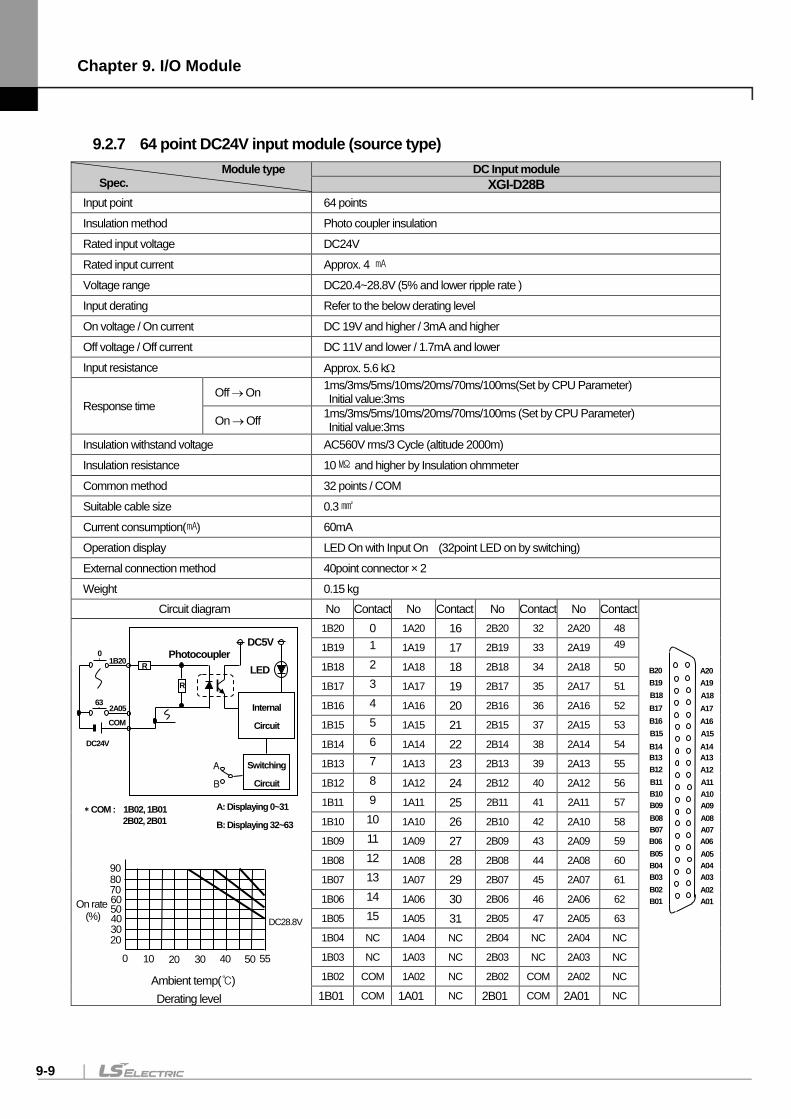
Chapter 9. I/O Module
9-9
9.2.7 64 point DC24V input module (source type) Module type
Spec. DC Input module
XGI-D28B Input point 64 points
Insulation method Photo coupler insulation
Rated input voltage DC24V
Rated input current Approx. 4
Voltage range DC20.4~28.8V (5% and lower ripple rate )
Input derating Refer to the below derating level
On voltage / On current DC 19V and higher / 3mA and higher
Off voltage / Off current DC 11V and lower / 1.7mA and lower
Input resistance Approx. 5.6 kΩ
Response time Off → On 1ms/3ms/5ms/10ms/20ms/70ms/100ms(Set by CPU Parameter)
Initial value:3ms
On → Off 1ms/3ms/5ms/10ms/20ms/70ms/100ms (Set by CPU Parameter) Initial value:3ms
Insulation withstand voltage AC560V rms/3 Cycle (altitude 2000m)
Insulation resistance 10 and higher by Insulation ohmmeter
Common method 32 points / COM
Suitable cable size 0.3
Current consumption() 60mA
Operation display LED On with Input On (32point LED on by switching)
External connection method 40point connector × 2
Weight 0.15 kg Circuit diagram No Contact No Contact No Contact No Contact
1B20 0 1A20 16 2B20 32 2A20 48
1B19 1 1A19 17 2B19 33 2A19 49
1B18 2 1A18 18 2B18 34 2A18 50
1B17 3 1A17 19 2B17 35 2A17 51
1B16 4 1A16 20 2B16 36 2A16 52
1B15 5 1A15 21 2B15 37 2A15 53
1B14 6 1A14 22 2B14 38 2A14 54
1B13 7 1A13 23 2B13 39 2A13 55
1B12 8 1A12 24 2B12 40 2A12 56
1B11 9 1A11 25 2B11 41 2A11 57
1B10 10 1A10 26 2B10 42 2A10 58
1B09 11 1A09 27 2B09 43 2A09 59
1B08 12 1A08 28 2B08 44 2A08 60
1B07 13 1A07 29 2B07 45 2A07 61
1B06 14 1A06 30 2B06 46 2A06 62
1B05 15 1A05 31 2B05 47 2A05 63
1B04 NC 1A04 NC 2B04 NC 2A04 NC
1B03 NC 1A03 NC 2B03 NC 2A03 NC
1B02 COM 1A02 NC 2B02 COM 2A02 NC
1B01 COM 1A01 NC 2B01 COM 2A01 NC
B20 B19 B18 B17 B16 B15 B14 B13 B12 B11 B10 B09 B08 B07 B06 B05 B04 B03 B02 B01
A20 A19 A18 A17 A16 A15 A14 A13 A12 A11 A10 A09 A08 A07 A06 A05 A04 A03 A02 A01
DC28.8V
20 30 40 50 60 70 80 90
0 10 20 30 40 50 55
Ambient temp() Derating level
On rate (%)
DC24V
R
63
0
COM
* COM : 1B02, 1B01 /2B02, 2B01
2A05
R
A
B
1B20
A: Displaying 0~31
B: Displaying 32~63
Switching
Circuit
Internal
Circuit
Photocoupler DC5V
LED
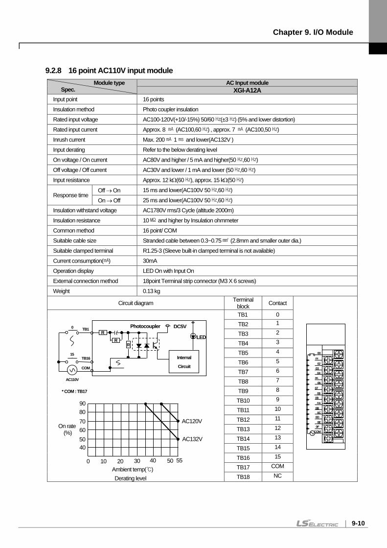
Chapter 9. I/O Module
9-10
9.2.8 16 point AC110V input module Module type
Spec. AC Input module
XGI-A12A Input point 16 points
Insulation method Photo coupler insulation
Rated input voltage AC100-120V(+10/-15%) 50/60(±3) (5% and lower distortion)
Rated input current Approx. 8 (AC100,60) , approx. 7 (AC100,50)
Inrush current Max. 200 1 and lower(AC132V )
Input derating Refer to the below derating level
On voltage / On current AC80V and higher / 5 mA and higher(50,60)
Off voltage / Off current AC30V and lower / 1 mA and lower (50,60)
Input resistance Approx. 12 kΩ(60), approx. 15 kΩ(50)
Response time Off → On 15 ms and lower(AC100V 50,60)
On → Off 25 ms and lower(AC100V 50,60)
Insulation withstand voltage AC1780V rms/3 Cycle (altitude 2000m)
Insulation resistance 10 and higher by Insulation ohmmeter
Common method 16 point/ COM
Suitable cable size Stranded cable between 0.3~0.75 (2.8mm and smaller outer dia.)
Suitable clamped terminal R1.25-3 (Sleeve built-in clamped terminal is not available)
Current consumption() 30mA
Operation display LED On with Input On
External connection method 18point Terminal strip connector (M3 X 6 screws)
Weight 0.13 kg
Circuit diagram Terminal block Contact
TB1 0 TB2 1
TB3 2
TB4 3
TB5 4
TB6 5
TB7 6
TB8 7
TB9 8
TB10 9
TB11 10
TB12 11
TB13 12
TB14 13
TB15 14
TB16 15
TB17 COM
TB18 NC
00
06
0D
COM
01 02
03 04
05
0A 0B
0C
0F 0E
08 07
09
AC120V 80
60
40
0 10 20 30 40 50 55
90
70
50 AC132V
On rate (%)
Ambient temp() Derating level
* COM : TB17
AC110V
R
15
0
TB1
COM
R
TB16
R
DC5V
LED
Photocoupler
Internal
Circuit
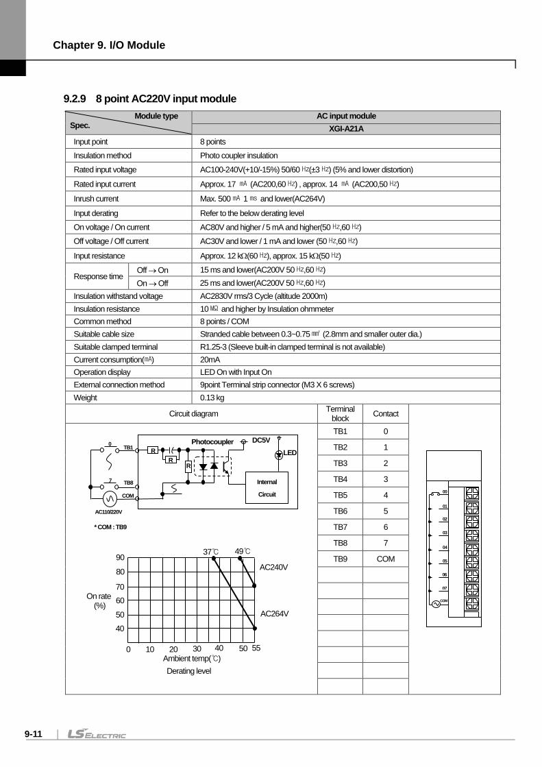
Chapter 9. I/O Module
9-11
9.2.9 8 point AC220V input module Module type
Spec. AC input module
XGI-A21A Input point 8 points Insulation method Photo coupler insulation
Rated input voltage AC100-240V(+10/-15%) 50/60(±3) (5% and lower distortion)
Rated input current Approx. 17 (AC200,60) , approx. 14 (AC200,50)
Inrush current Max. 500 1 and lower(AC264V)
Input derating Refer to the below derating level On voltage / On current AC80V and higher / 5 mA and higher(50,60) Off voltage / Off current AC30V and lower / 1 mA and lower (50,60)
Input resistance Approx. 12 kΩ(60), approx. 15 kΩ(50)
Response time Off → On 15 ms and lower(AC200V 50,60) On → Off 25 ms and lower(AC200V 50,60)
Insulation withstand voltage AC2830V rms/3 Cycle (altitude 2000m) Insulation resistance 10 and higher by Insulation ohmmeter Common method 8 points / COM Suitable cable size Stranded cable between 0.3~0.75 (2.8mm and smaller outer dia.) Suitable clamped terminal R1.25-3 (Sleeve built-in clamped terminal is not available) Current consumption() 20mA Operation display LED On with Input On External connection method 9point Terminal strip connector (M3 X 6 screws) Weight 0.13 kg
Circuit diagram Terminal block Contact
TB1 0
TB2 1
TB3 2
TB4 3
TB5 4
TB6 5
TB7 6
TB8 7
TB9 COM
DC5V
AC110/220V
R
7
0
TB1
COM
R
* COM : TB9
R
TB8
LED
AC240V 80
60
40
0 10 20 30 40 50 55
90
70
50 AC264V
37 49
On rate (%)
Ambient temp() Derating level
Photocoupler
Internal
Circuit
00
COM
01
02
03
04
05
06
07
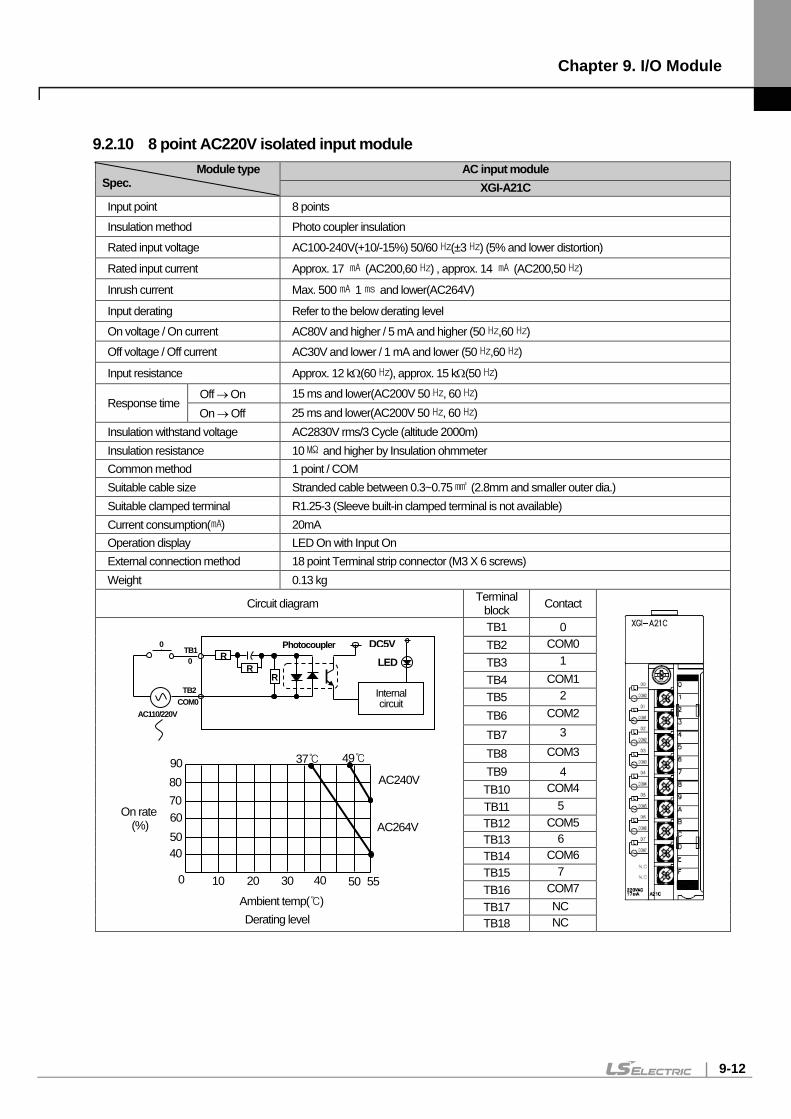
Chapter 9. I/O Module
9-12
9.2.10 8 point AC220V isolated input module Module type
Spec. AC input module
XGI-A21C Input point 8 points Insulation method Photo coupler insulation
Rated input voltage AC100-240V(+10/-15%) 50/60(±3) (5% and lower distortion)
Rated input current Approx. 17 (AC200,60) , approx. 14 (AC200,50)
Inrush current Max. 500 1 and lower(AC264V)
Input derating Refer to the below derating level On voltage / On current AC80V and higher / 5 mA and higher (50,60) Off voltage / Off current AC30V and lower / 1 mA and lower (50,60)
Input resistance Approx. 12 kΩ(60), approx. 15 kΩ(50)
Response time Off → On 15 ms and lower(AC200V 50, 60) On → Off 25 ms and lower(AC200V 50, 60)
Insulation withstand voltage AC2830V rms/3 Cycle (altitude 2000m) Insulation resistance 10 and higher by Insulation ohmmeter Common method 1 point / COM Suitable cable size Stranded cable between 0.3~0.75 (2.8mm and smaller outer dia.) Suitable clamped terminal R1.25-3 (Sleeve built-in clamped terminal is not available) Current consumption() 20mA Operation display LED On with Input On External connection method 18 point Terminal strip connector (M3 X 6 screws) Weight 0.13 kg
Circuit diagram Terminal block Contact
TB1 0 TB2 COM0 TB3 1 TB4 COM1 TB5 2 TB6 COM2
TB7 3
TB8 COM3 TB9 4 TB10 COM4 TB11 5 TB12 COM5 TB13 6 TB14 COM6 TB15 7 TB16 COM7 TB17 NC TB18 NC
Internal circuit
R Photocoupler
R
0
TB1
TB2
AC110/220V
DC5V LED
COM0
0
R
AC240V 80
60
40
0 10 20 30 40 50 55
90
70
50 AC264V
37 49
Ambient temp() Derating level
On rate (%)
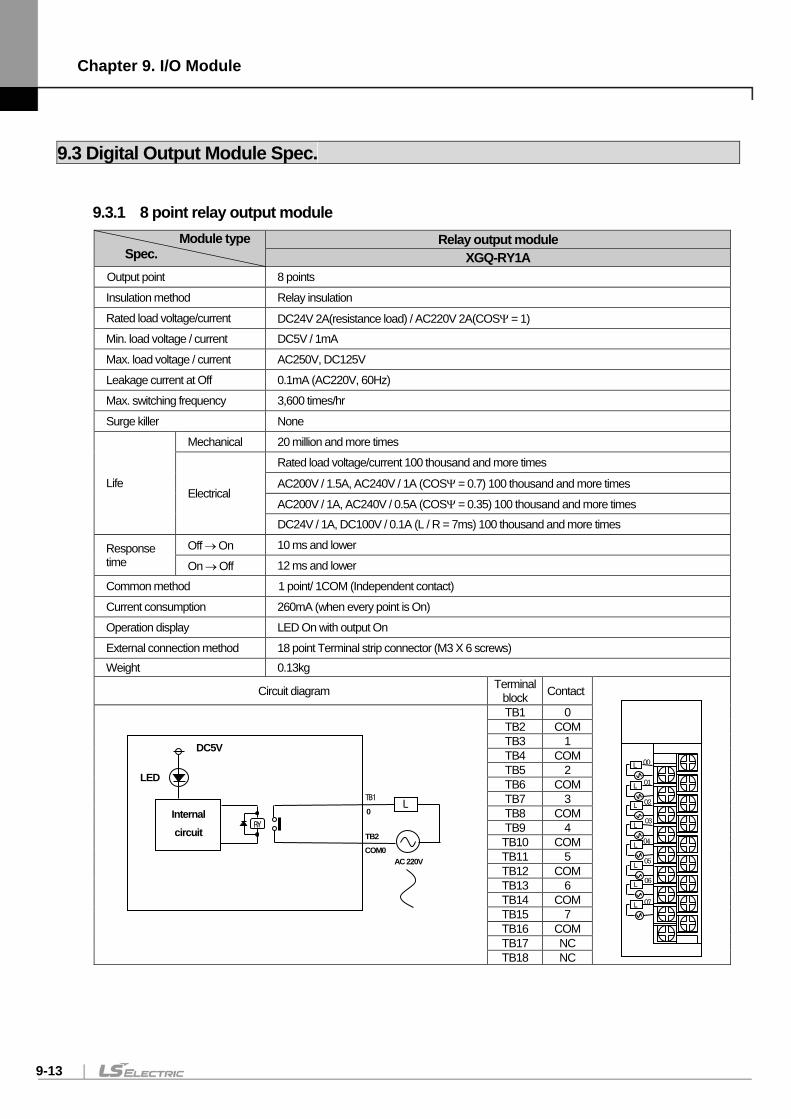
Chapter 9. I/O Module
9-13
9.3 Digital Output Module Spec.
9.3.1 8 point relay output module Module type Spec.
Relay output module XGQ-RY1A
Output point 8 points
Insulation method Relay insulation
Rated load voltage/current DC24V 2A(resistance load) / AC220V 2A(COSΨ = 1) Min. load voltage / current DC5V / 1mA
Max. load voltage / current AC250V, DC125V
Leakage current at Off 0.1mA (AC220V, 60Hz)
Max. switching frequency 3,600 times/hr
Surge killer None
Life
Mechanical 20 million and more times
Electrical
Rated load voltage/current 100 thousand and more times
AC200V / 1.5A, AC240V / 1A (COSΨ = 0.7) 100 thousand and more times
AC200V / 1A, AC240V / 0.5A (COSΨ = 0.35) 100 thousand and more times DC24V / 1A, DC100V / 0.1A (L / R = 7ms) 100 thousand and more times
Response time
Off → On 10 ms and lower
On → Off 12 ms and lower
Common method 1 point/ 1COM (Independent contact)
Current consumption 260mA (when every point is On)
Operation display LED On with output On
External connection method 18 point Terminal strip connector (M3 X 6 screws) Weight 0.13kg
Circuit diagram Terminal block Contact
TB1 0 TB2 COM TB3 1 TB4 COM TB5 2 TB6 COM TB7 3 TB8 COM TB9 4 TB10 COM TB11 5 TB12 COM TB13 6 TB14 COM TB15 7 TB16 COM TB17 NC TB18 NC
00
05
07
01
02
03
04
06
L L L L L L L L
RY Internal circuit
TB1
TB2
L
LED
DC5V
AC 220V
0
COM0
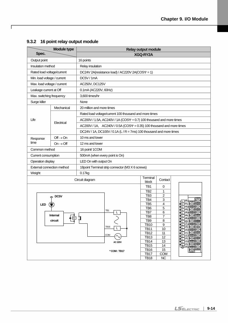
Chapter 9. I/O Module
9-14
9.3.2 16 point relay output module Module type
Spec. Relay output module
XGQ-RY2A Output point 16 points
Insulation method Relay insulation
Rated load voltage/current DC24V 2A(resistance load) / AC220V 2A(COSΨ = 1) Min. load voltage / current DC5V / 1mA
Max. load voltage / current AC250V, DC125V
Leakage current at Off 0.1mA (AC220V, 60Hz)
Max. switching frequency 3,600 times/hr
Surge killer None
Life
Mechanical 20 million and more times
Electrical
Rated load voltage/current 100 thousand and more times
AC200V / 1.5A, AC240V / 1A (COSΨ = 0.7) 100 thousand and more times
AC200V / 1A, AC240V / 0.5A (COSΨ = 0.35) 100 thousand and more times DC24V / 1A, DC100V / 0.1A (L / R = 7ms) 100 thousand and more times
Response time
Off → On 10 ms and lower
On → Off 12 ms and lower
Common method 16 point/ 1COM
Current consumption 500mA (when every point is On)
Operation display LED On with output On
External connection method 18point Terminal strip connector (M3 X 6 screws) Weight 0.17kg
Circuit diagram Terminal block Contact
TB1 0 TB2 1 TB3 2 TB4 3 TB5 4 TB6 5 TB7 6 TB8 7 TB9 8 TB10 9 TB11 10 TB12 11 TB13 12 TB14 13 TB15 14 TB16 15 TB17 COM TB18 NC
00
10
14
02.
04
06
08
12
L L L L L L L L L L L L L L L
L
01.
03.
05
07
09
11
13
15
COM
RY Internal circuit
TB1
TB16
L
L
DC5V
LED
AC 220V
* COM : TB17
COM
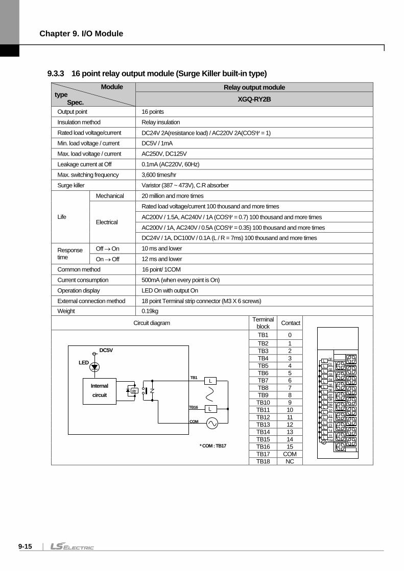
Chapter 9. I/O Module
9-15
9.3.3 16 point relay output module (Surge Killer built-in type) Module
type Spec.
Relay output module XGQ-RY2B
Output point 16 points
Insulation method Relay insulation
Rated load voltage/current DC24V 2A(resistance load) / AC220V 2A(COSΨ = 1) Min. load voltage / current DC5V / 1mA
Max. load voltage / current AC250V, DC125V
Leakage current at Off 0.1mA (AC220V, 60Hz)
Max. switching frequency 3,600 times/hr
Surge killer Varistor (387 ~ 473V), C.R absorber
Life
Mechanical 20 million and more times
Electrical
Rated load voltage/current 100 thousand and more times
AC200V / 1.5A, AC240V / 1A (COSΨ = 0.7) 100 thousand and more times
AC200V / 1A, AC240V / 0.5A (COSΨ = 0.35) 100 thousand and more times DC24V / 1A, DC100V / 0.1A (L / R = 7ms) 100 thousand and more times
Response time
Off → On 10 ms and lower
On → Off 12 ms and lower
Common method 16 point/ 1COM
Current consumption 500mA (when every point is On)
Operation display LED On with output On
External connection method 18 point Terminal strip connector (M3 X 6 screws) Weight 0.19kg
Circuit diagram Terminal block Contact
TB1 0 TB2 1 TB3 2 TB4 3 TB5 4 TB6 5 TB7 6 TB8 7 TB9 8 TB10 9 TB11 10 TB12 11 TB13 12 TB14 13 TB15 14 TB16 15 TB17 COM TB18 NC
00
10
14
02.
04
06
08
12
L L L L L L L L L L L L L L L
L
01
03.
05
07
09
11
13
15
COM
RY
Internal circuit
TB1
COM
TB16
L
L
LED
DC5V
* COM : TB17
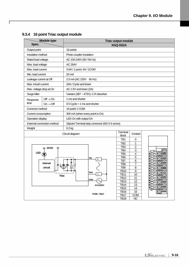
Chapter 9. I/O Module
9-16
9.3.4 16 point Triac output module Module type
Spec. Triac output module
XGQ-SS2A Output point 16 points
Insulation method Photo coupler insulation
Rated load voltage AC 100-240V (50 / 60 Hz)
Max. load voltage AC 264V
Max. load current 0.6A / 1 point, 4A / 1COM
Min. load current 20 mA
Leakage current at Off 2.5 mA (AC 220V 60 Hz)
Max. inrush current 20A / Cycle and lower
Max. voltage drop at On AC 1.5V and lower (2A)
Surge killer Varistor (387 ~ 473V), C.R absorber
Response time
Off → On 1 ms and shorter
On → Off 0.5 Cycle + 1 ms and shorter
Common method 16 point/ 1 COM
Current consumption 300 mA (when every point is On)
Operation display LED On with output On
External connection method 18point Terminal strip connector (M3 X 6 screw) Weight 0.2 kg
Circuit diagram Terminal block Contact
TB1 0 TB2 1 TB3 2 TB4 3 TB5 4 TB6 5 TB7 6 TB8 7 TB9 8 TB10 9 TB11 10 TB12 11 TB13 12 TB14 13 TB15 14 TB16 15 TB17 COM TB18 NC
00
10
14
02.
04
06
08
12
L L L L L L L L L L L L L L L
L
01.
03.
05
07
09
11
13
15
COM
DC5V
R
Internal circuit
TB1
COM
TB16
ZC
Triac L
L
LED
*COM : TB17
AC110/220V
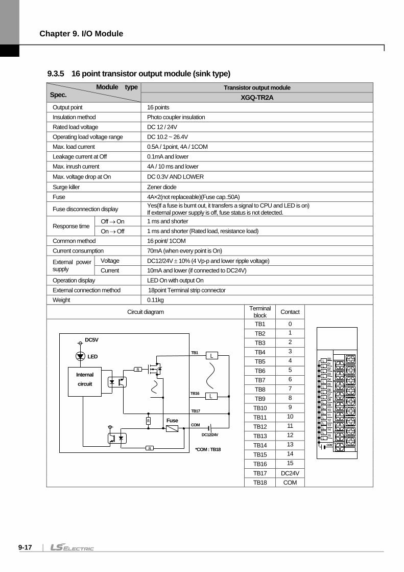
Chapter 9. I/O Module
9-17
9.3.5 16 point transistor output module (sink type) Module type Spec.
Transistor output module XGQ-TR2A
Output point 16 points Insulation method Photo coupler insulation Rated load voltage DC 12 / 24V Operating load voltage range DC 10.2 ~ 26.4V Max. load current 0.5A / 1point, 4A / 1COM Leakage current at Off 0.1mA and lower Max. inrush current 4A / 10 ms and lower Max. voltage drop at On DC 0.3V AND LOWER Surge killer Zener diode Fuse 4A×2(not replaceable)(Fuse cap.:50A)
Fuse disconnection display Yes(If a fuse is burnt out, it transfers a signal to CPU and LED is on) If external power supply is off, fuse status is not detected.
Response time Off → On 1 ms and shorter On → Off 1 ms and shorter (Rated load, resistance load)
Common method 16 point/ 1COM Current consumption 70mA (when every point is On)
External power supply
Voltage DC12/24V ± 10% (4 Vp-p and lower ripple voltage) Current 10mA and lower (if connected to DC24V)
Operation display LED On with output On External connection method 18point Terminal strip connector Weight 0.11kg
Circuit diagram Terminal block Contact
TB1 0 TB2 1 TB3 2 TB4 3 TB5 4 TB6 5 TB7 6 TB8 7 TB9 8 TB10 9 TB11 10 TB12 11 TB13 12 TB14 13 TB15 14 TB16 15 TB17 DC24V TB18 COM
DC12/24V
R
Internal circuit
TB1
TB17
TB16
Fuse COM
R
R
L
L
LED
*COM : TB18
DC5V
L L L L L L L L L L L L L L L
L
00
01
02
03
04
05
06
07
08
09
10
11
12
13
14
15
COM
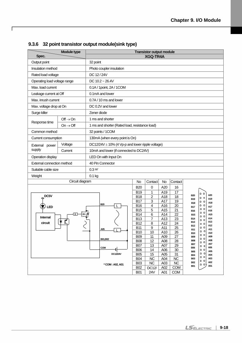
Chapter 9. I/O Module
9-18
9.3.6 32 point transistor output module(sink type) Module type
Spec. Transistor output module
XGQ-TR4A Output point 32 point
Insulation method Photo coupler insulation
Rated load voltage DC 12 / 24V
Operating load voltage range DC 10.2 ~ 26.4V
Max. load current 0.1A / 1point, 2A / 1COM
Leakage current at Off 0.1mA and lower
Max. inrush current 0.7A / 10 ms and lower
Max. voltage drop at On DC 0.2V and lower
Surge killer Zener diode
Response time Off → On 1 ms and shorter
On → Off 1 ms and shorter (Rated load, resistance load)
Common method 32 points / 1COM
Current consumption 130mA (when every point is On)
External power supply
Voltage DC12/24V ± 10% (4 Vp-p and lower ripple voltage) Current 10mA and lower (if connected to DC24V)
Operation display LED On with Input On
External connection method 40 Pin Connector
Suitable cable size 0.3
Weight 0.1 kg Circuit diagram No Contact No Contact
B20 0 A20 16 B19 1 A19 17 B18 2 A18 18 B17 3 A17 19 B16 4 A16 20 B15 5 A15 21 B14 6 A14 22 B13 7 A13 23 B12 8 A12 24 B11 9 A11 25 B10 10 A10 26 B09 11 A09 27 B08 12 A08 28 B07 13 A07 29 B06 14 A06 30 B05 15 A05 31 B04 /NC A04 NC B03 NC A03 NC B02 DC12/
24V A02 COM
B01 A01 COM
B20 B19 B18 B17 B16 B15 B14 B13 B12 B11 B10 B09 B08 B07 B06 B05 B04 B03 B02 B01
A20 A19 A18 A17 A16 A15 A14 A13 A12 A11 A10 A09 A08 A07 A06 A05 A04 A03 A02 A01
DC12/24V
R
Internal circuit
B20
B01,B02
A05
COM
L
L
LED
* COM : A02, A01
DC5V
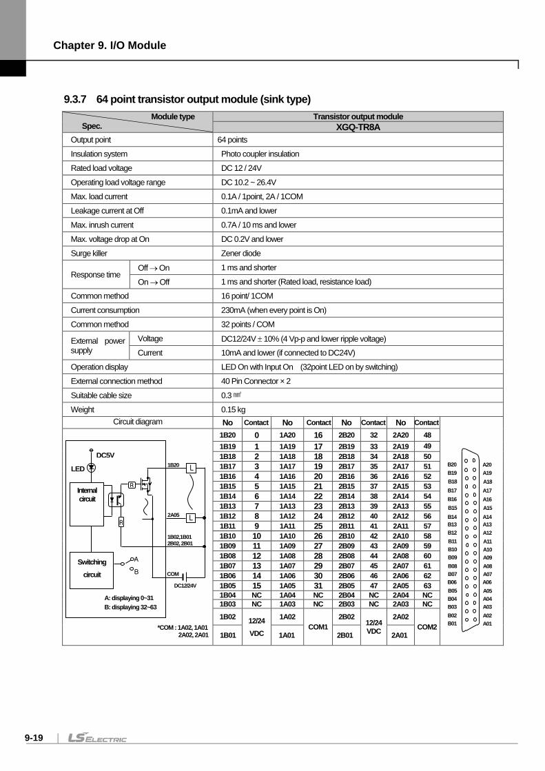
Chapter 9. I/O Module
9-19
9.3.7 64 point transistor output module (sink type) Module type
Spec. Transistor output module
XGQ-TR8A Output point 64 points
Insulation system Photo coupler insulation
Rated load voltage DC 12 / 24V
Operating load voltage range DC 10.2 ~ 26.4V
Max. load current 0.1A / 1point, 2A / 1COM
Leakage current at Off 0.1mA and lower
Max. inrush current 0.7A / 10 ms and lower
Max. voltage drop at On DC 0.2V and lower
Surge killer Zener diode
Response time Off → On 1 ms and shorter
On → Off 1 ms and shorter (Rated load, resistance load)
Common method 16 point/ 1COM
Current consumption 230mA (when every point is On)
Common method 32 points / COM
External power supply
Voltage DC12/24V ± 10% (4 Vp-p and lower ripple voltage) Current 10mA and lower (if connected to DC24V)
Operation display LED On with Input On (32point LED on by switching)
External connection method 40 Pin Connector × 2
Suitable cable size 0.3
Weight 0.15 kg Circuit diagram No Contact No Contact No Contact No Contact
1B20 0 1A20 16 2B20 32 2A20 48 1B19 1 1A19 17 2B19 33 2A19 49 1B18 2 1A18 18 2B18 34 2A18 50 1B17 3 1A17 19 2B17 35 2A17 51 1B16 4 1A16 20 2B16 36 2A16 52 1B15 5 1A15 21 2B15 37 2A15 53 1B14 6 1A14 22 2B14 38 2A14 54 1B13 7 1A13 23 2B13 39 2A13 55 1B12 8 1A12 24 2B12 40 2A12 56 1B11 9 1A11 25 2B11 41 2A11 57 1B10 10 1A10 26 2B10 42 2A10 58 1B09 11 1A09 27 2B09 43 2A09 59 1B08 12 1A08 28 2B08 44 2A08 60 1B07 13 1A07 29 2B07 45 2A07 61 1B06 14 1A06 30 2B06 46 2A06 62 1B05 15 1A05 31 2B05 47 2A05 63 1B04 NC 1A04 NC 2B04 NC 2A04 NC 1B03 NC 1A03 NC 2B03 NC 2A03 NC 1B02 12/24
VDC
1A02 COM1
2B02 12/24VDC
2A02 COM2
*1B01 1A01 2B01 2A01
B20 B19 B18 B17 B16 B15 B14 B13 B12 B11 B10 B09 B08 B07 B06 B05 B04 B03 B02 B01
A20 A19 A18 A17 A16 A15 A14 A13 A12 A11 A10 A09 A08 A07 A06 A05 A04 A03 A02 A01
R
*COM : 1A02, 1A01 / 2A02, 2A01
DC12/24V
Internal circuit
L LED
1B20
1B02,1B01 2B02, 2B01
L
2A05
COM
R
Switching circuit
A
B
A: displaying 0~31 B: displaying 32~63
DC5V
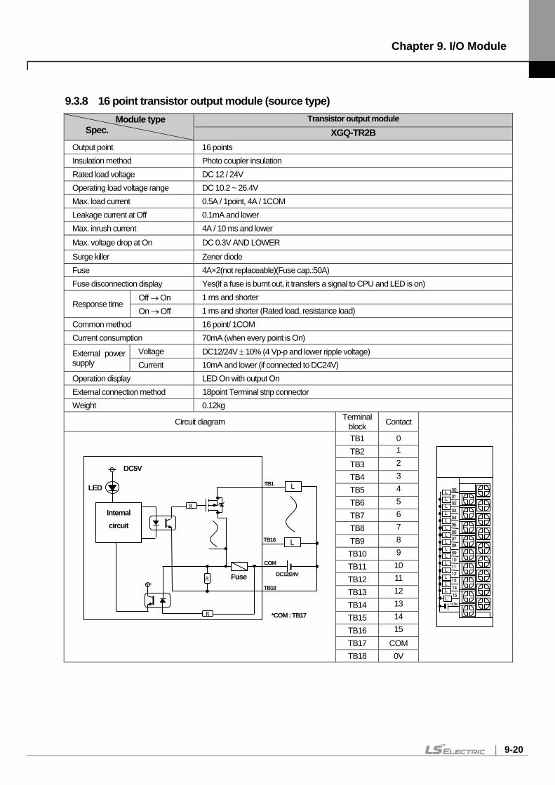
Chapter 9. I/O Module
9-20
9.3.8 16 point transistor output module (source type) Module type
Spec. Transistor output module
XGQ-TR2B Output point 16 points Insulation method Photo coupler insulation Rated load voltage DC 12 / 24V Operating load voltage range DC 10.2 ~ 26.4V Max. load current 0.5A / 1point, 4A / 1COM Leakage current at Off 0.1mA and lower Max. inrush current 4A / 10 ms and lower Max. voltage drop at On DC 0.3V AND LOWER Surge killer Zener diode Fuse 4A×2(not replaceable)(Fuse cap.:50A) Fuse disconnection display Yes(If a fuse is burnt out, it transfers a signal to CPU and LED is on)
Response time Off → On 1 ms and shorter On → Off 1 ms and shorter (Rated load, resistance load)
Common method 16 point/ 1COM Current consumption 70mA (when every point is On)
External power supply
Voltage DC12/24V ± 10% (4 Vp-p and lower ripple voltage) Current 10mA and lower (if connected to DC24V)
Operation display LED On with output On External connection method 18point Terminal strip connector Weight 0.12kg
Circuit diagram Terminal block Contact
TB1 0 TB2 1 TB3 2 TB4 3 TB5 4 TB6 5 TB7 6 TB8 7 TB9 8 TB10 9 TB11 10 TB12 11 TB13 12 TB14 13 TB15 14 TB16 15 TB17 COM TB18 0V
*COM : TB17
DC12/24V
R
Internal circuit
L LED
TB1
COM
TB16
Fuse TB18
R
R
L
DC5V
L L L L L L L L L L L
L L L
L
00
01
02
03
04
05
06
07
08
09
10
11
12
13
14
15
COM
L
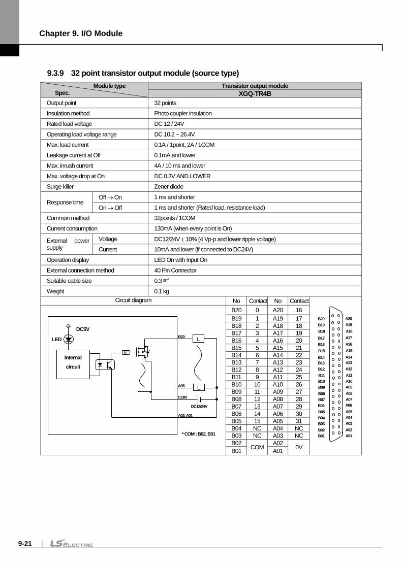
Chapter 9. I/O Module
9-21
9.3.9 32 point transistor output module (source type) Module type
Spec. Transistor output module
XGQ-TR4B Output point 32 points
Insulation method Photo coupler insulation
Rated load voltage DC 12 / 24V
Operating load voltage range DC 10.2 ~ 26.4V
Max. load current 0.1A / 1point, 2A / 1COM
Leakage current at Off 0.1mA and lower
Max. inrush current 4A / 10 ms and lower
Max. voltage drop at On DC 0.3V AND LOWER
Surge killer Zener diode
Response time Off → On 1 ms and shorter
On → Off 1 ms and shorter (Rated load, resistance load)
Common method 32points / 1COM
Current consumption 130mA (when every point is On)
External power supply
Voltage DC12/24V ± 10% (4 Vp-p and lower ripple voltage) Current 10mA and lower (if connected to DC24V)
Operation display LED On with Input On
External connection method 40 Pin Connector
Suitable cable size 0.3
Weight 0.1 kg Circuit diagram No Contact No Contact
B20 0 A20 16 B19 1 A19 17 B18 2 A18 18 B17 3 A17 19 B16 4 A16 20 B15 5 A15 21 B14 6 A14 22 B13 7 A13 23 B12 8 A12 24 B11 9 A11 25 B10 10 A10 26 B09 11 A09 27 B08 12 A08 28 B07 13 A07 29 B06 14 A06 30 B05 15 A05 31 B04 NC A04 NC B03 NC A03 NC B02
COM A02
0V B01 A01
B20 B19 B18 B17 B16 B15 B14 B13 B12 B11 B10 B09 B08 B07 B06 B05 B04 B03 B02 B01
A20 A19 A18 A17 A16 A15 A14 A13 A12 A11 A10 A09 A08 A07 A06 A05 A04 A03 A02 A01
DC12/24V
* COM : B02, B01
R
Internal circuit
LED
B20
COM
L A05
A02, A01
DC5V
L
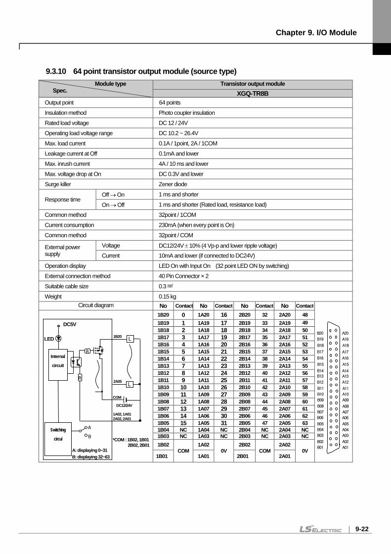
Chapter 9. I/O Module
9-22
9.3.10 64 point transistor output module (source type) Module type
Spec. Transistor output module
XGQ-TR8B Output point 64 points
Insulation method Photo coupler insulation
Rated load voltage DC 12 / 24V
Operating load voltage range DC 10.2 ~ 26.4V
Max. load current 0.1A / 1point, 2A / 1COM
Leakage current at Off 0.1mA and lower
Max. inrush current 4A / 10 ms and lower
Max. voltage drop at On DC 0.3V and lower
Surge killer Zener diode
Response time Off → On 1 ms and shorter
On → Off 1 ms and shorter (Rated load, resistance load)
Common method 32point / 1COM
Current consumption 230mA (when every point is On)
Common method 32point / COM
External power supply
Voltage DC12/24V ± 10% (4 Vp-p and lower ripple voltage) Current 10mA and lower (if connected to DC24V)
Operation display LED On with Input On (32 point LED ON by switching)
External connection method 40 Pin Connector × 2
Suitable cable size 0.3
Weight 0.15 kg Circuit diagram No Contact No Contact No Contact No Contact
1B20 0 1A20 16 2B20 32 2A20 48 1B19 1 1A19 17 2B19 33 2A19 49 1B18 2 1A18 18 2B18 34 2A18 50 1B17 3 1A17 19 2B17 35 2A17 51 1B16 4 1A16 20 2B16 36 2A16 52 1B15 5 1A15 21 2B15 37 2A15 53 1B14 6 1A14 22 2B14 38 2A14 54 1B13 7 1A13 23 2B13 39 2A13 55 1B12 8 1A12 24 2B12 40 2A12 56 1B11 9 1A11 25 2B11 41 2A11 57 1B10 10 1A10 26 2B10 42 2A10 58 1B09 11 1A09 27 2B09 43 2A09 59 1B08 12 1A08 28 2B08 44 2A08 60 1B07 13 1A07 29 2B07 45 2A07 61 1B06 14 1A06 30 2B06 46 2A06 62 1B05 15 1A05 31 2B05 47 2A05 63 1B04 NC 1A04 NC 2B04 NC 2A04 NC 1B03 NC 1A03 NC 2B03 NC 2A03 NC 1B02
COM 1A02
0V 2B02
COM 2A02
0V 1B01 1A01 2B01 2A01
B20
B19
B18
B17
B16
B15
B14
B13
B12
B11
B10
B09
B08
B07
B06
B05
B04
B03
B02
B01
A20
A19
A18
A17
A16
A15
A14
A13
A12
A11
A10
A09
A08
A07
A06
A05
A04
A03
A02
A01
DC5V
R
*COM : 1B02, 1B01 / 2B02, 2B01
Internal
circuit
L LED
1B20
2A05
A: displaying 0~31 B: displaying 32~63
R
DC12/24V
COM
1A02, 1A01 2A02, 2A01
L
Switching
circui
A
B
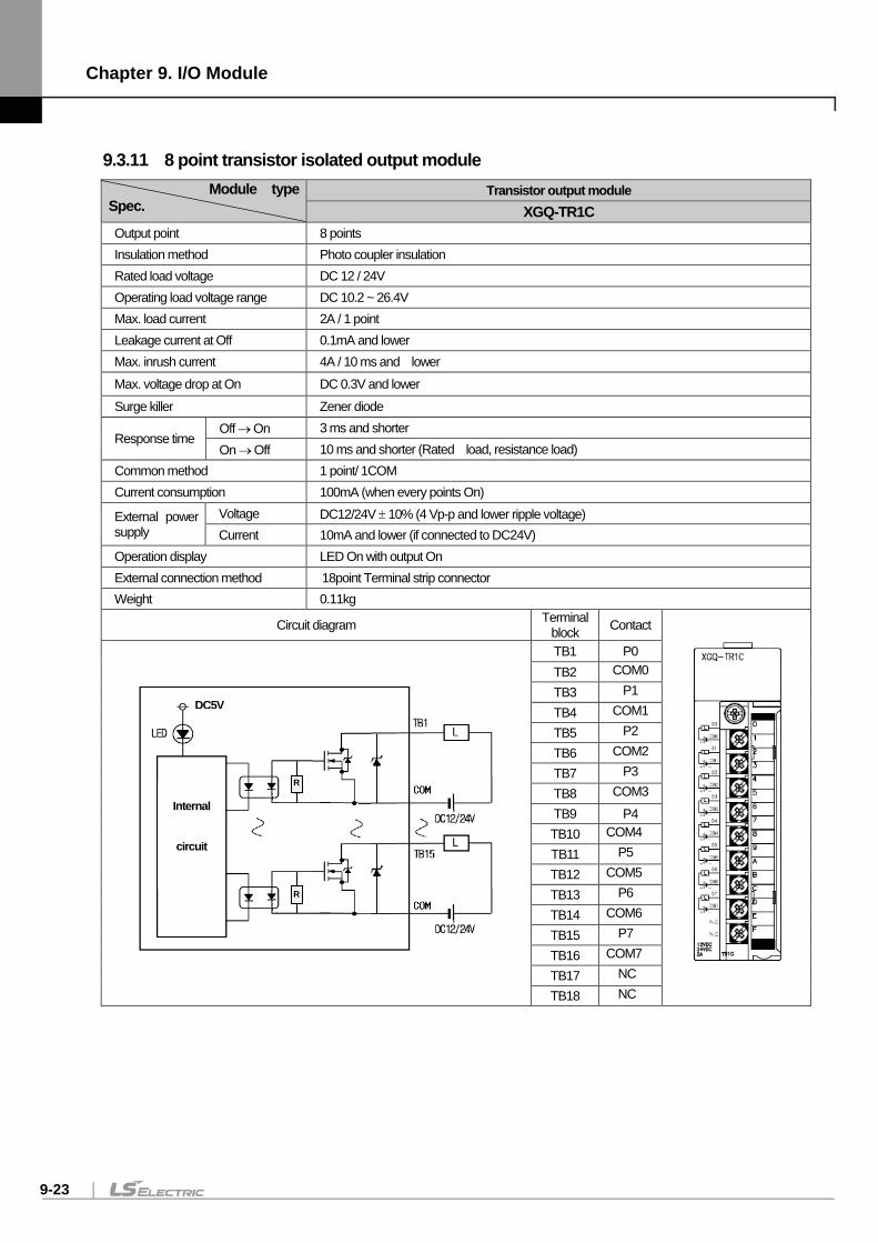
Chapter 9. I/O Module
9-23
9.3.11 8 point transistor isolated output module Module type Spec.
Transistor output module XGQ-TR1C
Output point 8 points Insulation method Photo coupler insulation Rated load voltage DC 12 / 24V Operating load voltage range DC 10.2 ~ 26.4V Max. load current 2A / 1 point Leakage current at Off 0.1mA and lower Max. inrush current 4A / 10 ms and lower Max. voltage drop at On DC 0.3V and lower Surge killer Zener diode
Response time Off → On 3 ms and shorter On → Off 10 ms and shorter (Rated load, resistance load)
Common method 1 point/ 1COM Current consumption 100mA (when every points On)
External power supply
Voltage DC12/24V ± 10% (4 Vp-p and lower ripple voltage) Current 10mA and lower (if connected to DC24V)
Operation display LED On with output On External connection method 18point Terminal strip connector Weight 0.11kg
Circuit diagram Terminal block Contact
TB1 P0 TB2 COM0 TB3 P1 TB4 COM1 TB5 P2 TB6 COM2 TB7 P3 TB8 COM3 TB9 P4 TB10 COM4 TB11 P5 TB12 COM5 TB13 P6 TB14 COM6 TB15 P7 TB16 COM7 TB17 NC TB18 NC
Internal
circuit
R
R
DC5V
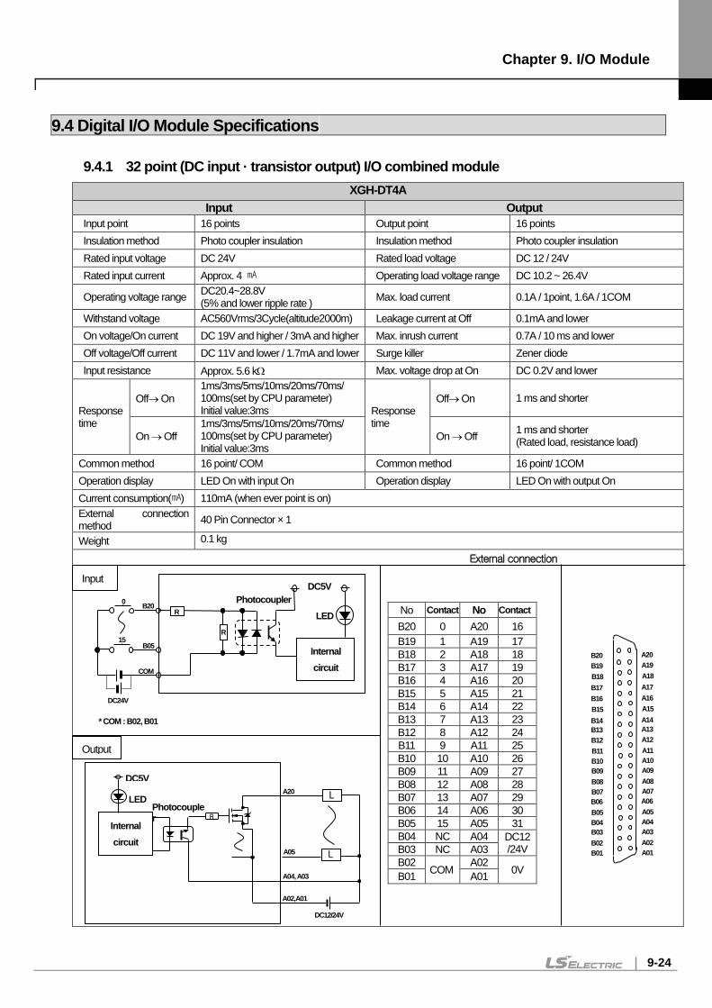
Chapter 9. I/O Module
9-24
9.4 Digital I/O Module Specifications
9.4.1 32 point (DC input · transistor output) I/O combined module XGH-DT4A
Input Output Input point 16 points Output point 16 points Insulation method Photo coupler insulation Insulation method Photo coupler insulation Rated input voltage DC 24V Rated load voltage DC 12 / 24V Rated input current Approx. 4 Operating load voltage range DC 10.2 ~ 26.4V
Operating voltage range DC20.4~28.8V (5% and lower ripple rate ) Max. load current 0.1A / 1point, 1.6A / 1COM
Withstand voltage AC560Vrms/3Cycle(altitude2000m) Leakage current at Off 0.1mA and lower On voltage/On current DC 19V and higher / 3mA and higher Max. inrush current 0.7A / 10 ms and lower Off voltage/Off current DC 11V and lower / 1.7mA and lower Surge killer Zener diode Input resistance Approx. 5.6 kΩ Max. voltage drop at On DC 0.2V and lower
Response time
Off→ On 1ms/3ms/5ms/10ms/20ms/70ms/ 100ms(set by CPU parameter) Initial value:3ms Response
time
Off→ On 1 ms and shorter
On → Off 1ms/3ms/5ms/10ms/20ms/70ms/ 100ms(set by CPU parameter) Initial value:3ms
On → Off 1 ms and shorter (Rated load, resistance load)
Common method 16 point/ COM Common method 16 point/ 1COM Operation display LED On with input On Operation display LED On with output On Current consumption() 110mA (when ever point is on) External connection method 40 Pin Connector × 1
Weight 0.1 kg
No Contact No Contact B20 0 A20 16 B19 1 A19 17 B18 2 A18 18 B17 3 A17 19 B16 4 A16 20 B15 5 A15 21 B14 6 A14 22 B13 7 A13 23 B12 8 A12 24 B11 9 A11 25 B10 10 A10 26 B09 11 A09 27 B08 12 A08 28 B07 13 A07 29 B06 14 A06 30 B05 15 A05 31 B04 NC A04 DC12
/24V B03 NC A03 B02
COM A02
0V B01 A01
B20 B19 B18 B17 B16 B15 B14 B13 B12 B11 B10 B09 B08 B07 B06 B05 B04 B03 B02 B01
A20 A19 A18 A17 A16 A15 A14 A13 A12 A11 A10 A09 A08 A07 A06 A05 A04 A03 A02 A01
External connection
Input
DC24V
Internal circuit
R
15
0
Photocoupler
* COM : B02, B01
COM
R
LED
DC5V
B20
B05
Output
DC12/24V
Photocoupler
R
Internal circuit
A20
A04, A03
A05
A02,A01
DC5V L LED
L
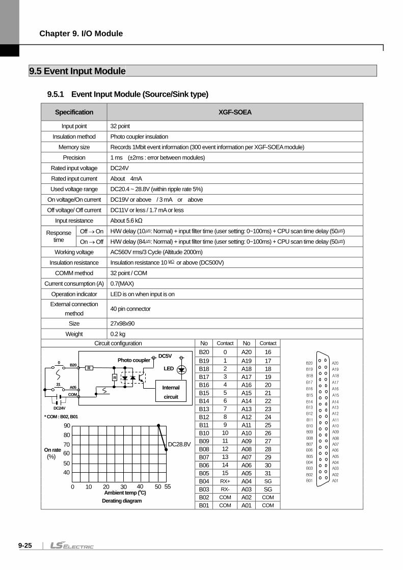
Chapter 9. I/O Module
9-25
9.5 Event Input Module
9.5.1 Event Input Module (Source/Sink type)
Specification XGF-SOEA
Input point 32 point
Insulation method Photo coupler insulation
Memory size Records 1Mbit event information (300 event information per XGF-SOEA module)
Precision 1 ms (±2ms : error between modules)
Rated input voltage DC24V
Rated input current About 4mA
Used voltage range DC20.4 ~ 28.8V (within ripple rate 5%)
On voltage/On current DC19V or above / 3 mA or above
Off voltage/ Off current DC11V or less / 1.7 mA or less
Input resistance About 5.6 kΩ
Response time
Off → On H/W delay (10: Normal) + input filter time (user setting: 0~100ms) + CPU scan time delay (50)
On → Off H/W delay (84: Normal) + input filter time (user setting: 0~100ms) + CPU scan time delay (50)
Working voltage AC560V rms/3 Cycle (Altitude 2000m)
Insulation resistance Insulation resistance 10 or above (DC500V)
COMM method 32 point / COM
Current consumption (A) 0.7(MAX)
Operation indicator LED is on when input is on External connection
method 40 pin connector
Size 27x98x90
Weight 0.2 kg Circuit configuration No Contact No Contact
B20 0 A20 16 B19 1 A19 17 B18 2 A18 18 B17 3 A17 19 B16 4 A16 20 B15 5 A15 21 B14 6 A14 22 B13 7 A13 23 B12 8 A12 24 B11 9 A11 25 B10 10 A10 26 B09 11 A09 27 B08 12 A08 28 B07 13 A07 29 B06 14 A06 30 B05 15 A05 31 B04 RX+ A04 SG B03 RX- A03 SG B02 COM A02 COM B01 COM A01 COM
B20
B19
B18
B17
B16
B15
B14
B13
B12
B11
B10
B09
B08
B07
B06
B05
B04
B03
B02
B01
A20
A19
A18
A17
A16
A15
A14
A13
A12
A11
A10
A09
A08
A07
A06
A05
A04
A03
A02
A01
* COM : B02, B01
DC24V
Internal circuit
R
31
0
B20
COM
Photo coupler
A05
R
DC5V
LED
90
DC28.8V 80
60
40
0 10 20 30 40 50 55
On rate (%)
Ambient temp ()
70
50
Derating diagram
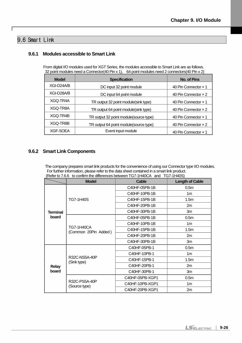
Chapter 9. I/O Module
9-26
9.6 Smart Link
9.6.1 Modules accessible to Smart Link
From digital I/O modules used for XGT Series, the modules accessible to Smart Link are as follows. 32 point modules need a Connector(40 Pin x 1), 64 point modules need 2 connectors(40 Pin x 2)
Model Specification No. of Pins XGI-D24A/B DC input 32 point module 40 Pin Connector × 1 XGI-D28A/B DC input 64 point module 40 Pin Connector × 2 XGQ-TR4A TR output 32 point module(sink type) 40 Pin Connector × 1 XGQ-TR8A TR output 64 point module(sink type) 40 Pin Connector × 2 XGQ-TR4B TR output 32 point module(source type) 40 Pin Connector × 1 XGQ-TR8B TR output 64 point module(source type) 40 Pin Connector × 2 XGF-SOEA Event input module 40 Pin Connector × 1
9.6.2 Smart Link Components
The company prepares smart link products for the convenience of using our Connector type I/O modules. For further information, please refer to the data sheet contained in a smart link product.
(Refer to 7.6.6 1to confirm the differences between TG7-1H40CA 1and 1TG7-1H40S) Model Cable Length of Cable
Terminal board
TG7-1H40S
C40HF-05PB-1B 0.5m C40HF-10PB-1B 1m C40HF-15PB-1B 1.5m C40HF-20PB-1B 2m C40HF-30PB-1B 3m
TG7-1H40CA (Common120Pin1Added )
C40HF-05PB-1B 0.5m C40HF-10PB-1B 1m C40HF-15PB-1B 1.5m C40HF-20PB-1B 2m C40HF-30PB-1B 3m
Relay board
R32C-NS5A-40P (Sink type)
C40HF-05PB-1 0.5m C40HF-10PB-1 1m C40HF-15PB-1 1.5m C40HF-20PB-1 2m C40HF-30PB-1 3m
R32C-PS5A-40P (Source type)
C40HF-05PB-XGP1 0.5m C40HF-10PB-XGP1 1m C40HF-20PB-XGP1 2m
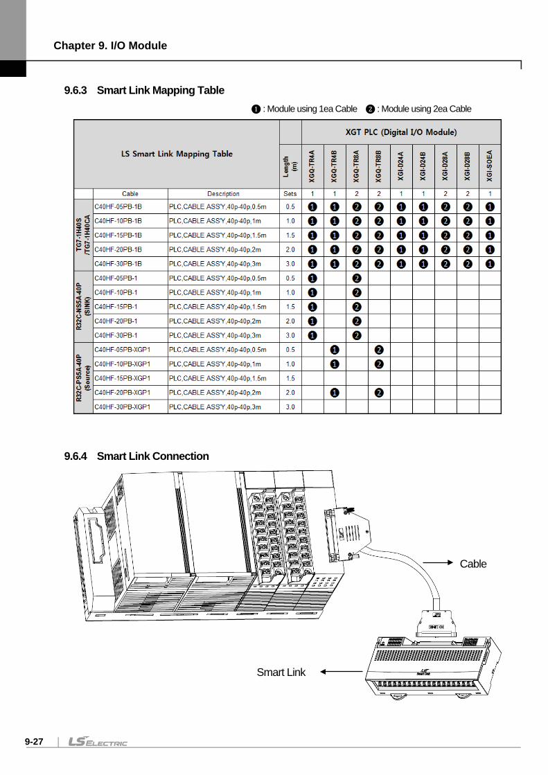
Chapter 9. I/O Module
9-27
9.6.3 Smart Link Mapping Table ❶ : Module using 1ea Cable ❷ : Module using 2ea Cable
9.6.4 Smart Link Connection
Smart Link
Cable
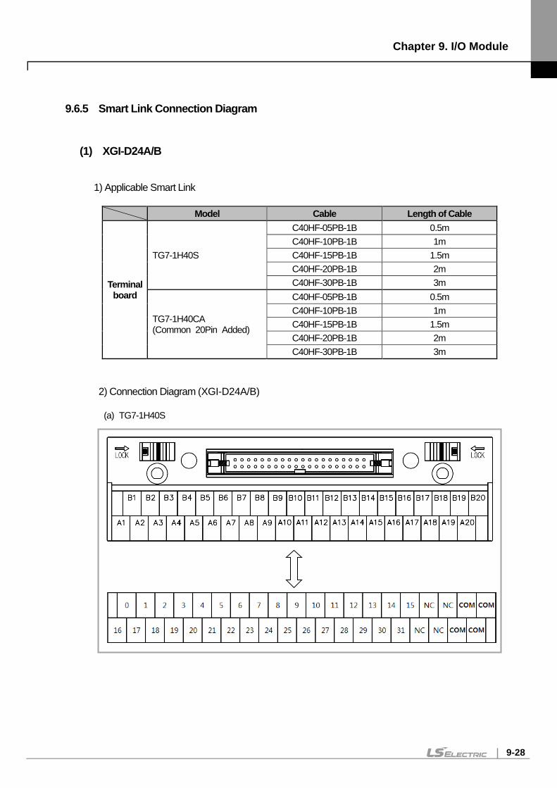
Chapter 9. I/O Module
9-28
9.6.5 Smart Link Connection Diagram
(1) XGI-D24A/B
1) Applicable Smart Link
Model Cable Length of Cable
Terminal board
TG7-1H40S
C40HF-05PB-1B 0.5m C40HF-10PB-1B 1m C40HF-15PB-1B 1.5m C40HF-20PB-1B 2m C40HF-30PB-1B 3m
TG7-1H40CA (Common120Pin1Added)
C40HF-05PB-1B 0.5m C40HF-10PB-1B 1m C40HF-15PB-1B 1.5m C40HF-20PB-1B 2m C40HF-30PB-1B 3m
2) Connection Diagram (XGI-D24A/B)
(a) TG7-1H40S
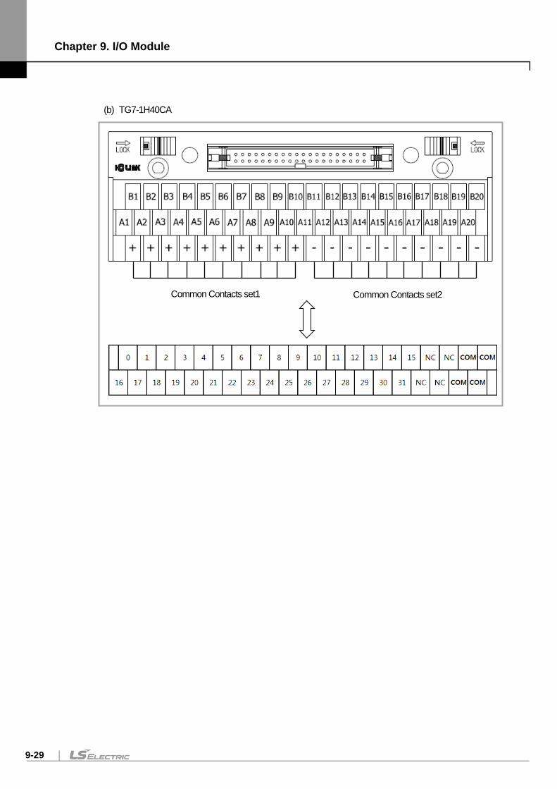
Chapter 9. I/O Module
9-29
(b) TG7-1H40CA
Common Contacts set1 Common Contacts set2
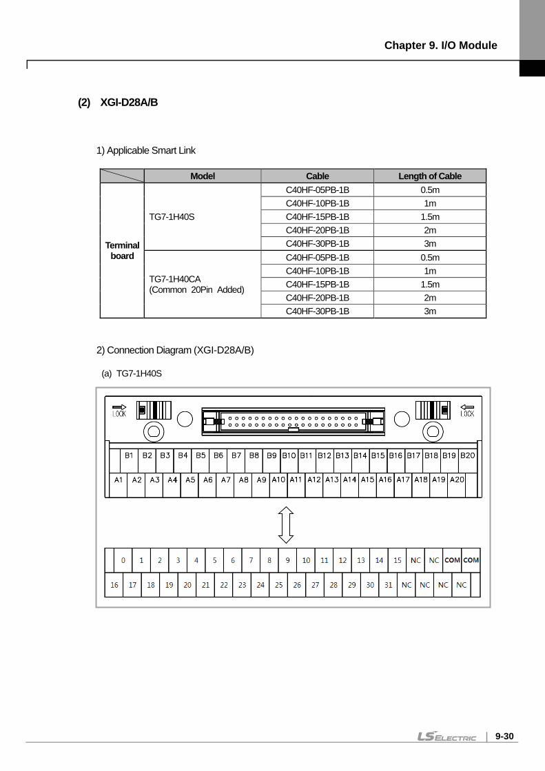
Chapter 9. I/O Module
9-30
(2) XGI-D28A/B
1) Applicable Smart Link
Model Cable Length of Cable
Terminal board
TG7-1H40S
C40HF-05PB-1B 0.5m C40HF-10PB-1B 1m C40HF-15PB-1B 1.5m C40HF-20PB-1B 2m C40HF-30PB-1B 3m
TG7-1H40CA (Common120Pin1Added)
C40HF-05PB-1B 0.5m C40HF-10PB-1B 1m C40HF-15PB-1B 1.5m C40HF-20PB-1B 2m C40HF-30PB-1B 3m
2) Connection Diagram (XGI-D28A/B)
(a) TG7-1H40S
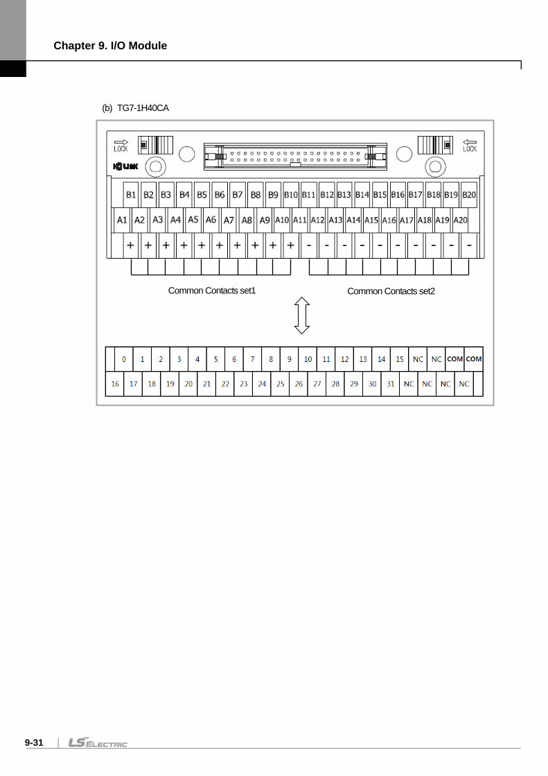
Chapter 9. I/O Module
9-31
(b) TG7-1H40CA
Common Contacts set1 Common Contacts set2
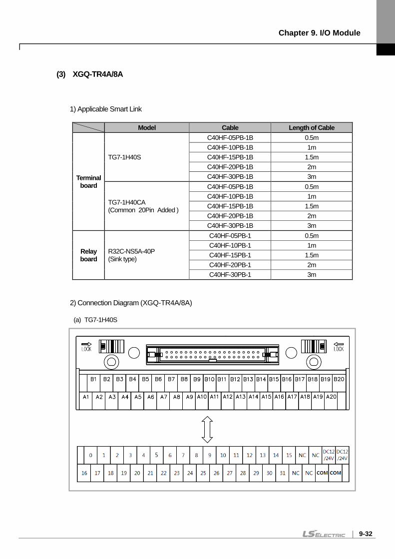
Chapter 9. I/O Module
9-32
(3) XGQ-TR4A/8A
1) Applicable Smart Link
Model Cable Length of Cable
Terminal board
TG7-1H40S
C40HF-05PB-1B 0.5m C40HF-10PB-1B 1m
C40HF-15PB-1B 1.5m
C40HF-20PB-1B 2m
C40HF-30PB-1B 3m
TG7-1H40CA (Common120Pin1Added )
C40HF-05PB-1B 0.5m C40HF-10PB-1B 1m
C40HF-15PB-1B 1.5m
C40HF-20PB-1B 2m
C40HF-30PB-1B 3m
Relay board
R32C-NS5A-40P (Sink type)
C40HF-05PB-1 0.5m C40HF-10PB-1 1m
C40HF-15PB-1 1.5m
C40HF-20PB-1 2m
C40HF-30PB-1 3m
2) Connection Diagram (XGQ-TR4A/8A)
(a) TG7-1H40S
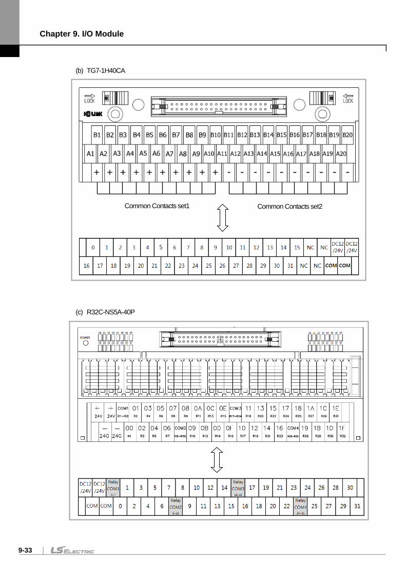
Chapter 9. I/O Module
9-33
(b) TG7-1H40CA
(c) R32C-NS5A-40P
Common Contacts set1 Common Contacts set2
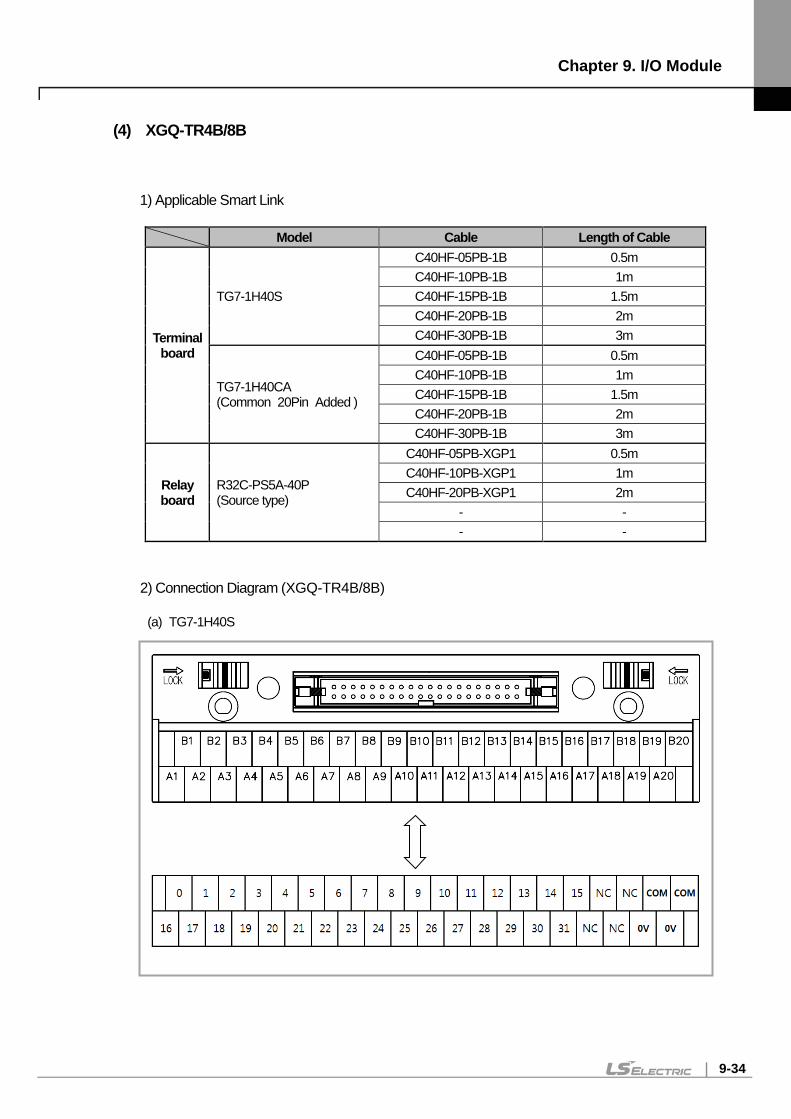
Chapter 9. I/O Module
9-34
(4) XGQ-TR4B/8B
1) Applicable Smart Link
Model Cable Length of Cable
Terminal board
TG7-1H40S
C40HF-05PB-1B 0.5m C40HF-10PB-1B 1m C40HF-15PB-1B 1.5m C40HF-20PB-1B 2m C40HF-30PB-1B 3m
TG7-1H40CA (Common120Pin1Added )
C40HF-05PB-1B 0.5m C40HF-10PB-1B 1m C40HF-15PB-1B 1.5m C40HF-20PB-1B 2m C40HF-30PB-1B 3m
Relay board
R32C-PS5A-40P (Source type)
C40HF-05PB-XGP1 0.5m C40HF-10PB-XGP1 1m C40HF-20PB-XGP1 2m
- - - -
2) Connection Diagram (XGQ-TR4B/8B)
(a) TG7-1H40S
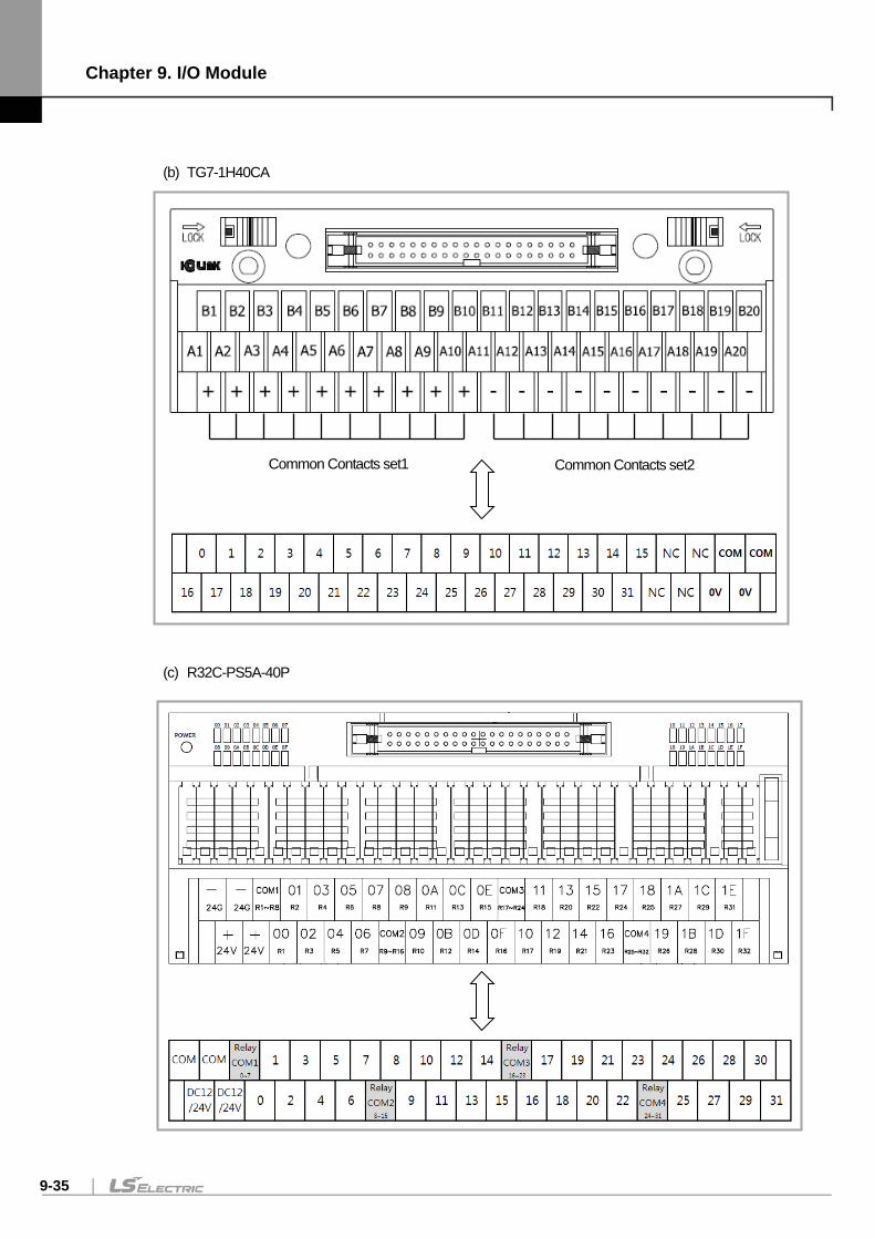
Chapter 9. I/O Module
9-35
(b) TG7-1H40CA
(c) R32C-PS5A-40P
Common Contacts set1 Common Contacts set2
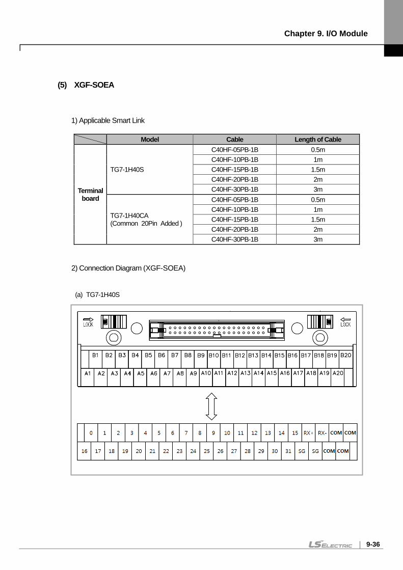
Chapter 9. I/O Module
9-36
(5) XGF-SOEA
1) Applicable Smart Link
Model Cable Length of Cable
Terminal board
TG7-1H40S
C40HF-05PB-1B 0.5m C40HF-10PB-1B 1m
C40HF-15PB-1B 1.5m
C40HF-20PB-1B 2m
C40HF-30PB-1B 3m
TG7-1H40CA (Common120Pin1Added )
C40HF-05PB-1B 0.5m C40HF-10PB-1B 1m
C40HF-15PB-1B 1.5m
C40HF-20PB-1B 2m
C40HF-30PB-1B 3m
2) Connection Diagram (XGF-SOEA)
(a) TG7-1H40S
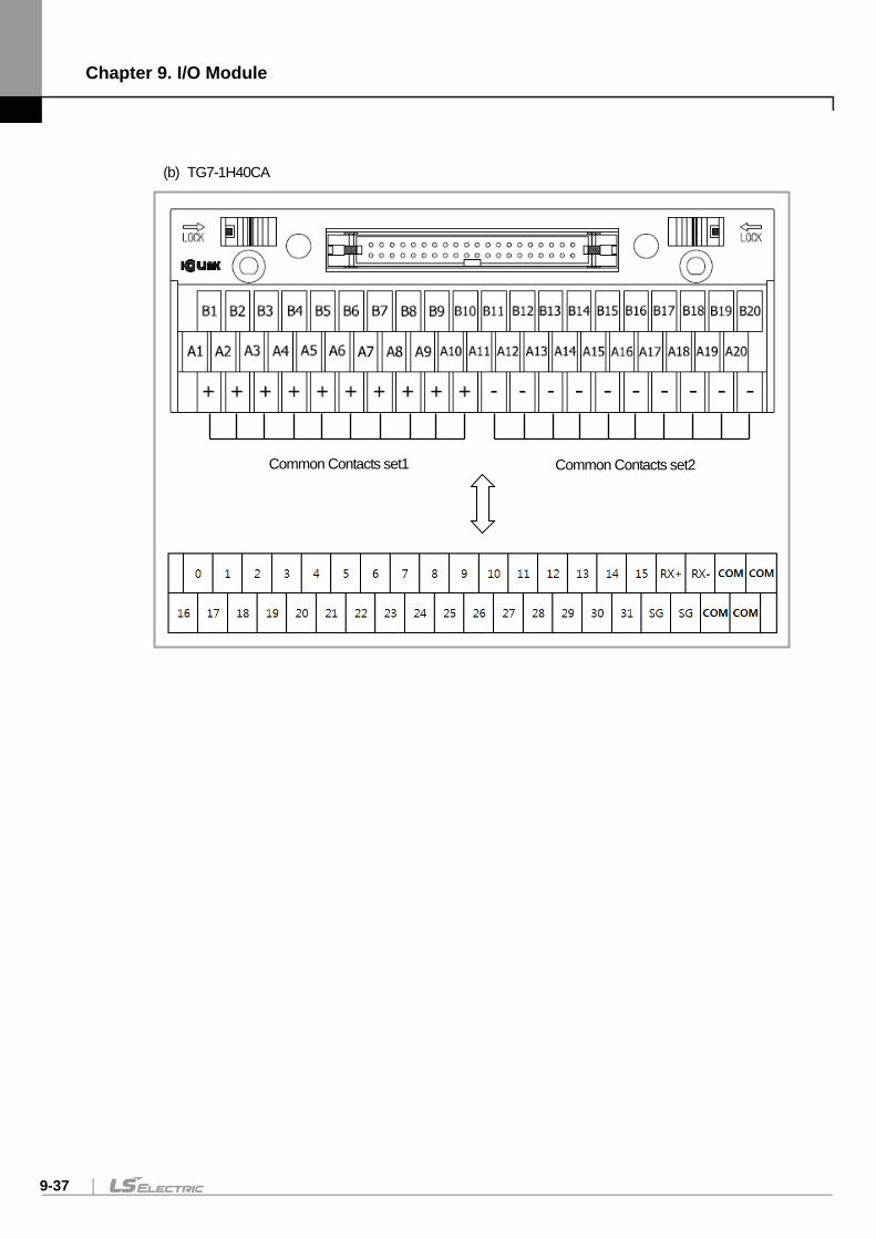
Chapter 9. I/O Module
9-37
(b) TG7-1H40CA
Common Contacts set1 Common Contacts set2
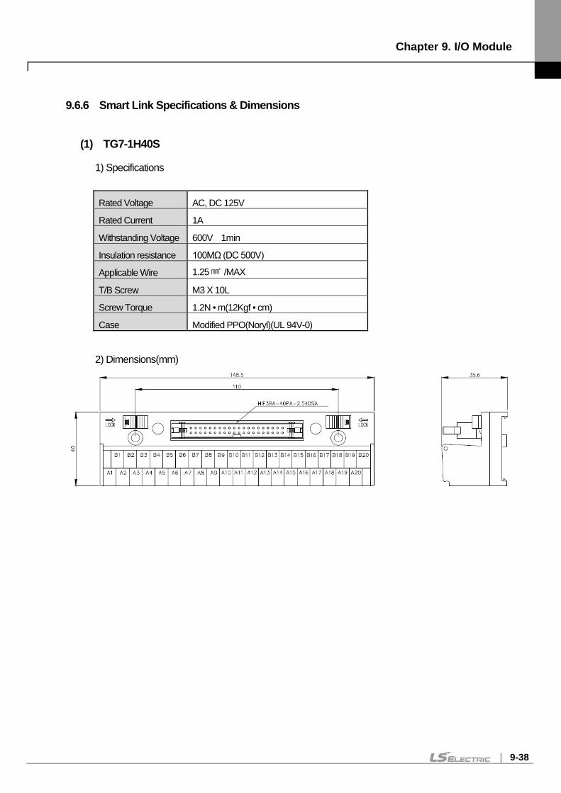
Chapter 9. I/O Module
9-38
9.6.6 Smart Link Specifications & Dimensions
(1) TG7-1H40S
1) Specifications
Rated Voltage AC, DC 125V
Rated Current 1A
Withstanding Voltage 600V 1min
Insulation resistance 100MΩ (DC 500V)
Applicable Wire 1.25 /MAX
T/B Screw M3 X 10L
Screw Torque 1.2N • m(12Kgf • cm)
Case Modified PPO(Noryl)(UL 94V-0)
2) Dimensions(mm)
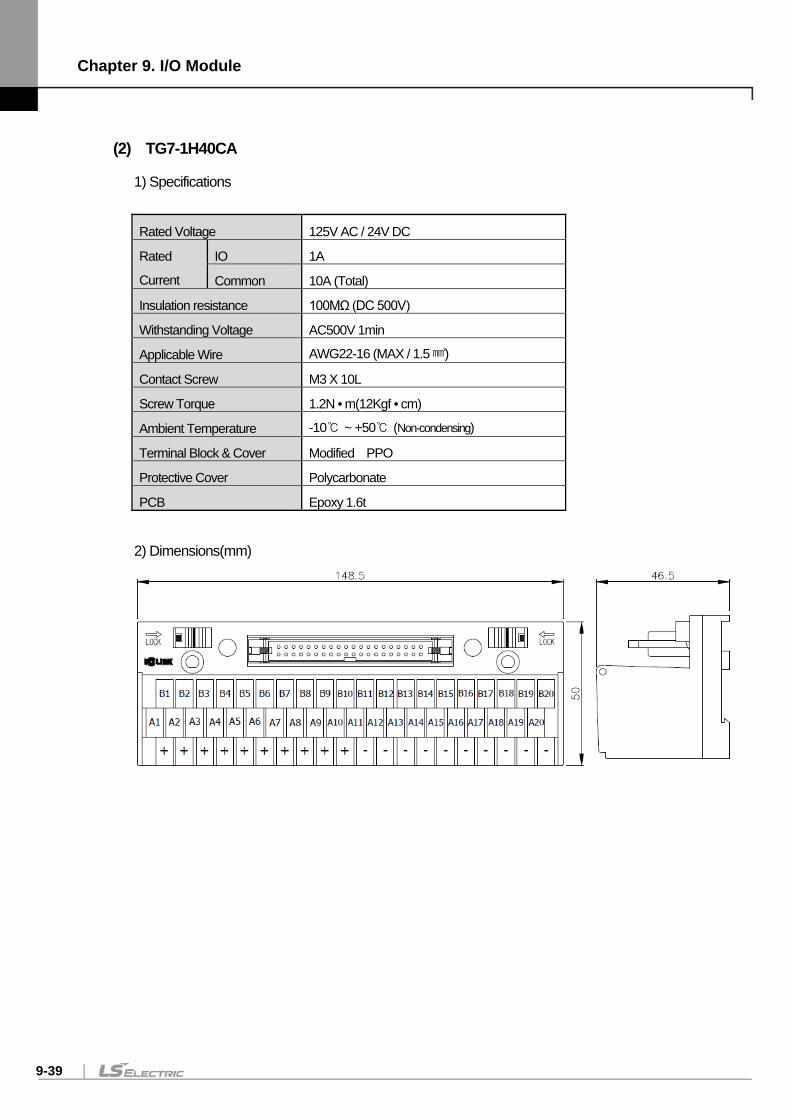
Chapter 9. I/O Module
9-39
(2) TG7-1H40CA
1) Specifications
Rated Voltage 125V AC / 24V DC
Rated
Current
IO 1A
Common 10A (Total)
Insulation resistance 100MΩ (DC 500V)
Withstanding Voltage AC500V 1min
Applicable Wire AWG22-16 (MAX / 1.5)
Contact Screw M3 X 10L
Screw Torque 1.2N • m(12Kgf • cm)
Ambient Temperature -10 ~ +50 (Non-condensing)
Terminal Block & Cover Modified PPO
Protective Cover Polycarbonate
PCB Epoxy 1.6t
2) Dimensions(mm)
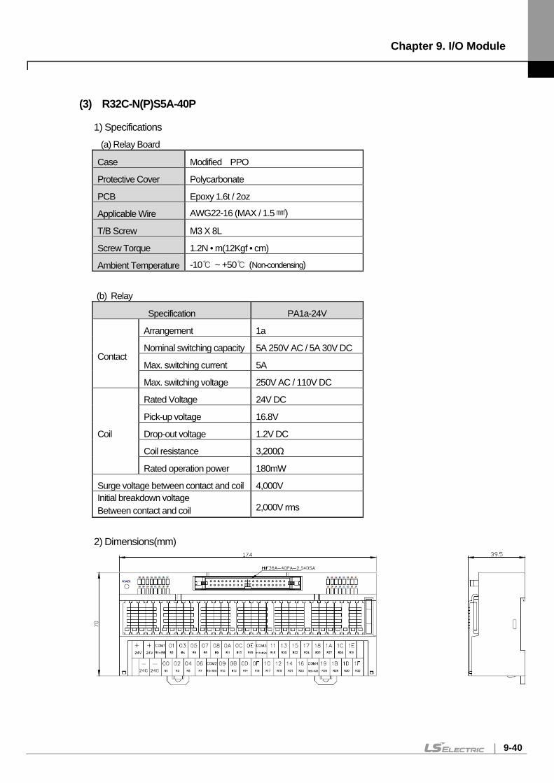
Chapter 9. I/O Module
9-40
(3) R32C-N(P)S5A-40P
1) Specifications (a) Relay Board
Case Modified PPO
Protective Cover Polycarbonate
PCB Epoxy 1.6t / 2oz
Applicable Wire AWG22-16 (MAX / 1.5)
T/B Screw M3 X 8L
Screw Torque 1.2N • m(12Kgf • cm)
Ambient Temperature -10 ~ +50 (Non-condensing)
(b) Relay
Specification PA1a-24V
Contact
Arrangement 1a
Nominal switching capacity 5A 250V AC / 5A 30V DC
Max. switching current 5A
Max. switching voltage 250V AC / 110V DC
Coil
Rated Voltage 24V DC
Pick-up voltage 16.8V
Drop-out voltage 1.2V DC
Coil resistance 3,200Ω
Rated operation power 180mW
Surge voltage between contact and coil 4,000V Initial breakdown voltage Between contact and coil 2,000V rms
2) Dimensions(mm)
Chapter 10. Base and Expansion Cable
10-1
Chapter 10 Base and Expansion Cable
10.1 Specification
10.1.1 Basic base Power module, CPU module, Ethernet communication module can be inserted into basic base.
XGR-M02P/XGR-M06P uses 5.5A output power module.
Table 1 Specification of basic base
Name
Item XGR-M02P XGR-M06P
The no. of IO module 2 modules 6 modules
Dimension (mm) 238 X 98 X 19 346 X 98 X 19
Distance of hole for panel attachment 218 X 75 326 X 75
Specification of hole for panel attachment φ 4.5 (M4 screw used)
Specification of screw for PE connection (+)PHM 3 X 6 washer(φ 5)
Weight (kg) 0.33 0.5
10.1.2 Expansion Base Power module, expansion driver module, IO module, special module, communication module can be inserted into expansion
base.
Table 2 Specification of expansion base
Name
Item XGR-E12P XGR-E08P XGR-E12H
The no. of IO module 12 modules 8 modules 12 modules
Dimension (mm) 481 X 98 X 19 373 X 98 X 19 508 X 98 X 19
Distance of hole for
panel attachment 461 X 75 353 X 75 488 X 75
Specification of hole
for panel attachment φ 4.5 (M4 screw used)
Specification of screw
for PE connection (+)PHM 3 X 6 washer (φ 5)
Weight (kg) (kg) 0.7 0.51 0.71
Chapter 10. Base and Expansion Cable
10-2
10.1.3 Sync. Cable This cable is used for the data synchronization between CPU modules.
Table 3 Specification of Sync. cable
Name
Item XGC-F201 XGC-F501
Length (m) 2.0 5.0
Weight (g) 21g 47g
Connector LC type
Optical fiber
diameter 62.5/125um(62.5um fiber optic core and 125um outer cladding)
Wave length 1300nm
Attenuation 1.3Db/1000m or less
The quality of the
material Multi Mode Fiber (max. 2 Km) – separate order for other specifications
10.1.4 Expansion Cable This is the cable for connecting the basic and expansion bases. These are Ethernet cables. Electrical and optical cables are
provided for use in accordance with the network type.
Especially, since the electrical cables transmit control data by tens of micro, external noise may affect system performance
and control seriously.
Therefore, when using electrical cables in the XGR system, the FTP cable is the standard. If the system is subject to serious
noise environment, use shielded twisted pair cable, such as STP/FSTP.
Caution 1) The length of the optical cables should not exceed 2Km. 2) The length of the electrical cables should not exceed 100m.
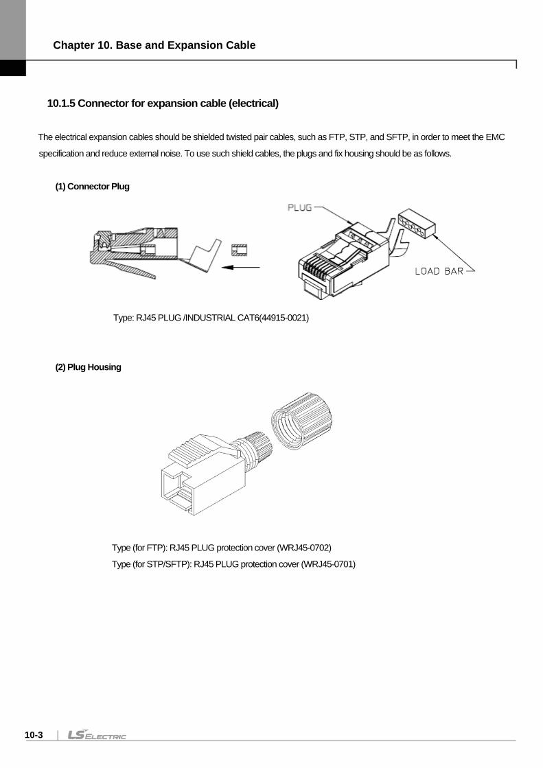
Chapter 10. Base and Expansion Cable
10-3
10.1.5 Connector for expansion cable (electrical)
The electrical expansion cables should be shielded twisted pair cables, such as FTP, STP, and SFTP, in order to meet the EMC
specification and reduce external noise. To use such shield cables, the plugs and fix housing should be as follows.
(1) Connector Plug
Type: RJ45 PLUG /INDUSTRIAL CAT6(44915-0021)
(2) Plug Housing
Type (for FTP): RJ45 PLUG protection cover (WRJ45-0702)
Type (for STP/SFTP): RJ45 PLUG protection cover (WRJ45-0701)
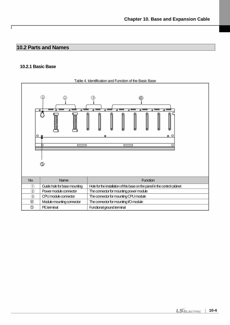
Chapter 10. Base and Expansion Cable
10-4
10.2 Parts and Names
10.2.1 Basic Base
Table 4. Identification and Function of the Basic Base
No. Name Function ① Guide hole for base mounting Hole for the installation of this base on the panel in the control cabinet ② Power module connector The connector for mounting power module ③ CPU module connector The connector for mounting CPU module
Module mounting connector The connector for mounting I/O module PE terminal Functional ground terminal
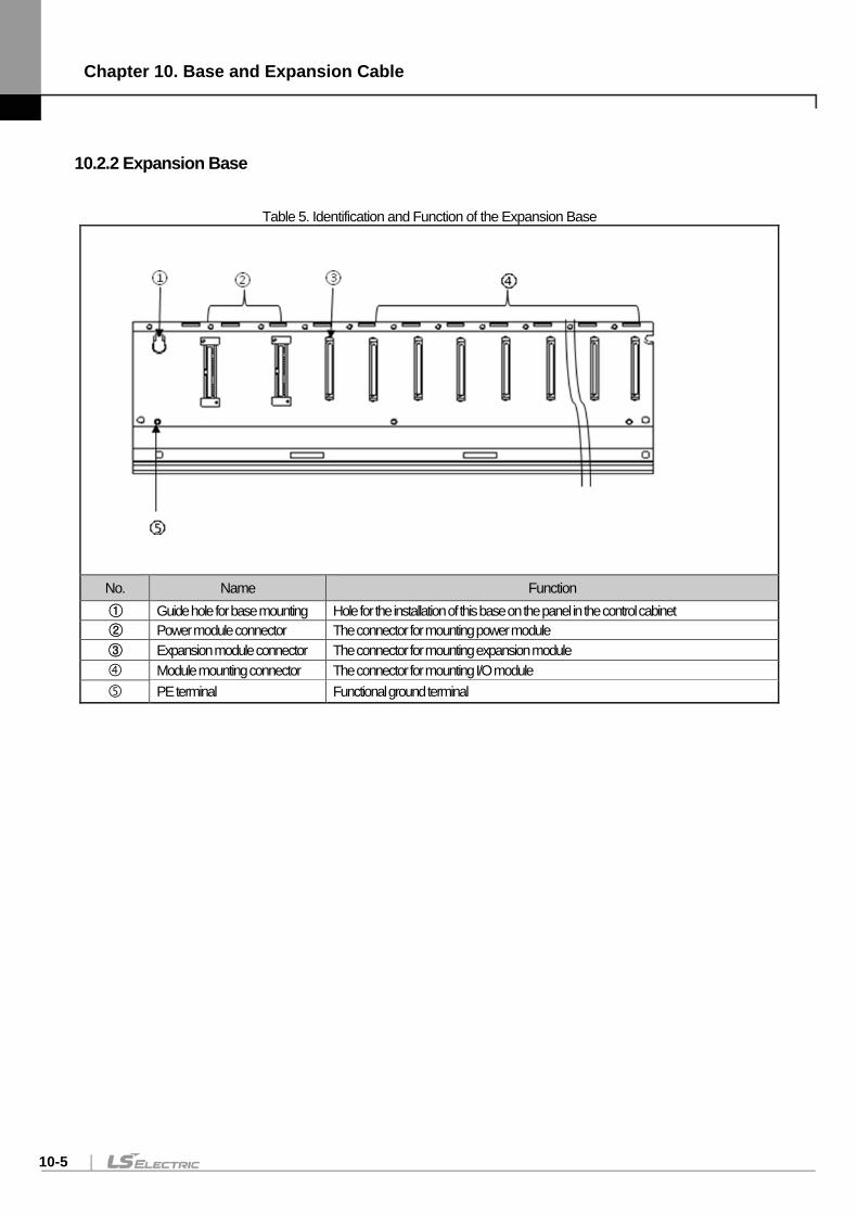
Chapter 10. Base and Expansion Cable
10-5
10.2.2 Expansion Base
Table 5. Identification and Function of the Expansion Base
No. Name Function ① Guide hole for base mounting Hole for the installation of this base on the panel in the control cabinet ② Power module connector The connector for mounting power module
/③ Expansion module connector The connector for mounting expansion module Module mounting connector The connector for mounting I/O module PE terminal Functional ground terminal

Chapter 10. Base and Expansion Cable
10-6
Chapter 11. Installation and Wiring
11-1
Chapter 11. Installation and Wiring
11.1 Installation
11.1.1 Installation environment The system keeps a high reliability, irrespective of the installation environment. However, to guarantee the reliability and stability, make sure to keep the following cautions. (1) Environmental conditions
(a) Install in a control panel resisting to moisture and vibration. (b) Free of any continuous impact or vibration. (c) Not exposed to direct sunrays. (d) No condensation from sudden temperature fluctuation. (e) Ambient temperature range between 0 ~ 55°C. (f) Relative humidity between 5 ~ 95%. (g) Free of any corrosive gas or flammable gas. (h) The falling of a thunderbolt and high voltage should not flow in
(2) Installation construction (a) When boring a screw hole or executing wiring construction, any wiring impurities should not be inserted to the
PLC. (b) The system should be installed in a place easily accessible. (c) Do not install the system on a same panel of a high voltage device. (d) It should be 50mm and more away from wiring duct or proximate modules. (e) Grounding on a position where noise is lower than the specified level.
(3) Heat protective design of control panel (a) If installing the PLC in an air-tight control panel, it needs heat-protective(control) design considering the heat
from the PLC as well as other devices. If ventilating by vent or fan, inflow of dust or gas may affect the performance of the PLC system.
(b) Install a filter or use a closed heat exchanger.
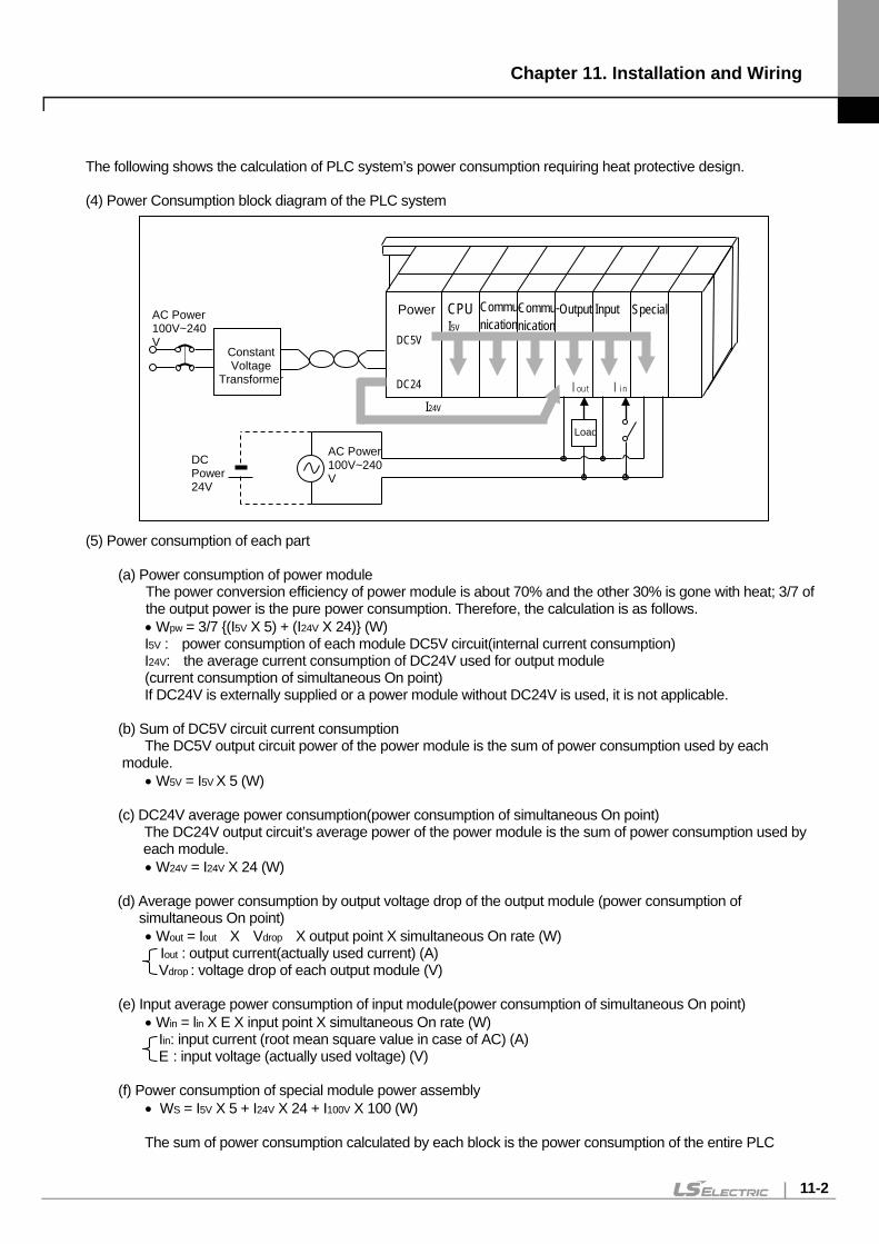
Chapter 11. Installation and Wiring
11-2
The following shows the calculation of PLC system’s power consumption requiring heat protective design. (4) Power Consumption block diagram of the PLC system (5) Power consumption of each part
(a) Power consumption of power module
The power conversion efficiency of power module is about 70% and the other 30% is gone with heat; 3/7 of the output power is the pure power consumption. Therefore, the calculation is as follows. • Wpw = 3/7 (I5V X 5) + (I24V X 24) (W) I5V : power consumption of each module DC5V circuit(internal current consumption) I24V: the average current consumption of DC24V used for output module (current consumption of simultaneous On point) If DC24V is externally supplied or a power module without DC24V is used, it is not applicable.
(b) Sum of DC5V circuit current consumption The DC5V output circuit power of the power module is the sum of power consumption used by each
module. • W5V = I5V X 5 (W)
(c) DC24V average power consumption(power consumption of simultaneous On point) The DC24V output circuit’s average power of the power module is the sum of power consumption used by each module. • W24V = I24V X 24 (W)
(d) Average power consumption by output voltage drop of the output module (power consumption of simultaneous On point) • Wout = Iout X Vdrop X output point X simultaneous On rate (W)
Iout : output current(actually used current) (A) Vdrop : voltage drop of each output module (V)
(e) Input average power consumption of input module(power consumption of simultaneous On point)
• Win = lin X E X input point X simultaneous On rate (W) Iin: input current (root mean square value in case of AC) (A) E : input voltage (actually used voltage) (V)
(f) Power consumption of special module power assembly
• WS = I5V X 5 + I24V X 24 + I100V X 100 (W) The sum of power consumption calculated by each block is the power consumption of the entire PLC
Power CPU
Constant Voltage
Transformer
AC Power 100V~240V
Commu- nication
Output Input Special
DC5V
DC24
Load
Iout Iin
I5V
I24V
AC Power 100V~240V
DC Power 24V
Commu- nication
Chapter 11. Installation and Wiring
11-3
system. • W = WPW + W5V + W24V + Wout + Win + Ws (W) Calculate the heats according to the entire power consumption(W) and review the temperature increase within the control panel. The calculation of temperature rise within the control panel is displayed as follows. T = W / UA [°C]
W : power consumption of the entire PLC system (the above calculated value) A : surface area of control panel [m2] U : if equalizing the temperature of the control panel by using a fan and others - - - 6 If the air inside the panel is not ventilated - - - - - - - - - - 4
Note
(1) If the control cabinet is not well ventilated, temperature gradient in the cabinet may be large. Care must be taken that the parts right above heat generating devices may become very hot. (2) Coefficient U, which can be different according to quantity of material, is general example
Calculation example) Redundant basic base: 4 communication modules equipped Expansion base 1: optical expansion drive, 6 Input modules, 6 output modules Expansion base 2:optical expansion drive, 6 analog input modules, 6 analog output modules. Structure figure, calculation according to above steps
11.1.2 Cautions for handling It describes the cautions for handling from unpacking to installation.
• Please do not drop it or apply excessive force on it. • Please do not separate PCB from the case. It may cause a trouble. • During wiring, a special attention should be paid so that impurities such as wiring remainder should not be
inserted into the top of a module. If impurities are found, immediately remove them. (1) Cautions for handling I/O module
It describes the cautions for installing or handling I/O module. (a) Recheck the I/O module specifications.
The input module may be affected by input voltage while the output module may be subject to breakage, destruction or a fire if the voltage over the max. switching capacity is allowed.
(b) Available cable type Cable should be selected in consideration of ambient temperature and allowable current; the min. size of cable should be AWG22(0.3mm2) and higher.
(c) Environment If I/O module wiring is close to heating sources or materials or the wiring is directly contacted with oils for a long time during wiring, it may cause short-circuit, destruction or malfunction.
(d) Polarities Please make sure to check the polarities of modules of which terminal block is polarized before allowing the
power.
(e) Wiring
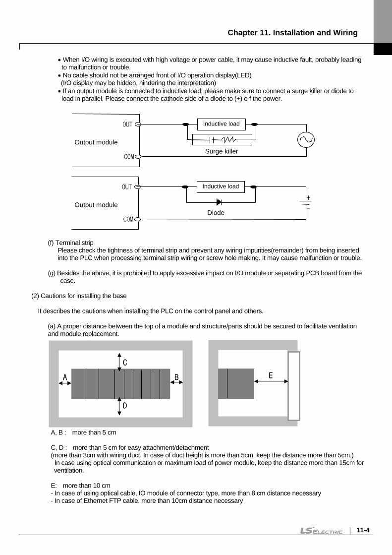
Chapter 11. Installation and Wiring
11-4
• When I/O wiring is executed with high voltage or power cable, it may cause inductive fault, probably leading to malfunction or trouble. • No cable should not be arranged front of I/O operation display(LED) (I/O display may be hidden, hindering the interpretation) • If an output module is connected to inductive load, please make sure to connect a surge killer or diode to load in parallel. Please connect the cathode side of a diode to (+) o f the power.
(f) Terminal strip
Please check the tightness of terminal strip and prevent any wiring impurities(remainder) from being inserted into the PLC when processing terminal strip wiring or screw hole making. It may cause malfunction or trouble.
(g) Besides the above, it is prohibited to apply excessive impact on I/O module or separating PCB board from the case.
(2) Cautions for installing the base
It describes the cautions when installing the PLC on the control panel and others.
(a) A proper distance between the top of a module and structure/parts should be secured to facilitate ventilation and module replacement.
A, B : more than 5 cm
C, D : more than 5 cm for easy attachment/detachment (more than 3cm with wiring duct. In case of duct height is more than 5cm, keep the distance more than 5cm.) In case using optical communication or maximum load of power module, keep the distance more than 15cm for ventilation.
E: more than 10 cm - In case of using optical cable, IO module of connector type, more than 8 cm distance necessary - In case of Ethernet FTP cable, more than 10cm distance necessary
OUT
COM
Output module
Inductive load
Surge killer
OUT
COM
Output module
Inductive load
Diode
+
-
A B
C
D
E
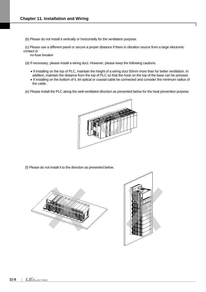
Chapter 11. Installation and Wiring
11-5
(b) Please do not install it vertically or horizontally for the ventilation purpose. (c) Please use a different panel or secure a proper distance if there is vibration source from a large electronic
contact or no-fuse breaker
(d) If necessary, please install a wiring duct. However, please keep the following cautions.
• If installing on the top of PLC, maintain the height of a wiring duct 50mm more than for better ventilation. In addition, maintain the distance from the top of PLC so that the hook on the top of the base can be pressed. • If installing on the bottom of it, let optical or coaxial cable be connected and consider the minimum radius of the cable.
(e) Please install the PLC along the well-ventilated direction as presented below for the heat prevention purpose.
(f) Please do not install it to the direction as presented below.
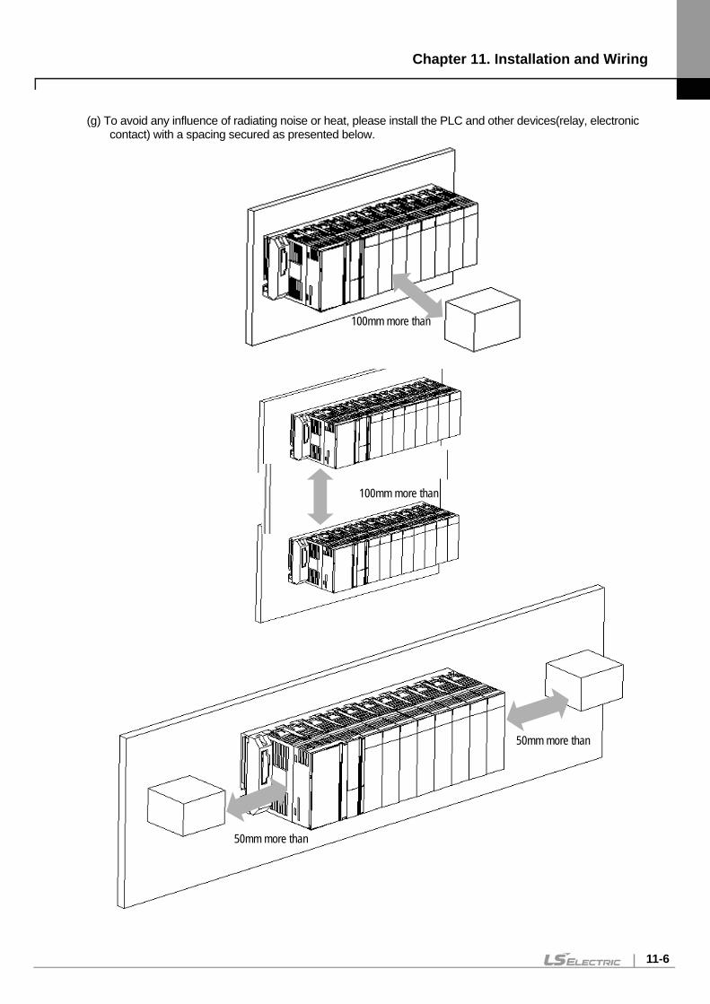
Chapter 11. Installation and Wiring
11-6
(g) To avoid any influence of radiating noise or heat, please install the PLC and other devices(relay, electronic
contact) with a spacing secured as presented below.
50mm more than
50mm more than
100mm more than
100mm more than
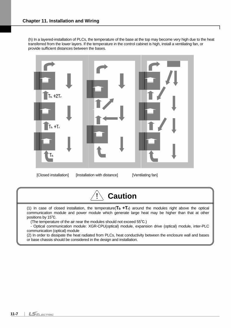
Chapter 11. Installation and Wiring
11-7
(h) In a layered-installation of PLCs, the temperature of the base at the top may become very high due to the heat transferred from the lower layers. If the temperature in the control cabinet is high, install a ventilating fan, or provide sufficient distances between the bases.
[Closed installation] [Installation with distance] [Ventilating fan]
Tb
Tb +Tr
Tb +2Tr
(1) In case of closed installation, the temperature(Tb +Tr) around the modules right above the optical communication module and power module which generate large heat may be higher than that at other positions by 15.
(The temperature of the air near the modules should not exceed 55.) - Optical communication module: XGR-CPU(optical) module, expansion drive (optical) module, inter-PLC
communication (optical) module (2) In order to dissipate the heat radiated from PLCs, heat conductivity between the enclosure wall and bases or base chassis should be considered in the design and installation.
Caution
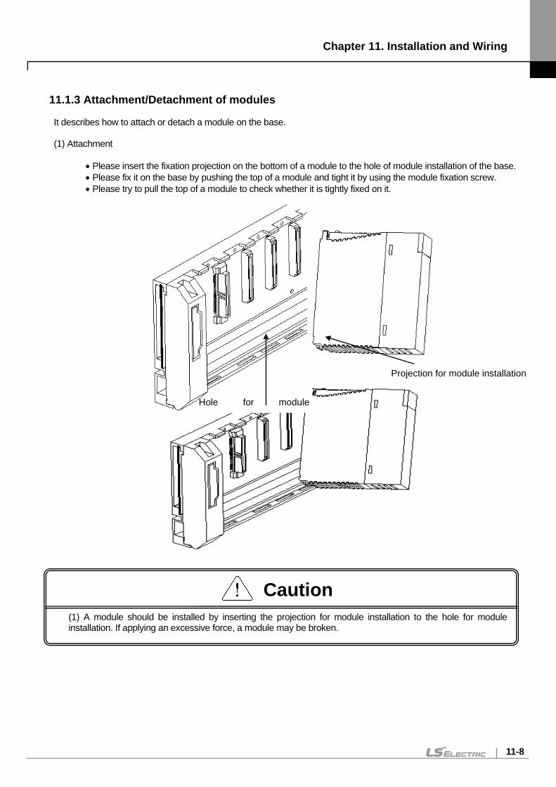
Chapter 11. Installation and Wiring
11-8
11.1.3 Attachment/Detachment of modules It describes how to attach or detach a module on the base. (1) Attachment
• Please insert the fixation projection on the bottom of a module to the hole of module installation of the base. • Please fix it on the base by pushing the top of a module and tight it by using the module fixation screw. • Please try to pull the top of a module to check whether it is tightly fixed on it.
Hole for module
Projection for module installation
(1) A module should be installed by inserting the projection for module installation to the hole for module installation. If applying an excessive force, a module may be broken.
Caution
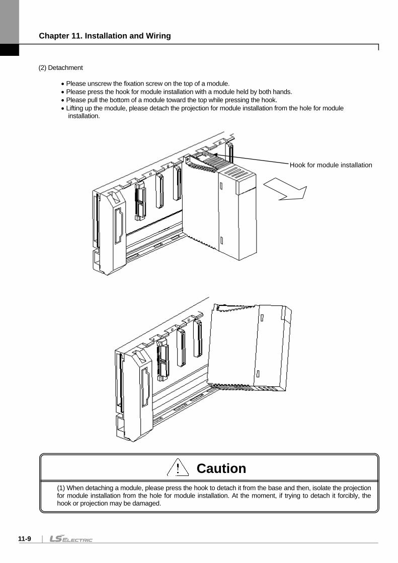
Chapter 11. Installation and Wiring
11-9
(2) Detachment
• Please unscrew the fixation screw on the top of a module. • Please press the hook for module installation with a module held by both hands. • Please pull the bottom of a module toward the top while pressing the hook. • Lifting up the module, please detach the projection for module installation from the hole for module
installation.
Hook for module installation
(1) When detaching a module, please press the hook to detach it from the base and then, isolate the projection for module installation from the hole for module installation. At the moment, if trying to detach it forcibly, the hook or projection may be damaged.
Caution
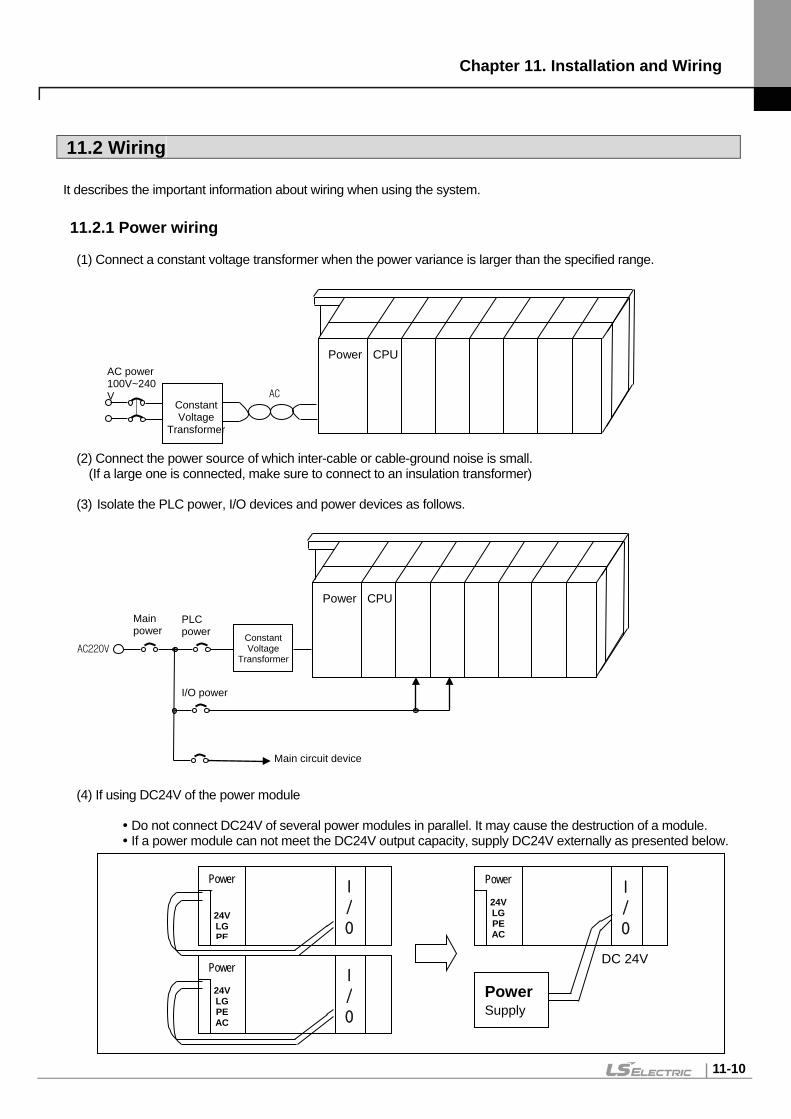
Chapter 11. Installation and Wiring
11-10
11.2 Wiring It describes the important information about wiring when using the system.
11.2.1 Power wiring (1) Connect a constant voltage transformer when the power variance is larger than the specified range.
(2) Connect the power source of which inter-cable or cable-ground noise is small. (If a large one is connected, make sure to connect to an insulation transformer) (3) Isolate the PLC power, I/O devices and power devices as follows.
(4) If using DC24V of the power module
Do not connect DC24V of several power modules in parallel. It may cause the destruction of a module. If a power module can not meet the DC24V output capacity, supply DC24V externally as presented below.
Power CPU
AC
Constant Voltage
Transformer
AC power 100V~240V
Power
CPU
AC220V
Main power
Constant Voltage
Transformer
PLC power
Main circuit device
I/O power
Powerr
24V LG PE
I
/
O
Power
24V LG PE AC
I
/
O
Power Supply
DC 24V Power
24V LG PE AC
I
/
O
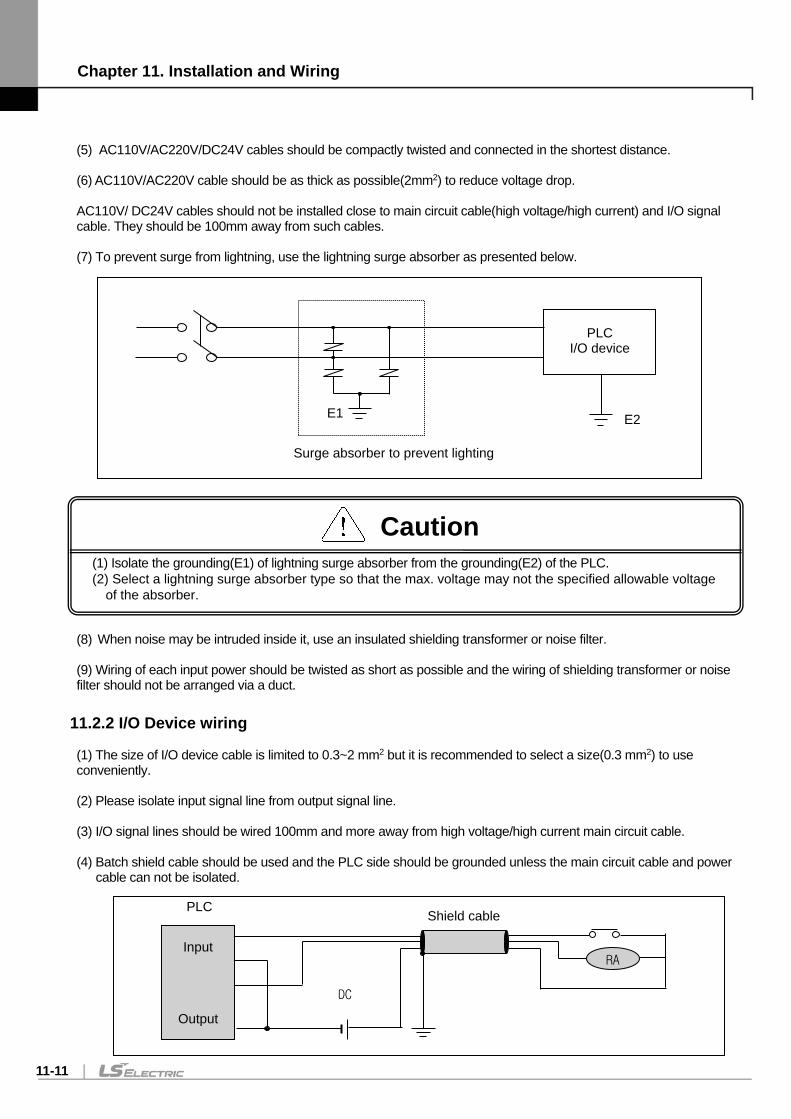
Chapter 11. Installation and Wiring
11-11
(5) AC110V/AC220V/DC24V cables should be compactly twisted and connected in the shortest distance. (6) AC110V/AC220V cable should be as thick as possible(2mm2) to reduce voltage drop. AC110V/ DC24V cables should not be installed close to main circuit cable(high voltage/high current) and I/O signal cable. They should be 100mm away from such cables. (7) To prevent surge from lightning, use the lightning surge absorber as presented below.
(8) When noise may be intruded inside it, use an insulated shielding transformer or noise filter. (9) Wiring of each input power should be twisted as short as possible and the wiring of shielding transformer or noise filter should not be arranged via a duct.
11.2.2 I/O Device wiring (1) The size of I/O device cable is limited to 0.3~2 mm2 but it is recommended to select a size(0.3 mm2) to use conveniently. (2) Please isolate input signal line from output signal line. (3) I/O signal lines should be wired 100mm and more away from high voltage/high current main circuit cable. (4) Batch shield cable should be used and the PLC side should be grounded unless the main circuit cable and power
cable can not be isolated.
Input
Output
PLC Shield cable
RA
DC
E2
PLC I/O device
E1
Surge absorber to prevent lighting
(1) Isolate the grounding(E1) of lightning surge absorber from the grounding(E2) of the PLC. (2) Select a lightning surge absorber type so that the max. voltage may not the specified allowable voltage
of the absorber.
Caution
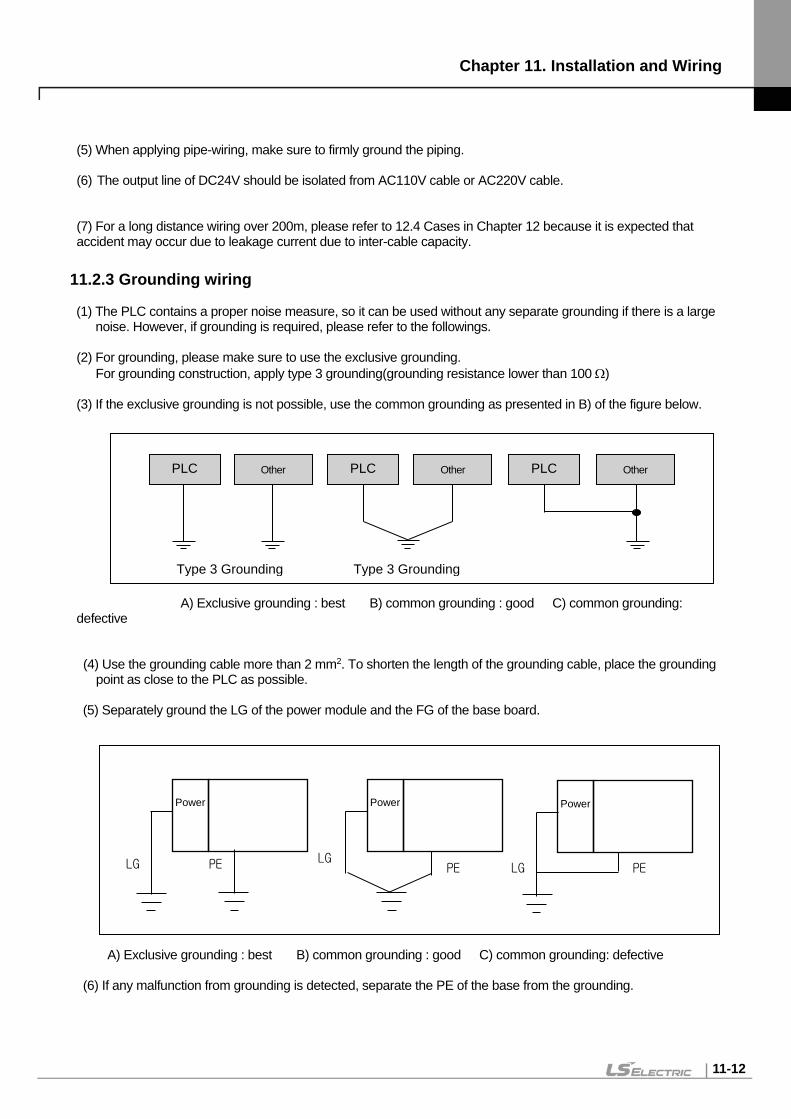
Chapter 11. Installation and Wiring
11-12
(5) When applying pipe-wiring, make sure to firmly ground the piping. (6) The output line of DC24V should be isolated from AC110V cable or AC220V cable. (7) For a long distance wiring over 200m, please refer to 12.4 Cases in Chapter 12 because it is expected that accident may occur due to leakage current due to inter-cable capacity.
11.2.3 Grounding wiring (1) The PLC contains a proper noise measure, so it can be used without any separate grounding if there is a large
noise. However, if grounding is required, please refer to the followings. (2) For grounding, please make sure to use the exclusive grounding.
For grounding construction, apply type 3 grounding(grounding resistance lower than 100 Ω) (3) If the exclusive grounding is not possible, use the common grounding as presented in B) of the figure below.
A) Exclusive grounding : best B) common grounding : good C) common grounding: defective (4) Use the grounding cable more than 2 mm2. To shorten the length of the grounding cable, place the grounding
point as close to the PLC as possible. (5) Separately ground the LG of the power module and the FG of the base board.
A) Exclusive grounding : best B) common grounding : good C) common grounding: defective (6) If any malfunction from grounding is detected, separate the PE of the base from the grounding.
PLC Other
PLC PLC Other
Other
Type 3 Grounding Type 3 Grounding
Power
LG PE
Power Power
LG PE LG PE
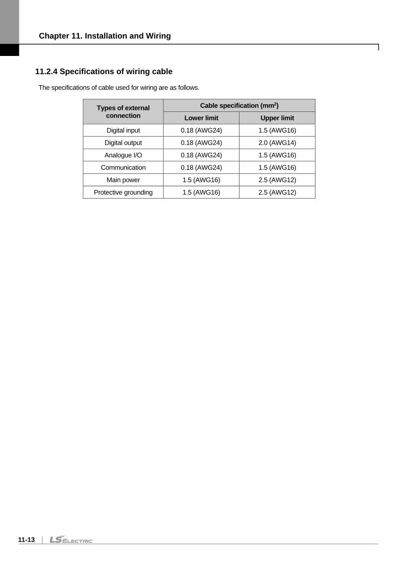
Chapter 11. Installation and Wiring
11-13
11.2.4 Specifications of wiring cable The specifications of cable used for wiring are as follows.
Types of external connection
Cable specification (mm2)
Lower limit Upper limit
Digital input 0.18 (AWG24) 1.5 (AWG16)
Digital output 0.18 (AWG24) 2.0 (AWG14)
Analogue I/O 0.18 (AWG24) 1.5 (AWG16)
Communication 0.18 (AWG24) 1.5 (AWG16)
Main power 1.5 (AWG16) 2.5 (AWG12)
Protective grounding 1.5 (AWG16) 2.5 (AWG12)

Chapter 11. Installation and Wiring
11-14
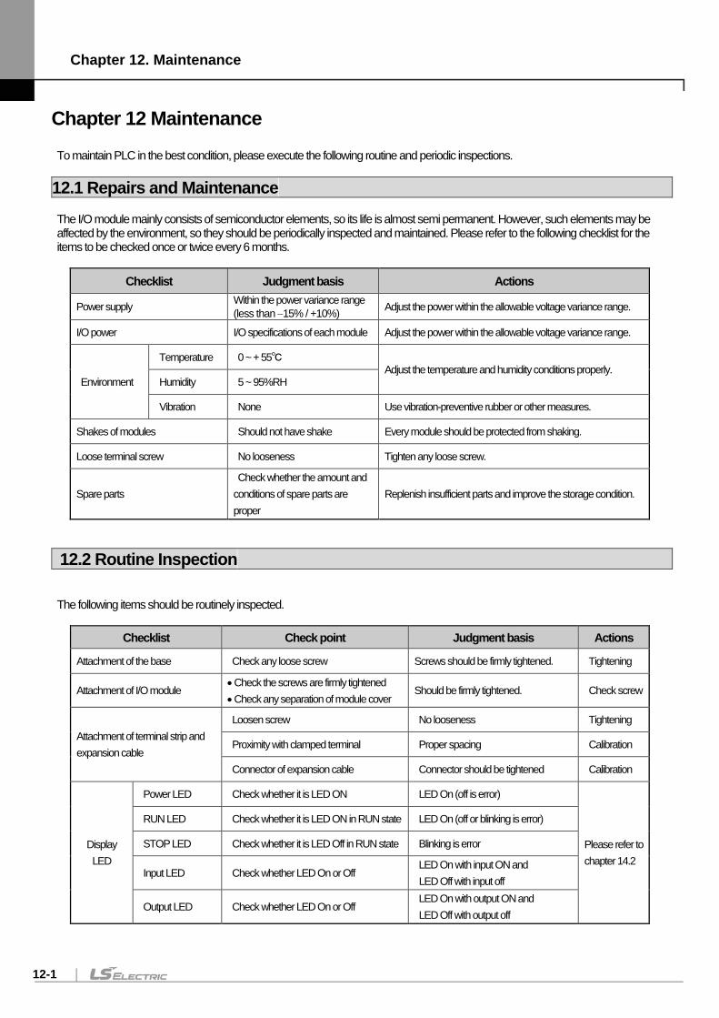
Chapter 12. Maintenance
12-1
Chapter 12 Maintenance To maintain PLC in the best condition, please execute the following routine and periodic inspections.
12.1 Repairs and Maintenance The I/O module mainly consists of semiconductor elements, so its life is almost semi permanent. However, such elements may be affected by the environment, so they should be periodically inspected and maintained. Please refer to the following checklist for the items to be checked once or twice every 6 months.
Checklist Judgment basis Actions
Power supply Within the power variance range (less than −15% / +10%) Adjust the power within the allowable voltage variance range.
I/O power I/O specifications of each module Adjust the power within the allowable voltage variance range.
Environment
Temperature 0 ~ + 55 Adjust the temperature and humidity conditions properly.
Humidity 5 ~ 95%RH
Vibration None Use vibration-preventive rubber or other measures.
Shakes of modules Should not have shake Every module should be protected from shaking.
Loose terminal screw No looseness Tighten any loose screw.
Spare parts Check whether the amount and conditions of spare parts are proper
Replenish insufficient parts and improve the storage condition.
12.2 Routine Inspection The following items should be routinely inspected.
Checklist Check point Judgment basis Actions
Attachment of the base Check any loose screw Screws should be firmly tightened. Tightening
Attachment of I/O module • Check the screws are firmly tightened • Check any separation of module cover
Should be firmly tightened. Check screw
Attachment of terminal strip and expansion cable
Loosen screw No looseness Tightening
Proximity with clamped terminal Proper spacing Calibration
Connector of expansion cable Connector should be tightened Calibration
Display LED
Power LED Check whether it is LED ON LED On (off is error)
Please refer to chapter 14.2
RUN LED Check whether it is LED ON in RUN state LED On (off or blinking is error)
STOP LED Check whether it is LED Off in RUN state Blinking is error
Input LED Check whether LED On or Off LED On with input ON and LED Off with input off
Output LED Check whether LED On or Off LED On with output ON and LED Off with output off
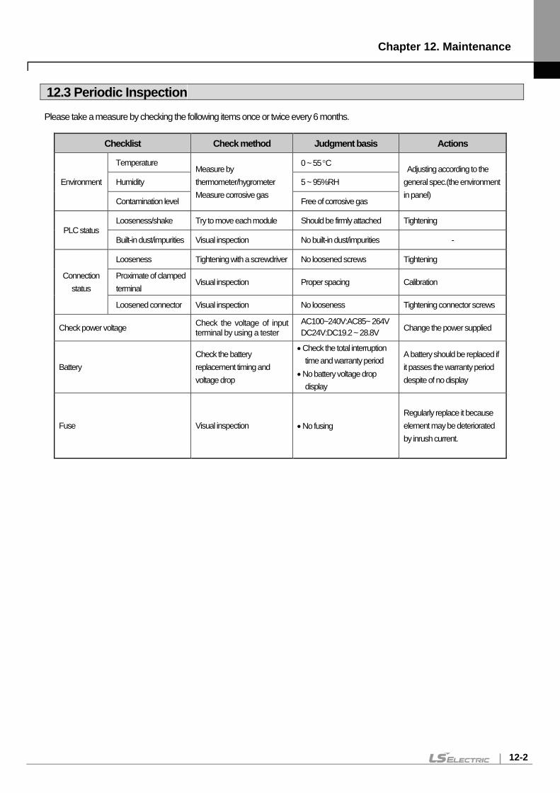
Chapter 12. Maintenance
12-2
12.3 Periodic Inspection Please take a measure by checking the following items once or twice every 6 months.
Checklist Check method Judgment basis Actions
Environment
Temperature Measure by thermometer/hygrometer Measure corrosive gas
0 ~ 55 °C Adjusting according to the general spec.(the environment in panel)
Humidity 5 ~ 95%RH
Contamination level Free of corrosive gas
PLC status Looseness/shake Try to move each module Should be firmly attached Tightening
Built-in dust/impurities Visual inspection No built-in dust/impurities -
Connection status
Looseness Tightening with a screwdriver No loosened screws Tightening
Proximate of clamped terminal
Visual inspection Proper spacing Calibration
Loosened connector Visual inspection No looseness Tightening connector screws
Check power voltage Check the voltage of input terminal by using a tester
AC100~240V:AC85~ 264V DC24V:DC19.2 ~ 28.8V Change the power supplied
Battery Check the battery replacement timing and voltage drop
• Check the total interruption time and warranty period
• No battery voltage drop display
A battery should be replaced if it passes the warranty period despite of no display
Fuse Visual inspection • No fusing
Regularly replace it because element may be deteriorated by inrush current.
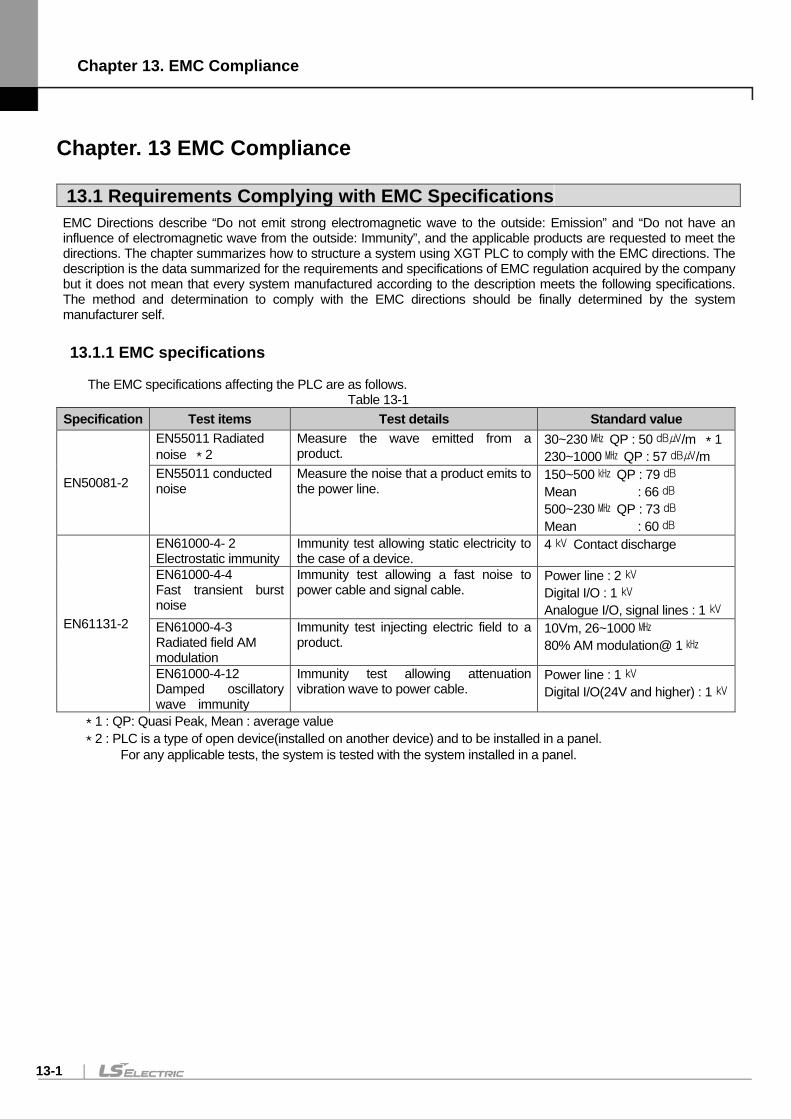
Chapter 13. EMC Compliance
13-1
Chapter. 13 EMC Compliance
13.1 Requirements Complying with EMC Specifications EMC Directions describe “Do not emit strong electromagnetic wave to the outside: Emission” and “Do not have an influence of electromagnetic wave from the outside: Immunity”, and the applicable products are requested to meet the directions. The chapter summarizes how to structure a system using XGT PLC to comply with the EMC directions. The description is the data summarized for the requirements and specifications of EMC regulation acquired by the company but it does not mean that every system manufactured according to the description meets the following specifications. The method and determination to comply with the EMC directions should be finally determined by the system manufacturer self.
13.1.1 EMC specifications The EMC specifications affecting the PLC are as follows.
Table 13-1 Specification Test items Test details Standard value
EN50081-2
EN55011 Radiated noise *2
Measure the wave emitted from a product.
30~230 QP : 50/m *1 230~1000 QP : 57/m
EN55011 conducted noise
Measure the noise that a product emits to the power line.
150~500 QP : 79 Mean : 66 500~230 QP : 73 Mean : 60
EN61131-2
EN61000-4- 2 Electrostatic immunity
Immunity test allowing static electricity to the case of a device.
4 Contact discharge
EN61000-4-4 Fast transient burst noise
Immunity test allowing a fast noise to power cable and signal cable.
Power line : 2 Digital I/O : 1 Analogue I/O, signal lines : 1
EN61000-4-3 Radiated field AM modulation
Immunity test injecting electric field to a product.
10Vm, 26~1000 80% AM modulation@ 1
EN61000-4-12 Damped oscillatory wave immunity
Immunity test allowing attenuation vibration wave to power cable.
Power line : 1 Digital I/O(24V and higher) : 1
*1 : QP: Quasi Peak, Mean : average value *2 : PLC is a type of open device(installed on another device) and to be installed in a panel.
For any applicable tests, the system is tested with the system installed in a panel.
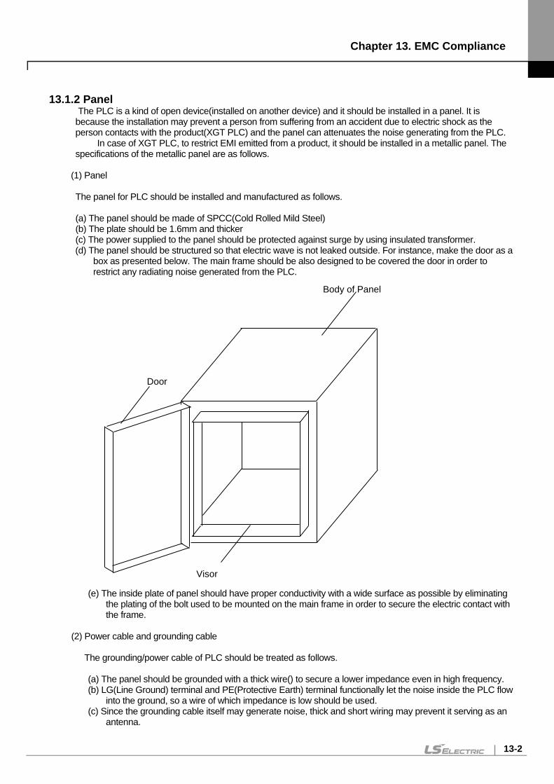
Chapter 13. EMC Compliance
13-2
13.1.2 Panel The PLC is a kind of open device(installed on another device) and it should be installed in a panel. It is
because the installation may prevent a person from suffering from an accident due to electric shock as the person contacts with the product(XGT PLC) and the panel can attenuates the noise generating from the PLC.
In case of XGT PLC, to restrict EMI emitted from a product, it should be installed in a metallic panel. The specifications of the metallic panel are as follows.
(1) Panel The panel for PLC should be installed and manufactured as follows.
(a) The panel should be made of SPCC(Cold Rolled Mild Steel) (b) The plate should be 1.6mm and thicker (c) The power supplied to the panel should be protected against surge by using insulated transformer. (d) The panel should be structured so that electric wave is not leaked outside. For instance, make the door as a
box as presented below. The main frame should be also designed to be covered the door in order to restrict any radiating noise generated from the PLC.
(e) The inside plate of panel should have proper conductivity with a wide surface as possible by eliminating
the plating of the bolt used to be mounted on the main frame in order to secure the electric contact with the frame.
(2) Power cable and grounding cable
The grounding/power cable of PLC should be treated as follows. (a) The panel should be grounded with a thick wire() to secure a lower impedance even in high frequency. (b) LG(Line Ground) terminal and PE(Protective Earth) terminal functionally let the noise inside the PLC flow
into the ground, so a wire of which impedance is low should be used. (c) Since the grounding cable itself may generate noise, thick and short wiring may prevent it serving as an
antenna.
Body of Panel
Door
Visor
Chapter 13. EMC Compliance
13-3
13.1.3 Cable (1) Expansion cables can be classified into optical and electrical cables according to the connector type.
(a) For the optical cables, use MMF(Multi Mode Fiber) 50/65um LC Type Cable. Use indoor type, outdoor type, or conduit type according to the installation site.
Fig. MMF(LC Type) cable
(b) For the electrical cables, communication can be done with 100Mbit Twisted Pair cables, however, since the data transmission in expansion cables is in tens of micro unit, external noise may affect system performance and control seriously.
Therefore, electrical cables used in XGR systems should, basically, be shielded twisted pair cables such as FTP, STP, or FSTP.
Fig. FTP Cable
Fig. STP Cable
(2) Fixing a cable in the panel
If the expansion cable of XGT series is to be installed on the metallic panel, the cable should be 1cm and more away from the panel, preventing the direct contact. The metallic plate of panel may shield noise from electromagnetic wave while it a cable as a noise source is close to the place, it can serve as an antenna. Every fast signal cable as well as the expansion cable needs proper spacing from the panel
Chapter 13. EMC Compliance
13-4
13.2 Requirements Complying with Low Voltage Direction The low voltage direction requires a device that operates with AC50~1000V, DC 75 ~ 1500V to have proper safety. The followings summarize the cautions for installing and wiring PLC of the XGT series to comply with the low voltage directions. The description is the data based on the applicable requirements and specifications as far as we know but it does not mean that every system manufactured according to the description meets the following specifications. The method and determination to comply with the EMC directions should be finally determined by the system manufacturer self.
13.2.1 Specifications applicable to XGT series XGT series follow the EN6100-1(safety of the device used in measurement/control lab). XGT series is developed in accordance with the above specifications, even for a module operating at the rated voltage higher than AC50V/DC75V.
13.2.2 Selection of XGT series PLC (1) Power module
The power module of which rated input voltage is AC110/220V may have dangerous voltage(higher than 42.4V peak) inside it, so any CE mark compliance product is insulated between the primary and the secondary.
(2) I/O module
The I/O module of which rated voltage is AC110/220V may have dangerous voltage(higher than 42.4V peak) inside it, so any CE mark compliance product is insulated between the primary and the secondary. The I/O module lower than DC24V is not applicable to the low voltage directions.
(3) CPU Module, Base unit The modules use DC5V, 3.3V circuits, so they are not applicable to the low voltage directions.
(4) Special module, Communication module The modules use the rated voltage less than DC 24V, so they are not applicable to the low voltage directions.
Chapter 14. Built-in PID Function
14-1
Chapter 14 Built-in PID Function This chapter describes XGR Series CPU built-in PID function.
14.1 Features The features of PID function built-in XGR-CPU are as follows. (1) It can execute precise control operation. (2) It has a fast operation cycle up to 0.6ms. (3) XGR CPUH can operate totally 256 loops by using 32 loops in 8 blocks. (4) Symbol variable function facilitates setting and monitoring. (5) It supports forward/reverse operation process. (6) Strong dual anti windup prevents effective over/under shoot. (7) It may be operated by external device (HMI). (8) It protects the system by restricting the max. variance of PV. (9) It protects the drive by restricting the max. variance, max value and min value of MV. (10) Auto-tuning function is used for PID control. (11) Cascade PID control is available.
14.2 PID Control PID Control compares the value measured at detection (process value) to the pre-determined value, adjusts outputs (control signal) to eliminate, if any, an error between two values, making the current value to the target value, in order to maintain the state of an object to control be a pre-determined value (target value).
User SV
PID operation
CPU module
SenseAD
Conversion module
DAConversion
module
Objectcontrol
PV
User
Auto
Manual
MV_manual
MVMV Dri
ver
As presented in the above figure, PLC functions as a control in a whole control system while sensor and driver are used to detect an object to control and drive the system, respectively. When a sensor detects the current state of an object to control and delivers it to a control, PLC executes an operation of output and delivers it to a driver. Meanwhile, a driver drives the object according to the output. Finally, a sensor detects the changed state and re-sends it to PLC, forming a closed loop. A procedure circulating a control loop repeats at the unit of several seconds and hundreds of microseconds and the time is called control cycle.
Chapter 14. Built-in PID Function
14-2
14.3 PID Control Operation
14.3.1 Terms used It describes the terms necessary to explain PID control operation.
SV : Set value to which an object to control should reach T_s(Ts) : Sampling time (control cycle) K_p(Kp) : Proportional constant T_i(Ti) : Integral time constant T_d(Td) : Differential time constant PV : Current state of an object to control, which is detected by a sensor E : Error of an object to control, which is expressed in (SV – PV) MV : Control input or control’s output MV_p(MVp) : Proportional component of MV MV_i(MVi) : Integral component of MV MV_d(MVd) : Differential component of MV
14.3.2 PID equation PID Equation may be expressed from equation (14.3.1) through equation (14.3.5).
)5.3.14(
)4.3.14(
)3.3.14(
)2.3.14(
)1.3.14(
dip
dpd
i
pi
pp
MVMVMVMV
dtdETKMV
dtETK
MV
EKMV
PVSVE
++=
=
=
=
−=
∫
Error is a mathematical expression indicating how far the current system is out of a user’s desirable state. For instance, assuming that a user wishes to maintain water in an electric kettle at 50 and the temperature of water is 35, SV and PV are 50 and 35, respectively and error E is 15, the difference between SV and PV. The control executes PID operation according to the error. Note that MV totally consists of each component of P, I and D, that is, MV_p, MV_i and MV_d, as presented in figure (14.3.5). namely, if subtracting D from PID control equation, it results in PI control; alike, if subtracting I and D, it results in P control.
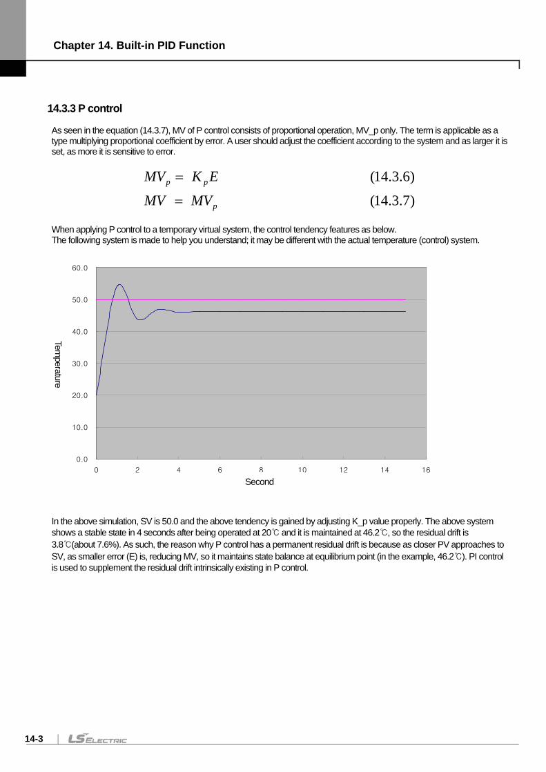
Chapter 14. Built-in PID Function
14-3
14.3.3 P control As seen in the equation (14.3.7), MV of P control consists of proportional operation, MV_p only. The term is applicable as a type multiplying proportional coefficient by error. A user should adjust the coefficient according to the system and as larger it is set, as more it is sensitive to error.
)7.3.14()6.3.14(
p
pp
MVMVEKMV
=
=
When applying P control to a temporary virtual system, the control tendency features as below. The following system is made to help you understand; it may be different with the actual temperature (control) system.
0.0
10.0
20.0
30.0
40.0
50.0
60.0
0 2 4 6 8 10 12 14 16
초
온도
In the above simulation, SV is 50.0 and the above tendency is gained by adjusting K_p value properly. The above system shows a stable state in 4 seconds after being operated at 20 and it is maintained at 46.2, so the residual drift is 3.8(about 7.6%). As such, the reason why P control has a permanent residual drift is because as closer PV approaches to SV, as smaller error (E) is, reducing MV, so it maintains state balance at equilibrium point (in the example, 46.2). PI control is used to supplement the residual drift intrinsically existing in P control.
Second Tem
perature
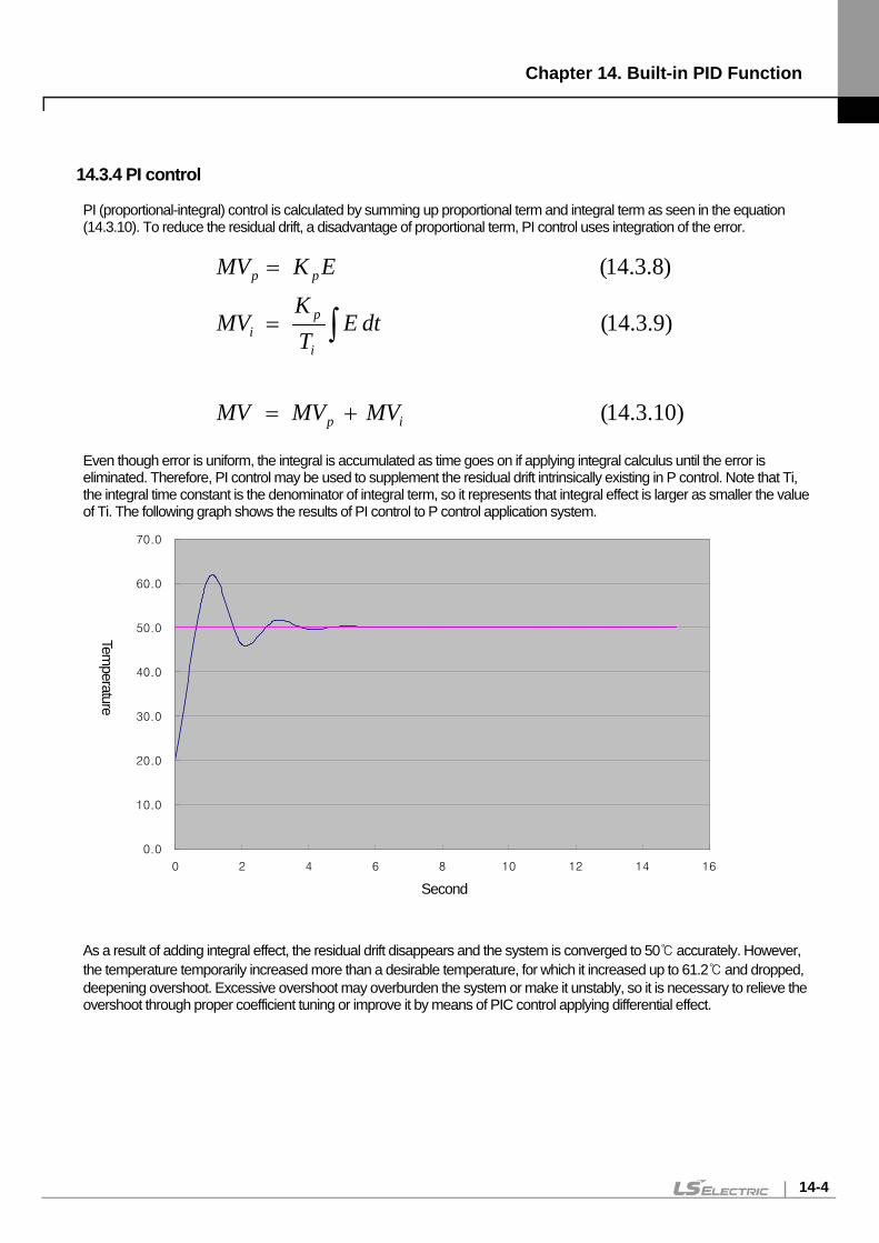
Chapter 14. Built-in PID Function
14-4
14.3.4 PI control PI (proportional-integral) control is calculated by summing up proportional term and integral term as seen in the equation (14.3.10). To reduce the residual drift, a disadvantage of proportional term, PI control uses integration of the error.
)10.3.14(
)9.3.14(
)8.3.14(
ip
i
pi
pp
MVMVMV
dtETK
MV
EKMV
+=
=
=
∫
Even though error is uniform, the integral is accumulated as time goes on if applying integral calculus until the error is eliminated. Therefore, PI control may be used to supplement the residual drift intrinsically existing in P control. Note that Ti, the integral time constant is the denominator of integral term, so it represents that integral effect is larger as smaller the value of Ti. The following graph shows the results of PI control to P control application system.
0.0
10.0
20.0
30.0
40.0
50.0
60.0
70.0
0 2 4 6 8 10 12 14 16
초
온도
As a result of adding integral effect, the residual drift disappears and the system is converged to 50 accurately. However, the temperature temporarily increased more than a desirable temperature, for which it increased up to 61.2 and dropped, deepening overshoot. Excessive overshoot may overburden the system or make it unstably, so it is necessary to relieve the overshoot through proper coefficient tuning or improve it by means of PIC control applying differential effect.
Second
Temperature
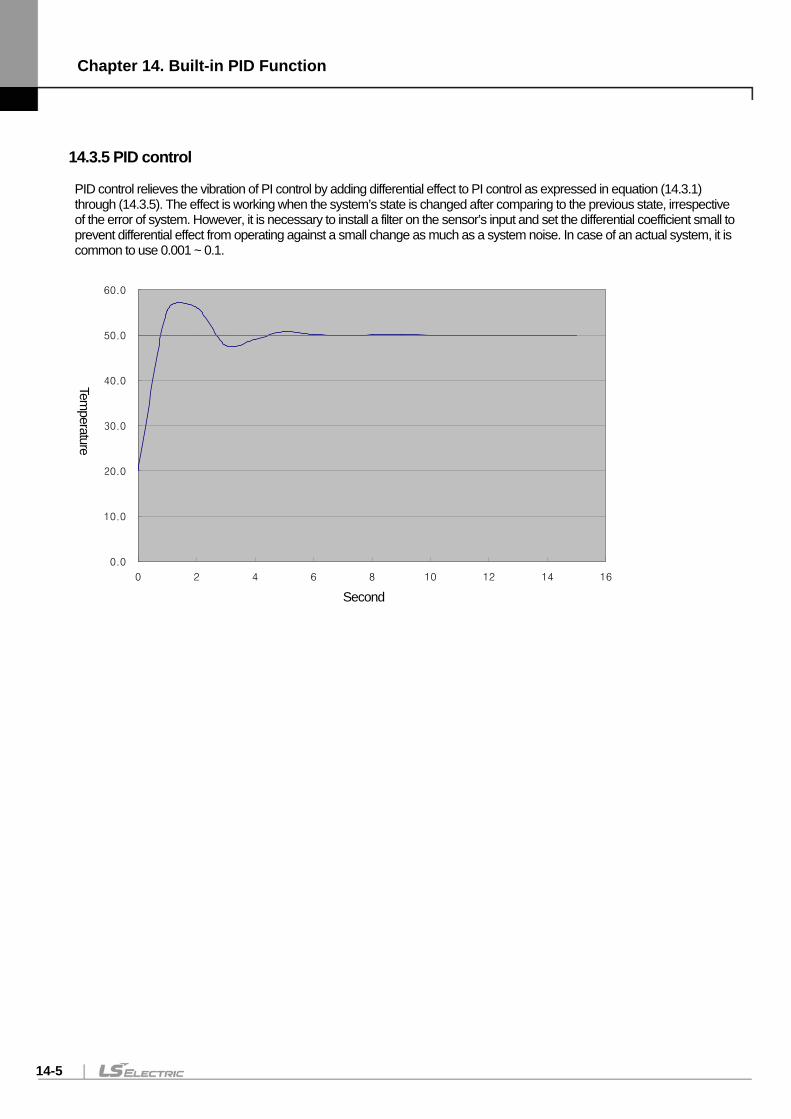
Chapter 14. Built-in PID Function
14-5
14.3.5 PID control PID control relieves the vibration of PI control by adding differential effect to PI control as expressed in equation (14.3.1) through (14.3.5). The effect is working when the system’s state is changed after comparing to the previous state, irrespective of the error of system. However, it is necessary to install a filter on the sensor’s input and set the differential coefficient small to prevent differential effect from operating against a small change as much as a system noise. In case of an actual system, it is common to use 0.001 ~ 0.1.
0.0
10.0
20.0
30.0
40.0
50.0
60.0
0 2 4 6 8 10 12 14 16
초
온도
Second
Temperature
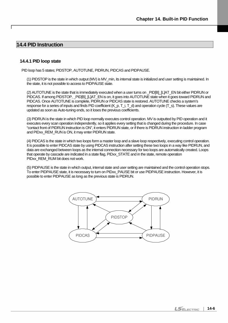
Chapter 14. Built-in PID Function
14-6
14.4 PID Instruction
14.4.1 PID loop state PID loop has 5 states; PIDSTOP, AUTOTUNE, PIDRUN, PIDCAS and PIDPAUSE.
(1) PIDSTOP is the state in which output (MV) is MV_min, its internal state is initialized and user setting is maintained. In the state, it is not possible to access to PIDPAUSE state. (2) AUTOTUNE is the state that is immediately executed when a user turns on _PID[B]_[L]AT_EN bit either PIDRUN or PIDCAS. If among PIDSTOP, _PID[B]_[L]AT_EN is on, it goes into AUTOTUNE state when it goes toward PIDRUN and PIDCAS. Once AUTOTUNE is complete, PIDRUN or PIDCAS state is restored. AUTOTUNE checks a system’s response for a series of inputs and finds PID coefficient (K_p, T_i, T_d) and operation cycle (T_s). These values are updated as soon as Auto-tuning ends, so it loses the previous coefficients. (3) PIDRUN is the state in which PID loop normally executes control operation. MV is outputted by PID operation and it executes every scan operation independently, so it applies every setting that is changed during the procedure. In case “contact front of PIDRUN instruction is ON”, it enters PIDRUN state, or if there is PIDRUN instruction in ladder program and PIDxx_REM_RUN is ON, it may enter PIDRUN state. (4) PIDCAS is the state in which two loops form a master loop and a slave loop respectively, executing control operation. It is possible to enter PIDCAS state by using PIDCAS instruction after setting these two loops in a way like PIDRUN, and data are exchanged between loops as the internal connection necessary for two loops are automatically created. Loops that operate by cascade are indicated in a state flag, PIDxx_STATE and in the state, remote operation PIDxx_REM_RUM bit does not work. (5) PIDPAUSE is the state in which output, internal state and user setting are maintained and the control operation stops. To enter PIDPAUSE state, it is necessary to turn on PIDxx_PAUSE bit or use PIDPAUSE instruction. However, it is possible to enter PIDPAUSE as long as the previous state is PIDRUN.
PIDRUN
PIDPAUSE
PIDSTOP
PIDCAS
AUTOTUNE
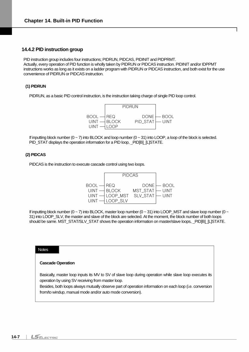
Chapter 14. Built-in PID Function
14-7
14.4.2 PID instruction group PID instruction group includes four instructions; PIDRUN, PIDCAS, PIDINIT and PIDPRMT. Actually, every operation of PID function is wholly taken by PIDRUN or PIDCAS instruction. PIDINIT and/or IDPPMT instructions works as long as it exists on a ladder program with PIDRUN or PIDCAS instruction, and both exist for the use convenience of PIDRUN or PIDCAS instruction.
(1) PIDRUN
PIDRUN, as a basic PID control instruction, is the instruction taking charge of single PID loop control.
PIDRUN
PID_STAT UINTDONE BOOL
BLOCKUINTREQBOOL
LOOPUINT If inputting block number (0 ~ 7) into BLOCK and loop number (0 ~ 31) into LOOP, a loop of the block is selected. PID_STAT displays the operation information for a PID loop, _PID[B]_[L]STATE.
(2) PIDCAS
PIDCAS is the instruction to execute cascade control using two loops.
PIDCAS
REQBOOL DONE BOOLMST_STAT UINTSLV_STAT UINT
LOOP_SLVUINTLOOP_MSTUINTBLOCKUINT
If inputting block number (0 ~ 7) into BLOCK, master loop number (0 ~ 31) into LOOP_MST and slave loop number (0 ~ 31) into LOOP_SLV, the master and slave of the block are selected. At the moment, the block number of both loops should be same. MST_STAT/SLV_STAT shows the operation information on master/slave loops, _PID[B]_[L]STATE.
Notes
Cascade Operation Basically, master loop inputs its MV to SV of slave loop during operation while slave loop executes its operation by using SV receiving from master loop. Besides, both loops always mutually observe part of operation information on each loop (i.e. conversion from/to windup, manual mode and/or auto mode conversion).
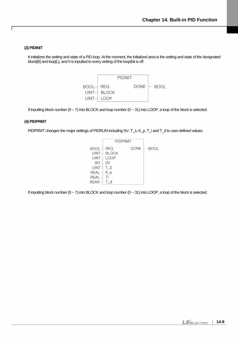
Chapter 14. Built-in PID Function
14-8
(3) PIDINIT
It initializes the setting and state of a PID loop. At the moment, the initialized area is the setting and state of the designated block[B] and loop[L], and 0 is inputted to every setting of the loop(bit is off.
PIDINIT
DONE BOOLREQBOOL
LOOPUINT
BLOCKUINT
If inputting block number (0 ~ 7) into BLOCK and loop number (0 ~ 31) into LOOP, a loop of the block is selected.
(4) PIDPRMT PIDPRMT changes the major settings of PIDRUN including SV, T_s, K_p, T_i and T_d to user-defined values.
PIDPRMT
DONE BOOLREQBOOL
SVINT
LOOPUINT
T_SUINT
TiREAL
K_pREAL
T_dREAR
BLOCKUINT
If inputting block number (0 ~ 7) into BLOCK and loop number (0 ~ 31) into LOOP, a loop of the block is selected.
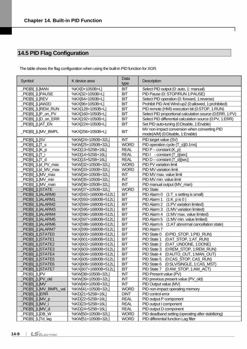
Chapter 14. Built-in PID Function
14-9
14.5 PID Flag Configuration The table shows the flag configuration when using the built-in PID function for XGR.
Symbol K device area Data type Description
_PID[B]_[L]MAN %KX[0+1050B+L] BIT Select PID output (0: auto, 1: manual) _PID[B]_[L]PAUSE %KX[32+1050B+L] BIT PID Pause (0: STOP/RUN 1:PAUSE) _PID[B]_[L]REV %KX[64+1050B+L] BIT Select PID operation (0: forward, 1:reverse) _PID[B]_[L]AW2D %KX[96+1050B+L] BIT Prohibit PID Anti Wind-up2 (0:allowed, 1:prohibited) _PID[B]_[L]REM_RUN %KX[128+1050B+L] BIT PID remote (HMI) execution bit (0:STOP, 1:RUN) _PID[B]_[L]P_on_PV %KX[160+1050B+L] BIT Select PID proportional calculation source (0:ERR, 1:PV) _PID[B]_[L]D_on_ERR %KX[192+1050B+L] BIT Select PID differential calculation source (0:PV, 1:ERR) _PID[B]_[L]AT_EN %KX[224+1050B+L] BIT Set PID auto-tuning (0:Disable, 1:Enable)
_PID[B]_[L]MV_BMPL %KX[256+1050B+L] BIT MV non-impact conversion when converting PID mode(A/M) (0:Disable, 1:Enable)
_PID[B]_[L]SV %KW[24+1050B+32L] INT PID target value (SV) _PID[B]_[L]T_s %KW[25+1050B+32L] WORD PID operation cycle (T_s)[0.1ms] _PID[B]_[L]K_p %KD[13+525B+16L] REAL PID P – constant (K_p) _PID[B]_[L]T_i %KD[14+525B+16L] REAL PID I - constant (T_i)[sec] _PID[B]_[L]T_d %KD[15+525B+16L] REAL PID D – constant (T_d)[sec] _PID[B]_[L]d_PV_max %KW[32+1050B+32L] WORD PID PV variation limit _PID[B]_[L]d_MV_max %KW[33+1050B+32L] WORD PID MV variation limit _PID[B]_[L]MV_max %KW[34+1050B+32L] INT PID MV max. value limit _PID[B]_[L]MV_min %KW[35+1050B+32L] INT PID MV min. value limit _PID[B]_[L]MV_man %KW[36+1050B+32L] INT PID manual output (MV_man) _PID[B]_[L]STATE %KW[37+1050B+32L] WORD PID State _PID[B]_[L]ALARM0 %KX[592+16800B+512L] BIT PID Alarm 0 (1:T_s setting is small) _PID[B]_[L]ALARM1 %KX[593+16800B+512L] BIT PID Alarm 1 (1:K_p is 0 ) _PID[B]_[L]ALARM2 %KX[594+16800B+512L] BIT PID Alarm 2 (1:PV variation limited) _PID[B]_[L]ALARM3 %KX[595+16800B+512L] BIT PID Alarm 3 (1:MV variation limited) _PID[B]_[L]ALARM4 %KX[596+16800B+512L] BIT PID Alarm 4 (1:MV max. value limited) _PID[B]_[L]ALARM5 %KX[597+16800B+512L] BIT PID Alarm 5 (1:MV min. value limited) _PID[B]_[L]ALARM6 %KX[598+16800B+512L] BIT PID Alarm 6 (1:AT abnormal cancellation state) _PID[B]_[L]ALARM7 %KX[599+16800B+512L] BIT PID Alarm 7 _PID[B]_[L]STATE0 %KX[600+16800B+512L] BIT PID State 0 (0:PID_STOP, 1:PID_RUN) _PID[B]_[L]STATE1 %KX[601+16800B+512L] BIT PID State 1 (0:AT_STOP, 1:AT_RUN) _PID[B]_[L]STATE2 %KX[602+16800B+512L] BIT PID State 2 (0:AT_UNDONE, 1:DONE) _PID[B]_[L]STATE3 %KX[603+16800B+512L] BIT PID State 3 (0:REM_STOP, 1:REM_RUN) _PID[B]_[L]STATE4 %KX[604+16800B+512L] BIT PID State 4 (0:AUTO_OUT, 1:MAN_OUT) _PID[B]_[L]STATE5 %KX[605+16800B+512L] BIT PID State 5 (0:CAS_STOP, CAS_RUN) _PID[B]_[L]STATE6 %KX[606+16800B+512L] BIT PID State 6 (0:SLV/SINGLE, 1:CAS_MST) _PID[B]_[L]STATE7 %KX[607+16800B+512L] BIT PID State 7 (0:AW_STOP, 1:AW_ACT) _PID[B]_[L]PV %KW[38+1050B+32L] INT PID Present value (PV) _PID[B]_[L]PV_old %KW[39+1050B+32L] INT PID previous present value (PV_old) _PID[B]_[L]MV %KW[40+1050B+32L] INT PID Output value (MV) _PID[B]_[L]MV_BMPL_val %KW[41+1050B+32L] WORD PID non-impact operating memory _PID[B]_[L]ERR %KD[21+525B+16L] DINT PID control error _PID[B]_[L]MV_p %KD[22+525B+16L] REAL PID output P component _PID[B]_[L]MV_i %KD[23+525B+16L] REAL PID output I component _PID[B]_[L]MV_d %KD[24+525B+16L] REAL PID output D component _PID[B]_[L]DB_W %KW[50+1050B+32L] WORD PID deadband setting (operating after stabilizing) _PID[B]_[L]Td_lag %KW[51+1050B+32L] WORD PID differential function Lag filter
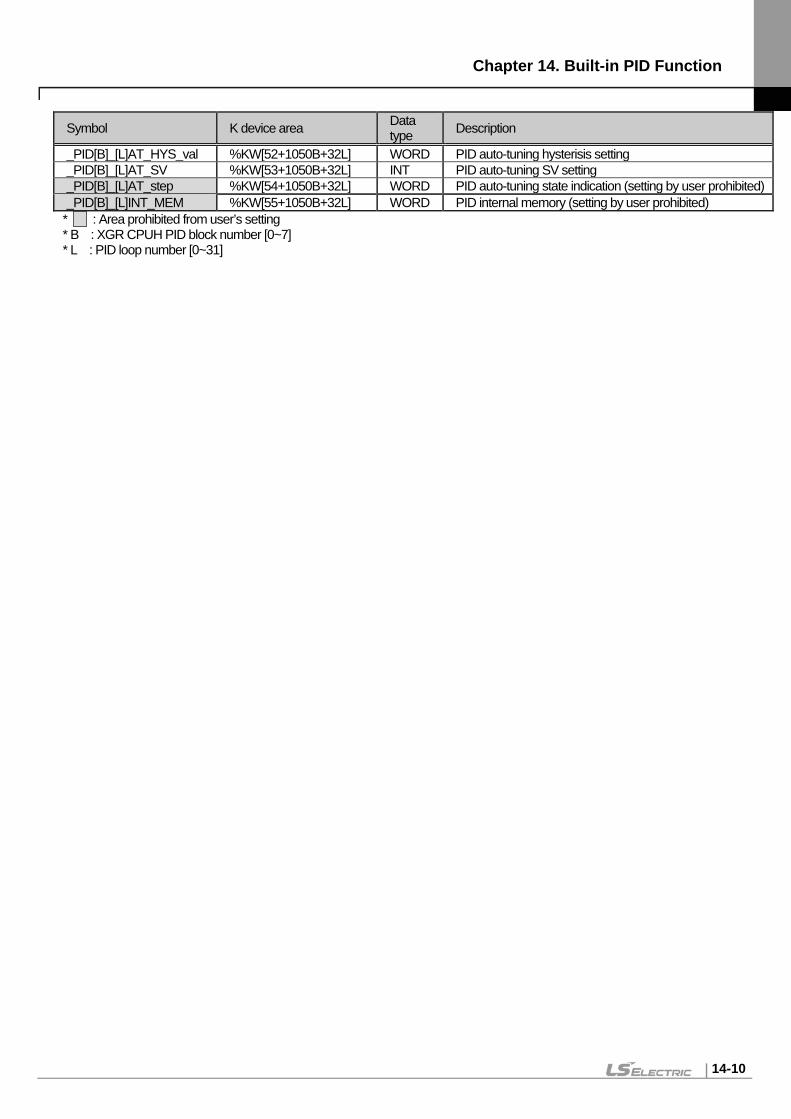
Chapter 14. Built-in PID Function
14-10
Symbol K device area Data type Description
_PID[B]_[L]AT_HYS_val %KW[52+1050B+32L] WORD PID auto-tuning hysterisis setting _PID[B]_[L]AT_SV %KW[53+1050B+32L] INT PID auto-tuning SV setting _PID[B]_[L]AT_step %KW[54+1050B+32L] WORD PID auto-tuning state indication (setting by user prohibited) _PID[B]_[L]INT_MEM %KW[55+1050B+32L] WORD PID internal memory (setting by user prohibited)
* : Area prohibited from user’s setting * B : XGR CPUH PID block number [0~7] * L : PID loop number [0~31]
Chapter 14. Built-in PID Function
14-11
%KX[0+1050B] ~ %KX[287+1050B] area is the common bit area of the block PID loop. The bit state and settings of each bit are collected and arranged on the front of each PID block. Therefore, 32 bits, the max. no. of loops that PID function may use in a block is collected, forming a double-word, and the state and setting of each bit are saved in good order of bits. %KW0024 ~ %KW0055 area is the individual data area for PID block 0 and loop 0, where the setting and state of block 0 and loop 0 are saved. The loop setting for the PID loop such as SV, dPV_max, MV_man, T_s, Kp, Ti, Td, MV_max, MV_min and dMV_max are saved in the area, and during the execution of PID function, the state of PID loops such as PV, ETC, MV, MV_rvs, ERR, MVp, MVi, MVd and PV are also saved. A user may change PID setting simply by writing data on the memory and get the result reflected to the next cycle. %KW0056 ~ %KW1047 area is the memory of loop 1 through 31 with the format of block 0 & loop 0. Each loop independently works and may execute auxiliary operation like the application of cascade. Additionally, the K device memory configuration mentioned in the end of user’s manual may help you understand the memory location of PID. The location and order of the memory area as mentioned above may change without prior notice to improve the product performance.
Notes
1) PID memory statement format _PID[B]_[L]MAN B: block, L : loop i.e.) _PID3_05MAN : means MAN bit of block 3 and loop 5.
2) Common bit area
i.e.) _PID3_25PAUSE : because of block 3 and loop 25, it represents the location of %KX[32+1050B+L] = %KX3207.
3) Individual data area
i.e.) _PID5_30SV : because of block 5 and loop 30, it represents the location of %KW[24+1050B+32L] = %KW6234.
Chapter 14. Built-in PID Function
14-12
14.5.1 Common bit area Common bit area is the part that gathers every data consisting of bits for each of 32 loops. It has a double word format of 32 bits as the information on 32 loops for an item; n th bit means the information on the n th loop. m is the value that the loop number, n is converted to a hexadecimal.
(1) _PID[B]_[L]MAN (PID Manual operation enable) - Setting area K DEVICE AREA : %KX [0+1050B+L] Data unit : BIT It determines whether PID function of n th loop is operated manually or automatically(AUTO/MANUAL). AUTO state outputs the results that PID operation is normally executed while MANUAL state does not execute PID operation and instead, it outputs a use desirable temporary value. At the moment, the output is generated as _PID[B]_[L]MV_man, which is the value a user wishes. If a bit is off, it is set as [Default] AUTO.
(2) _PID[B]_[L]PAUSE (PID PAUSE mode) - Setting area K DEVICE AREA : %KX [32+1050B+L] Data unit : BIT It makes n th PID loop in pause state. If converting PAUSE to RUN state again, it continuously controls. Therefore, since control system may result in unexpected results if the system state is changed in PAUSE, PAUSE function should be carefully used. If the bit is off, [Default] PAUSE is cancelled.
(3) _PID[B]_[L]REV (PID REVerse operation) - Setting area K DEVICE AREA : %KX64+1050B+L] Data unit : BIT It sets whether a control system is forward system or reverse system. If system state ascends when system input rises, it is called forward system; if it descends when it increases, it is called reverse system. In case of boiler, the temperature rises as the system input increases, so it is a forward system. On the other hand, in case of cooling system, the temperature drops as the system input rises, so it is a reverse system. If the bit is off, it is set as [Default] Forward system.
Notes
_PID[B]_[L]PAUSE If making PID loop in PAUSE state by using PID[B]_[L]PAUSE and PIDPAUSE instruction, every operation stops and it outputs the last calculation before PAUSE state. In the case, if system state is changed, the control system may show unexpected results due to improper control, so PAUSE function should be carefully used. In the first scan of PLC, since PIDRUN instruction executes initialization, in which PAUSE bit is off, it escapes from PAUSE and turns STOP or RUN state if turning on PLC in PAUSE state.
Chapter 14. Built-in PID Function
14-13
(4) _PID[B]_[L]AW2D (PID Anti Wind-up 2 Disable) - Setting area K DEVICE AREA : %KX[96+1050B+L] Data unit : BIT If the bit is off when a user does not want it, Anti Wind-up2 function is deactivated. The function of Anti wind-up is detailed in 14.6. If the bit is off, [Default] Anti Wind-up2 function is enabled.
(5) _PID[B]_[L]REM_RUN (PID REMote RUN) - Setting area K DEVICE AREA : %KX[128+1050B+L] Data unit : BIT It is the external operation instruction of PIDRUN. Being used as an external operation instruction, it functions alike the effect that PIDRUN instruction contact is on/off. Indeed, PIDRUN instruction executes OR operation of “PIDRUN instruction’s input condition” contact and the bit to determine whether to execute the operation. If using the function, PIDRUN instruction’s operation contact may be assigned to a fixed address, so a user may conveniently use external I/O devices such as HMI. If the bit is off, [Default] (if contact is off), PIDRUN instruction stops.
(6) _PID[B]_[L]P_on_PV (PID P on PV) - Setting area K DEVICE AREA: %KX[160+1050B+L] Data unit : BIT It sets the P operation source of PID loop as PV. P operation is operated with ERR or PV, and P operation using PV is relatively slow moving to stable state, rather using ERR, in an unstable state of instantaneous control due to initial response or disturbance. It means that output fluctuation is not steep and consequently, it does not overburden the driver. However, since the range of internal operation value changes, Anti Wind-up function does not work. If the bit is off, PID executes P operation with ERR in [Default] state and in case of on, it executes P operation with PV value.
(7) _PID[B]_[L]D_on_ERR (PID D on ERRor) - Setting area K DEVICE AREA : %KX[192+1050B+L] Data unit : BIT It sets the D operation source of PID loop as ERR. D operation is operated with ERR or PV, and D operation using ERR may cause excessive input to a driver instantly because D response may have sudden change as SV is changed by a user. To prevent it, D operation uses PV and the default is also set to be D operation using PV. If using ERR without the algorithm, the bit should be on. If the bit is off, PID executes D operation with PV in [Default] state, and in ON state, it executes D operation with ERR value. Notes
_PID[B]_[L]REM_RUN The bit is saved in K device even though PLC stops, so if PLC stops and operates with the bit ON (i.e. power failure), the system is initialized from the first scan and then, PIDRUN instruction operates.
Chapter 14. Built-in PID Function
14-14
(8) _PID[B]_[L]AT_EN (PID AutoTuning ENable) - Setting area K DEVICE AREA : %KX[224+1050B+L] Data unit : BIT It auto-tunes the PID loop. AT finds out T_s (operation cycle) and PID coefficients (K_p, T_i and T_d) approximately. Before operating AT, it is necessary to set PID[B]_[L]HYS_val item and the functions of AT is detailed in 14.6. If the bit is off, [Default] AT function is disabled and AT is executed at the ascending edge.
(9) _PID[B]_[L]MV_BMPL (PID MV BuMPLess changeover) - Setting area K DEVICE AREA : %KX[256+1050B+L] Data unit : BIT It calculates MV through operation, reflects it into the internal state and stabilizes MV so that MV is to be smoothly continued as soon as the PID loop is converted from manual output mode to auto output mode. The function is different in algorithm for single operation and cascade operation but both operate with the bit. If the bit is on (the bit of master loop in case of cascade), it executes Bumpless changeover. In case of off, [Default] Bumpless changeover function is disabled.
Notes
_PID[B]_[L]AT_EN The bit is initialized to off as soon as PLC is turned to RUN mode, so when PLC stops and operates with the bit on(i.e. power failure), the system is initialized from the first scan and then, it does not go to AT mode again. At the moment, PID setting does not have any change, so the system operates with the state before PLC stops. _PID[B]_[L]MV_BMPL For instance, assuming that manual output value is 1000, it is turned to auto output and 2000 output is to be generated, a driver operates the system with 1000 and instantly receives 2000 at the moment of mode conversion. Then, if the bit is ON, the PID loop outputs at the moment of conversion, gradually increases and operates it so that 2000 is to be outputted.
Chapter 14. Built-in PID Function
14-15
14.5.2 Individual data operation The individual data area of block B and loop L is %KW[24+1050B+32L] ~ %KW[55+1050B+32L].
(1) _PID[B]_[L]SV (PID Set-point Value) - Setting area K DEVICE AREA : %KW[24+1050B+32L] Data unit : INT [ -32768 ~ 32767 ] It sets SV of a loop. As described in the previous chapter, it is the system state that a user wishes. The state is indicated with numbers and it should be converted, based on PV along the system’s gain and inputted accordingly. For instance, if temperature is 50, SV should be set to 5000 when controlling the temperature at 50 in a system in which PV is sensed for 5000.
(2) _PID[B]_[L]T_s (PID Sampling Time) - Setting area K DEVICE AREA : %KW[25+1050B+32L] Data unit : WORD [ 0 ~ 65535 ] It sets the sampling time of a loop. Sampling time is the cycle of control operation and represents the time cycle of control operation. The sampling time may be set, at least, from 0.1ms up to 6553.5 ms in 0.1ms, and it is also set at the unit of 1 integer per 0.1ms. That is, if setting the sampling time to 100ms, input 1000 to _PID[B]_[L]T_. Especially, if a user sets the sampling time to 0, it is set in scan cycle control mode and control operation is executed every scan, so the max. speed control operation is executed in the current environment. If it exceeds the current scan speed due to two short sampling time, _PID[B]_[L]STATE alarm bit is displayed.
(3) _PID[B]_[L]K_p (PID Proportional Gain) - Setting area K DEVICE AREA : %KD[13+525B+16L] Data unit : REAL [ -3.40282347e+38 ~ -1.17549435e-38 , 0 , 1.17549435e-38 ~ 3.40282347e+38 ] It sets the proportional constant(K_p) of a loop. K_p is multiplied by P, I and D(Proportional, integral and differential) among PID control effects, so if K_p is increasing, differential effect is also larger while integral effect is reduced. Especially, if _PID[B]_[L]K_p setting is 0, it does not execute P control. For details, refer to 14.6. K_p can be set within the range of real number(REAL).
Notes
_PID[B]_[L]SV PID changes the output (MV) through several operations until SV=PV. Therefore, if SV is 0, PIDRUN seems not to operate. For instance, if the current temperature is 20 degrees and the SV of simple heater of which PV is 2000 (20 degrees) is set to 0, PID outputs 0 as its MV and will not output until PV is cooled down to 0 (0 degrees).
Chapter 14. Built-in PID Function
14-16
(4) _PID[B]_[L]T_i (PID integral Time gain) - Setting area K DEVICE AREA : %KD[14+525B+16L] Data unit : REAL [ -3.40282347e+38 ~ -1.17549435e-38 , 0 , 1.17549435e-38 ~ 3.40282347e+38 ] It sets the integral time constant (T_i) of a loop. T_i divides I (integra) term out of PID control effects, so if T_i is increasing, the integral effect is reduced. Especially, if _PID[B]_[L]T_i setting is 0, it does not execute I control and for details, refer to 14.6. T_i may be set to the range of real number (REAL).
(5) _PID[B]_[L]T_d (PID derivative Time gain) - Setting area K DEVICE AREA : %KD[15+525B+16L] Data unit : REAL [ -3.40282347e+38 ~ -1.17549435e-38 , 0 , 1.17549435e-38 ~ 3.40282347e+38 ] It sets the differential time constant(T_d). T_d is multiplied by D(differential) term out of PID control effects, so if T_d is increasing, differential effect is increasing. Especially, if _PID[B]_[L]T_d setting is 0, it does not execute D control and for details, refer to 14.6. T_d may be set to the range of real number(REAL).
(6) _PID[B]_[L]dPV_max (PID delta PV MAXimum limit) - Setting area K DEVICE AREA : %KW[32+1050B+32L] Data unit : WORD [ 0 ~ 65535 ] It sets the PV variation of a loop. In an actual control, PV does not always reflect the accurate state of system. In detail, PV may be reflected with undesirable signals such as sensor’s malfunction, noise and disturbance. To prevent it, if PV is changed over the value set in _PID[B]_[L]dPV_max, it protect it primarily, avoiding any change exceeding the value. On the other hand, if _PID[B]_[L]dPV_max is set to small, the convergence time may take longer because system’s change is reflected late, make sure to set it suitable for the characteristics of a system. Especially, if the value is set to 0, the function does not work.
(7) _PID[B]_[L]dMV_max (PID delta MV MAXimum limit) - Setting area K DEVICE AREA : %KW[33+1050B+32L] Data unit : WORD [ 0 ~ 65535 ] It limits the MV variation of a loop. If control system is rapidly changed, system may not be stabilized or be subject to trouble or unstable operation due to overload on a driver. To prevent it, it limits the output variation of a control. Especially, if the value is set to 0, the function does not operate.
Chapter 14. Built-in PID Function
14-17
(8) _PID[B]_[L]MV_max (PID MV MAXimum limit) - Setting area K DEVICE AREA : %KW[34+1050B+32L] Data unit : INT [ -32768 ~ 32767 ] It limits the max value of MV of a loop. It prevents overload by limiting the max. output of a control delivered to output device and cuts off any system error. In addition, it prevents any overflow or other undesirable value from being delivered.
(9) _PID[B]_[L]MV_min (PID MV MINimum limit) - Setting area K DEVICE AREA : %KW[35+1050B+32L] Data unit : INT [ -32768 ~ 32767 ] It limits the min. value of MV of a loop. It prevents overload by limiting the min. output of a control delivered to output device and cuts of any system error. In addition, it prevents any overflow or other undesirable value from being delivered.
(10) _PID[B]_[L]MV_man (PID MANual MV variable) - Setting area K DEVICE AREA : %KW[36+1050B+32L] Data unit : INT [ -32768 ~ 32767 ] It designates MV if a loop is set as a manual operation. The value set here outputs the value of PID[B]_[L]MV_man as the MV of a loop if _PID[B]_[L]MAN of common bit area is on.
(11) _PID[B]_[L]STATE (PID STATE) - Setting disabled K DEVICE AREA : %KW[37+1050B+32L] Data unit : WORD [ h00 ~ hff ] or BIT It indicates the state of abnormal state of a loop. It is located at the address of %KW[37+1050B+32L] while each bit(16) has 16 meanings respectively. At present, a part of them are used, among 16 bits. STATE is on only for a moment that the related operation occurs while the operation is cancelled, it returns to off. The low 8 bits of STATE(_PID[B]_[L]ALARM 0 ~ _PID[B]_[L]ALARM 7) represent kinds of abnormal state of a loop while the high 8 bits of STATE(_PID[B]_[L]STATE 0 ~ _PID[B]_[L]STATE 7) indicates the control state of a loop. Assignment of each bit is as follows. _PID[B]_[L]ALARM 0 : skipping an operation because T_s setting is too small. _PID[B]_[L]ALARM 1 : K_p is 0. _PID[B]_[L]ALARM 2 : PV variation is limited. _PID[B]_[L]ALARM 3 : MV variation is limited. _PID[B]_[L]ALARM 4 : MV max. value is limited. _PID[B]_[L]ALARM 5 : MV min. value is limited. _PID[B]_[L]ALARM 6 : abnormally canceled during AT. _PID[B]_[L]STATE 0 : PID operation is in progress(effective in case of PLC run) _PID[B]_[L]STATE 1 : PID AT is in progress. _PID[B]_[L]STATE 2 : PID AT is complete. _PID[B]_[L]STATE 3 : PID is operating remotely by _PID[B]_[L]REM_RUM bit. _PID[B]_[L]STATE 4 : PID mode is manual output mode. _PID[B]_[L]STATE 5 : PID loop belongs to cascade. _PID[B]_[L]STATE 6 : PID loop is the cascade master loop. _PID[B]_[L]STATE 7 : Anti Wind-up is operating during PID operation.
Chapter 14. Built-in PID Function
14-18
(12) _PID[B]_[L]PV (PID Process Variable) - I/O area K DEVICE AREA : %KW[38+1050B+32L] Data unit : INT [ -32768 ~ 32767 ] It represents the PV of a loop. PV is the indicator showing the current state of the system and the input from sensor is saved into U device of CPU via input devices such as Analog input module. The value should be moved to _PID[B]_[L]PV by using instructions such as MOV every time it scans. Refer to the examples described in the end of the user’s manual.
(13) _PID[B]_[L]PV_old (PID previous PV) - Setting disabled K DEVICE AREA : %KW[39+1050B+32L] Data unit : INT [ -32768 ~ 32767 ] It is used for integral/differential operation to the previous PV state of a step of the related loop and it is recommended to refer to it, if necessary. If inputting a temporary value, it may be subject to malfunction.
(14) _PID[B]_[L]MV (PID Manipulated output Variable) - I/O area K DEVICE AREA : %KW[40+1050B+32L] Data unit : INT [ -32768 ~ 32767 ] It represents MV of a loop. MV is a signal source to drive a system and conversely as described in 12) _PID_PV, it is delivered to U device by using instruction such as MOV every time it scans and it is used as the input of system drive via output devices such as Analog output module. Also, refer to the examples of program.
(15) _PID[B]_[L]MV_BMPL_val (PID MV BuMPLess changeover VALue) - Setting disabled K DEVICE AREA : %KW[41+1050B+32L] Data unit : WORD [ 0 ~ 65535 ] A loop saves the information necessary for operating Bumpless changeover. The memory is automatically set and inputted by means of PID internal operation while it is prohibited for a user to set the value.
Notes
Bumpless Change Over In case PID control returns to auto output mode after being converted to manual output mode, it increases the output from 0 like a control system that is newly started, by which the system is subject to mode conversion impact. That is, a certain output is allowed in manual mode and as soon as it is converted to auto mode, the output rises from 0 again. To prevent the mode conversion impact, it uses MV_BMPL function, which detects the last state of manual mode of the current system during the mode conversion and induces it to continue the control output from the part smoothly. By expanding it, master loop detects the slave loop state with master loop MV_BMPL allowed and creates the control output to be smoothly continued.
Chapter 14. Built-in PID Function
14-19
(16) _PID[B]_[L]ERR (PID ERRor value) - Setting disabled K DEVICE AREA : %KD[21+525B+16L] Data unit : DINT [ -2747483648 ~ 2747483647 ] It represents the current error of a loop. In PID, error is defined as SV – PV. It is used as an indication how far the current state is distance from the desirable state, and if error is 0, it means that the control system state reaches the desirable state. Therefore, ideal control system can be defined that if control starts, error is rapidly reduced from its excessive state and reaches to the normal state, the vibration is minimized and the residual drift(stable state error) is maintained as 0.
(17) _PID[B]_[L]MV_p (PID MV Proportional component) - Setting disabled K DEVICE AREA : %KD[22+525B+16L] Data unit : REAL [ -3.40282347e+38 ~ -1.17549435e-38 , 0 , 1.17549435e-38 ~ 3.40282347e+38 ] It represents the proportional control value of a loop. If the current system error is known, proportional, integral and differential control outputs can be independently calculated. By comparing three outputs, the operation state of control system and PID control may be accurately comprehended while MV is calculated with the sum of MV_p, MV_i and MV_d.
(18) _PID[B]_[L]MV_i (PID MV Integral component) - Setting prohibited K DEVICE AREA : %KD[23+525B+16L] Data unit : REAL [ -3.40282347e+38 ~ -1.17549435e-38 , 0 , 1.17549435e-38 ~ 3.40282347e+38 ] It displays the integral control value of a loop.
(19) _PID[B]_[L]MV_d (PID MV Derivative component) - Setting prohibited K DEVICE AREA : %KD[24+525B+16L] Data unit : REAL [ -3.40282347e+38 ~ -1.17549435e-38 , 0 , 1.17549435e-38 ~ 3.40282347e+38 ] It displays the differential control value of a loop.
(20) _PID[B]_[L]DB_W (PID DeadBand Width) - Setting area K DEVICE AREA : %KW[50+1050B+32L] Data unit : WORD, Range [ 0 ~ 5000 ] It sets the deadband of a loop. The only positive value is available and it operates within the area set up and down the SV. That is, if PV is within the section of [SV – DB_W] ~ [SV + DB_W], it is necessary to substitute SV for PV(can not checked externally). If setting the value to 0, the function does not work.
Notes
Deadband It is used to eliminate small output flunctuation resulting from small change of state as PV approaches to SV. If inputting a value into DB_W during PID control, a deadband is formed as much as up/down of SV. If PV follows SV and enters the inside of deadband during control, ERR is forcibly calculated as 0 and the change of MV stops as long as PV remains in the section. That is, it's like the pause to control in a stable section and through it, a driver receives input uniformly while it operate stably and helps it not to be overburdened. It is recommended to use it after the system is properly stablized in a section set as deadband. The reason is because a control may suffer from temporary transient phenomena while entering into the deadband.
Chapter 14. Built-in PID Function
14-20
(20) _PID[B]_[L]Td_lag (PID Td lag filter) - Setting area K DEVICE AREA : %KW[51+1050B+32L] Data unit : WORD [ 0 ~ 65535 ] It sets the primary delay filter, based on the differential calculation, of a loop and makes the differential effect reacting as an instant impact more smooth and constantly. If setting it higher, it may result in more smooth differential output. If setting it as 0, the function does not work. It is normally used to avoid excessive force on drivers as the system output slightly vibrates by differential vibration.
(21) _PID[B]_[L]AT_HYS_val (PID Autotuning HYSteresis value) - Setting area K DEVICE AREA : %KW[52+1050B+32L] Data unit : INT [ -32768 ~ 32767 ] It sets a proper directional deadband during AT of a loop. _PID[B]_[L]AT_HYS_val value operates as a high deadband when PV increases or as a low deadband when PV decreases. Successful AT results depend on setting it properly. How to set _PID[B]_[L]AT_HYS_val is described in 14.7.4.
(22) _PID[B]_[L]AT_SV (PID Autotuning SV) - Setting area K DEVICE AREA : %KW[53+1050B+32L] Data unit : INT [ -32768 ~ 32767 ] During AT of a loop, AT_SV used for SV is separately set. AT vibrates 3 times up and down around AT_SV.
(23) _PID[B]_[L]AT_step (PID Auto-tuning step) - Setting prohibited K DEVICE AREA : %KW[54+1050B+32L] Data unit : INT [ -32768 ~ 32767 ] It displays the AT operation state of the loop. _PID[B]_[L]AT_step may have a value between 0 ~ 7; 0 indicates AT operation is not started while 7 indicates AT operation is complete. And, 1, 3 and 5 are PV increasing section and 2, 4 and 6 are the PV decreasing section.
1) Setting prohibited : It is prohibited to set any item with the indication of –Setting prohibited among the items described in the above common bit area and individual loop area. The area not only displays operation information to a user but also saves the information necessary for operation, so the control system may malfunction if setting it temporarily. 2) I/O area : _PID[B]_[L]PV and _PID[B]_[L]MV are – I/O area respectively, so it is necessary to connect to external devices(A/D, D/A and others).
Caution
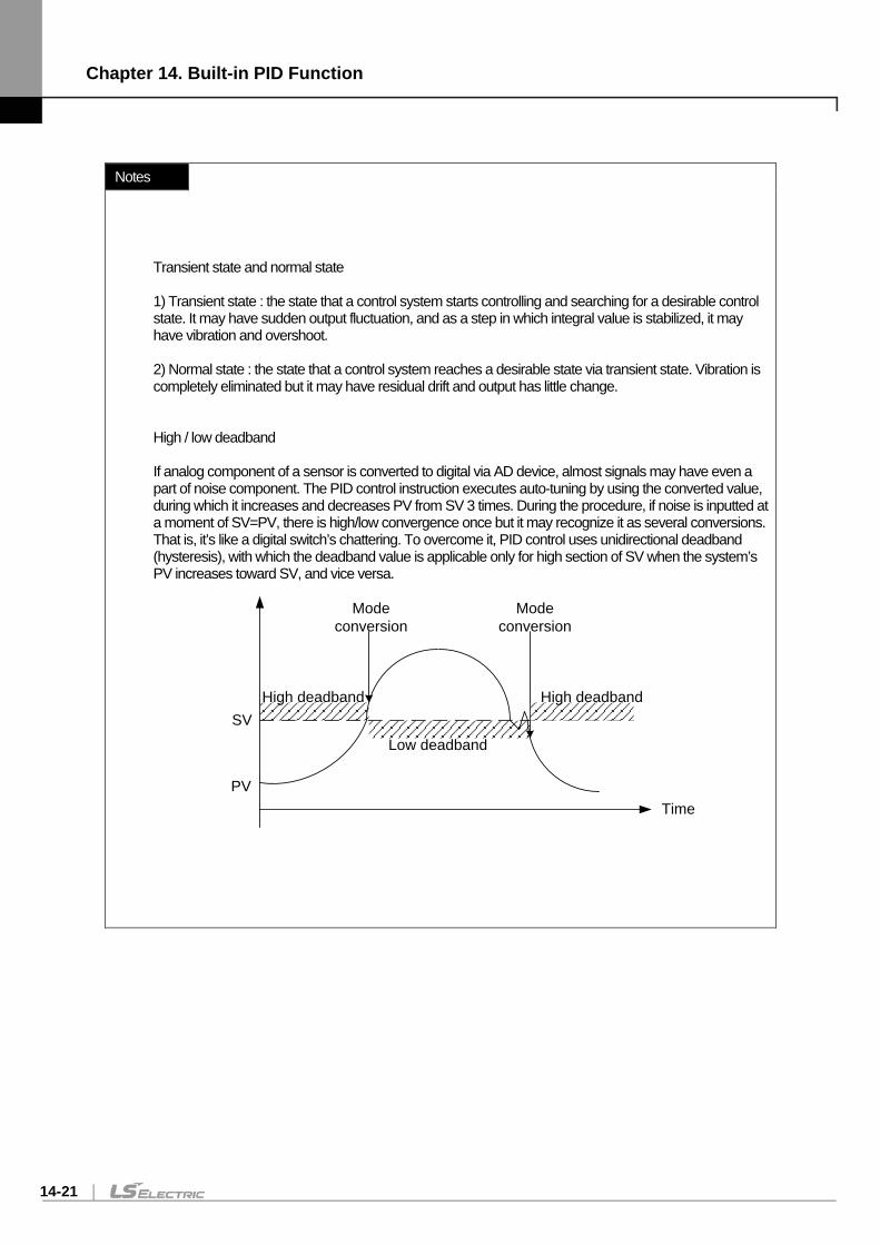
Chapter 14. Built-in PID Function
14-21
Notes
Transient state and normal state 1) Transient state : the state that a control system starts controlling and searching for a desirable control state. It may have sudden output fluctuation, and as a step in which integral value is stabilized, it may have vibration and overshoot. 2) Normal state : the state that a control system reaches a desirable state via transient state. Vibration is completely eliminated but it may have residual drift and output has little change. High / low deadband If analog component of a sensor is converted to digital via AD device, almost signals may have even a part of noise component. The PID control instruction executes auto-tuning by using the converted value, during which it increases and decreases PV from SV 3 times. During the procedure, if noise is inputted at a moment of SV=PV, there is high/low convergence once but it may recognize it as several conversions. That is, it’s like a digital switch’s chattering. To overcome it, PID control uses unidirectional deadband (hysteresis), with which the deadband value is applicable only for high section of SV when the system’s PV increases toward SV, and vice versa.
Time
SV
PV
Mode conversion
Mode conversion
High deadband
Low deadband
High deadband
Chapter 14. Built-in PID Function
14-22
14.6 Convenient Functions of PID Instruction The chapter describes additional functions that may be conveniently used with PID instructions.
14.6.1 Various control methods including PID The most commonly used PID controls are P control, PD control and PID control. Meanwhile, if expecting several characteristics(mostly stabilization), ID control, I control and D control, which are slightly complicate than the above-listed controls, are often used. To enable various controls, PIDRUN instructions support the function to allow or prohibit such controls by P, I and D components. For instance, in case of P control, it may be structured by setting _PID[B]_[L]Ti and _PID[B]_[L]Td as 0. If PI control is desired, set _PID[B]_[L]Kp and _PID[B]_[L]Ti only and input 0 to _PID[B]_[L]Td. Then, if you wish to use ID control, set _PID[B]_[L]Kp as 0 and set the remaining _PID[B]_[L]Ti and _PID[B]_[L]Td. Likewise, ID control sets 0 to _PID[B]_[L]Kp and substitutes each ID control coefficient to _PID[B]_[L]Ti and _PID[B]_[L]Td. However, interestingly, ID control has 0 output theoretically once setting 0 to _PID[B]_[L]Kp(refer to equation 14.3.2 through 14.3.5). In addition, actual PIDRUN instruction calculates MVp = 0 and K_p = 1 internally if inputting 0 to _PID[B]_[L]Kp, enabling ID control, I control and D control.
14.6.2 Operation and function of Anti Wind – up PIDRUN instruction supports two wind-up prevention functions; Anti Wind-up 1 and Anti Wind-up 2. The former one that is basically supported may work for controls including I control, PI control, ID control and PID control and may not be cancelled. The operation principle is to limit MVi(integral result) to _PID[B]_[L]MV_max and _PID[B]_[L]MV_min. On the other hand, Anti Wind-up 2 is organically connected MVp(proportional term result). If only with MVp, MV may reach 土(_PID[B]_[L]MV_max) because of a large system error, MVi maintains the previous value without any calculation. Therefore, if an error is large, it induces PV to move to SV only with MVp, not integral nor differential, resumes I control and prevents MVi from being excessively accumulated. On the other hand, a user may cancel an operation if Anti Wind-up 2 makes _PID[B]_[L]AW2D bit on the common bit area ON. And, like PI control and PID control, it works for a control accompanying with P control and I control.
14.6.3 Operation and function of Auto-tuning PIDRUN instruction has the AT function that tests a system through several basic settings and calculates _PID[B]_[L]T_s, _PID[B]_[L]K_p, _PID[B]_[L]T_i and _PID[B]_[L]T_d, suitable for the system. The values such as _PID[B]_[L]MV_min, _PID[B]_[L]MV_max, _PID[B]_[L]AT_HYS_val and _PID[B]_[L]AT_SV should be set before AT while the AT function sets MV three times in good order of _PID[B]_[L]MV_max and _PID[B]_[L]MV_min, operates it, checks the system’s state(PV) response, measures the time and vibration degree to reach to the AT target value(AT_ST) and finally, calculates _PID[B]_[L]T_s, _PID[B]_[L]K_p, _PID[B]_[L]T_i and _PID[B]_[L]T_d suitable for the measurements. To calculate the accurate tuning value, refer to the AT setting described in 14.7.4 and induce the AT operation accordingly.
Notes
Auto-tuning
At the moment when a series of works end, AT may automatically substitutes _PID[B]_[L]T_s, _PID[B]_[L]K_p, _PID[B]_[L]T_i and _PID[B]_[L]T_d, which are calculated, to the corresponding positions, so a user must note that _PID[B]_[L]T_s, _PID[B]_[L]K_p, _PID[B]_[L]T_i and _PID[B]_[L]T_d that are used before are to be eliminated.
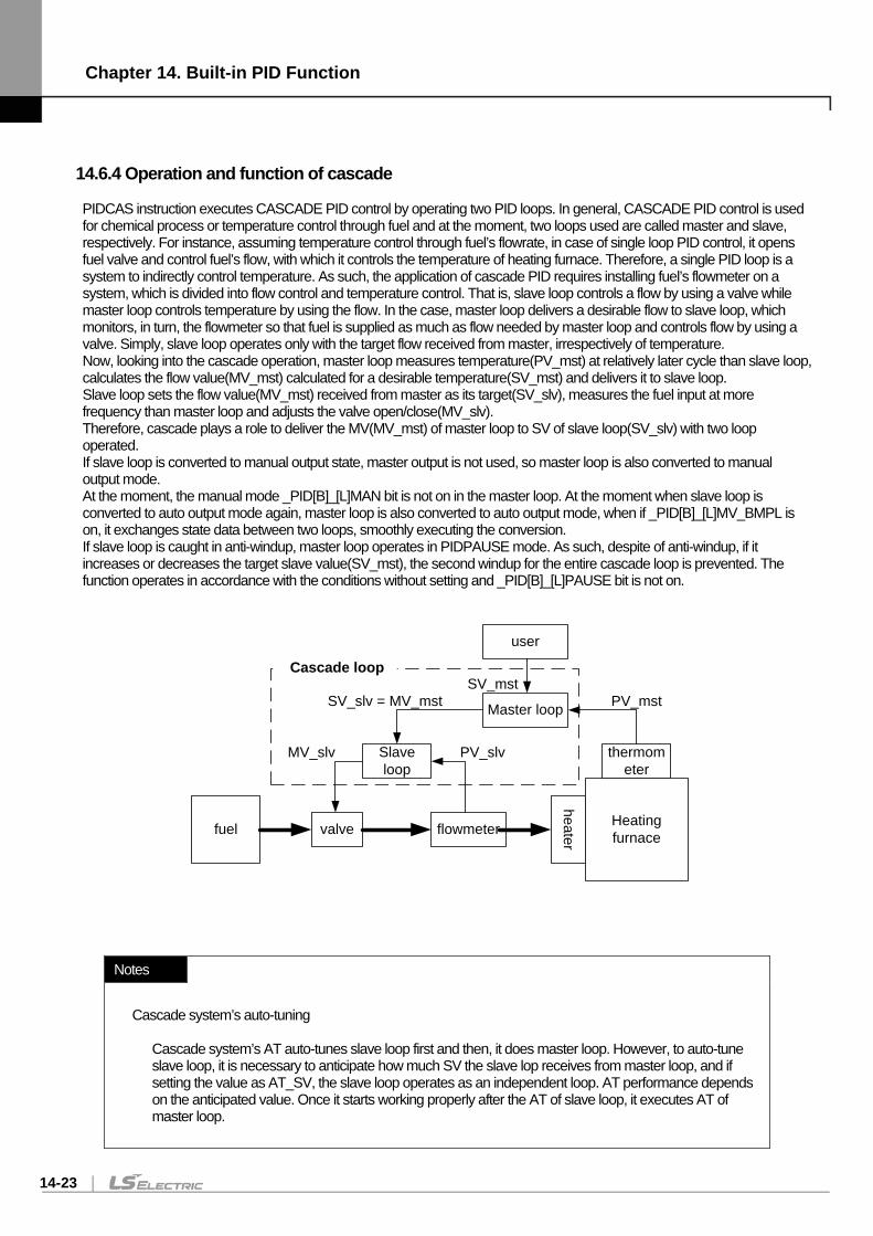
Chapter 14. Built-in PID Function
14-23
14.6.4 Operation and function of cascade PIDCAS instruction executes CASCADE PID control by operating two PID loops. In general, CASCADE PID control is used for chemical process or temperature control through fuel and at the moment, two loops used are called master and slave, respectively. For instance, assuming temperature control through fuel’s flowrate, in case of single loop PID control, it opens fuel valve and control fuel’s flow, with which it controls the temperature of heating furnace. Therefore, a single PID loop is a system to indirectly control temperature. As such, the application of cascade PID requires installing fuel’s flowmeter on a system, which is divided into flow control and temperature control. That is, slave loop controls a flow by using a valve while master loop controls temperature by using the flow. In the case, master loop delivers a desirable flow to slave loop, which monitors, in turn, the flowmeter so that fuel is supplied as much as flow needed by master loop and controls flow by using a valve. Simply, slave loop operates only with the target flow received from master, irrespectively of temperature. Now, looking into the cascade operation, master loop measures temperature(PV_mst) at relatively later cycle than slave loop, calculates the flow value(MV_mst) calculated for a desirable temperature(SV_mst) and delivers it to slave loop. Slave loop sets the flow value(MV_mst) received from master as its target(SV_slv), measures the fuel input at more frequency than master loop and adjusts the valve open/close(MV_slv). Therefore, cascade plays a role to deliver the MV(MV_mst) of master loop to SV of slave loop(SV_slv) with two loop operated. If slave loop is converted to manual output state, master output is not used, so master loop is also converted to manual output mode. At the moment, the manual mode _PID[B]_[L]MAN bit is not on in the master loop. At the moment when slave loop is converted to auto output mode again, master loop is also converted to auto output mode, when if _PID[B]_[L]MV_BMPL is on, it exchanges state data between two loops, smoothly executing the conversion. If slave loop is caught in anti-windup, master loop operates in PIDPAUSE mode. As such, despite of anti-windup, if it increases or decreases the target slave value(SV_mst), the second windup for the entire cascade loop is prevented. The function operates in accordance with the conditions without setting and _PID[B]_[L]PAUSE bit is not on.
Master loop
Slave loop
valve flowmeter
heater
Heating furnace
thermometer
fuel
PV_mst
user
SV_mstSV_slv = MV_mst
MV_slv PV_slv
Cascade loop
Notes
Cascade system’s auto-tuning Cascade system’s AT auto-tunes slave loop first and then, it does master loop. However, to auto-tune slave loop, it is necessary to anticipate how much SV the slave lop receives from master loop, and if setting the value as AT_SV, the slave loop operates as an independent loop. AT performance depends on the anticipated value. Once it starts working properly after the AT of slave loop, it executes AT of master loop.
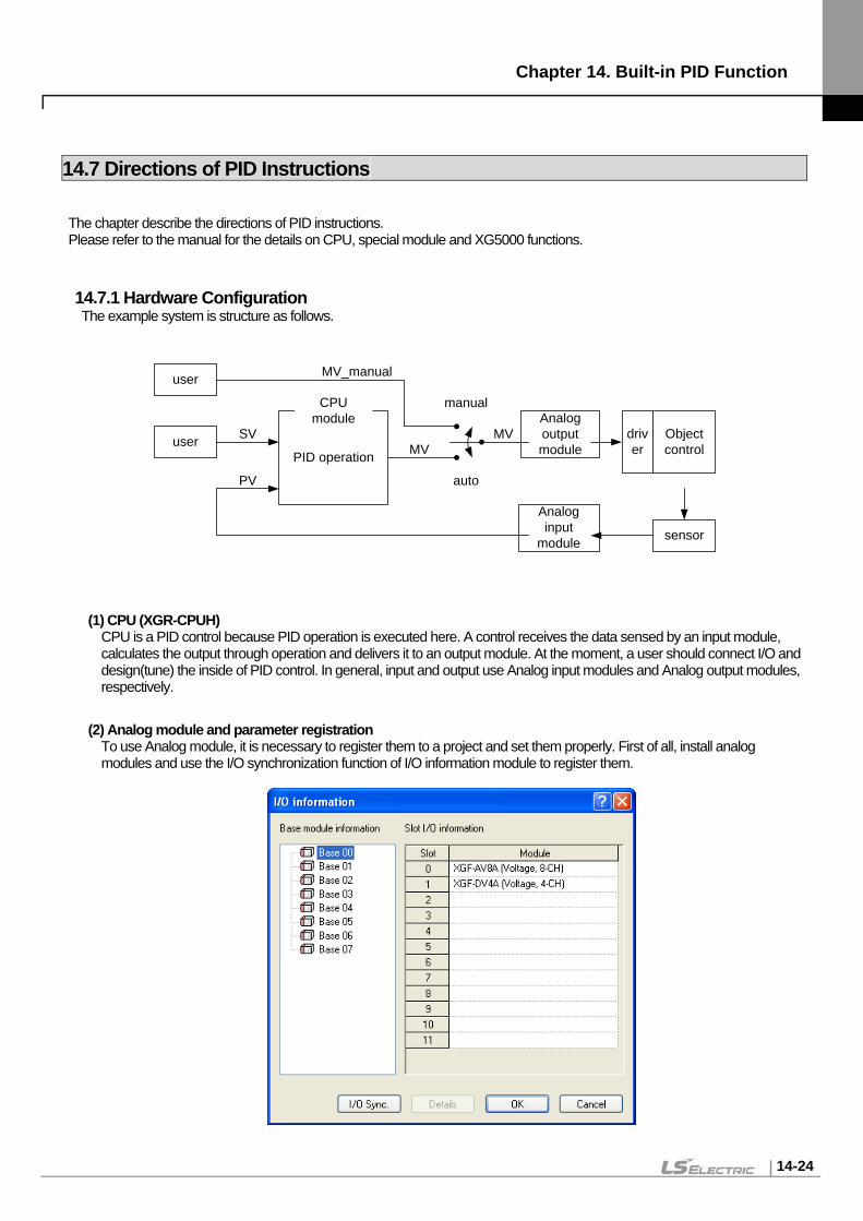
Chapter 14. Built-in PID Function
14-24
14.7 Directions of PID Instructions The chapter describe the directions of PID instructions. Please refer to the manual for the details on CPU, special module and XG5000 functions.
14.7.1 Hardware Configuration The example system is structure as follows.
user SV
PID operation
CPU module
sensor
Analog input
module
Analog output module
Object control
PV
user
auto
manual
MV_manual
MVMV driv
er
(1) CPU (XGR-CPUH) CPU is a PID control because PID operation is executed here. A control receives the data sensed by an input module, calculates the output through operation and delivers it to an output module. At the moment, a user should connect I/O and design(tune) the inside of PID control. In general, input and output use Analog input modules and Analog output modules, respectively.
(2) Analog module and parameter registration To use Analog module, it is necessary to register them to a project and set them properly. First of all, install analog modules and use the I/O synchronization function of I/O information module to register them.
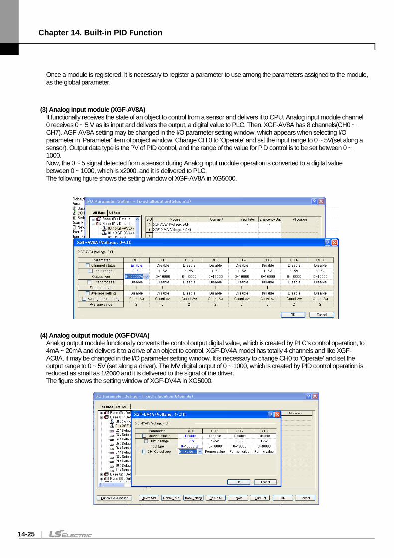
Chapter 14. Built-in PID Function
14-25
Once a module is registered, it is necessary to register a parameter to use among the parameters assigned to the module, as the global parameter.
(3) Analog input module (XGF-AV8A) It functionally receives the state of an object to control from a sensor and delivers it to CPU. Analog input module channel 0 receives 0 ~ 5 V as its input and delivers the output, a digital value to PLC. Then, XGF-AV8A has 8 channels(CH0 ~ CH7). AGF-AV8A setting may be changed in the I/O parameter setting window, which appears when selecting I/O parameter in ‘Parameter’ item of project window. Change CH 0 to ‘Operate’ and set the input range to 0 ~ 5V(set along a sensor). Output data type is the PV of PID control, and the range of the value for PID control is to be set between 0 ~ 1000. Now, the 0 ~ 5 signal detected from a sensor during Analog input module operation is converted to a digital value between 0 ~ 1000, which is x2000, and it is delivered to PLC. The following figure shows the setting window of XGF-AV8A in XG5000.
(4) Analog output module (XGF-DV4A) Analog output module functionally converts the control output digital value, which is created by PLC’s control operation, to 4mA ~ 20mA and delivers it to a drive of an object to control. XGF-DV4A model has totally 4 channels and like XGF-AC8A, it may be changed in the I/O parameter setting window. It is necessary to change CH0 to ‘Operate’ and set the output range to 0 ~ 5V (set along a driver). The MV digital output of 0 ~ 1000, which is created by PID control operation is reduced as small as 1/2000 and it is delivered to the signal of the driver. The figure shows the setting window of XGF-DV4A in XG5000.
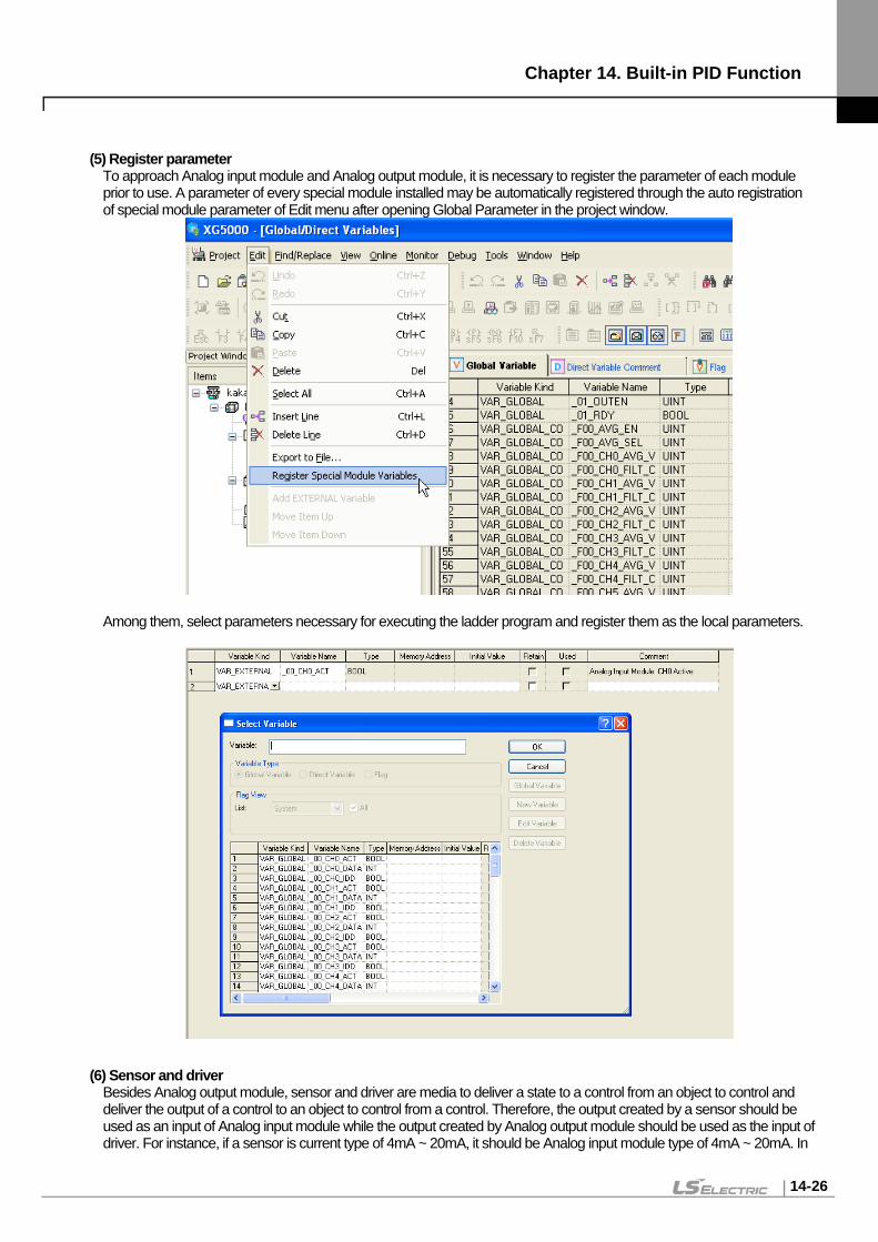
Chapter 14. Built-in PID Function
14-26
(5) Register parameter To approach Analog input module and Analog output module, it is necessary to register the parameter of each module prior to use. A parameter of every special module installed may be automatically registered through the auto registration of special module parameter of Edit menu after opening Global Parameter in the project window.
Among them, select parameters necessary for executing the ladder program and register them as the local parameters.
(6) Sensor and driver Besides Analog output module, sensor and driver are media to deliver a state to a control from an object to control and deliver the output of a control to an object to control from a control. Therefore, the output created by a sensor should be used as an input of Analog input module while the output created by Analog output module should be used as the input of driver. For instance, if a sensor is current type of 4mA ~ 20mA, it should be Analog input module type of 4mA ~ 20mA. In
Chapter 14. Built-in PID Function
14-27
addition, if a driver is voltage type of 0V ~ 5V, Analog output module should be also voltage type of 0V ~ 5V. The output of Analog output module is used as a drive signal of a driver. If it is used directly as the motive power of driver, PLC may be subject to malfunction.
(7) Object to control The system uses water level control system as its object to control. The water level system is designed to supply water to a water tank of which bottom is slightly open and maintain a desirable water level. The water in a tank uniformly flows out and the increase/decrease of water depends on the water inflow by means of a pump. The structure of the water control system is as follows.
pumpinflow
outflow
Water level
Water level
sensordriver
Water tank
14.7.2 Program example 1
The figure shows a program example to execute PID control by using Analog input module and Analog output module. (but, PID constant and SV value are set in the parameter monitor window in the program)
L1 : delivers Analog input data to PV of PIDRUN instruction by using constant On contact. L5 : If %MX0 bit is on, it executes the control operation of PIDRUN block 0 and loop 0 and if it is complete, it activates D/A output. If D/A output is deactivated, the module outputs the value set when it is registered. L10 : Delivers MV output of PIDRUN instruction to Analog output data by using constant ON contact.
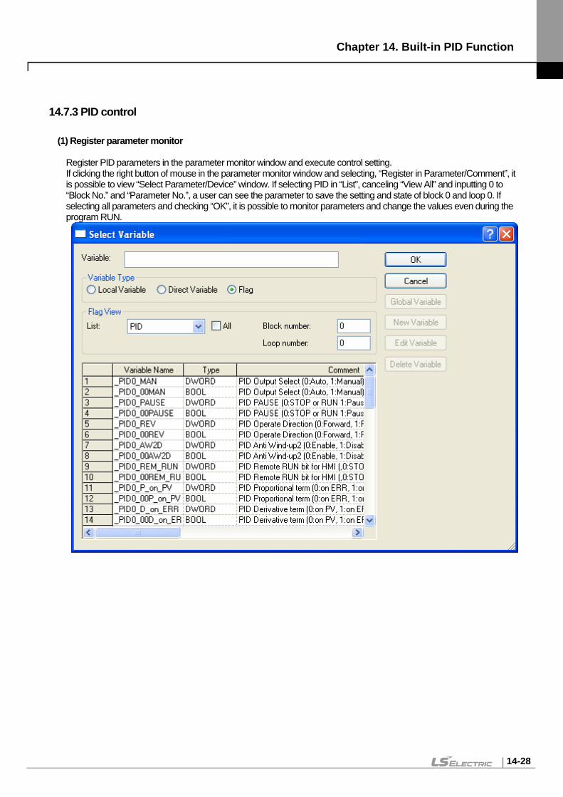
Chapter 14. Built-in PID Function
14-28
14.7.3 PID control
(1) Register parameter monitor Register PID parameters in the parameter monitor window and execute control setting. If clicking the right button of mouse in the parameter monitor window and selecting, “Register in Parameter/Comment”, it is possible to view “Select Parameter/Device” window. If selecting PID in “List”, canceling “View All” and inputting 0 to “Block No.” and “Parameter No.”, a user can see the parameter to save the setting and state of block 0 and loop 0. If selecting all parameters and checking “OK”, it is possible to monitor parameters and change the values even during the program RUN.
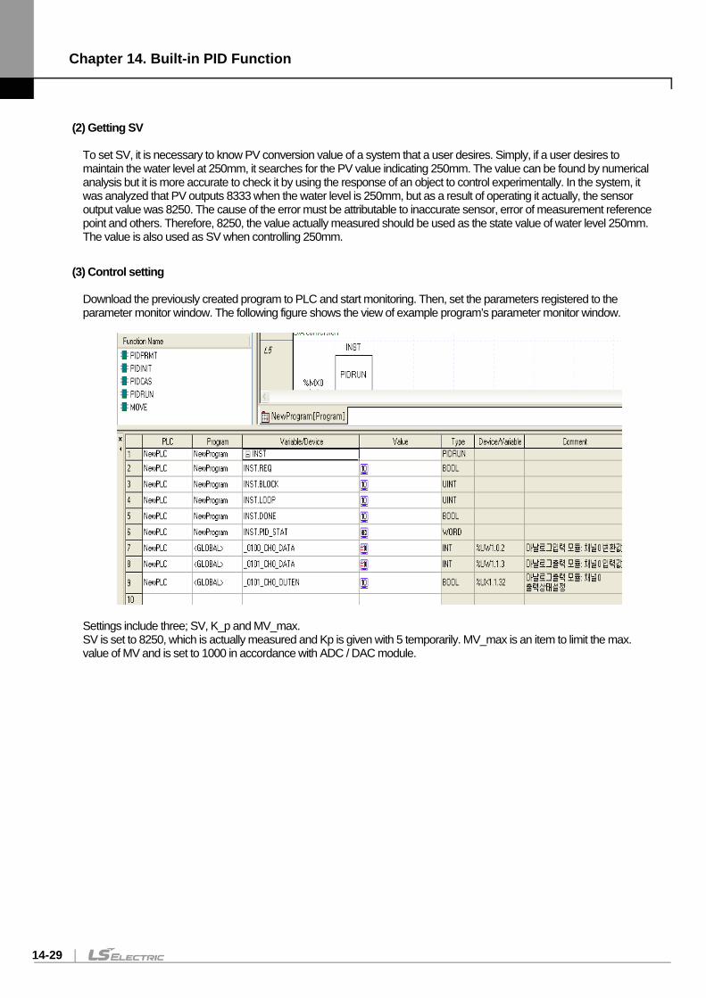
Chapter 14. Built-in PID Function
14-29
(2) Getting SV To set SV, it is necessary to know PV conversion value of a system that a user desires. Simply, if a user desires to maintain the water level at 250mm, it searches for the PV value indicating 250mm. The value can be found by numerical analysis but it is more accurate to check it by using the response of an object to control experimentally. In the system, it was analyzed that PV outputs 8333 when the water level is 250mm, but as a result of operating it actually, the sensor output value was 8250. The cause of the error must be attributable to inaccurate sensor, error of measurement reference point and others. Therefore, 8250, the value actually measured should be used as the state value of water level 250mm. The value is also used as SV when controlling 250mm.
(3) Control setting Download the previously created program to PLC and start monitoring. Then, set the parameters registered to the parameter monitor window. The following figure shows the view of example program’s parameter monitor window.
Settings include three; SV, K_p and MV_max. SV is set to 8250, which is actually measured and Kp is given with 5 temporarily. MV_max is an item to limit the max. value of MV and is set to 1000 in accordance with ADC / DAC module.
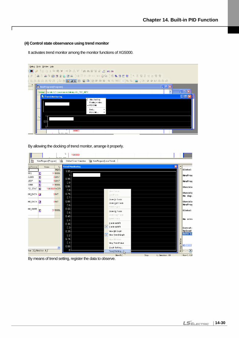
Chapter 14. Built-in PID Function
14-30
(4) Control state observance using trend monitor It activates trend monitor among the monitor functions of XG5000.
By allowing the docking of trend monitor, arrange it properly.
By means of trend setting, register the data to observe.
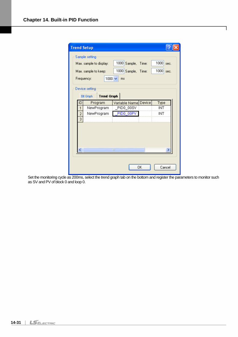
Chapter 14. Built-in PID Function
14-31
Set the monitoring cycle as 200ms, select the trend graph tab on the bottom and register the parameters to monitor such as SV and PV of block 0 and loop 0.
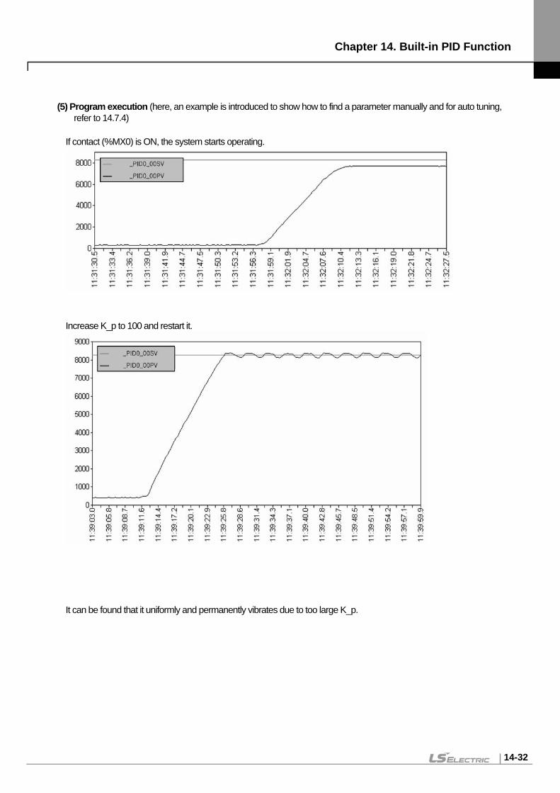
Chapter 14. Built-in PID Function
14-32
(5) Program execution (here, an example is introduced to show how to find a parameter manually and for auto tuning, refer to 14.7.4)
If contact (%MX0) is ON, the system starts operating.
Increase K_p to 100 and restart it.
It can be found that it uniformly and permanently vibrates due to too large K_p.
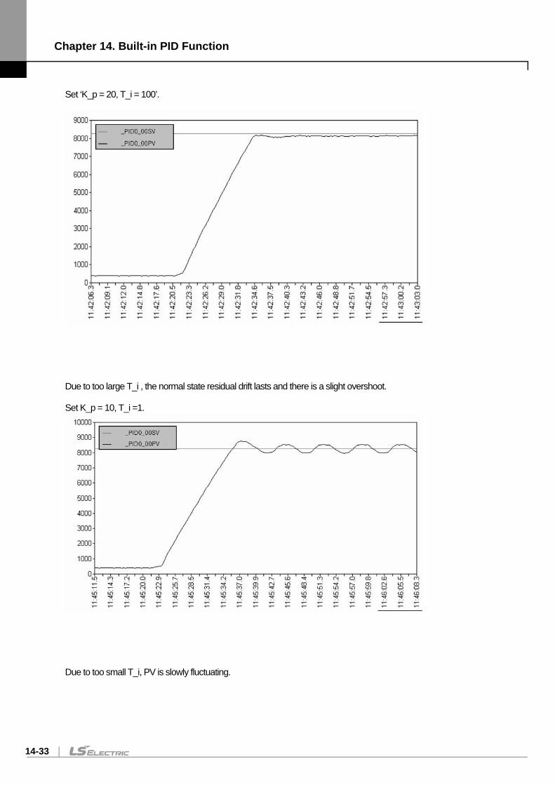
Chapter 14. Built-in PID Function
14-33
Set ‘K_p = 20, T_i = 100’.
Due to too large T_i , the normal state residual drift lasts and there is a slight overshoot. Set K_p = 10, T_i =1.
Due to too small T_i, PV is slowly fluctuating.
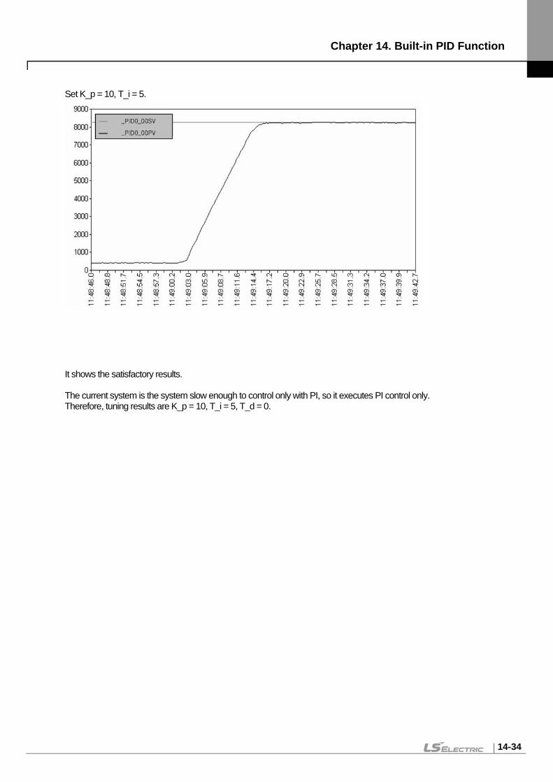
Chapter 14. Built-in PID Function
14-34
Set K_p = 10, T_i = 5.
It shows the satisfactory results. The current system is the system slow enough to control only with PI, so it executes PI control only. Therefore, tuning results are K_p = 10, T_i = 5, T_d = 0.
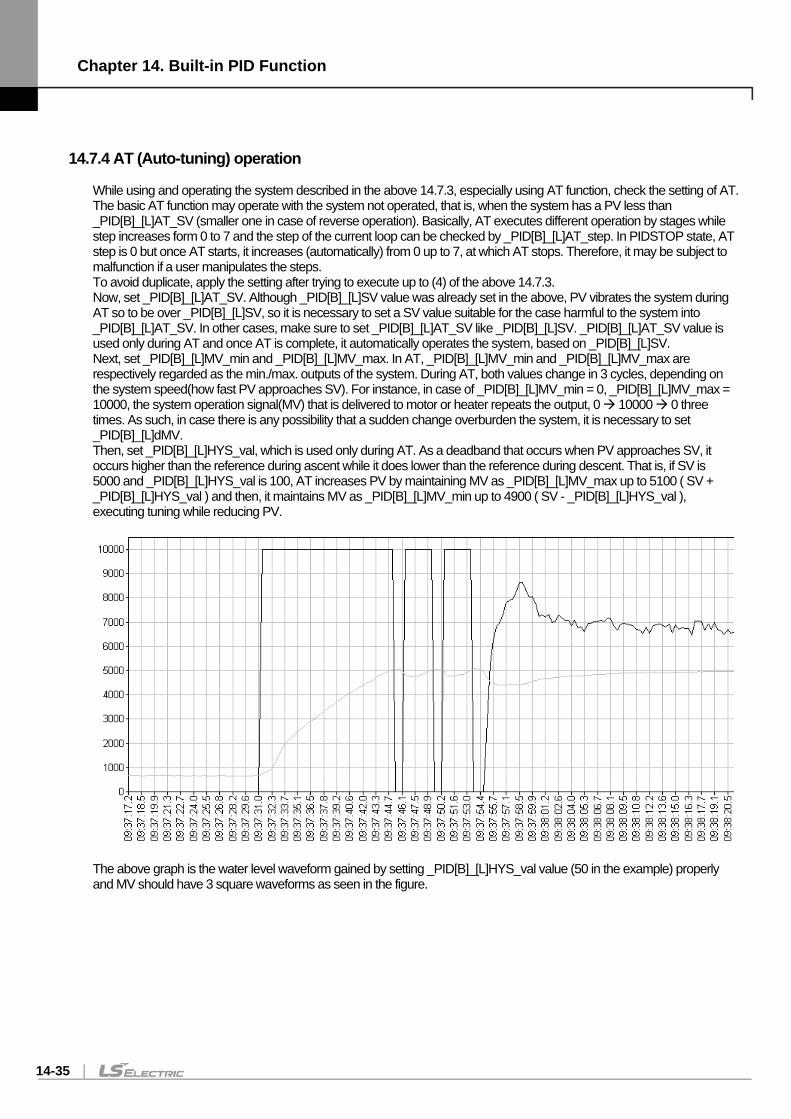
Chapter 14. Built-in PID Function
14-35
14.7.4 AT (Auto-tuning) operation
While using and operating the system described in the above 14.7.3, especially using AT function, check the setting of AT. The basic AT function may operate with the system not operated, that is, when the system has a PV less than _PID[B]_[L]AT_SV (smaller one in case of reverse operation). Basically, AT executes different operation by stages while step increases form 0 to 7 and the step of the current loop can be checked by _PID[B]_[L]AT_step. In PIDSTOP state, AT step is 0 but once AT starts, it increases (automatically) from 0 up to 7, at which AT stops. Therefore, it may be subject to malfunction if a user manipulates the steps. To avoid duplicate, apply the setting after trying to execute up to (4) of the above 14.7.3. Now, set _PID[B]_[L]AT_SV. Although _PID[B]_[L]SV value was already set in the above, PV vibrates the system during AT so to be over _PID[B]_[L]SV, so it is necessary to set a SV value suitable for the case harmful to the system into _PID[B]_[L]AT_SV. In other cases, make sure to set _PID[B]_[L]AT_SV like _PID[B]_[L]SV. _PID[B]_[L]AT_SV value is used only during AT and once AT is complete, it automatically operates the system, based on _PID[B]_[L]SV. Next, set _PID[B]_[L]MV_min and _PID[B]_[L]MV_max. In AT, _PID[B]_[L]MV_min and _PID[B]_[L]MV_max are respectively regarded as the min./max. outputs of the system. During AT, both values change in 3 cycles, depending on the system speed(how fast PV approaches SV). For instance, in case of _PID[B]_[L]MV_min = 0, _PID[B]_[L]MV_max = 10000, the system operation signal(MV) that is delivered to motor or heater repeats the output, 0 10000 0 three times. As such, in case there is any possibility that a sudden change overburden the system, it is necessary to set _PID[B]_[L]dMV. Then, set _PID[B]_[L]HYS_val, which is used only during AT. As a deadband that occurs when PV approaches SV, it occurs higher than the reference during ascent while it does lower than the reference during descent. That is, if SV is 5000 and _PID[B]_[L]HYS_val is 100, AT increases PV by maintaining MV as _PID[B]_[L]MV_max up to 5100 ( SV + _PID[B]_[L]HYS_val ) and then, it maintains MV as _PID[B]_[L]MV_min up to 4900 ( SV - _PID[B]_[L]HYS_val ), executing tuning while reducing PV.
The above graph is the water level waveform gained by setting _PID[B]_[L]HYS_val value (50 in the example) properly and MV should have 3 square waveforms as seen in the figure.
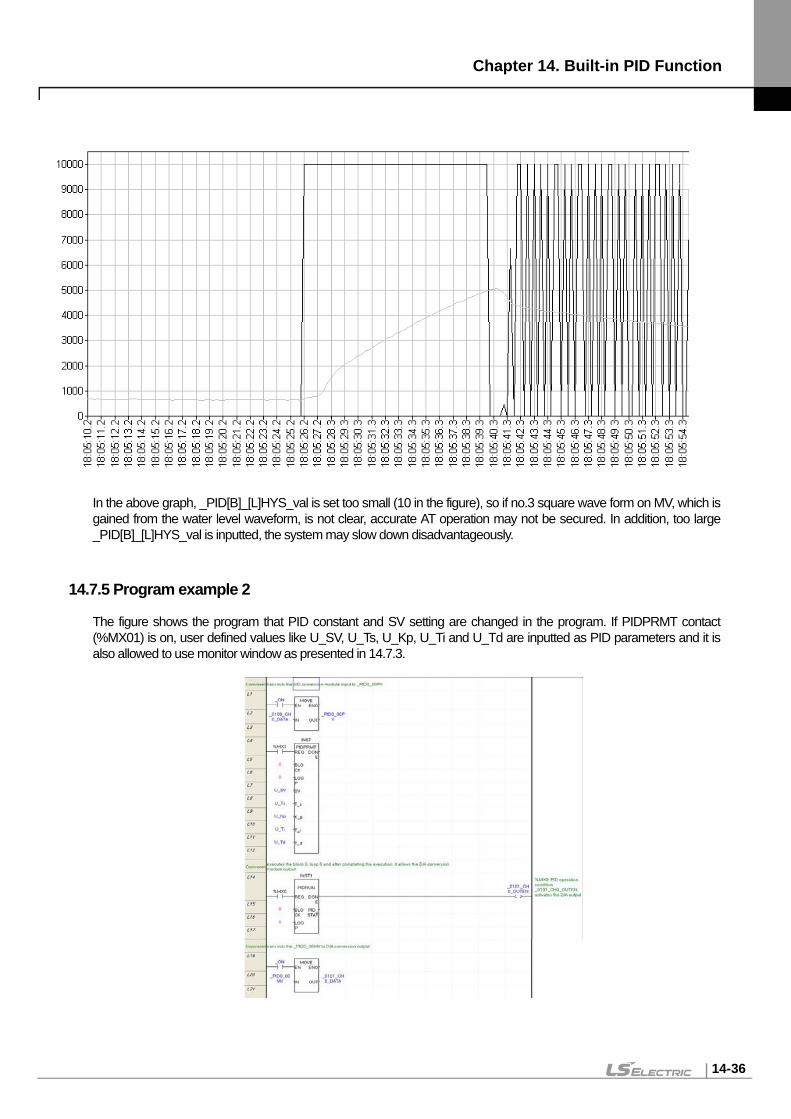
Chapter 14. Built-in PID Function
14-36
In the above graph, _PID[B]_[L]HYS_val is set too small (10 in the figure), so if no.3 square wave form on MV, which is gained from the water level waveform, is not clear, accurate AT operation may not be secured. In addition, too large _PID[B]_[L]HYS_val is inputted, the system may slow down disadvantageously.
14.7.5 Program example 2 The figure shows the program that PID constant and SV setting are changed in the program. If PIDPRMT contact (%MX01) is on, user defined values like U_SV, U_Ts, U_Kp, U_Ti and U_Td are inputted as PID parameters and it is also allowed to use monitor window as presented in 14.7.3.
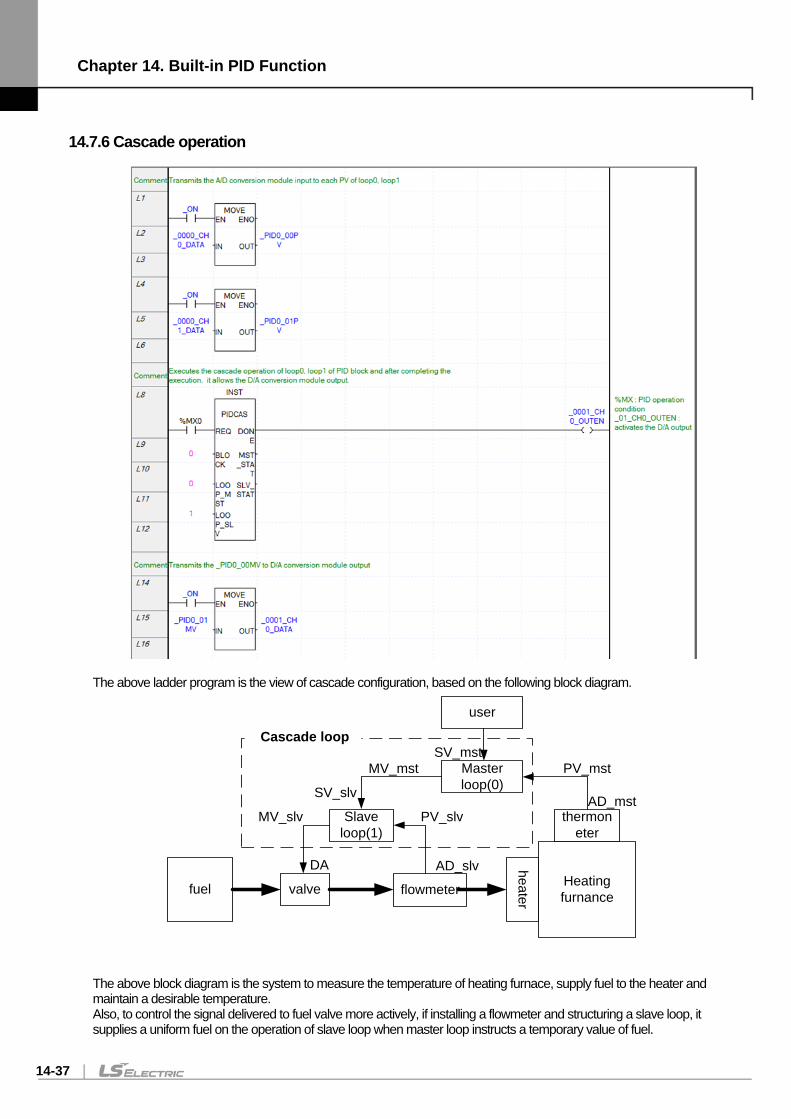
Chapter 14. Built-in PID Function
14-37
14.7.6 Cascade operation
The above ladder program is the view of cascade configuration, based on the following block diagram.
Master loop(0)
Slave loop(1)
valve flowmeter
heater
Heating furnance
thermoneter
fuel
PV_mst
user
SV_mst
MV_slv PV_slv
Cascade loop
DA AD_slv
AD_mst
MV_mst
SV_slv
The above block diagram is the system to measure the temperature of heating furnace, supply fuel to the heater and maintain a desirable temperature. Also, to control the signal delivered to fuel valve more actively, if installing a flowmeter and structuring a slave loop, it supplies a uniform fuel on the operation of slave loop when master loop instructs a temporary value of fuel.

Chapter 14. Built-in PID Function
14-38
Chapter 15. Troubleshooting
15-1
Chapter 15 Troubleshooting The chapter describes types of potential errors that occur while operating the system, causes of errors, how to detect them and corrective measures.
15.1 Basic Troubleshooting Procedure To improve the reliability of a system, it is important to take a corrective measure promptly if a trouble occurs as well as to use highly reliable devices. To operate a system immediately, it is the most important to quickly detect potential causes of a trouble and take corrective measures. To troubleshoot the system correctly, make sure to take the following cautions and procedures. (1) Check by visual inspection Please check the followings visually. • Operation status(Stop, Run) • Power On/Off status • I/O device status • Wiring status(I/O wiring, expansion and communication cable) • Check the status of each display(POWER LED, RUN/STOP LED, I/O LED and etc), connect to peripherals and check the
operation condition and program (2) Check any abnormality Please observe how a fault changes by executing the followings. • Move the key switch to STOP and turn it On/Off (3) Restricting Range Estimate by which factor a fault occurs by the following methods. • Is it from the PLC or external factor? • I/O module or others? • PLC program?
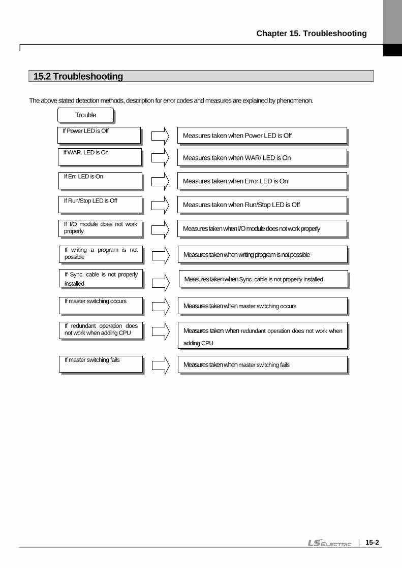
Chapter 15. Troubleshooting
15-2
15.2 Troubleshooting The above stated detection methods, description for error codes and measures are explained by phenomenon.
Trouble
If Power LED is Off
If WAR. LED is On
If Err. LED is On
If Run/Stop LED is Off
Measures taken when Power LED is Off
Measures taken when WAR/ LED is On
Measures taken when Error LED is On
Measures taken when Run/Stop LED is Off
If I/O module does not work properly Measures taken when I/O module does not work properly
If writing a program is not possible Measures taken when writing program is not possible
If redundant operation does not work when adding CPU Measures taken when redundant operation does not work when
adding CPU
If master switching occurs Measures taken when master switching occurs
If Sync. cable is not properly installed
Measures taken when Sync. cable is not properly installed
If master switching fails Measures taken when master switching fails
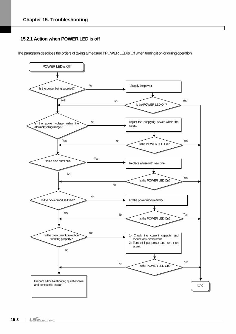
Chapter 15. Troubleshooting
15-3
15.2.1 Action when POWER LED is off The paragraph describes the orders of taking a measure if POWER LED is Off when turning it on or during operation.
POWER LED is Off
Is the power being supplied?
Is the power voltage within the allowable voltage range?
Has a fuse burnt out?
Is the power module fixed?
Is the overcurrent protection working properly?
Prepare a troubleshooting questionnaire and contact the dealer.
Supply the power
Is the POWER LED On?
Adjust the supplying power within the range.
Replace a fuse with new one.
Fix the power module firmly.
Is the POWER LED On?
Is the POWER LED On?
Is the POWER LED On?
1) Check the current capacity and reduce any overcurrent.
2) Turn off input power and turn it on again.
Is the POWER LED On?
No
No
No
Yes No
No
No
No
No
No
Yes Yes
Yes
Yes
Yes
Yes
Yes
Yes
End
Yes
No
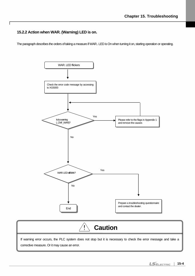
Chapter 15. Troubleshooting
15-4
15.2.2 Action when WAR. (Warning) LED is on. The paragraph describes the orders of taking a measure if WAR.. LED is On when turning it on, starting operation or operating.
WAR. LED flickers
Yes
No
Is it a warning (_CNF_WAR)?
No
Check the error code message by accessing to XG5000
WAR. LED still blink?
Prepare a troubleshooting questionnaire and contact the dealer.
Please refer to the flags in Appendix 1 and remove the causes
End
Yes
If warning error occurs, the PLC system does not stop but it is necessary to check the error message and take a
corrective measure. Or it may cause an error.
Caution
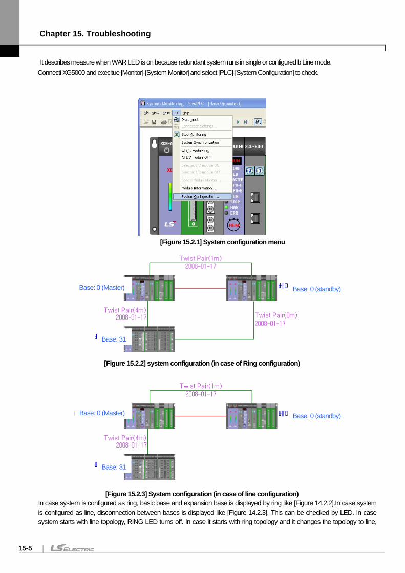
Chapter 15. Troubleshooting
15-5
It describes measure when WAR LED is on because redundant system runs in single or configured b Line mode. Connecti XG5000 and execitue [Monitor]-[System Monitor] and select [PLC]-[System Configuration] to check.
[Figure 15.2.1] System configuration menu
[Figure 15.2.2] system configuration (in case of Ring configuration)
[Figure 15.2.3] System configuration (in case of line configuration) In case system is configured as ring, basic base and expansion base is displayed by ring like [Figure 14.2.2].In case system is configured as line, disconnection between bases is displayed like [Figure 14.2.3]. This can be checked by LED. In case system starts with line topology, RING LED turns off. In case it starts with ring topology and it changes the topology to line,
Base: 0 (standby)
Base: 0 (standby)
Base: 0 (Master)
Base: 0 (Master)
Base: 31
Base: 31

Chapter 15. Troubleshooting
15-6
RING LED flickers
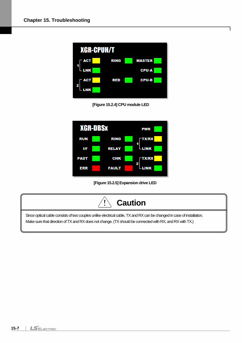
Chapter 15. Troubleshooting
15-7
[Figure 15.2.4] CPU module LED
[Figure 15.2.5] Expansion drive LED
Since optical cable consists of two couples unlike electrical cable, TX and RX can be changed in case of installation. Make sure that direction of TX and RX does not change. (TX should be connected with RX, and RX with TX.)
Caution
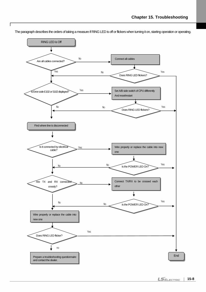
Chapter 15. Troubleshooting
15-8
The paragraph describes the orders of taking a measure if RING LED is off or flickers when turning it on, starting operation or operating.
RING LED is Off
Are all cables connected?
Is Error code E102 or S102 displayed?
Is it connected by electrical cable?
Are TX and RX connected
crossly?
Wire properly or replace the cable into
new one
Connect all cables
Does RING LED flickers?
Set A/B side switch of CPU differently
And reset/restart
Wire properly or replace the cable into new
one
Does RING LED flickers?
Is the POWER LED On?
Connect TX/RX to be crossed each
other
Is the POWER LED On?
No
Yes
No
No No
Yes
No
No No
Yes Yes
Yes
Yes
Yes
No
No
End
Find where line is disconnected
Does RING LED flicker?
Prepare a troubleshooting questionnaire and contact the dealer.
Yes
no
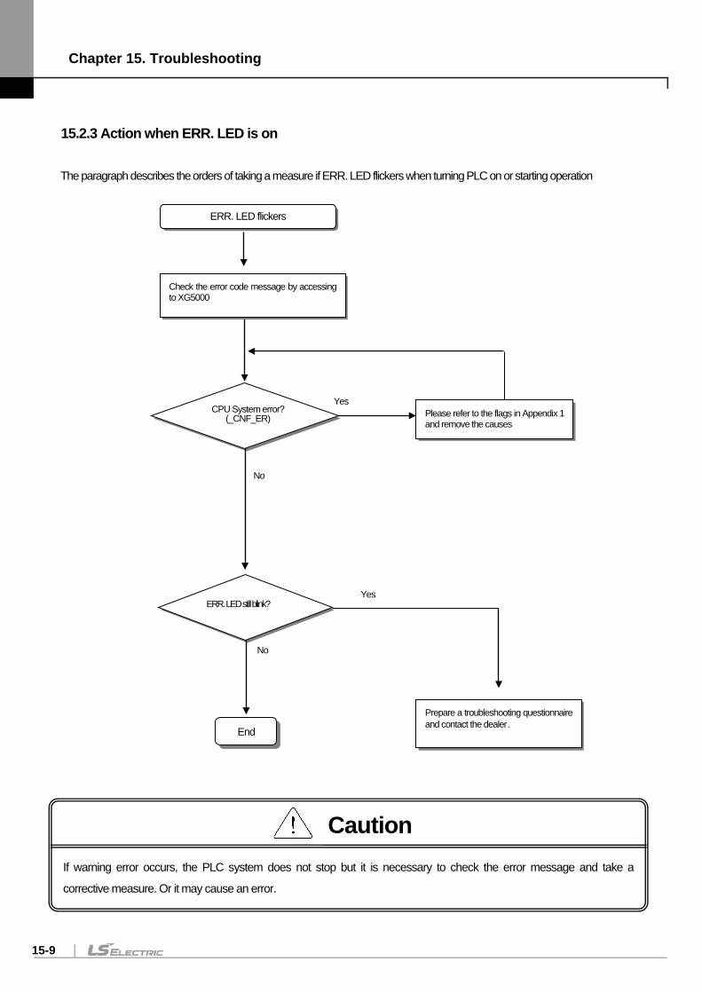
Chapter 15. Troubleshooting
15-9
15.2.3 Action when ERR. LED is on The paragraph describes the orders of taking a measure if ERR. LED flickers when turning PLC on or starting operation
ERR. LED flickers
Yes
No
No
Check the error code message by accessing to XG5000
ERR. LED still blink?
Prepare a troubleshooting questionnaire and contact the dealer.
Please refer to the flags in Appendix 1 and remove the causes
End
Yes
If warning error occurs, the PLC system does not stop but it is necessary to check the error message and take a
corrective measure. Or it may cause an error.
Caution
CPU System error? (_CNF_ER)
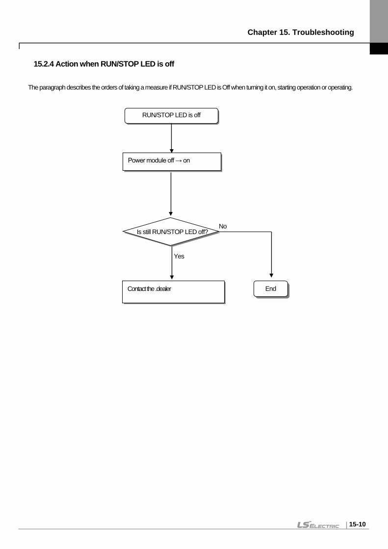
Chapter 15. Troubleshooting
15-10
15.2.4 Action when RUN/STOP LED is off The paragraph describes the orders of taking a measure if RUN/STOP LED is Off when turning it on, starting operation or operating.
RUN/STOP LED is off
No
Yes
Contact the .dealer End
Power module off → on
Is still RUN/STOP LED off?
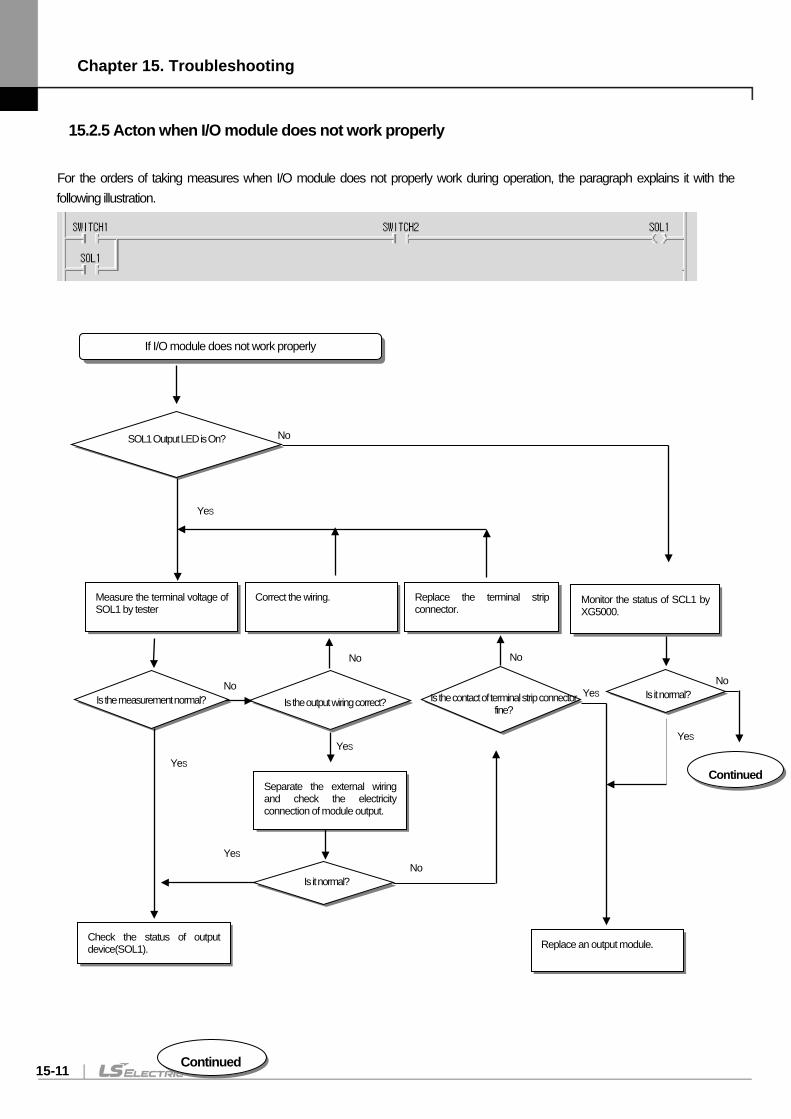
Chapter 15. Troubleshooting
15-11
15.2.5 Acton when I/O module does not work properly For the orders of taking measures when I/O module does not properly work during operation, the paragraph explains it with the following illustration.
If I/O module does not work properly
Monitor the status of SCL1 by XG5000.
SOL1 Output LED is On? No
Replace the terminal strip connector.
Measure the terminal voltage of SOL1 by tester
Correct the wiring.
Yes
Is the measurement normal? Is the output wiring correct? Is the contact of terminal strip connector fine?
Is it normal?
Separate the external wiring and check the electricity connection of module output.
Is it normal?
Check the status of output device(SOL1). Replace an output module.
Continued Yes
No
Yes
No
Yes No
Yes
Yes
No
No
Continued
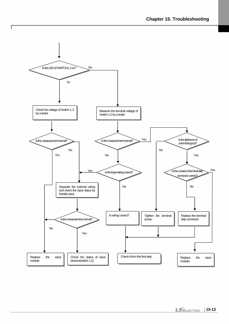
Chapter 15. Troubleshooting
15-12
Is the LED of SWITCH1, 2 on? No
Check the voltage of Switch 1, 2 by a tester
Yes
Is the measurement normal?
Separate the external wiring and check the input status by forcible input.
Is the measurement normal?
Check the status of input devices(switch 1,2).
Replace the input module.
Measure the terminal voltage of Switch 1,2 by a tester
Is the measurement normal? Is the tightness of a terminal good?
Is the input wiring correct?
Is wiring correct? Tighten the terminal screw.
Replace the terminal strip connector.
Replace the input module.
Check it from the first step
Is the contact of terminal strip
connector correct?
Ye
No No
Yes
No Yes
Yes
No
Yes No
No
Yes
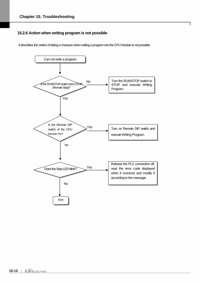
Chapter 15. Troubleshooting
15-13
15.2.6 Action when writing program is not possible It describes the orders of taking a measure when writing a program into the CPU Module is not possible.
Can not write a program
Yes
Turn the RUN/STOP switch to STOP and execute Writing Program.
Is the RUN/STOP switch set to STOP (Remote Stop)?
No
Does the Stop LED blink? Release the PLC connection off, read the error code displayed when it connects and modify it according to the message.
Yes
End
No
Is the Remote DIP switch of the CPU Module On?
Turn on Remote DIP switch and
execute Writing Program.
Yes
No
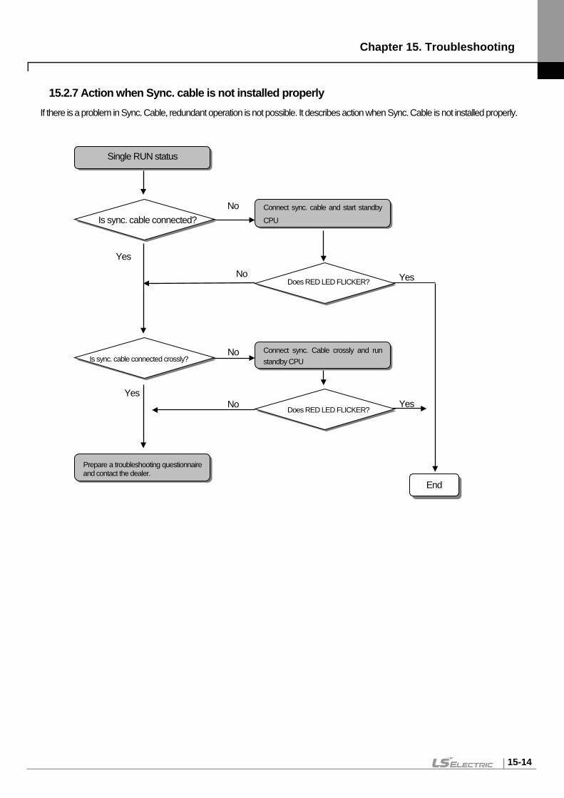
Chapter 15. Troubleshooting
15-14
15.2.7 Action when Sync. cable is not installed properly If there is a problem in Sync. Cable, redundant operation is not possible. It describes action when Sync. Cable is not installed properly.
Single RUN status
No Yes
End
Is sync. cable connected? Connect sync. cable and start standby
CPU
Connect sync. Cable crossly and run standby CPU
Prepare a troubleshooting questionnaire and contact the dealer.
Yes
No
No
Yes
Yes
Is sync. cable connected crossly?
Does RED LED FLICKER?
Does RED LED FLICKER?
No
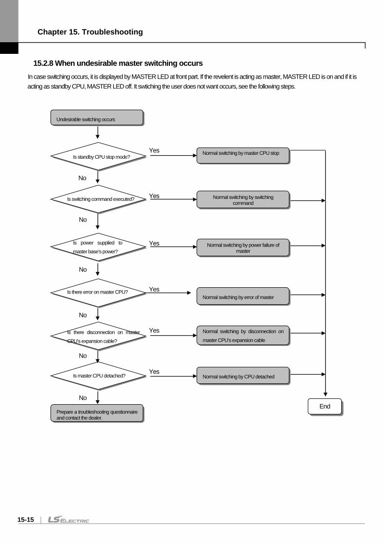
Chapter 15. Troubleshooting
15-15
15.2.8 When undesirable master switching occurs In case switching occurs, it is displayed by MASTER LED at front part. If the revelent is acting as master, MASTER LED is on and if it is acting as standby CPU, MASTER LED off. It swtiching the user does not want occurs, see the following steps.
Undesirable switching occurs
Yes
End
Is standby CPU stop mode? Normal switching by master CPU stop
Normal switching by switching command
Normal switching by disconnection on
master CPU’s expansion cable
Yes
No
Is switching command executed?
Is power supplied to
master base’s power?
Is there error on master CPU?
Normal switching by error of master
Normal switching by CPU detached
Normal switching by power failure of master
No
No
No
No
Yes
Yes
Yes
Yes
Yes
Is there disconnection on master
CPU’s expansion cable?
Is master CPU detached?
Prepare a troubleshooting questionnaire and contact the dealer.
No
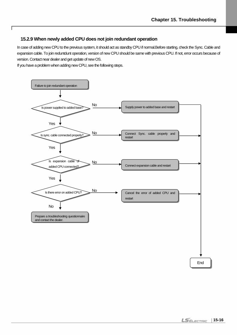
Chapter 15. Troubleshooting
15-16
15.2.9 When newly added CPU does not join redundant operation In case of adding new CPU to the previous system, it should act as standby CPU if normal.Before starting, check the Sync. Cable and expansion cable. To join reduntdunt operation, version of new CPU should be same with previous CPU. If not, error occurs because of version. Contact near dealer and get update of new OS. If you have a problem when adding new CPU, see the following steps.
Failure to join redundant operation
Yes
End
Is power supplied to added base? Supply power to added base and restart
Connect Sync. cable properly and restart
No
Yes
Is sync. cable connected properly?
Is expansion cable of
added CPU connected?
Is there error on added CPU? Cancel the error of added CPU and
restart
Connect expansion cable and restart
Yes
Yes
No
No
No
No
Prepare a troubleshooting questionnaire and contact the dealer.
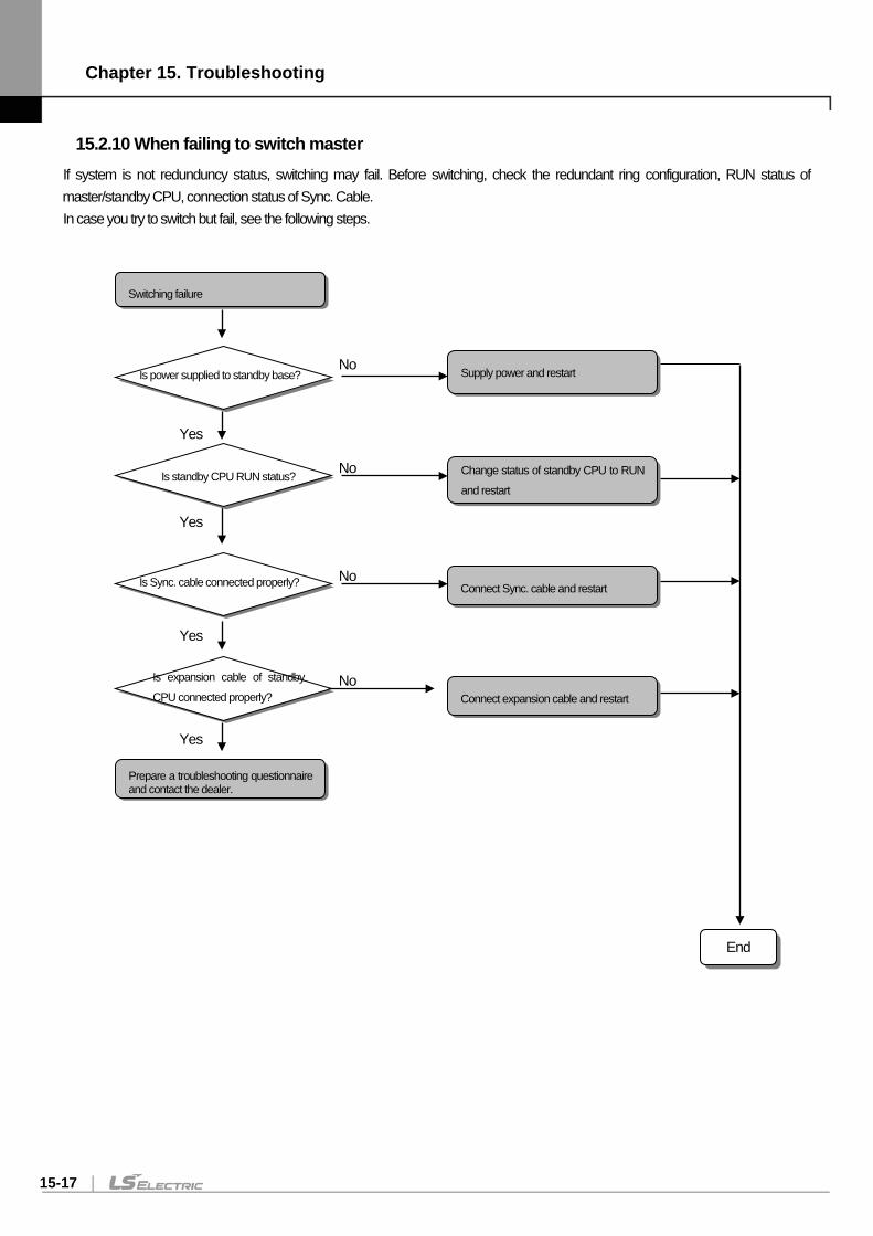
Chapter 15. Troubleshooting
15-17
15.2.10 When failing to switch master If system is not redunduncy status, switching may fail. Before switching, check the redundant ring configuration, RUN status of master/standby CPU, connection status of Sync. Cable. In case you try to switch but fail, see the following steps.
Switching failure
Yes
End
Is power supplied to standby base? Supply power and restart
Change status of standby CPU to RUN
and restart
No
Yes
Is standby CPU RUN status?
Is Sync. cable connected properly?
Is expansion cable of standby
CPU connected properly?
Connect expansion cable and restart
Connect Sync. cable and restart
Yes
Yes
Yes
No
No
No
Prepare a troubleshooting questionnaire and contact the dealer.
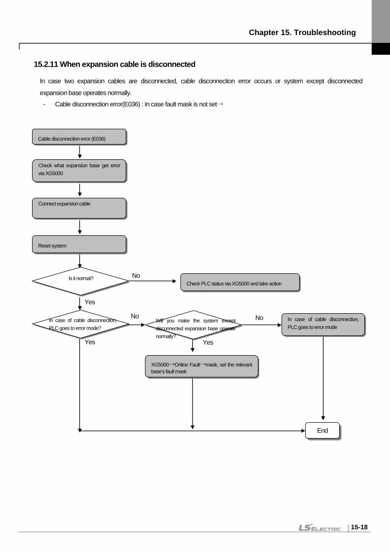
Chapter 15. Troubleshooting
15-18
15.2.11 When expansion cable is disconnected
In case two expansion cables are disconnected, cable disconnection error occurs or system except disconnected
expansion base operates normally.
- Cable disconnection error(E036) : In case fault mask is not set→
Cable disconnection error (E036)
Yes
End
Will you make the system except disconnected expansion base operate normally?
Check what expansion base get error via XG5000
Connect expansion cable
Is it normal?
In case of cable disconnection, PLC goes to error mode?
Check PLC status via XG5000 and take action
Reset system
Yes Yes
No
No
XG5000→Online Fault→mask, set the relevant base’s fault mask
In case of cable disconnection, PLC goes to error mode
No
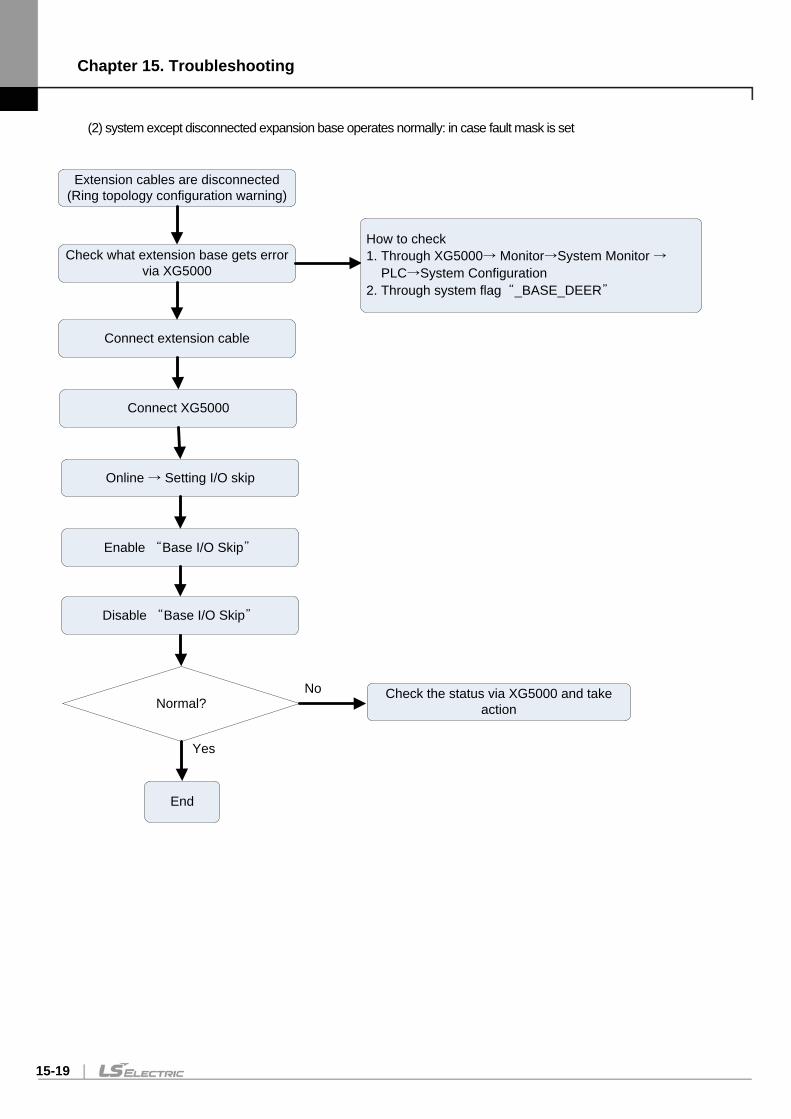
Chapter 15. Troubleshooting
15-19
(2) system except disconnected expansion base operates normally: in case fault mask is set
Extension cables are disconnected(Ring topology configuration warning)
Normal?
Check what extension base gets error via XG5000
Connect extension cable
Yes
No Check the status via XG5000 and take action
How to check1. Through XG5000→ Monitor→System Monitor → PLC→System Configuration2. Through system flag“_BASE_DEER”
Connect XG5000
Online → Setting I/O skip
Enable “Base I/O Skip”
Disable “Base I/O Skip”
End
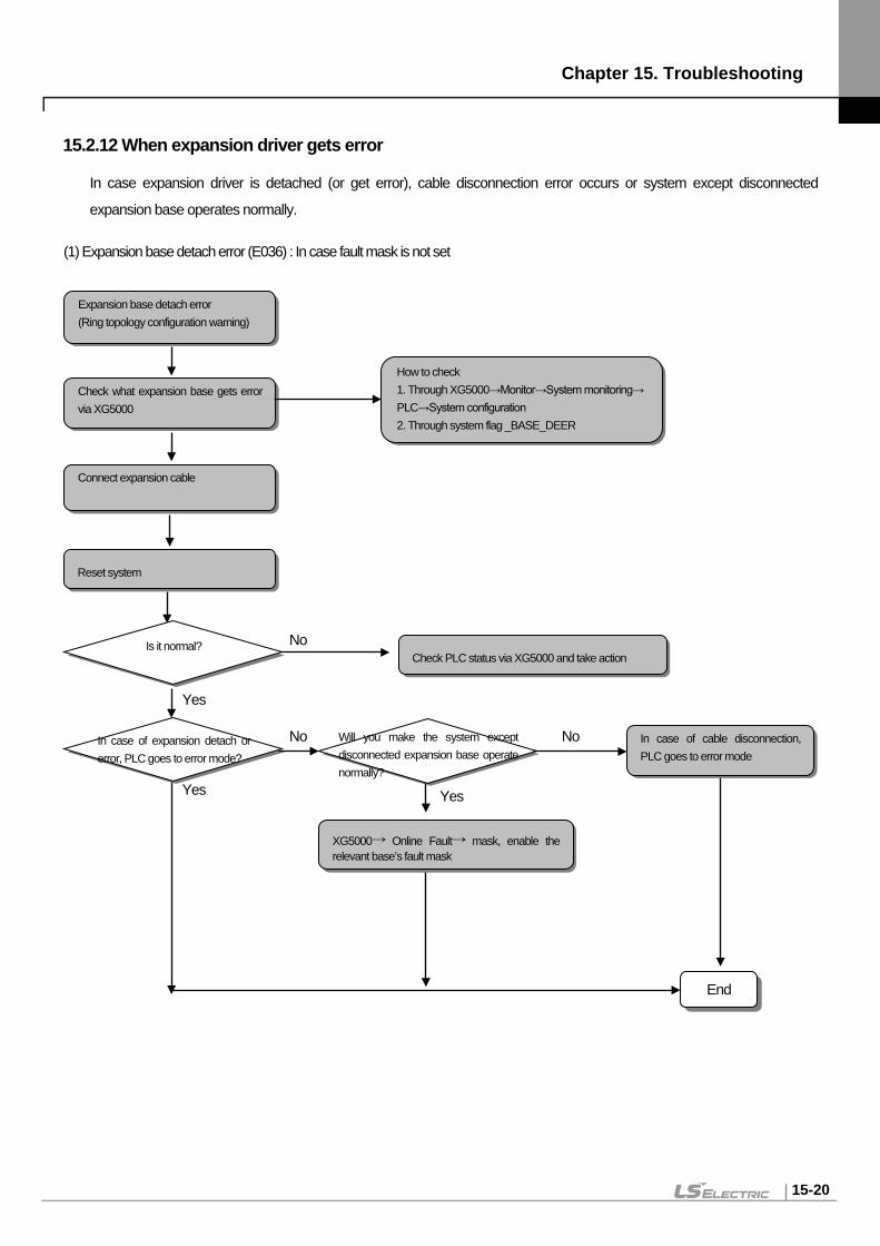
Chapter 15. Troubleshooting
15-20
15.2.12 When expansion driver gets error
In case expansion driver is detached (or get error), cable disconnection error occurs or system except disconnected
expansion base operates normally. (1) Expansion base detach error (E036) : In case fault mask is not set
Expansion base detach error (Ring topology configuration warning)
Yes
End
Will you make the system except disconnected expansion base operate normally?
Check what expansion base gets error via XG5000
Connect expansion cable
Is it normal?
In case of expansion detach or error, PLC goes to error mode?
Check PLC status via XG5000 and take action
Reset system
Yes Yes
No
No
XG5000→ Online Fault→ mask, enable the relevant base’s fault mask
In case of cable disconnection, PLC goes to error mode
How to check 1. Through XG5000→Monitor→System monitoring→ PLC→System configuration 2. Through system flag _BASE_DEER
No
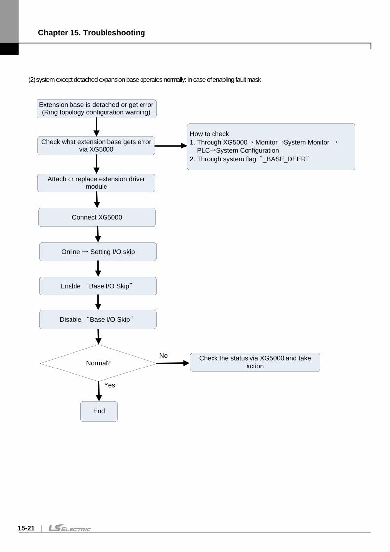
Chapter 15. Troubleshooting
15-21
(2) system except detached expansion base operates normally: in case of enabling fault mask
Extension base is detached or get error(Ring topology configuration warning)
Normal?
Check what extension base gets error via XG5000
Attach or replace extension driver module
Yes
No Check the status via XG5000 and take action
How to check1. Through XG5000→ Monitor→System Monitor → PLC→System Configuration2. Through system flag“_BASE_DEER”
Connect XG5000
Online → Setting I/O skip
Enable “Base I/O Skip”
Disable “Base I/O Skip”
End
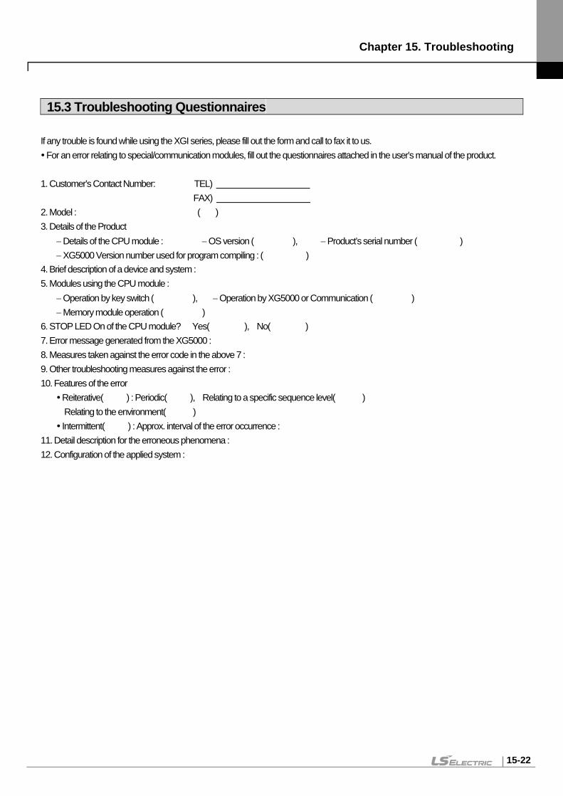
Chapter 15. Troubleshooting
15-22
15.3 Troubleshooting Questionnaires If any trouble is found while using the XGI series, please fill out the form and call to fax it to us. For an error relating to special/communication modules, fill out the questionnaires attached in the user’s manual of the product. 1. Customer’s Contact Number: TEL) FAX) 2. Model : ( ) 3. Details of the Product − Details of the CPU module : − OS version ( ), − Product’s serial number ( ) − XG5000 Version number used for program compiling : ( ) 4. Brief description of a device and system : 5. Modules using the CPU module : − Operation by key switch ( ), − Operation by XG5000 or Communication ( ) − Memory module operation ( ) 6. STOP LED On of the CPU module? Yes( ), No( ) 7. Error message generated from the XG5000 : 8. Measures taken against the error code in the above 7 : 9. Other troubleshooting measures against the error : 10. Features of the error Reiterative( ) : Periodic( ), Relating to a specific sequence level( ) Relating to the environment( ) Intermittent( ) : Approx. interval of the error occurrence : 11. Detail description for the erroneous phenomena : 12. Configuration of the applied system :
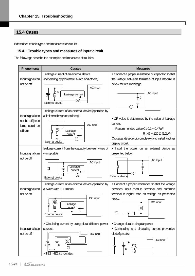
Chapter 15. Troubleshooting
15-23
15.4 Cases It describes trouble types and measures for circuits.
15.4.1 Trouble types and measures of input circuit The followings describe the examples and measures of troubles.
Phenomena Causes Measures Input signal can not be off
Leakage current of an external device (if operating by proximate switch and others)
Connect a proper resistance or capacitor so that the voltage between terminals of input module is below the return voltage. CR value is determined by the value of leakage current. − Recommended value C : 0.1 ~ 0.47uF R : 47 ~ 120 Ω (1/2W) Or, separate a circuit completely and install another display circuit.
Input signal can not be off(neon lamp could be still on)
Leakage current of an external device(operation by a limit switch with neon lamp)
Input signal can not be off
leakage current from the capacity between wires of wiring cable
Install the power on an external device as presented below.
Input signal can not be off
Leakage current of an external device(operation by a switch with LED mark)
Connect a proper resistance so that the voltage between input module terminal and common terminal is higher than off voltage as presented below.
Input signal can not be off
Circulating current by using plural different power sources If E1 > E2, it circulates.
Change plural to singular power Connecting to a circulating current preventive diode(figure below)
External device
DC input
R Leakage current
C
~
External device
AC input
R Leakage current
C
~
External device
AC input
R Leakage current
C
~
AC input
R
~
External device
AC input Leakage current
AC Input
~
External device
DC Input
R
E1
DC Input
L E
DC Input
L
E
E
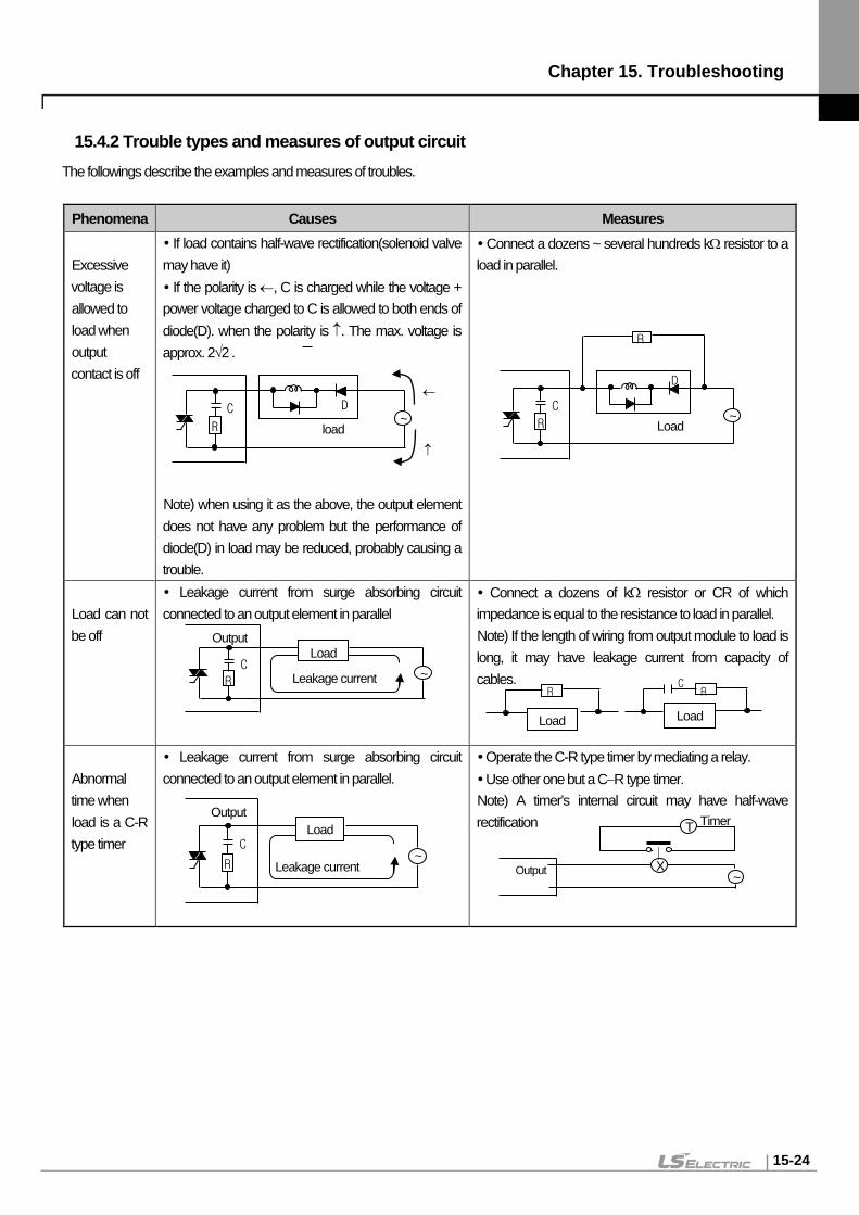
Chapter 15. Troubleshooting
15-24
15.4.2 Trouble types and measures of output circuit The followings describe the examples and measures of troubles.
Phenomena Causes Measures Excessive voltage is allowed to load when output contact is off
If load contains half-wave rectification(solenoid valve may have it) If the polarity is ←, C is charged while the voltage + power voltage charged to C is allowed to both ends of diode(D). when the polarity is ↑. The max. voltage is approx. 2√2 . Note) when using it as the above, the output element does not have any problem but the performance of diode(D) in load may be reduced, probably causing a trouble.
Connect a dozens ~ several hundreds kΩ resistor to a load in parallel.
Load can not be off
Leakage current from surge absorbing circuit connected to an output element in parallel
Connect a dozens of kΩ resistor or CR of which impedance is equal to the resistance to load in parallel. Note) If the length of wiring from output module to load is long, it may have leakage current from capacity of cables.
Abnormal time when load is a C-R type timer
Leakage current from surge absorbing circuit connected to an output element in parallel.
Operate the C-R type timer by mediating a relay. Use other one but a C−R type timer. Note) A timer’s internal circuit may have half-wave rectification
C R
~
Load
Leakage current
Output
C
R ~
Load
Leakage current
Output
R
Load
R
Load
C
~
X
T Timer
Output
C
R ~
←
↑ load
D C
R ~
Load
R
D
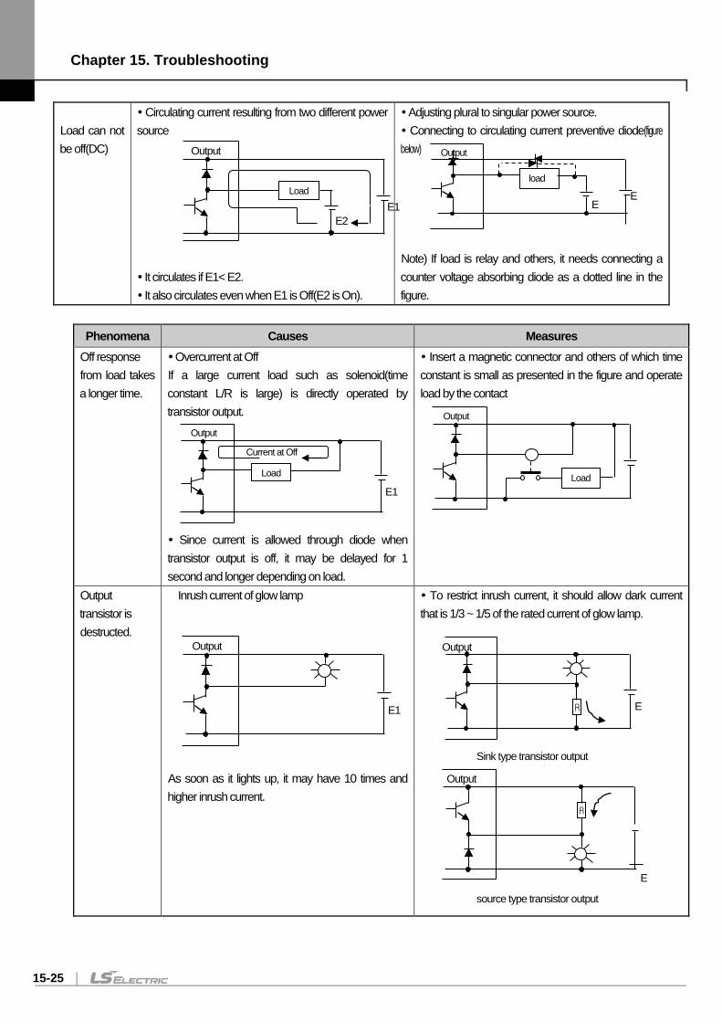
Chapter 15. Troubleshooting
15-25
Load can not be off(DC)
Circulating current resulting from two different power source It circulates if E1< E2. It also circulates even when E1 is Off(E2 is On).
Adjusting plural to singular power source. Connecting to circulating current preventive diode(figure below) Note) If load is relay and others, it needs connecting a counter voltage absorbing diode as a dotted line in the figure.
Phenomena Causes Measures Off response from load takes a longer time.
Overcurrent at Off If a large current load such as solenoid(time constant L/R is large) is directly operated by transistor output. Since current is allowed through diode when transistor output is off, it may be delayed for 1 second and longer depending on load.
Insert a magnetic connector and others of which time constant is small as presented in the figure and operate load by the contact
Output transistor is destructed.
Inrush current of glow lamp As soon as it lights up, it may have 10 times and higher inrush current.
To restrict inrush current, it should allow dark current that is 1/3 ~ 1/5 of the rated current of glow lamp.
Sink type transistor output
source type transistor output
Output
Load
E1
Current at Off
Output
Load
Output
E
R
E
Output
R
Output
E1
Output
load
E E
E1
Load
E2
Output
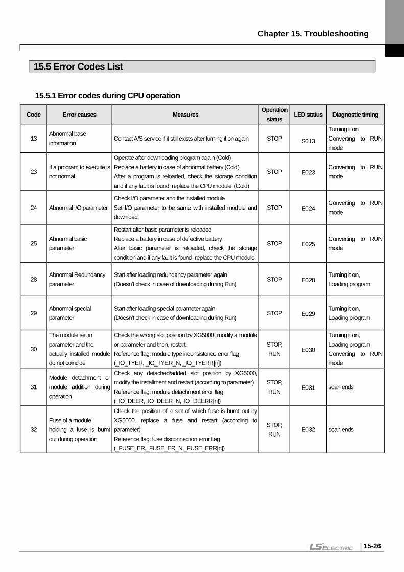
Chapter 15. Troubleshooting
15-26
15.5 Error Codes List
15.5.1 Error codes during CPU operation
Code Error causes Measures Operation
status LED status Diagnostic timing
13 Abnormal base information
Contact A/S service if it still exists after turning it on again STOP S013
Turning it on Converting to RUN mode
23 If a program to execute is not normal
Operate after downloading program again (Cold) Replace a battery in case of abnormal battery (Cold) After a program is reloaded, check the storage condition and if any fault is found, replace the CPU module. (Cold)
STOP E023 Converting to RUN mode
24 Abnormal I/O parameter Check I/O parameter and the installed module Set I/O parameter to be same with installed module and download
STOP E024 Converting to RUN mode
25 Abnormal basic parameter
Restart after basic parameter is reloaded Replace a battery in case of defective battery After basic parameter is reloaded, check the storage condition and if any fault is found, replace the CPU module.
STOP E025 Converting to RUN mode
28 Abnormal Redundancy parameter
Start after loading redundancy parameter again (Doesn’t check in case of downloading during Run)
STOP E028 Turning it on, Loading program
29 Abnormal special parameter
Start after loading special parameter again (Doesn’t check in case of downloading during Run)
STOP E029 Turning it on, Loading program
30
The module set in parameter and the actually installed module do not coincide
Check the wrong slot position by XG5000, modify a module or parameter and then, restart. Reference flag: module type inconsistence error flag (_IO_TYER, _IO_TYER_N, _IO_TYERR[n])
STOP, RUN E030
Turning it on, Loading program Converting to RUN mode
31 Module detachment or module addition during operation
Check any detached/added slot position by XG5000, modify the installment and restart (according to parameter) Reference flag: module detachment error flag (_IO_DEER,_IO_DEER_N,_IO_DEERR[n])
STOP, RUN E031 scan ends
32 Fuse of a module holding a fuse is burnt out during operation
Check the position of a slot of which fuse is burnt out by XG5000, replace a fuse and restart (according to parameter) Reference flag: fuse disconnection error flag (_FUSE_ER,_FUSE_ER_N,_FUSE_ERR[n])
STOP, RUN
E032 scan ends
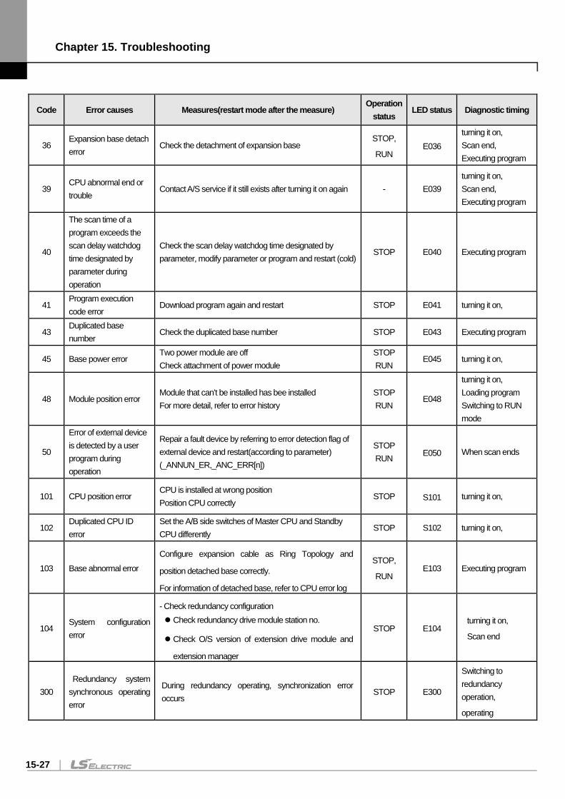
Chapter 15. Troubleshooting
15-27
Code Error causes Measures(restart mode after the measure) Operation
status LED status Diagnostic timing
36 Expansion base detach error
Check the detachment of expansion base STOP,
RUN E036
turning it on, Scan end, Executing program
39 CPU abnormal end or trouble
Contact A/S service if it still exists after turning it on again - E039 turning it on, Scan end, Executing program
40
The scan time of a program exceeds the scan delay watchdog time designated by parameter during operation
Check the scan delay watchdog time designated by parameter, modify parameter or program and restart (cold)
STOP E040 Executing program
41 Program execution code error
Download program again and restart STOP E041 turning it on,
43 Duplicated base number
Check the duplicated base number STOP E043 Executing program
45 Base power error Two power module are off Check attachment of power module
STOP RUN
E045 turning it on,
48 Module position error Module that can’t be installed has bee installed For more detail, refer to error history
STOP RUN
E048
turning it on, Loading program Switching to RUN mode
50
Error of external device is detected by a user program during operation
Repair a fault device by referring to error detection flag of external device and restart(according to parameter) (_ANNUN_ER,_ANC_ERR[n])
STOP RUN E050 When scan ends
101 CPU position error CPU is installed at wrong position Position CPU correctly
STOP S101 turning it on,
102 Duplicated CPU ID error
Set the A/B side switches of Master CPU and Standby CPU differently
STOP S102 turning it on,
103 Base abnormal error Configure expansion cable as Ring Topology and
position detached base correctly.
For information of detached base, refer to CPU error log
STOP,
RUN E103 Executing program
104 System configuration error
- Check redundancy configuration Check redundancy drive module station no.
Check O/S version of extension drive module and
extension manager
STOP E104 turning it on,
Scan end
300 Redundancy system
synchronous operating error
During redundancy operating, synchronization error occurs
STOP E300
Switching to redundancy operation,
operating
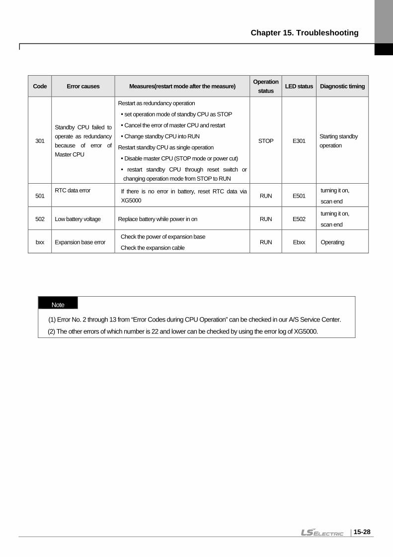
Chapter 15. Troubleshooting
15-28
Code Error causes Measures(restart mode after the measure) Operation
status LED status Diagnostic timing
301
Standby CPU failed to operate as redundancy because of error of Master CPU
Restart as redundancy operation
set operation mode of standby CPU as STOP
Cancel the error of master CPU and restart
Change standby CPU into RUN
Restart standby CPU as single operation
Disable master CPU (STOP mode or power cut)
restart standby CPU through reset switch or changing operation mode from STOP to RUN
STOP E301 Starting standby operation
501 RTC data error
If there is no error in battery, reset RTC data via XG5000
RUN E501 turning it on,
scan end
502 Low battery voltage Replace battery while power in on RUN E502 turning it on,
scan end
bxx Expansion base error Check the power of expansion base
Check the expansion cable RUN Ebxx Operating
Note
(1) Error No. 2 through 13 from “Error Codes during CPU Operation” can be checked in our A/S Service Center.
(2) The other errors of which number is 22 and lower can be checked by using the error log of XG5000.
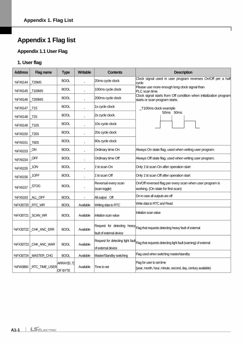
Appendix 1. Flag List
A1-1
Appendix 1 Flag list Appendix 1.1 User Flag
1. User flag
Address Flag name Type Writable Contents Description
%FX6144 _T20MS BOOL - 20ms cycle clock Clock signal used in user program reverses On/Off per a half cycle Please use more enough long clock signal than PLC scan time. Clock signal starts from Off condition when initialization program starts or scan program starts.
_T100ms clock example 50ms 50ms
%FX6145 _T100MS BOOL - 100ms cycle clock
%FX6146 _T200MS BOOL - 200ms cycle clock
%FX6147 _T1S BOOL - 1s cycle clock
%FX6148 _T2S BOOL - 2s cycle clock
%FX6149 _T10S BOOL - 10s cycle clock
%FX6150 _T20S BOOL - 20s cycle clock
%FX6151 _T60S BOOL - 60s cycle clock
%FX6153 _ON BOOL - Ordinary time On Always On state flag, used when writing user program.
%FX6154 _OFF BOOL - Ordinary time Off Always Off state flag, used when writing user program.
%FX6155 _1ON BOOL - 1’st scan On Only 1’st scan On after operation start
%FX6156 _1OFF BOOL - 1’st scan Off Only 1’st scan Off after operation start
%FX6157 _STOG BOOL - Reversal every scan (scan toggle)
On/Off reversed flag per every scan when user program is working. (On state for first scan)
%FX6163 _ALL_OFF BOOL - All output Off On in case all outputs are off
%FX30720 _RTC_WR BOOL Available Writing data to RTC Write data to RTC and Read
%FX30721 _SCAN_WR BOOL Available Initialize scan value Initialize scan value
%FX30722 _CHK_ANC_ERR BOOL Available Request for detecting heavy
fault of external device Flag that requests detecting heavy fault of external
%FX30723 _CHK_ANC_WAR BOOL Available Request for detecting light fault
of external device Flag that requests detecting light fault (warning) of external
%FX30724 _MASTER_CHG BOOL Available Master/Standby switching Flag used when switching master/standby
%FW3860 _RTC_TIME_USER ARRAY[0..7]
OF BYTE Available Time to set
Flag for user to set time (year, month, hour, minute, second, day, century available)
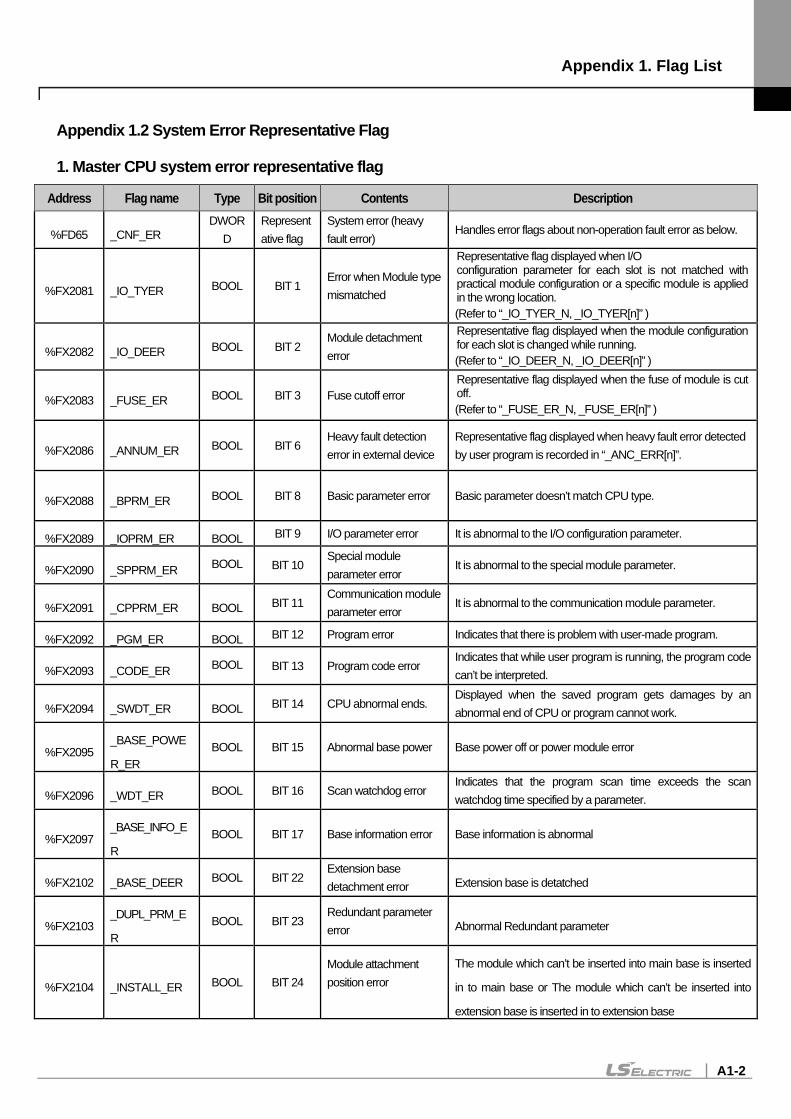
Appendix 1. Flag List
A1-2
Appendix 1.2 System Error Representative Flag
1. Master CPU system error representative flag
Address Flag name Type Bit position Contents Description
%FD65 _CNF_ER DWOR
D Representative flag
System error (heavy fault error)
Handles error flags about non-operation fault error as below.
%FX2081 _IO_TYER BOOL BIT 1 Error when Module type mismatched
Representative flag displayed when I/O configuration parameter for each slot is not matched with practical module configuration or a specific module is applied in the wrong location. (Refer to “_IO_TYER_N, _IO_TYER[n]” )
%FX2082 _IO_DEER BOOL BIT 2 Module detachment error
Representative flag displayed when the module configuration for each slot is changed while running. (Refer to “_IO_DEER_N, _IO_DEER[n]” )
%FX2083 _FUSE_ER BOOL BIT 3 Fuse cutoff error Representative flag displayed when the fuse of module is cut off. (Refer to “_FUSE_ER_N, _FUSE_ER[n]” )
%FX2086 _ANNUM_ER BOOL BIT 6 Heavy fault detection error in external device
Representative flag displayed when heavy fault error detected by user program is recorded in “_ANC_ERR[n]”.
%FX2088 _BPRM_ER BOOL BIT 8 Basic parameter error Basic parameter doesn’t match CPU type.
%FX2089 _IOPRM_ER BOOL BIT 9 I/O parameter error It is abnormal to the I/O configuration parameter.
%FX2090 _SPPRM_ER BOOL BIT 10 Special module parameter error
It is abnormal to the special module parameter.
%FX2091 _CPPRM_ER BOOL BIT 11 Communication module parameter error
It is abnormal to the communication module parameter.
%FX2092 _PGM_ER BOOL BIT 12 Program error Indicates that there is problem with user-made program.
%FX2093 _CODE_ER BOOL BIT 13 Program code error Indicates that while user program is running, the program code can’t be interpreted.
%FX2094 _SWDT_ER BOOL BIT 14 CPU abnormal ends. Displayed when the saved program gets damages by an abnormal end of CPU or program cannot work.
%FX2095 _BASE_POWE
R_ER BOOL BIT 15 Abnormal base power Base power off or power module error
%FX2096 _WDT_ER BOOL BIT 16 Scan watchdog error Indicates that the program scan time exceeds the scan watchdog time specified by a parameter.
%FX2097 _BASE_INFO_E
R BOOL BIT 17 Base information error Base information is abnormal
%FX2102 _BASE_DEER BOOL BIT 22 Extension base detachment error Extension base is detatched
%FX2103 _DUPL_PRM_E
R BOOL BIT 23
Redundant parameter error Abnormal Redundant parameter
%FX2104 _INSTALL_ER BOOL BIT 24 Module attachment position error
The module which can’t be inserted into main base is inserted
in to main base or The module which can’t be inserted into
extension base is inserted in to extension base
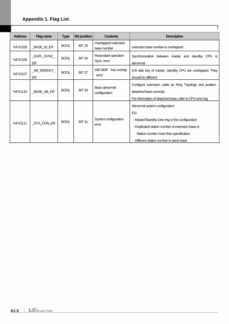
Appendix 1. Flag List
A1-3
Address Flag name Type Bit position Contents Description
%FX2105 _BASE_ID_ER BOOL BIT 25 Overlapped extension base number extension base number is overlapped
%FX2106 _DUPL_SYNC_
ER BOOL BIT 26
Redundant operation Sync. error
Synchronization between master and standby CPU is
abnormal
%FX2107 _AB_SIDEKEY_
ER BOOL BIT 27
A/B SIDE key overlap error
A,B side key of master, standby CPU are overlapped. They
should be different.
%FX2110 _BASE_AB_ER BOOL BIT 30 Base abnormal configuration
Configure extension cable as Ring Topology and position
detached base correctly.
For information of detached base, refer to CPU error log
%FX2111 _SYS_CON_ER BOOL BIT 31 System configuration error
Abnormal system configuration
Ex)
- Master/Standby One ring or line configuration
- Duplicated station number of extension base or
Station number more than specification
- Different station number in same base
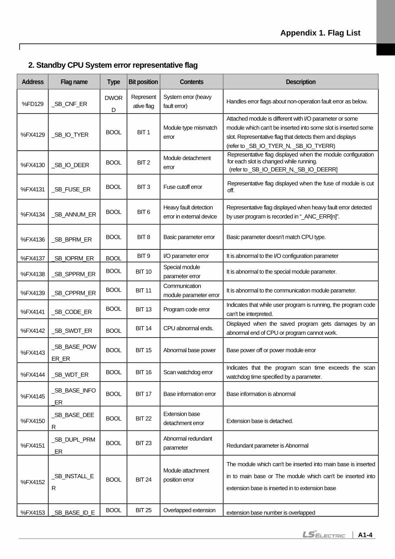
Appendix 1. Flag List
A1-4
2. Standby CPU System error representative flag
Address Flag name Type Bit position Contents Description
%FD129 _SB_CNF_ER DWOR
D
Representative flag
System error (heavy fault error)
Handles error flags about non-operation fault error as below.
%FX4129 _SB_IO_TYER BOOL BIT 1 Module type mismatch error
Attached module is different with I/O parameter or some module which can’t be inserted into some slot is inserted some slot. Representative flag that detects them and displays (refer to _SB_IO_TYER_N, _SB_IO_TYERR)
%FX4130 _SB_IO_DEER BOOL BIT 2 Module detachment error
Representative flag displayed when the module configuration for each slot is changed while running. (refer to _SB_IO_DEER_N,_SB_IO_DEERR]
%FX4131 _SB_FUSE_ER BOOL BIT 3 Fuse cutoff error Representative flag displayed when the fuse of module is cut off.
%FX4134 _SB_ANNUM_ER BOOL BIT 6 Heavy fault detection error in external device
Representative flag displayed when heavy fault error detected by user program is recorded in “_ANC_ERR[n]”.
%FX4136 _SB_BPRM_ER BOOL BIT 8 Basic parameter error Basic parameter doesn’t match CPU type.
%FX4137 _SB_IOPRM_ER BOOL BIT 9 I/O parameter error It is abnormal to the I/O configuration parameter
%FX4138 _SB_SPPRM_ER BOOL BIT 10 Special module parameter error
It is abnormal to the special module parameter.
%FX4139 _SB_CPPRM_ER BOOL BIT 11 Communication module parameter error
It is abnormal to the communication module parameter.
%FX4141 _SB_CODE_ER BOOL BIT 13 Program code error Indicates that while user program is running, the program code can’t be interpreted.
%FX4142 _SB_SWDT_ER BOOL BIT 14 CPU abnormal ends. Displayed when the saved program gets damages by an abnormal end of CPU or program cannot work.
%FX4143 _SB_BASE_POW
ER_ER BOOL BIT 15 Abnormal base power Base power off or power module error
%FX4144 _SB_WDT_ER BOOL BIT 16 Scan watchdog error Indicates that the program scan time exceeds the scan watchdog time specified by a parameter.
%FX4145 _SB_BASE_INFO
_ER BOOL BIT 17 Base information error Base information is abnormal
%FX4150 _SB_BASE_DEE
R BOOL BIT 22
Extension base detachment error Extension base is detached.
%FX4151 _SB_DUPL_PRM
_ER BOOL BIT 23
Abnormal redundant parameter Redundant parameter is Abnormal
%FX4152 _SB_INSTALL_E
R BOOL BIT 24
Module attachment position error
The module which can’t be inserted into main base is inserted
in to main base or The module which can’t be inserted into
extension base is inserted in to extension base
%FX4153 _SB_BASE_ID_E BOOL BIT 25 Overlapped extension extension base number is overlapped
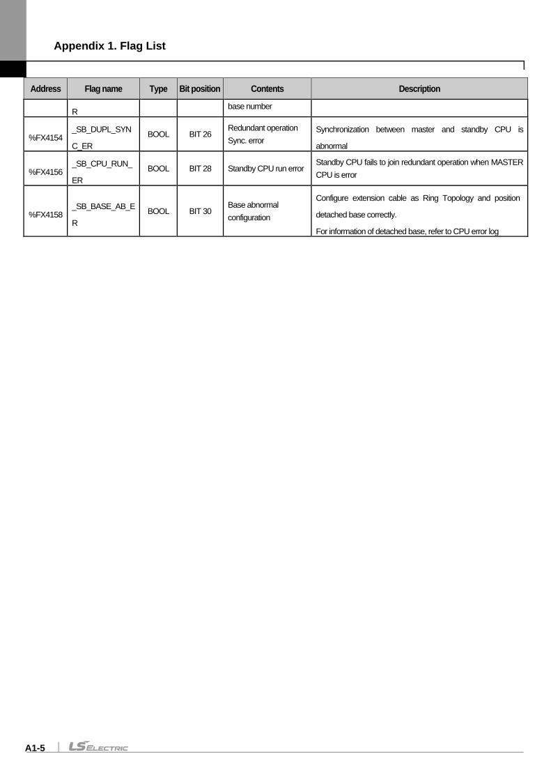
Appendix 1. Flag List
A1-5
Address Flag name Type Bit position Contents Description
R base number
%FX4154 _SB_DUPL_SYN
C_ER BOOL BIT 26
Redundant operation Sync. error
Synchronization between master and standby CPU is
abnormal
%FX4156 _SB_CPU_RUN_
ER BOOL BIT 28 Standby CPU run error
Standby CPU fails to join redundant operation when MASTER CPU is error
%FX4158 _SB_BASE_AB_E
R BOOL BIT 30
Base abnormal configuration
Configure extension cable as Ring Topology and position
detached base correctly.
For information of detached base, refer to CPU error log
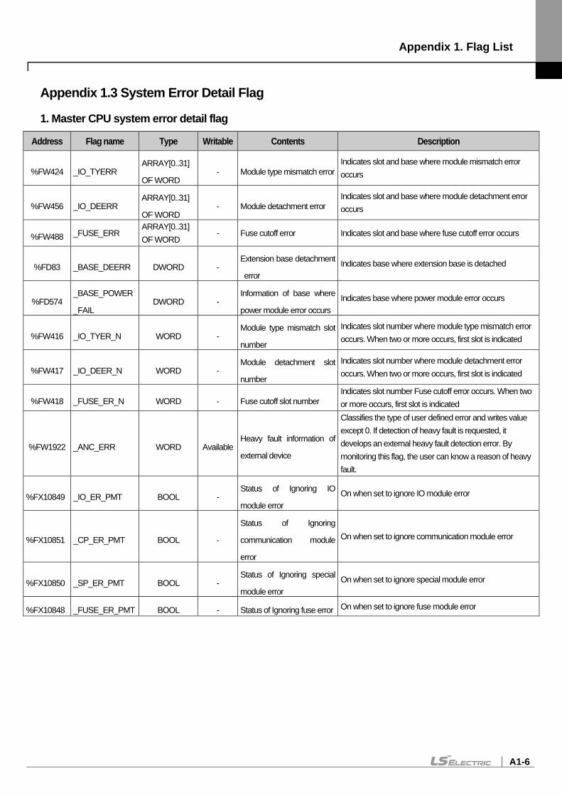
Appendix 1. Flag List
A1-6
Appendix 1.3 System Error Detail Flag
1. Master CPU system error detail flag
Address Flag name Type Writable Contents Description
%FW424 _IO_TYERR ARRAY[0..31]
OF WORD - Module type mismatch error
Indicates slot and base where module mismatch error occurs
%FW456 _IO_DEERR ARRAY[0..31]
OF WORD - Module detachment error
Indicates slot and base where module detachment error occurs
%FW488 _FUSE_ERR ARRAY[0..31] OF WORD
- Fuse cutoff error Indicates slot and base where fuse cutoff error occurs
%FD83 _BASE_DEERR DWORD - Extension base detachment
error Indicates base where extension base is detached
%FD574 _BASE_POWER
_FAIL DWORD -
Information of base where
power module error occurs Indicates base where power module error occurs
%FW416 _IO_TYER_N WORD - Module type mismatch slot
number
Indicates slot number where module type mismatch error occurs. When two or more occurs, first slot is indicated
%FW417 _IO_DEER_N WORD - Module detachment slot
number
Indicates slot number where module detachment error occurs. When two or more occurs, first slot is indicated
%FW418 _FUSE_ER_N WORD - Fuse cutoff slot number Indicates slot number Fuse cutoff error occurs. When two or more occurs, first slot is indicated
%FW1922 _ANC_ERR WORD Available Heavy fault information of
external device
Classifies the type of user defined error and writes value except 0. If detection of heavy fault is requested, it develops an external heavy fault detection error. By monitoring this flag, the user can know a reason of heavy fault.
%FX10849 _IO_ER_PMT BOOL - Status of Ignoring IO
module error On when set to ignore IO module error
%FX10851 _CP_ER_PMT BOOL -
Status of Ignoring
communication module
error
On when set to ignore communication module error
%FX10850 _SP_ER_PMT BOOL - Status of Ignoring special
module error On when set to ignore special module error
%FX10848 _FUSE_ER_PMT BOOL - Status of Ignoring fuse error On when set to ignore fuse module error
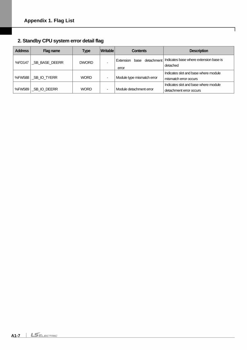
Appendix 1. Flag List
A1-7
2. Standby CPU system error detail flag
Address Flag name Type Writable Contents Description
%FD147 _SB_BASE_DEERR DWORD - Extension base detachment
error
Indicates base where extension base is detached
%FW588 _SB_IO_TYERR WORD - Module type mismatch error Indicates slot and base where module mismatch error occurs
%FW589 _SB_IO_DEERR WORD - Module detachment error Indicates slot and base where module detachment error occurs
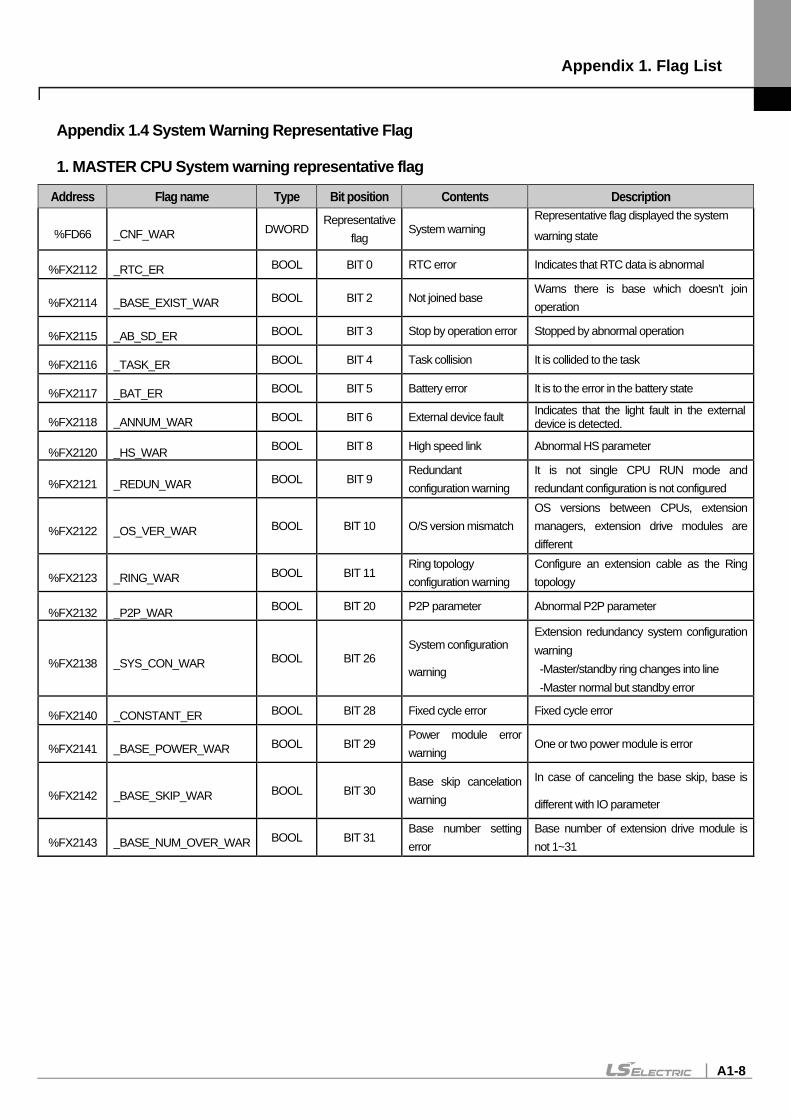
Appendix 1. Flag List
A1-8
Appendix 1.4 System Warning Representative Flag
1. MASTER CPU System warning representative flag
Address Flag name Type Bit position Contents Description
%FD66 _CNF_WAR DWORD Representative
flag System warning
Representative flag displayed the system
warning state
%FX2112 _RTC_ER BOOL BIT 0 RTC error Indicates that RTC data is abnormal
%FX2114 _BASE_EXIST_WAR BOOL BIT 2 Not joined base Warns there is base which doesn’t join operation
%FX2115 _AB_SD_ER BOOL BIT 3 Stop by operation error Stopped by abnormal operation
%FX2116 _TASK_ER BOOL BIT 4 Task collision It is collided to the task
%FX2117 _BAT_ER BOOL BIT 5 Battery error It is to the error in the battery state
%FX2118 _ANNUM_WAR BOOL BIT 6 External device fault Indicates that the light fault in the external device is detected.
%FX2120 _HS_WAR BOOL BIT 8 High speed link Abnormal HS parameter
%FX2121 _REDUN_WAR BOOL BIT 9 Redundant configuration warning
It is not single CPU RUN mode and redundant configuration is not configured
%FX2122 _OS_VER_WAR BOOL BIT 10 O/S version mismatch OS versions between CPUs, extension managers, extension drive modules are different
%FX2123 _RING_WAR BOOL BIT 11 Ring topology configuration warning
Configure an extension cable as the Ring topology
%FX2132 _P2P_WAR BOOL BIT 20 P2P parameter Abnormal P2P parameter
%FX2138 _SYS_CON_WAR BOOL BIT 26 System configuration
warning
Extension redundancy system configuration warning -Master/standby ring changes into line -Master normal but standby error
%FX2140 _CONSTANT_ER BOOL BIT 28 Fixed cycle error Fixed cycle error
%FX2141 _BASE_POWER_WAR BOOL BIT 29 Power module error warning
One or two power module is error
%FX2142 _BASE_SKIP_WAR BOOL BIT 30 Base skip cancelation warning
In case of canceling the base skip, base is
different with IO parameter
%FX2143 _BASE_NUM_OVER_WAR BOOL BIT 31 Base number setting error
Base number of extension drive module is not 1~31
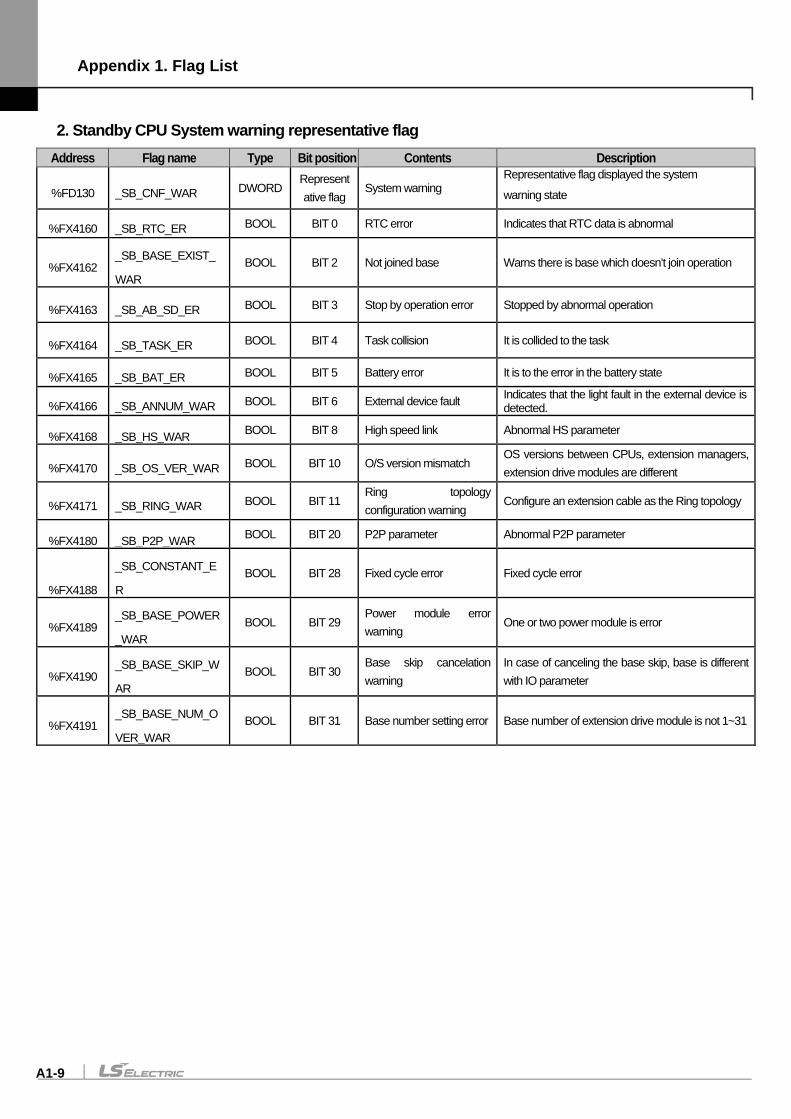
Appendix 1. Flag List
A1-9
2. Standby CPU System warning representative flag Address Flag name Type Bit position Contents Description
%FD130 _SB_CNF_WAR DWORD Representative flag
System warning Representative flag displayed the system
warning state
%FX4160 _SB_RTC_ER BOOL BIT 0 RTC error Indicates that RTC data is abnormal
%FX4162 _SB_BASE_EXIST_
WAR BOOL BIT 2 Not joined base Warns there is base which doesn’t join operation
%FX4163 _SB_AB_SD_ER BOOL BIT 3 Stop by operation error Stopped by abnormal operation
%FX4164 _SB_TASK_ER BOOL BIT 4 Task collision It is collided to the task
%FX4165 _SB_BAT_ER BOOL BIT 5 Battery error It is to the error in the battery state
%FX4166 _SB_ANNUM_WAR BOOL BIT 6 External device fault Indicates that the light fault in the external device is detected.
%FX4168 _SB_HS_WAR BOOL BIT 8 High speed link Abnormal HS parameter
%FX4170 _SB_OS_VER_WAR BOOL BIT 10 O/S version mismatch OS versions between CPUs, extension managers, extension drive modules are different
%FX4171 _SB_RING_WAR BOOL BIT 11 Ring topology configuration warning
Configure an extension cable as the Ring topology
%FX4180 _SB_P2P_WAR BOOL BIT 20 P2P parameter Abnormal P2P parameter
%FX4188
_SB_CONSTANT_E
R BOOL BIT 28 Fixed cycle error Fixed cycle error
%FX4189 _SB_BASE_POWER
_WAR BOOL BIT 29
Power module error warning
One or two power module is error
%FX4190 _SB_BASE_SKIP_W
AR BOOL BIT 30
Base skip cancelation warning
In case of canceling the base skip, base is different with IO parameter
%FX4191 _SB_BASE_NUM_O
VER_WAR BOOL BIT 31 Base number setting error Base number of extension drive module is not 1~31
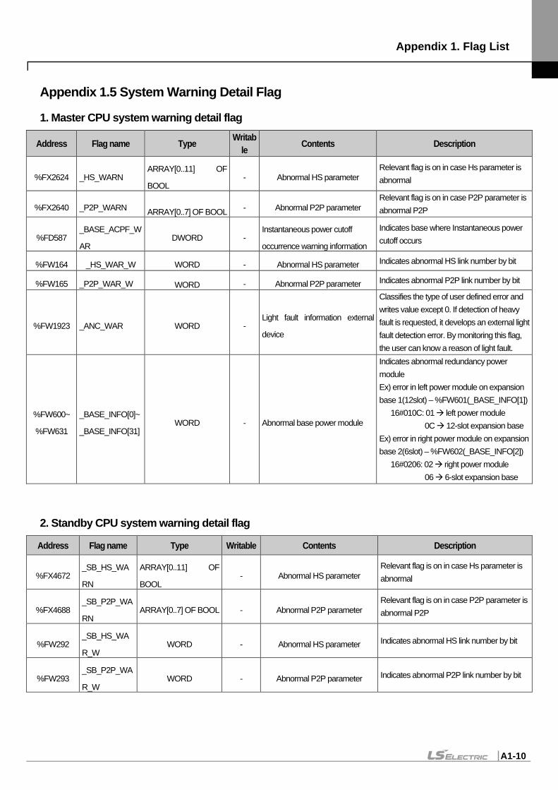
Appendix 1. Flag List
A1-10
Appendix 1.5 System Warning Detail Flag
1. Master CPU system warning detail flag
Address Flag name Type Writable Contents Description
%FX2624 _HS_WARN ARRAY[0..11] OF
BOOL - Abnormal HS parameter
Relevant flag is on in case Hs parameter is abnormal
%FX2640 _P2P_WARN ARRAY[0..7] OF BOOL - Abnormal P2P parameter Relevant flag is on in case P2P parameter is abnormal P2P
%FD587 _BASE_ACPF_W
AR DWORD -
Instantaneous power cutoff
occurrence warning information
Indicates base where Instantaneous power cutoff occurs
%FW164 _HS_WAR_W WORD - Abnormal HS parameter Indicates abnormal HS link number by bit
%FW165 _P2P_WAR_W WORD - Abnormal P2P parameter Indicates abnormal P2P link number by bit
%FW1923 _ANC_WAR WORD - Light fault information external
device
Classifies the type of user defined error and writes value except 0. If detection of heavy fault is requested, it develops an external light fault detection error. By monitoring this flag, the user can know a reason of light fault.
%FW600~
%FW631
_BASE_INFO[0]~
_BASE_INFO[31] WORD - Abnormal base power module
Indicates abnormal redundancy power module Ex) error in left power module on expansion base 1(12slot) – %FW601(_BASE_INFO[1]) 16#010C: 01 left power module 0C 12-slot expansion base Ex) error in right power module on expansion base 2(6slot) – %FW602(_BASE_INFO[2]) 16#0206: 02 right power module 06 6-slot expansion base
2. Standby CPU system warning detail flag
Address Flag name Type Writable Contents Description
%FX4672 _SB_HS_WA
RN
ARRAY[0..11] OF
BOOL - Abnormal HS parameter
Relevant flag is on in case Hs parameter is abnormal
%FX4688 _SB_P2P_WA
RN ARRAY[0..7] OF BOOL - Abnormal P2P parameter
Relevant flag is on in case P2P parameter is abnormal P2P
%FW292 _SB_HS_WA
R_W WORD - Abnormal HS parameter Indicates abnormal HS link number by bit
%FW293 _SB_P2P_WA
R_W WORD - Abnormal P2P parameter Indicates abnormal P2P link number by bit
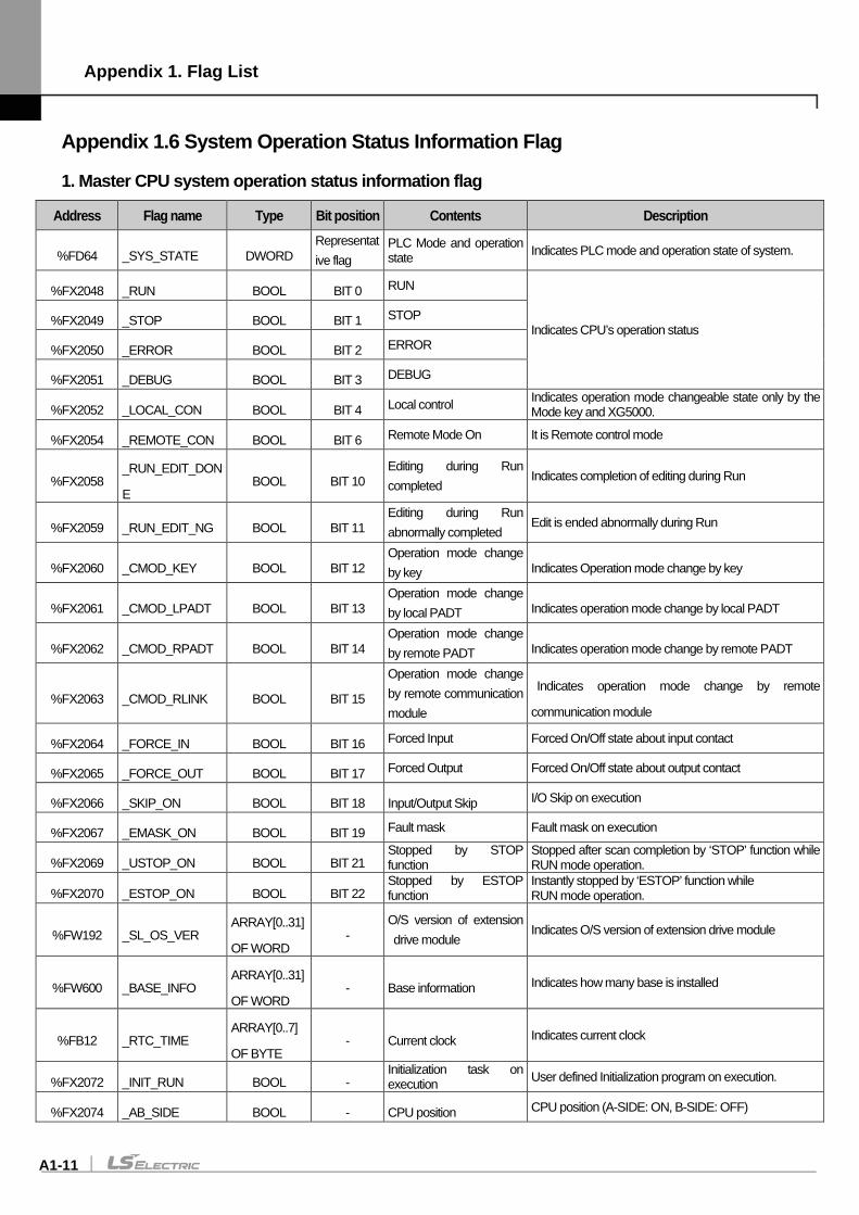
Appendix 1. Flag List
A1-11
Appendix 1.6 System Operation Status Information Flag
1. Master CPU system operation status information flag
Address Flag name Type Bit position Contents Description
%FD64 _SYS_STATE DWORD Representative flag
PLC Mode and operation state Indicates PLC mode and operation state of system.
%FX2048 _RUN BOOL BIT 0 RUN
Indicates CPU’s operation status %FX2049 _STOP BOOL BIT 1 STOP
%FX2050 _ERROR BOOL BIT 2 ERROR
%FX2051 _DEBUG BOOL BIT 3 DEBUG
%FX2052 _LOCAL_CON BOOL BIT 4 Local control Indicates operation mode changeable state only by the Mode key and XG5000.
%FX2054 _REMOTE_CON BOOL BIT 6 Remote Mode On It is Remote control mode
%FX2058 _RUN_EDIT_DON
E BOOL BIT 10
Editing during Run completed
Indicates completion of editing during Run
%FX2059 _RUN_EDIT_NG BOOL BIT 11 Editing during Run abnormally completed
Edit is ended abnormally during Run
%FX2060 _CMOD_KEY BOOL BIT 12 Operation mode change by key Indicates Operation mode change by key
%FX2061 _CMOD_LPADT BOOL BIT 13 Operation mode change by local PADT Indicates operation mode change by local PADT
%FX2062 _CMOD_RPADT BOOL BIT 14 Operation mode change by remote PADT Indicates operation mode change by remote PADT
%FX2063 _CMOD_RLINK BOOL BIT 15
Operation mode change by remote communication module
Indicates operation mode change by remote
communication module
%FX2064 _FORCE_IN BOOL BIT 16 Forced Input Forced On/Off state about input contact
%FX2065 _FORCE_OUT BOOL BIT 17 Forced Output Forced On/Off state about output contact
%FX2066 _SKIP_ON BOOL BIT 18 Input/Output Skip I/O Skip on execution
%FX2067 _EMASK_ON BOOL BIT 19 Fault mask Fault mask on execution
%FX2069 _USTOP_ON BOOL BIT 21 Stopped by STOP function
Stopped after scan completion by ‘STOP’ function while RUN mode operation.
%FX2070 _ESTOP_ON BOOL BIT 22 Stopped by ESTOP function
Instantly stopped by ‘ESTOP’ function while RUN mode operation.
%FW192 _SL_OS_VER ARRAY[0..31]
OF WORD -
O/S version of extension drive module
Indicates O/S version of extension drive module
%FW600 _BASE_INFO ARRAY[0..31]
OF WORD - Base information Indicates how many base is installed
%FB12 _RTC_TIME ARRAY[0..7]
OF BYTE - Current clock Indicates current clock
%FX2072 _INIT_RUN BOOL - Initialization task on execution User defined Initialization program on execution.
%FX2074 _AB_SIDE BOOL - CPU position CPU position (A-SIDE: ON, B-SIDE: OFF)
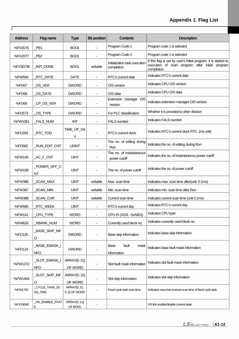
Appendix 1. Flag List
A1-12
Address Flag name Type Bit position Contents Description
%FX2076 _PB1 BOOL - Program Code 1 Program code 1 is selected
%FX2077 _PB2 BOOL - Program Code 2 Program code 1 is selected
%FX30736 _INIT_DONE BOOL writable Initialization task execution completion
If this flag is set by user’s initial program, it is started to execution of scan program after initial program completion.
%FW584 _RTC_DATE DATE - RTC’s current date Indicates RTC’s current date
%FD67 _OS_VER DWORD - O/S version Indicates CPU O/S version
%FD68 _OS_DATE DWORD - O/S data Indicates CPU O/S data
%FD69 _CP_OS_VER DWORD - Extension manager O/S version
Indicates extension manager O/S version
%FD573 _OS_TYPE DWORD - For PLC classification Whether it is provided to other division
%FW1081 _FALS_NUM INT - FALS number Indicates FALS number
%FD293 _RTC_TOD TIME_OF_DA
Y - RTC’s current clock Indicates RTC’s current clock RTC. (ms unit)
%FD582 _RUN_EDIT_CNT UDINT - The no. of editing during Run
Indicates the no. of editing during Run
%FW140 _AC_F_CNT UINT - The no. of instantaneous power cutoff
Indicates the no. of instantaneous power cutoff
%FW158 _POWER_OFF_C
NT UINT - The no. of power cutoff Indicates the no. of power cutoff
%FW386 _SCAN_MAX UINT writable Max. scan time Indicates max. scan time after(unit: 0.1ms)
%FW387 _SCAN_MIN UINT writable Min. scan time Indicates min. scan time after Run
%FW388 _SCAN_CUR UINT writable Current scan time Indicates current scan time (unit 0.1ms)
%FW585 _RTC_WEEK UINT - RTC’s current day Indicates RTC’s current day
%FW141 _CPU_TYPE WORD - CPU ID (XGR - 0xA801) Indicates CPU type
%FW633 _RBANK_NUM WORD - Currently used block no. Indicates currently used block no.
%FD125 _BASE_SKIP_INF
O DWORD - Base skip information Indicates base skip information
%FD124 _BASE_EMASK_I
NFO DWORD -
Base fault mask
information Indicates base fault mask information
%FW1372 _SLOT_EMASK_I
NFO
ARRAY[0..31]
OF WORD - Slot fault mask information Indicates slot fault mask information
%FW1404 _SLOT_SKIP_INF
O
ARRAY[0..31]
OF WORD - Slot skip information Indicates slot skip information
%FW1752
_CYCLE_TASK_SCAN_TIME
ARRAY[0..31, 0..2] OF WORD
-
Fixed cycle task scan time
Indicates max./min./current scan time of fixed cycle task
%FX19040 _HS_ENABLE_STATE
ARRAY[0..11] OF BOOL
- - HS link enable/disable current state
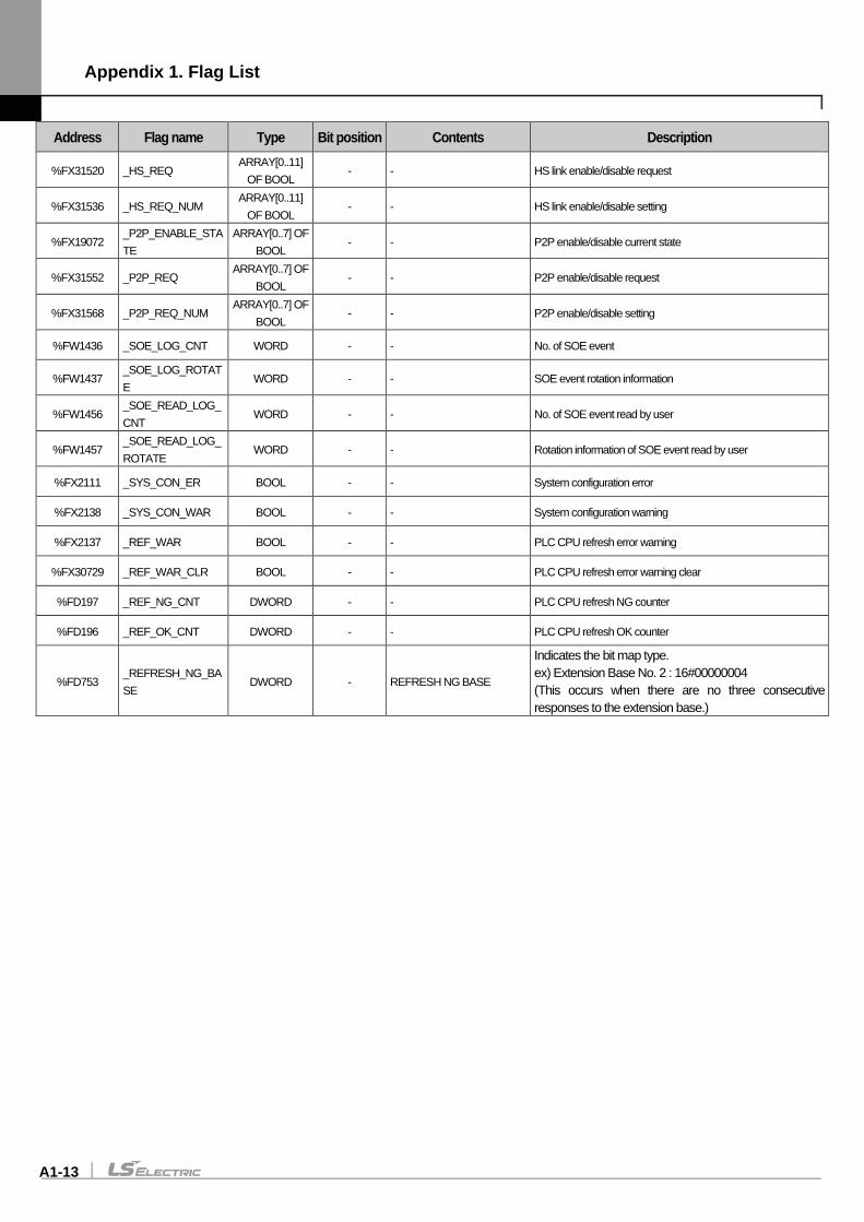
Appendix 1. Flag List
A1-13
Address Flag name Type Bit position Contents Description
%FX31520 _HS_REQ ARRAY[0..11]
OF BOOL - - HS link enable/disable request
%FX31536 _HS_REQ_NUM ARRAY[0..11]
OF BOOL - - HS link enable/disable setting
%FX19072 _P2P_ENABLE_STATE
ARRAY[0..7] OF BOOL
- - P2P enable/disable current state
%FX31552 _P2P_REQ ARRAY[0..7] OF
BOOL - - P2P enable/disable request
%FX31568 _P2P_REQ_NUM ARRAY[0..7] OF
BOOL - - P2P enable/disable setting
%FW1436 _SOE_LOG_CNT WORD - - No. of SOE event
%FW1437 _SOE_LOG_ROTATE
WORD - - SOE event rotation information
%FW1456 _SOE_READ_LOG_CNT
WORD - - No. of SOE event read by user
%FW1457 _SOE_READ_LOG_ROTATE
WORD - - Rotation information of SOE event read by user
%FX2111 _SYS_CON_ER BOOL - - System configuration error
%FX2138 _SYS_CON_WAR BOOL - - System configuration warning
%FX2137 _REF_WAR BOOL - - PLC CPU refresh error warning
%FX30729 _REF_WAR_CLR BOOL - - PLC CPU refresh error warning clear
%FD197 _REF_NG_CNT DWORD - - PLC CPU refresh NG counter
%FD196 _REF_OK_CNT DWORD - - PLC CPU refresh OK counter
%FD753 _REFRESH_NG_BASE
DWORD - REFRESH NG BASE
Indicates the bit map type. ex) Extension Base No. 2 : 16#00000004 (This occurs when there are no three consecutive responses to the extension base.)
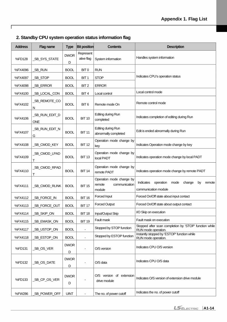
Appendix 1. Flag List
A1-14
2. Standby CPU system operation status information flag
Address Flag name Type Bit position Contents Description
%FD128 _SB_SYS_STATE DWOR
D
Representative flag System information Handles system information
%FX4096 _SB_RUN BOOL BIT 0 RUN
Indicates CPU’s operation status %FX4097 _SB_STOP BOOL BIT 1 STOP
%FX4098 _SB_ERROR BOOL BIT 2 ERROR
%FX4100 _SB_LOCAL_CON BOOL BIT 4 Local control Local control mode
%FX4102 _SB_REMOTE_CO
N BOOL BIT 6 Remote mode On Remote control mode
%FX4106 _SB_RUN_EDIT_D
ONE BOOL BIT 10
Editing during Run completed
Indicates completion of editing during Run
%FX4107 _SB_RUN_EDIT_N
G BOOL BIT 11
Editing during Run abnormally completed
Edit is ended abnormally during Run
%FX4108 _SB_CMOD_KEY BOOL BIT 12 Operation mode change by key Indicates Operation mode change by key
%FX4109 _SB_CMOD_LPAD
T BOOL BIT 13
Operation mode change by local PADT Indicates operation mode change by local PADT
%FX4110 _SB_CMOD_RPAD
T BOOL BIT 14
Operation mode change by remote PADT Indicates operation mode change by remote PADT
%FX4111 _SB_CMOD_RLINK BOOL BIT 15
Operation mode change by remote communication module
Indicates operation mode change by remote
communication module
%FX4112 _SB_FORCE_IN BOOL BIT 16 Forced Input Forced On/Off state about input contact
%FX4113 _SB_FORCE_OUT BOOL BIT 17 Forced Output Forced On/Off state about output contact
%FX4114 _SB_SKIP_ON BOOL BIT 18 Input/Output Skip I/O Skip on execution
%FX4115 _SB_EMASK_ON BOOL BIT 19 Fault mask Fault mask on execution
%FX4117 _SB_USTOP_ON BOOL - Stopped by STOP function Stopped after scan completion by ‘STOP’ function while RUN mode operation.
%FX4118 _SB_ESTOP_ON BOOL - Stopped by ESTOP function Instantly stopped by ‘ESTOP’ function while RUN mode operation.
%FD131 _SB_OS_VER DWOR
D - O/S version Indicates CPU O/S version
%FD132 _SB_OS_DATE DWOR
D - O/S data Indicates CPU O/S data
%FD133 _SB_CP_OS_VER DWOR
D -
O/S version of extension drive module
Indicates O/S version of extension drive module
%FW286 _SB_POWER_OFF UINT - The no. of power cutoff Indicates the no. of power cutoff

Appendix 1. Flag List
A1-15
Address Flag name Type Bit position Contents Description
_CNT
%FW269 _SB_CPU_TYPE WORD - CPU ID (XGR - 0xA801) Indicates CPU type
%FW632 _SB_BASE_INFO WORD - Base information Indicates how many base is installed.
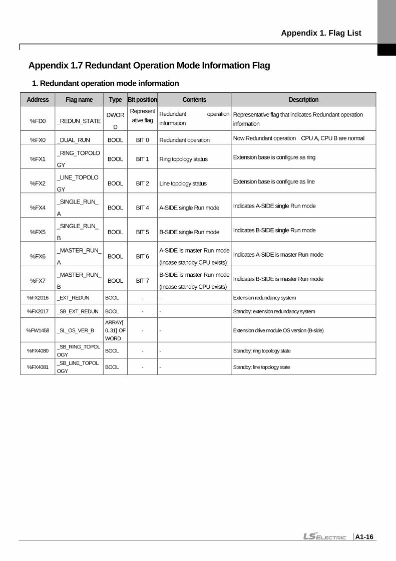
Appendix 1. Flag List
A1-16
Appendix 1.7 Redundant Operation Mode Information Flag
1. Redundant operation mode information
Address Flag name Type Bit position Contents Description
%FD0 _REDUN_STATE DWOR
D
Representative flag
Redundant operation information
Representative flag that indicates Redundant operation information
%FX0 _DUAL_RUN BOOL BIT 0 Redundant operation Now Redundant operation CPU A, CPU B are normal
%FX1 _RING_TOPOLO
GY BOOL BIT 1 Ring topology status Extension base is configure as ring
%FX2 _LINE_TOPOLO
GY BOOL BIT 2 Line topology status Extension base is configure as line
%FX4 _SINGLE_RUN_
A BOOL BIT 4 A-SIDE single Run mode Indicates A-SIDE single Run mode
%FX5 _SINGLE_RUN_
B BOOL BIT 5 B-SIDE single Run mode Indicates B-SIDE single Run mode
%FX6 _MASTER_RUN_
A BOOL BIT 6
A-SIDE is master Run mode
(Incase standby CPU exists) Indicates A-SIDE is master Run mode
%FX7 _MASTER_RUN_
B BOOL BIT 7
B-SIDE is master Run mode
(Incase standby CPU exists) Indicates B-SIDE is master Run mode
%FX2016 _EXT_REDUN BOOL - - Extension redundancy system
%FX2017 _SB_EXT_REDUN BOOL - - Standby: extension redundancy system
%FW1458 _SL_OS_VER_B ARRAY[0..31] OF WORD
- - Extension drive module OS version (B-side)
%FX4080 _SB_RING_TOPOLOGY
BOOL - - Standby: ring topology state
%FX4081 _SB_LINE_TOPOLOGY
BOOL - - Standby: line topology state
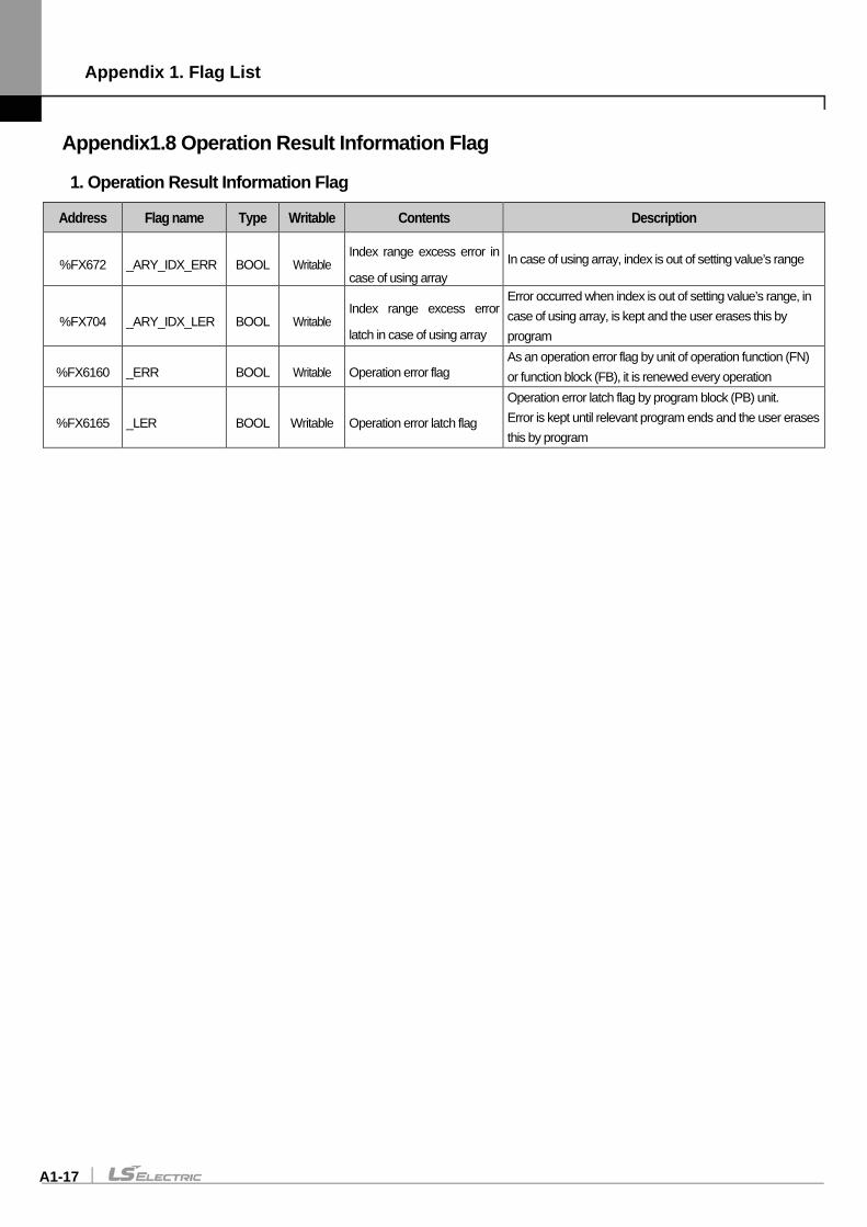
Appendix 1. Flag List
A1-17
Appendix1.8 Operation Result Information Flag
1. Operation Result Information Flag
Address Flag name Type Writable Contents Description
%FX672 _ARY_IDX_ERR BOOL Writable Index range excess error in
case of using array In case of using array, index is out of setting value’s range
%FX704 _ARY_IDX_LER BOOL Writable Index range excess error
latch in case of using array
Error occurred when index is out of setting value’s range, in case of using array, is kept and the user erases this by program
%FX6160 _ERR BOOL Writable Operation error flag As an operation error flag by unit of operation function (FN) or function block (FB), it is renewed every operation
%FX6165 _LER BOOL Writable Operation error latch flag
Operation error latch flag by program block (PB) unit. Error is kept until relevant program ends and the user erases this by program
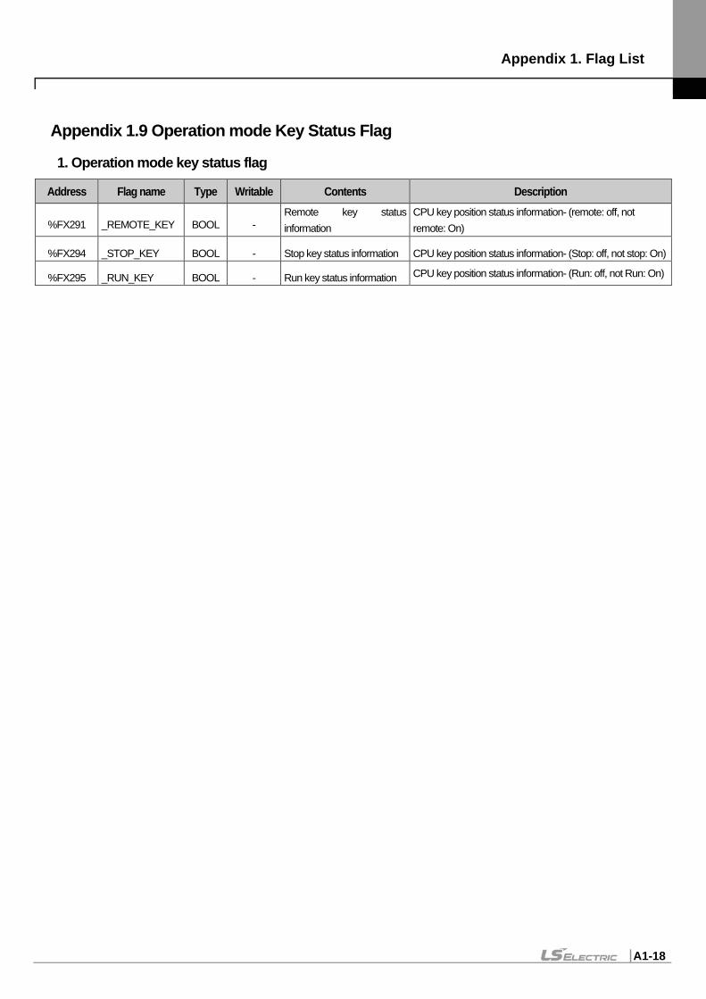
Appendix 1. Flag List
A1-18
Appendix 1.9 Operation mode Key Status Flag
1. Operation mode key status flag
Address Flag name Type Writable Contents Description
%FX291 _REMOTE_KEY BOOL - Remote key status information
CPU key position status information- (remote: off, not remote: On)
%FX294 _STOP_KEY BOOL - Stop key status information CPU key position status information- (Stop: off, not stop: On)
%FX295 _RUN_KEY BOOL - Run key status information CPU key position status information- (Run: off, not Run: On)
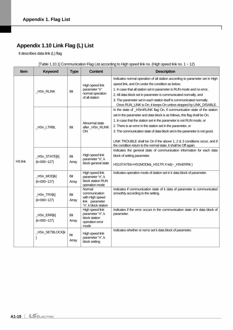
Appendix 1. Flag List
A1-19
Appendix 1.10 Link Flag (L) List It describes data link (L) flag
[Table 1.10.1] Communication Flag List according to High speed link no. (High speed link no. 1 ~ 12)
Item Keyword Type Content Description
HS link
_HSn_RLINK Bit
High speed link parameter “n” normal operation of all station
Indicates normal operation of all station according to parameter set in High speed link, and On under the condition as below. 1. In case that all station set in parameter is RUN mode and no error, 2. All data block set in parameter is communicated normally, and 3. The parameter set in each station itself is communicated normally.
Once RUN_LINK is On, it keeps On unless stopped by LINK_DISABLE.
_HSn_LTRBL Bit Abnormal state after _HSn_RLINK ON
In the state of _HSmRLINK flag On, if communication state of the station set in the parameter and data block is as follows, this flag shall be On. 1. In case that the station set in the parameter is not RUN mode, or 2. There is an error in the station set in the parameter, or 3. The communication state of data block set in the parameter is not good. LINK TROUBLE shall be On if the above 1, 2 & 3 conditions occur, and if the condition return to the normal state, it shall be Off again.
_HSn_STATE[k] (k=000~127)
Bit Array
High speed link parameter “n”, k block general state
Indicates the general state of communication information for each data block of setting parameter. HS1STATEk=HS1MODk&_HS1TR X k&(~_HSnERRk )
_HSn_MOD[k] (k=000~127)
Bit Array
High speed link parameter “n”, k block station RUN operation mode
Indicates operation mode of station set in k data block of parameter.
_HSn_TRX[k] (k=000~127)
Bit Array
Normal communication with High speed link parameter “n”, k block station
Indicates if communication state of k data of parameter is communicated smoothly according to the setting.
_HSn_ERR[k] (k=000~127)
Bit Array
High speed link parameter “n”, k block station operation error mode
Indicates if the error occurs in the communication state of k data block of parameter.
_HSn_SETBLOCK[k]
bit Array
High speed link parameter “n”, k block setting
Indicates whether or not to set k data block of parameter.
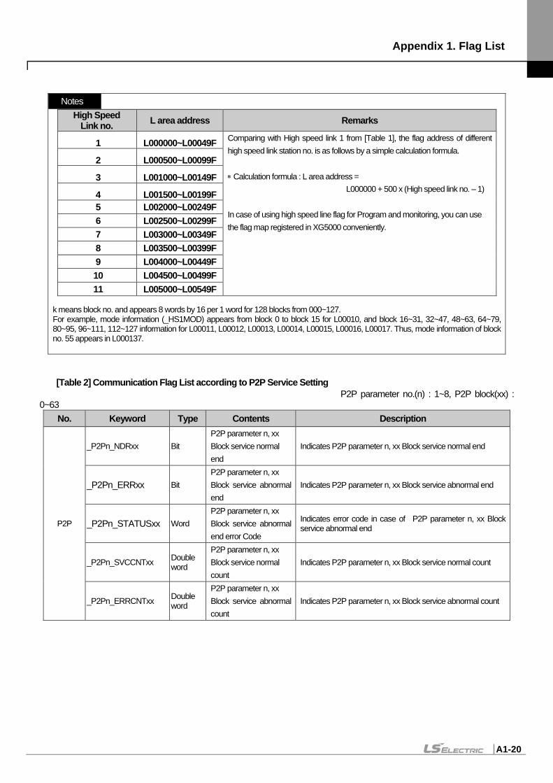
Appendix 1. Flag List
A1-20
[Table 2] Communication Flag List according to P2P Service Setting P2P parameter no.(n) : 1~8, P2P block(xx) :
0~63 No. Keyword Type Contents Description
P2P
_P2Pn_NDRxx Bit P2P parameter n, xx Block service normal end
Indicates P2P parameter n, xx Block service normal end
_P2Pn_ERRxx Bit P2P parameter n, xx Block service abnormal end
Indicates P2P parameter n, xx Block service abnormal end
_P2Pn_STATUSxx Word P2P parameter n, xx Block service abnormal end error Code
Indicates error code in case of P2P parameter n, xx Block service abnormal end
_P2Pn_SVCCNTxx Double word
P2P parameter n, xx Block service normal count
Indicates P2P parameter n, xx Block service normal count
_P2Pn_ERRCNTxx Double word
P2P parameter n, xx Block service abnormal count
Indicates P2P parameter n, xx Block service abnormal count
Notes High Speed
Link no. L area address Remarks
1 L000000~L00049F Comparing with High speed link 1 from [Table 1], the flag address of different high speed link station no. is as follows by a simple calculation formula. ∗ Calculation formula : L area address =
L000000 + 500 x (High speed link no. – 1) In case of using high speed line flag for Program and monitoring, you can use the flag map registered in XG5000 conveniently.
2 L000500~L00099F
3 L001000~L00149F
4 L001500~L00199F 5 L002000~L00249F 6 L002500~L00299F 7 L003000~L00349F 8 L003500~L00399F 9 L004000~L00449F 10 L004500~L00499F 11 L005000~L00549F
k means block no. and appears 8 words by 16 per 1 word for 128 blocks from 000~127. For example, mode information (_HS1MOD) appears from block 0 to block 15 for L00010, and block 16~31, 32~47, 48~63, 64~79, 80~95, 96~111, 112~127 information for L00011, L00012, L00013, L00014, L00015, L00016, L00017. Thus, mode information of block no. 55 appears in L000137.
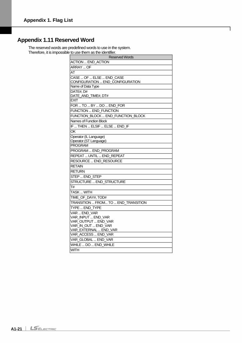
Appendix 1. Flag List
A1-21
Appendix 1.11 Reserved Word The reserved words are predefined words to use in the system. Therefore, it is impossible to use them as the identifier.
Reserved Words ACTION ... END_ACTION ARRAY ... OF AT CASE ... OF ... ELSE ... END_CASE CONFIGURATION ... END_CONFIGURATION Name of Data Type DATE#, D# DATE_AND_TIME#, DT# EXIT FOR ... TO ... BY ... DO ... END_FOR FUNCTION ... END_FUNCTION FUNCTION_BLOCK ... END_FUNCTION_BLOCK Names of Function Block IF ... THEN ... ELSIF ... ELSE ... END_IF OK Operator (IL Language) Operator (ST Language) PROGRAM PROGRAM ... END_PROGRAM REPEAT ... UNTIL ... END_REPEAT RESOURCE ... END_RESOURCE RETAIN RETURN STEP ... END_STEP STRUCTURE ... END_STRUCTURE T# TASK ... WITH TIME_OF_DAY#, TOD# TRANSITION ... FROM... TO ... END_TRANSITION TYPE ... END_TYPE VAR ... END_VAR VAR_INPUT ... END_VAR VAR_OUTPUT ... END_VAR VAR_IN_OUT ... END_VAR VAR_EXTERNAL ... END_VAR VAR_ACCESS ... END_VAR VAR_GLOBAL ... END_VAR WHILE ... DO ... END_WHILE WITH

Appendix 1. Flag List
A1-22
Warranty and Environmental Policy
1
Warranty 1. Warranty Period
The product you purchased will be guaranteed for 18 months from the date of manufacturing. 2. Scope of Warranty Any trouble or defect occurring for the above-mentioned period will be partially replaced or repaired. However, please note the
following cases will be excluded from the scope of warranty.
(1) Any trouble attributable to unreasonable condition, environment or handling otherwise specified in the manual, (2) Any trouble attributable to others’ products, (3) If the product is modified or repaired in any other place not designated by the company, (4) Due to unintended purposes (5) Owing to the reasons unexpected at the level of the contemporary science and technology when delivered. (6) Not attributable to the company; for instance, natural disasters or fire
3. Since the above warranty is limited to PLC unit only, make sure to use the product considering the safety for system configuration
or applications.
Environmental Policy LS ELECTRIC Co., Ltd supports and observes the environmental policy as below.
Environmental Management LS ELECTRIC considers the environmental preservation as the preferential management subject and every staff of LS ELECTRIC use the reasonable endeavors for the pleasurably environmental preservation of the earth.
About Disposal LS ELECTRIC’ PLC unit is designed to protect the environment. For the disposal, separate aluminum, iron and synthetic resin (cover) from the product as they are reusable.

Warranty and Environment Policy
2

www.lselectric.co.kr
Overseas Subsidiaries • LS ELECTRIC Japan Co., Ltd. (Tokyo, Japan)
Tel: 81-3-6268-8241 E-Mail: [email protected]
• LS ELECTRIC (Dalian) Co., Ltd. (Dalian, China) Tel: 86-411-8730-6495 E-Mail: [email protected]
• LS ELECTRIC (Wuxi) Co., Ltd. (Wuxi, China) Tel: 86-510-6851-6666 E-Mail: [email protected]
• LS ELECTRIC Shanghai Office (China) Tel: 86-21-5237-9977 E-Mail: [email protected]
• LS ELECTRIC Vietnam Co., Ltd. Tel: 84-93-631-4099 E-Mail: [email protected] (Hanoi)
Tel: 84-28-3823-7890 E-Mail: [email protected] (Hochiminh)
• LS ELECTRIC Middle East FZE (Dubai, U.A.E.) Tel: 971-4-886-5360 E-Mail: [email protected]
• LS ELECTRIC Europe B.V. (Hoofddorf, Netherlands) Tel: 31-20-654-1424 E-Mail: [email protected]
• LS ELECTRIC America Inc. (Chicago, USA) Tel: 1-800-891-2941 E-Mail: [email protected]
Headquarter LS-ro 127(Hogye-dong) Dongan-gu, Anyang-si, Gyeonggi-Do, 14119,
Korea
Seoul Office LS Yongsan Tower, 92, Hangang-daero, Yongsan-gu, Seoul, 04386,
Korea
Tel: 82-2-2034-4033, 4888, 4703 Fax: 82-2-2034-4588
E-mail: [email protected]
Factory 56, Samseong 4-gil, Mokcheon-eup, Dongnam-gu, Cheonan-si,
Chungcheongnam-do, 31226, Korea
©2008. LS ELECTRIC Co., Ltd. All Rights Reserved.
2020.05


![LS Automation ProductsProduct List LSIS Automation Products 04_05 PWR CPU module XG5000 USB cable or Main base [A Side] XGR-M06P / XGR-M02P RS-232C Expansion base XGR-E12P / XGR-E12H](https://img.pdfslide.net/doc/110x75/5e4f655e00befa4aee6dc6b2/ls-automation-products-product-list-lsis-automation-products-0405-pwr-cpu-module.jpg)