Embed Size (px)
Citation preview
55
60
65
70
75
80
85
90
95
100
0.001 0.01 0.1 1 10 100
Iout (mA)
Effic
iency (
%)
Test Conditions:
V = 2.5V, V = 3V,O INT = 25 C, L = 10 H (Toko DFE252012C)A
om
G000
TPS62736
TPS62736
10 PHL
22PF
VOUT
VIN
4.7F
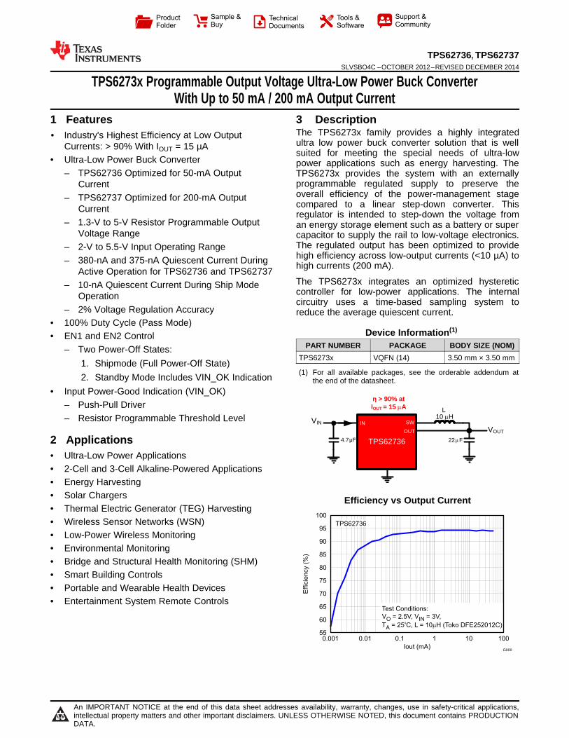
> 90% at IOUT = 15 PA
IN SW
OUT
Product
Folder
Sample &Buy
Technical
Documents
Tools &
Software
Support &Community
TPS62736, TPS62737SLVSBO4C –OCTOBER 2012–REVISED DECEMBER 2014
TPS6273x Programmable Output Voltage Ultra-Low Power Buck ConverterWith Up to 50 mA / 200 mA Output Current
1 Features 3 DescriptionThe TPS6273x family provides a highly integrated
1• Industry's Highest Efficiency at Low Outputultra low power buck converter solution that is wellCurrents: > 90% With IOUT = 15 µAsuited for meeting the special needs of ultra-low
• Ultra-Low Power Buck Converter power applications such as energy harvesting. The– TPS62736 Optimized for 50-mA Output TPS6273x provides the system with an externally
programmable regulated supply to preserve theCurrentoverall efficiency of the power-management stage– TPS62737 Optimized for 200-mA Outputcompared to a linear step-down converter. ThisCurrent regulator is intended to step-down the voltage from
– 1.3-V to 5-V Resistor Programmable Output an energy storage element such as a battery or superVoltage Range capacitor to supply the rail to low-voltage electronics.
The regulated output has been optimized to provide– 2-V to 5.5-V Input Operating Rangehigh efficiency across low-output currents (<10 µA) to– 380-nA and 375-nA Quiescent Current During high currents (200 mA).Active Operation for TPS62736 and TPS62737The TPS6273x integrates an optimized hysteretic– 10-nA Quiescent Current During Ship Modecontroller for low-power applications. The internalOperation circuitry uses a time-based sampling system to
– 2% Voltage Regulation Accuracy reduce the average quiescent current.• 100% Duty Cycle (Pass Mode)
Device Information(1)• EN1 and EN2 Control
PART NUMBER PACKAGE BODY SIZE (NOM)– Two Power-Off States:TPS6273x VQFN (14) 3.50 mm × 3.50 mm1. Shipmode (Full Power-Off State)(1) For all available packages, see the orderable addendum at2. Standby Mode Includes VIN_OK Indication the end of the datasheet.
• Input Power-Good Indication (VIN_OK)– Push-Pull Driver– Resistor Programmable Threshold Level
2 Applications• Ultra-Low Power Applications• 2-Cell and 3-Cell Alkaline-Powered Applications• Energy Harvesting• Solar Chargers Efficiency vs Output Current• Thermal Electric Generator (TEG) Harvesting• Wireless Sensor Networks (WSN)• Low-Power Wireless Monitoring• Environmental Monitoring• Bridge and Structural Health Monitoring (SHM)• Smart Building Controls• Portable and Wearable Health Devices• Entertainment System Remote Controls
1
An IMPORTANT NOTICE at the end of this data sheet addresses availability, warranty, changes, use in safety-critical applications,intellectual property matters and other important disclaimers. UNLESS OTHERWISE NOTED, this document contains PRODUCTIONDATA.
TPS62736, TPS62737SLVSBO4C –OCTOBER 2012–REVISED DECEMBER 2014 www.ti.com
Table of Contents9.3 Feature Description................................................. 181 Features .................................................................. 19.4 Device Functional Modes........................................ 202 Applications ........................................................... 1
10 Application and Implementation........................ 213 Description ............................................................. 110.1 Application Information.......................................... 214 Revision History..................................................... 210.2 Typical Applications ............................................. 215 Description (continued)......................................... 3
11 Power Supply Recommendations ..................... 286 Device Voltage Options......................................... 312 Layout................................................................... 287 Pin Configuration and Functions ......................... 4
12.1 Layout Guidelines ................................................. 288 Specifications......................................................... 512.2 Layout Example .................................................... 288.1 Absolute Maximum Ratings ...................................... 5
13 Device and Documentation Support ................. 298.2 Handling Ratings ...................................................... 513.1 Device Support...................................................... 298.3 Recommended Operating Conditions....................... 513.2 Related Links ........................................................ 298.4 Thermal Information .................................................. 513.3 Trademarks ........................................................... 298.5 Electrical Characteristics........................................... 613.4 Electrostatic Discharge Caution............................ 298.6 Typical Characteristics .............................................. 813.5 Glossary ................................................................ 299 Detailed Description ............................................ 18
14 Mechanical, Packaging, and Orderable9.1 Overview ................................................................. 18 Information ........................................................... 299.2 Functional Block Diagram ....................................... 18
4 Revision History
Changes from Revision B (July 2013) to Revision C Page
• Added ESD Ratings table, Feature Description section, Device Functional Modes, Application and Implementationsection, Power Supply Recommendations section, Layout section, Device and Documentation Support section, andMechanical, Packaging, and Orderable Information section. ................................................................................................ 1
Changes from Revision A (March 2013) to Revision B Page
• Added the TPS62737 Pinout information ............................................................................................................................... 4• Added graphs for TPS62737 to the Typical Characteristics................................................................................................. 13• Added the TPS62737 Application Circuit. ............................................................................................................................ 21• Changed Figure 72 .............................................................................................................................................................. 28• Added Figure 73 ................................................................................................................................................................... 28
Changes from Original (October 2012) to Revision A Page
• Changed the device From: Preview To: Active ...................................................................................................................... 1
2 Submit Documentation Feedback Copyright © 2012–2014, Texas Instruments Incorporated
Product Folder Links: TPS62736 TPS62737
TPS62736, TPS62737www.ti.com SLVSBO4C –OCTOBER 2012–REVISED DECEMBER 2014
5 Description (continued)To further assist users in the strict management of their energy budgets, the TPS6273x toggles the input power-good indicator to signal an attached microprocessor when the voltage on the input supply has dropped below apreset critical level. This signal is intended to trigger the reduction of load currents to prevent the system fromentering an undervoltage condition. In addition, independent enable signals allow the system to control whetherthe converter is regulating the output, monitoring only the input voltage, or to shut down in an ultra-low quiescentsleep state.
The input power-good threshold and output regulator levels are programmed independently through externalresistors.
All the capabilities of TPS6273x are packed into a small footprint 14-lead 3.5-mm × 3.5-mm QFN package(RGY).
6 Device Voltage Options
PART NO. OUTPUT VOLTAGE MAX OUTPUT CURRENT INPUT UVLOTPS62736 (1) Resistor Programmable 50 mA 2 VTPS62737 (1) Resistor Programmable 200 mA 2 V
(1) The RGY package is available in tape on reel. Add R suffix to order quantities of 3000 parts per reel, T suffix for 250 parts per reel.
Copyright © 2012–2014, Texas Instruments Incorporated Submit Documentation Feedback 3
Product Folder Links: TPS62736 TPS62737
VOUT_SET
EN1
VIN
_OK
_SE
T
2
3
4
5
6
13
12
11
10
9
7 8
1 14
OUT
SW
NC
VIN_OK
VSS
INV
RD
IV
NC
SW
VSS
EN2VOUT_SET
EN1
VIN
_OK
_SE
T
2
3
4
5
6
13
12
11
10
9
7 8
1 14
OUT
SW
NC
EN2
VIN_OK
VSS
INV
RD
IV
NC
NC
NC
TPS62736, TPS62737SLVSBO4C –OCTOBER 2012–REVISED DECEMBER 2014 www.ti.com
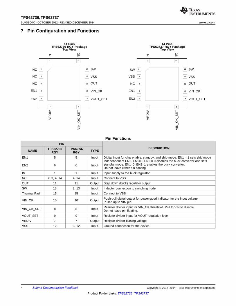
7 Pin Configuration and Functions
14 Pins 14 PinsTPS62736 RGY Package TPS62737 RGY Package
Top View Top View
Pin FunctionsPIN
DESCRIPTIONTPS62736 TPS62737NAME TYPERGY RGYEN1 5 5 Input Digital input for chip enable, standby, and ship-mode. EN1 = 1 sets ship mode
independent of EN2. EN1=0, EN2 = 0 disables the buck converter and setsstandby mode. EN1=0, EN2=1 enables the buck converter.EN2 6 6 InputDo not leave either pin floating.
IN 1 1 Input Input supply to the buck regulatorNC 2, 3, 4, 14 4, 14 Input Connect to VSSOUT 11 11 Output Step down (buck) regulator outputSW 13 2, 13 Input Inductor connection to switching nodeThermal Pad 15 15 Input Connect to VSS
Push-pull digital output for power-good indicator for the input voltage.VIN_OK 10 10 Output Pulled up to VIN pin.Resistor divider input for VIN_OK threshold. Pull to VIN to disable.VIN_OK_SET 8 8 Input Do not leave pin floating.
VOUT_SET 9 9 Input Resistor divider input for VOUT regulation levelVRDIV 7 7 Output Resistor divider biasing voltageVSS 12 3, 12 Input Ground connection for the device
4 Submit Documentation Feedback Copyright © 2012–2014, Texas Instruments Incorporated
Product Folder Links: TPS62736 TPS62737
TPS62736, TPS62737www.ti.com SLVSBO4C –OCTOBER 2012–REVISED DECEMBER 2014
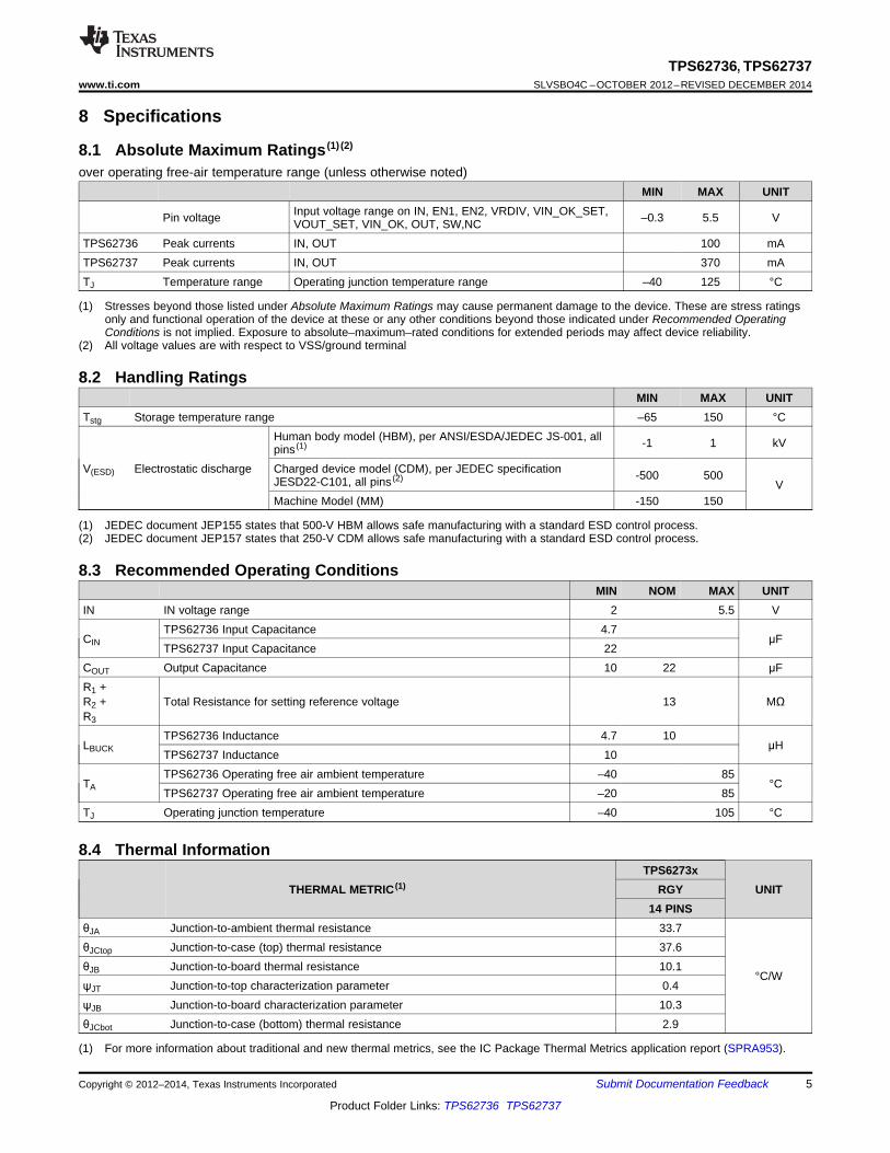
8 Specifications
8.1 Absolute Maximum Ratings (1) (2)
over operating free-air temperature range (unless otherwise noted)MIN MAX UNIT
Input voltage range on IN, EN1, EN2, VRDIV, VIN_OK_SET,Pin voltage –0.3 5.5 VVOUT_SET, VIN_OK, OUT, SW,NCTPS62736 Peak currents IN, OUT 100 mATPS62737 Peak currents IN, OUT 370 mATJ Temperature range Operating junction temperature range –40 125 °C
(1) Stresses beyond those listed under Absolute Maximum Ratings may cause permanent damage to the device. These are stress ratingsonly and functional operation of the device at these or any other conditions beyond those indicated under Recommended OperatingConditions is not implied. Exposure to absolute–maximum–rated conditions for extended periods may affect device reliability.
(2) All voltage values are with respect to VSS/ground terminal
8.2 Handling RatingsMIN MAX UNIT
Tstg Storage temperature range –65 150 °CHuman body model (HBM), per ANSI/ESDA/JEDEC JS-001, all -1 1 kVpins (1)
V(ESD) Electrostatic discharge Charged device model (CDM), per JEDEC specification -500 500JESD22-C101, all pins (2) VMachine Model (MM) -150 150
(1) JEDEC document JEP155 states that 500-V HBM allows safe manufacturing with a standard ESD control process.(2) JEDEC document JEP157 states that 250-V CDM allows safe manufacturing with a standard ESD control process.
8.3 Recommended Operating ConditionsMIN NOM MAX UNIT
IN IN voltage range 2 5.5 VTPS62736 Input Capacitance 4.7
CIN μFTPS62737 Input Capacitance 22
COUT Output Capacitance 10 22 μFR1 +R2 + Total Resistance for setting reference voltage 13 MΩR3
TPS62736 Inductance 4.7 10LBUCK μH
TPS62737 Inductance 10TPS62736 Operating free air ambient temperature –40 85
TA °CTPS62737 Operating free air ambient temperature –20 85
TJ Operating junction temperature –40 105 °C
8.4 Thermal InformationTPS6273x
THERMAL METRIC (1) RGY UNIT14 PINS
θJA Junction-to-ambient thermal resistance 33.7θJCtop Junction-to-case (top) thermal resistance 37.6θJB Junction-to-board thermal resistance 10.1
°C/WψJT Junction-to-top characterization parameter 0.4ψJB Junction-to-board characterization parameter 10.3θJCbot Junction-to-case (bottom) thermal resistance 2.9
(1) For more information about traditional and new thermal metrics, see the IC Package Thermal Metrics application report (SPRA953).
Copyright © 2012–2014, Texas Instruments Incorporated Submit Documentation Feedback 5
Product Folder Links: TPS62736 TPS62737
TPS62736, TPS62737SLVSBO4C –OCTOBER 2012–REVISED DECEMBER 2014 www.ti.com
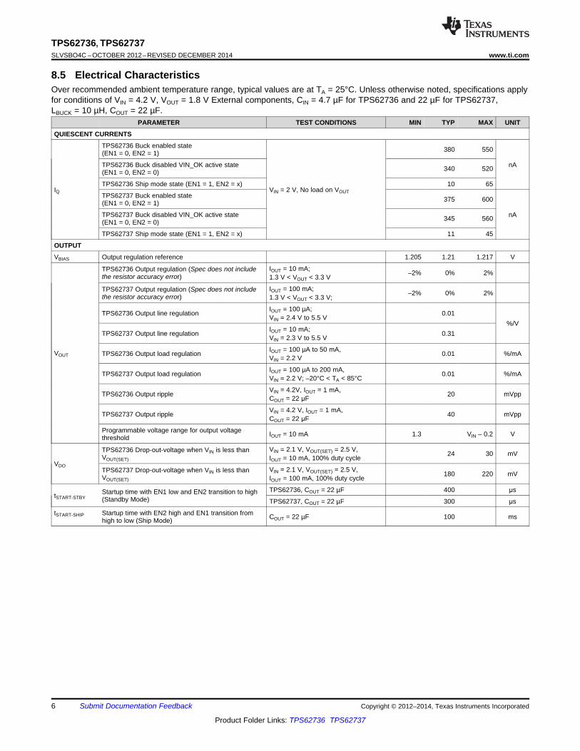
8.5 Electrical CharacteristicsOver recommended ambient temperature range, typical values are at TA = 25°C. Unless otherwise noted, specifications applyfor conditions of VIN = 4.2 V, VOUT = 1.8 V External components, CIN = 4.7 µF for TPS62736 and 22 µF for TPS62737,LBUCK = 10 µH, COUT = 22 µF.
PARAMETER TEST CONDITIONS MIN TYP MAX UNIT
QUIESCENT CURRENTS
TPS62736 Buck enabled state 380 550(EN1 = 0, EN2 = 1)
TPS62736 Buck disabled VIN_OK active state nA340 520(EN1 = 0, EN2 = 0)
TPS62736 Ship mode state (EN1 = 1, EN2 = x) 10 65IQ VIN = 2 V, No load on VOUT
TPS62737 Buck enabled state 375 600(EN1 = 0, EN2 = 1)
TPS62737 Buck disabled VIN_OK active state nA345 560(EN1 = 0, EN2 = 0)
TPS62737 Ship mode state (EN1 = 1, EN2 = x) 11 45
OUTPUT
VBIAS Output regulation reference 1.205 1.21 1.217 V
IOUT = 10 mA;TPS62736 Output regulation (Spec does not include –2% 0% 2%the resistor accuracy error) 1.3 V < VOUT < 3.3 V
IOUT = 100 mA;TPS62737 Output regulation (Spec does not include –2% 0% 2%the resistor accuracy error) 1.3 V < VOUT < 3.3 V;
IOUT = 100 µA;TPS62736 Output line regulation 0.01VIN = 2.4 V to 5.5 V%/V
IOUT = 10 mA;TPS62737 Output line regulation 0.31VIN = 2.3 V to 5.5 V
IOUT = 100 µA to 50 mA,VOUT TPS62736 Output load regulation 0.01 %/mAVIN = 2.2 V
IOUT = 100 µA to 200 mA,TPS62737 Output load regulation 0.01 %/mAVIN = 2.2 V; –20°C < TA < 85°C
VIN = 4.2V, IOUT = 1 mA,TPS62736 Output ripple 20 mVppCOUT = 22 μF
VIN = 4.2 V, IOUT = 1 mA,TPS62737 Output ripple 40 mVppCOUT = 22 μF
Programmable voltage range for output voltage IOUT = 10 mA 1.3 VIN – 0.2 Vthreshold
VIN = 2.1 V, VOUT(SET) = 2.5 V,TPS62736 Drop-out-voltage when VIN is less than 24 30 mVVOUT(SET) IOUT = 10 mA, 100% duty cycleVDO
VIN = 2.1 V, VOUT(SET) = 2.5 V,TPS62737 Drop-out-voltage when VIN is less than 180 220 mVVOUT(SET) IOUT = 100 mA, 100% duty cycle
TPS62736, COUT = 22 µF 400 μsStartup time with EN1 low and EN2 transition to hightSTART-STBY (Standby Mode) TPS62737, COUT = 22 µF 300 μs
tSTART-SHIP Startup time with EN2 high and EN1 transition from COUT = 22 µF 100 mshigh to low (Ship Mode)
6 Submit Documentation Feedback Copyright © 2012–2014, Texas Instruments Incorporated
Product Folder Links: TPS62736 TPS62737
TPS62736, TPS62737www.ti.com SLVSBO4C –OCTOBER 2012–REVISED DECEMBER 2014
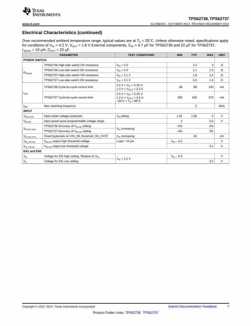
Electrical Characteristics (continued)Over recommended ambient temperature range, typical values are at TA = 25°C. Unless otherwise noted, specifications applyfor conditions of VIN = 4.2 V, VOUT = 1.8 V External components, CIN = 4.7 µF for TPS62736 and 22 µF for TPS62737,LBUCK = 10 µH, COUT = 22 µF.
PARAMETER TEST CONDITIONS MIN TYP MAX UNIT
POWER SWITCH
TPS62736 High-side switch ON resistance VIN = 3 V 2.4 3 Ω
TPS62736 Low-side switch ON resistance VIN = 3 V 1.1 1.5 ΩRDS(on)
TPS62737 High-side switch ON resistance VIN = 2.1 V 1.8 2.2 Ω
TPS62737 Low-side switch ON resistance VIN = 2.1 V 0.9 1.3 Ω
2.4 V < VIN < 5.25 V;TPS62736 Cycle-by-cycle current limit 68 86 100 mA1.3 V < VOUT < 3.3 VILIM 2.4 V < VIN < 5.25 V;
TPS62737 Cycle-by-cycle current limit 295 340 370 mA1.3 V < VOUT < 3.3 V;–20°C < TA < 85°C
fSW Max switching frequency 2 MHz
INPUT
VIN-UVLO Input under voltage protection VIN falling 1.91 1.95 2 V
VIN-OK Input power-good programmable voltage range 2 5.5 V
TPS62736 Accuracy of VIN-OK setting –2% 2%VIN-OK-ACC VIN increasing
TPS62737 Accuracy of VIN-OK setting –3% 3%
VIN-OK-HYS Fixed hysteresis on VIN_OK threshold, OK_HYST VIN increasing 40 mV
VIN_OK-OH VIN-OK output high threshold voltage Load = 10 µA VIN – 0.2 V
VIN_OK-OL VIN-OK output low threshold voltage 0.1 V
EN1 and EN2
VIH Voltage for EN High setting. Relative to VIN VIN – 0.2 VVIN = 4.2 V
VIL Voltage for EN Low setting 0.2 V
Copyright © 2012–2014, Texas Instruments Incorporated Submit Documentation Feedback 7
Product Folder Links: TPS62736 TPS62737
50
55
60
65
70
75
80
85
90
95
100
0.001 0.01 0.1 1 10 100
Effi
cien
cy (
%)
IOUT (mA)
Series2
Series4
Series5
Series6
C001
Test Conditions: VO = 2.5 V, TA = 25C L = 10 µH (Toko DFE252012C)
VIN = 4.2 V VIN = 3.6 V VIN = 3 V VIN = 2.7 V
88
90
92
94
96
98
100
2.0 2.5 3.0 3.5 4.0 4.5 5.0 5.5
Effi
cien
cy (
%)
VIN (V)
Series1 Series2 Series4 Series5
C002
IO = 0.1 mA IO = 1 mA IO = 10 mA IO = 45 mA
Test Conditions: VO = 2.5 V, TA = 25C L = 10 µH (Toko DFE252012C
TPS62736, TPS62737SLVSBO4C –OCTOBER 2012–REVISED DECEMBER 2014 www.ti.com
8.6 Typical CharacteristicsTable 1. Table of Graphs for TPS62736
Unless otherwise noted, graphs were taken using Figure 62 with L = Toko 10 µH DFE252012C FIGUREvs Output Current Figure 1
VO = 2.5 V Efficiencyvs Input Voltage Figure 2vs Output Current Figure 3
η VO = 1.8 V Efficiencyvs Input Voltage Figure 4vs Output Current Figure 5
VO = 1.3 V Efficiencyvs Input Voltage Figure 6vs Output Current Figure 7
VO = 2.5 V vs Input Voltage Figure 8vs Temperature Figure 9vs Output Current Figure 10
VOUT (DC) VO = 1.8 V vs Input Voltage Figure 11vs Temperature Figure 12vs Output Current Figure 13
VO = 1.3 V vs Input Voltage Figure 14vs Temperature Figure 15
VO = 2.5 V Figure 16IOUT MAX (DC) VO = 1.8 V vs Input Voltage Figure 17
VO = 1.3 V Figure 18EN1 = 1, EN2 = 0 (Ship Mode) Figure 19
Input IQ EN1 = 0, EN2 = 0 (Standby Mode) vs Input Voltage Figure 20EN1 = 0, EN2 = 1 (Active Mode) Figure 21
vs Output Current Figure 23Switching Frequency VO = 2.5 V
vs Input Voltage Figure 24vs Output Current Figure 25
Output Ripple VO = 2.5 Vvs Input Voltage Figure 26
IN = Sourcemeter configured as voltage source and measuring IN = Sourcemeter configured as voltage source and measuringcurrent currentOUT = sourcemeter configured as current source to sink current OUT = sourcemeter configured as current source to sink currentand VCOMP > VOUT and VCOMP > VOUT
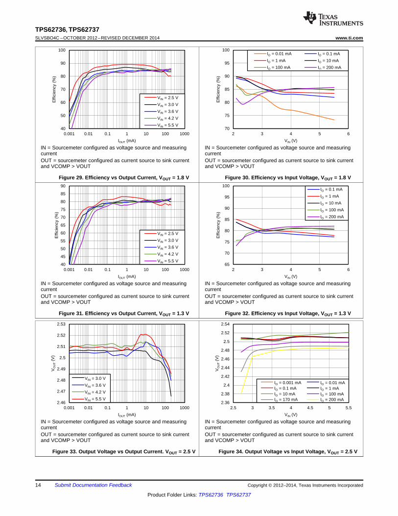
Figure 1. Efficiency vs Output Current, VOUT = 2.5 V Figure 2. Efficiency vs Input Voltage, VOUT = 2.5 V
8 Submit Documentation Feedback Copyright © 2012–2014, Texas Instruments Incorporated
Product Folder Links: TPS62736 TPS62737
2.495
2.500
2.505
2.510
2.515
2.520
0.001 0.01 0.1 1 10 100
VO
UT (
V)
IOUT (mA)
Series2 Series1 Series4 Series5
C007
VIN = 4.2 V VIN = 3.6 V VIN = 3 V VIN = 2.7 V
Test Conditions: VO = 2.5 V, TA = 25C L = 10 µH (Toko DFE252012C)
1.8
1.9
2.0
2.1
2.2
2.3
2.4
2.5
2.6
2.0 2.5 3.0 3.5 4.0 4.5 5.0 5.5
VO
UT (
V)
VIN (V)
Series1
Series2
Series4
Series5
C008
IO = 0.1 mA
IO = 1 mA
IO = 10 mA
IO = 45 mA
Test Conditions: VO = 2.5 V, TA = 25C L = 10 µH (Toko DFE252012C)
30 35 40 45 50 55 60 65 70 75 80 85 90 95
100
0.001 0.01 0.1 1 10 100
Effi
cien
cy (
%)
IOUT (mA)
Series1 Series2 Series4 Series5
C00
VIN = 4.2 V VIN = 3.6 V VIN = 3 V VIN = 2.1 V
Test Conditions: VO = 1.3 V, TA = 25C L = 10 µH (Toko DFE252012C)
80
82
84
86
88
90
92
94
96
98
100
2.0 2.5 3.0 3.5 4.0 4.5 5.0 5.5
Effi
cien
cy (
%)
VIN (V)
Series1 Series2 Series4 Series5
C006
IO = 45 mA
IO = 1 mA IO = 10 mA
IO = 0.1 mA Test Conditions: VO = 1.3 V, TA = 25C L = 10 µH (Toko DFE252012C)
40
45
50
55
60
65
70
75
80
85
90
95
100
0.001 0.01 0.1 1 10 100
Effi
cien
cy (
%)
IOUT (mA)
Series1
Series2
Series4
Series5
C003
VIN = 4.2 V
VIN = 2.1 V
VIN = 3 V
VIN = 3.6 V Test Conditions: VO = 1.8 V, TA = 25C L = 10 µH (Toko DFE252012C)
84
86
88
90
92
94
96
98
100
2.0 2.5 3.0 3.5 4.0 4.5 5.0 5.5
Effi
cien
cy
(%)
VIN (V)
Series1
Series2
Series4
Series5
C004
IO = 0.1 mA
IO = 1 mA
IO = 10 mA
IO = 45 mA
Test Conditions: VO = 1.8 V, TA = 25C L = 10 µH (Toko DFE252012C)
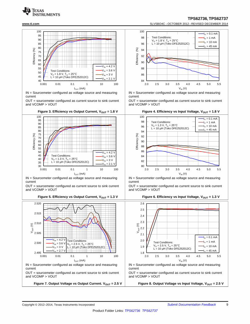
TPS62736, TPS62737www.ti.com SLVSBO4C –OCTOBER 2012–REVISED DECEMBER 2014
IN = Sourcemeter configured as voltage source and measuring IN = Sourcemeter configured as voltage source and measuringcurrent currentOUT = sourcemeter configured as current source to sink current OUT = sourcemeter configured as current source to sink currentand VCOMP > VOUT and VCOMP > VOUT
Figure 3. Efficiency vs Output Current, VOUT = 1.8 V Figure 4. Efficiency vs Input Voltage, VOUT = 1.8 V
IN = Sourcemeter configured as voltage source and measuring IN = Sourcemeter configured as voltage source and measuringcurrent currentOUT = sourcemeter configured as current source to sink current OUT = sourcemeter configured as current source to sink currentand VCOMP > VOUT and VCOMP > VOUT
Figure 5. Efficiency vs Output Current, VOUT = 1.3 V Figure 6. Efficiency vs Input Voltage, VOUT = 1.3 V
IN = Sourcemeter configured as voltage source and measuring IN = Sourcemeter configured as voltage source and measuringcurrent currentOUT = sourcemeter configured as current source to sink current OUT = sourcemeter configured as current source to sink currentand VCOMP > VOUT and VCOMP > VOUT
Figure 7. Output Voltage vs Output Current. VOUT = 2.5 V Figure 8. Output Voltage vs Input Voltage, VOUT = 2.5 V
Copyright © 2012–2014, Texas Instruments Incorporated Submit Documentation Feedback 9
Product Folder Links: TPS62736 TPS62737
1.289
1.291
1.293
1.295
1.297
1.299
1.301
1.303
0.001 0.01 0.1 1 10 100
VO
UT (
V)
IOUT (mA)
Series1 Series2 Series4 Series5
C013
VIN = 4.2 V
VIN = 3.6 V VIN = 3 V
VIN = 2.1 V
Test Conditions: VO = 1.3 V, TA = 25C L = 10 uH (Toko DFE252012C)
1.28
1.285
1.29
1.295
1.3
1.305
2.0 2.5 3.0 3.5 4.0 4.5 5.0 5.5
VO
UT (
V)
VIN (V)
Series1 Series2 Series4 Series5
C014
IO = 10 mA IO = 45 mA
IO = 1 mA IO = 0.1 mA Test Condition:
VO = 1.3 V, TA = 25C L = 10 µH (Toko DFE252012C)
1.78
1.785
1.79
1.795
1.8
1.805
1.81
1.815
2.0 2.5 3.0 3.5 4.0 4.5 5.0 5.5
VO
UT
(V)
VIN (V)
Series1 Series2 Series4 Series5
C011
IO = 0.1 mA IO = 1 mA IO = 10 mA IO = 45 mA
Test Conditions: VO = 1.8 V, TA = 25C L = 10 µH (Toko DFE252012C)
1.78
1.785
1.79
1.795
1.8
1.805
±40 ±20 0 20 40 60 80
VO
UT (
V)
Temperature (C)
Series1
Series2
Series4
C012
IO = 1 mA IO = 10 mA IO = 50 mA
Test Conditions: VO = 1.8 V, VIN = 3 V L = 10 µH (Toko DFE252012C)
2.485
2.490
2.495
2.500
2.505
2.510
2.515
2.520
2.525
±40 ±20 0 20 40 60 80
VO
UT (
V)
Temperature (C)
Series1
Series2
Series4
C009
IO = 1 mA
IO = 10 mA
IO = 50 mA
Test Conditions: VO = 2.5 V, VIN = 3 V L = 10 µH (Toko DFE252012C)
1.780
1.785
1.790
1.795
1.800
1.805
0.001 0.01 0.1 1 10 100
VO
UT (
V)
IOUT (mA)
Series1 Series2 Series4 Series5
C010
VIN = 4.2 V VIN = 3.6 V
VIN = 2.7 V VIN = 3 V
Test Conditions: VO = 1.8 V, TA = 25C L = 10 µH (Toko DFE252012C)
TPS62736, TPS62737SLVSBO4C –OCTOBER 2012–REVISED DECEMBER 2014 www.ti.com
IN = Sourcemeter configured as voltage source and measuring IN = Sourcemeter configured as voltage source and measuringcurrent currentOUT = sourcemeter configured as current source to sink current OUT = sourcemeter configured as current source to sink currentand VCOMP > VOUT and VCOMP > VOUTThermal stream provided temperature variation
Figure 9. Output Voltage vs Temperature, VOUT = 2.5 V Figure 10. Output Voltage vs Output Current, VOUT = 1.8 V
IN = Sourcemeter configured as voltage source and measuring IN = Sourcemeter configured as voltage source and measuringcurrent currentOUT = sourcemeter configured as current source to sink current OUT = sourcemeter configured as current source to sink currentand VCOMP > VOUT and VCOMP > VOUT
Thermal stream provided temperature variation
Figure 11. Output Voltage vs Input Voltage, VOUT = 1.8 V Figure 12. Output Voltage vs Temperature, VOUT = 1.8 V
IN = Sourcemeter configured as voltage source and measuring IN = Sourcemeter configured as voltage source and measuringcurrent currentOUT = sourcemeter configured as current source to sink current OUT = sourcemeter configured as current source to sink currentand VCOMP > VOUT and VCOMP > VOUT
Figure 13. Output Voltage vs Output Current, VOUT = 1.3 V Figure 14. Output Voltage vs Input Voltage, VOUT = 1.3 V
10 Submit Documentation Feedback Copyright © 2012–2014, Texas Instruments Incorporated
Product Folder Links: TPS62736 TPS62737
0
50
100
150
200
250
300
350
400
450
2.0 2.5 3.0 3.5 4.0 4.5 5.0 5.5
Inpu
t Q
uies
cent
Cur
rent
(nA
)
Input Voltage (V)
T = 85C
T = 55C
T = 25C
T = 0C
TA = -40 C
TA = 85°C TA = 55°C
TA = 25°C
TA = 0°C TA = ±40°C
C019
0
200
400
600
800
1000
1200
2.0 2.5 3.0 3.5 4.0 4.5 5.0 5.5
Inpu
t Q
uies
cent
Cur
rent
(nA
)
Input Voltage (V)
T=85C
T=55C
T=25C
T=0C
TA = -40 C
TA = 85°C TA = 55°C
TA = 25°C TA = 0°C TA = ±40°C
C020
40
50
60
70
80
90
100
2.0 2.5 3.0 3.5 4.0 4.5 5.0 5.5
Max
imum
Out
put
Cur
rent
(m
A)
VIN (V)
Series1
Series2
Series4
Series5
C017
TA = ±40C TA = 0C TA = 25C TA = 85C
Test Conditions: VO =1.8 V ± 100 mV L = 10 µH (Toko DFE252012C)
40
50
60
70
80
90
100
2.0 2.5 3.0 3.5 4.0 4.5 5.0 5.5
Max
imum
Out
put
Cur
rent
(m
A)
VIN (V)
Series1
Series2
Series4
Series5
C018
TA = 0C TA = 25C
TA = ±40C
TA = 85C
Test Conditions: VO = 1.3 V ± 100 mV L = 10 µH (Toko DFE252012C)
1.285
1.290
1.295
1.300
1.305
-40 -20 0 20 40 60 80
VO
UT
(V
)
Temperature (C)
Series1
Series2
Series4
C015
IO = 1 mA
IO = 10 mA IO = 50 mA
Test Conditions: VO =1.3 V, VIN = 3 V L = 10 µH (Toko DFE252012C)
0
20
40
60
80
100
2.0 2.5 3.0 3.5 4.0 4.5 5.0 5.5
Max
imum
Out
put
Cur
rent
(m
A)
VIN (V)
Series1
Series2
Series4
Series5
C016
TA = ±40C
TA = 25C TA = 0C
TA = 85C
Test Conditions: VO = 2.5 V ± 100 mV L = 10 µH (Toko DFE252012C)
TPS62736, TPS62737www.ti.com SLVSBO4C –OCTOBER 2012–REVISED DECEMBER 2014
IN = Sourcemeter configured as voltage source and measuring IN = Sourcemeter configured as voltage source and measuringcurrent currentVOUT = sourcemeter configured as current source to sink current OUT = sourcemeter configured as current source to increasinglyand VCOMP > VOUT sink current until V(OUT) < VOUT - 100 mVThermal stream provided temperature variation Thermal stream provided temperature variation
Figure 15. Output Voltage vs Temperature, VOUT = 1.3 V Figure 16. Maximum Output Current vs Input Voltage,VOUT = 2.5 V
IN = Sourcemeter configured as voltage source and measuringIN = Sourcemeter configured as voltage source and measuringcurrentcurrentOUT = sourcemeter configured as current source to increasinglyOUT = sourcemeter configured as current source to increasinglysink current until V(OUT) < VOUT - 100 mVsink current until V(OUT) < VOUT - 100 mVThermal stream provided temperature variationThermal stream provided temperature variation
Figure 18. Maximum Output Current vs Input Voltage,Figure 17. Maximum Output Current vs Input Voltage,VOUT = 1.3 VVOUT = 1.8 V
IN = Sourcemeter configured as voltage source and measuring IN = Sourcemeter configured as voltage source and measuringcurrent currentOUT = open; EN1 = high; EN2 = x OUT = open; EN1 = EN2 = lowThermal stream provided temperature variation Thermal stream provided temperature variation
Figure 19. Input Quiescent Current Figure 20. Input Quiescent Currentvs Input Voltage Ship Mode vs Input Voltage Standby Mode
Copyright © 2012–2014, Texas Instruments Incorporated Submit Documentation Feedback 11
Product Folder Links: TPS62736 TPS62737
0
5
10
15
20
25
0 10 20 30 40 50 60
Out
put V
olta
ge R
ippl
e (m
VP
P)
Output Current (mA)
Vin = 2 V
Vin = 3 V
Vin = 4 V
Vin = 5 V
VIN = 2 V
C025
VIN = 3 V
VIN = 4 V
VIN = 5 V
VO = 1.3 V C = 22 PF
0
5
10
15
20
25
30
2.0 2.5 3.0 3.5 4.0 4.5 5.0 5.5
Out
put V
olta
ge R
ippl
e (m
VP
P)
Input Voltage (V)
Iout=100uA
I=1mA
I=10mA
I=50mA
IOUT = 100 A
C024
IOUT = 1 mA
IOUT = 10 mA
IOUT = 50 mA
VO = 1.3 V C = 22 PF
0
20
40
60
80
100
120
0 10 20 30 40 50 60
Maj
or S
witc
hing
Fre
quen
cy (
kHz)
Output Current (mA)
Vin = 2 V
Vin = 3 V
Vin = 4 V
Vin = 5 V
VIN = 2 V
C022
VIN = 3 V
VIN = 4 V
VIN = 5 V
VO = 1.3 V L = 10 PH
0 10 20 30 40 50 60 70 80 90
100 110 120 130
2.0 2.5 3.0 3.5 4.0 4.5 5.0 5.5
Maj
or S
witc
hing
Fre
quen
cy (
kHz)
Input Voltage (V)
Iout=100uA
I=1mA
I=10mA
I=50mA
IOUT = 100 A
C023
IOUT = 1 mA
IOUT = 10 mA
IOUT = 50 mA
VO = 1.3 V L = 10P+
0
200
400
600
800
1000
1200
2.0 2.5 3.0 3.5 4.0 4.5 5.0 5.5
Inpu
t Q
uies
cent
Cur
rent
(nA
)
Input Voltage (V)
T=85C T=55C T=25C T=0C T = -40 C
TA = 85°C TA = 55°C TA = 25°C TA = 0°C TA = ±40°C
C021
0
100
200
300
400
500
600
700
800
2.0 2.5 3.0 3.5 4.0 4.5 5.0 5.5
Inpu
t Q
uies
cent
Cur
rent
(nA
)
Input Voltage (V)
Rsum=1M
Rsum=13M
C026
Rsum = 1 M
Rsum = 13 M
TPS62736, TPS62737SLVSBO4C –OCTOBER 2012–REVISED DECEMBER 2014 www.ti.com
IN = Sourcemeter configured as voltage source and measuring IN = Sourcemeter configured as voltage source and measuringcurrent currentOUT = sourcemeter configured as voltage source > VOUT to OUT = sourcemeter configured as voltage source > VOUT toprevent switching prevent switchingThermal stream provided temperature variation Thermal stream provided temperature variation
Figure 21. Input Quiescent Current Figure 22. Input Quiescent Currentvs Input Voltage Active Mode vs Input Voltage Active Mode where RSUM = R1 + R2 + R3
IN = Sourcemeter configured as voltage source IN = Sourcemeter configured as voltage sourceOUT = sourcemeter configured as current source to sink current OUT = sourcemeter configured as current source to sink currentand VCOMP > VOUT and VCOMP > VOUT
Figure 23. Major Switching Frequency vs Output Current Figure 24. Major Switching Frequency vs Input Voltage
IN = Sourcemeter configured as voltage sourceIN = Sourcemeter configured as voltage sourceOUT = sourcemeter configured as current source to sink currentOUT = sourcemeter configured as current source to sink currentand VCOMP > VOUTand VCOMP > VOUTScope probe with small ground lead used to measure rippleScope probe with small ground lead used to measure rippleacross COUTacross COUT
Figure 26. Output Voltage Ripple vs Input VoltageFigure 25. Output Voltage Ripple vs Output Current
12 Submit Documentation Feedback Copyright © 2012–2014, Texas Instruments Incorporated
Product Folder Links: TPS62736 TPS62737
40
50
60
70
80
90
100
0.001 0.01 0.1 1 10 100 1000
Effi
cien
cy (
%)
IOUT (mA)
VIN = 5.5 V
VIN = 2.3 V
VIN = 2.5 V
C048
VIN = 3.0 V
VIN = 4.2 V
VIN = 5.5 V 75.0
80.0
85.0
90.0
95.0
100.0
2.5 3 3.5 4 4.5 5 5.5
Effi
cien
cy (
%)
VIN (V)
IO = 0.1 mAIO = 1 mAIO = 10 mAIO = 100 mAIO = 200 mA
C045
IO = 0.1 mA IO = 1 mA IO = 10 mA IO = 100 mA IO = 200 mA
TPS62736, TPS62737www.ti.com SLVSBO4C –OCTOBER 2012–REVISED DECEMBER 2014
Table 2. Table of Graphs for TPS62737Unless otherwise noted, graphs were taken using Figure 52 with L = Toko 10 µH DFE252012C FIGURE
vs Output Current Figure 27VO = 2.5 V Efficiency
vs Input Voltage Figure 28vs Output Current Figure 29
η VO = 1.8 V Efficiencyvs Input Voltage Figure 30vs Output Current Figure 31
VO = 1.3 V Efficiencyvs Input Voltage Figure 32vs Output Current Figure 33
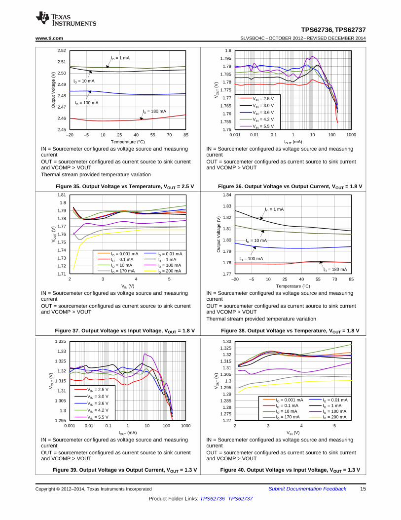
VO = 2.5 V vs Input Voltage Figure 33vs Temperature Figure 35vs Output Current Figure 36
VOUT (DC) VO = 1.8 V vs Input Voltage Figure 37vs Temperature Figure 38vs Output Current Figure 39
VO = 1.3 V vs Input Voltage Figure 40vs Temperature Figure 41
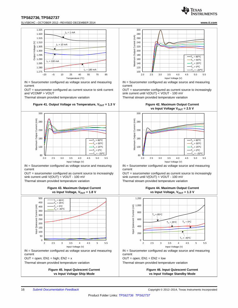
VO = 2.5 V Figure 42IOUT MAX (DC) VO = 1.8 V vs Input Voltage Figure 43
VO = 1.3 V Figure 44EN1 = 1, EN2 = 0 (Ship Mode) Figure 45
Input IQ EN1 = 0, EN2 = 0 (Standby Mode) vs Input Voltage Figure 46EN1 = 0, EN2 = 1 (Active Mode) Figure 47
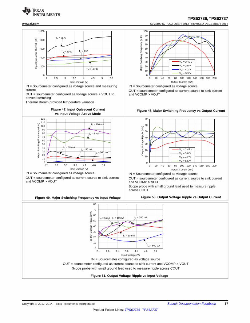
vs Output Current Figure 48Switching Frequency VO = 1.8 V
vs Input Voltage Figure 49vs Output Current Figure 51
Output Ripple VO = 1.8 Vvs Input Voltage Figure 51
IN = Sourcemeter configured as voltage source and measuring IN = Sourcemeter configured as voltage source and measuringcurrent currentOUT = sourcemeter configured as current source to sink current OUT = sourcemeter configured as current source to sink currentand VCOMP > VOUT and VCOMP > VOUT
Figure 27. Efficiency vs Output Current, VOUT = 2.5 V Figure 28. Efficiency vs Input Voltage, VOUT = 2.5 V
Copyright © 2012–2014, Texas Instruments Incorporated Submit Documentation Feedback 13
Product Folder Links: TPS62736 TPS62737
2.46
2.47
2.48
2.49
2.5
2.51
2.52
2.53
0.001 0.01 0.1 1 10 100 1000
VO
UT (
V)
IOUT (mA)
VIN = 3.0 V
VIN = 3.6 V
VIN = 4.2 V
VIN = 5.5 V
C061
VIN = 3.0 V
VIN = 3.6 V
VIN = 4.2 V
VIN = 5.5 V 2.36
2.38
2.4
2.42
2.44
2.46
2.48
2.5
2.52
2.54
2.5 3 3.5 4 4.5 5 5.5
VO
UT (
V)
VIN (V)
IO = 0.001 IO = 0.01 mAIO = 0.1 mA IO = 1 mAIO = 10 mA IO = 100 mAIO = 170 mA IO = 200 mA
C058
IO = 0.001 mA IO = 0.1 mA IO = 10 mA IO = 170 mA
IO = 0.01 mA IO = 1 mA IO = 100 mA IO = 200 mA
40
45
50
55
60
65
70
75
80
85
90
0.001 0.01 0.1 1 10 100 1000
Effi
cien
cy (
%)
IOUT (mA)
VIN = 2.5 V
VIN = 3.0 V
VIN = 3.6 V
VIN = 4.2 V
VIN = 5.5 V
C046
VIN = 2.5 V
VIN = 3.0 V
VIN = 3.6 V
VIN = 4.2 V
VIN = 5.5 V 65
70
75
80
85
90
95
100
2 3 4 5 6
Effi
cien
cy (
%)
VIN (V)
IO = 0.01 mA
IO = 1 mA
IO = 10 mA
IO = 100 mA
IO = 200 mA
C043
IO = 0.1 mA
IO = 1 mA
IO = 10 mA
IO = 100 mA
IO = 200 mA
40
50
60
70
80
90
100
0.001 0.01 0.1 1 10 100 1000
Effi
cien
cy (
%)
IOUT (mA)
VIN = 2.5 V
VIN = 3.0 V
VIN = 3.6 V
VIN = 4.2 V
VIN = 5.5 V
C047
VIN = 2.5 V
VIN = 3.0 V
VIN = 3.6 V
VIN = 4.2 V
VIN = 5.5 V 70
75
80
85
90
95
100
2 3 4 5 6
Effi
cien
cy (
%)
VIN (V)
IO = 0.01 mA IO = 0.1 mA
IO = 1 mA IO = 10 mA
IO = 100 mA IO = 200 mA
C044
IO = 0.01 mA
IO = 1 mA
IO = 100 mA
IO = 0.1 mA
IO = 10 mA
IO = 200 mA
TPS62736, TPS62737SLVSBO4C –OCTOBER 2012–REVISED DECEMBER 2014 www.ti.com
IN = Sourcemeter configured as voltage source and measuring IN = Sourcemeter configured as voltage source and measuringcurrent currentOUT = sourcemeter configured as current source to sink current OUT = sourcemeter configured as current source to sink currentand VCOMP > VOUT and VCOMP > VOUT
Figure 29. Efficiency vs Output Current, VOUT = 1.8 V Figure 30. Efficiency vs Input Voltage, VOUT = 1.8 V
IN = Sourcemeter configured as voltage source and measuring IN = Sourcemeter configured as voltage source and measuringcurrent currentOUT = sourcemeter configured as current source to sink current OUT = sourcemeter configured as current source to sink currentand VCOMP > VOUT and VCOMP > VOUT
Figure 31. Efficiency vs Output Current, VOUT = 1.3 V Figure 32. Efficiency vs Input Voltage, VOUT = 1.3 V
IN = Sourcemeter configured as voltage source and measuring IN = Sourcemeter configured as voltage source and measuringcurrent currentOUT = sourcemeter configured as current source to sink current OUT = sourcemeter configured as current source to sink currentand VCOMP > VOUT and VCOMP > VOUT
Figure 33. Output Voltage vs Output Current. VOUT = 2.5 V Figure 34. Output Voltage vs Input Voltage, VOUT = 2.5 V
14 Submit Documentation Feedback Copyright © 2012–2014, Texas Instruments Incorporated
Product Folder Links: TPS62736 TPS62737
1.295
1.3
1.305
1.31
1.315
1.32
1.325
1.33
1.335
0.001 0.01 0.1 1 10 100 1000
VO
UT (
V)
IOUT (mA)
VIN = 2.5 V
VIN = 3.0 V
VIN = 3.6 V
VIN = 4.2 V
VIN = 5.5 V
C059
VIN = 2.5 V
VIN = 3.0 V
VIN = 3.6 V
VIN = 4.2 V
VIN = 5.5 V 1.27
1.275
1.28
1.285
1.29
1.295
1.3
1.305
1.31
1.315
1.32
1.325
1.33
2 3 4 5
VO
UT (
V)
VIN (V)
IO = 0.001 IO = 0.01 mAIO = 0.1 mA IO = 1 mAIO = 10 mA IO = 100 mAIO = 170 mA IO = 200 mA
C056
IO = 0.001 mA IO = 0.1 mA IO = 10 mA IO = 170 mA
IO = 0.01 mA IO = 1 mA IO = 100 mA IO = 200 mA
1.71
1.72
1.73
1.74
1.75
1.76
1.77
1.78
1.79
1.8
1.81
2 3 4 5
VO
UT (
V)
VIN (V)
IO = 0.001 IO = 0.01 mAIO = 0.1 mA IO = 1 mAIO = 10 mA IO = 100 mAIO = 170 mA IO = 200 mA
C057
IO = 0.001 mA IO = 0.1 mA IO = 10 mA IO = 170 mA
IO = 0.01 mA IO = 1 mA IO = 100 mA IO = 200 mA
1.77
1.78
1.79
1.80
1.81
1.82
1.83
1.84
±20 ±5 10 25 40 55 70 85
Out
put V
olta
ge (
V)
Temperature (oC) C020
IO = 1 mA
IO = 10 mA
IO = 100 mA
IO = 180 mA
2.45
2.46
2.47
2.48
2.49
2.50
2.51
2.52
±20 ±5 10 25 40 55 70 85
Out
put V
olta
ge (
V)
Temperature (oC) C020
IO = 1 mA
IO = 10 mA
IO = 100 mA
IO = 180 mA
1.75
1.755
1.76
1.765
1.77
1.775
1.78
1.785
1.79
1.795
1.8
0.001 0.01 0.1 1 10 100 1000
VO
UT (
V)
IOUT (mA)
VIN = 2.5 V
VIN = 3.0 V
VIN = 3.6 V
VIN = 4.2 V
VIN = 5.5 V
C060
VIN = 2.5 V
VIN = 3.0 V
VIN = 3.6 V
VIN = 4.2 V
VIN = 5.5 V
TPS62736, TPS62737www.ti.com SLVSBO4C –OCTOBER 2012–REVISED DECEMBER 2014
IN = Sourcemeter configured as voltage source and measuring IN = Sourcemeter configured as voltage source and measuringcurrent currentOUT = sourcemeter configured as current source to sink current OUT = sourcemeter configured as current source to sink currentand VCOMP > VOUT and VCOMP > VOUTThermal stream provided temperature variation
Figure 35. Output Voltage vs Temperature, VOUT = 2.5 V Figure 36. Output Voltage vs Output Current, VOUT = 1.8 V
IN = Sourcemeter configured as voltage source and measuring IN = Sourcemeter configured as voltage source and measuringcurrent currentOUT = sourcemeter configured as current source to sink current OUT = sourcemeter configured as current source to sink currentand VCOMP > VOUT and VCOMP > VOUT
Thermal stream provided temperature variation
Figure 37. Output Voltage vs Input Voltage, VOUT = 1.8 V Figure 38. Output Voltage vs Temperature, VOUT = 1.8 V
IN = Sourcemeter configured as voltage source and measuring IN = Sourcemeter configured as voltage source and measuringcurrent currentOUT = sourcemeter configured as current source to sink current OUT = sourcemeter configured as current source to sink currentand VCOMP > VOUT and VCOMP > VOUT
Figure 39. Output Voltage vs Output Current, VOUT = 1.3 V Figure 40. Output Voltage vs Input Voltage, VOUT = 1.3 V
Copyright © 2012–2014, Texas Instruments Incorporated Submit Documentation Feedback 15
Product Folder Links: TPS62736 TPS62737
0
50
100
150
200
250
300
350
400
450
500
2 2.5 3 3.5 4 4.5 5 5.5
Inpu
t Q
uies
cent
Cur
rent
(nA
)
Input Voltage (V)
TA = 85 C TA = 25 C TA = 0 C TA = -40 C
C054
TA = 85oC TA = 25oC TA = 0oC TA = -40oC
0
200
400
600
800
1,000
1,200
2 2.5 3 3.5 4 4.5 5 5.5
Inpu
t Q
uies
cent
Cur
rent
(nA
)
Input Voltage (V) C055
TA = -40oC
TA = 25oC
TA = 85oC
TA = 0oC
80
130
180
230
280
330
2.0 2.5 3.0 3.5 4.0 4.5 5.0 5.5
Max
imum
Out
put
Cur
rent
(m
A)
Input Voltage (V)
T=85C
TA = 55
TA=25
TA=0
TA=-20
TA = 85°C TA = 55°C
TA = 25°C
TA = 0°C TA = ±20°C
C020
80
130
180
230
280
330
2.0 2.5 3.0 3.5 4.0 4.5 5.0 5.5
Max
imum
Out
put
Cur
rent
(m
A)
Input Voltage (V)
TA=85
TA = 55
TA=25
TA=0
TA=-20
TA = 85°C TA = 55°C
TA = 25°C
TA = 0°C TA = ±20°C
C020
1.275
1.280
1.285
1.290
1.295
1.300
1.305
1.310
1.315
1.320
1.325
±20 ±5 10 25 40 55 70 85
Out
put V
olta
ge (
V)
Temperature (oC) C020
IO = 1 mA
IO = 10 mA
IO = 100 mA
IO = 180 mA 100
120
140
160
180
200
220
240
260
280
300
2.0 2.5 3.0 3.5 4.0 4.5 5.0 5.5
Max
imum
Out
put
Cur
rent
(m
A)
Input Voltage (V)
T=85C
TA = 55
TA=25
TA=0
TA=-20
TA = 85°C TA = 55°C
TA = 25°C
TA = 0°C TA = ±20°C
C020
TPS62736, TPS62737SLVSBO4C –OCTOBER 2012–REVISED DECEMBER 2014 www.ti.com
IN = Sourcemeter configured as voltage source and measuring IN = Sourcemeter configured as voltage source and measuringcurrent currentOUT = sourcemeter configured as current source to sink current OUT = sourcemeter configured as current source to increasinglyand VCOMP > VOUT sink current until V(OUT) < VOUT - 100 mVThermal stream provided temperature variation Thermal stream provided temperature variation
Figure 41. Output Voltage vs Temperature, VOUT = 1.3 V Figure 42. Maximum Output Currentvs Input Voltage VOUT = 2.5 V
IN = Sourcemeter configured as voltage source and measuring IN = Sourcemeter configured as voltage source and measuringcurrent currentOUT = sourcemeter configured as current source to increasingly OUT = sourcemeter configured as current source to increasinglysink current until V(OUT) < VOUT - 100 mV sink current until V(OUT) < VOUT - 100 mVThermal stream provided temperature variation Thermal stream provided temperature variation
Figure 43. Maximum Output Current Figure 44. Maximum Output Currentvs Input Voltage, VOUT = 1.8 V vs Input Voltage, VOUT = 1.3 V
IN = Sourcemeter configured as voltage source and measuring IN = Sourcemeter configured as voltage source and measuringcurrent currentOUT = open; EN1 = high; EN2 = x OUT = open; EN1 = EN2 = lowThermal stream provided temperature variation Thermal stream provided temperature variation
Figure 45. Input Quiescent Current Figure 46. Input Quiescent Currentvs Input Voltage Ship Mode vs Input Voltage Standby Mode
16 Submit Documentation Feedback Copyright © 2012–2014, Texas Instruments Incorporated
Product Folder Links: TPS62736 TPS62737
0
10
20
30
40
50
60
70
80
2.1 2.6 3.1 3.6 4.1 4.6 5.1
Out
put V
olta
ge R
ippl
e (m
V)
Input Voltage (V) C052
IO = 5 mA
IO = 50 mA
IO = 500 PA
IO = 100 mA IO = 10 mA
0
10
20
30
40
50
60
70
0 20 40 60 80 100 120 140 160 180 200
Out
put
Vol
tage
Rip
ple
(mV
)
Output Current (mA)
VIN = 2.5 V
VIN = 3.0 V
VIN = 3.6 V
VIN = 4.2 V
C050
VIN = 2.45 V
VIN = 3.0 V
VIN = 4.2 V
VIN = 5.5 V 0
10
20
30
40
50
60
70
80
90
100
110
120
2.1 2.6 3.1 3.6 4.1 4.6 5.1
Maj
or S
witc
hing
Fre
quen
cy (
kHz)
Input Voltage (V) C051
IO = 500 PA IO = 50 mA
IO = 10 mA
IO = 5 mA
IO = 100 mA
0
200
400
600
800
1,000
2 2.5 3 3.5 4 4.5 5 5.5
Inpu
t Q
uies
cent
Cur
rent
(nA
)
Input Voltage (V) C053
TA = 85oC
TA = 25oC TA = 0oC
TA = -40oC
0
10
20
30
40
50
60
70
80
90
100
0 20 40 60 80 100 120 140 160 180 200
Maj
or S
witc
hing
Fre
quen
cy (
kHz)
Output Current (mA)
VIN = 2.5 V
VIN = 3.0 V
VIN = 3.6 V
VIN = 4.2 V
C049
VIN = 2.45 V
VIN = 3.0 V
VIN = 4.2 V
VIN = 5.5 V
TPS62736, TPS62737www.ti.com SLVSBO4C –OCTOBER 2012–REVISED DECEMBER 2014
IN = Sourcemeter configured as voltage source and measuring IN = Sourcemeter configured as voltage sourcecurrent OUT = sourcemeter configured as current source to sink currentOUT = sourcemeter configured as voltage source > VOUT to and VCOMP > VOUTprevent switchingThermal stream provided temperature variation
Figure 47. Input Quiescent Current Figure 48. Major Switching Frequency vs Output Currentvs Input Voltage Active Mode
IN = Sourcemeter configured as voltage source IN = Sourcemeter configured as voltage sourceOUT = sourcemeter configured as current source to sink current OUT = sourcemeter configured as current source to sink currentand VCOMP > VOUT and VCOMP > VOUT
Scope probe with small ground lead used to measure rippleacross COUT
Figure 50. Output Voltage Ripple vs Output CurrentFigure 49. Major Switching Frequency vs Input Voltage
IN = Sourcemeter configured as voltage sourceOUT = sourcemeter configured as current source to sink current and VCOMP > VOUT
Scope probe with small ground lead used to measure ripple across COUT
Figure 51. Output Voltage Ripple vs Input Voltage
Copyright © 2012–2014, Texas Instruments Incorporated Submit Documentation Feedback 17
Product Folder Links: TPS62736 TPS62737
Nano-Power Management
and Reference Generation
VIN_OK_SET
VIN_OK
IN VSS
EN1 VRDIV
VIN_UV
OK
+
UV
+
Vref
Input Threshold Control
Vref
SW
EN2
Buck
Controller
OUT
VOUT_SET
TPS6273x Functional Block
Diagram
VIN > UV?
TPS62736, TPS62737SLVSBO4C –OCTOBER 2012–REVISED DECEMBER 2014 www.ti.com
9 Detailed Description
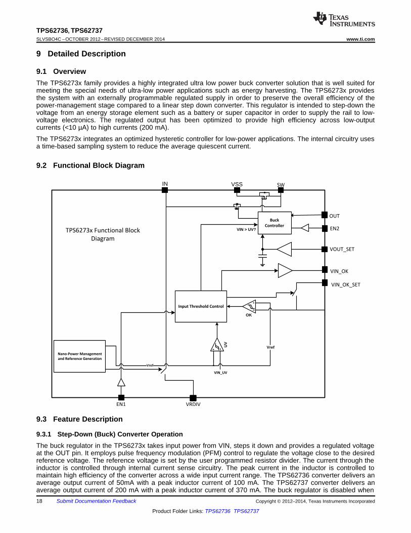
9.1 OverviewThe TPS6273x family provides a highly integrated ultra low power buck converter solution that is well suited formeeting the special needs of ultra-low power applications such as energy harvesting. The TPS6273x providesthe system with an externally programmable regulated supply in order to preserve the overall efficiency of thepower-management stage compared to a linear step down converter. This regulator is intended to step-down thevoltage from an energy storage element such as a battery or super capacitor in order to supply the rail to low-voltage electronics. The regulated output has been optimized to provide high efficiency across low-outputcurrents (<10 µA) to high currents (200 mA).
The TPS6273x integrates an optimized hysteretic controller for low-power applications. The internal circuitry usesa time-based sampling system to reduce the average quiescent current.
9.2 Functional Block Diagram
9.3 Feature Description
9.3.1 Step-Down (Buck) Converter OperationThe buck regulator in the TPS6273x takes input power from VIN, steps it down and provides a regulated voltageat the OUT pin. It employs pulse frequency modulation (PFM) control to regulate the voltage close to the desiredreference voltage. The reference voltage is set by the user programmed resistor divider. The current through theinductor is controlled through internal current sense circuitry. The peak current in the inductor is controlled tomaintain high efficiency of the converter across a wide input current range. The TPS62736 converter delivers anaverage output current of 50mA with a peak inductor current of 100 mA. The TPS62737 converter delivers anaverage output current of 200 mA with a peak inductor current of 370 mA. The buck regulator is disabled when18 Submit Documentation Feedback Copyright © 2012–2014, Texas Instruments Incorporated
Product Folder Links: TPS62736 TPS62737
1 2
1
R RVIN_ OK VBIAS
R
æ ö+= ç ÷
è ø
3 4
4
R RVOUT VBIAS
R
æ ö+= ç ÷
è ø
1 2 3
1
R R RVIN_ OK VBIAS
R
æ ö+ += ç ÷
è ø
1 2 3
1 2
R R RVOUT VBIAS
R R
æ ö+ += ç ÷
+è ø
TPS62736, TPS62737www.ti.com SLVSBO4C –OCTOBER 2012–REVISED DECEMBER 2014
Feature Description (continued)the voltage on VIN reaches the UVLO condition. The UVLO level is continuously monitored. The buck regulatorcontinues to operate in pass (100% duty cycle) mode, passing the input voltage to the output, as long as VIN isgreater than UVLO and less than VIN minus IOUT times RDS(on) of the high-side FET (that is, VIN – IOUT x RDS(on)-HS). In order to save power from being dissipated through other ICs on this supply rail while allowing for a fasterwake up time, the buck regulator can be enabled and disabled through the EN2 pin for systems that desire tocompletely turn off the regulated output.
9.3.2 Programming OUT Regulation Voltage and VIN_OKTo set the proper output-regulation voltage and input voltage power-good comparator, the external resistors mustbe carefully selected. Figure 62 illustrates an application diagram which uses the minimal resistor count forsetting both VOUT and VIN_OK. Note that VBIAS is nominally 1.21 V per the electrical specification table.Referring to Figure 52, the OUT DC set point is given by Equation 1.
(1)
The VIN_OK setting is given by Equation 2.
(2)
The sum of the resistors is recommended to be no greater than 13 MΩ, that is, RSUM = R1 + R2 + R3 = 13 MΩ.Due to the sampling operation of the output resistors, lowering RSUM only increases quiescent current slightly ascan be seen in Figure 22. Higher resistors may result in poor output voltage regulation and/or input voltagepower-good threshold accuracies due to noise pickup through the high-impedance pins or reduction of effectiveresistance due to parasitic resistance created from board assembly residue. See Layout for more details.
If it is preferred to separate the VOUT and VIN_OK resistor strings, two separate strings of resistors could beused as shown in Figure 62. The OUT DC set point is then given by Equation 3.
(3)
The VIN_OK setting is then given by Equation 4.
(4)
If it is preferred to disable the VIN_OK setting, the VIN_OK_SET pin can be tied to VIN. To set VOUT in thisconfiguration, use Equation 3. To tighten the DC set point accuracy, use external resistors with better than 1%resistor tolerance. Because output voltage ripple has a large effect on input line regulation and the output loadregulation, using a larger output capacitor will improve both line and load regulation.
9.3.3 Nano-Power Management and EfficiencyThe high efficiency of the TPS6273x is achieved through the proprietary Nano-Power management circuitry andalgorithm. This feature essentially samples and holds all references in order to reduce the average quiescentcurrent. That is, the internal circuitry is only active for a short period of time and then off for the remaining periodof time at the lowest feasible duty cycle. A portion of this feature can be observed in Figure 66 where the VRDIVnode is monitored. Here, the VRDIV node provides a connection to the input (larger voltage level) and generatesthe output reference (lower-voltage level) for a short period of time. The divided down value of input voltage iscompared to VBIAS and the output voltage reference is sampled and held to get the VOUT_SET point.Because this biases a resistor string, the current through these resistors is only active when the Nano-Powermanagement circuitry makes the connection — hence, reducing the overall quiescent current due to theresistors. This process repeats every 64 ms. Similarly, the VIN_OK level is monitored every 64 ms, as shown inFigure 55.
Copyright © 2012–2014, Texas Instruments Incorporated Submit Documentation Feedback 19
Product Folder Links: TPS62736 TPS62737
TPS62736, TPS62737SLVSBO4C –OCTOBER 2012–REVISED DECEMBER 2014 www.ti.com
Feature Description (continued)The efficiency versus output current and efficiency versus input voltage are plotted for three different outputvoltages for both the TPS62736 and TPS62737 devices in Typical Characteristics. All data points werecaptured by averaging the overall input current. This must be done, due to the periodic biasing schemeimplemented through the Nano-Power management circuitry. The input current efficiency data was gatheredusing a source meter set to average over at least 25 samples and at the highest accuracy sampling rate. Eachdata point takes a long period of time to gather in order to properly measure the resulting input current whencalculating the efficiency.
9.4 Device Functional Modes
9.4.1 Enable ControlsThere are two enable pins implemented in the TPS6273x in order to maximize the flexibility of control for thesystem. The EN1 pin is considered to be the chip enable. If EN1 is set to a 1 then the entire chip is placed intoship mode. If EN1 is 0 then the chip is enabled. EN2 enables and disables the switching of the buck converter.When EN2 is low, the internal circuitry remains ON and the VIN_OK indicator still functions. This can be used todisable down-stream electronics in case of a low input-supply condition. When EN2 is 1, the buck converteroperates normally.
Table 3. Enable Functionality TableEN1 PIN EN2 PIN FUNCTIONAL STATE
0 0 Partial standby mode. Buck switching converter is off, but VIN_OK indication is on0 1 Buck mode and VIN_OK enabled1 x Full standby mode. Switching converter and VIN_OK indication is off (ship mode)
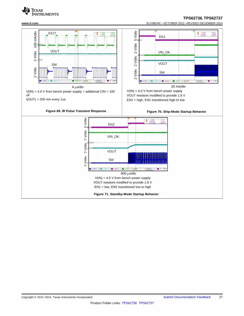
9.4.2 Startup BehaviorThe TPS6273x has two startup responses: 1) from the ship-mode state (EN1 transitions from high to low), and 2)from the standby state (EN2 transitions from low to high). The first startup response out of the ship-mode statehas the longest time duration due to the internal circuitry being disabled. This response is shown in Figure 70 forthe TPS62736 and Figure 60 for the TPS62737. The startup time takes approximately 100 ms due to theinternal Nano-Power management circuitry needing to complete the 64 ms sample and hold cycle.
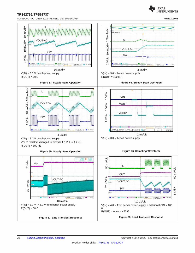
Startup from the standby state is shown in Figure 71 for the TPS62736 and Figure 61 for the TPS62737. Thisresponse is much faster due to the internal circuitry being pre-enabled. The startup time from this state isentirely dependent on the size of the output capacitor. The larger the capacitor, the longer it will take to chargeduring startup. The TPS6273x can startup into a prebiased output voltage.
20 Submit Documentation Feedback Copyright © 2012–2014, Texas Instruments Incorporated
Product Folder Links: TPS62736 TPS62737
System Load
VSS
SWINVIN
CIN1
22PF
10 PHL
Buck
Controller
HostGPIO1
GPIO2 EN1
22PFCOUT
VIN_OK
VRDIV
VIN_OK_SET
R3
R2
VOUT_SET
TPS62737
OUT
GPIO2 EN2
Nano-Power
Management
R1
CIN2
0.1PF
TPS62736, TPS62737www.ti.com SLVSBO4C –OCTOBER 2012–REVISED DECEMBER 2014
10 Application and Implementation
NOTEInformation in the following applications sections is not part of the TI componentspecification, and TI does not warrant its accuracy or completeness. TI’s customers areresponsible for determining suitability of components for their purposes. Customers shouldvalidate and test their design implementation to confirm system functionality.
10.1 Application InformationThe TPS62736/7 are step down DC-DC converters. Their low quiescent currents make them ideal for batterypowered systems that are operated at low duty cycles in order to achieve low total power levels.
10.2 Typical Applications
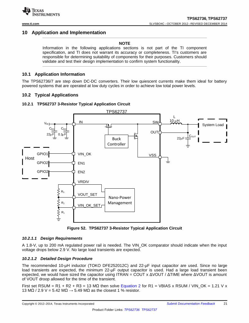
10.2.1 TPS62737 3-Resistor Typical Application Circuit
Figure 52. TPS62737 3-Resistor Typical Application Circuit
10.2.1.1 Design RequirementsA 1.8-V, up to 200 mA regulated power rail is needed. The VIN_OK comparator should indicate when the inputvoltage drops below 2.9 V. No large load transients are expected.
10.2.1.2 Detailed Design ProcedureThe recommended 10-µH inductor (TOKO DFE252012C) and 22-µF input capacitor are used. Since no largeload transients are expected, the minimum 22-µF output capacitor is used. Had a large load transient beenexpected, we would have sized the capacitor using ITRAN = COUT x ΔVOUT / ΔTIME where ΔVOUT is amountof VOUT droop allowed for the time of the transient.
First set RSUM = R1 + R2 + R3 = 13 MΩ then solve Equation 2 for R1 = VBIAS x RSUM / VIN_OK = 1.21 V x13 MΩ / 2.9 V = 5.42 MΩ → 5.49 MΩ as the closest 1 % resistor.
Copyright © 2012–2014, Texas Instruments Incorporated Submit Documentation Feedback 21
Product Folder Links: TPS62736 TPS62737
TPS62736, TPS62737SLVSBO4C –OCTOBER 2012–REVISED DECEMBER 2014 www.ti.com
Typical Applications (continued)Then solve Equation 2 for R2 = VBIAS x RSUM / VOUT - R1 = 1.21 V x 13 MΩ / 1.8 V - 5.42 MΩ = 3.32 MΩ →3.4 MΩ as the closest 1% resistor.
Finally R3 = RSUM - R1 - R2 = 13 MΩ - 5.42 MΩ - 3.32 MΩ = 4.26 MΩ → 4.32 MΩ as the closest 1% resistor.
These values yield VOUT = 1.79 V and VIN_OK threshold = 2.91 V.
If using 4 resistors, see Resistor Selection for guidance on sizing the resistors.
10.2.1.2.1 Inductor Selection
The internal-control circuitry is designed to control the switching behavior with a nominal inductance of 10 µH ±20%. The saturation current of the inductor' should be at least 25% higher than the maximum cycle-by-cyclecurrent limit per the electrical specs table (ILIM) in order to account for load transients. Because this device is ahysteretic controller, it is a naturally stable system (single order transfer function). However, the smaller theinductor value is, the faster the switching currents are. The speed of the peak current detect circuit sets theinductor of the TPS62736 lower bound to 4.7 µH. When using a 4.7 µH, the peak inductor current will increasewhen compared to that of a 10-µH inductor. The steady-state operation with a 4.7-µH inductor with a 50-mA loadfor the TPS62736 is shown in Figure 65.
A list of inductors recommended for this device is shown in Table 4.
Table 4. Recommended InductorsINDUCTANCE (µH) DIMENSIONS (mm) PART NUMBER MANUFACTURER
10 2.0 x 2.5 x 1.2 DFE252012C-H-100M Toko10 4.0 x 4.0 x 1.7 LPS4018-103M Coilcraft
4.7 (TPS62736 only) 2.0 x 2.5 x 1.2 DFE252012R-H-4R7M Toko
10.2.1.2.2 Output Capacitor Selection
The output capacitor is chosen based on transient response behavior and ripple magnitude. The lower thecapacitor value, the larger the ripple will become and the larger the droop will be in the case of a transientresponse. It is recommended to use at least a 22-µF output capacitor for most applications.
10.2.1.2.3 Input Capacitor Selection
The bulk input capacitance is recommended to be a minimum of 4.7 µF ± 20% for the TPS62736 and 22 µF ±20% for the TPS62737. This bulk capacitance is used to suppress the lower frequency transients produced bythe switching converter. There is no upper bound to the input-bulk capacitance. In addition, a high-frequencybypass capacitor of 0.1 µF is recommended in parallel with the bulk capacitor. The high-frequency bypass isused to suppress the high-frequency transients produced by the switching converter.
10.2.1.2.4 Resistor Selection
Equation 1 to Equation 4 are the equations for sizing the external resistors to set the VIN_OK threshold andVOUT regulation value. The spreadsheet at SLVC489 can help size the external resistors.
10.2.1.3 Application CurvesSee efficiency, line regulation, and load regulation curves at Figure 30, Figure 37, and Figure 36.
22 Submit Documentation Feedback Copyright © 2012–2014, Texas Instruments Incorporated
Product Folder Links: TPS62736 TPS62737
2 V
/div
50 m
V/d
iv1 V
/div
200 m
A/d
iv
50 s/divμ
IL
VOUT
VSW
2 V
/div
1 V
/div
100 m
A/d
iv
5 s/divμ
IOUT
VOUT
SW
2 V
/div
2 V
/div
2 V
/div
2 V
/div
100 ms/div
VIN
VIN-OK
VOUT
VRDIV
2 V
/div
50 m
V/d
iv
200 m
A/d
iv200 m
A/d
iv
20 s/divμ
IL
IOUT
VOUT
VSW
2 V
/div
50 m
V/d
iv2
00
mA
V/d
iv
10 s/divμ
IL
SW
VOUT
2 V
1 ms/div
50 m
V200 m
A
50 m
V
1.9
V47.5
mV
190 m
A
47.5
mV
IL
SW
VOUT
VIN
IL
SW
VOUT
VIN
TPS62736, TPS62737www.ti.com SLVSBO4C –OCTOBER 2012–REVISED DECEMBER 2014
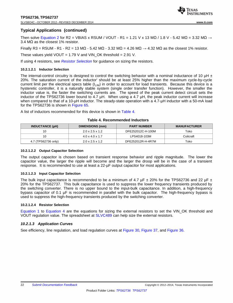
V(IN) = 3.6 V bench power supply V(IN) = 3.6 V bench power supplyR(OUT) = 100 kΩ R(OUT) = 9 Ω
Figure 53. Steady State Operation Figure 54. Steady State Operation
V(IN) = 3.6 V bench power supply + additional C(IN) = 100 uFV(IN) = power amplifier ramped from 0 V to 5 V to 0 VR(OUT) = open to 9 Ω to open
Figure 56. Load Transient ResponseFigure 55. Power Management Response
V(IN) = 4.0 V bench supply + additional C(IN) = 100 uFV(IN) = 3.6 V -> 4.6 V -> 4.6 V from bench power supplyVOUT resistors modified to provide 2.5 VR(OUT) = 9 ΩI(OUT) = 200 mA every 1 us
Figure 58. IR Pulse Transient ResponseFigure 57. Line Transient Response
Copyright © 2012–2014, Texas Instruments Incorporated Submit Documentation Feedback 23
Product Folder Links: TPS62736 TPS62737
2 V
/div
1 V
/div
2 V
/div
2 V
/div
200 s/divμ
EN2VIN-OK
VOUTVSW
2 V
/div
1 V
/div
2 V
/div
2 V
/div
20 ms/div
EN1
VIN-OK
VOUT
VSW
1 V
/div
10 s/div
1 V
/div
1 V
/div
VIN-OK
VOUT
VIN
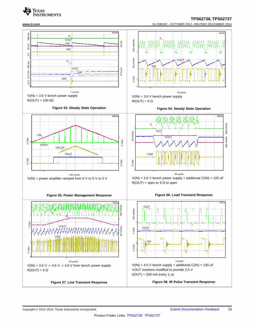
TPS62736, TPS62737SLVSBO4C –OCTOBER 2012–REVISED DECEMBER 2014 www.ti.com
V(IN) = power amplifier ramped from 0 V to 5 V to 0 V V(IN) = 3.6 V bench power supplyEN1 = low; EN2 = high EN2 = high; EN1 transitioned from high to low
R(OUT) = 1 kΩ
Figure 59. Startup Behavior with Slow Ramping Figure 60. Ship-Mode Startup BehaviorVIN
V(IN) = 3.6 V bench power supplyEN1 = low; EN2 transitioned from low to high
R(OUT) = 1 kΩ
Figure 61. Standby-Mode Startup Behavior
24 Submit Documentation Feedback Copyright © 2012–2014, Texas Instruments Incorporated
Product Folder Links: TPS62736 TPS62737
System Load
VSS
SWINVIN
CIN1
4.7PF
10 PHL
Buck
Controller
HostGPIO1
GPIO2 EN1
22PFCOUT
VIN_OK
VRDIV
VIN_OK_SET
R3
R2
VOUT_SET
TPS62736
OUT
GPIO2 EN2
Nano-Power
Management
R1
CIN2
0.1PF
R4
TPS62736, TPS62737www.ti.com SLVSBO4C –OCTOBER 2012–REVISED DECEMBER 2014
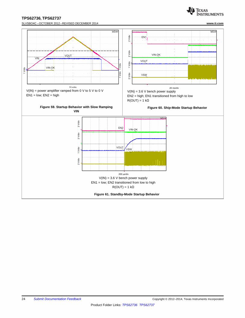
10.2.2 TPS62736 4-Resistor Typical Application Circuit
Figure 62. TPS62736 4-Resistor Typical Application Circuit
10.2.2.1 Design RequirementsA 2.5-V, up to 50-mA regulated power rail is needed. The VIN_OK comparator should indicate when the inputvoltage drops below 2.9 V. No large load transients are expected.
10.2.2.2 Detailed Design ProcedureThe recommended 10-µH inductor (TOKO DFE252012C) and 4.7-µF input capacitor are used. Since no largeload transients are expected, the minimum 22-µF output capacitor is used. Had a large load transient beenexpected, we would have sized the capacitor using ITRAN = COUT x ΔVOUT / ΔTIME where ΔVOUT is amountof VOUT droop allowed for the time of the transient.
First set RSUM = R1 + R2 = R3 + R4 = 13 MΩ then solve Equation 4 for R1 = VBIAS x RSUM / VIN_OK = 1.21V x 13 MΩ / 2.9 V = 5.42 MΩ → 5.36 MΩ as the closest 1 % resistor.
Then R2 = RSUM - R1 = 13 MΩ - 5.42 MΩ = 7.58 MΩ → 7.5 MΩ as the closest 1% resistor.
Solve Equation 3 for R4 = VBIAS x RSUM / VOUT = 1.21 V x 13 MΩ / 2.5 V = 6.29 MΩ → 6.34 MΩ as theclosest 1% resistor.
Finally R3 = RSUM - R3 = 13 MΩ - 6.29 MΩ = 6.71 MΩ → 6.81 MΩ as the closest 1% resistor.
These values yield VOUT = 2.51 V and VIN_OK threshold = 2.90 V.
If using 3 resistors, see Resistor Selection for guidance on sizing the resistors.
10.2.2.3 Application CurvesSee efficiency, load regulation and line regulation graphs at Figure 1, Figure 7 and Figure 8 respectively.
Copyright © 2012–2014, Texas Instruments Incorporated Submit Documentation Feedback 25
Product Folder Links: TPS62736 TPS62737
5 V
/div
50 m
A/d
iv
10 Ps/div
20 m
V/d
iv 50 m
A/d
iv
VOUT-AC
SW
IOUT
IL
10 m
V/d
iv2
V/d
iv
40 ms/div
VIN
VOUT-AC
2 V
/div
10 m
V/d
iv10
0 m
A/d
iv
4 Ps/div
VOUT-AC
IL
SW
1 V
/div
1 V
/div
1 V
/div
2 ms/div
VRDIV
VOUT
VIN
VOUT-AC
SW
IL2
V/d
iv10
mV
/div
50 m
A/d
iv
10 Ps/div
2 V
/div
10 m
V/d
iv10
0 m
A/d
iv
2 Ps/div
IL
VOUT-AC
SW
TPS62736, TPS62737SLVSBO4C –OCTOBER 2012–REVISED DECEMBER 2014 www.ti.com
V(IN) = 3.0 V bench power supply V(IN) = 3.0 V bench power supplyR(OUT) = 50 Ω R(OUT) = 100 kΩ
Figure 63. Steady State Operation Figure 64. Steady State Operation
V(IN) = 3.0 V bench power supplyV(IN) = 3.0 V bench power supplyVOUT resistors changed to provide 1.8 V; L = 4.7 uHR(OUT) = 100 kΩ
Figure 66. Sampling WaveformFigure 65. Steady State Operation
V(IN) = 3.0 V -> 5.0 V from bench power supply V(IN) = 4.0 V from bench power supply + additional CIN = 100uFR(OUT) = 50 ΩR(OUT) = open - > 50 Ω
Figure 68. Load Transient ResponseFigure 67. Line Transient Response
26 Submit Documentation Feedback Copyright © 2012–2014, Texas Instruments Incorporated
Product Folder Links: TPS62736 TPS62737
2 V
/div
5 V
/div
400 Ps/div
2 V
/div
2 V
/div
VOUT
SW
VIN_OK
EN2
2 V
/div
100
mA
/div
4 Ps/div
2 V
/div VOUT
IOUT
SW
2 V
/div
5 V
/div
20 ms/div
2 V
/div
VOUT
SW
VIN_OK
EN1
2 V
/div
TPS62736, TPS62737www.ti.com SLVSBO4C –OCTOBER 2012–REVISED DECEMBER 2014
V(IN) = 4.0 V from bench power supplyV(IN) = 4.0 V from bench power supply + additional CIN = 100uF VOUT resistors modified to provide 1.8 VI(OUT) = 200 mA every 1us EN2 = high, EN1 transitioned high to low
Figure 69. IR Pulse Transient Response Figure 70. Ship-Mode Startup Behavior
V(IN) = 4.0 V from bench power supplyVOUT resistors modified to provide 1.8 VEN1 = low, EN2 transitioned low to high
Figure 71. Standby-Mode Startup Behavior
Copyright © 2012–2014, Texas Instruments Incorporated Submit Documentation Feedback 27
Product Folder Links: TPS62736 TPS62737
VIAS to GND PLANE
VIN
VOUT
CIN1
CIN2
COUTL1
R1R2R3
1
VIA toGND PLANE
VIAS toGND PLANE
VIN
VOUT
CIN1
CIN2
COUTL1
R1R2R3
1
VIA to GND PLANE
VIAS toGND PLANE
TPS62736, TPS62737SLVSBO4C –OCTOBER 2012–REVISED DECEMBER 2014 www.ti.com
11 Power Supply RecommendationsThe TPS62736 / 7 ICs require a low impedance power source (e.g. battery, wall adapter) capable of providngbetween 2.0 V and 5.5 V and up to 100 mA / 370 mA respectively. When the voltage at IN is less than or equalto VOUT, the IC stops switching, turns on the high side FET and provides VOUT = VIN - ILOAD x RDS(on)-HighSideFET.
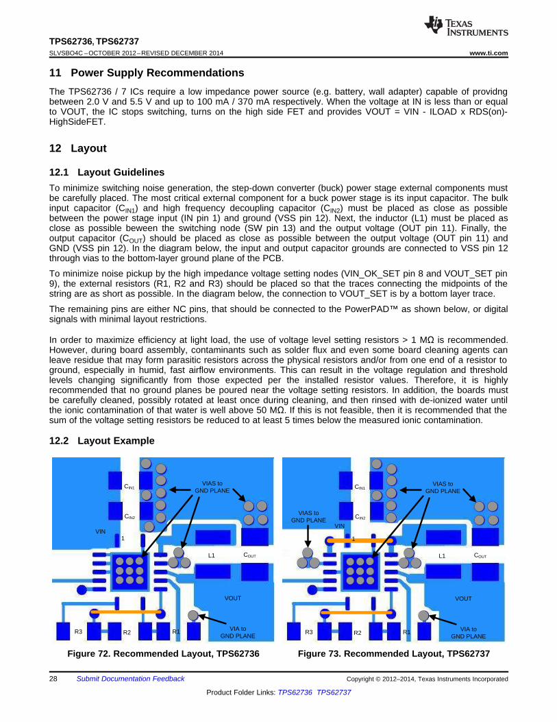
12 Layout
12.1 Layout GuidelinesTo minimize switching noise generation, the step-down converter (buck) power stage external components mustbe carefully placed. The most critical external component for a buck power stage is its input capacitor. The bulkinput capacitor (CIN1) and high frequency decoupling capacitor (CIN2) must be placed as close as possiblebetween the power stage input (IN pin 1) and ground (VSS pin 12). Next, the inductor (L1) must be placed asclose as possible beween the switching node (SW pin 13) and the output voltage (OUT pin 11). Finally, theoutput capacitor (COUT) should be placed as close as possible between the output voltage (OUT pin 11) andGND (VSS pin 12). In the diagram below, the input and output capacitor grounds are connected to VSS pin 12through vias to the bottom-layer ground plane of the PCB.
To minimize noise pickup by the high impedance voltage setting nodes (VIN_OK_SET pin 8 and VOUT_SET pin9), the external resistors (R1, R2 and R3) should be placed so that the traces connecting the midpoints of thestring are as short as possible. In the diagram below, the connection to VOUT_SET is by a bottom layer trace.
The remaining pins are either NC pins, that should be connected to the PowerPAD™ as shown below, or digitalsignals with minimal layout restrictions.
In order to maximize efficiency at light load, the use of voltage level setting resistors > 1 MΩ is recommended.However, during board assembly, contaminants such as solder flux and even some board cleaning agents canleave residue that may form parasitic resistors across the physical resistors and/or from one end of a resistor toground, especially in humid, fast airflow environments. This can result in the voltage regulation and thresholdlevels changing significantly from those expected per the installed resistor values. Therefore, it is highlyrecommended that no ground planes be poured near the voltage setting resistors. In addition, the boards mustbe carefully cleaned, possibly rotated at least once during cleaning, and then rinsed with de-ionized water untilthe ionic contamination of that water is well above 50 MΩ. If this is not feasible, then it is recommended that thesum of the voltage setting resistors be reduced to at least 5 times below the measured ionic contamination.
12.2 Layout Example
Figure 72. Recommended Layout, TPS62736 Figure 73. Recommended Layout, TPS62737
28 Submit Documentation Feedback Copyright © 2012–2014, Texas Instruments Incorporated
Product Folder Links: TPS62736 TPS62737
TPS62736, TPS62737www.ti.com SLVSBO4C –OCTOBER 2012–REVISED DECEMBER 2014
13 Device and Documentation Support
13.1 Device Support
13.1.1 Third-Party Products DisclaimerTI'S PUBLICATION OF INFORMATION REGARDING THIRD-PARTY PRODUCTS OR SERVICES DOES NOTCONSTITUTE AN ENDORSEMENT REGARDING THE SUITABILITY OF SUCH PRODUCTS OR SERVICESOR A WARRANTY, REPRESENTATION OR ENDORSEMENT OF SUCH PRODUCTS OR SERVICES, EITHERALONE OR IN COMBINATION WITH ANY TI PRODUCT OR SERVICE.
13.2 Related LinksThe table below lists quick access links. Categories include technical documents, support and communityresources, tools and software, and quick access to sample or buy.
Table 5. Related LinksTECHNICAL TOOLS & SUPPORT &PARTS PRODUCT FOLDER SAMPLE & BUY DOCUMENTS SOFTWARE COMMUNITY
TPS62736 Click here Click here Click here Click here Click hereTPS62737 Click here Click here Click here Click here Click here
13.3 TrademarksPowerPAD is a trademark of Texas Instruments.All other trademarks are the property of their respective owners.
13.4 Electrostatic Discharge CautionThese devices have limited built-in ESD protection. The leads should be shorted together or the device placed in conductive foamduring storage or handling to prevent electrostatic damage to the MOS gates.
13.5 GlossarySLYZ022 — TI Glossary.
This glossary lists and explains terms, acronyms, and definitions.
14 Mechanical, Packaging, and Orderable InformationThe following pages include mechanical, packaging, and orderable information. This information is the mostcurrent data available for the designated devices. This data is subject to change without notice and revision ofthis document. For browser-based versions of this data sheet, refer to the left-hand navigation.
Copyright © 2012–2014, Texas Instruments Incorporated Submit Documentation Feedback 29
Product Folder Links: TPS62736 TPS62737
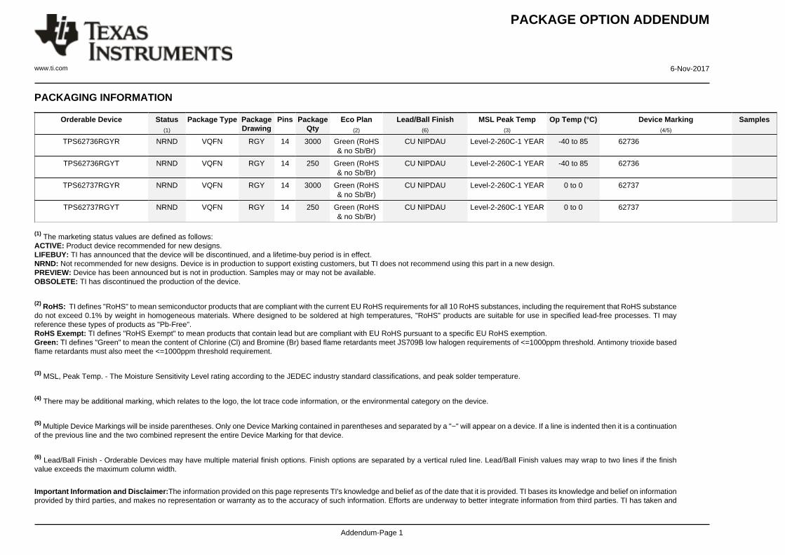
PACKAGE OPTION ADDENDUM
www.ti.com 6-Nov-2017
Addendum-Page 1
PACKAGING INFORMATION
Orderable Device Status(1)
Package Type PackageDrawing
Pins PackageQty
Eco Plan(2)
Lead/Ball Finish(6)
MSL Peak Temp(3)
Op Temp (°C) Device Marking(4/5)
Samples
TPS62736RGYR NRND VQFN RGY 14 3000 Green (RoHS& no Sb/Br)
CU NIPDAU Level-2-260C-1 YEAR -40 to 85 62736
TPS62736RGYT NRND VQFN RGY 14 250 Green (RoHS& no Sb/Br)
CU NIPDAU Level-2-260C-1 YEAR -40 to 85 62736
TPS62737RGYR NRND VQFN RGY 14 3000 Green (RoHS& no Sb/Br)
CU NIPDAU Level-2-260C-1 YEAR 0 to 0 62737
TPS62737RGYT NRND VQFN RGY 14 250 Green (RoHS& no Sb/Br)
CU NIPDAU Level-2-260C-1 YEAR 0 to 0 62737
(1) The marketing status values are defined as follows:ACTIVE: Product device recommended for new designs.LIFEBUY: TI has announced that the device will be discontinued, and a lifetime-buy period is in effect.NRND: Not recommended for new designs. Device is in production to support existing customers, but TI does not recommend using this part in a new design.PREVIEW: Device has been announced but is not in production. Samples may or may not be available.OBSOLETE: TI has discontinued the production of the device.
(2) RoHS: TI defines "RoHS" to mean semiconductor products that are compliant with the current EU RoHS requirements for all 10 RoHS substances, including the requirement that RoHS substancedo not exceed 0.1% by weight in homogeneous materials. Where designed to be soldered at high temperatures, "RoHS" products are suitable for use in specified lead-free processes. TI mayreference these types of products as "Pb-Free".RoHS Exempt: TI defines "RoHS Exempt" to mean products that contain lead but are compliant with EU RoHS pursuant to a specific EU RoHS exemption.Green: TI defines "Green" to mean the content of Chlorine (Cl) and Bromine (Br) based flame retardants meet JS709B low halogen requirements of <=1000ppm threshold. Antimony trioxide basedflame retardants must also meet the <=1000ppm threshold requirement.
(3) MSL, Peak Temp. - The Moisture Sensitivity Level rating according to the JEDEC industry standard classifications, and peak solder temperature.
(4) There may be additional marking, which relates to the logo, the lot trace code information, or the environmental category on the device.
(5) Multiple Device Markings will be inside parentheses. Only one Device Marking contained in parentheses and separated by a "~" will appear on a device. If a line is indented then it is a continuationof the previous line and the two combined represent the entire Device Marking for that device.
(6) Lead/Ball Finish - Orderable Devices may have multiple material finish options. Finish options are separated by a vertical ruled line. Lead/Ball Finish values may wrap to two lines if the finishvalue exceeds the maximum column width.
Important Information and Disclaimer:The information provided on this page represents TI's knowledge and belief as of the date that it is provided. TI bases its knowledge and belief on informationprovided by third parties, and makes no representation or warranty as to the accuracy of such information. Efforts are underway to better integrate information from third parties. TI has taken and
PACKAGE OPTION ADDENDUM
www.ti.com 6-Nov-2017
Addendum-Page 2
continues to take reasonable steps to provide representative and accurate information but may not have conducted destructive testing or chemical analysis on incoming materials and chemicals.TI and TI suppliers consider certain information to be proprietary, and thus CAS numbers and other limited information may not be available for release.
In no event shall TI's liability arising out of such information exceed the total purchase price of the TI part(s) at issue in this document sold by TI to Customer on an annual basis.
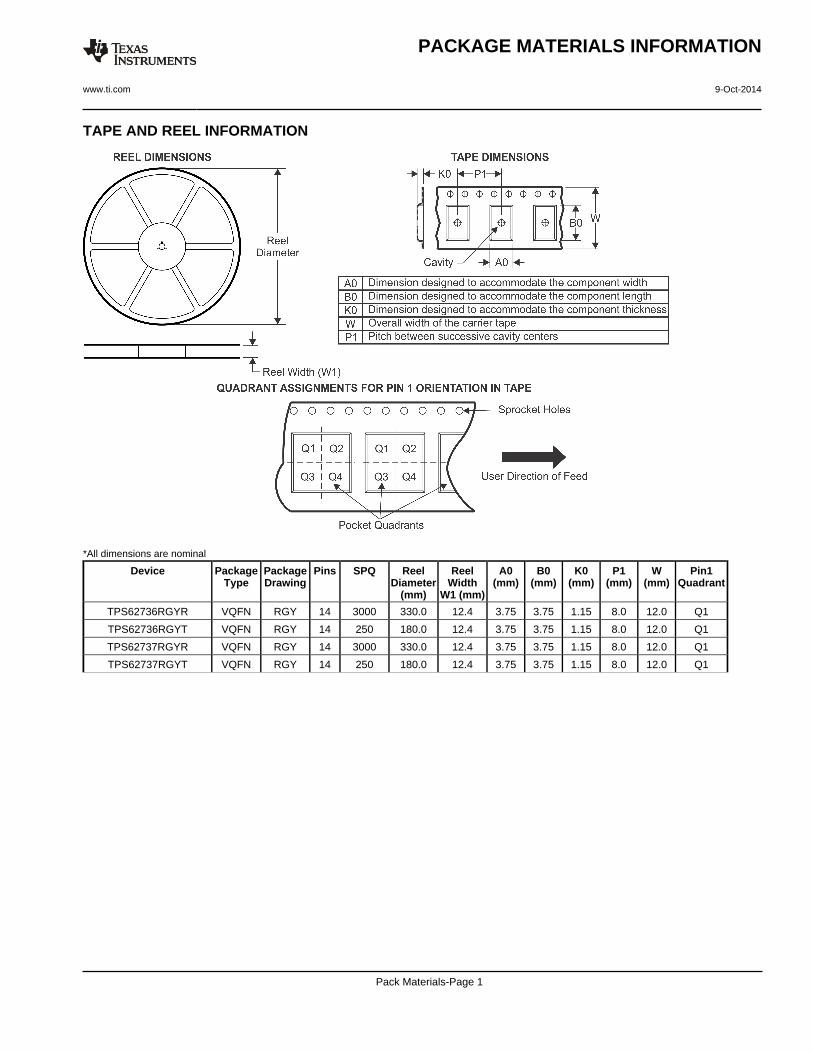
TAPE AND REEL INFORMATION
*All dimensions are nominal
Device PackageType
PackageDrawing
Pins SPQ ReelDiameter
(mm)
ReelWidth
W1 (mm)
A0(mm)
B0(mm)
K0(mm)
P1(mm)
W(mm)
Pin1Quadrant
TPS62736RGYR VQFN RGY 14 3000 330.0 12.4 3.75 3.75 1.15 8.0 12.0 Q1
TPS62736RGYT VQFN RGY 14 250 180.0 12.4 3.75 3.75 1.15 8.0 12.0 Q1
TPS62737RGYR VQFN RGY 14 3000 330.0 12.4 3.75 3.75 1.15 8.0 12.0 Q1
TPS62737RGYT VQFN RGY 14 250 180.0 12.4 3.75 3.75 1.15 8.0 12.0 Q1
PACKAGE MATERIALS INFORMATION
www.ti.com 9-Oct-2014
Pack Materials-Page 1
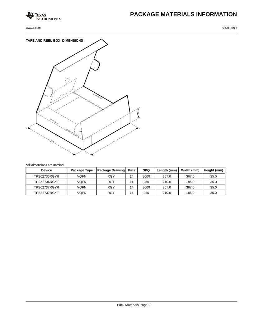
*All dimensions are nominal
Device Package Type Package Drawing Pins SPQ Length (mm) Width (mm) Height (mm)
TPS62736RGYR VQFN RGY 14 3000 367.0 367.0 35.0
TPS62736RGYT VQFN RGY 14 250 210.0 185.0 35.0
TPS62737RGYR VQFN RGY 14 3000 367.0 367.0 35.0
TPS62737RGYT VQFN RGY 14 250 210.0 185.0 35.0
PACKAGE MATERIALS INFORMATION
www.ti.com 9-Oct-2014
Pack Materials-Page 2
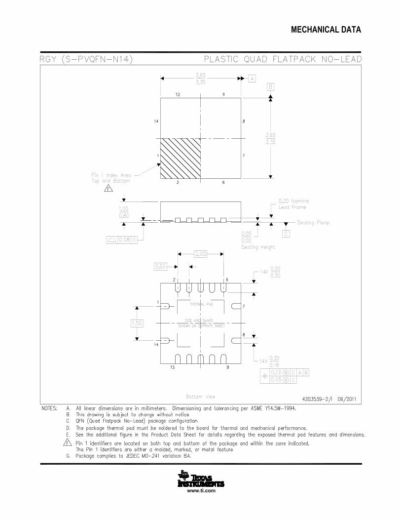
IMPORTANT NOTICE
Texas Instruments Incorporated (TI) reserves the right to make corrections, enhancements, improvements and other changes to itssemiconductor products and services per JESD46, latest issue, and to discontinue any product or service per JESD48, latest issue. Buyersshould obtain the latest relevant information before placing orders and should verify that such information is current and complete.TI’s published terms of sale for semiconductor products (http://www.ti.com/sc/docs/stdterms.htm) apply to the sale of packaged integratedcircuit products that TI has qualified and released to market. Additional terms may apply to the use or sale of other types of TI products andservices.Reproduction of significant portions of TI information in TI data sheets is permissible only if reproduction is without alteration and isaccompanied by all associated warranties, conditions, limitations, and notices. TI is not responsible or liable for such reproduceddocumentation. Information of third parties may be subject to additional restrictions. Resale of TI products or services with statementsdifferent from or beyond the parameters stated by TI for that product or service voids all express and any implied warranties for theassociated TI product or service and is an unfair and deceptive business practice. TI is not responsible or liable for any such statements.Buyers and others who are developing systems that incorporate TI products (collectively, “Designers”) understand and agree that Designersremain responsible for using their independent analysis, evaluation and judgment in designing their applications and that Designers havefull and exclusive responsibility to assure the safety of Designers' applications and compliance of their applications (and of all TI productsused in or for Designers’ applications) with all applicable regulations, laws and other applicable requirements. Designer represents that, withrespect to their applications, Designer has all the necessary expertise to create and implement safeguards that (1) anticipate dangerousconsequences of failures, (2) monitor failures and their consequences, and (3) lessen the likelihood of failures that might cause harm andtake appropriate actions. Designer agrees that prior to using or distributing any applications that include TI products, Designer willthoroughly test such applications and the functionality of such TI products as used in such applications.TI’s provision of technical, application or other design advice, quality characterization, reliability data or other services or information,including, but not limited to, reference designs and materials relating to evaluation modules, (collectively, “TI Resources”) are intended toassist designers who are developing applications that incorporate TI products; by downloading, accessing or using TI Resources in anyway, Designer (individually or, if Designer is acting on behalf of a company, Designer’s company) agrees to use any particular TI Resourcesolely for this purpose and subject to the terms of this Notice.TI’s provision of TI Resources does not expand or otherwise alter TI’s applicable published warranties or warranty disclaimers for TIproducts, and no additional obligations or liabilities arise from TI providing such TI Resources. TI reserves the right to make corrections,enhancements, improvements and other changes to its TI Resources. TI has not conducted any testing other than that specificallydescribed in the published documentation for a particular TI Resource.Designer is authorized to use, copy and modify any individual TI Resource only in connection with the development of applications thatinclude the TI product(s) identified in such TI Resource. NO OTHER LICENSE, EXPRESS OR IMPLIED, BY ESTOPPEL OR OTHERWISETO ANY OTHER TI INTELLECTUAL PROPERTY RIGHT, AND NO LICENSE TO ANY TECHNOLOGY OR INTELLECTUAL PROPERTYRIGHT OF TI OR ANY THIRD PARTY IS GRANTED HEREIN, including but not limited to any patent right, copyright, mask work right, orother intellectual property right relating to any combination, machine, or process in which TI products or services are used. Informationregarding or referencing third-party products or services does not constitute a license to use such products or services, or a warranty orendorsement thereof. Use of TI Resources may require a license from a third party under the patents or other intellectual property of thethird party, or a license from TI under the patents or other intellectual property of TI.TI RESOURCES ARE PROVIDED “AS IS” AND WITH ALL FAULTS. TI DISCLAIMS ALL OTHER WARRANTIES ORREPRESENTATIONS, EXPRESS OR IMPLIED, REGARDING RESOURCES OR USE THEREOF, INCLUDING BUT NOT LIMITED TOACCURACY OR COMPLETENESS, TITLE, ANY EPIDEMIC FAILURE WARRANTY AND ANY IMPLIED WARRANTIES OFMERCHANTABILITY, FITNESS FOR A PARTICULAR PURPOSE, AND NON-INFRINGEMENT OF ANY THIRD PARTY INTELLECTUALPROPERTY RIGHTS. TI SHALL NOT BE LIABLE FOR AND SHALL NOT DEFEND OR INDEMNIFY DESIGNER AGAINST ANY CLAIM,INCLUDING BUT NOT LIMITED TO ANY INFRINGEMENT CLAIM THAT RELATES TO OR IS BASED ON ANY COMBINATION OFPRODUCTS EVEN IF DESCRIBED IN TI RESOURCES OR OTHERWISE. IN NO EVENT SHALL TI BE LIABLE FOR ANY ACTUAL,DIRECT, SPECIAL, COLLATERAL, INDIRECT, PUNITIVE, INCIDENTAL, CONSEQUENTIAL OR EXEMPLARY DAMAGES INCONNECTION WITH OR ARISING OUT OF TI RESOURCES OR USE THEREOF, AND REGARDLESS OF WHETHER TI HAS BEENADVISED OF THE POSSIBILITY OF SUCH DAMAGES.Unless TI has explicitly designated an individual product as meeting the requirements of a particular industry standard (e.g., ISO/TS 16949and ISO 26262), TI is not responsible for any failure to meet such industry standard requirements.Where TI specifically promotes products as facilitating functional safety or as compliant with industry functional safety standards, suchproducts are intended to help enable customers to design and create their own applications that meet applicable functional safety standardsand requirements. Using products in an application does not by itself establish any safety features in the application. Designers mustensure compliance with safety-related requirements and standards applicable to their applications. Designer may not use any TI products inlife-critical medical equipment unless authorized officers of the parties have executed a special contract specifically governing such use.Life-critical medical equipment is medical equipment where failure of such equipment would cause serious bodily injury or death (e.g., lifesupport, pacemakers, defibrillators, heart pumps, neurostimulators, and implantables). Such equipment includes, without limitation, allmedical devices identified by the U.S. Food and Drug Administration as Class III devices and equivalent classifications outside the U.S.TI may expressly designate certain products as completing a particular qualification (e.g., Q100, Military Grade, or Enhanced Product).Designers agree that it has the necessary expertise to select the product with the appropriate qualification designation for their applicationsand that proper product selection is at Designers’ own risk. Designers are solely responsible for compliance with all legal and regulatoryrequirements in connection with such selection.Designer will fully indemnify TI and its representatives against any damages, costs, losses, and/or liabilities arising out of Designer’s non-compliance with the terms and provisions of this Notice.
Mailing Address: Texas Instruments, Post Office Box 655303, Dallas, Texas 75265Copyright © 2017, Texas Instruments Incorporated