Embed Size (px)
Citation preview
1
Programmable Solid State 12AX7 Triode Gain Stage
By: Ian Campbell
Senior Project
Advisor: Dr. Wayne Pilkington
ELECTRICAL ENGINEERING DEPARTMENT
California Polytechnic State University
San Luis Obispo
2011
2
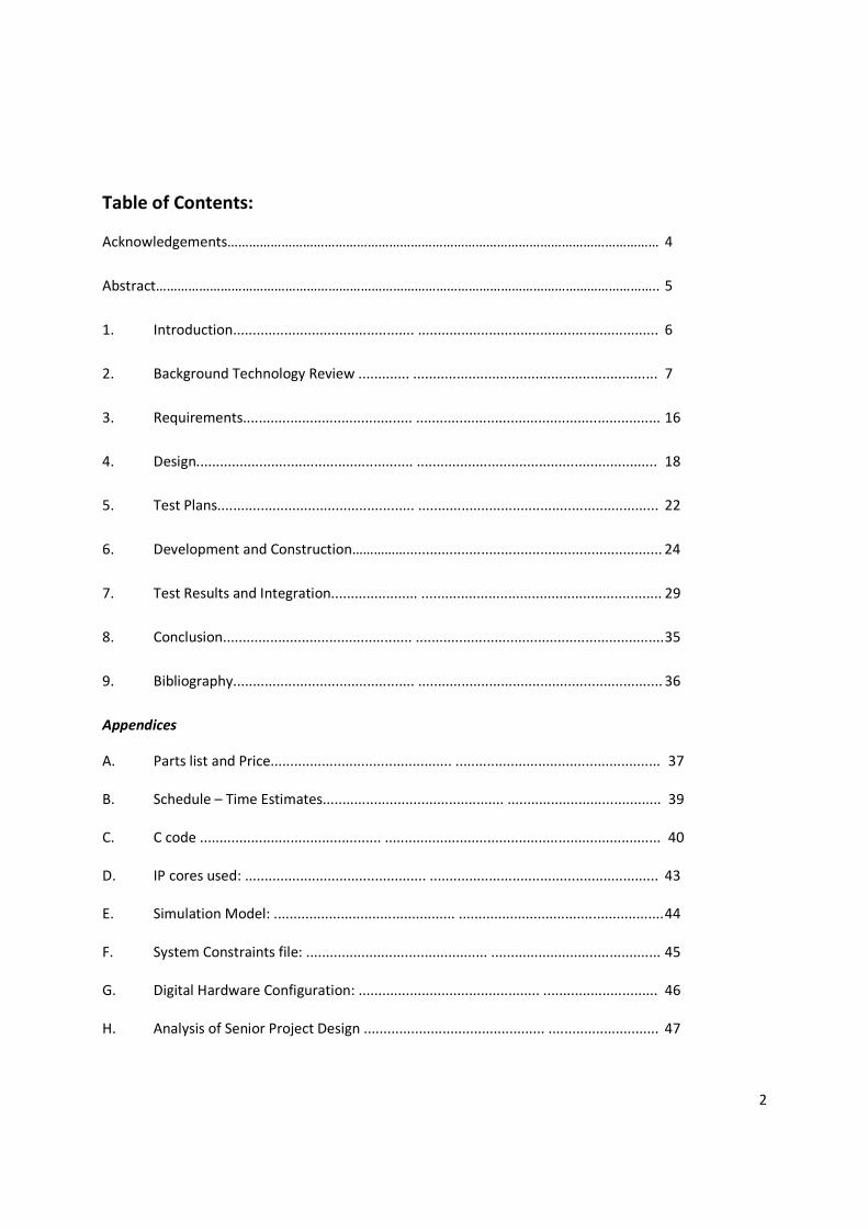
Table of Contents:
Acknowledgements………………………………………………………………………………………………………… 4
Abstract………………………………………………………………………………………………………………………….. 5
1. Introduction.............................................. ............................................................. 6
2. Background Technology Review ............. .............................................................. 7
3. Requirements........................................... .............................................................. 16
4. Design....................................................... ............................................................. 18
5. Test Plans.................................................. ............................................................. 22
6. Development and Construction……………................................................................. 24
7. Test Results and Integration...................... ............................................................. 29
8. Conclusion................................................ ............................................................... 35
9. Bibliography.............................................. .............................................................. 36
Appendices
A. Parts list and Price.............................................. .................................................... 37
B. Schedule – Time Estimates.............................................. ....................................... 39
C. C code .............................................. ...................................................................... 40
D. IP cores used: .............................................. .......................................................... 43
E. Simulation Model: .............................................. .................................................... 44
F. System Constraints file: .............................................. ........................................... 45
G. Digital Hardware Configuration: .............................................. ............................. 46
H. Analysis of Senior Project Design .............................................. ............................ 47
3
List of Tables and/or Figures
Table
1. Table 3.1: Sub-System Level Requirements: …………………………………………………… 17
2. Table 7.1: Linear Gain Numbers with frequency for High Voltage Gain Stage…… 31
3. Table 7.2: Low Pass Level Shifter Frequency Response…………………………………….. 32
Figures:
1. Figure 2.1: Average Transfer Characteristics of 12AX7 in triode operations ……………. 8
2. Figure 2.2: LT Spice Schematic of Common Cathode Gain Stage………………………………. 9
3. Figure 2.3: LT Spice Transient simulation of Cathode. …………………………………………….. 9
4. Figure 2.4: LT Spice Fast Fourier Transform output of Common Cathode gain stage… 10
5. Figure 2.5: LT Spice AC analysis of Common Cathode gain stage. ……………………………. 11
6. Figure 2.6: Fender Champ Schematic (Model 5F1) …………………………………………………… 12
7. Figure 2.7: Breaking the Triode Gain Stage with the Simulator. ……………………………. 13
8. Figure 2.8: System Level Block diagram……………………………. …………………………………… 14
9. Figure 2.9: Total Harmonic Distortion and Noise seen in OPA2277. ………………………… 15
10. Figure 2.10: THD and Noise as seen in OPA445 High Voltage Op-Amp. ………………… 16
11. Figure 4.1: Level Shifting Low Pass Filter…………………………….…………………………….…. 19
12. Figure 4.2: Inverting Amplifier…………………………….…………………………….………………… 20
13. Figure 4.3: Scaled Transfer Function of Tube as Digital points in 12 bits. ……………… 22
14. Figure 6.1: Low Pass Level shifter construction and wiring. ………………………………….. 25
15. Figure 6.2: High Voltage Op-Amp Gain Stage…………………………….…………………………… 25
16. Figure 6.3: Nexys2 with PMod DAC and ADC…………………………….………………………….. 26
17. Figure 6.4: Champ power supply detail. …………………………….………………………………… 26
18. Figure 6.5: Champ Power Supply…………………………….…………………………….……………… 27
19. Figure 6.6: 12AX7 Pinout Box…………………………….…………………………….……………………. 27
4
20. Figure 6.7: 6V6 Pinout Box…………………………….…………………………….………………………… 28
21. Figure 6.8: Breadboard-ed Passive Components for Champ……………….…………………… 28
22. Figure 6.9: Output tube Speaker and connections. …………………………….………………… 29
23. Figure 7.1: Photo of Operational System. …………………………….……………………………….. 30
24. Figure 7.2: Gain of High Voltage Amp. …………………………….……………………………………. 31
25. Figure 7.3: Detail of output kink on OPA445 output at 14kHz. ………………………………. 32
26. Figure 7.4: Analog Activity of Low Pass Level Shifter. …………………………….……………… 33
27. Figure 7.5: Comparison of altered gain stage 1 ………………………………………………….... 34
28. Figure 7.6: Comparison of altered gain stage 2 ……………………………………………………. 34

5
Acknowledgements: Thanks to Dr. Pilkington for allowing me to take on this project. Thanks are also due to so many more
who have accepted and encouraged my desire to tinker, test, design and play. They are too many to list
here. Of these the most deserving of mention are my parents who have tolerated the electrical clutter
that has followed me around for the last few years. Thanks mom and sorry about the mess!
6
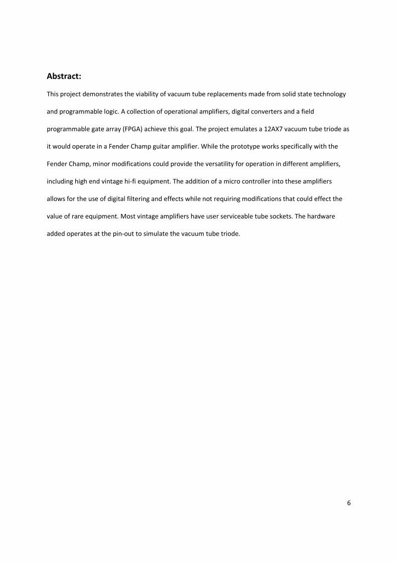
Abstract:
This project demonstrates the viability of vacuum tube replacements made from solid state technology
and programmable logic. A collection of operational amplifiers, digital converters and a field
programmable gate array (FPGA) achieve this goal. The project emulates a 12AX7 vacuum tube triode as
it would operate in a Fender Champ guitar amplifier. While the prototype works specifically with the
Fender Champ, minor modifications could provide the versatility for operation in different amplifiers,
including high end vintage hi-fi equipment. The addition of a micro controller into these amplifiers
allows for the use of digital filtering and effects while not requiring modifications that could effect the
value of rare equipment. Most vintage amplifiers have user serviceable tube sockets. The hardware
added operates at the pin-out to simulate the vacuum tube triode.
7
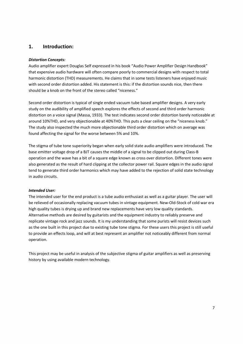
1. Introduction:
Distortion Concepts: Audio amplifier expert Douglas Self expressed in his book “Audio Power Amplifier Design Handbook”
that expensive audio hardware will often compare poorly to commercial designs with respect to total
harmonic distortion (THD) measurements. He claims that in some tests listeners have enjoyed music
with second order distortion added. His statement is this: if the distortion sounds nice, then there
should be a knob on the front of the stereo called “niceness.”
Second order distortion is typical of single ended vacuum tube based amplifier designs. A very early
study on the audibility of amplified speech explores the effects of second and third order harmonic
distortion on a voice signal (Massa, 1933). The test indicates second order distortion barely noticeable at
around 10%THD, and very objectionable at 40%THD. This puts a clear ceiling on the “niceness knob.”
The study also inspected the much more objectionable third order distortion which on average was
found affecting the signal for the worse between 5% and 10%.
The stigma of tube tone superiority began when early solid state audio amplifiers were introduced. The
base emitter voltage drop of a BJT causes the middle of a signal to be clipped out during Class-B
operation and the wave has a bit of a square edge known as cross over distortion. Different tones were
also generated as the result of hard clipping at the collector power rail. Square edges in the audio signal
tend to generate third order harmonics which may have added to the rejection of solid state technology
in audio circuits.
Intended User:
The intended user for the end product is a tube audio enthusiast as well as a guitar player. The user will
be relieved of occasionally replacing vacuum tubes in vintage equipment. New-Old-Stock of cold war era
high quality tubes is drying up and brand new replacements have very low quality standards.
Alternative methods are desired by guitarists and the equipment industry to reliably preserve and
replicate vintage rock and jazz sounds. It is my understanding that some purists will resist devices such
as the one built in this project due to existing tube tone stigma. For these users this project is still useful
to provide an effects loop, and will at best represent an amplifier not noticeably different from normal
operation.
This project may be useful in analysis of the subjective stigma of guitar amplifiers as well as preserving
history by using available modern technology.
8
2. Background Technology Review:
The research and development below are organized by system level activity as well as subsystem
behavior.
The 12AX7 and Other Tubes:
The pre amp tube used in the Fender Champ is a 12AX7. Most tube guitar amps employ this tube and
the remaining tube manufacturers all produce a 12AX7 model. This keeps the cost low. The main
concerns of working with this or any other vacuum tube is safety. The champ operates the cathode plate
of the first and second triodes at 160V and 206V respectively. The 6V6 power tube operates at 305 volts
DC. These are large and dangerous voltages. 12AX7s also have a center tapped 12.6V heater which can
be set with 6.3 volts on either side. This means a high current 6.3V AC tap is required to come from the
power supply. Initial plans outlined regulating the high voltage supply and using it to power the solid
state hardware. While this still seems a viable option issues of cross regulation as well as safety caused
this goal to be abandoned.
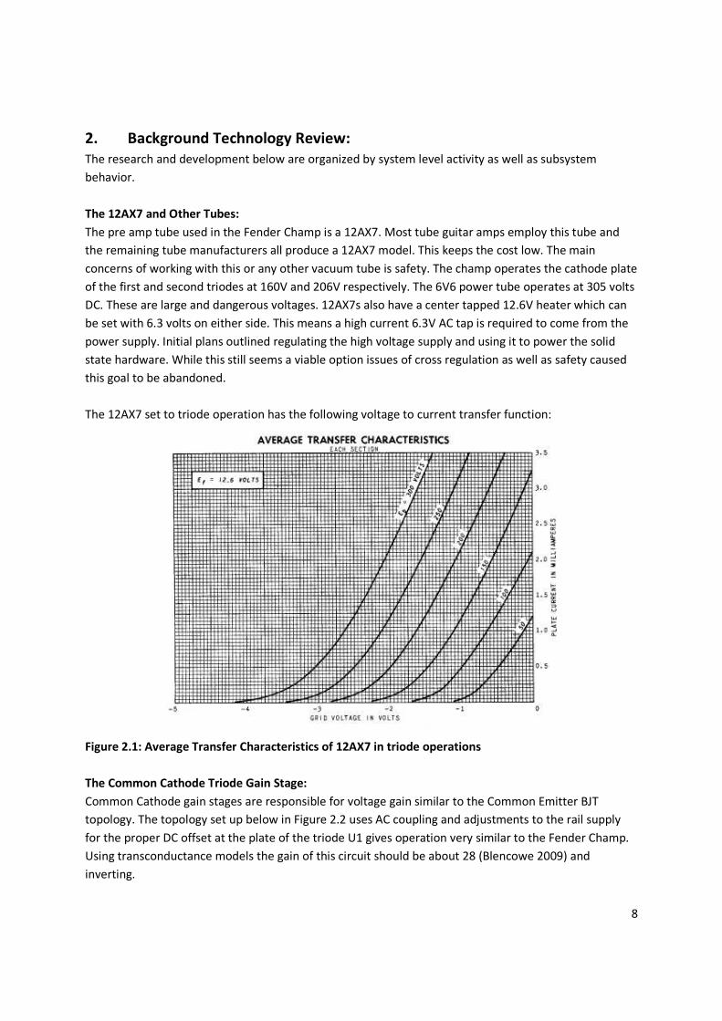
The 12AX7 set to triode operation has the following voltage to current transfer function:
Figure 2.1: Average Transfer Characteristics of 12AX7 in triode operations
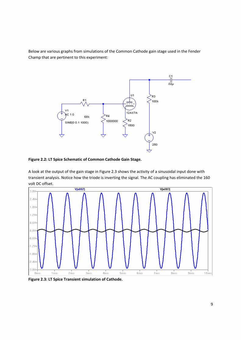
The Common Cathode Triode Gain Stage:
Common Cathode gain stages are responsible for voltage gain similar to the Common Emitter BJT
topology. The topology set up below in Figure 2.2 uses AC coupling and adjustments to the rail supply
for the proper DC offset at the plate of the triode U1 gives operation very similar to the Fender Champ.
Using transconductance models the gain of this circuit should be about 28 (Blencowe 2009) and
inverting.
9
Below are various graphs from simulations of the Common Cathode gain stage used in the Fender
Champ that are pertinent to this experiment:
Figure 2.2: LT Spice Schematic of Common Cathode Gain Stage.
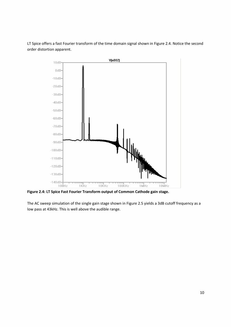
A look at the output of the gain stage in Figure 2.3 shows the activity of a sinusoidal input done with
transient analysis. Notice how the triode is inverting the signal. The AC coupling has eliminated the 160
volt DC offset.
Figure 2.3: LT Spice Transient simulation of Cathode.
10
LT Spice offers a fast Fourier transform of the time domain signal shown in Figure 2.4. Notice the second
order distortion apparent.
Figure 2.4: LT Spice Fast Fourier Transform output of Common Cathode gain stage.
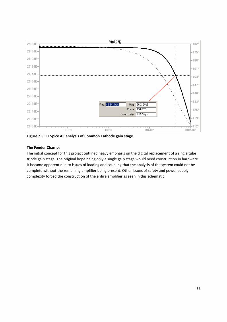
The AC sweep simulation of the single gain stage shown in Figure 2.5 yields a 3dB cutoff frequency as a
low pass at 43kHz. This is well above the audible range.
11
Figure 2.5: LT Spice AC analysis of Common Cathode gain stage.
The Fender Champ: The initial concept for this project outlined heavy emphasis on the digital replacement of a single tube
triode gain stage. The original hope being only a single gain stage would need construction in hardware.
It became apparent due to issues of loading and coupling that the analysis of the system could not be
complete without the remaining amplifier being present. Other issues of safety and power supply
complexity forced the construction of the entire amplifier as seen in this schematic:
12
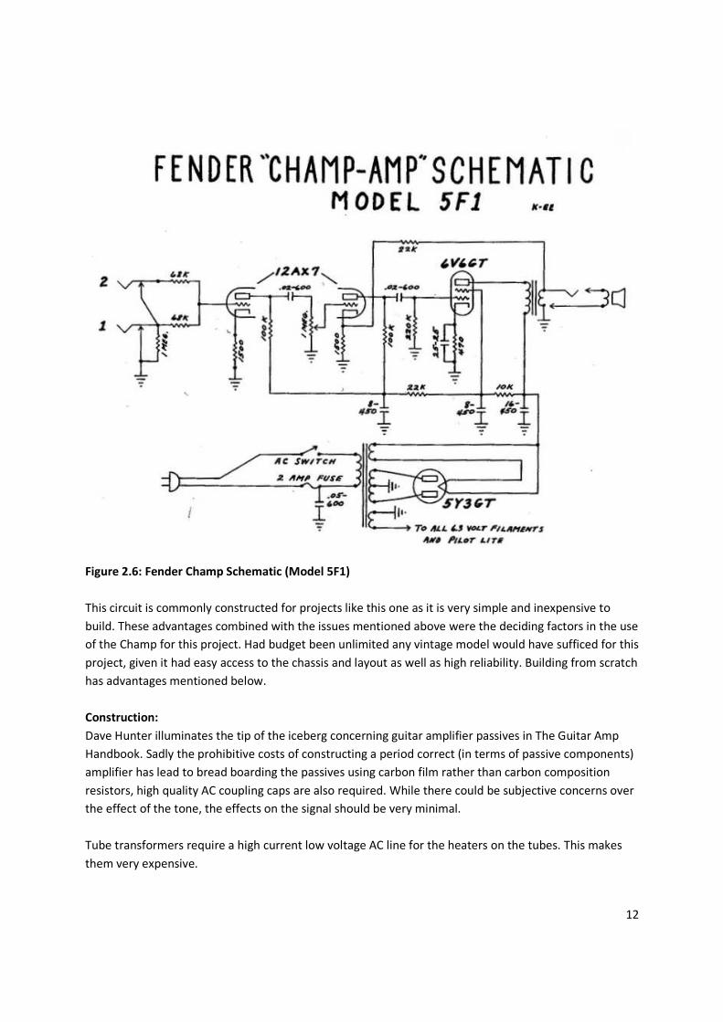
Figure 2.6: Fender Champ Schematic (Model 5F1)
This circuit is commonly constructed for projects like this one as it is very simple and inexpensive to
build. These advantages combined with the issues mentioned above were the deciding factors in the use
of the Champ for this project. Had budget been unlimited any vintage model would have sufficed for this
project, given it had easy access to the chassis and layout as well as high reliability. Building from scratch
has advantages mentioned below.
Construction:
Dave Hunter illuminates the tip of the iceberg concerning guitar amplifier passives in The Guitar Amp
Handbook. Sadly the prohibitive costs of constructing a period correct (in terms of passive components)
amplifier has lead to bread boarding the passives using carbon film rather than carbon composition
resistors, high quality AC coupling caps are also required. While there could be subjective concerns over
the effect of the tone, the effects on the signal should be very minimal.
Tube transformers require a high current low voltage AC line for the heaters on the tubes. This makes
them very expensive.
13
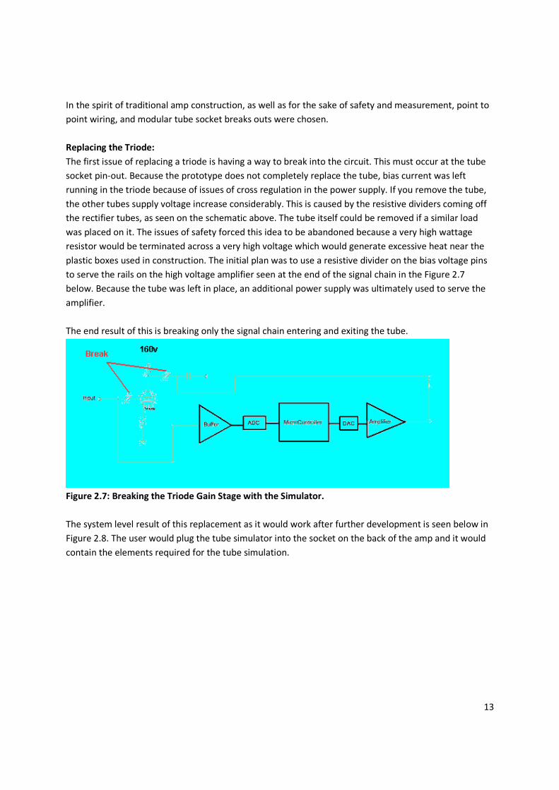
In the spirit of traditional amp construction, as well as for the sake of safety and measurement, point to
point wiring, and modular tube socket breaks outs were chosen.
Replacing the Triode:
The first issue of replacing a triode is having a way to break into the circuit. This must occur at the tube
socket pin-out. Because the prototype does not completely replace the tube, bias current was left
running in the triode because of issues of cross regulation in the power supply. If you remove the tube,
the other tubes supply voltage increase considerably. This is caused by the resistive dividers coming off
the rectifier tubes, as seen on the schematic above. The tube itself could be removed if a similar load
was placed on it. The issues of safety forced this idea to be abandoned because a very high wattage
resistor would be terminated across a very high voltage which would generate excessive heat near the
plastic boxes used in construction. The initial plan was to use a resistive divider on the bias voltage pins
to serve the rails on the high voltage amplifier seen at the end of the signal chain in the Figure 2.7
below. Because the tube was left in place, an additional power supply was ultimately used to serve the
amplifier.
The end result of this is breaking only the signal chain entering and exiting the tube.
Figure 2.7: Breaking the Triode Gain Stage with the Simulator.
The system level result of this replacement as it would work after further development is seen below in
Figure 2.8. The user would plug the tube simulator into the socket on the back of the amp and it would
contain the elements required for the tube simulation.
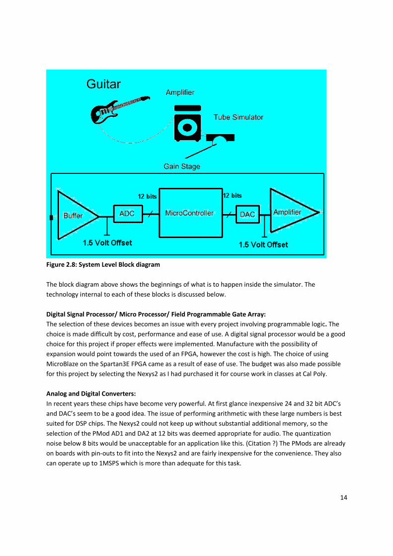
14
Figure 2.8: System Level Block diagram
The block diagram above shows the beginnings of what is to happen inside the simulator. The
technology internal to each of these blocks is discussed below.
Digital Signal Processor/ Micro Processor/ Field Programmable Gate Array:
The selection of these devices becomes an issue with every project involving programmable logic. The
choice is made difficult by cost, performance and ease of use. A digital signal processor would be a good
choice for this project if proper effects were implemented. Manufacture with the possibility of
expansion would point towards the used of an FPGA, however the cost is high. The choice of using
MicroBlaze on the Spartan3E FPGA came as a result of ease of use. The budget was also made possible
for this project by selecting the Nexys2 as I had purchased it for course work in classes at Cal Poly.
Analog and Digital Converters:
In recent years these chips have become very powerful. At first glance inexpensive 24 and 32 bit ADC’s
and DAC’s seem to be a good idea. The issue of performing arithmetic with these large numbers is best
suited for DSP chips. The Nexys2 could not keep up without substantial additional memory, so the
selection of the PMod AD1 and DA2 at 12 bits was deemed appropriate for audio. The quantization
noise below 8 bits would be unacceptable for an application like this. (Citation ?) The PMods are already
on boards with pin-outs to fit into the Nexys2 and are fairly inexpensive for the convenience. They also
can operate up to 1MSPS which is more than adequate for this task.
15
Level Shifting Low Pass Filters:
Depending on implementation methods, low pass filters are a must at the input and output of digital
systems that handle signals. The possibility of future applications using fast Fourier transforms must be
band limited to avoid aliasing and imaging on the input and output of the system. In this case a single
supply op amp is also necessary for level shifting the ADC and DAC which are single supply, more on this
is presented later in the requirements section. AC coupling with very large high quality capacitors
eliminates the necessary DC offset. This is important for operation very similar to the vacuum tube itself.
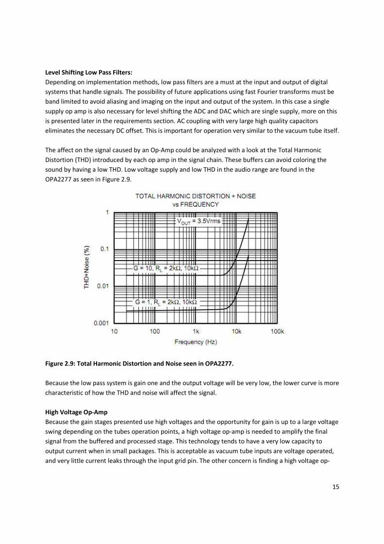
The affect on the signal caused by an Op-Amp could be analyzed with a look at the Total Harmonic
Distortion (THD) introduced by each op amp in the signal chain. These buffers can avoid coloring the
sound by having a low THD. Low voltage supply and low THD in the audio range are found in the
OPA2277 as seen in Figure 2.9.
Figure 2.9: Total Harmonic Distortion and Noise seen in OPA2277.
Because the low pass system is gain one and the output voltage will be very low, the lower curve is more
characteristic of how the THD and noise will affect the signal.
High Voltage Op-Amp
Because the gain stages presented use high voltages and the opportunity for gain is up to a large voltage
swing depending on the tubes operation points, a high voltage op-amp is needed to amplify the final
signal from the buffered and processed stage. This technology tends to have a very low capacity to
output current when in small packages. This is acceptable as vacuum tube inputs are voltage operated,
and very little current leaks through the input grid pin. The other concern is finding a high voltage op-
16
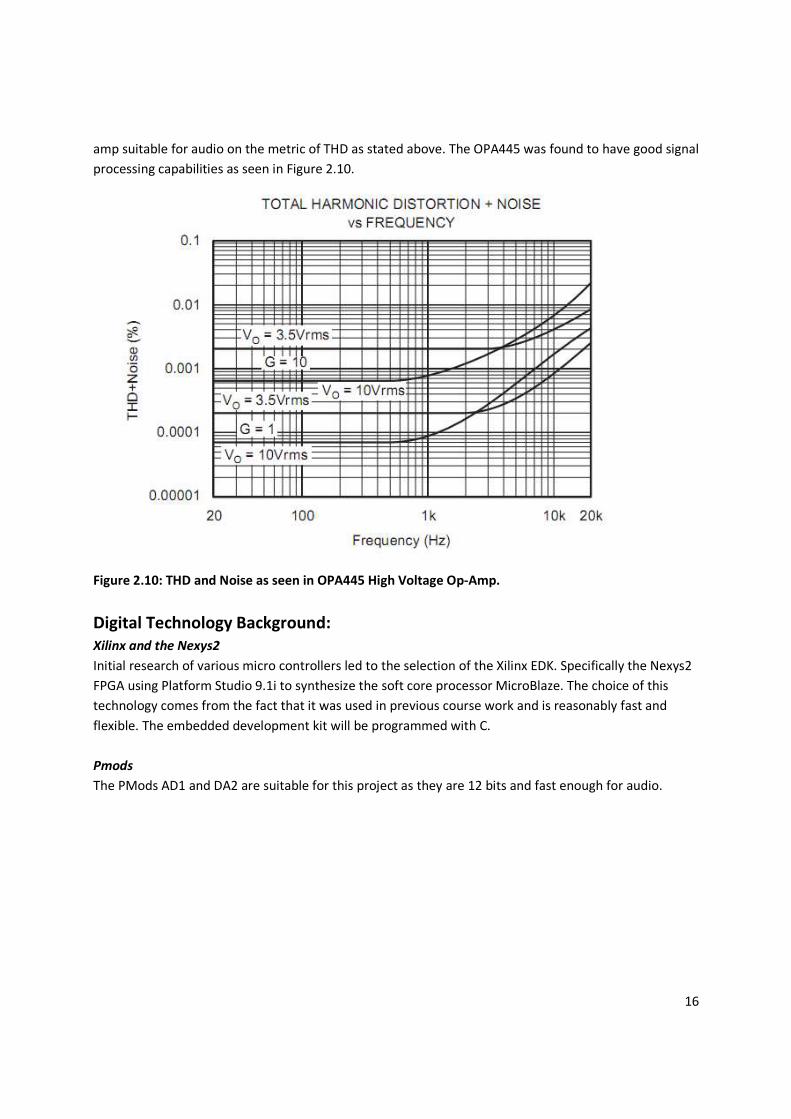
amp suitable for audio on the metric of THD as stated above. The OPA445 was found to have good signal
processing capabilities as seen in Figure 2.10.
Figure 2.10: THD and Noise as seen in OPA445 High Voltage Op-Amp.
Digital Technology Background:
Xilinx and the Nexys2
Initial research of various micro controllers led to the selection of the Xilinx EDK. Specifically the Nexys2
FPGA using Platform Studio 9.1i to synthesize the soft core processor MicroBlaze. The choice of this
technology comes from the fact that it was used in previous course work and is reasonably fast and
flexible. The embedded development kit will be programmed with C.
Pmods
The PMods AD1 and DA2 are suitable for this project as they are 12 bits and fast enough for audio.
17
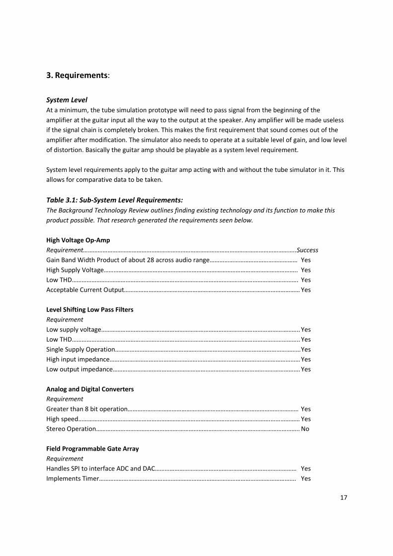
3. Requirements:
System Level
At a minimum, the tube simulation prototype will need to pass signal from the beginning of the
amplifier at the guitar input all the way to the output at the speaker. Any amplifier will be made useless
if the signal chain is completely broken. This makes the first requirement that sound comes out of the
amplifier after modification. The simulator also needs to operate at a suitable level of gain, and low level
of distortion. Basically the guitar amp should be playable as a system level requirement.
System level requirements apply to the guitar amp acting with and without the tube simulator in it. This
allows for comparative data to be taken.
Table 3.1: Sub-System Level Requirements:
The Background Technology Review outlines finding existing technology and its function to make this
product possible. That research generated the requirements seen below.
High Voltage Op-Amp
Requirement…………………………………………………………………………………………………………………..Success
Gain Band Width Product of about 28 across audio range……………………………………………… Yes
High Supply Voltage……………………………………………………………………………………………………….. Yes
Low THD…………………………………………………………………………………………………………………………. Yes
Acceptable Current Output……………………………………………………………………………………………… Yes
Level Shifting Low Pass Filters
Requirement
Low supply voltage………………………………………………………………………………………………………….. Yes
Low THD………………………………………………………………………………………………………………………….. Yes
Single Supply Operation…………………………………………………………………………………………………… Yes
High input impedance……………………………………………………………………………………………………… Yes
Low output impedance……………………………………………………………………………………………………. Yes
Analog and Digital Converters
Requirement
Greater than 8 bit operation…………………………………………………………………………………………… Yes
High speed……………………………………………………………………………………………………….……………… Yes
Stereo Operation…………………………………………………………………………………………………………….. No
Field Programmable Gate Array
Requirement
Handles SPI to interface ADC and DAC…………………………………………………………………………… Yes
Implements Timer…………………………………………………………………………………………………………. Yes

18
Adequate Memory………………………………………………………………………………………………………… No
Mathematic Handling of Data……………………………………………………………………………………….. No
Software
Requirement
Recieves signal from ADC………………………………………………………………………………………………… Yes
Sends signal to DAC…………………………………………………………………………………….…………………… Yes
Implements Transfer Function…………………………………………………………………………………………. No
19
4. Design:
This section focuses mainly on the circuit design process for the analog section, and the intellectual
property in the digital section. Some consideration to layout was taken during the design phase,
however the integration and test results section features the final assembly and layout of the complete
system.
Analog:
System Level
Because the Champ has been designed for over 50 years, no design work is required for the
circuit. The layout however requires great care to avoid noise. The power supply is isolated fairly
well in one box, and the tubes are set in breakouts for safety. More on this in the integration
section.
Sub System Level
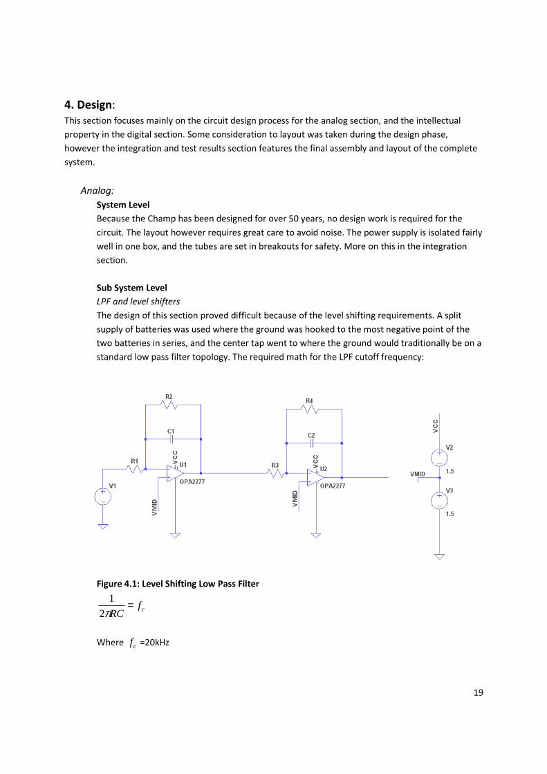
LPF and level shifters
The design of this section proved difficult because of the level shifting requirements. A split
supply of batteries was used where the ground was hooked to the most negative point of the
two batteries in series, and the center tap went to where the ground would traditionally be on a
standard low pass filter topology. The required math for the LPF cutoff frequency:
Figure 4.1: Level Shifting Low Pass Filter
cfRC
=π2
1
Where cf =20kHz
20
Values Selected:
R = 68kOhm
C=100pF
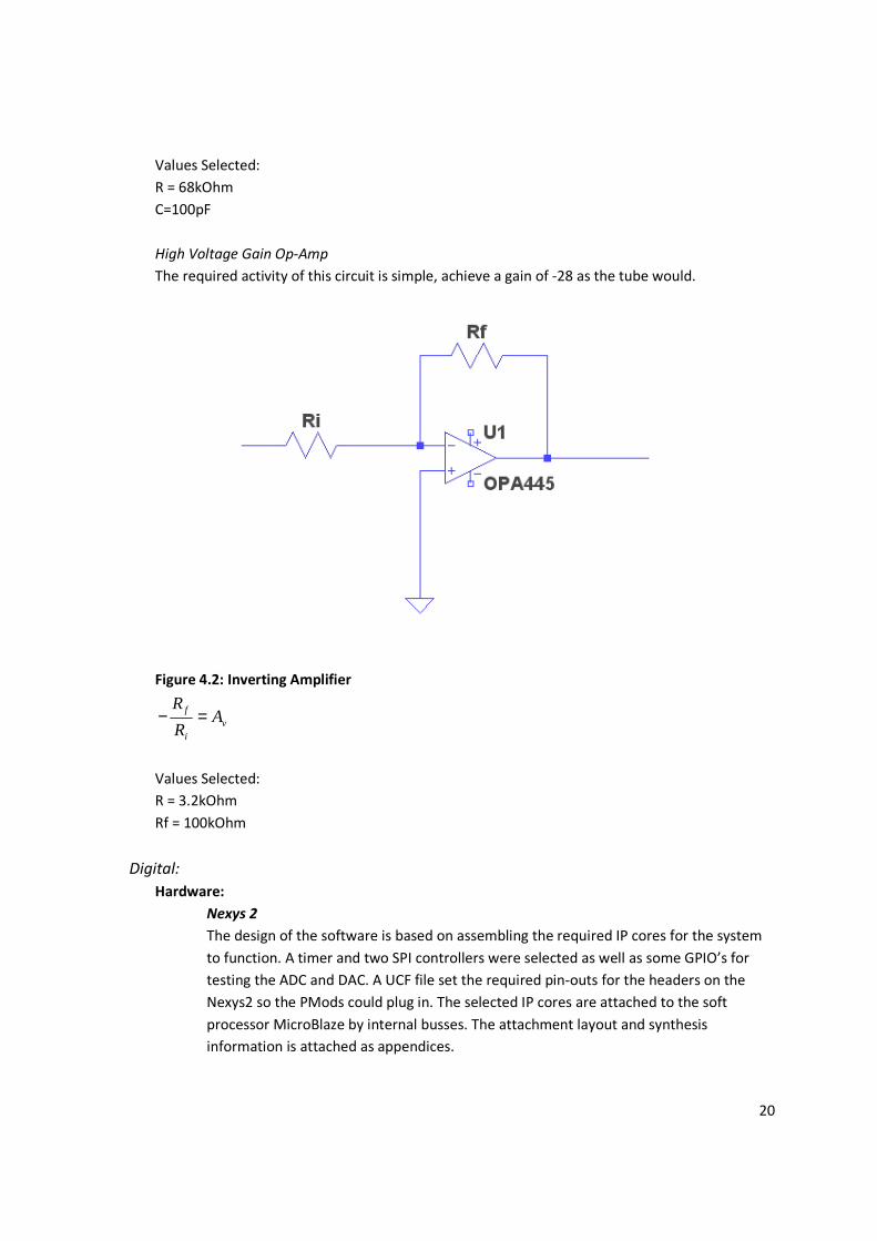
High Voltage Gain Op-Amp
The required activity of this circuit is simple, achieve a gain of -28 as the tube would.
Figure 4.2: Inverting Amplifier
vi
f AR
R=−
Values Selected:
R = 3.2kOhm
Rf = 100kOhm
Digital:
Hardware:
Nexys 2
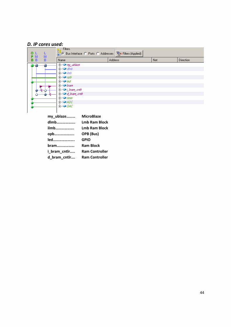
The design of the software is based on assembling the required IP cores for the system
to function. A timer and two SPI controllers were selected as well as some GPIO’s for
testing the ADC and DAC. A UCF file set the required pin-outs for the headers on the
Nexys2 so the PMods could plug in. The selected IP cores are attached to the soft
processor MicroBlaze by internal busses. The attachment layout and synthesis
information is attached as appendices.
21
AD1
This chip works with SPI interface and is powered with the Nexys2 pinout. The design
required for this is sharing a ground to the rest of the amp and receiving the signal from
the low pass buffer.
DA2
This chip also works with SPI interface and is powered with the Nexys2 pinout. The
design required for this is sharing a ground to the rest of the amp and sending the signal
to the low pass buffer.
Software:
The software is organized into functions. The GPIO’s send to the LED’s for the sake of
troubleshooting. Function calls for the SPI send bit masked hex values to control registers that
are sent according to the timing diagrams. Since two SPI IP cores are used each device can
function as its own master. This is an advantage of using MicroBlaze. The code used is attached
in an appendix.
While several attempts to generate proper code for this project were made, time constraints
stopped the ability of expansion on the Nexys2. There was simply not enough memory to
contain the massive tables of I/0 data for the transfer function, nor was the device capable of
doing the mathematics for tube simulation in real time. Every issue standard to digital signal
processing halted the ability of the Nexys2 to handle warping the signal in the same way the
vacuum tube would.
Had time allowed the Pmod for breaking in an SD card would be installed with adequate
memory. Various methods are available to retrieve data that are fast enough to be transparent
in the audio signal. The initial concept here was to make a table of input and output values
where the input could be used as the index of an array holding the appropriate output value.
This would achieve time domain warping of the signal.
22
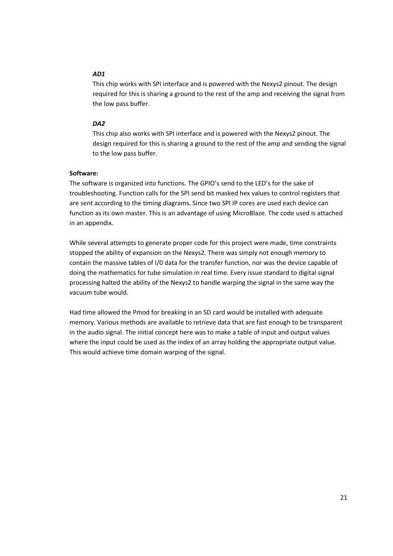
Figure 4.3: Scaled Transfer Function of Tube as Digital points in 12 bits.
23
5. Test Plans:
System Level:
Turn the amplifier on and play guitar through. If the system sounds similar with and without the tube
simulator installed this test is successful. The objective requirement would be any sound at all coming
out. Testing similarity between the signals is subjective on the system level. Below the more scientific
comparison of each stage is done on the sub system level in the integration and test results section.
Sub System Level
This section discusses how to inspect each element of the simulator for proper operation.
Level shifter circuits
The level shifter circuits are required to set the input guitar signal to 1.5 volts DC. The ADC and
DAC inputs and outputs have a single positive supply. This means the incoming wave forms must
be centered between zero and three volts for the transfer function to work properly. A further
band limiting second order low pass filter is set in case an fft is used to avoid aliasing and imaging
on either side of the digital logic. These are then AC coupled to avoid the DC value’s effect on the
rest of the amplifier.
To test:
Check Level Shifting
With board powered by the two C batteries check DC voltage at input and output of OPA2277. To
pass the value with no signal is 1.5v
Check Low Pass Filter Operation
With board powered, AC couple input and output with large capacitors. Input sinusoidal wave
form. Inspect AC coupled output as frequency is increased on the function generator. The cut off
frequency is achieved when the output is .707*(Vin). To pass this value should be near or above
20kHz.
High Voltage Op-Amp
This device should output a gain of about thirty in the audio band.
To test:
Check Gain
Apply 12 volts to the rails V+ and V-. Input sinusoid at 0.4 volts. Inspect output wave form barely
touching rails. Adjust frequency and check for change in output. 3dB cutoff should be well above
20kHz
24
Testing Nexys2
This board is programmed using the bit file generated by the Xilinx EDK. A computer loads the Nexys2
using the Digilent adept software. The green light indicates it is on and the yellow light brightens when
the device is programmed. If the device is working properly audio will be coming out of the speakers. To
ensure audio is running through this circuit simply turn it off while signal is passing through.
Testing DAC
Any number of tests for proper operation of the DAC could be devised for this depending on what other
sub systems are working first. I tested by outputting DC values and checked them with a meter to test if
this was working. The hex values to send via SPI range from 0 to 4095. This then corresponds to about 0
to 3volts. So dac_send(4096 >> 1) will output 1.5VDC.
Testing ADC
Once the SPI code is working this can be tested using the LED’s. I used a sonar distance sensor to the
input of the ADC. The signal input was coded to output to the LED’s after bit shifting to fit the max data
to LED 7. Any analog signal could be used for this test.
25
6. Development and Construction
This section puts faces to the names above. Discussion of construction and assembly issues are followed
by photos of each subsystem and part required to get the project functional.
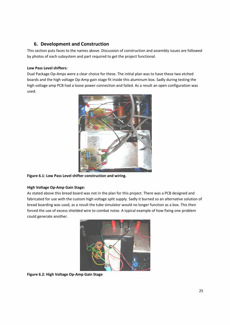
Low Pass Level shifters:
Dual Package Op-Amps were a clear choice for these. The initial plan was to have these two etched
boards and the high voltage Op-Amp gain stage fit inside this aluminum box. Sadly during testing the
high voltage amp PCB had a loose power connection and failed. As a result an open configuration was
used.
Figure 6.1: Low Pass Level shifter construction and wiring.
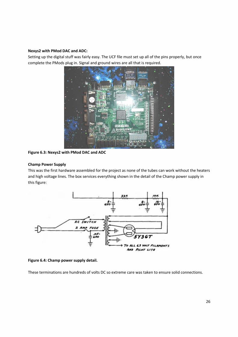
High Voltage Op-Amp Gain Stage:
As stated above this bread board was not in the plan for this project. There was a PCB designed and
fabricated for use with the custom high voltage split supply. Sadly it burned so an alternative solution of
bread boarding was used, as a result the tube simulator would no longer function as a box. This then
forced the use of excess shielded wire to combat noise. A typical example of how fixing one problem
could generate another.
Figure 6.2: High Voltage Op-Amp Gain Stage
26
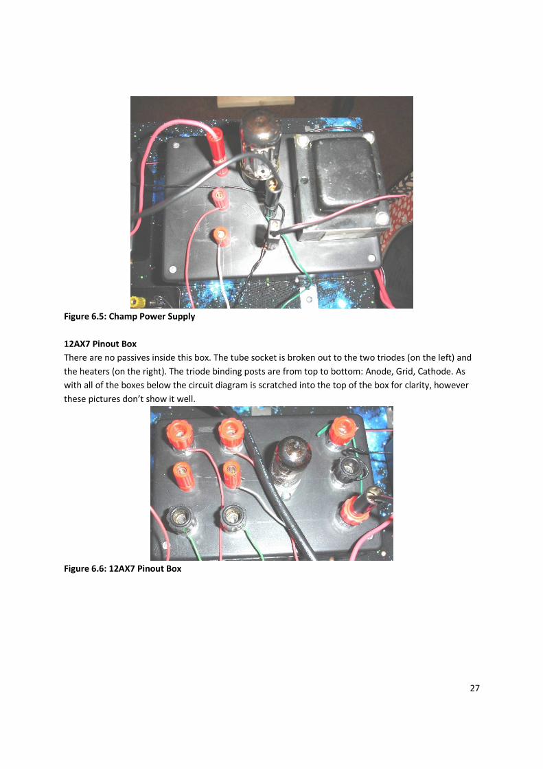
Nexys2 with PMod DAC and ADC:
Setting up the digital stuff was fairly easy. The UCF file must set up all of the pins properly, but once
complete the PMods plug in. Signal and ground wires are all that is required.
Figure 6.3: Nexys2 with PMod DAC and ADC
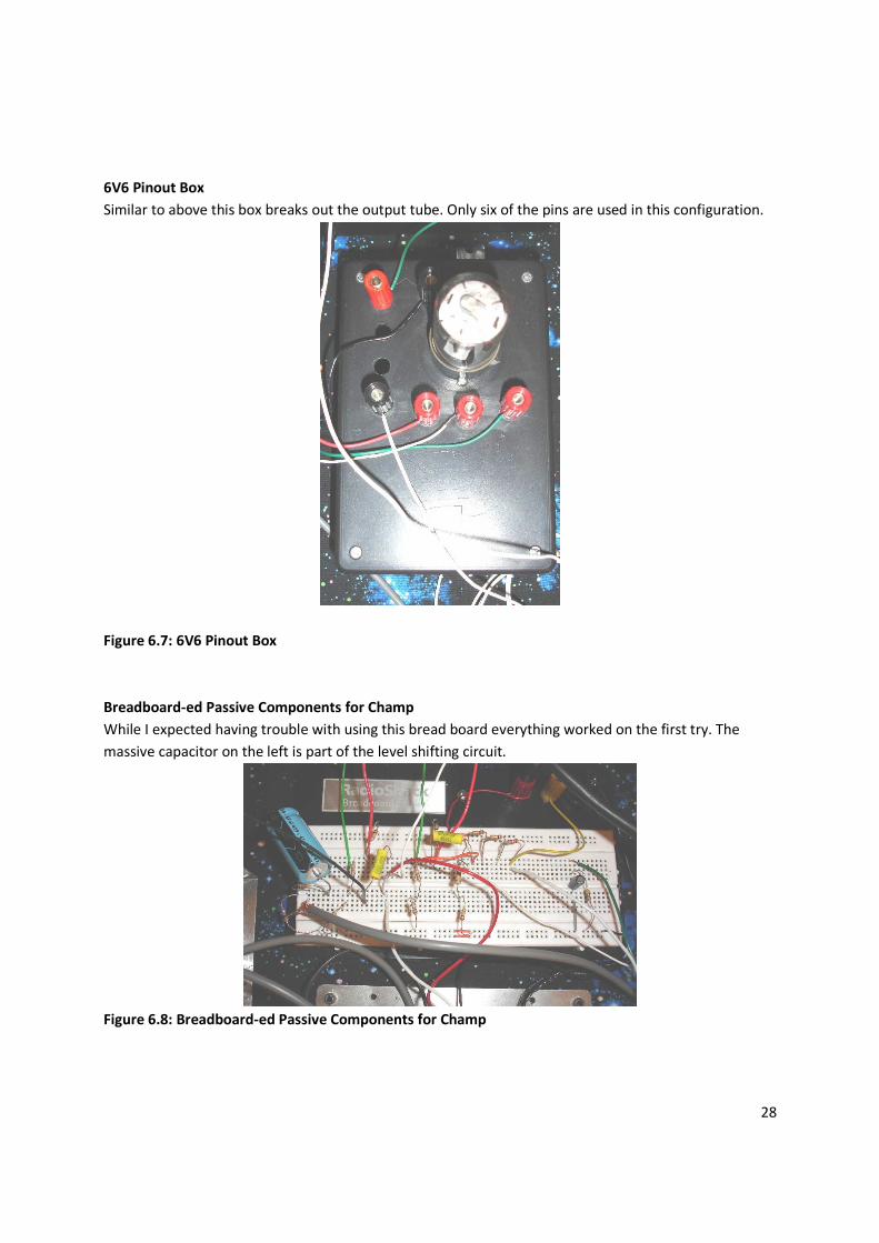
Champ Power Supply
This was the first hardware assembled for the project as none of the tubes can work without the heaters
and high voltage lines. The box services everything shown in the detail of the Champ power supply in
this figure:
Figure 6.4: Champ power supply detail.
These terminations are hundreds of volts DC so extreme care was taken to ensure solid connections.
27
Figure 6.5: Champ Power Supply
12AX7 Pinout Box
There are no passives inside this box. The tube socket is broken out to the two triodes (on the left) and
the heaters (on the right). The triode binding posts are from top to bottom: Anode, Grid, Cathode. As
with all of the boxes below the circuit diagram is scratched into the top of the box for clarity, however
these pictures don’t show it well.
Figure 6.6: 12AX7 Pinout Box
28
6V6 Pinout Box
Similar to above this box breaks out the output tube. Only six of the pins are used in this configuration.
Figure 6.7: 6V6 Pinout Box
Breadboard-ed Passive Components for Champ
While I expected having trouble with using this bread board everything worked on the first try. The
massive capacitor on the left is part of the level shifting circuit.
Figure 6.8: Breadboard-ed Passive Components for Champ
29
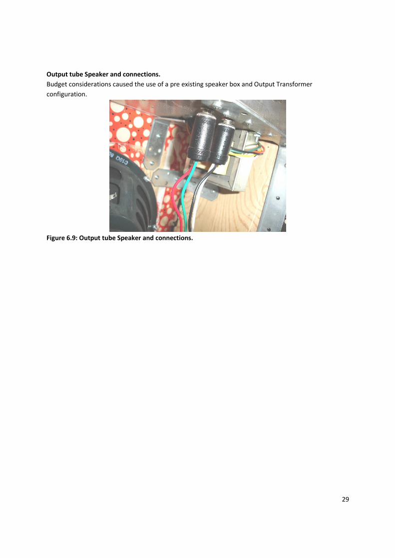
Output tube Speaker and connections.
Budget considerations caused the use of a pre existing speaker box and Output Transformer
configuration.
Figure 6.9: Output tube Speaker and connections.
30
7. Test Results and Integration:
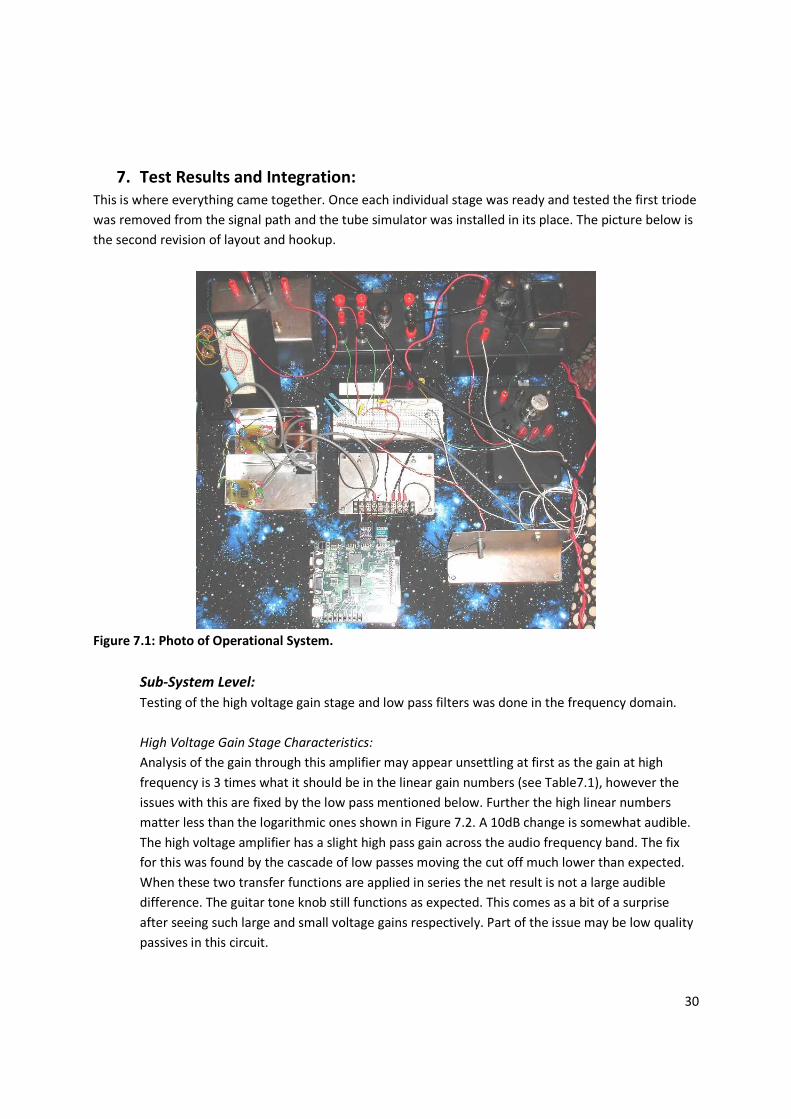
This is where everything came together. Once each individual stage was ready and tested the first triode
was removed from the signal path and the tube simulator was installed in its place. The picture below is
the second revision of layout and hookup.
Figure 7.1: Photo of Operational System.
Sub-System Level:
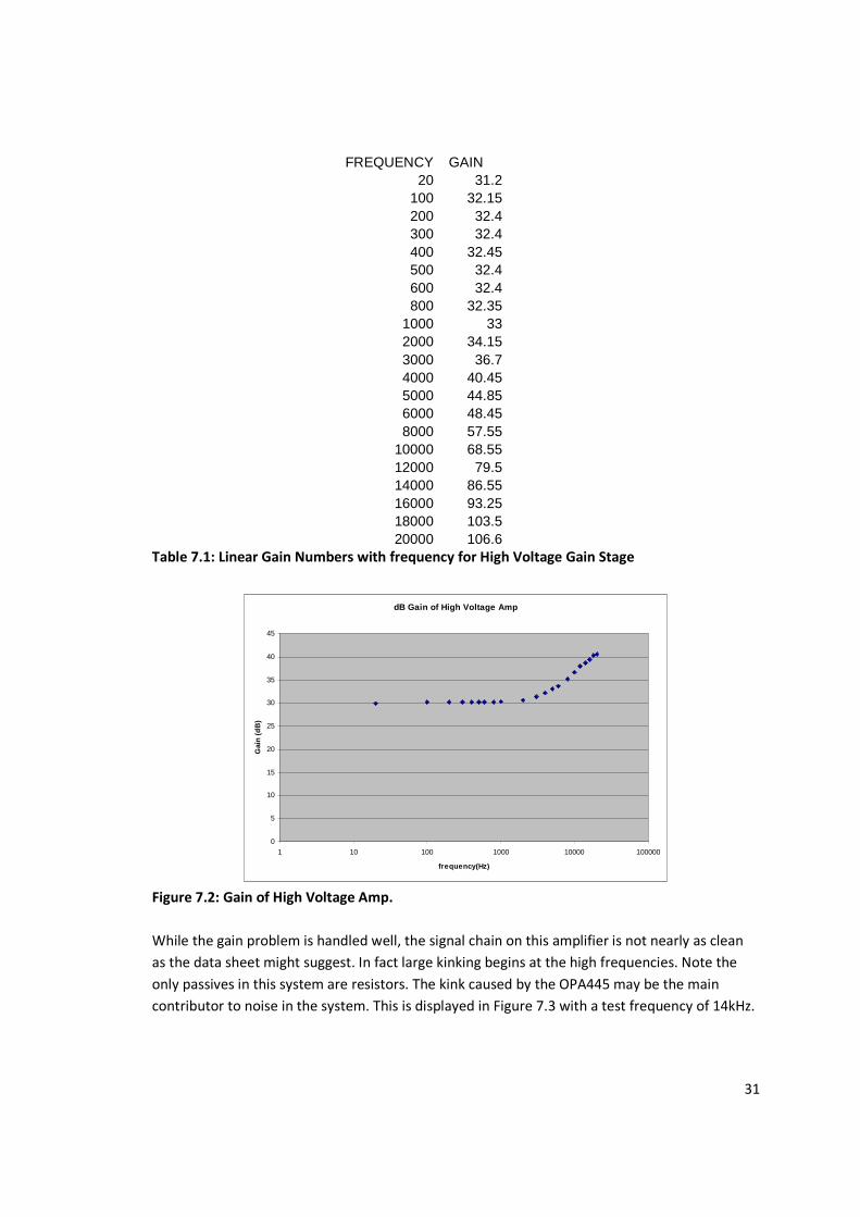
Testing of the high voltage gain stage and low pass filters was done in the frequency domain.
High Voltage Gain Stage Characteristics:
Analysis of the gain through this amplifier may appear unsettling at first as the gain at high
frequency is 3 times what it should be in the linear gain numbers (see Table7.1), however the
issues with this are fixed by the low pass mentioned below. Further the high linear numbers
matter less than the logarithmic ones shown in Figure 7.2. A 10dB change is somewhat audible.
The high voltage amplifier has a slight high pass gain across the audio frequency band. The fix
for this was found by the cascade of low passes moving the cut off much lower than expected.
When these two transfer functions are applied in series the net result is not a large audible
difference. The guitar tone knob still functions as expected. This comes as a bit of a surprise
after seeing such large and small voltage gains respectively. Part of the issue may be low quality
passives in this circuit.
31
FREQUENCY GAIN 20 31.2
100 32.15 200 32.4 300 32.4 400 32.45 500 32.4 600 32.4 800 32.35
1000 33 2000 34.15 3000 36.7 4000 40.45 5000 44.85 6000 48.45 8000 57.55
10000 68.55 12000 79.5 14000 86.55 16000 93.25 18000 103.5 20000 106.6
Table 7.1: Linear Gain Numbers with frequency for High Voltage Gain Stage
dB Gain of High Voltage Amp
0
5
10
15
20
25
30
35
40
45
1 10 100 1000 10000 100000
frequency(Hz)
Gai
n (
dB
)
Figure 7.2: Gain of High Voltage Amp.
While the gain problem is handled well, the signal chain on this amplifier is not nearly as clean
as the data sheet might suggest. In fact large kinking begins at the high frequencies. Note the
only passives in this system are resistors. The kink caused by the OPA445 may be the main
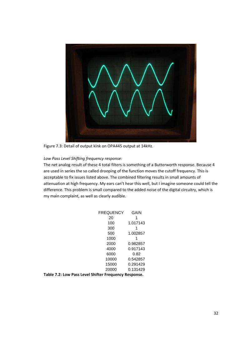
contributor to noise in the system. This is displayed in Figure 7.3 with a test frequency of 14kHz.
32
Figure 7.3: Detail of output kink on OPA445 output at 14kHz.
Low Pass Level Shifting frequency response:
The net analog result of these 4 total filters is something of a Butterworth response. Because 4
are used in series the so called drooping of the function moves the cutoff frequency. This is
acceptable to fix issues listed above. The combined filtering results in small amounts of
attenuation at high frequency. My ears can’t hear this well, but I imagine someone could tell the
difference. This problem is small compared to the added noise of the digital circuitry, which is
my main complaint, as well as clearly audible.
FREQUENCY GAIN 20 1 100 1.017143 300 1 500 1.002857
1000 1 2000 0.982857 4000 0.917143 6000 0.82 10000 0.542857 15000 0.291429 20000 0.131429
Table 7.2: Low Pass Level Shifter Frequency Response.
33
Analog Activity of Low Pass Level Shifter
-20
-18
-16
-14
-12
-10
-8
-6
-4
-2
0
2
1 10 100 1000 10000 100000
frequency(Hz)
Gai
n(d
B)
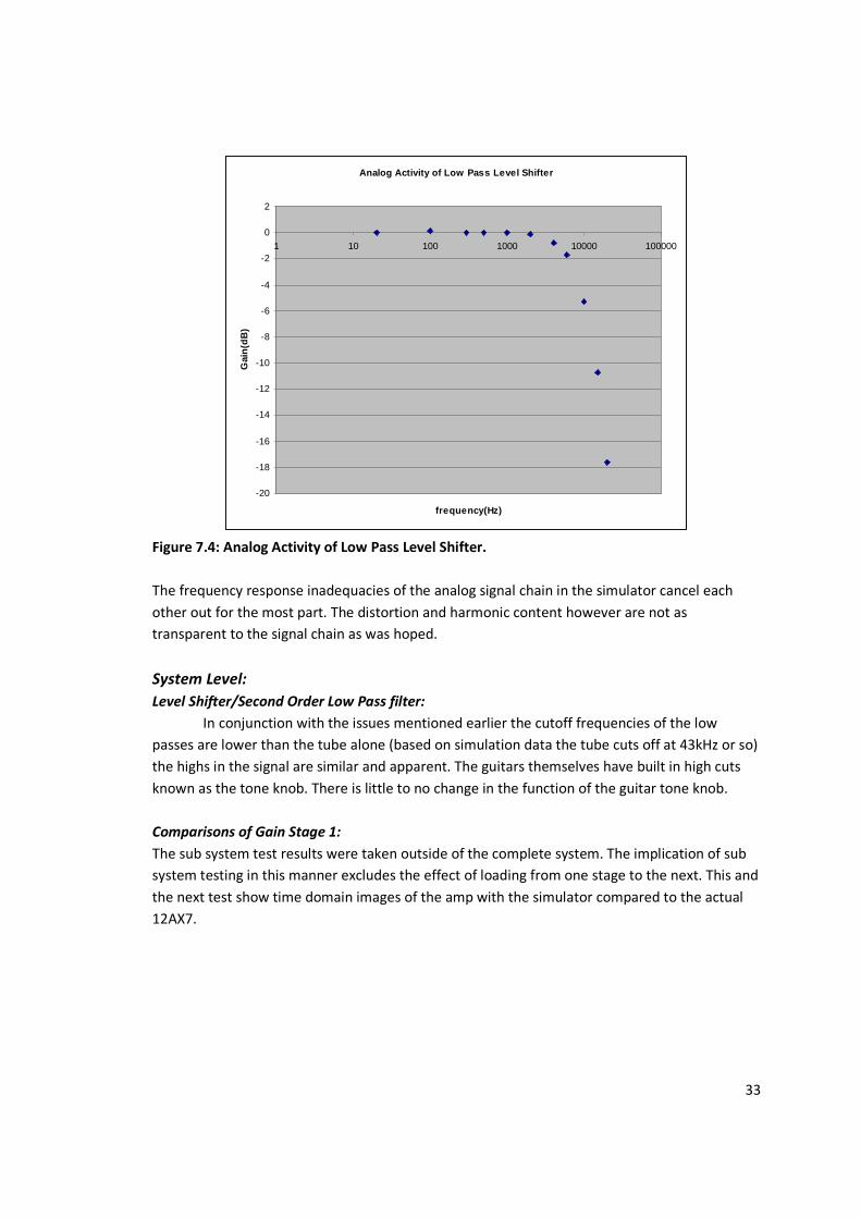
Figure 7.4: Analog Activity of Low Pass Level Shifter.
The frequency response inadequacies of the analog signal chain in the simulator cancel each
other out for the most part. The distortion and harmonic content however are not as
transparent to the signal chain as was hoped.
System Level:
Level Shifter/Second Order Low Pass filter:
In conjunction with the issues mentioned earlier the cutoff frequencies of the low
passes are lower than the tube alone (based on simulation data the tube cuts off at 43kHz or so)
the highs in the signal are similar and apparent. The guitars themselves have built in high cuts
known as the tone knob. There is little to no change in the function of the guitar tone knob.
Comparisons of Gain Stage 1:
The sub system test results were taken outside of the complete system. The implication of sub
system testing in this manner excludes the effect of loading from one stage to the next. This and
the next test show time domain images of the amp with the simulator compared to the actual
12AX7.
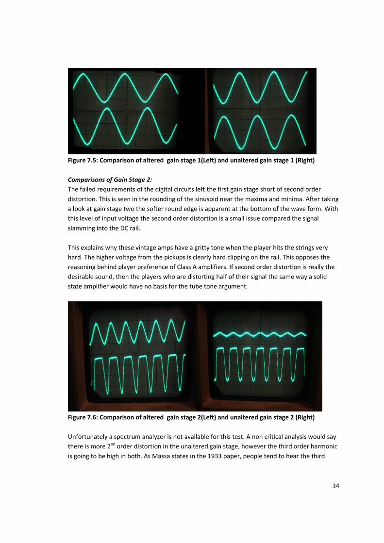
34
Figure 7.5: Comparison of altered gain stage 1(Left) and unaltered gain stage 1 (Right)
Comparisons of Gain Stage 2:
The failed requirements of the digital circuits left the first gain stage short of second order
distortion. This is seen in the rounding of the sinusoid near the maxima and minima. After taking
a look at gain stage two the softer round edge is apparent at the bottom of the wave form. With
this level of input voltage the second order distortion is a small issue compared the signal
slamming into the DC rail.
This explains why these vintage amps have a gritty tone when the player hits the strings very
hard. The higher voltage from the pickups is clearly hard clipping on the rail. This opposes the
reasoning behind player preference of Class A amplifiers. If second order distortion is really the
desirable sound, then the players who are distorting half of their signal the same way a solid
state amplifier would have no basis for the tube tone argument.
Figure 7.6: Comparison of altered gain stage 2(Left) and unaltered gain stage 2 (Right)
Unfortunately a spectrum analyzer is not available for this test. A non critical analysis would say
there is more 2nd order distortion in the unaltered gain stage, however the third order harmonic
is going to be high in both. As Massa states in the 1933 paper, people tend to hear the third
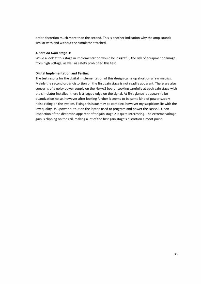
35
order distortion much more than the second. This is another indication why the amp sounds
similar with and without the simulator attached.
A note on Gain Stage 3:
While a look at this stage in implementation would be insightful, the risk of equipment damage
from high voltage, as well as safety prohibited this test.
Digital Implementation and Testing:
The test results for the digital implementation of this design came up short on a few metrics.
Mainly the second order distortion on the first gain stage is not readily apparent. There are also
concerns of a noisy power supply on the Nexys2 board. Looking carefully at each gain stage with
the simulator installed, there is a jagged edge on the signal. At first glance it appears to be
quantization noise, however after looking further it seems to be some kind of power supply
noise riding on the system. Fixing this issue may be complex, however my suspicions lie with the
low quality USB power output on the laptop used to program and power the Nexys2. Upon
inspection of the distortion apparent after gain stage 2 is quite interesting. The extreme voltage
gain is clipping on the rail, making a lot of the first gain stage’s distortion a moot point.
36
Conclusion:
High quality components and high speed digital equipment can be reasonably transparent in the audio
signal chain. This project has demonstrated considerable success in this dimension. Human ears are
somewhat insensitive to issues that appear significant on paper. The subjective tests that don’t
generate a similar response to the amp operating normally are the pop noise from plugging the cable
into the guitar and the noise caused by the digital circuits, which with some effort could probably be
eliminated.
The tone of the amplifier is seemingly preserved during normal play. Testing of gain stage 2 showed how
at high volumes the hard clipping may make the second order distortion of the tube less paramount to
the final sound. Another considerable amount of distortion is generated by the 6V6 output tube. Further
research on the power tube would be required to make a definitive statement on its effects.
The tube stigma is warranted in terms of claims of distortion and soft clipping, however the anti solid
state attitude associated with the tubes by guitarists is not totally necessary. Hard clipping has been
there for many great recordings. This being said the same musician may want to record their amplifier
with the most precise microphone on the market. This is a confusing prospect, as the sound on the
recording was processed through a historically constructed imperfect microphone. Let alone the miles of
Reel to Reel tape involved and post processing.
Future research on distortion and the attitude of the music equipment industry are endless. This project
has taken a good look at inserting modern technology into one of the oldest amplifiers in common use
today. With a little more work and a keen eye for the preservation of audio processing technology, the
vintage sounds of the past can remain with us despite the worlds changing manufacturing base and
need for sustainability.
37
Bibliography:
Blencowe, Merlin. Designing Tube Preamps for Guitar and Bass. N.p.: Merlin Blencowe, 2009. 1-
36. Print.
Hood, John Linsley. Valve and Transistor Audio Amplifiers. Oxford: Elsevier, 1997. Print.
Hunter, Dave. The Guitar Amp Handbook. San Francisco: Backbeat Books, 2005. Print.
Mass, Frank: Proceedings of the institute of radio engineers Volume 21, Number 5 May 1933
General Electric, Tube Department. “12AX7 Twin Triode Description and Rating”. June, 1953
General Electric, Tube Department. “6V6-GT-5V6-GT Beam Pentode”. March, 1955
RCA, Tube Department. “5Y3-Full Wave Vacuum Rectifier”. Jan, 1, 1951
Digilent. “Digilent Nexys2 Board Reference Manual”. June 21, 2008
Digilent. “Digilent PmodDA2 Digital To Analog Module Converter Board Reference Manual”.
September 25, 2006
Digilent. “Digilent PmodAD1 Digital To Analog Module Converter Board Reference Manual”.
April 12, 2005
38
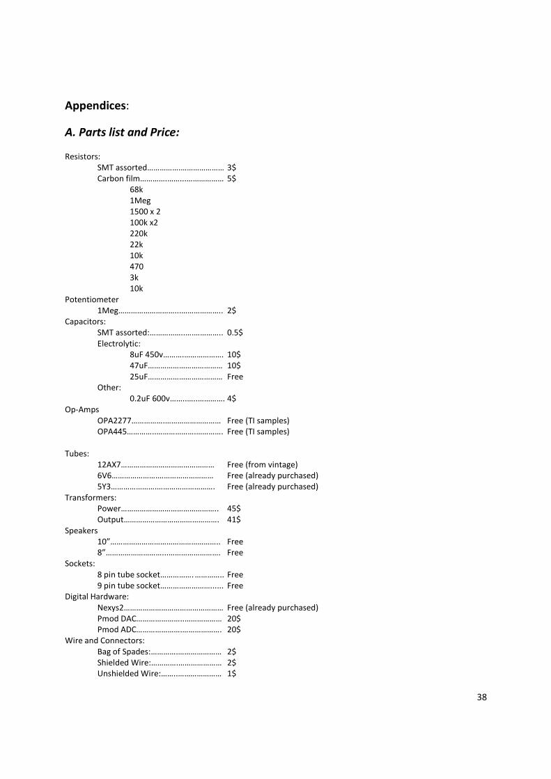
Appendices:
A. Parts list and Price:
Resistors:
SMT assorted…………….………………… 3$
Carbon film………….……...……………… 5$
68k
1Meg
1500 x 2
100k x2
220k
22k
10k
470
3k
10k
Potentiometer
1Meg………………………...……………….. 2$
Capacitors:
SMT assorted:……………..….………….. 0.5$
Electrolytic:
8uF 450v……….………………. 10$
47uF……………………………… 10$
25uF……………………………… Free
Other:
0.2uF 600v……..…..…………. 4$
Op-Amps
OPA2277…………….……………………… Free (TI samples)
OPA445…………..……………….…………. Free (TI samples)
Tubes:
12AX7……………………………………… Free (from vintage)
6V6………………….……………………… Free (already purchased)
5Y3………………….………………………. Free (already purchased)
Transformers:
Power……………………………………….. 45$
Output………………………………………. 41$
Speakers
10”…………………………………………….. Free
8”………………………...……………………. Free
Sockets:
8 pin tube socket……………. ………….. Free
9 pin tube socket……………………...... Free
Digital Hardware:
Nexys2………………………………………… Free (already purchased)
Pmod DAC…………………..……………… 20$
Pmod ADC………………….………………. 20$
Wire and Connectors:
Bag of Spades:………….………………… 2$
Shielded Wire:………….………………… 2$
Unshielded Wire:……..………………… 1$
39
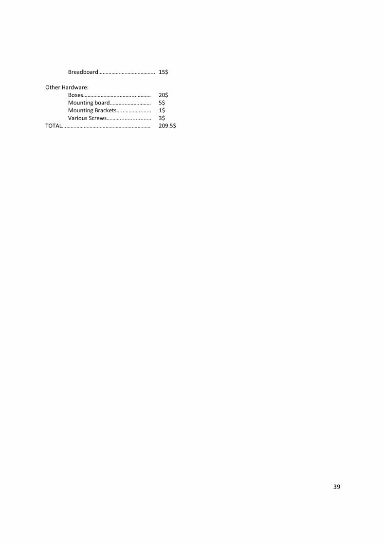
Breadboard…………….………………….. 15$
Other Hardware:
Boxes……………………..……....………. 20$
Mounting board………....…………… 5$
Mounting Brackets…..….……........ 1$
Various Screws……….................... 3$
TOTAL………………………………………….………… 209.5$
40
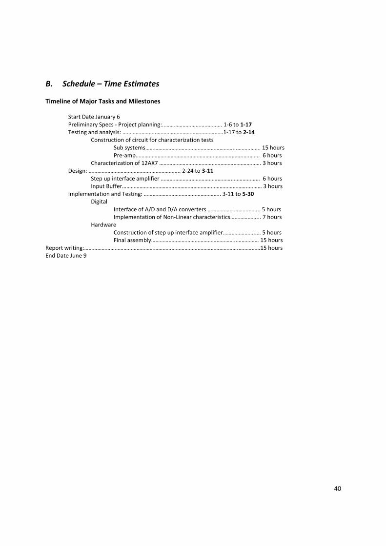
B. Schedule – Time Estimates
Timeline of Major Tasks and Milestones
Start Date January 6
Preliminary Specs - Project planning:..………………………..………. 1-6 to 1-17
Testing and analysis: …………………..…………………………….…………1-17 to 2-14
Construction of circuit for characterization tests
Sub systems……………………………………………………...……………. 15 hours
Pre-amp………………………………………………………………..….……. 6 hours
Characterization of 12AX7 ……………………………………………………………. 3 hours
Design: ………………………………….………………….. 2-24 to 3-11
Step up interface amplifier …………………………………………..……………… 6 hours
Input Buffer……………………………….…………………………………………..……… 3 hours
Implementation and Testing: …………………………………………….. 3-11 to 5-30
Digital
Interface of A/D and D/A converters ……………………….…….. 5 hours
Implementation of Non-Linear characteristics………………... 7 hours
Hardware
Construction of step up interface amplifier…………………..… 5 hours
Final assembly…………………………………………………..…………… 15 hours
Report writing:…………………………………………………………………………………………….……………15 hours
End Date June 9
41
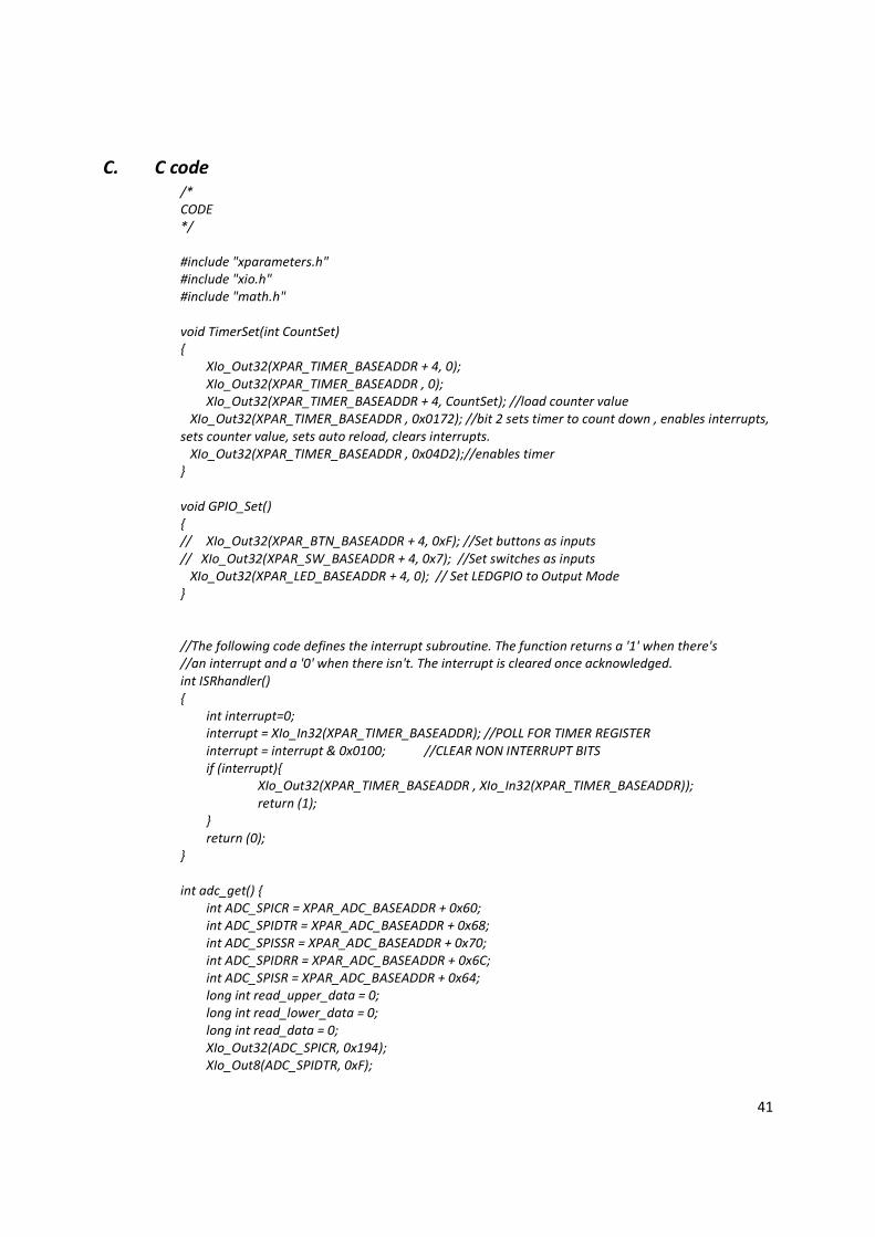
C. C code
/*
CODE
*/
#include "xparameters.h"
#include "xio.h"
#include "math.h"
void TimerSet(int CountSet)
{
XIo_Out32(XPAR_TIMER_BASEADDR + 4, 0);
XIo_Out32(XPAR_TIMER_BASEADDR , 0);
XIo_Out32(XPAR_TIMER_BASEADDR + 4, CountSet); //load counter value
XIo_Out32(XPAR_TIMER_BASEADDR , 0x0172); //bit 2 sets timer to count down , enables interrupts,
sets counter value, sets auto reload, clears interrupts.
XIo_Out32(XPAR_TIMER_BASEADDR , 0x04D2);//enables timer
}
void GPIO_Set()
{
// XIo_Out32(XPAR_BTN_BASEADDR + 4, 0xF); //Set buttons as inputs
// XIo_Out32(XPAR_SW_BASEADDR + 4, 0x7); //Set switches as inputs
XIo_Out32(XPAR_LED_BASEADDR + 4, 0); // Set LEDGPIO to Output Mode
}
//The following code defines the interrupt subroutine. The function returns a '1' when there's
//an interrupt and a '0' when there isn't. The interrupt is cleared once acknowledged.
int ISRhandler()
{
int interrupt=0;
interrupt = XIo_In32(XPAR_TIMER_BASEADDR); //POLL FOR TIMER REGISTER
interrupt = interrupt & 0x0100; //CLEAR NON INTERRUPT BITS
if (interrupt){
XIo_Out32(XPAR_TIMER_BASEADDR , XIo_In32(XPAR_TIMER_BASEADDR));
return (1);
}
return (0);
}
int adc_get() {
int ADC_SPICR = XPAR_ADC_BASEADDR + 0x60;
int ADC_SPIDTR = XPAR_ADC_BASEADDR + 0x68;
int ADC_SPISSR = XPAR_ADC_BASEADDR + 0x70;
int ADC_SPIDRR = XPAR_ADC_BASEADDR + 0x6C;
int ADC_SPISR = XPAR_ADC_BASEADDR + 0x64;
long int read_upper_data = 0;
long int read_lower_data = 0;
long int read_data = 0;
XIo_Out32(ADC_SPICR, 0x194);
XIo_Out8(ADC_SPIDTR, 0xF);
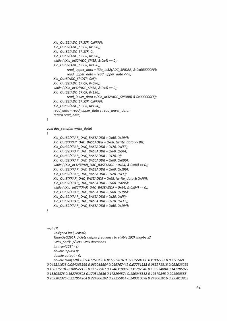
42
XIo_Out32(ADC_SPISSR, 0xFFFF);
XIo_Out32(ADC_SPICR, 0x096);
XIo_Out32(ADC_SPISSR, 0);
XIo_Out32(ADC_SPICR, 0x096);
while ( (XIo_In32(ADC_SPISR) & 0x4) == 0);
XIo_Out32(ADC_SPICR, 0x196);
read_upper_data = (XIo_In32(ADC_SPIDRR) & 0x000000FF);
read_upper_data = read_upper_data << 8;
XIo_Out8(ADC_SPIDTR, 0xF);
XIo_Out32(ADC_SPICR, 0x096);
while ( (XIo_In32(ADC_SPISR) & 0x4) == 0);
XIo_Out32(ADC_SPICR, 0x196);
read_lower_data = (XIo_In32(ADC_SPIDRR) & 0x000000FF);
XIo_Out32(ADC_SPISSR, 0xFFFF);
XIo_Out32(ADC_SPICR, 0x194);
read_data = read_upper_data | read_lower_data;
return read_data;
}
void dac_send(int write_data)
{
XIo_Out32(XPAR_DAC_BASEADDR + 0x60, 0x194);
XIo_Out8(XPAR_DAC_BASEADDR + 0x68, (write_data >> 8));
XIo_Out32(XPAR_DAC_BASEADDR + 0x70, 0xFFF);
XIo_Out32(XPAR_DAC_BASEADDR + 0x60, 0x96);
XIo_Out32(XPAR_DAC_BASEADDR + 0x70, 0);
XIo_Out32(XPAR_DAC_BASEADDR + 0x60, 0x096);
while ( (XIo_In32(XPAR_DAC_BASEADDR + 0x64) & 0x04) == 0);
XIo_Out32(XPAR_DAC_BASEADDR + 0x60, 0x196);
XIo_Out32(XPAR_DAC_BASEADDR + 0x20, 0xFF);
XIo_Out8(XPAR_DAC_BASEADDR + 0x68, (write_data & 0xFF));
XIo_Out32(XPAR_DAC_BASEADDR + 0x60, 0x096);
while ( (XIo_In32(XPAR_DAC_BASEADDR + 0x64) & 0x04) == 0);
XIo_Out32(XPAR_DAC_BASEADDR + 0x60, 0x196);
XIo_Out32(XPAR_DAC_BASEADDR + 0x20, 0xFF);
XIo_Out32(XPAR_DAC_BASEADDR + 0x70, 0xFFF);
XIo_Out32(XPAR_DAC_BASEADDR + 0x60, 0x194);
}
main(){
unsigned int i, leds=0;
TimerSet(261); //Sets output frequency to visible 192k maybe x2
GPIO_Set(); //Sets GPIO directions
int tran[128] = {}
double input = 0;
double output = 0;
double tran[128] = {0.007751938 0.015503876 0.023255814 0.031007752 0.03875969
0.046511628 0.054263566 0.062015504 0.069767442 0.07751938 0.085271318 0.093023256
0.100775194 0.108527132 0.11627907 0.124031008 0.131782946 0.139534884 0.147286822
0.15503876 0.162790698 0.170542636 0.178294574 0.186046512 0.19379845 0.201550388
0.209302326 0.217054264 0.224806202 0.23255814 0.240310078 0.248062016 0.255813953
43
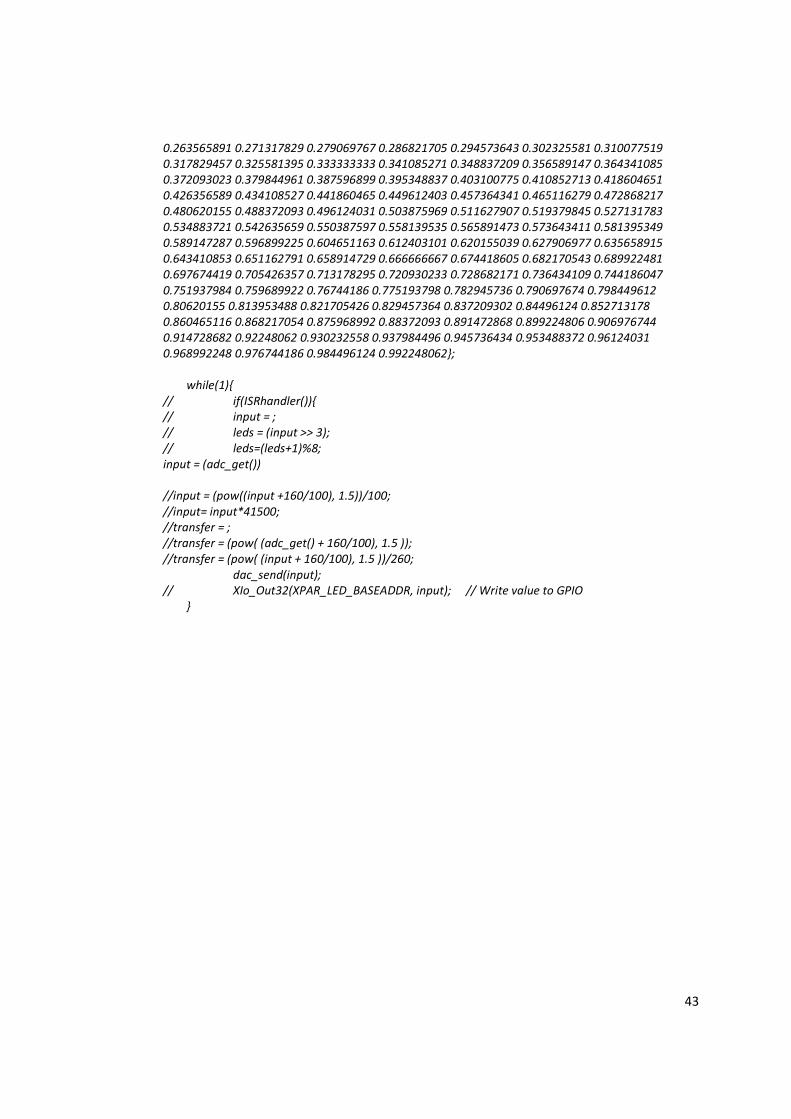
0.263565891 0.271317829 0.279069767 0.286821705 0.294573643 0.302325581 0.310077519
0.317829457 0.325581395 0.333333333 0.341085271 0.348837209 0.356589147 0.364341085
0.372093023 0.379844961 0.387596899 0.395348837 0.403100775 0.410852713 0.418604651
0.426356589 0.434108527 0.441860465 0.449612403 0.457364341 0.465116279 0.472868217
0.480620155 0.488372093 0.496124031 0.503875969 0.511627907 0.519379845 0.527131783
0.534883721 0.542635659 0.550387597 0.558139535 0.565891473 0.573643411 0.581395349
0.589147287 0.596899225 0.604651163 0.612403101 0.620155039 0.627906977 0.635658915
0.643410853 0.651162791 0.658914729 0.666666667 0.674418605 0.682170543 0.689922481
0.697674419 0.705426357 0.713178295 0.720930233 0.728682171 0.736434109 0.744186047
0.751937984 0.759689922 0.76744186 0.775193798 0.782945736 0.790697674 0.798449612
0.80620155 0.813953488 0.821705426 0.829457364 0.837209302 0.84496124 0.852713178
0.860465116 0.868217054 0.875968992 0.88372093 0.891472868 0.899224806 0.906976744
0.914728682 0.92248062 0.930232558 0.937984496 0.945736434 0.953488372 0.96124031
0.968992248 0.976744186 0.984496124 0.992248062};
while(1){
// if(ISRhandler()){
// input = ;
// leds = (input >> 3);
// leds=(leds+1)%8;
input = (adc_get())
//input = (pow((input +160/100), 1.5))/100;
//input= input*41500;
//transfer = ;
//transfer = (pow( (adc_get() + 160/100), 1.5 ));
//transfer = (pow( (input + 160/100), 1.5 ))/260;
dac_send(input);
// XIo_Out32(XPAR_LED_BASEADDR, input); // Write value to GPIO
}
44
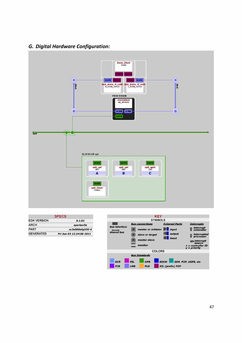
D. IP cores used:
my_ublaze……… MicroBlaze
dlmb………………. Lmb Ram Block
ilmb………………. Lmb Ram Block
opb……………….. OPB (Bus)
led…………………. GPIO
bram……………… Ram Block
i_bram_cntlr….. Ram Controller
d_bram_cntlr…. Ram Controller
45
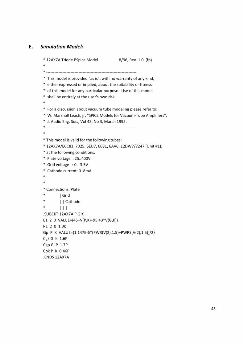
E. Simulation Model:
* 12AX7A Triode PSpice Model 8/96, Rev. 1.0 (fp)
*
* -------------------------------------------------------------------
* This model is provided "as is", with no warranty of any kind,
* either expressed or implied, about the suitability or fitness
* of this model for any particular purpose. Use of this model
* shall be entirely at the user's own risk.
*
* For a discussion about vacuum tube modeling please refer to:
* W. Marshall Leach, jr: "SPICE Models for Vacuum-Tube Amplifiers";
* J. Audio Eng. Soc., Vol 43, No 3, March 1995.
* -------------------------------------------------------------------
*
* This model is valid for the following tubes:
* 12AX7A/ECC83, 7025, 6EU7, 6681, 6AV6, 12DW7/7247 (Unit #1);
* at the following conditions:
* Plate voltage : 25..400V
* Grid voltage : 0..-3.5V
* Cathode current: 0..8mA
*
*
* Connections: Plate
* | Grid
* | | Cathode
* | | |
.SUBCKT 12AX7A P G K
E1 2 0 VALUE={45+V(P,K)+95.43*V(G,K)}
R1 2 0 1.0K
Gp P K VALUE={1.147E-6*(PWR(V(2),1.5)+PWRS(V(2),1.5))/2}
Cgk G K 1.6P
Cgp G P 1.7P
Cpk P K 0.46P
.ENDS 12AX7A
46
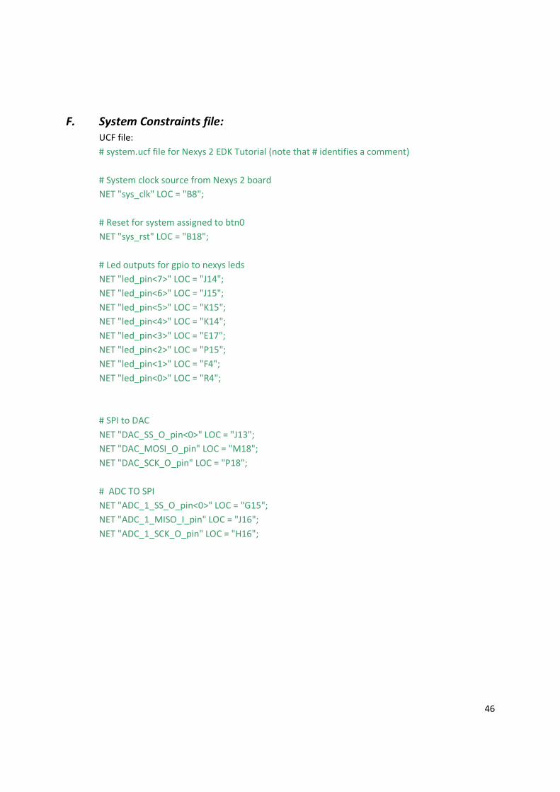
F. System Constraints file:
UCF file:
# system.ucf file for Nexys 2 EDK Tutorial (note that # identifies a comment)
# System clock source from Nexys 2 board
NET "sys_clk" LOC = "B8";
# Reset for system assigned to btn0
NET "sys_rst" LOC = "B18";
# Led outputs for gpio to nexys leds
NET "led_pin<7>" LOC = "J14";
NET "led_pin<6>" LOC = "J15";
NET "led_pin<5>" LOC = "K15";
NET "led_pin<4>" LOC = "K14";
NET "led_pin<3>" LOC = "E17";
NET "led_pin<2>" LOC = "P15";
NET "led_pin<1>" LOC = "F4";
NET "led_pin<0>" LOC = "R4";
# SPI to DAC
NET "DAC_SS_O_pin<0>" LOC = "J13";
NET "DAC_MOSI_O_pin" LOC = "M18";
NET "DAC_SCK_O_pin" LOC = "P18";
# ADC TO SPI
NET "ADC_1_SS_O_pin<0>" LOC = "G15";
NET "ADC_1_MISO_I_pin" LOC = "J16";
NET "ADC_1_SCK_O_pin" LOC = "H16";
47
G. Digital Hardware Configuration:
48
H. ANALYSIS OF SENIOR PROJECT DESIGN
Project Title: Programmable Solid State 12AX7 Triode Gain Stage Student’s Name: Ian Campbell Signature:________________________ Date:_______________ Advisor’s Name: Dr Wayne Pilkington Initials:___________________________ Date:_______________ Summary of Functional Requirements: The programmable Solid State 12AX7 Triode Gain Stage is the first steps in creating a system to replace vacuum tubes using equipment that does not wear out. It also allows for the addition of digital logic in the signal chain of vintage equipment. It gives additional options for operation of vintage equipment for audio enthusiasts. Primary Constraints: This project hit a glass ceiling with digital constraints. Initial concepts used very high quality cutting edge analog and digital converters, but it was soon found that interfacing and implementing them was too heavy on system resources for the (soft) micro controller used. Some of these issues could be attributed of budget. Because the project was so physically large, and difficult to transport, use of equipment at home forced the development of two power supplies. Developing these power supplies took away from time that could have been spent on expanding the digital features of the tube simulator. The testing was also done with an old analog scope. The effect of a physically large project being a constraint taking away from the testing options provided through equipment in the school labs. The last issue was noise. The open layout of the entire project forced shielding on the low signal wires. Many hours were spent reworking things to try to eliminate noise entering the system. Economic: The original estimated cost of the project was about 300 dollars. The project came in within the budget, due to my parts collection and free TI samples. Most of the money was spent on case work Pmods and a transformer. The additional and somewhat unexpected costs of development would be the high voltage power supply, as well as some etching equipment who’s cost is somewhat negligible. The initial development time estimates were way off. The initial plans would have required 15+ hours a week. This may have been possible on a part time course work schedule. Being that the first quarter was scheduled as all research, and I began construction at that time the time estimates are a bit off. I believe the total time across one quarter would be 6 to 8 hours a week. This is much more realistic. If manufactured on a commercial basis: The number of items sold per year for this device would probably be low. While a lot of vintage equipment still operates in the United States, 12AX7 tubes cost about 10 to 20 dollars and last for many hours of operation. The amount of time a tube simulator would have to be used to pay itself off would be very high. This being said there is always people interested in new technology and modifications of their
49
musical equipment. The manufacture would probably be viable less than 5000 annually at a sale price of about 200 dollars a unit. Cost of manufacture would be around 75 dollars. If 1000 sales are made 125,000 would be the difference between cost of manufacture and sale price, however this number would be much lower due to operating costs, such as advertising and property rental. Subtracting start up costs from this would make about 50,000 in profits. Once purchased the user would not need to spend extra money on the device as is necessary with vacuum tubes. Environmental: Impacts on the environment would be similar to any other company employing silicone devices. The etching of boards requires the use of toxic chemicals. Assembly requires solder, though this application could be lead free. Manufacturability: The concept of manufacturing these as fake tubes could use stacked PCB’s to actually achieve the look of a vacuum tube. This would tap old style construction methods which have been pretty much abandoned since the tube era. The revival of these methods would not be very costly however. Sustainability: This device improves the sustainability of using vacuum tube amplifiers. Assuming development could be done to replace all tubes in an amp with simulators of this nature, new tubes would not be needed. This lowers the disposing of glass, steel, copper, and inert gasses. Improvements to this prototype could use the pre existing power available from the amplifiers transformer and lower the use of copper and iron in tube simulator. Ethical: The best thing about working with music equipment is that it doesn’t have much in the way of negative ethical repercussions. If the product is manufactured properly, it will be safer than the original vacuum tube. The worst thing that could happen is someone could use it to make unethical music. Health and Safety: This is a big issue as all guitar amp vacuum tubes operate with transformers that run above 300 volts. Care must be taken in development not to electrocute employees or interns. Once in the market place the need for reliability is high so as to not expose the public to these high lethal voltages. This being said, there is little added danger from changing a glass tube containing high voltages to one presumably encased in epoxy. The issue of shatter would be avoided. Social and Political: The social acceptance of using solid state devices to play guitar through is low. The only hope of a project like this is to fool the purists and bring forward new options for making music. Development: The most useful tool I learned in this project was the ‘pop’ test. Testing the voltage at various stages in the amplifier causes a pop at the output. When a stage is broken the pop will not be apparent. This allows for quick detection of faults during testing and assembly. Also etching PCB’s became a big part of this project using the toner transfer method at home. Reliability of breadboards during transportation seems much lower than a properly assembled PCB.