Embed Size (px)
Citation preview
Document Number: MD00541Revision 02.14March 30, 2011
MIPS Technologies, Inc.955 East Arques Avenue
Sunnyvale, CA 94085-4521
Copyright © 2007, 2008, 2010, 2011 MIPS Technologies Inc. All rights reserved.
MIPSVerified
™
Programming the MIPS32® 74K™ CoreFamily
Programming the MIPS32® 74K™ Core Family, Revision 02.14
Copyright © 2007, 2008, 2010, 2011 MIPS Technologies Inc. All rights reserved.
Template: nB1.02, Built with tags: 2B
Copyright © 2007, 2008, 2010, 2011 MIPS Technologies, Inc. All rights reserved.
Unpublished rights (if any) reserved under the copyright laws of the United States of America and other countries.
This document contains information that is proprietary to MIPS Technologies, Inc. ("MIPS Technologies"). Any copying, reproducing, modifying or use of thisinformation (in whole or in part) that is not expressly permitted in writing by MIPS Technologies or an authorized third party is strictly prohibited. At aminimum, this information is protected under unfair competition and copyright laws. Violations thereof may result in criminal penalties and fines.
Any document provided in source format (i.e., in a modifiable form such as in FrameMaker or Microsoft Word format) is subject to use and distributionrestrictions that are independent of and supplemental to any and all confidentiality restrictions. UNDER NO CIRCUMSTANCES MAY A DOCUMENTPROVIDED IN SOURCE FORMAT BE DISTRIBUTED TO A THIRD PARTY IN SOURCE FORMAT WITHOUT THE EXPRESS WRITTENPERMISSION OF MIPS TECHNOLOGIES, INC.
MIPS Technologies reserves the right to change the information contained in this document to improve function, design or otherwise. MIPS Technologies doesnot assume any liability arising out of the application or use of this information, or of any error or omission in such information. Any warranties, whetherexpress, statutory, implied or otherwise, including but not limited to the implied warranties of merchantability or fitness for a particular purpose, are excluded.Except as expressly provided in any written license agreement from MIPS Technologies or an authorized third party, the furnishing of this document does notgive recipient any license to any intellectual property rights, including any patent rights, that cover the information in this document.
The information contained in this document shall not be exported, reexported, transferred, or released, directly or indirectly, in violation of the law of anycountry or international law, regulation, treaty, Executive Order, statute, amendments or supplements thereto. Should a conflict arise regarding the export,reexport, transfer, or release of the information contained in this document, the laws of the United States of America shall be the governing law.
The information contained in this document constitutes one or more of the following: commercial computer software, commercial computer softwaredocumentation or other commercial items. If the user of this information, or any related documentation of any kind, including related technical data or manuals,is an agency, department, or other entity of the United States government ("Government"), the use, duplication, reproduction, release, modification, disclosure,or transfer of this information, or any related documentation of any kind, is restricted in accordance with Federal Acquisition Regulation 12.212 for civilianagencies and Defense Federal Acquisition Regulation Supplement 227.7202 for military agencies. The use of this information by the Government is furtherrestricted in accordance with the terms of the license agreement(s) and/or applicable contract terms and conditions covering this information from MIPSTechnologies or an authorized third party.
MIPS, MIPS I, MIPS II, MIPS III, MIPS IV, MIPS V, MIPSr3, MIPS32, MIPS64, microMIPS32, microMIPS64, MIPS-3D, MIPS16, MIPS16e, MIPS-Based,MIPSsim, MIPSpro, MIPS Technologies logo, MIPS-VERIFIED, MIPS-VERIFIED logo, 4K, 4Kc, 4Km, 4Kp, 4KE, 4KEc, 4KEm, 4KEp, 4KS, 4KSc, 4KSd,M4K, M14K, 5K, 5Kc, 5Kf, 24K, 24Kc, 24Kf, 24KE, 24KEc, 24KEf, 34K, 34Kc, 34Kf, 74K, 74Kc, 74Kf, 1004K, 1004Kc, 1004Kf, R3000, R4000, R5000,ASMACRO, Atlas, "At the core of the user experience.", BusBridge, Bus Navigator, CLAM, CorExtend, CoreFPGA, CoreLV, EC, FPGA View, FS2, FS2FIRST SILICON SOLUTIONS logo, FS2 NAVIGATOR, HyperDebug, HyperJTAG, IASim, JALGO, Logic Navigator, Malta, MDMX, MED, MGB,microMIPS, OCI, PDtrace, the Pipeline, Pro Series, SEAD, SEAD-2, SmartMIPS, SOC-it, System Navigator, and YAMON are trademarks or registeredtrademarks of MIPS Technologies, Inc. in the United States and other countries.
All other trademarks referred to herein are the property of their respective owners.
3 Programming the MIPS32® 74K™ Core Family, Revision 02.14
Copyright © 2007, 2008, 2010, 2011 MIPS Technologies Inc. All rights reserved.
Table of Contents
Chapter 1: Introduction ........................................................................................................................ 111.1: Chapters of this manual............................................................................................................................. 121.2: Conventions............................................................................................................................................... 121.3: 74K™ core features................................................................................................................................... 131.4: A brief guide to the 74K™ core implementation ........................................................................................ 14
1.4.1: Notes on pipeline overview diagram (Figure 1.1):............................................................................ 141.4.2: Branches and branch delays............................................................................................................ 171.4.3: Loads and load-to-use delays .......................................................................................................... 181.4.4: Queues, Resource limits and Consequences .................................................................................. 19
Chapter 2: Initialization and identity ................................................................................................... 212.1: Probing your CPU - Config CP0 registers ................................................................................................. 21
2.1.1: The Config register........................................................................................................................... 222.1.2: The Config1-2 registers.................................................................................................................... 232.1.3: The Config3 register......................................................................................................................... 242.1.4: The Config6 register......................................................................................................................... 252.1.5: CPU-specific configuration — Config7............................................................................................. 26
2.2: PRId register — identifying your CPU type ............................................................................................... 26
Chapter 3: Memory map, caching, reads, writes and translation .................................................... 293.1: The memory map ...................................................................................................................................... 293.2: Fixed mapping option ................................................................................................................................ 303.3: Reads, writes and synchronization............................................................................................................ 30
3.3.1: Read/write ordering and cache/memory data queues in the 74K™ core ......................................... 303.3.2: The “sync” instruction in 74K™ family cores .................................................................................... 313.3.3: Write gathering and “write buffer flushing” in 74K™ family cores..................................................... 32
3.4: Caches ...................................................................................................................................................... 323.4.1: The L2 cache option......................................................................................................................... 323.4.2: Cacheability options ......................................................................................................................... 333.4.3: Uncached accelerated writes ........................................................................................................... 343.4.4: The cache instruction and software cache management................................................................. 343.4.5: Cache instructions and CP0 cache tag/data registers ..................................................................... 353.4.6: L1 Cache instruction timing.............................................................................................................. 373.4.7: L2 cache instruction timing............................................................................................................... 373.4.8: Cache management when writing instructions - the “synci” instruction ........................................... 373.4.9: Cache aliases................................................................................................................................... 383.4.10: Cache locking................................................................................................................................. 393.4.11: Cache initialization and tag/data registers ..................................................................................... 393.4.12: L23TagLo Regiser.......................................................................................................................... 403.4.13: L23DataLo Register ....................................................................................................................... 403.4.14: L23DataHi Register........................................................................................................................ 403.4.15: TagLo registers in special modes .................................................................................................. 413.4.16: Parity error exception handling and the CacheErr register ............................................................ 413.4.17: ErrCtl register ................................................................................................................................. 42
3.5: Bus error exception ................................................................................................................................... 433.6: Scratchpad memory/SPRAM..................................................................................................................... 443.7: Common Device Memory Map .................................................................................................................. 46
Programming the MIPS32® 74K™ Core Family, Revision 02.14 4
Copyright © 2007, 2008, 2010, 2011 MIPS Technologies Inc. All rights reserved.
3.8: The TLB and translation ............................................................................................................................ 473.8.1: A TLB entry ...................................................................................................................................... 473.8.2: Live translation and micro-TLBs....................................................................................................... 483.8.3: Reading and writing TLB entries: Index, Random and Wired .......................................................... 483.8.4: Reading and writing TLB entries - EntryLo0-1, EntryHi and PageMask registers............................ 493.8.5: TLB initialization and duplicate entries............................................................................................. 503.8.6: TLB exception handlers — BadVaddr, Context, and ContextConfig registers................................. 51
Chapter 4: Programming the 74K™ core in user mode .................................................................... 554.1: User-mode accessible “Hardware registers” ............................................................................................. 554.2: Prefetching data ........................................................................................................................................ 564.3: Using “synci” when writing instructions...................................................................................................... 564.4: The multiplier ............................................................................................................................................. 574.5: Tuning software for the 74K™ family pipeline ........................................................................................... 58
4.5.1: Cache delays and mitigating their effect .......................................................................................... 584.5.2: Branch delay slot.............................................................................................................................. 59
4.6: Tuning floating-point .................................................................................................................................. 594.7: Branch misprediction delays...................................................................................................................... 604.8: Load delayed by (unrelated) recent store.................................................................................................. 604.9: Minimum load-miss penalty ....................................................................................................................... 604.10: Data dependency delays ......................................................................................................................... 61
4.10.1: More complicated dependencies ................................................................................................... 644.11: Advice on tuning instruction sequences (particularly DSP) ..................................................................... 654.12: Multiply/divide unit and timings................................................................................................................ 65
Chapter 5: Kernel-mode (OS) programming and Release 2 of the MIPS32® Architecture............ 675.1: Hazard barrier instructions ........................................................................................................................ 675.2: MIPS32® Architecture Release 2 - enhanced interrupt system(s) ............................................................ 68
5.2.1: Traditional MIPS® interrupt signalling and priority ........................................................................... 695.2.2: VI mode - multiple entry points, interrupt signalling and priority....................................................... 705.2.3: External Interrupt Controller (EIC) mode.......................................................................................... 70
5.3: Exception Entry Points .............................................................................................................................. 715.3.1: Summary of exception entry points.................................................................................................. 72
5.4: Shadow registers....................................................................................................................................... 735.5: Saving Power ............................................................................................................................................ 755.6: The HWREna register - Control user rdhwr access .................................................................................. 75
Chapter 6: Floating point unit.............................................................................................................. 776.1: Data representation ................................................................................................................................... 776.2: Basic instruction set................................................................................................................................... 786.3: Floating point loads and stores.................................................................................................................. 796.4: Setting up the FPU and the FPU control registers .................................................................................... 79
6.4.1: IEEE options .................................................................................................................................... 796.4.2: FPU “unimplemented” exceptions (and how to avoid them) ............................................................ 796.4.3: FPU control register maps ............................................................................................................... 80
6.5: FPU pipeline and instruction timing ........................................................................................................... 826.5.1: FPU register dependency delays ..................................................................................................... 846.5.2: Delays caused by long-latency instructions looping in the M1 stage ............................................... 846.5.3: Delays on FP load and store instructions......................................................................................... 846.5.4: Delays when main pipeline waits for FPU to decide not to take an exception ................................. 846.5.5: Delays when main pipeline waits for FPU to accept an instruction.................................................. 856.5.6: Delays on mfc1/mtc1 instructions .................................................................................................... 85
5 Programming the MIPS32® 74K™ Core Family, Revision 02.14
Copyright © 2007, 2008, 2010, 2011 MIPS Technologies Inc. All rights reserved.
6.5.7: Delays caused by dependency on FPU status register fields .......................................................... 856.5.8: Slower operation in MIPS I™ compatibility mode ............................................................................ 85
Chapter 7: The MIPS32® DSP ASE ..................................................................................................... 877.1: Features provided by the MIPS® DSP ASE.............................................................................................. 877.2: The DSP ASE control register ................................................................................................................... 88
7.2.1: DSP accumulators ........................................................................................................................... 897.3: Software detection of the DSP ASE .......................................................................................................... 897.4: DSP instructions ........................................................................................................................................ 90
7.4.1: Hints in instruction names................................................................................................................ 907.4.2: Arithmetic - 64-bit ............................................................................................................................. 917.4.3: Arithmetic - saturating and/or SIMD Types ...................................................................................... 917.4.4: Bit-shifts - saturating and/or SIMD types.......................................................................................... 917.4.5: Comparison and “conditional-move” operations on SIMD types...................................................... 917.4.6: Conversions to and from SIMD types .............................................................................................. 927.4.7: Multiplication - SIMD types with result in GP register ...................................................................... 927.4.8: Multiply Q15s from paired-half and accumulate............................................................................... 937.4.9: Load with register + register address............................................................................................... 937.4.10: DSPControl register access ........................................................................................................... 937.4.11: Accumulator access instructions.................................................................................................... 947.4.12: Dot products and building blocks for complex multiplication.......................................................... 947.4.13: Other DSP ASE instructions .......................................................................................................... 95
7.5: Macros and typedefs for DSP instructions ................................................................................................ 957.6: Almost Alphabetically-ordered table of DSP ASE instructions .................................................................. 967.7: DSP ASE instruction timing ..................................................................................................................... 100
Chapter 8: 74K™ core features for debug and profiling................................................................. 1028.1: EJTAG on-chip debug unit ...................................................................................................................... 102
8.1.1: Debug communications through JTAG .......................................................................................... 1038.1.2: Debug mode................................................................................................................................... 1038.1.3: Exceptions in debug mode............................................................................................................. 1048.1.4: Single-stepping .............................................................................................................................. 1048.1.5: The “dseg” memory decode region ................................................................................................ 1048.1.6: EJTAG CP0 registers, particularly Debug...................................................................................... 1068.1.7: The DCR (debug control) memory-mapped register...................................................................... 1088.1.8: The DebugVectorAddr memory-mapped register .......................................................................... 1108.1.9: JTAG-accessible registers ............................................................................................................. 1108.1.10: Fast Debug Channel .................................................................................................................... 1128.1.11: EJTAG breakpoint registers ......................................................................................................... 1158.1.12: Understanding breakpoint conditions........................................................................................... 1178.1.13: Imprecise debug breaks............................................................................................................... 1188.1.14: PC Sampling with EJTAG ............................................................................................................ 1188.1.15: JTAG-accessible and memory-mapped PDtrace TCB Registers ................................................ 119
8.2: PDtrace™ instruction trace facility........................................................................................................... 1218.2.1: 74K core-specific fields in PDtrace™ JTAG-accessible registers.................................................. 1218.2.2: CP0 registers for the PDtrace™ logic ............................................................................................ 1238.2.3: JTAG triggers and local control through TraceIBPC/TraceDBPC.................................................. 1258.2.4: UserTraceData1 reg and UserTraceData2 reg .............................................................................. 1268.2.5: Summary of when trace happens .................................................................................................. 126
8.3: CP0 Watchpoints..................................................................................................................................... 1288.3.1: The WatchLo0-3 registers.............................................................................................................. 1288.3.2: The WatchHi0-3 registers .............................................................................................................. 128
8.4: Performance counters ............................................................................................................................. 129
Programming the MIPS32® 74K™ Core Family, Revision 02.14 6
Copyright © 2007, 2008, 2010, 2011 MIPS Technologies Inc. All rights reserved.
8.4.1: Reading the event table. ................................................................................................................ 130
Appendix A: References .................................................................................................................... 135
Appendix B: CP0 register summary and reference......................................................................... 137B.1: Miscellaneous CP0 register descriptions ................................................................................................ 140
B.1.1: Status register................................................................................................................................ 141B.1.2: The UserLocal register .................................................................................................................. 143B.1.3: Exception control: Cause and EPC registers................................................................................. 143
B.1.3.1: The Cause register............................................................................................................... 143B.1.4: The EPC register ........................................................................................................................... 145B.1.5: Count and Compare ...................................................................................................................... 145
B.2: Registers for CPU Configuration............................................................................................................. 145B.2.1: The Config7 register ...................................................................................................................... 145
B.3: Registers for Cache Diagnostics............................................................................................................. 148B.3.1: Different views of ITagLo/DTagLo ................................................................................................. 148B.3.2: Dual (virtual and physical) tags in the 74K core D-cache — DTagHi register ............................... 149B.3.3: Pre-decode information in the I-cache - the ITagHi Register......................................................... 149B.3.4: The DDataLo, IDataHi and IDataLo registers ................................................................................ 150B.3.5: The ErrorEPC register ................................................................................................................... 150
Appendix C: MIPS® Architecture quick-reference sheet(s) ........................................................... 151C.1: General purpose register numbers and names ...................................................................................... 151C.2: User-level changes with Release 2 of the MIPS32® Architecture .......................................................... 151
C.2.1: Release 2 of the MIPS32® Architecture - new instructions for user-mode ................................... 151C.2.2: Release 2 of the MIPS32® Architecture - Hardware registers from user mode............................ 152
C.3: FPU changes in Release 2 of the MIPS32® Architecture....................................................................... 153
Appendix D: Revision History ........................................................................................................... 155
7 Programming the MIPS32® 74K™ Core Family, Revision 02.14
Copyright © 2007, 2008, 2010, 2011 MIPS Technologies Inc. All rights reserved.
List of Figures
Figure 1.1: Overview of The 74K™ Pipeline........................................................................................................... 14Figure 2.1: Fields in the Config Register................................................................................................................. 22Figure 2.2: Fields in the Config1 Register............................................................................................................... 23Figure 2.3: Fields in the Config2 Register............................................................................................................... 23Figure 2.4: Config3 Register Format....................................................................................................................... 24Figure 2.5: Config6 Register Format....................................................................................................................... 25Figure 2.6: Fields in the PRId Register ................................................................................................................... 26Figure 3.1: Fields in the encoding of a cache instruction........................................................................................ 34Figure 3.2: Fields in the TagLo Registers .............................................................................................................. 39Figure 3.3: L23TagLo Register Format ................................................................................................................... 40Figure 3.4: L23DataLo Register Format.................................................................................................................. 40Figure 3.5: L23DataHi Register Format .................................................................................................................. 41Figure 3.6: Fields in the CacheErr Register ........................................................................................................... 41Figure 3.7: Fields in the ErrCtl Register .................................................................................................................. 43Figure 3.8: SPRAM (scratchpad RAM) configuration information in TagLo............................................................ 45Figure 3-9: Fields in the CDMMBase Register........................................................................................................ 46Figure 3.10: Fields in the Access Control and Status (ACSR) Register ................................................................. 47Figure 3.11: Fields in a 74K™ core TLB entry ........................................................................................................ 48Figure 3.12: Fields in the EntryHi and PageMask registers .................................................................................... 49Figure 3.13: Fields in the EntryLo0-1 registers ....................................................................................................... 50Figure 3.14: Fields in the Context register when Config3CTXTC=0 and Config3SM=0 ......................................... 51Figure 3.15: Fields in the Context register when Config3CTXTC=1 or Config3SM=1............................................ 52Figure 3.16: Fields in the ContextConfig register................................................................................................... 53Figure 5.1: Fields in the IntCtl Register................................................................................................................... 69Figure 5.2: Fields in the EBase Register................................................................................................................. 72Figure 5.3: Fields in the SRSCtl Register ............................................................................................................... 73Figure 5.4: Fields in the SRSMap Register............................................................................................................. 74Figure 5.5: Fields in the HWREna Register ............................................................................................................ 75Figure 6.1: How floating point numbers are stored in a register ............................................................................ 78Figure 6.2: Fields in the FIR register....................................................................................................................... 80Figure 6.3: Floating point control/status register and alternate views..................................................................... 81Figure 6.4: Overview of the FPU pipeline .............................................................................................................. 83Figure 7.1: Fields in the DSPControl Register ........................................................................................................ 88Figure 8.1: Fields in the EJTAG CP0 Debug register ........................................................................................... 107Figure 8.2: Exception cause bits in the debug register ......................................................................................... 108Figure 8.3: Debug register - exception-pending flags ........................................................................................... 108Figure 8.4: Fields in the memory-mapped DCR (debug control) register ............................................................. 109Figure 8.5: Fields in the memory-mapped DCR (debug control) register ............................................................. 110Figure 8.6: IFields in the JTAG-accessible Implementation register..................................................................... 110Figure 8.7: Fields in the JTAG-accessible EJTAG_CONTROL register ............................................................... 111Figure 8.8: Fast Debug Channel ........................................................................................................................... 113Figure 8.9: Fields in the FDC Access Control and Status (FDACSR) Register .................................................... 113Figure 8.10: Fields in the FDC Config (FDCFG) Register..................................................................................... 114Figure 8.11: Fields in the FDC Status (FDSTAT) Register ................................................................................... 114Figure 8.12: Fields in the FDC Receive (FDRX) Register..................................................................................... 115Figure 8.13: Fields in the FDC Transmit (FDTXn) Registers ................................................................................ 115Figure 8.14: Fields in the IBS/DBS (EJTAG breakpoint status) registers ............................................................. 116
Programming the MIPS32® 74K™ Core Family, Revision 02.14 8
Copyright © 2007, 2008, 2010, 2011 MIPS Technologies Inc. All rights reserved.
Figure 8.15: Fields in the hardware breakpoint control registers (IBCn, DBCn) ................................................... 117Figure 8.16: Fields in the TCBCONTROLE register ............................................................................................. 122Figure 8.17: Fields in the TCBCONFIG register ................................................................................................... 123Figure 8.18: Fields in the TraceControl Register .................................................................................................. 123Figure 8.19: Fields in the TraceControl2 Register ................................................................................................ 123Figure 8.20: Fields in the TraceControl3 register.................................................................................................. 123Figure 8.21: Fields in the TraceIBPC/TraceDBPC registers ................................................................................. 125Figure 8.22: Fields in the WatchLo0-3 Register.................................................................................................... 128Figure 8.23: Fields in the WatchHi0-3 Register .................................................................................................... 128Figure 8.24: Fields in the PerfCtl0-3 Register ....................................................................................................... 129Figure B.1: Fields in the Status Register............................................................................................................... 141Figure B.2: Fields in the Cause Register .............................................................................................................. 143Figure B.3: Fields in the TagLo-WST Register ..................................................................................................... 148Figure B.4: Fields in the TagLo-DAT Register ...................................................................................................... 149Figure B.5: Fields in the DTagHi Register............................................................................................................. 149Figure B.6: Fields in the ITagHi Register .............................................................................................................. 149
9 Programming the MIPS32® 74K™ Core Family, Revision 02.14
Copyright © 2007, 2008, 2010, 2011 MIPS Technologies Inc. All rights reserved.
List of Tables
Table 2.1: Roles of Config registers........................................................................................................................ 21Table 2.2: 74K™® core releases and PRId[Revision] fields ................................................................................... 26Table 3.1: Basic MIPS32® architecture memory map ............................................................................................ 29Table 3.2: Fixed memory mapping.......................................................................................................................... 30Table 3.3: Cache Code Values ............................................................................................................................... 34Table 3.4: Operations on a cache line available with the cache instruction............................................................ 36Table 3.1: Caches and their CP0 cache tag/data registers..................................................................................... 37Table 3.5: L23DataLo Register Field Description ................................................................................................... 40Table 3.6: L23DataHi Register Field Description .................................................................................................... 41Table 3.7: Recommended ContextConfig Values................................................................................................... 53Table 4.1: Hints for “pref” instructions..................................................................................................................... 57Table 4.2: Register → eager consumer delays....................................................................................................... 62Table 4.3: Producer → register delays.................................................................................................................... 63Table 5.1: All Exception entry points....................................................................................................................... 73Table 6.1: FPU (co-processor 1) control registers .................................................................................................. 80Table 6.2: Long-latency FP instructions.................................................................................................................. 84Table 7.1: Mask bits for instructions accessing the DSPControl register................................................................ 93Table 7.2: DSP instructions in alphabetical order ................................................................................................... 96Table 8.1: JTAG instructions for the EJTAG unit .................................................................................................. 103Table 8.2: EJTAG debug memory region map (“dseg”) ........................................................................................ 105Table 8.3: Fields in the JTAG-accessible EJTAG_CONTROL register ................................................................ 111Table 8.4: FDC Register Mapping......................................................................................................................... 113Table 8.5: Mapping TCB Registers in drseg ........................................................................................................ 119Table 8.6: Fields in the TCBCONTROLA register................................................................................................. 122Table 8.7: Fields in the TCBCONTROLB register................................................................................................. 122Table 8.8: Performance Counter Event Codes in the PerfCtl0-3[Event] field. ...................................................... 131Table B.1: Register index by name....................................................................................................................... 137Table B.2: CP0 registers by number ..................................................................................................................... 138Table B.3: CP0 Registers Grouped by Function................................................................................................... 140Table B.4: Encoding privilege level in Status[UM,SM] .......................................................................................... 142Table B.5: Values found in Cause[ExcCode] ........................................................................................................ 144Table B.6: Fields in the Config7 Register.............................................................................................................. 146Table C.1: Conventional names of registers with usage mnemonics ................................................................... 151Table C.2: Release 2 of the MIPS32® Architecture - new instructions................................................................. 152

Programming the MIPS32® 74K™ Core Family, Revision 02.14 10
Copyright © 2007, 2008, 2010, 2011 MIPS Technologies Inc. All rights reserved.
Chapter 1
Programming the MIPS32® 74K™ Core Family, Revision 02.14 11
Copyright © 2007, 2008, 2010, 2011 MIPS Technologies Inc. All rights reserved.
Introduction
The MIPS32® 74K™ core is the first member of a family of synthesizable CPU cores launched in 2007, and offersthe highest performance yet from a synthesizable core. It does this by issuing two instructions simultaneously (wherepossible) and by using a long pipeline to enable relatively high frequency operation. Conventional high-throughputdesigns of this type are slowed by dependencies between consecutive instructions, so 74K family cores use out-of-order execution to work around short-term dependencies and keep the pipeline full.
74K Cores offer better performance in the same process compared to MIPS Technologies’ mid-range 24K® family, atthe cost of a larger and more complex core.
Intended Audience
This document is for programmers who are already familiar with the MIPS® architecture and who can read MIPSassembler language (if that’s not you yet, you’d probably benefit from reading a generic MIPS book - see AppendixA, “References” on page 135).
More precisely, you should definitely be reading this manual if you have an OS, compiler, or low-level applicationwhich already runs on some earlier MIPS CPU, and you want to adapt it to the 74K core. So this document concen-trates on where a MIPS 74K family core behaves differently from its predecessors. That’s either:
• Behavior which is not completely specified by Release 2 of the MIPS32® architecture: these either concern priv-ileged operation, or are timing-related.
• Behavior which was standardized only in the recent Release 2 of the MIPS32 specification (and not in previous
versions). All Release 2 features are formally documented in [MIPS32]1, and [MIPS32V1] describes the mainchanges added by Release 2.
But the summary is too brief to program from, and the details are widely spread; so you’ll find a reminder of thechanges here. Changes to user-privilege instructions are found in Appendix C, “MIPS® Architecture quick-reference sheet(s)” on page 151, and changes to kernel-privilege (OS) instructions and facilities are detailed inChapter 5, “Kernel-mode (OS) programming and Release 2 of the MIPS32® Architecture” on page 67.
• Details of timing, relevant to engineers optimizing code (and that very small audience of compiler writers), foundin Section 4.5 “Tuning software for the 74K‘ family pipeline”.
This manual is distinct from the [SUM] reference manual: that is a CPU reference organized from a hardware view-point. If you need to write processor subsystem diagnostics, this manual will not be enough! If you want a very care-ful corner-cases-included delineation of exactly what an instruction does, you’ll need [MIPS32]... and so on.
For readability, some MIPS32 material is repeated here, particularly where a reference would involve a large excur-sion for the reader for a small saving for the author. Appendices mention every user-level-programming differenceany active MIPS software engineer is likely to notice when programming the 74K core.
1. References (in square brackets) are listed in Appendix A, “References” on page 135.
1.1 Chapters of this manual
Programming the MIPS32® 74K™ Core Family, Revision 02.14 12
Copyright © 2007, 2008, 2010, 2011 MIPS Technologies Inc. All rights reserved.
All 74K cores are able to run programs encoded with the MIPS16e™ instruction set extension - which makes thebinary significantly smaller, with some trade-off in performance. MIPS16e code is rarely seen - it’s almost exclu-sively produced by compilers, and in a debugger view is pretty much a subset of the regular MIPS32 instruction set -so you’ll find no further mention of it in this manual; please refer to [MIPS16e].
The document is arranged functionally: very approximately, the features are described in the order they’d come intoplay in a system as it bootstraps itself and prepares for business. But a lot of the CPU-specific data is presented in co-processor zero (“CP0”) registers, so you’ll find a cross-referenced list of 74K core CP0 registers in Appendix B, “CP0register summary and reference” on page 137.
1.1 Chapters of this manual
• Chapter 2, “Initialization and identity” on page 21: what happens from power-up? boot ROM material, but agood place to cover how you recognize hardware options and configure software-controlled ones.
• Chapter 3, “Memory map, caching, reads, writes and translation” on page 29: everything about memoryaccesses.
• Chapter 4, “Programming the 74K™ core in user mode” on page 55: features relevant to user-level program-ming; instruction timing and tuning, hardware registers, prefetching.
• Chapter 5, “Kernel-mode (OS) programming and Release 2 of the MIPS32® Architecture” on page 67: 74K-core-specific information about privileged mode programming.
• Chapter 6, “Floating point unit” on page 77: the 74K core’s floating point unit, available on models called74Kf™.
• Chapter 7, “The MIPS32® DSP ASE” on page 87: A brief summary of the MIPS DSP ASE (revision 2), avail-able on members of the 74K core family.
• Chapter 8, “74K™ core features for debug and profiling” on page 102: the debug unit, performance counters andwatchpoints.
• Appendix A, “References” on page 135: more reading to broaden your knowledge.
• Appendix B, “CP0 register summary and reference” on page 137: all the registers, and references back into themain text.
• Appendix C, “MIPS® Architecture quick-reference sheet(s)” on page 151: a few reference sheets, and somenotes on what was new in MIPS32 and its second release.
1.2 Conventions
Instruction mnemonics are in bold monospace; register names in small monospace. Register fields are shownafter the register name in square brackets, so the interrupt enable bit in the status register appears as Status[IE].
CP0 register numbers are denoted by n.s, where “n” is the register number (between 0-31) and “s” is the “select”field (0-7). If the select field is omitted, it’s zero. A select field of “x” denotes all eight potential select numbers.
In this book most registers are described in context, spread through various sections, so there are cross-referencedtables to help you find specific registers. To find a register by name, look in Table B.1, then look up the CP0 number
Introduction
13 Programming the MIPS32® 74K™ Core Family, Revision 02.14
Copyright © 2007, 2008, 2010, 2011 MIPS Technologies Inc. All rights reserved.
in Table B.2 and you will find a link to the register description (a hotlink if you’re reading on-screen, and a referenceincluding page number if you’re reading paper).
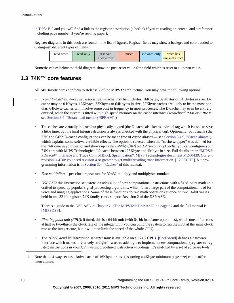
Register diagrams in this book are found in the list of figures. Register fields may show a background color, coded todistinguish different types of fields:
Numeric values below the field diagram show the post-reset value for a field which is reset to a known value.
1.3 74K™ core features
All 74K family cores conform to Release 2 of the MIPS32 architecture. You may have the following options:
• I- and D-Caches: 4-way set associative; I-cache may be 0 Kbytes, 16Kbytes, 32Kbytes or 64Kbytes in size. D-cache may be 0 Kbytes, 16Kbytes, 32Kbytes or 64Kbytes in size. 32Kbyte caches are likely to be the most pop-ular; 64Kbyte caches will involve some cost in frequency in most processes. The D-cache may even be entirelyomitted, when the system is fitted with high-speed memory on the cache interface (scratchpad RAM or SPRAM:see Section 3.6 “Scratchpad memory/SPRAM”.)
• The caches are virtually indexed but physically tagged (the D-cache also keeps a virtual tag which is used to savea little time, but the final hit/miss decision is always checked with the physical tag). Optionally (but usually) the
32K and 64K2 D-cache configurations can be made free of cache aliases — see Section 3.4.9, "Cache aliases",which explains some software-visible effects. The option is selected when the “cache wrapper” was defined forthe 74K core in your design and shows up as the Config7[AR] bit. L2 (secondary) cache: you can configure your74K core with MIPS Technologies’ L2 cache between 128Kbyte and 1Mbyte in size. Full details are in “MIPS®PDtrace™ Interface and Trace Control Block Specification”, MIPS Technologies document MD00439. Currentrevision is 4.30: you need revision 4 or greater to get multithreading trace information. [L2CACHE], but pro-gramming information is in Section 3.4 “Caches” of this manual.
• Fast multiplier: 1-per-clock repeat rate for 32×32 multiply and multiply/accumulate.
• DSP ASE: this instruction set extension adds a lot of new computational instructions with a fixed-point math unitcrafted to speed up popular signal-processing algorithms, which form a large part of the computational load forvoice and imaging applications. Some of these functions do two math operations at once on two 16-bit valuesheld in one 32-bit register. 74K family cores support Revision 2 of the DSP ASE.
There’s a guide to the DSP ASE in Chapter 7, “The MIPS32® DSP ASE” on page 87 and the full manual is[MIPSDSP].
• Floating point unit (FPU): if fitted, this is a 64-bit unit (with 64-bit load/store operations), which most often runsat half or two-thirds the clock rate of the integer unit (you can build the system to run the FPU at the same clockrate as the integer core, but it will then limit the speed of the whole CPU).
• The “CorExtend®” instruction set extension: is available on all 74K CPUs. [CorExtend] defines a hardwareinterface which makes it relatively straightforward to add logic to implement new computational (register-to-reg-ister) instructions in your CPU, using predefined instruction encodings. It’s matched by a set of software tools
read-write read-only reserved,always zero
unused software-only write hasunusual effect.
2. Note that a 4-way set associative cache of 16Kbyte or less (assuming a 4Kbyte minimum page size) can’t sufferfrom aliases.
1.4 A brief guide to the 74K™ core implementation
Programming the MIPS32® 74K™ Core Family, Revision 02.14 14
Copyright © 2007, 2008, 2010, 2011 MIPS Technologies Inc. All rights reserved.
which allow users to create assembly language mnemonics and C macros for the new instructions. But there’svery little about the CorExtend ASE in this manual.
1.4 A brief guide to the 74K™ core implementation
The 74K family is based around a long (14-19 stage) pipeline with dual issue, and executes instructions out-of-orderto maintain progress around short-term dependencies. The longer pipeline allows for a higher frequency than can bereached by 24K® family cores (in a comparable process), and the more sophisticated instruction scheduling meansthat the 74K core also gets more work done per cycle.
Long-pipeline CPUs can trip up on dependencies (they need a result from a previous instruction), on branches (theydon’t know where to fetch the next instructions until the branch instruction is substantially complete), and on loads(even on cache hits, the data cannot be available for some number of instructions). Earlier MIPS Technologies coreshad no real trouble with dependencies (dependent instructions, in almost all cases, can run in consecutive cycles).That’s not so in the longer-pipeline 74K core, and its key trick to get around dependencies is out-of-order execution.But the techniques used to deal with branches and loads still include branch prediction, non-blocking loads and latewrites — all familiar from MIPS Technologies’ 24K and 34K® core families.
Figure 1.1 Overview of The 74K™ Pipeline
1.4.1 Notes on pipeline overview diagram (Figure 1.1):
Although this diagram is considerably simpler (and further abstracted from reality) than those in [SUM], there is stilla lot to digest. Rectangles and circles with a thick outline are major functional units — the rectangles are the active
I-cache
IFU
IDU
x4 x4 x2
BHT
D-cache
ALUAGEN
GRU
x2
renamemap
loads. stores, etc
out-of-order execution
speculativefetch
issue
in-ordercompletion
completion buffers
read dataexternalread/write
cache miss dataupdatesreg
file
IT ID IS IB DD DR DS DMAF AM AC AB
EM EA EC ES EB
WB GC74K pipeline stages
memory pipeline
Introduction
15 Programming the MIPS32® 74K™ Core Family, Revision 02.14
Copyright © 2007, 2008, 2010, 2011 MIPS Technologies Inc. All rights reserved.
units and each has a phrase (in italics) summarizing what it does. The three-letter acronyms match those found in thedetailed descriptions, and the pipeline stage names used in the detailed descriptions are across the top. To simplify thepicture the integer multiply unit and the (optional) floating point unit have been omitted — once you figure out what’sgoing on, they shouldn’t be too hard to put back. So:
• The 74K core’s instruction fetch unit (“IFU”) is semi-autonomous. It’s 128 bits wide, and handles four instruc-tions at a bite.
The IFU works a bit like a dog being taken for a walk. It rushes on ahead as long as the lead will stretch (the IFU,processing instructions four at a time, can rapidly get ahead). Even though you’re in charge, your dog likes to gofirst - and so it is with the IFU. Like a dog, the IFU guesses where you want to go, strongly influenced by the wayyou usually go. If you make an unexpected turn there is a brief hiatus while the dog comes back and gets up frontagain.
The IFU has a queue to keep instructions in when it’s running ahead of the rest of the CPU. This kind of design iscalled a “decoupled” IFU.
• Issue: the IDU (“instruction decode/dispatch unit”) keeps its own queue of instructions and tries to find two ofthem which can be issued in parallel. The instruction set is strictly divided into AGEN instructions (loads, stores,prefetch, cacheops; conditional moves, branches and jumps) and ALU (everything else). If all else is good, theIDU can issue one instruction of each type in every cycle. Instructions are marked with their place in the programsequence, but are not necessarily issued in order. An instruction may leapfrog ahead of program order in theIDU’s queue, if all the data it needs is ready (or at least will be ready by the time it’s needed).
Instructions which execute ahead of time can’t write data to real registers — that would disrupt the operation oftheir program predecessors, which might execute later. It may turn out that such an instruction shouldn’t have runat all if there was a mispredicted branch, or an earlier-in-program-order instruction took an exception. Instead,each instruction is assigned a completion buffer (CB) entry to receive its result. The CB entry also keeps informa-tion about the instruction and where it came from. An instruction which is dependent on this one for a source reg-ister value but runs soon afterward can get its data from the CB. CB-resident values can be found through therename map; that map is indexed by register number and points to the CB reserved by the instruction which willwrite or has written a register value.
• out-of-order execution: the effect of the above is that instructions are issued in “dataflow” order, as determined bytheir dependencies on register values produced by other instructions. Up to 32 instructions can be somewherebetween available for issue and completed in the 74K core — those instructions are often said to be in flight. The32 possible instructions correspond to 32 CB entries — 14 for AGEN instructions, 18 for ALU instructions.
Inside the “execution” box the AGEN and ALU instructions proceed strictly through two internally-pipelinedunits of the same names. The two pipelines are in lockstep, and are kept that way. This sounds rigid, but is help-ful. When the IDU issues an instruction, it does not have to know that an instruction’s data is ready “right now”:it’s enough that the instruction producing that data is far enough along either execution pipeline. When no otherprogress can be made its probably best to think of the IDU issuing a “no-op” or “bubble” into either or both pipe-lines.
Most of the time the execution pipelines just keep running — the IDU tries to detect any reason why an instruc-tion cannot run through either the AGEN or ALU pipe.When dependent instructions run close together, the datadoesn’t have time to go into a register or CB entry and be read out again. Instead it can flow down a dedicatedbypass connection between two particular pipestages — a routine trick used in pipelined logic. In the 74K corethere are bypasses interconnecting the AGEN and ALU pipelines, as well as within each pipeline. But whereaspipeline multiplexing in a conventional design is controlled by comparing register numbers, in 74K cores wecompare completion buffer entry IDs.
1.4 A brief guide to the 74K™ core implementation
Programming the MIPS32® 74K™ Core Family, Revision 02.14 16
Copyright © 2007, 2008, 2010, 2011 MIPS Technologies Inc. All rights reserved.
There are a few simple instructions where the ALU produces its results in one clock (they’re listed in Table 4.3),but most ALU instructions require two clocks: so, in the 74K core, dependent ALU instructions cannot usuallybe run back-to-back. This would have a catastrophic effect on the performance of an in-order CPU, becausemany instructions are dependent on their immediate predecessor. But an out-of-order CPU will run just fine,because there are also a reasonable number of cases where an instruction is not dependent on its immediate pre-decessor, so the pipeline can find something to run. The CPU will slow down if fed with a sequence of relativelylong-latency instructions each of which is dependent on its predecessor, of course. For example, in the AGENpipeline it takes four cycles to turn a load address into load data (assuming a cache hit). So chasing a chain ofpointers through memory will take at least four cycles per pointer.
• Optimistic issue: any instruction which is issued may yet not run to completion (there might be an exception onan earlier-in-program instruction, for example). But some instructions are issued even though they are directlydependent on something we’re not sure about — they’re issued optimistically. The most common example is thatinstructions dependent on load data are issued as if we were confident the load will hit in the L1 cache.
Sometimes it turns out we were wrong. Notably, sometimes the load we’re dependent on suffers a cache miss. Inthis case the hardware does the simplest thing: rather than attempt to single out the now unviable instruction, wetake a redirect on the load-value-consuming instruction we issued optimistically — that is, we discard all workon that instruction and its successors, and ask the front end of the pipeline to start again from scratch, re-fetchingthe instruction from the I-cache.
• In-order completion: at the end of the execution unit we take the oldest in-flight instruction (with luck, the sec-
ond-oldest too) and, if it’s results are ready, we graduate3 one or two instructions (“GRU” stands for “graduationunit”). Before we do that, we make a last minute check for exceptions: if one of the proposed graduates hasencountered a condition which should cause an exception it will be carrying that information with it, we discardthat instruction and do a redirect to the start of the appropriate exception handler. On successful graduation theinstruction’s results are copied from its CB entry back to a real CPU register, and it’s finished.
Because instruction effects aren’t “publicly” visible until graduation, our out-of-order CPU appears to the pro-grammer to be running sequentially just like any other MIPS32-compliant CPU.
More details about out-of-order execution
That’s the basic flow. But the dual-issue, out-of-order design has some subtle points which can affect how programsrun:
• Mispredicted branches and redirects: because of the long pipeline, the 74K core relies very heavily on goodbranch prediction. When the IFU guesses wrong about a conditional branch, or can’t compute the target for ajump-register instruction, that’s detected somewhere down the AGEN pipeline (usually the “EC” stage). By thenwe’ll have done a minimum of 12 cycles of work on the wrong path.
Whenever a branch is resolved the prediction result is sent back to the IFU to maintain its history table. For mostbranches, the prediction result is sent back at the same time as we resolve the branch, which means that a fewbranches which don’t graduate can affect the branch history. That’s OK, it was only a heuristic.
• Exceptions: can’t be resolved until we’re committed to running an instruction and have completed all its prede-cessors. So they’re resolved only at graduation. That posts an exception handler address down to the front of apipe, clearing out all prefetched and speculatively-executed instructions in the process. There will be at least 19
3. Curiously, the alternative word to “graduation” (for an instruction being committed in an out-of-order design) is “retirement”:a rather different stage of one’s career. I guess that from a software point of view we’re glad that the instruction is now grownup and real, while the hardware is now ready to wave goodbye to it.
Introduction
17 Programming the MIPS32® 74K™ Core Family, Revision 02.14
Copyright © 2007, 2008, 2010, 2011 MIPS Technologies Inc. All rights reserved.
cycles between the point where the exception is processed in the graduation unit and the time when the firstinstruction of the exception handler graduates.
• Loads and Stores: the L1 cache lookup happens inside the out-of-order execution pipeline. But only loads whichhit in the L1 cache are complete when they graduate. Other loads and stores graduate and then start actions in thememory pipeline. It’s probably fairly obvious how a store can be “stored” — so long as the hardware keeps a noteof the address and data of the store, the cache/memory update can be done later. On the 74K core, even a writeinto the L1 cache is deferred until after graduation. While the write is pending, the cache hardware has to keep anote in case some later instruction wants to load the same value before we’ve completed the write; but that’sfamiliar technology.
It’s less obvious that we can allow load instructions which L1-miss to graduate. But on the 74K core, loads arenon-blocking — a load executes, and results in data being loaded into a GP register at some time in the future.Any later instruction which reads the register value must wait until the load data has arrived. So load instructionsare allowed to graduate regardless of how far away their data is. Once the instruction graduates its CB entry mustbe given back, so data arriving for a graduated load is sent directly to the register file.
There’s another key reason why we did this: with only L1 accesses done out-of-order, loads and stores onlybecome visible outside the CPU after they graduate, so there’s no worry about other parts of the system seeingunexpected effects from speculative instructions.
An instruction which depends on a load which misses will (unless it was a long, long way behind in instructionsequence) have to wait. Most often the consuming instruction will become a candidate for issue before we knowwhether the load hit in the L1 cache. In this case the dependent instruction is issued: we’re optimists, hoping fora hit. If a consuming instruction reaches graduation and finds the load missed, we must do a “redirect”, re-fetch-ing the consuming instruction and everything later in program order). Next time the consuming instruction is anissue candidate, we’ll know the load has missed, and the consumer will not get issued until the load data hasarrived. The redirect for the consuming instruction is quite expensive (19 or more cycles), but in most cases thatoverhead will be hidden in the time taken to return data for the cache miss.
Stores are less complicated. But since even the cache must not be updated until the store instruction graduates,the memory pipeline is used for writing the L1 cache too: even store L1-hits result in action in the memory pipe-line.
1.4.2 Branches and branch delays
The MIPS architecture defines that the instruction following a branch (the “branch delay slot” instruction) is always
executed4. That means that the CPU has one instruction it knows will be executed while it’s figuring out where abranch is going. But with the 74K core’s long pipeline we don’t finally know whether a conditional branch should betaken, and won’t have computed the target address for a jump-register, until about 8 stages down the pipeline. It’s bet-ter to guess (and pay the price when we’re wrong) than to wait to be certain. Several different tricks are used:
• The decoupled IFU (the electronic dog) runs ahead of the rest of the CPU by fetching four instructions per clock.
• Branch instructions are identified very early (in fact, they’re marked when instructions are fetched into the I–cache). MIPS branch and jump instructions (at least those not dependent on register values) are easy to decode,and the IFU decodes them locally to calculate the target address.
4. That’s not quite accurate: there are special forms of conditional branches called “branch likely” which are defined to executethe branch delay slot instruction only when the branch is taken. Note that the “likely” part of the name has nothing to do withbranch prediction; the 74K core’s branch prediction system treats the “likelies” just like any other branches. The dependencybetween a branch condition and the branch delay slot instruction is annoying to keep track of in an out-of-order machine, andMIPS would prefer you not to use branch-likely instructions.
1.4 A brief guide to the 74K™ core implementation
Programming the MIPS32® 74K™ Core Family, Revision 02.14 18
Copyright © 2007, 2008, 2010, 2011 MIPS Technologies Inc. All rights reserved.
The IFU’s branch predictor guesses whether conditional branches will be taken or not - it’s not magic, it uses aBHT (a “Branch History Table”) of what happened to branches in the past, indexed by the low bits of the loca-tion of the branch instruction. This particular hardware is an example of Combined branch prediction (majorityvoting between three different algorithms, one of which is gshare; if you want to know, there’s a good wikipediaarticle whose topic name is “Branch Predictor”). The branch predictor is taking a good guess. It can seem sur-prising that the predictor makes no attempt to discover whether the history stored in a BHT slot is really that ofthe current branch, or another one which happened to share the same low address bits; we’re going to be wrongsometimes. It guesses correctly most of the time.
In this way the IFU can predict the next-instruction address and continue to run ahead.
• When the IFU guesses wrong, it doesn’t know (the dog just rushes ahead until its owner reaches the fork). Thebranch mispredict will be noticed once the branch instruction has been issued and carried through to the AGEN“EC” stage, and is executed in its full context (“resolved”). On detecting a mispredict, the CPU must discard theinstructions based on the bad guess (which will not have graduated yet, so will not have changed any vital
machine state) and start fetching instructions from the correct target5. The exact penalty paid by a program whichsuffers a mispredict depends on how busy the execution unit is, and how early it resolves the branch; the mini-mum penalty is 12 cycles.
• Even when we guess right, the branch target calculation in the IFU takes a little while to operate. A rapidsequence of correctly-predicted branches can empty the queues, causing a program to run slower.
• Jump-register instruction targets are unpredictable: the IFU has no knowledge of register data and can’t in gen-eral anticipate it. But jump-register instructions are relatively rare, except for subroutine returns. In the MIPSISA you return from subroutines using a jump-register instruction, jr $31 (register 31 is, by a strong conven-tion, used to hold the return address). So on every call instruction, the IFU pushes the return address onto a small
stack; and on every jr $31 it pops the value of the stack and uses that as its guess for the branch target6.
We have no way of knowing the target of a jr instruction which uses a register other than $31. When we findone of those, instruction fetch stops until the correct address is computed up in the AGEN pipeline, 12 or moreclocks later.
1.4.3 Loads and load-to-use delays
Even short-pipeline MIPS CPUs can’t deliver load data to the immediately following instruction without a delay,even on a cache hit. Simple MIPS pipelines typically deliver the data one clock later: a one clock “load-to-use delay”.Compilers and programmers try to put some useful and non-dependent operation between the load and its first use.
The 74K core’s long pipeline means that a full D-cache hit takes four clocks to return the data, not two: that would bea three-clock “load-to-use delay”. A pair of loads dependent on each other (one fetches the other’s base address) mustbe issued at least four cycles apart (that’s optimistic, hoping-for-a-hit timing).
But the AGEN and ALU pipelines are “skewed”, with ALU results delivered a cycle later than AGEN results. Thatmeans that when an ALU operation is dependent on a load, it can be issued only three cycles after the load. There’s aprice to pay: a load/store whose base address is computed by a preceding ALU instruction must be issued a clock
5. In “branch-likely” variants of conditional branch instructions a mispredict means we also did the wrong thing with theinstruction in the branch delay slot. To fix that up, we need to refetch the branch itself, so the penalty is at least one cyclehigher.
6. The return-stack guess will be wrong for subroutines containing nested calls deeper than the size of the return stack; but sub-routines high up the call tree are much more rarely executed, so this isn’t so bad.
Introduction
19 Programming the MIPS32® 74K™ Core Family, Revision 02.14
Copyright © 2007, 2008, 2010, 2011 MIPS Technologies Inc. All rights reserved.
later than an ALU instruction with the same dependency — that’s usually a three cycle delay, because most ALUoperations already take an extra clock to produce their result.
It’s like the skewed pipeline which experts in MIPS Technologies’ 24K® family might remember, and has the samemotivation: ALU operations dependent on recent loads are more common than loads dependent on recent ALU oper-ations.
1.4.4 Queues, Resource limits and Consequences
Queues which can fill up include:
• Cache refills in flight: Is dependent on the size of the “FSB” queue - this and other queues are described in moredetail under Section 3.3, "Reads, writes and synchronization". The CPU does not wait for a cache refill process— at least not until it needs data from the cache miss. But in practice most load data is used almost at once, so theCPU will stop very soon after a miss. As a result, you’re unlikely to ever have four refills in flight unless you areusing prefetch or otherwise deliberately optimizing loops. If a series of aggressive prefetches miss often enough,the fourth outstanding load-miss will use the last FSB entry, preventing further loads from graduating and even-tually blocking up the whole CPU until the load data returns. It’s likely to be good practice for code making con-scious use of prefetches to ration itself to a number of operations slightly less than the size of the FSB.
• Non-blocking loads to registers (nine): there are nine entries in the “LDQ”, each of which remembers one out-standing load, and which register the data is destined to return to. Compiled code is unlikely to reach this limit. Ifyou write carefully optimized code where you try to fill load-use delays (perhaps for data you think will not hit inthe D-cache) you may hit this problem.
• Lines evicted from the cache awaiting writeback (4+): writes are collected in the “WBB” queue. The 74K core’sability to write data will in almost all circumstances exceed the bandwidth available to memory; so a long enoughburst of uncached or write-through writes will eventually slow to memory speed. Otherwise, you’re unlikely tosuffer from this.
• Queues in the coprocessor interface: the 74K core hides its out-of-order character from any coprocessors, socoprocessor hardware need be no more complicated than it is for MIPS Technologies’ 24K core. The coprocessorhardware sees its instructions strictly in order. Each coprocessor instruction also makes its own way through theinteger execution unit. Between the execution unit and coprocessor there are some queues which can fill up:
• IOIQ (8 entries): instructions being issued — strictly in program order — to a coprocessor.
• CBIDQ (8 entries): data being returned from a coprocessor by an instruction which writes a GP register. Butprior to graduation the data goes back to a completion buffer (hence the queue acronym).
• CLDQ (8 entries): track data being loaded to coprocessor registers (the job done for the GPRs by the LDQabove). CLDQ data isn’t necessarily provided in instruction sequence: in particular MIPS Technologiesfloating-point unit accepts FP load data as and when it arrives, making FP loads non-blocking.
The dispatch process stalls (flooding the ALU and AGEN pipes with bubbles) when there is no space in any ofthese queues.
1.4 A brief guide to the 74K™ core implementation
Programming the MIPS32® 74K™ Core Family, Revision 02.14 20
Copyright © 2007, 2008, 2010, 2011 MIPS Technologies Inc. All rights reserved.
Chapter 2
Programming the MIPS32® 74K™ Core Family, Revision 02.14 21
Copyright © 2007, 2008, 2010, 2011 MIPS Technologies Inc. All rights reserved.
Initialization and identity
What happens when the CPU is first powered up? These functions are perhaps more often associated with a ROMmonitor than an OS.
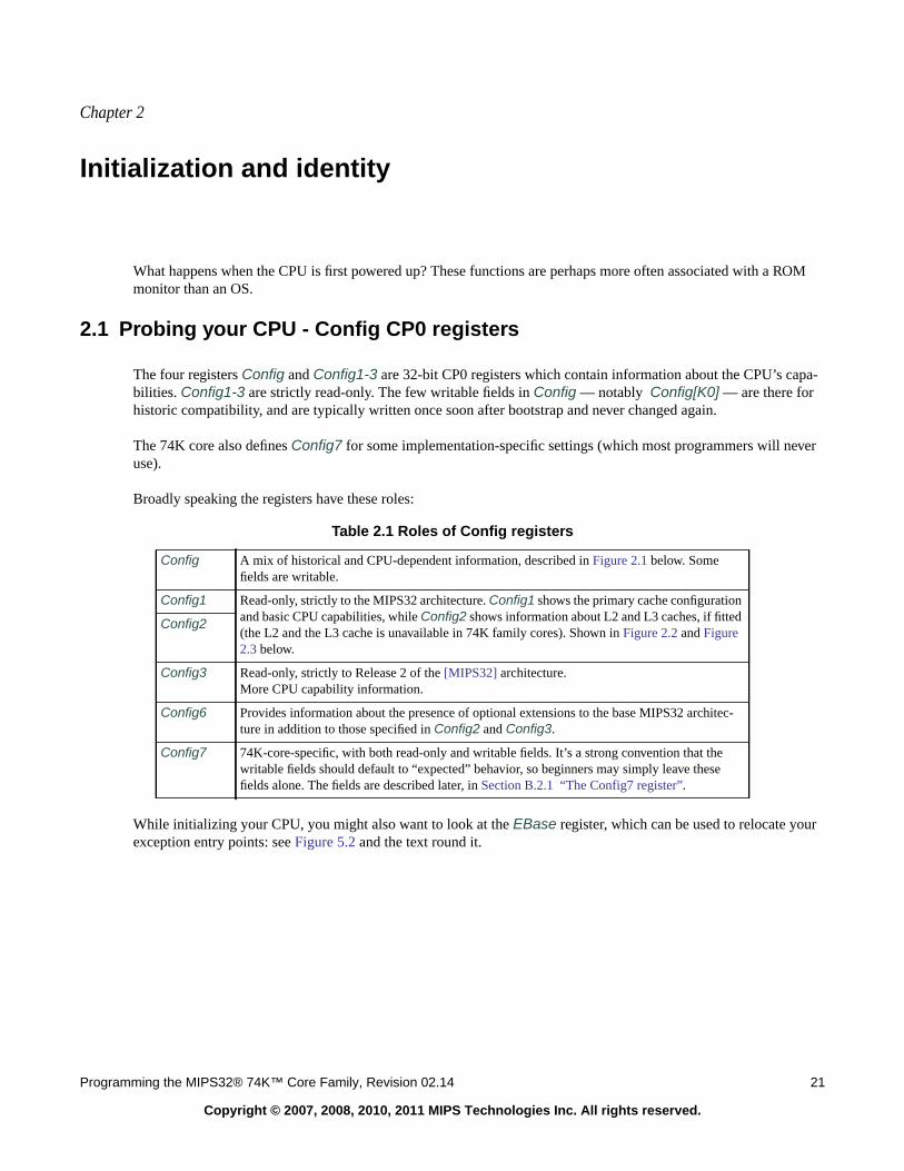
2.1 Probing your CPU - Config CP0 registers
The four registers Config and Config1-3 are 32-bit CP0 registers which contain information about the CPU’s capa-bilities. Config1-3 are strictly read-only. The few writable fields in Config — notably Config[K0] — are there forhistoric compatibility, and are typically written once soon after bootstrap and never changed again.
The 74K core also defines Config7 for some implementation-specific settings (which most programmers will neveruse).
Broadly speaking the registers have these roles:
While initializing your CPU, you might also want to look at the EBase register, which can be used to relocate yourexception entry points: see Figure 5.2 and the text round it.
Table 2.1 Roles of Config registers
Config A mix of historical and CPU-dependent information, described in Figure 2.1 below. Somefields are writable.
Config1 Read-only, strictly to the MIPS32 architecture. Config1 shows the primary cache configurationand basic CPU capabilities, while Config2 shows information about L2 and L3 caches, if fitted(the L2 and the L3 cache is unavailable in 74K family cores). Shown in Figure 2.2 and Figure2.3 below.
Config2
Config3 Read-only, strictly to Release 2 of the [MIPS32] architecture.More CPU capability information.
Config6 Provides information about the presence of optional extensions to the base MIPS32 architec-ture in addition to those specified in Config2 and Config3.
Config7 74K-core-specific, with both read-only and writable fields. It’s a strong convention that thewritable fields should default to “expected” behavior, so beginners may simply leave thesefields alone. The fields are described later, in Section B.2.1 “The Config7 register”.
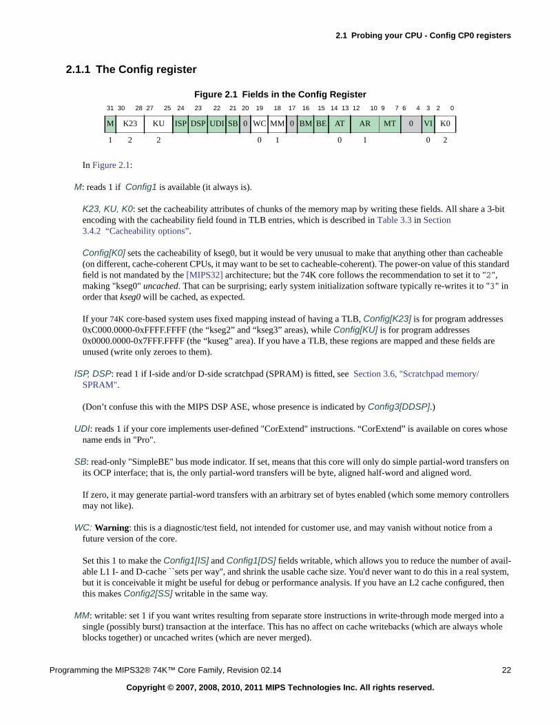
2.1 Probing your CPU - Config CP0 registers
Programming the MIPS32® 74K™ Core Family, Revision 02.14 22
Copyright © 2007, 2008, 2010, 2011 MIPS Technologies Inc. All rights reserved.
2.1.1 The Config register
Figure 2.1 Fields in the Config Register
In Figure 2.1:
M: reads 1 if Config1 is available (it always is).
K23, KU, K0: set the cacheability attributes of chunks of the memory map by writing these fields. All share a 3-bitencoding with the cacheability field found in TLB entries, which is described in Table 3.3 in Section3.4.2 “Cacheability options”.
Config[K0] sets the cacheability of kseg0, but it would be very unusual to make that anything other than cacheable(on different, cache-coherent CPUs, it may want to be set to cacheable-coherent). The power-on value of this standardfield is not mandated by the [MIPS32] architecture; but the 74K core follows the recommendation to set it to "2",making "kseg0" uncached. That can be surprising; early system initialization software typically re-writes it to "3" inorder that kseg0 will be cached, as expected.
If your 74K core-based system uses fixed mapping instead of having a TLB, Config[K23] is for program addresses0xC000.0000-0xFFFF.FFFF (the “kseg2” and “kseg3” areas), while Config[KU] is for program addresses0x0000.0000-0x7FFF.FFFF (the “kuseg” area). If you have a TLB, these regions are mapped and these fields areunused (write only zeroes to them).
ISP, DSP: read 1 if I-side and/or D-side scratchpad (SPRAM) is fitted, see Section 3.6, "Scratchpad memory/SPRAM".
(Don’t confuse this with the MIPS DSP ASE, whose presence is indicated by Config3[DDSP].)
UDI: reads 1 if your core implements user-defined "CorExtend" instructions. “CorExtend” is available on cores whosename ends in "Pro".
SB: read-only "SimpleBE" bus mode indicator. If set, means that this core will only do simple partial-word transfers onits OCP interface; that is, the only partial-word transfers will be byte, aligned half-word and aligned word.
If zero, it may generate partial-word transfers with an arbitrary set of bytes enabled (which some memory controllersmay not like).
WC: Warning: this is a diagnostic/test field, not intended for customer use, and may vanish without notice from afuture version of the core.
Set this 1 to make the Config1[IS] and Config1[DS] fields writable, which allows you to reduce the number of avail-able L1 I- and D-cache ``sets per way'', and shrink the usable cache size. You'd never want to do this in a real system,but it is conceivable it might be useful for debug or performance analysis. If you have an L2 cache configured, thenthis makes Config2[SS] writable in the same way.
MM: writable: set 1 if you want writes resulting from separate store instructions in write-through mode merged into asingle (possibly burst) transaction at the interface. This has no affect on cache writebacks (which are always wholeblocks together) or uncached writes (which are never merged).
31 30 28 27 25 24 23 22 21 20 19 18 17 16 15 14 13 12 10 9 7 6 4 3 2 0
M K23 KU ISP DSP UDI SB 0 WC MM 0 BM BE AT AR MT 0 VI K0
1 2 2 0 1 0 1 0 2
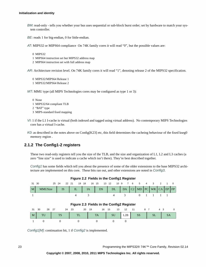
Initialization and identity
23 Programming the MIPS32® 74K™ Core Family, Revision 02.14
Copyright © 2007, 2008, 2010, 2011 MIPS Technologies Inc. All rights reserved.
BM: read-only - tells you whether your bus uses sequential or sub-block burst order; set by hardware to match your sys-tem controller.
BE: reads 1 for big-endian, 0 for little-endian.
AT: MIPS32 or MIPS64 compliance On 74K family cores it will read “0”, but the possible values are:
AR: Architecture revision level. On 74K family cores it will read “1”, denoting release 2 of the MIPS32 specification.
MT: MMU type (all MIPS Technologies cores may be configured as type 1 or 3):
VI: 1 if the L1 I-cache is virtual (both indexed and tagged using virtual address). No contemporary MIPS Technologiescore has a virtual I-cache.
K0: as described in the notes above on Config[K23] etc, this field determines the cacheing behaviour of the fixed kseg0memory region .
2.1.2 The Config1-2 registers
These two read-only registers tell you the size of the TLB, and the size and organization of L1, L2 and L3 caches (azero “line size” is used to indicate a cache which isn’t there). They’re best described together.
Config1 has some fields which tell you about the presence of some of the older extensions to the base MIPS32 archi-tecture are implemented on this core. These bits ran out, and other extensions are noted in Config3.
Figure 2.2 Fields in the Config1 Register
Figure 2.3 Fields in the Config2 Register
Config1[M]: continuation bit, 1 if Config2 is implemented.
0 MIPS321 MIPS64 instruction set but MIPS32 address map2 MIPS64 instruction set with full address map
0 MIPS32/MIPS64 Release 11 MIPS32/MIPS64 Release 2
0 None1 MIPS32/64 compliant TLB2 “BAT” type3 MIPS-standard fixed mapping
31 30 25 24 22 21 19 18 16 15 13 12 10 9 7 6 5 4 3 2 1 0
M MMUSize IS IL IA DS DL DA C2 MD PC WR CA EP FP
1 4 3 4 3 0 1 1 1 1
31 30 28 27 24 23 20 19 16 15 13 12 11 8 7 4 3 0
M TU TS TL TA SU L2B SS SL SA
1 0 0 0 0 0 0
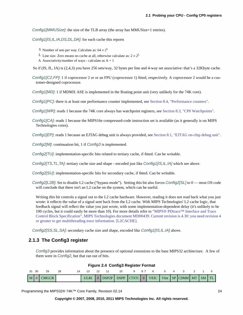
2.1 Probing your CPU - Config CP0 registers
Programming the MIPS32® 74K™ Core Family, Revision 02.14 24
Copyright © 2007, 2008, 2010, 2011 MIPS Technologies Inc. All rights reserved.
Config1[MMUSize]: the size of the TLB array (the array has MMUSize+1 entries).
Config1[IS,IL,IA,DS,DL,DA]: for each cache this reports
So if (IS, IL, IA) is (2,4,3) you have 256 sets/way, 32 bytes per line and 4-way set associative: that’s a 32Kbyte cache.
Config1[C2,FP]: 1 if coprocessor 2 or or an FPU (coprocessor 1) fitted, respectively. A coprocessor 2 would be a cus-tomer-designed coprocessor.
Config1[MD]: 1 if MDMX ASE is implemented in the floating point unit (very unlikely for the 74K core).
Config1[PC]: there is at least one performance counter implemented, see Section 8.4, "Performance counters".
Config1[WR]: reads 1 because the 74K core always has watchpoint registers, see Section 8.3, "CP0 Watchpoints".
Config1[CA]: reads 1 because the MIPS16e compressed-code instruction set is available (as it generally is on MIPSTechnologies cores).
Config1[EP]: reads 1 because an EJTAG debug unit is always provided, see Section 8.1, "EJTAG on-chip debug unit".
Config2[M]: continuation bit, 1 if Config3 is implemented.
Config2[TU]: implementation-specific bits related to tertiary cache, if fitted. Can be writable.
Config2[TS,TL,TA]: tertiary cache size and shape - encoded just like Config1[IS,IL,IA] which see above.
Config2[SU]: implementation-specific bits for secondary cache, if fitted. Can be writable.
Config2[L2B]: Set to disable L2 cache (“bypass mode”). Setting this bit also forces Config2[SL] to 0 — most OS codewill conclude that there isn't an L2 cache on the system, which can be useful.
Writing this bit controls a signal out to the L2 cache hardware. However, reading it does not read back what you justwrote: it reflects the value of a signal sent back from the L2 cache. With MIPS Technologies' L2 cache logic, thatfeedback signal will reflect the value you just wrote, with some implementation-dependent delay (it's unlikely to be100 cycles, but it could easily be more than 10). For more details refer to “MIPS® PDtrace™ Interface and TraceControl Block Specification”, MIPS Technologies document MD00439. Current revision is 4.30: you need revision 4or greater to get multithreading trace information. [L2CACHE].
Config2[SS,SL,SA]: secondary cache size and shape, encoded like Config1[IS,IL,IA] above.
2.1.3 The Config3 register
Config3 provides information about the presence of optional extensions to the base MIPS32 architecture. A few ofthem were in Config2, but that ran out of bits.
Figure 2.4 Config3 Register Format
S Number of sets per way. Calculate as: 64 × 2S
L Line size. Zero means no cache at all, otherwise calculate as: 2 × 2L
A Associativity/number of ways - calculate as A + 1
31 30 29 28 14 13 12 11 10 9 8 7 6 5 4 3 2 1 0
M 0 CMGCR ULRI 0 DSP2P DSPP CTXTC 0 VEIC VInt SP CDMM MT SM TL
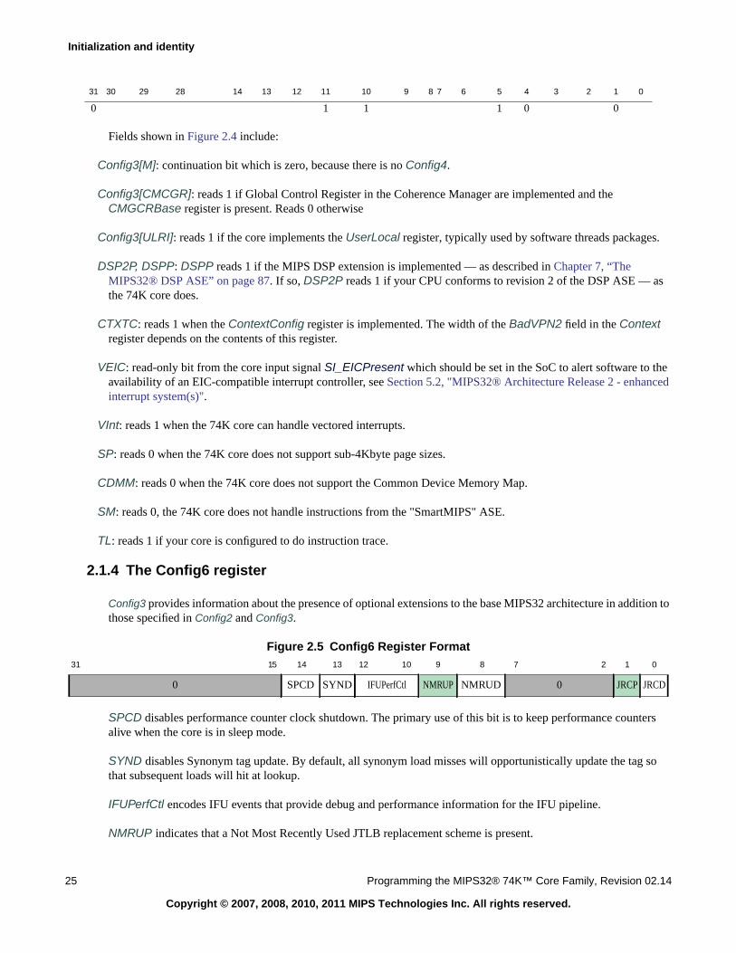
Initialization and identity
25 Programming the MIPS32® 74K™ Core Family, Revision 02.14
Copyright © 2007, 2008, 2010, 2011 MIPS Technologies Inc. All rights reserved.
Fields shown in Figure 2.4 include:
Config3[M]: continuation bit which is zero, because there is no Config4.
Config3[CMCGR]: reads 1 if Global Control Register in the Coherence Manager are implemented and theCMGCRBase register is present. Reads 0 otherwise
Config3[ULRI]: reads 1 if the core implements the UserLocal register, typically used by software threads packages.
DSP2P, DSPP: DSPP reads 1 if the MIPS DSP extension is implemented — as described in Chapter 7, “TheMIPS32® DSP ASE” on page 87. If so, DSP2P reads 1 if your CPU conforms to revision 2 of the DSP ASE — asthe 74K core does.
CTXTC: reads 1 when the ContextConfig register is implemented. The width of the BadVPN2 field in the Contextregister depends on the contents of this register.
VEIC: read-only bit from the core input signal SI_EICPresent which should be set in the SoC to alert software to theavailability of an EIC-compatible interrupt controller, see Section 5.2, "MIPS32® Architecture Release 2 - enhancedinterrupt system(s)".
VInt: reads 1 when the 74K core can handle vectored interrupts.
SP: reads 0 when the 74K core does not support sub-4Kbyte page sizes.
CDMM: reads 0 when the 74K core does not support the Common Device Memory Map.
SM: reads 0, the 74K core does not handle instructions from the "SmartMIPS" ASE.
TL: reads 1 if your core is configured to do instruction trace.
2.1.4 The Config6 register
Config3 provides information about the presence of optional extensions to the base MIPS32 architecture in addition tothose specified in Config2 and Config3.
Figure 2.5 Config6 Register Format
SPCD disables performance counter clock shutdown. The primary use of this bit is to keep performance countersalive when the core is in sleep mode.
SYND disables Synonym tag update. By default, all synonym load misses will opportunistically update the tag sothat subsequent loads will hit at lookup.
IFUPerfCtl encodes IFU events that provide debug and performance information for the IFU pipeline.
NMRUP indicates that a Not Most Recently Used JTLB replacement scheme is present.
0 1 1 1 0 0
31 15 14 13 12 10 9 8 7 2 1 0
0 SPCD SYND IFUPerfCtl NMRUP NMRUD 0 JRCP JRCD
31 30 29 28 14 13 12 11 10 9 8 7 6 5 4 3 2 1 0
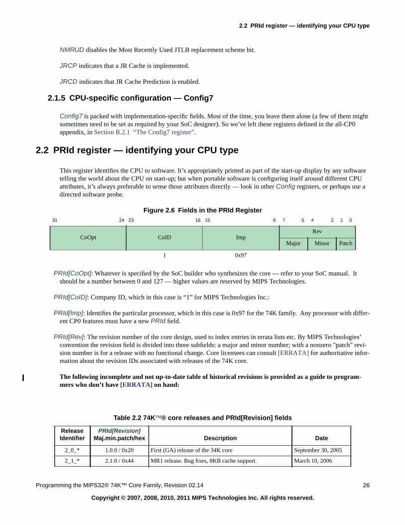
2.2 PRId register — identifying your CPU type
Programming the MIPS32® 74K™ Core Family, Revision 02.14 26
Copyright © 2007, 2008, 2010, 2011 MIPS Technologies Inc. All rights reserved.
NMRUD disables the Most Recently Used JTLB replacement scheme bit.
JRCP indicates that a JR Cache is implemented.
JRCD indicates that JR Cache Prediction is enabled.
2.1.5 CPU-specific configuration — Config7
Config7 is packed with implementation-specific fields. Most of the time, you leave them alone (a few of them mightsometimes need to be set as required by your SoC designer). So we’ve left these registers defined in the all-CP0appendix, in Section B.2.1 “The Config7 register”.
2.2 PRId register — identifying your CPU type
This register identifies the CPU to software. It’s appropriately printed as part of the start-up display by any softwaretelling the world about the CPU on start-up; but when portable software is configuring itself around different CPUattributes, it’s always preferable to sense those attributes directly — look in other Config registers, or perhaps use adirected software probe.
Figure 2.6 Fields in the PRId Register
PRId[CoOpt]: Whatever is specified by the SoC builder who synthesizes the core — refer to your SoC manual. Itshould be a number between 0 and 127 — higher values are reserved by MIPS Technologies.
PRId[CoID]: Company ID, which in this case is “1” for MIPS Technologies Inc.:
PRId[Imp]: Identifies the particular processor, which in this case is 0x97 for the 74K family. Any processor with differ-ent CP0 features must have a new PRId field.
PRId[Rev]: The revision number of the core design, used to index entries in errata lists etc. By MIPS Technologies’convention the revision field is divided into three subfields: a major and minor number; with a nonzero "patch" revi-sion number is for a release with no functional change. Core licensees can consult [ERRATA] for authoritative infor-mation about the revision IDs associated with releases of the 74K core.
The following incomplete and not up-to-date table of historical revisions is provided as a guide to program-mers who don’t have [ERRATA] on hand:
31 24 23 16 15 8 7 5 4 2 1 0
CoOpt CoID ImpRev
Major Minor Patch
1 0x97
Table 2.2 74K™® core releases and PRId[Revision] fields
ReleaseIdentifier
PRId[Revision]Maj.min.patch/hex Description Date
2_0_* 1.0.0 / 0x20 First (GA) release of the 34K core September 30, 2005
2_1_* 2.1.0 / 0x44 MR1 release. Bug fixes, 8KB cache support. March 10, 2006
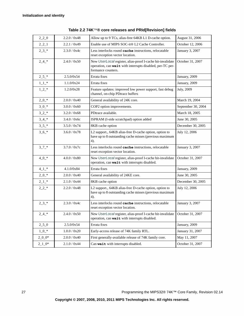
Initialization and identity
27 Programming the MIPS32® 74K™ Core Family, Revision 02.14
Copyright © 2007, 2008, 2010, 2011 MIPS Technologies Inc. All rights reserved.
2_2_0 2.2.0 / 0x48 Allow up to 9 TCs, alias-free 64KB L1 D-cache option. August 31, 2006
2_2_1 2.2.1 / 0x49 Enable use of MIPS SOC-it® L2 Cache Controller. October 12, 2006
2_3_* 2.3.0 / 0x4c Less interlocks round cache instructions, relocatablereset exception vector location.
January 3, 2007
2_4_* 2.4.0 / 0x50 New UserLocal register, alias-proof I-cache hit-invalidateoperation, can wait with interrupts disabled, per-TC per-formance counters.
October 31, 2007
2_5_* 2.5.0/0x54 Errata fixes January, 2009
1_1_* 1.1.0/0x24 Errata fixes January, 2009
1_2_* 1.2.0/0x28 Feature updates: improved low power support, fast debugchannel, on-chip PDtrace buffers
July, 2009
2_0_* 2.0.0 / 0x40 General availability of 24K core. March 19, 2004
3_0_* 3.0.0 / 0x60 COP2 option improvements. September 30, 2004
3_2_* 3.2.0 / 0x68 PDtrace available. March 18, 2005
3_4_* 3.4.0 / 0x6c ISPRAM (I-side scratchpad) option added June 30, 2005
3_5_* 3.5.0 / 0x74 8KB cache option December 30, 2005
3_6_* 3.6.0 / 0x78 L2 support., 64KB alias-free D-cache option, option tohave up to 8 outstanding cache misses (previous maximum4).
July 12, 2006
3_7_* 3.7.0 / 0x7c Less interlocks round cache instructions, relocatablereset exception vector location.
January 3, 2007
4_0_* 4.0.0 / 0x80 New UserLocal register, alias-proof I-cache hit-invalidateoperation, can wait with interrupts disabled.
October 31, 2007
4_1_* 4.1.0/0x84 Errata fixes January, 2009
2_0_* 2.0.0 / 0x40 General availability of 24KE core. June 30, 2005
2_1_* 2.1.0 / 0x44 8KB cache option December 30, 2005
2_2_* 2.2.0 / 0x48 L2 support., 64KB alias-free D-cache option, option tohave up to 8 outstanding cache misses (previous maximum4).
July 12, 2006
2_3_* 2.3.0 / 0x4c Less interlocks round cache instructions, relocatablereset exception vector location.
January 3, 2007
2_4_* 2.4.0 / 0x50 New UserLocal register, alias-proof I-cache hit-invalidateoperation, can wait with interrupts disabled.
October 31, 2007
2_5_0 2.5.0/0x54 Errata fixes January, 2009
1_0_* 1.0.0 / 0x20 Early-access release of 74K family RTL. January 31, 2007
2_0_0* 2.0.0 / 0x40 First generally-available release of 74K family core. May 11, 2007
2_1_0* 2.1.0 / 0x44 Can wait with interrupts disabled. October 31, 2007
Table 2.2 74K™® core releases and PRId[Revision] fields
2.2 PRId register — identifying your CPU type
Programming the MIPS32® 74K™ Core Family, Revision 02.14 28
Copyright © 2007, 2008, 2010, 2011 MIPS Technologies Inc. All rights reserved.
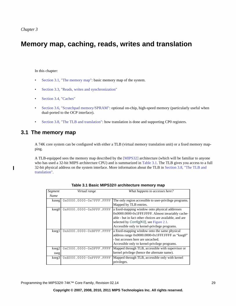
Chapter 3
Programming the MIPS32® 74K™ Core Family, Revision 02.14 29
Copyright © 2007, 2008, 2010, 2011 MIPS Technologies Inc. All rights reserved.
Memory map, caching, reads, writes and translation
In this chapter:
• Section 3.1, "The memory map": basic memory map of the system.
• Section 3.3, "Reads, writes and synchronization"
• Section 3.4, "Caches"
• Section 3.6, "Scratchpad memory/SPRAM": optional on-chip, high-speed memory (particularly useful whendual-ported to the OCP interface).
• Section 3.8, "The TLB and translation": how translation is done and supporting CP0 registers.
3.1 The memory map
A 74K core system can be configured with either a TLB (virtual memory translation unit) or a fixed memory map-ping.
A TLB-equipped sees the memory map described by the [MIPS32] architecture (which will be familiar to anyonewho has used a 32-bit MIPS architecture CPU) and is summarized in Table 3.1. The TLB gives you access to a full32-bit physical address on the system interface. More information about the TLB in Section 3.8, "The TLB andtranslation".
Table 3.1 Basic MIPS32® architecture memory mapSegment Virtual range What happens to accesses here?
Namekuseg 0x0000.0000-0x7FFF.FFFF The only region accessible to user-privilege programs.
Mapped by TLB entries.kseg0 0x8000.0000-0x9FFF.FFFF a fixed-mapping window onto physical addresses
0x0000.0000-0x1FFF.FFFF. Almost invariably cache-able - but in fact other choices are available, and areselected by Config[K0], see Figure 2.1.Accessible only to kernel-privilege programs.
kseg1 0xA000.0000-0xBFFF.FFFF a fixed-mapping window onto the same physicaladdress range 0x0000.0000-0x1FFF.FFFF as “kseg0”- but accesses here are uncached.Accessible only to kernel-privilege programs.
kseg2 0xC000.0000-0xDFFF.FFFF Mapped through TLB, accessible with supervisor orkernel privilege (hence the alternate name).sseg
kseg3 0xE000.0000-0xFFFF.FFFF Mapped through TLB, accessible only with kernelprivileges.
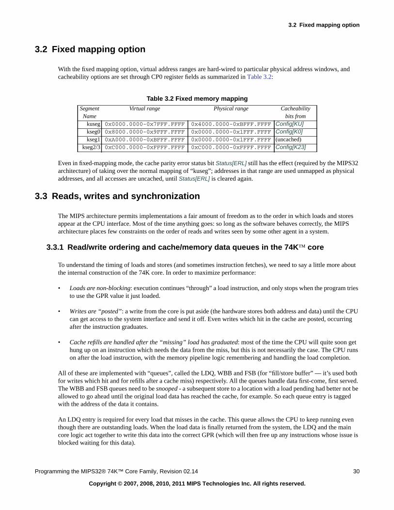
3.2 Fixed mapping option
Programming the MIPS32® 74K™ Core Family, Revision 02.14 30
Copyright © 2007, 2008, 2010, 2011 MIPS Technologies Inc. All rights reserved.
3.2 Fixed mapping option
With the fixed mapping option, virtual address ranges are hard-wired to particular physical address windows, andcacheability options are set through CP0 register fields as summarized in Table 3.2:
Even in fixed-mapping mode, the cache parity error status bit Status[ERL] still has the effect (required by the MIPS32architecture) of taking over the normal mapping of “kuseg”; addresses in that range are used unmapped as physicaladdresses, and all accesses are uncached, until Status[ERL] is cleared again.
3.3 Reads, writes and synchronization
The MIPS architecture permits implementations a fair amount of freedom as to the order in which loads and storesappear at the CPU interface. Most of the time anything goes: so long as the software behaves correctly, the MIPSarchitecture places few constraints on the order of reads and writes seen by some other agent in a system.
3.3.1 Read/write ordering and cache/memory data queues in the 74K™ core
To understand the timing of loads and stores (and sometimes instruction fetches), we need to say a little more aboutthe internal construction of the 74K core. In order to maximize performance:
• Loads are non-blocking: execution continues “through” a load instruction, and only stops when the program triesto use the GPR value it just loaded.
• Writes are “posted”: a write from the core is put aside (the hardware stores both address and data) until the CPUcan get access to the system interface and send it off. Even writes which hit in the cache are posted, occurringafter the instruction graduates.
• Cache refills are handled after the “missing” load has graduated: most of the time the CPU will quite soon gethung up on an instruction which needs the data from the miss, but this is not necessarily the case. The CPU runson after the load instruction, with the memory pipeline logic remembering and handling the load completion.
All of these are implemented with “queues”, called the LDQ, WBB and FSB (for “fill/store buffer” — it’s used bothfor writes which hit and for refills after a cache miss) respectively. All the queues handle data first-come, first served.The WBB and FSB queues need to be snooped - a subsequent store to a location with a load pending had better not beallowed to go ahead until the original load data has reached the cache, for example. So each queue entry is taggedwith the address of the data it contains.
An LDQ entry is required for every load that misses in the cache. This queue allows the CPU to keep running eventhough there are outstanding loads. When the load data is finally returned from the system, the LDQ and the maincore logic act together to write this data into the correct GPR (which will then free up any instructions whose issue isblocked waiting for this data).
Table 3.2 Fixed memory mappingSegment Virtual range Physical range Cacheability
Name bits fromkuseg 0x0000.0000-0x7FFF.FFFF 0x4000.0000-0xBFFF.FFFF Config[KU]kseg0 0x8000.0000-0x9FFF.FFFF 0x0000.0000-0x1FFF.FFFF Config[K0]kseg1 0xA000.0000-0xBFFF.FFFF 0x0000.0000-0x1FFF.FFFF (uncached)
kseg2/3 0xC000.0000-0xFFFF.FFFF 0xC000.0000-0xFFFF.FFFF Config[K23]
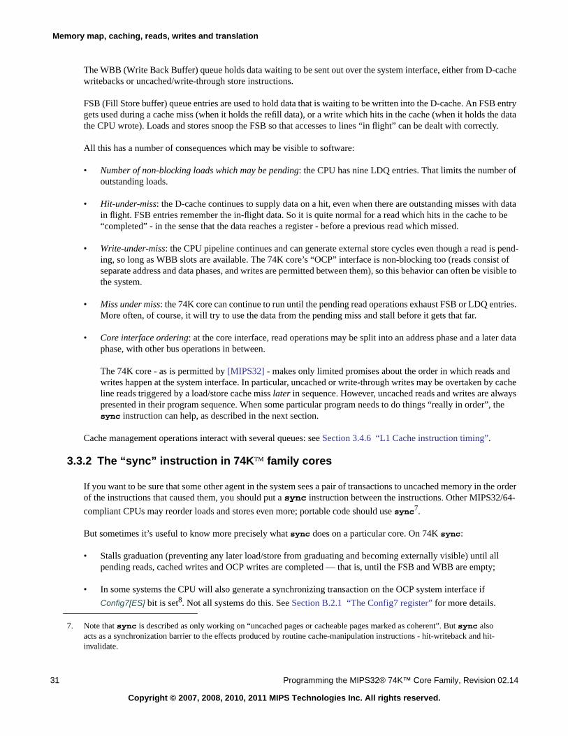
Memory map, caching, reads, writes and translation
31 Programming the MIPS32® 74K™ Core Family, Revision 02.14
Copyright © 2007, 2008, 2010, 2011 MIPS Technologies Inc. All rights reserved.
The WBB (Write Back Buffer) queue holds data waiting to be sent out over the system interface, either from D-cachewritebacks or uncached/write-through store instructions.
FSB (Fill Store buffer) queue entries are used to hold data that is waiting to be written into the D-cache. An FSB entrygets used during a cache miss (when it holds the refill data), or a write which hits in the cache (when it holds the datathe CPU wrote). Loads and stores snoop the FSB so that accesses to lines “in flight” can be dealt with correctly.
All this has a number of consequences which may be visible to software:
• Number of non-blocking loads which may be pending: the CPU has nine LDQ entries. That limits the number ofoutstanding loads.
• Hit-under-miss: the D-cache continues to supply data on a hit, even when there are outstanding misses with datain flight. FSB entries remember the in-flight data. So it is quite normal for a read which hits in the cache to be“completed” - in the sense that the data reaches a register - before a previous read which missed.
• Write-under-miss: the CPU pipeline continues and can generate external store cycles even though a read is pend-ing, so long as WBB slots are available. The 74K core’s “OCP” interface is non-blocking too (reads consist ofseparate address and data phases, and writes are permitted between them), so this behavior can often be visible tothe system.
• Miss under miss: the 74K core can continue to run until the pending read operations exhaust FSB or LDQ entries.More often, of course, it will try to use the data from the pending miss and stall before it gets that far.
• Core interface ordering: at the core interface, read operations may be split into an address phase and a later dataphase, with other bus operations in between.
The 74K core - as is permitted by [MIPS32] - makes only limited promises about the order in which reads andwrites happen at the system interface. In particular, uncached or write-through writes may be overtaken by cacheline reads triggered by a load/store cache miss later in sequence. However, uncached reads and writes are alwayspresented in their program sequence. When some particular program needs to do things “really in order”, thesync instruction can help, as described in the next section.
Cache management operations interact with several queues: see Section 3.4.6 “L1 Cache instruction timing”.
3.3.2 The “sync” instruction in 74K™ family cores
If you want to be sure that some other agent in the system sees a pair of transactions to uncached memory in the orderof the instructions that caused them, you should put a sync instruction between the instructions. Other MIPS32/64-
compliant CPUs may reorder loads and stores even more; portable code should use sync7.
But sometimes it’s useful to know more precisely what sync does on a particular core. On 74K sync:
• Stalls graduation (preventing any later load/store from graduating and becoming externally visible) until allpending reads, cached writes and OCP writes are completed — that is, until the FSB and WBB are empty;
• In some systems the CPU will also generate a synchronizing transaction on the OCP system interface if
Config7[ES] bit is set8. Not all systems do this. See Section B.2.1 “The Config7 register” for more details.
7. Note that sync is described as only working on “uncached pages or cacheable pages marked as coherent”. But sync alsoacts as a synchronization barrier to the effects produced by routine cache-manipulation instructions - hit-writeback and hit-invalidate.
3.4 Caches
Programming the MIPS32® 74K™ Core Family, Revision 02.14 32
Copyright © 2007, 2008, 2010, 2011 MIPS Technologies Inc. All rights reserved.
A new set of lightweight SYNC instructions have been introduced. As compared to the completion barrier, the order-ing barrier is a lighter-weight operation as it does not require the specified instructions before the SYNC to be alreadycompleted. Instead it only requires that those specified instructions which are subsequent to the SYNC in the instruc-tion stream are never re-ordered for processing ahead of the specified instructions which are before the SYNC in theinstruction stream. This potentially reduces how many cycles the barrier instruction must stall before it completes.
Because the core processes loads and stores in order, ordering barriers are much lighter weight. Details about the setof supported lightweight SYNC instructions can be found in the Software User’s Reference Manual
3.3.3 Write gathering and “write buffer flushing” in 74K™ family cores
We mentioned above that writes to the system (whether uncached writes or cache write-backs) are performed some-what lazily, the write being held in the WBB queue until a convenient moment. That can have two system-visibleeffects:
• Writes can happen later than you think. Your write will happen before the next uncached read or write, but that’sall you know. And your write might still be posted somewhere in a system controller, unless you know your sys-tem is built to prevent it. Sometimes it’s better to code a dummy uncached read from a nearby location (whichwill “flush out” buffered writes on pretty much any system).
• If your cache is configured for write-through, then cached writes to locations in the same “cache line”-sizedchunk of memory may be gathered - stored together in the WBB, and then dealt with by a single “wider” OCPwrite than the one you originally coded. Sometimes, this is what you want. When it isn’t, put a sync betweenyour successive writes. Regular uncached writes are never merged, but special “uncached accelerated” writesmay be — see Section 3.4.3 below.
3.4 Caches
Most of the time caches just work and are invisible to software... though your programs would go twenty times slowerwithout them. But this section is about when caches aren’t invisible any more.
Like most modern MIPS CPUs, the 74K core has separate primary I- and D-caches. They are virtually-indexed andphysically-tagged, so you may need to deal with cache aliases, see Section 3.4.9, "Cache aliases". The design pro-vides for 16Kbyte, 32Kbyte or 64Kbyte caches; but the largest of those are likely to come with some speed penalty.The 74K core’s primary caches are 4-way set associative.
Your 74K core can optionally be built with a L2 (level 2 or secondary) cache. see section below for details.
But don’t hard-wire any of this information into your software. Instead, probe the Config1 register defined by[MIPS32] (and described in ) to determine the shape and size of the L1 and any L2 cache.
3.4.1 The L2 cache option
The L2 cache is an option available to your SoC builder. Basic facts and figures:
• The L2 cache is attached to the core’s standard 64-bit OCP system interface, and when you fit it everything elseis attached to the core through the L2 cache, which has a system-side interface for that purpose. The core-side
8. This will be a read with the signal OC_MReqInfo[3] set. Handling of this transaction is system dependent, but a typical sys-tem controller will flush any external write buffers and complete all pending transactions before telling the CPU that thetransaction is completed. Ask your system integrator how it works in your SoC.
Memory map, caching, reads, writes and translation
33 Programming the MIPS32® 74K™ Core Family, Revision 02.14
Copyright © 2007, 2008, 2010, 2011 MIPS Technologies Inc. All rights reserved.
interface is enhanced and augmented to support cache instructions targeted at the L2, and to carry back perfor-mance counter information and so on.
• The L2 ‘s size can be 128Kbytes, 256Kbytes, 512Kbytes or 1Mbyte. However, there are options which allow theSoC builder to have one or more of the ways of the cache memory array visible as normal system memoryinstead. There’s very little in this manual about that option. — see “MIPS® PDtrace™ Interface and TraceControl Block Specification”, MIPS Technologies document MD00439. Current revision is 4.30: you needrevision 4 or greater to get multithreading trace information. [L2CACHE].
• The L2 cache is indexed and tagged with the physical address, so is unaffected by cache aliases.
• Cache lines are either 32 bytes long (matching the L1 caches) or 64 bytes. The L2 cache’s memories are accessed256 bits at a time internally, though it has 64-bit interfaces.
• It can be configured with 4-way or 8-way set-associative organization. In a 4-way cache the line replacement pol-icy is “least recently used” (LRU); true LRU is impractical for an 8-way set associative cache, so something sim-pler (a “pseudo-LRU”) is used.
• The cache has an option for error detection and correction. 1-bit data errors can be corrected and all 2-bit errorsdetected with an 8-bit-per-doubleword ECC field. Check bits are provided on cache tags, too. If your L2 has ECCfitted, ErrCtl[L2P] will be writable — see Section 3.4.17 “ErrCtl register” for details.
• The cache is write-back but does not allocate a line on a write miss (write miss data is just sent directly to the sys-tem memory). It is write-through for memory regions which request that policy -- see Section3.4.2 “Cacheability options” for details.
• The L2 cache can run synchronously to the CPU core, but (particularly for memory arrays larger than256Kbytes) would typically then be the critical path for timing. It will more often use a 1:2 or 2:3 clock ratio.The L2’s far-side OCP interface may run at any of a wide range of ratios from the L2 clock down.
• In an effort to keep everything going the cache manages multiple outstanding transactions (it can handle as manyas 15 outstanding misses). Misses are resolved and responses sent as they happen, not in the order of presenta-tion.
• Latency: the L2 logic allows the memory access to be pipelined, a reasonable choice for larger or slower arrays:ask your SoC builder. The L2 delivers hit data in a burst of four 64-bit doublewords. The first doublewordappears after 9 or 10 L2 clocks (10 for pipelined-array systems) and the rest of the burst follows on consecutiveclocks. Added to this is some extra time taken for the original L1 miss to be discovered, synchronizing to the L2clock, and returning the data to the CPU: typically, add 5 CPU clocks.
An L2 miss is slightly more expensive than an L1 miss from the same memory, since we don’t start the memoryaccess until we’ve discovered that the data isn’t in the L2. The L2 memory interface can be configured to be 64-bit or 256-bit wide. An L2 miss will deliver miss data to the CPU core in burst of four 64-bit doublewords.Because the CPU connects to the rest of the system through the L2 cache, it also adds 4 L2 cycles to the latencyof all transactions which bypass the L2.
• The L2 cache requires software management, and you can apply the same cache instructions to it as to the L1 D-cache.
3.4.2 Cacheability options
Any read or write made by the 74K core will be cacheable or not according to the virtual memory map. For addressestranslated by the TLB the cacheability is determined by the TLB entry; the key field appears as EntryLo[C]. Table 3.3
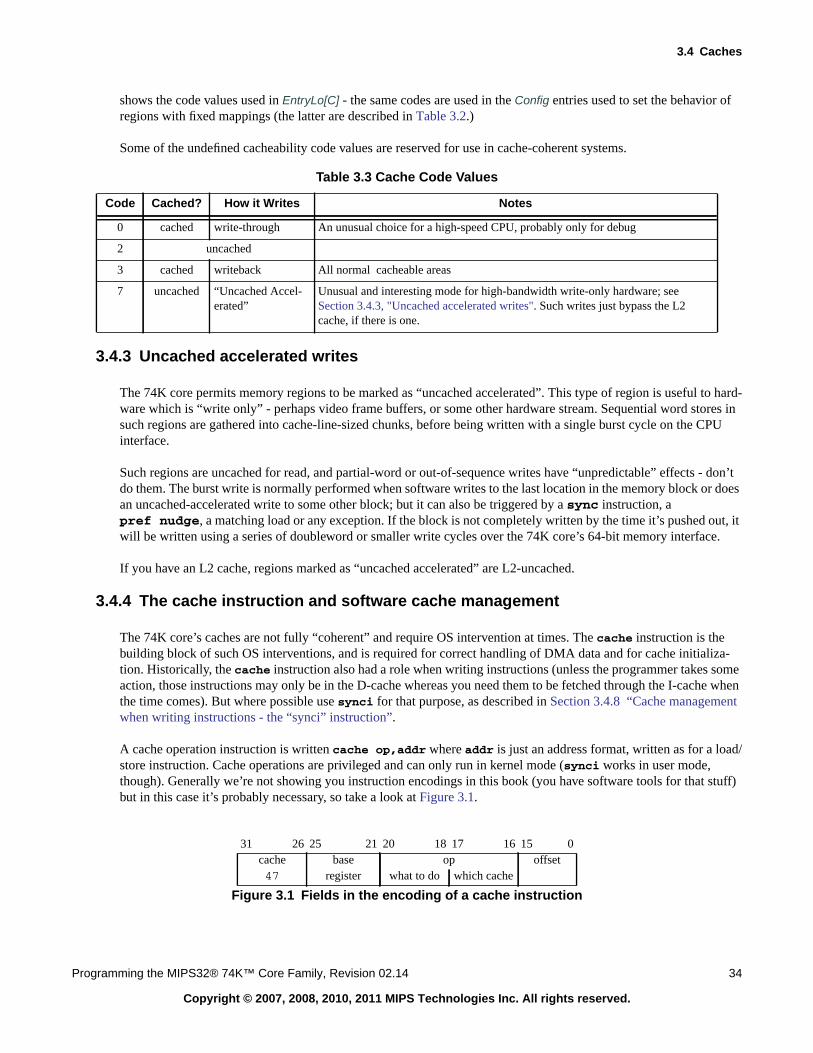
3.4 Caches
Programming the MIPS32® 74K™ Core Family, Revision 02.14 34
Copyright © 2007, 2008, 2010, 2011 MIPS Technologies Inc. All rights reserved.
shows the code values used in EntryLo[C] - the same codes are used in the Config entries used to set the behavior ofregions with fixed mappings (the latter are described in Table 3.2.)
Some of the undefined cacheability code values are reserved for use in cache-coherent systems.
3.4.3 Uncached accelerated writes
The 74K core permits memory regions to be marked as “uncached accelerated”. This type of region is useful to hard-ware which is “write only” - perhaps video frame buffers, or some other hardware stream. Sequential word stores insuch regions are gathered into cache-line-sized chunks, before being written with a single burst cycle on the CPUinterface.
Such regions are uncached for read, and partial-word or out-of-sequence writes have “unpredictable” effects - don’tdo them. The burst write is normally performed when software writes to the last location in the memory block or doesan uncached-accelerated write to some other block; but it can also be triggered by a sync instruction, apref nudge, a matching load or any exception. If the block is not completely written by the time it’s pushed out, itwill be written using a series of doubleword or smaller write cycles over the 74K core’s 64-bit memory interface.
If you have an L2 cache, regions marked as “uncached accelerated” are L2-uncached.
3.4.4 The cache instruction and software cache management
The 74K core’s caches are not fully “coherent” and require OS intervention at times. The cache instruction is thebuilding block of such OS interventions, and is required for correct handling of DMA data and for cache initializa-tion. Historically, the cache instruction also had a role when writing instructions (unless the programmer takes someaction, those instructions may only be in the D-cache whereas you need them to be fetched through the I-cache whenthe time comes). But where possible use synci for that purpose, as described in Section 3.4.8 “Cache managementwhen writing instructions - the “synci” instruction”.
A cache operation instruction is written cache op,addr where addr is just an address format, written as for a load/store instruction. Cache operations are privileged and can only run in kernel mode (synci works in user mode,though). Generally we’re not showing you instruction encodings in this book (you have software tools for that stuff)but in this case it’s probably necessary, so take a look at Figure 3.1.
Table 3.3 Cache Code Values
Code Cached? How it Writes Notes
0 cached write-through An unusual choice for a high-speed CPU, probably only for debug
2 uncached
3 cached writeback All normal cacheable areas
7 uncached “Uncached Accel-erated”
Unusual and interesting mode for high-bandwidth write-only hardware; seeSection 3.4.3, "Uncached accelerated writes". Such writes just bypass the L2cache, if there is one.
31 26 25 21 20 18 17 16 15 0cache base op offset47 register what to do which cache
Figure 3.1 Fields in the encoding of a cache instruction
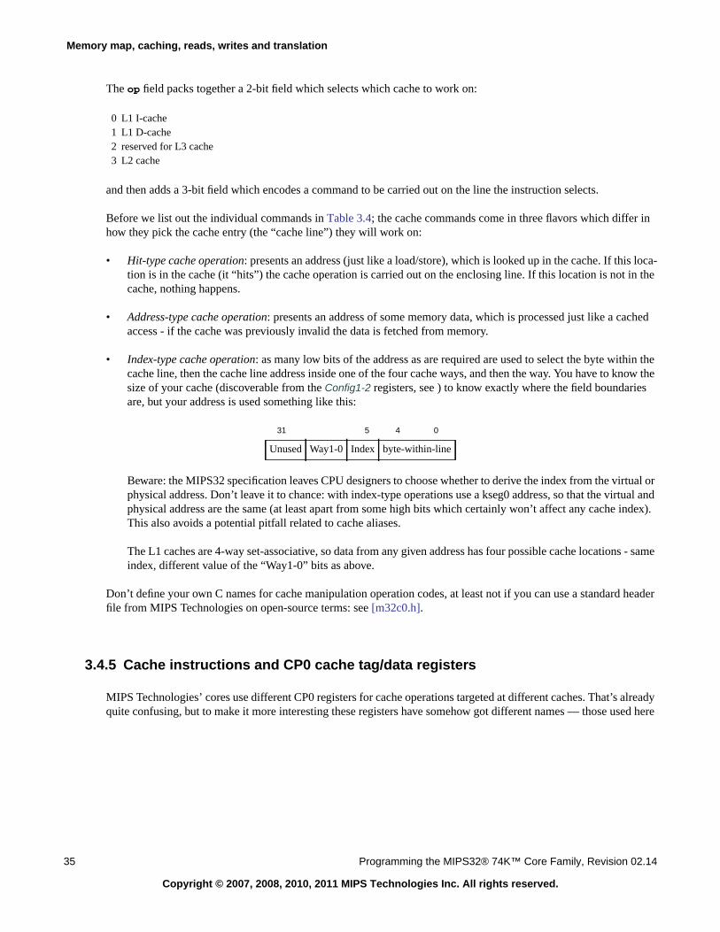
Memory map, caching, reads, writes and translation
35 Programming the MIPS32® 74K™ Core Family, Revision 02.14
Copyright © 2007, 2008, 2010, 2011 MIPS Technologies Inc. All rights reserved.
The op field packs together a 2-bit field which selects which cache to work on:
and then adds a 3-bit field which encodes a command to be carried out on the line the instruction selects.
Before we list out the individual commands in Table 3.4; the cache commands come in three flavors which differ inhow they pick the cache entry (the “cache line”) they will work on:
• Hit-type cache operation: presents an address (just like a load/store), which is looked up in the cache. If this loca-tion is in the cache (it “hits”) the cache operation is carried out on the enclosing line. If this location is not in thecache, nothing happens.
• Address-type cache operation: presents an address of some memory data, which is processed just like a cachedaccess - if the cache was previously invalid the data is fetched from memory.
• Index-type cache operation: as many low bits of the address as are required are used to select the byte within thecache line, then the cache line address inside one of the four cache ways, and then the way. You have to know thesize of your cache (discoverable from the Config1-2 registers, see ) to know exactly where the field boundariesare, but your address is used something like this:
Beware: the MIPS32 specification leaves CPU designers to choose whether to derive the index from the virtual orphysical address. Don’t leave it to chance: with index-type operations use a kseg0 address, so that the virtual andphysical address are the same (at least apart from some high bits which certainly won’t affect any cache index).This also avoids a potential pitfall related to cache aliases.
The L1 caches are 4-way set-associative, so data from any given address has four possible cache locations - sameindex, different value of the “Way1-0” bits as above.
Don’t define your own C names for cache manipulation operation codes, at least not if you can use a standard headerfile from MIPS Technologies on open-source terms: see [m32c0.h].
3.4.5 Cache instructions and CP0 cache tag/data registers
MIPS Technologies’ cores use different CP0 registers for cache operations targeted at different caches. That’s alreadyquite confusing, but to make it more interesting these registers have somehow got different names — those used here
0 L1 I-cache1 L1 D-cache2 reserved for L3 cache3 L2 cache
31 5 4 0
Unused Way1-0 Index byte-within-line
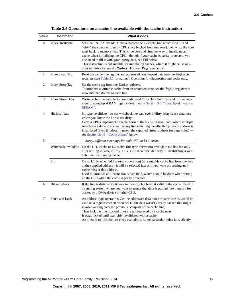
3.4 Caches
Programming the MIPS32® 74K™ Core Family, Revision 02.14 36
Copyright © 2007, 2008, 2010, 2011 MIPS Technologies Inc. All rights reserved.
Table 3.4 Operations on a cache line available with the cache instruction
Value Command What it does
0 Index invalidate Sets the line to “invalid”. If it’s a D-cache or L2 cache line which is valid and“dirty” (has been written by CPU since fetched from memory), then write the con-tents back to memory first. This is the best and simplest way to invalidate an I-cache when initializing the CPU - though if your cache is parity-protected, youalso need to fill it with good-parity data, see Fill below.This instruction is not suitable for initializing caches, where it might cause ran-dom write-backs: see the Index Store Tag type below.
1 Index Load Tag Read the cache line tag bits and addressed doubleword data into the TagLo etcregisters (see Table 3.1 for names). Operation for diagnostics and geeks only.
2 Index Store Tag Set the cache tag from the TagLo registers.To initialize a writable cache from an unknown state, set the TagLo registers tozero and then do this to each line.
3 Index Store Data Write cache-line data. Not commonly used for caches, but it is used for manage-ment of scratchpad RAM regions described in Section 3.6 “Scratchpad memory/SPRAM”.
4 Hit invalidate hit-type invalidate - do not writeback the data even if dirty. May cause data lossunless you know the line is not dirty.Certain CPUs implement a special form of the I-side hit invalidate, where multiplesearches are done to ensure that any line matching the effective physical address isinvalidated (even if it doesn’t match the supplied virtual address for page color) —see Section 3.4.9 “Cache aliases” below.
5 Sorry, different meanings for code “5” on L1 I-cache.
Writeback invalidate On the L1D-cache or L2 cache: (hit-type operation) invalidate the line but onlyafter writing it back, if dirty. This is the recommended way of invalidating a writ-able line in a running cache.
Fill On an L1 I-cache: (address-type operation) fill a suitable cache line from the dataat the supplied address - it will be selected just as if you were processing an I-cache miss at this address.Used to initialize an I-cache line’s data field, which should be done when settingup the CPU when the cache is parity protected.
6 Hit writeback If the line is dirty, write it back to memory but leave it valid in the cache. Used ina running system where you want to ensure that data is pushed into memory foraccess by a DMA device or other CPU.
7 Fetch and Lock An address-type operation. Get the addressed data into the same line as would beused on a regular cached reference (if the data wasn’t already cached that mightinvolve writing back the previous occupant of the cache line).Then lock the line. Locked lines are not replaced on a cache miss.It stays locked until explicitly invalidated with a cacheAn attempt to lock the last entry available at some particular index fails silently.
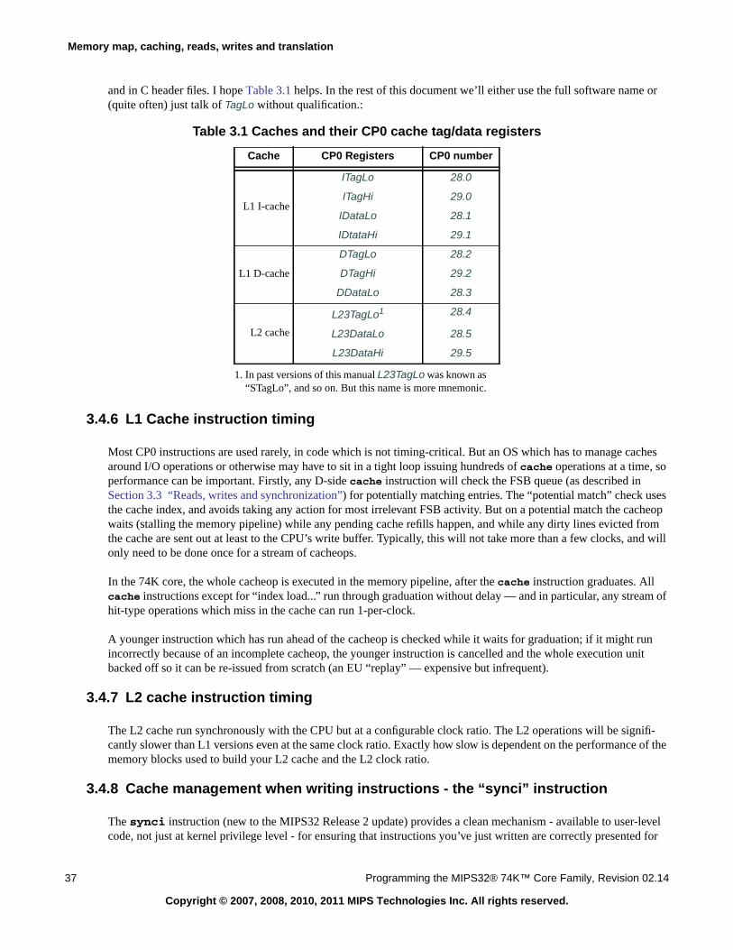
Memory map, caching, reads, writes and translation
37 Programming the MIPS32® 74K™ Core Family, Revision 02.14
Copyright © 2007, 2008, 2010, 2011 MIPS Technologies Inc. All rights reserved.
and in C header files. I hope Table 3.1 helps. In the rest of this document we’ll either use the full software name or(quite often) just talk of TagLo without qualification.:
3.4.6 L1 Cache instruction timing
Most CP0 instructions are used rarely, in code which is not timing-critical. But an OS which has to manage cachesaround I/O operations or otherwise may have to sit in a tight loop issuing hundreds of cache operations at a time, soperformance can be important. Firstly, any D-side cache instruction will check the FSB queue (as described inSection 3.3 “Reads, writes and synchronization”) for potentially matching entries. The “potential match” check usesthe cache index, and avoids taking any action for most irrelevant FSB activity. But on a potential match the cacheopwaits (stalling the memory pipeline) while any pending cache refills happen, and while any dirty lines evicted fromthe cache are sent out at least to the CPU’s write buffer. Typically, this will not take more than a few clocks, and willonly need to be done once for a stream of cacheops.
In the 74K core, the whole cacheop is executed in the memory pipeline, after the cache instruction graduates. Allcache instructions except for “index load...” run through graduation without delay — and in particular, any stream ofhit-type operations which miss in the cache can run 1-per-clock.
A younger instruction which has run ahead of the cacheop is checked while it waits for graduation; if it might runincorrectly because of an incomplete cacheop, the younger instruction is cancelled and the whole execution unitbacked off so it can be re-issued from scratch (an EU “replay” — expensive but infrequent).
3.4.7 L2 cache instruction timing
The L2 cache run synchronously with the CPU but at a configurable clock ratio. The L2 operations will be signifi-cantly slower than L1 versions even at the same clock ratio. Exactly how slow is dependent on the performance of thememory blocks used to build your L2 cache and the L2 clock ratio.
3.4.8 Cache management when writing instructions - the “synci” instruction
The synci instruction (new to the MIPS32 Release 2 update) provides a clean mechanism - available to user-levelcode, not just at kernel privilege level - for ensuring that instructions you’ve just written are correctly presented for
Table 3.1 Caches and their CP0 cache tag/data registers
Cache CP0 Registers CP0 number
L1 I-cache
ITagLo 28.0
ITagHi 29.0
IDataLo 28.1
IDtataHi 29.1
L1 D-cache
DTagLo 28.2
DTagHi 29.2
DDataLo 28.3
L2 cache
L23TagLo1
1. In past versions of this manual L23TagLo was known as“STagLo”, and so on. But this name is more mnemonic.
28.4
L23DataLo 28.5
L23DataHi 29.5
3.4 Caches
Programming the MIPS32® 74K™ Core Family, Revision 02.14 38
Copyright © 2007, 2008, 2010, 2011 MIPS Technologies Inc. All rights reserved.
execution (it combines a D-cache writeback with an I-cache invalidate). You should use it in preference to the tradi-tional alternative of a D-cache writeback followed by an I-cache invalidate.
synci does nothing to an L2 cache — the L2 cache is unified, and there’s no need to do anything special there tomake data visible for instruction fetch.
3.4.9 Cache aliases
The 74K has L1 caches which are virtually indexed but physically tagged. Since it’s quite routine to have multiplevirtual mappings of the same physical data, it’s possible for such a cache to end up with two copies of the same data.That becomes troublesome:
• When you want to write the data: if a line is stored in two places, you’ll only update one of them and some datawill be lost (at least, there’s a 50% chance it will be lost!) This is obviously disastrous: systems generally workhard to avoid aliases in the D-cache.
• When you want to invalidate the line in the cache: there’s a danger you might invalidate one copy but not theother. This (more subtle) problem can affect the I-cache too.
It can be worked around. There’s no problem for different virtual mappings which generate the same cache index;those lines will all compete for the 4 ways at that index, and then be correctly identified through the physical tag.
The 74K CPU’s smallest page size is 4Kbytes, that’s 212 bytes. The paged memory translation means that the low 12bits of a virtual address is always reproduced in the physical address. Since a 16Kbyte, 4-way set-associative, cachegets its index from the low 12 bits of the address, the 16Kbyte cache is alias-free. In general, you can’t get aliases ifeach cache “way” is no larger than the page size.
In 32Kbyte and 64Kbyte caches, one or two top bits used for the index are not necessarily the same as the correspond-ing bits of the physical address, and aliases are possible. The value of the one or two critical virtual address bits issometimes called the page color.
It’s possible for software to avoid aliases if it can ensure that where multiple virtual mappings to a physical page exist,they all have the same color. An OS can do that by enforcing virtual-memory alignment rules (to at least a 16Kbyteboundary) for shareable regions. It turns out this is practicable over a large range of OS activities: sharing code andlibraries, and deliberate interprocess shared memory. It is not so easy to do in other circumstances, particularly when
pages to be mapped start their life as buffers for some disk or network operation9...
So the 74K contains logic to make a 32Kbyte or 64Kbyte D-cache alias-free (effectively one or two index bits arefrom the physical address, and used late in the cache access process to maintain performance). This logic is a buildoption, and Config7[AR] flag should read 1 if your was built to have an alias-free D-cache.
A 32Kbyte or 64Kbyte I-cache is subject to aliases. It’s not immediately obvious why this matters; you certainly can’tend up losing writes, as you might in an alias-prone D-cache. But I-cache aliases can lead to unexpected events whenyou deliberately invalidate some cache content using the cache instruction. An invalidation directed at one virtualaddress translated to a particular physical line may leave an undesirable valid copy of the same physical data indexedby a virtual alias of a different color. To solve this, some 74K s are built to strengthen hit-type I-cache invalidateinstructions (those include hit-type cache instructions and the synci instruction), so as to guarantee that no copy ofthe addressed physical line remains in the cache. This facility is available if the Config7[IAR] bit reads 1; but if it’s
9. There’s a fair amount of rather ugly code in the MIPS Linux kernel to work around aliases. D-cache aliases (in particular) aredealt with at the cost of quite a large number of extra invalidate operations.
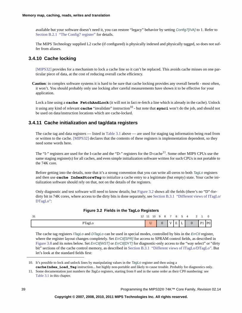
Memory map, caching, reads, writes and translation
39 Programming the MIPS32® 74K™ Core Family, Revision 02.14
Copyright © 2007, 2008, 2010, 2011 MIPS Technologies Inc. All rights reserved.
available but your software doesn’t need it, you can restore “legacy” behavior by setting Config7[IVA] to 1. Refer toSection B.2.1 “The Config7 register” for details.
The MIPS Technology supplied L2 cache (if configured) is physically indexed and physically tagged, so does not suf-fer from aliases.
3.4.10 Cache locking
[MIPS32] provides for a mechanism to lock a cache line so it can’t be replaced. This avoids cache misses on one par-ticular piece of data, at the cost of reducing overall cache efficiency.
Caution: in complex software systems it is hard to be sure that cache locking provides any overall benefit - most often,it won’t. You should probably only use locking after careful measurements have shown it to be effective for yourapplication.
Lock a line using a cache FetchAndLock (it will not in fact re-fetch a line which is already in the cache). Unlock
it using any kind of relevant cache “invalidate” instruction10 - but note that synci won’t do the job, and should notbe used on data/instruction locations which are cache-locked.
3.4.11 Cache initialization and tag/data registers
The cache tag and data registers — listed in Table 3.1 above — are used for staging tag information being read fromor written to the cache. [MIPS32] declares that the contents of these registers is implementation dependent, so theyneed some words here.
The “I-” registers are used for the I-cache and the “D-” registers for the D-cache11. Some other MIPS CPUs use thesame staging register(s) for all caches, and even simple initialization software written for such CPUs is not portable tothe 74K core.
Before getting into the details, note that it’s a strong convention that you can write all-zeros to both TagLo registersand then use cache IndexStoreTag to initialize a cache entry to a legitimate (but empty) state. Your cache ini-tialization software should rely on that, not on the details of the registers.
Only diagnostic and test software will need to know details; but Figure 3.2 shows all the fields (there’s no “D”-for-dirty bit in 74K cores, where access to the dirty bits is done separately, see Section B.3.1 “Different views of ITagLo/DTagLo”:
Figure 3.2 Fields in the TagLo Registers
The cache tag registers ITagLo and DTagLo can be used in special modes, controlled by bits in the ErrCtl register,where the register layout changes completely. Set ErrCtl[SPR] for access to SPRAM control fields, as described inFigure 3.8 and its notes below. Set ErrCtl[WST] or ErrCtl[DYT] for diagnostic-only access to the “way select” or “dirtybit” sections of the cache control memory, as described in Section B.3.1 “Different views of ITagLo/DTagLo”. Butlet’s look at the standard fields first:
10. It’s possible to lock and unlock lines by manipulating values in the TagLo register and then using acacheIndex_Load_Tag instruction... but highly non-portable and likely to cause trouble. Probably for diagnostics only.
11. Some documentation just numbers the TagLo registers, starting from 0 and in the same order as their CP0 numbering: seeTable 3.1 in this chapter.
31 12 11 10 9 8 7 6 5 4 2 1 0
PTagLo U 0 V E L 0 P1 P0
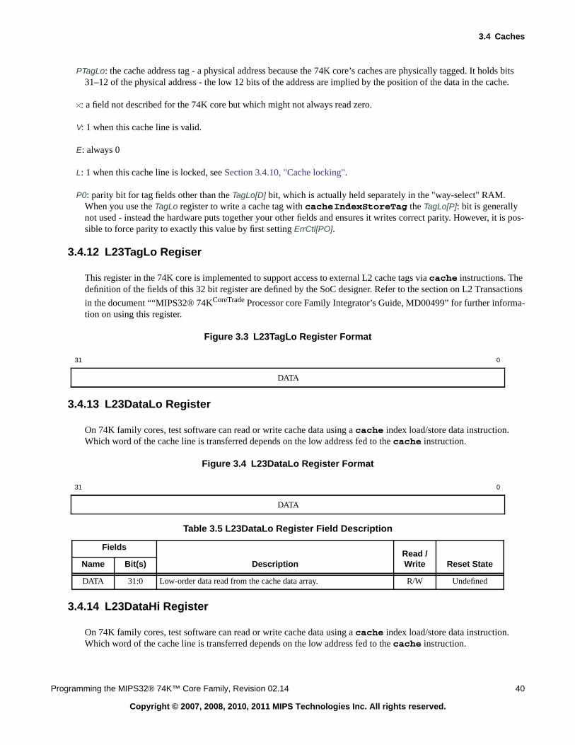
3.4 Caches
Programming the MIPS32® 74K™ Core Family, Revision 02.14 40
Copyright © 2007, 2008, 2010, 2011 MIPS Technologies Inc. All rights reserved.
PTagLo: the cache address tag - a physical address because the 74K core’s caches are physically tagged. It holds bits31–12 of the physical address - the low 12 bits of the address are implied by the position of the data in the cache.
×: a field not described for the 74K core but which might not always read zero.
V: 1 when this cache line is valid.
E: always 0
L: 1 when this cache line is locked, see Section 3.4.10, "Cache locking".
P0: parity bit for tag fields other than the TagLo[D] bit, which is actually held separately in the "way-select" RAM.When you use the TagLo register to write a cache tag with cacheIndexStoreTag the TagLo[P]: bit is generallynot used - instead the hardware puts together your other fields and ensures it writes correct parity. However, it is pos-sible to force parity to exactly this value by first setting ErrCtl[PO].
3.4.12 L23TagLo Regiser
This register in the 74K core is implemented to support access to external L2 cache tags via cache instructions. Thedefinition of the fields of this 32 bit register are defined by the SoC designer. Refer to the section on L2 Transactions
in the document ““MIPS32® 74KCoreTrade Processor core Family Integrator’s Guide, MD00499” for further informa-tion on using this register.
Figure 3.3 L23TagLo Register Format
3.4.13 L23DataLo Register
On 74K family cores, test software can read or write cache data using a cache index load/store data instruction.Which word of the cache line is transferred depends on the low address fed to the cache instruction.
Figure 3.4 L23DataLo Register Format
3.4.14 L23DataHi Register
On 74K family cores, test software can read or write cache data using a cache index load/store data instruction.Which word of the cache line is transferred depends on the low address fed to the cache instruction.
31 0
DATA
31 0
DATA
Table 3.5 L23DataLo Register Field Description
Fields
DescriptionRead /Write Reset StateName Bit(s)
DATA 31:0 Low-order data read from the cache data array. R/W Undefined
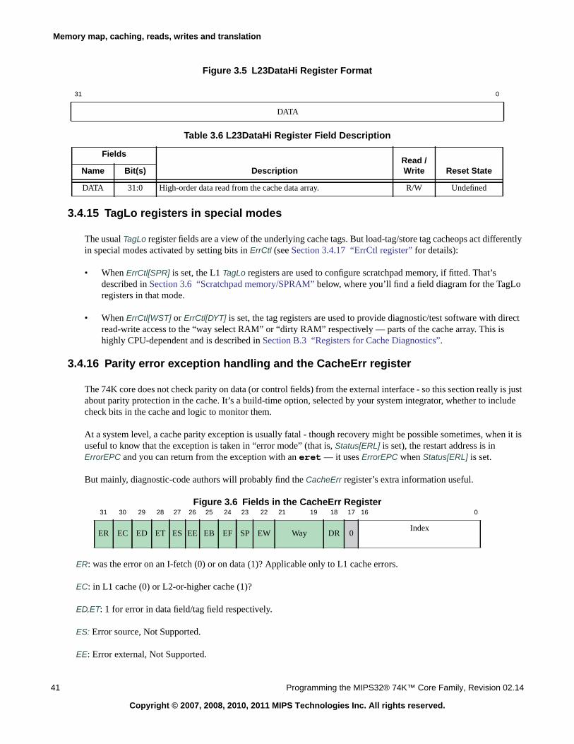
Memory map, caching, reads, writes and translation
41 Programming the MIPS32® 74K™ Core Family, Revision 02.14
Copyright © 2007, 2008, 2010, 2011 MIPS Technologies Inc. All rights reserved.
Figure 3.5 L23DataHi Register Format
3.4.15 TagLo registers in special modes
The usual TagLo register fields are a view of the underlying cache tags. But load-tag/store tag cacheops act differentlyin special modes activated by setting bits in ErrCtl (see Section 3.4.17 “ErrCtl register” for details):
• When ErrCtl[SPR] is set, the L1 TagLo registers are used to configure scratchpad memory, if fitted. That’sdescribed in Section 3.6 “Scratchpad memory/SPRAM” below, where you’ll find a field diagram for the TagLoregisters in that mode.
• When ErrCtl[WST] or ErrCtl[DYT] is set, the tag registers are used to provide diagnostic/test software with directread-write access to the “way select RAM” or “dirty RAM” respectively — parts of the cache array. This ishighly CPU-dependent and is described in Section B.3 “Registers for Cache Diagnostics”.
3.4.16 Parity error exception handling and the CacheErr register
The 74K core does not check parity on data (or control fields) from the external interface - so this section really is justabout parity protection in the cache. It’s a build-time option, selected by your system integrator, whether to includecheck bits in the cache and logic to monitor them.
At a system level, a cache parity exception is usually fatal - though recovery might be possible sometimes, when it isuseful to know that the exception is taken in “error mode” (that is, Status[ERL] is set), the restart address is inErrorEPC and you can return from the exception with an eret — it uses ErrorEPC when Status[ERL] is set.
But mainly, diagnostic-code authors will probably find the CacheErr register’s extra information useful.
Figure 3.6 Fields in the CacheErr Register
ER: was the error on an I-fetch (0) or on data (1)? Applicable only to L1 cache errors.
EC: in L1 cache (0) or L2-or-higher cache (1)?
ED,ET: 1 for error in data field/tag field respectively.
ES: Error source, Not Supported.
EE: Error external, Not Supported.
31 0
DATA
Table 3.6 L23DataHi Register Field Description
Fields
DescriptionRead /Write Reset StateName Bit(s)
DATA 31:0 High-order data read from the cache data array. R/W Undefined
31 30 29 28 27 26 25 24 23 22 21 19 18 17 16 0
ER EC ED ET ES EE EB EF SP EW Way DR 0Index
3.4 Caches
Programming the MIPS32® 74K™ Core Family, Revision 02.14 42
Copyright © 2007, 2008, 2010, 2011 MIPS Technologies Inc. All rights reserved.
EB: 1 if data and instruction-fetch error reported on same instruction, which is unrecoverable. If so, the rest of the regis-ter reports on the instruction-fetch error.
On an L2 error: 1 if an error occurred in more than one of the cache's memory arrays if EC is also set— the hardwaremanual [SUM] renames this field as CacheErr[EM]. The rest of the register can only reflect information about one ofthe errors: it shows tag errors as highest priority, then data, then way-select.
EF: unrecoverable (fatal) error (other than the EB type above). Some parity errors can be fixed by invalidating the cacheline and relying on good data from memory. But if this bit is set, all is lost... It’s one of the following:
1. Line being displaced from cache (“victim”) has a tag parity error, so we don’t know whether to write it back,or whether the writeback location (which needs a correct tag) would be correct.
2. The victim’s tag indicates it has been written by the CPU since it was obtained from memory (the line is“dirty” and needs a write-back), but it has a data parity error.
3. Writeback store miss and CacheErr[EW] error.
4. At least one more cache parity error happened concurrently with or after this one, but before we reached therelative safety of the cache parity error exception handler.
If the EC bit is set this bit is referring to the errors in L2 (external) cache.
SP: error affecting a scratchpad RAM access, see Section 3.6, "Scratchpad memory/SPRAM" below.
EW: parity error on the “dirty” (cache modified) or way-selection bits. This means loss of LRU information, which —most of the time — is recoverable.
Way: the way-number of the cache entry where the error occurred. Caution: for the L1 caches (which are no more than4-way set associative) this is a two-bit field. But an L2 cache might be more highly set-associative, and then this fieldgrows down. In particular, MIPS’ (possibly 8-way set associative) L2 cache uses a 3-bit Way field as shown.
DR: A 1 bit indicates that the reported error affected the cache line "dirty" bits.
Index: the index (within the cache way) of the cache entry where the error occurred... except that the low bits are notmeaningful. The index is aligned as if it’s a byte address, which is good because that’s what Index-type cacheinstructions need. It resolves the failing doubleword for a data error, or just the failing line for a tag error. We’veshown a 14-bit field, because that’s large enough to provide the index for the 74K core’s largest configurable (4 waysby 16KB) L1 cache option.
Two other fields are related to the processing of cache errors. Other implementations have laid claim to all of the bitsin this register, so these bits were relegated to the ErrCtl register. The FE and SE bits in that register are used to detectnested cache errors and are described in the next section.
If you want to study this error further, you’ll probably use an index-type cache instruction to read out the tags and/or data. The cache instruction’s “index” needs the way-number bits added to CacheErr[Index]’s contents; see Figure3.1 and its notes above for how to do that.
3.4.17 ErrCtl register
This register has two distinct roles. It contains “mode bits” which provide different views of the TagLo registers whenthey’re used for access to internal memory arrays and cache diagnostics. But it also controls parity protection of thecaches (if it was configured in your core in the first place).
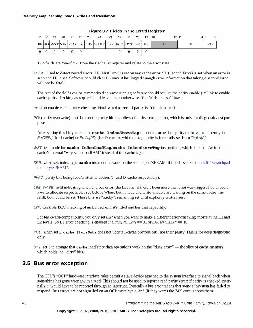
Memory map, caching, reads, writes and translation
43 Programming the MIPS32® 74K™ Core Family, Revision 02.14
Copyright © 2007, 2008, 2010, 2011 MIPS Technologies Inc. All rights reserved.
Figure 3.7 Fields in the ErrCtl Register
Two fields are ‘overflow’ from the CacheErr register and relate to the error state:
FE/SE: Used to detect nested errors. FE (FirstError) is set on any cache error. SE (Second Error) is set when an error isseen and FE is set. Software should clear FE once it has logged enough error information that taking a second errorwill not be fatal.
The rest of the fields can be summarized as such: running software should set just the parity enable (PE) bit to enablecache parity checking as required, and leave it zero otherwise. The fields are as follows:
PE: 1 to enable cache parity checking. Hard-wired to zero if parity isn’t implemented.
PO: (parity overwrite) - set 1 to set the parity bit regardless of parity computation, which is only for diagnostic/test pur-poses.
After setting this bit you can use cache IndexStoreTag to set the cache data parity to the value currently inErrCtl[PI] (for I-cache) or ErrCtl[PD] (for D-cache), while the tag parity is forcefully set from TagLo[P].
WST: test mode for cache IndexLoadTag/cache IndexStoreTag instructions, which then read/write thecache’s internal "way-selection RAM" instead of the cache tags.
SPR: when set, index-type cache instructions work on the scratchpad/SPRAM, if fitted - see Section 3.6, "Scratchpadmemory/SPRAM".
PI/PD: parity bits being read/written to caches (I- and D-cache respectively).
LBE, WABE: field indicating whether a bus error (the last one, if there’s been more than one) was triggered by a load ora write-allocate respectively: see below. Where both a load and write-allocate are waiting on the same cache-linerefill, both could be set. These bits are “sticky”, remaining set until explicitly written zero.
L2P: Controls ECC checking of an L2 cache, if it's fitted and has that capability.
For backward-compatibility, you only set L2P when you want to make a different error-checking choice at the L1 andL2 levels. So L2 error checking is enabled if ErrCtl[PE,L2P] == 01 or ErrCtl[PE,L2P] == 10.
PCD: when set 1, cache StoreData does not update I-cache precode bits, nor their parity. This is for deep diagnosticonly.
DYT: set 1 to arrange that cache load/store data operations work on the “dirty array” — the slice of cache memorywhich holds the “dirty” bits.
3.5 Bus error exception
The CPU’s “OCP” hardware interface rules permit a slave device attached to the system interface to signal back whensomething has gone wrong with a read. This should not be used to report a read parity error; if parity is checked exter-nally, it would have to be reported through an interrupt. Typically a bus error means that some subsystem has failed torespond. Bus errors are not signalled on an OCP write cycle, and (if they were) the 74K core ignores them.
31 30 29 28 27 26 25 24 23 22 21 20 19 18 12 11 4 3 0
PE PO WST SPR PCO ITC LBE WABE L2P PCD DYT SE FE 0 PI PD
0 0 0 0 0 0 0 0 0 0
3.6 Scratchpad memory/SPRAM
Programming the MIPS32® 74K™ Core Family, Revision 02.14 44
Copyright © 2007, 2008, 2010, 2011 MIPS Technologies Inc. All rights reserved.
Instruction bus error exceptions are precise (when the exception happens EPC always points to the instruction wherefetch failed). But a data-side bus error is usually caused by a load, and the (non-blocking) load which caused it mayhave happened a long time before the busy cycle finishes and the error is signalled. So a bus error exception caused bya load or store is imprecise; EPC does not necessarily (or even usually) point to the instruction causing the memoryread..
If software knows that a particular read might encounter a bus error - typically it’s some kind of probe - it should becareful to stall and wait for the load value immediately, by reading the value into a register, and make sure it can han-dle a bus error at that point.
There is an obscure corner case. The 74K core’s D-cache is “write-allocate”: so a write which misses in the cache willtrigger a read, to fill the cache line ready to receive the new data. If you’re unlucky enough to get a bus error on thatread-for-refill, the bus error will be associated with a store. After a bus error you can look at ErrCtl[LBE]/ErrCtl[WABE]to see whether the error was caused by a load or write-allocate.
3.6 Scratchpad memory/SPRAM
The 74K core (like most of MIPS Technologies’ cores) can be equipped with modestly-sized high speed on-chip datamemory, called scratchpad RAM or SPRAM. SPRAM is connected to a cache interface, alongside the I- and/or D-cache, so is available separately for the I- and D-side (ISPRAM and DSPRAM).
MIPS Technologies provide the interface on which users can build many types and sizes of SPRAM. We also providea “reference design” for both ISPRAM andDSPRAM, which is what is described here. If you keep the programminginterface the same as the reference design, you’re more likely to be able to find software support. The referencedesign allows for on-chip memories of up to 1Mbytes in size.
There are two possible motives for incorporating SPRAM:
• Dedicated high-speed memory: SPRAM runs with cache timing (multi-cycle SPRAM is supported for someother MIPS Technologies cores, but not on 74K cores).
SPRAM can be made larger than the maximum cache size.
Even for smaller sizes, it is possible to envisage applications where some particularly heavily-used piece of datais well-served by being permanently installed in SPRAM. Possible, but unusual. In most cases heavily-used datawill be handled well by the D-cache, and until you really know otherwise it’s better for the SoC designer to max-imize cache (compatible with his/her frequency needs.)
But there’s another more compelling use for a modest-size SPRAM:
• “DMA” accessible to external masters on the OCP interface: the SPRAM can be configured to be accessiblefrom an OCP interface. OCP masters will see it just as a chunk of memory which can be read or written.
Because SPRAM stands in for the cache, data passed through the SPRAM in this way doesn’t require any soft-ware cache management. This makes it spectacularly efficient as a staging area for communicating with complexI/O devices: a great way to implement “push” style I/O (that is where the device writes incoming data close to theCPU).
SPRAM must be located somewhere within the physical address map of the CPU, and is usually accessed throughsome “cached” region of memory (uncached region accesses to scratchpad work with the 74K reference design, butmay not do so on other implementations - better to access it through cacheable regions). It’s usually better to put it in
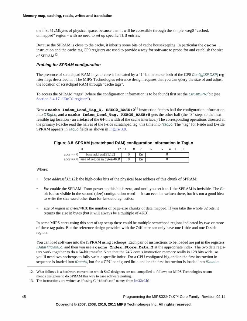
Memory map, caching, reads, writes and translation
45 Programming the MIPS32® 74K™ Core Family, Revision 02.14
Copyright © 2007, 2008, 2010, 2011 MIPS Technologies Inc. All rights reserved.
the first 512Mbytes of physical space, because then it will be accessible through the simple kseg0 “cached,unmapped” region - with no need to set up specific TLB entries.
Because the SPRAM is close to the cache, it inherits some bits of cache housekeeping. In particular the cacheinstruction and the cache tag CP0 registers are used to provide a way for software to probe for and establish the size
of SPRAM12.
Probing for SPRAM configuration
The presence of scratchpad RAM in your core is indicated by a “1” bit in one or both of the CP0 Config[ISP,DSP] reg-ister flags described in . The MIPS Technologies reference design requires that you can query the size of and adjustthe location of scratchpad RAM through “cache tags”.
To access the SPRAM “tags” (where the configuration information is to be found) first set the ErrCtl[SPR] bit (seeSection 3.4.17 “ErrCtl register”).
Now a cache Index_Load_Tag_D, KSEG0_BASE+013 instruction fetches half the configuration informationinto DTagLo, and a cache Index_Load_Tag, KSEG0_BASE+8 gets the other half (the “8” steps to the nextfeasible tag location - an artefact of the 64-bit width of the cache interface.) The corresponding operations directed atthe primary I-cache read the halves of the I-side scratchpad tag, this time into ITagLo. The “tag” for I-side and D-sideSPRAM appears in TagLo fields as shown in Figure 3.8.
Where:
• base address[31:12]: the high-order bits of the physical base address of this chunk of SPRAM;
• En: enable the SPRAM. From power-up this bit is zero, and until you set it to 1 the SPRAM is invisible. The Enbit is also visible in the second (size) configuration word — it can even be written there, but it’s not a good ideato write the size word other than for far-out diagnostics;
• size of region in bytes/4KB: the number of page-size chunks of data mapped. If you take the whole 32 bits, itreturns the size in bytes (but it will always be a multiple of 4KB).
In some MIPS cores using this sort of tag setup there could be multiple scratchpad regions indicated by two or moreof these tag pairs. But the reference design provided with the 74K core can only have one I-side and one D-sideregion.
You can load software into the ISPRAM using cacheops. Each pair of instructions to be loaded are put in the registersIDataHi/IDataLo, and then you use a cache Index_Store_Data_I at the appropriate index. The two data regis-ters work together to do a 64-bit transfer. Note that the 74K core’s instruction memory really is 128 bits wide, soyou’ll need two cacheops to fully write a specific index. For a CPU configured big-endian the first instruction insequence is loaded into IDataHi, but for a CPU configured little-endian the first instruction is loaded into IDataLo.
12. What follows is a hardware convention which SoC designers are not compelled to follow; but MIPS Technologies recom-mends designers to do SPRAM this way to ease software porting.
13. The instructions are written as if using C “#define” names from [m32c0.h]
Figure 3.8 SPRAM (scratchpad RAM) configuration information in TagLo31 12 11 8 7 6 5 4 1 0
addr == 0 base address[31:12] 0 En 0addr == 8 size of region in bytes/4KB 0 En 0
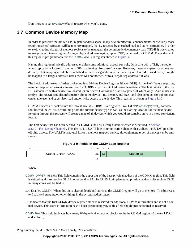
3.7 Common Device Memory Map
Programming the MIPS32® 74K™ Core Family, Revision 02.14 46
Copyright © 2007, 2008, 2010, 2011 MIPS Technologies Inc. All rights reserved.
Don’t forget to set ErrCtl[SPR] back to zero when you’re done.
3.7 Common Device Memory Map
In order to preserve the limited CP0 register address space, many new architectural enhancements, particularly thoserequiring several registers, will be memory mapped, that is, accessed by uncached load and store instructions. In orderto avoid creating dozens of memory regions to be managed, the common device memory map (CDMM) was createdto group them into one region. A single physical address region, up to 32KB, is defined for CDMM. The address ofthis region is programmable via the CDMMBase CP0 register shown in Figure 3-9.
Having this region physically addressed enables some additional access controls. On a core with a TLB, the regionwould typically be located in the first 256MB, allowing direct kseg1 access. However, if user or supervisor access wasdesired, TLB mappings could be established to map a useg address to the same region. On FMT based cores, it mightbe mapped to a kseg1 address if user access was not needed, or to a useg/kuseg address if it was.
The block of addresses is further broken up into 64-byte Device Register Blocks(DRB). A ‘device’ (feature requiringmemory mapped accesses), can use from 1-63 DRBs - up to 4KB of addressable registers. The first 64 bits of the firstDRB associated with a device is allocated for an Access Control and Status Register (of which only 32 are in use cur-rently). The ACSR provides information about the device - ID, version, and size - and also contains control bits thatcan enable user and supervisor read and/or write access to the device. This register is shown in Figure 3.10
CDMM devices are packed into the lowest available DRBs. Starting with 0 (or 1 if CDMMBase[CI] ==1), softwareshould read the ACSR, determining both the current device type as well as the starting location for the next device.Iterating through this process will create a map of all devices which you would presumably store in a more convienentformat.
The first device that has been defined in CDMM is the Fast Debug Channel which is described in Section8.1.10 “Fast Debug Channel”. This device is a UART-like communication channel that utilizes the EJTAG pins foroff-chip access. The UART is a natural fit for a memory mapped device, although many types of devices can be envi-sioned.
Figure 3-9 Fields in the CDMMBase Register
Where:
CDMM_UPPER_ADDR:: This field contains the upper bits of the base physical address of the CDMM region. This fieldis shifted by 4b, so that bits 31..11 correspond to PA bits 35..15. Unimplemented physical address bits such as 35..32in many cores will be tied to 0.
EN: Enables CDMM. When this bit is cleared, loads and stores to the CDMM region will go to memory. This bit resetsto 0 to avoid stepping on other things in the system address map.
CI: Indicates that the first 64-byte device register block is reserved for additional CDMM information and is not a nor-mal device. This extra information hasn’t been dreamed up yet, so this field should just be treated as reserved.
CDMMSize: This field indicates how many 64-byte device register blocks are in the CDMM region. (0 means 1 DRBand so forth)
31 11 10 9 8 0
CDMM_UPPER_ADDR EN CI CDMMSize
0
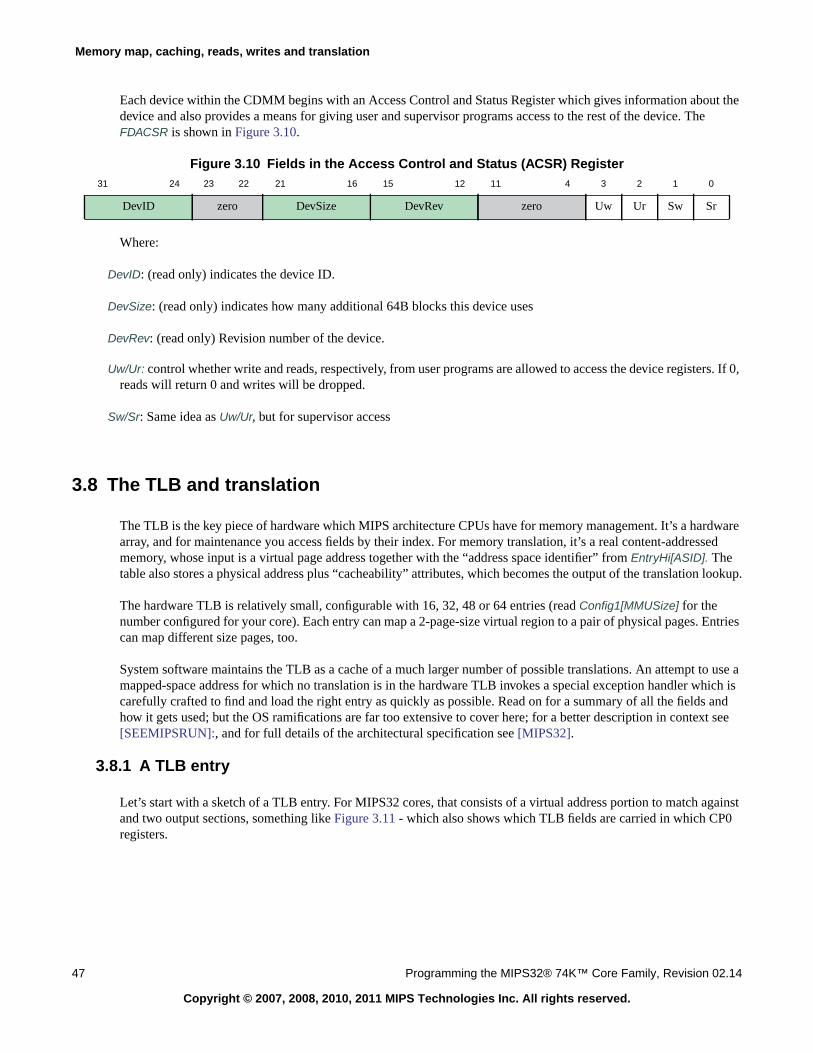
Memory map, caching, reads, writes and translation
47 Programming the MIPS32® 74K™ Core Family, Revision 02.14
Copyright © 2007, 2008, 2010, 2011 MIPS Technologies Inc. All rights reserved.
Each device within the CDMM begins with an Access Control and Status Register which gives information about thedevice and also provides a means for giving user and supervisor programs access to the rest of the device. TheFDACSR is shown in Figure 3.10.
Figure 3.10 Fields in the Access Control and Status (ACSR) Register
Where:
DevID: (read only) indicates the device ID.
DevSize: (read only) indicates how many additional 64B blocks this device uses
DevRev: (read only) Revision number of the device.
Uw/Ur: control whether write and reads, respectively, from user programs are allowed to access the device registers. If 0,reads will return 0 and writes will be dropped.
Sw/Sr: Same idea as Uw/Ur, but for supervisor access
3.8 The TLB and translation
The TLB is the key piece of hardware which MIPS architecture CPUs have for memory management. It’s a hardwarearray, and for maintenance you access fields by their index. For memory translation, it’s a real content-addressedmemory, whose input is a virtual page address together with the “address space identifier” from EntryHi[ASID]. Thetable also stores a physical address plus “cacheability” attributes, which becomes the output of the translation lookup.
The hardware TLB is relatively small, configurable with 16, 32, 48 or 64 entries (read Config1[MMUSize] for thenumber configured for your core). Each entry can map a 2-page-size virtual region to a pair of physical pages. Entriescan map different size pages, too.
System software maintains the TLB as a cache of a much larger number of possible translations. An attempt to use amapped-space address for which no translation is in the hardware TLB invokes a special exception handler which iscarefully crafted to find and load the right entry as quickly as possible. Read on for a summary of all the fields andhow it gets used; but the OS ramifications are far too extensive to cover here; for a better description in context see[SEEMIPSRUN]:, and for full details of the architectural specification see [MIPS32].
3.8.1 A TLB entry
Let’s start with a sketch of a TLB entry. For MIPS32 cores, that consists of a virtual address portion to match againstand two output sections, something like Figure 3.11 - which also shows which TLB fields are carried in which CP0registers.
31 24 23 22 21 16 15 12 11 4 3 2 1 0
DevID zero DevSize DevRev zero Uw Ur Sw Sr
3.8 The TLB and translation
Programming the MIPS32® 74K™ Core Family, Revision 02.14 48
Copyright © 2007, 2008, 2010, 2011 MIPS Technologies Inc. All rights reserved.
Some points to make about the TLB entry:
• The input-side virtual address fields (to the left) have the fields necessary to match an incoming address againstthis entry. “VPN” is (by OS tradition) a “virtual page number” - the high bits of the program (virtual) address.
“VPN2” is used to remind you that this address is for a double-page-size virtual region which will map to a pairof physical pages...
• The right-hand side (physical) fields are the information used to output a translation. There are a pair of outputsfor each input-match, and which of them is used is determined by the highest within-match address bit. So instandard form (when we’re using 4Kbyte pages) each entry translates an 8Kbyte region of virtual address, but wecan map each 4Kbyte page onto any physical address (with any permission flag bits).
• The size of the input region is configurable because the “PageMask” determines how many incoming address bitsto match. The 74K core allows page sizes of 4Kbytes, 16Kbytes and going on in powers of 4 up to 256Mbytes.That’s expressed by the legal values of PageMask, shown below.
• The “ASID” field extends the virtual address with an 8-bit, OS-assigned memory-space identifier so that transla-tions for multiple different applications can co-exist in the TLB (in Linux, for example, each application has dif-ferent code and data lying in the same virtual address region).
• The “G” (global) bit is not quite sure whether it’s on the input or output side - there’s only one, but it can be readand written through either of EntryLo0-1. When set, it causes addresses to match regardless of their ASID value,thus defining a part of the address space which will be shared by all applications. For example, Linux applica-tions share some “kseg2” space used for kernel extensions.
3.8.2 Live translation and micro-TLBs
When you’re really tuning out the last cycle, you need to know that in the 74K core the I-side translation is done by alittle table local to the instruction fetch unit, and called the ITLB (sometimes “micro-TLB” or “uTLB”). There areonly 4 entries in the ITLB, and it is functionally invisible to software: it’s automatically refilled from the main TLB(in this context it’s often called the joint TLB or JTLB) when required, and automatically cleared whenever the TLB isupdated. It costs six extra clocks to refill the ITLB for any access whose translation is not already present. In 74Kfamily cores (unlike other cores from MIPS Technologies) there is no D-side micro-TLB — D-side translation usesthe main TLB directly. uTLB entries can only map 4KB and 16KB pages (main TLB entries can handle a wholerange of sizes from 4KB to 256MB). When the uTLB is reloaded a translation marked for a size other than 4KB or16KB is down-converted as required.
3.8.3 Reading and writing TLB entries: Index, Random and Wired
Two CP0 registers work as simple indexes into the TLB array for programming: Index and Random. The oddly-named Wired controls Random’s behavior.
Figure 3.11 Fields in a 74K™ core TLB entryEntryHi EntryHi
VPN2 PageMask ASID G PFNFlags
PFNFlags
C D V C D V
PageMask EntryLo1 EntryLo0
Memory map, caching, reads, writes and translation
49 Programming the MIPS32® 74K™ Core Family, Revision 02.14
Copyright © 2007, 2008, 2010, 2011 MIPS Technologies Inc. All rights reserved.
Of these: Index determines which TLB entry is accessed by tlbwi. It’s also used for the result of a tlbp (theinstruction you use to see whether a particular address would be successfully translated by the CPU). Index onlyimplements enough bits to index the TLB, however big that is; but a tlbp which fails to find a match for the speci-fied virtual address sets bit 31 of Index (it’s easy to test for).
Random is implemented as a full CPU clock-rate downcounter. It won’t decrement below the value of Wired (when itgets there it bounces off and starts again at the highest legal index). In practice, when used inside the TLB refillexception handler, it delivers a random index into the TLB somewhere between the value of Wired and the top.Wired can therefore be set to reserve some TLB entries from random replacement - a good place for an OS to keeptranslations which must never cause a TLB translation-not-present exception.Previously, a tlbwr instruction wouldsimply write to the TLB entry that the Random register currently indicated. The core has been enhanced with a fea-ture (whose presence is indicated by Config6NMRUP = 1) to put a little more brains behind selecting a TLB entry to bereplaced. A table of the most recently used TLB entries is maintained and the core attempts to avoid selecting one ofthose. This avoids replacing often used pages and has been shown to reduce the number of TLB misses in most cases.Certain workloads, particularly those accessing data sequentially where the working set just exceeds the mappablecapacity of the non-wired TLB entries, may benefit from having a more random replacement where you sometimesget lucky and find a long unused page not yet replaced. For those applications, this function can be disabled by settingConfig6NMRUD = 1, but you are probably better off leaving it alone.
3.8.4 Reading and writing TLB entries - EntryLo0-1, EntryHi and PageMask registers
The TLB is accessed through staging registers which between them represent all the fields in each TLB entry; they’recalled EntryHi, PageMask and EntryLo0-1. The fields from EntryHi and PageMask are shown in Figure 3.12.
All these fields act as staging posts for entries being written to or read from the TLB. But some of them are moremagic than that...
EntryHi[VPN2]: is the page-pair address to be matched by the entry this reads/writes - see above.
However, on a TLB-related exception VPN2 is automagically set to the virtual address we were trying to translatewhen we got the exception. If - as is most often the case - the outcome of the exception handler is to find and install atranslation to that address, VPN2 (and generally the whole of EntryHi) will turn out to already have the right values init.
EntryHi[ASID]: does double-duty. It is used to stage data to and from the TLB, but in normal running software it’s alsothe source of the current "ASID" value, used to extend the virtual address to make sure you only get translations forthe current process.
Figure 3.12 Fields in the EntryHi and PageMask registers31 29 28 13 12 8 7 0
EntryHi VPN2 0 ASID
PageMask 0 Mask 0
3.8 The TLB and translation
Programming the MIPS32® 74K™ Core Family, Revision 02.14 50
Copyright © 2007, 2008, 2010, 2011 MIPS Technologies Inc. All rights reserved.
PageMask[Mask]: acts as a kind of backward mask, in that a 1 bit means "don’t compare this address bit when matchingthis address". However, only a restricted range of PageMask values are legal (that’s with "1"s filling thePageMask[Mask] field from low bits upward, two at a time):
Note that the uTLBs handle only 4Kbyte and 16Kbyte page sizes; other page sizes are down-converted to 4Kbyte or16Kbyte as they are referenced. For other page sizes this may cause an unexpectedly high rate of uTLB misses, whichcould be noticeable in unusual circumstances.
Then moving our attention to the output side, the two EntryLo0-1 are identical in format as shown in Figure 3.13.
In EntryLo0-1:
PFN: the "physical frame number" - traditional OS name for the high-order bits of the physical address. 24 bits of PFNtogether with 12 bits of in-page address make up a 36-bit physical address; but the 74K core has a 32-bit physicaladdress bus, and does not implement the four highest bits (which always read back as zero).
C: a code indicating how to cache data in this page - pages can be marked uncacheable and various flavours of cache-able. The codes here are shared with those used in CP0 registers for the cacheability of fixed address regions: seeTable 3.3 in Section 3.4.2, "Cacheability options" on page 33 .
D: the "dirty" flag. In hardware terms it’s just a write-enable (when it’s 0 you can’t do a store using addresses translatedhere, you’ll get an exception instead). However, software can use it to track pages which have been written to; whenyou first map a page you leave this bit clear, and then a first write causes an exception which you note somewhere inthe OS’ memory management tables (and of course remember to set the bit).
V: the "valid" flag. You’d think it doesn’t make much sense - why load an entry if it’s not valid? But this is very helpfulso you can make just one of a pair of pages valid.
G: the "global" bit. This really belongs to the input side, and there aren’t really two independent values for it. So youshould always make sure you set EntryLo0[G] and EntryLo1[G} the same.
3.8.5 TLB initialization and duplicate entries
TLB entries come up to random values on power-up, and must be initialized by hardware before use. Generally, earlybootstrap software should go through setting each entry to a harmless “invalid” value.
Since the TLB is a fully-associative array and entries are written by index, it’s possible to load duplicate entries - twoor more entries which match the same virtual address/ASID. In older MIPS CPUs it was essential to avoid duplicateentries - even duplicate entries where all the entries are marked “invalid”. Some designs could even suffer hardware
PageMask Size of each output page PageMask Size of each output page0x0000.0000 4Kbytes 0x007F.E000 4Mbytes0x0000.6000 16Kbytes 0x01FF.E000 16Mbytes0x0001.E000 64Kbytes 0x07FF.E000 64Mbytes0x0007.E000 256Kbytes 0x1FFF.E000 256Mbytes0x001F.E000 1Mbyte
Figure 3.13 Fields in the EntryLo0-1 registers31 30 29 6 5 3 2 1 0
0 PFN C D V G
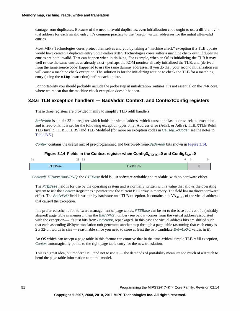
Memory map, caching, reads, writes and translation
51 Programming the MIPS32® 74K™ Core Family, Revision 02.14
Copyright © 2007, 2008, 2010, 2011 MIPS Technologies Inc. All rights reserved.
damage from duplicates. Because of the need to avoid duplicates, even initialization code ought to use a different vir-tual address for each invalid entry; it’s common practice to use “kseg0” virtual addresses for the initial all-invalidentries.
Most MIPS Technologies cores protect themselves and you by taking a “machine check” exception if a TLB updatewould have created a duplicate entry Some earlier MIPS Technologies cores suffer a machine check even if duplicateentries are both invalid. That can happen when initializing. For example, when an OS is initializing the TLB it maywell re-use the same entries as already exist - perhaps the ROM monitor already initialized the TLB, and (derivedfrom the same source code) happened to use the same dummy addresses. If you do that, your second initialization runwill cause a machine check exception. The solution is for the initializing routine to check the TLB for a matchingentry (using the tlbp instruction) before each update.
For portability you should probably include the probe step in initialization routines: it’s not essential on the 74K core,where we repeat that the machine check exception doesn’t happen.
3.8.6 TLB exception handlers — BadVaddr, Context, and ContextConfig registers
These three registers are provided mainly to simplify TLB refill handlers.
BadVAddr is a plain 32-bit register which holds the virtual address which caused the last address-related exception,and is read-only. It is set for the following exception types only: Address error (AdEL or AdES), TLB/XTLB Refill,TLB Invalid (TLBL, TLBS) and TLB Modified (for more on exception codes in Cause[ExcCode], see the notes toTable B.5.)
Context contains the useful mix of pre-programmed and borrowed-from-BadVAddr bits shown in Figure 3.14.
Figure 3.14 Fields in the Context register when Config3CTXTC=0 and Config3SM=0
Context[PTEBase,BadVPN2]: the PTEBase field is just software-writable and readable, with no hardware effect.
The PTEBase field is for use by the operating system and is normally written with a value that allows the operatingsystem to use the Context Register as a pointer into the current PTE array in memory. The field has no direct hardwareeffect. The BadVPN2 field is written by hardware on a TLB exception. It contains bits VA31..13 of the virtual addressthat caused the exception.
In a preferred scheme for software management of page tables, PTEBase can be set to the base address of a (suitablyaligned) page table in memory; then the BadVPN2 number (see below) comes from the virtual address associatedwith the exception—-it’s just bits from BadVAddr, repackaged. In this case the virtual address bits are shifted suchthat each ascending 8Kbyte translation unit generates another step through a page table (assuming that each entry is2 x 32-bit words in size — reasonable since you need to store at least the two candidate EntryLo0-1 values in it).
An OS which can accept a page table in this format can contrive that in the time-critical simple TLB refill exception,Context automagically points to the right page table entry for the new translation.
This is a great idea, but modern OS’ tend not to use it — the demands of portability mean it’s too much of a stretch tobend the page table information to fit this model.
31 23 22 4 3 0
PTEBase BadVPN2 0
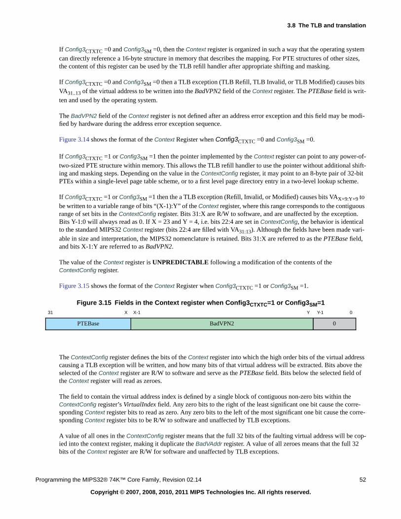
3.8 The TLB and translation
Programming the MIPS32® 74K™ Core Family, Revision 02.14 52
Copyright © 2007, 2008, 2010, 2011 MIPS Technologies Inc. All rights reserved.
If Config3CTXTC =0 and Config3SM =0, then the Context register is organized in such a way that the operating systemcan directly reference a 16-byte structure in memory that describes the mapping. For PTE structures of other sizes,the content of this register can be used by the TLB refill handler after appropriate shifting and masking.
If Config3CTXTC =0 and Config3SM =0 then a TLB exception (TLB Refill, TLB Invalid, or TLB Modified) causes bitsVA31..13 of the virtual address to be written into the BadVPN2 field of the Context register. The PTEBase field is writ-ten and used by the operating system.
The BadVPN2 field of the Context register is not defined after an address error exception and this field may be modi-fied by hardware during the address error exception sequence.
Figure 3.14 shows the format of the Context Register when Config3CTXTC =0 and Config3SM =0.
If Config3CTXTC =1 or Config3SM =1 then the pointer implemented by the Context register can point to any power-of-two-sized PTE structure within memory. This allows the TLB refill handler to use the pointer without additional shift-ing and masking steps. Depending on the value in the ContextConfig register, it may point to an 8-byte pair of 32-bitPTEs within a single-level page table scheme, or to a first level page directory entry in a two-level lookup scheme.
If Config3CTXTC =1 or Config3SM =1 then the a TLB exception (Refill, Invalid, or Modified) causes bits VAX+9:Y+9 tobe written to a variable range of bits “(X-1):Y” of the Context register, where this range corresponds to the contiguousrange of set bits in the ContextConfig register. Bits 31:X are R/W to software, and are unaffected by the exception.Bits Y-1:0 will always read as 0. If X = 23 and Y = 4, i.e. bits 22:4 are set in ContextConfig, the behavior is identicalto the standard MIPS32 Context register (bits 22:4 are filled with VA31:13). Although the fields have been made vari-able in size and interpretation, the MIPS32 nomenclature is retained. Bits 31:X are referred to as the PTEBase field,and bits X-1:Y are referred to as BadVPN2.
The value of the Context register is UNPREDICTABLE following a modification of the contents of theContextConfig register.
Figure 3.15 shows the format of the Context Register when Config3CTXTC =1 or Config3SM =1.
Figure 3.15 Fields in the Context register when Config3CTXTC=1 or Config3SM=1
The ContextConfig register defines the bits of the Context register into which the high order bits of the virtual addresscausing a TLB exception will be written, and how many bits of that virtual address will be extracted. Bits above theselected of the Context register are R/W to software and serve as the PTEBase field. Bits below the selected field ofthe Context register will read as zeroes.
The field to contain the virtual address index is defined by a single block of contiguous non-zero bits within theContextConfig register’s VirtualIndex field. Any zero bits to the right of the least significant one bit cause the corre-sponding Context register bits to read as zero. Any zero bits to the left of the most significant one bit cause the corre-sponding Context register bits to be R/W to software and unaffected by TLB exceptions.
A value of all ones in the ContextConfig register means that the full 32 bits of the faulting virtual address will be cop-ied into the context register, making it duplicate the BadVAddr register. A value of all zeroes means that the full 32bits of the Context register are R/W for software and unaffected by TLB exceptions.
31 X X-1 Y Y-1 0
PTEBase BadVPN2 0
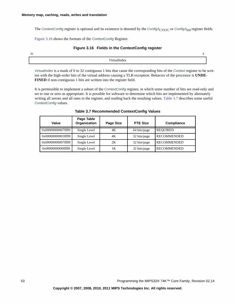
Memory map, caching, reads, writes and translation
53 Programming the MIPS32® 74K™ Core Family, Revision 02.14
Copyright © 2007, 2008, 2010, 2011 MIPS Technologies Inc. All rights reserved.
The ContextConfig register is optional and its existence is denoted by the Config3CTXTC or Config3SM register fields.
Figure 3.16 shows the formats of the ContextConfig Register.
Figure 3.16 Fields in the ContextConfig register
VirtualIndex is a mask of 0 to 32 contiguous 1 bits that cause the corresponding bits of the Context register to be writ-ten with the high-order bits of the virtual address causing a TLB exception. Behavior of the processor is UNDE-FINED if non-contiguous 1 bits are written into the register field.
It is permissible to implement a subset of the ContextConfig register, in which some number of bits are read-only andset to one or zero as appropriate. It is possible for software to determine which bits are implemented by alternatelywriting all zeroes and all ones to the register, and reading back the resulting values. Table 3.7 describes some usefulContextConfig values.
31 0
VirtualIndex
Table 3.7 Recommended ContextConfig Values
ValuePage Table
Organization Page Size PTE Size Compliance
0x00000000007ffff0 Single Level 4K 64 bits/page REQUIRED
0x00000000003ffff8 Single Level 4K 32 bits/page RECOMMENDED
0x00000000007ffff8 Single Level 2K 32 bits/page RECOMMENDED
0x0000000000fffff8 Single Level 1K 32 bits/page RECOMMENDED
3.8 The TLB and translation
Programming the MIPS32® 74K™ Core Family, Revision 02.14 54
Copyright © 2007, 2008, 2010, 2011 MIPS Technologies Inc. All rights reserved.
Chapter 4
Programming the MIPS32® 74K™ Core Family, Revision 02.14 55
Copyright © 2007, 2008, 2010, 2011 MIPS Technologies Inc. All rights reserved.
Programming the 74K™ core in user mode
This chapter is not very long, because in user mode one MIPS32-compliant CPU looks much like another. But noteverything — sections include:
• Section 4.1, "User-mode accessible “Hardware registers”"
• Section 4.2, "Prefetching data": how it works.
• Section 4.3, "Using “synci” when writing instructions": writing instructions without needing to use privilegedcache management instructions.
• Section 4.4, "The multiplier": multiply, multiply/accumulate and divide timings.
• Section 4.5, "Tuning software for the 74K‘ family pipeline": for determined programmers, and for compiler writ-ers. It includes information about the timing of the DSP ASE instructions.
• Section 4.6 “Tuning floating-point”: the floating-point unit often runs at half speed, and some of its interactions(particularly about potential exceptions) are complicated. This section offers some guidance about the timingissues you’ll encounter.
4.1 User-mode accessible “Hardware registers”
The 74K core complies with Revision 2 of the MIPS32 specification, which introduces hardware registers; CPU-dependent registers which are readable by unprivileged user space programs, usually to share information which isworth making accessible to programs without the overhead of a system call.
The hardware registers provide useful information about the hardware, even to unprivileged (user-mode) software,and are readable with the rdhwr instruction. [MIPS32] defines four registers so far. The OS can control access toeach register individually, through a bitmask in the CP0 register HWREna - (set bit 0 to enable register 0 etc).HWREna is cleared to all-zeroes on reset, so software has to explicitly enable user access — see Section 5.6 “TheHWREna register - Control user rdhwr access”. Privileged code can access any hardware register.
The five standard registers are:
• CPUNum (0): Number of the CPU on which the program is currently running. This comes directly from thecoprocessor 0 EBase[CPUNum] field.
• SYNCI_Step (1): the effective size of an L1 cache line14; this is now important to user programs because they cannow do things to the caches using the synci instruction to make instructions you’ve written visible for execu-tion. Then SYNCI_Step tells you the “step size” - the address increment between successive synci’s required tocover all the instructions in a range.
14. Strictly, it’s the lesser of the I-cache and D-cache line size, but it’s most unusual to make them different.
4.2 Prefetching data
Programming the MIPS32® 74K™ Core Family, Revision 02.14 56
Copyright © 2007, 2008, 2010, 2011 MIPS Technologies Inc. All rights reserved.
If SYNCI_Step returns zero, that means that your hardware ensures that your caches are instruction/data coher-ent, and you don’t need to use synci at all.
• CC (2): user-mode read-only access to the CP0 Count register, for high-resolution counting. Which wouldn’t bemuch good without.
• CCRes (3): which tells you how fast Count counts. It’s a divider from the pipeline clock — if the rdhwr instruc-tion reads a value of “2”, then Count increments every 2 cycles, at half the pipeline clock rate.For 74K familycores that is precisely what you will read.
• UL (30): user-mode read-only access to the CP0 UserLocal register. This register can be used to provide a threadidentifier to user-mode programs. See Section C.4.2 “The UserLocal register” for more details
4.2 Prefetching data
MIPS32 CPUs are being increasingly used for computations which feature loops accessing large arrays, and the run-time is often dominated by cache misses.
These are excellent candidates for using the pref instruction, which gets data into the cache without affecting theCPUs other state. In a well-optimized loop with prefetch, data for the next iteration can be fetched into the cache inparallel with computation for the last iteration.
It’s a pretty major principle that pref should have no software-visible effect other than to make things go faster.
pref is logically a no-op15.
The pref instruction comes with various possible “hints” which allow the program to express its best guess about thelikely fate of the cache line. In 74K family cores the “load” and “store” variants of the hints do the same thing; but itmakes good sense to use the hint which matches your program’s intention - you might one day port it to a CPU whereit makes a difference, and it can’t do any harm.
The 74K core acts on hints as summarized in Table 4.1.
4.3 Using “synci” when writing instructions
The synci instruction (introduced with Revision 2 of the MIPS32 architecture specification, [MIPS32]) ensures thatinstructions written by a program (necessarily through the D-cache, if you’re running cached) get written back fromthe D-cache and corresponding I-cache locations invalidated, so that any future execution at the address will reliablyexecute the new instructions. synci takes an address argument, and it takes effect on a whole enclosing cache-linesized piece of memory. User-level programs can discover the cache line size because it’s available in a “hardware reg-isters” accessed by rdhwr, as described in Section 4.1, "User-mode accessible “Hardware registers”" above.
Since synci is modifying the program’s own instruction stream, it’s inherently an “instruction hazard”: so whenyou’ve finished writing your instructions and issued the last synci, you should then use a jr.hb or equivalent to callthe new instructions — see Section 5.1 “Hazard barrier instructions”.
15. This isn’t quite true any more; pref with the “PrepareForStore” hint can zero out some data which wasn’t previously zero.
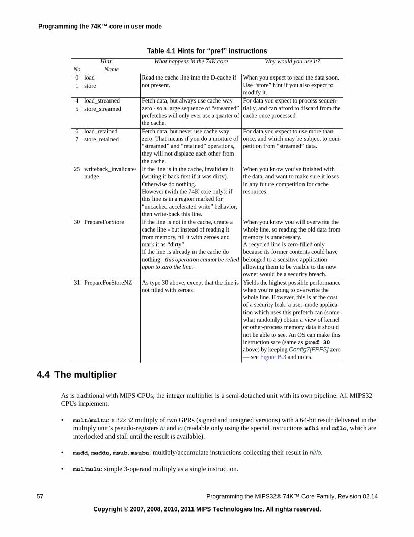
Programming the 74K™ core in user mode
57 Programming the MIPS32® 74K™ Core Family, Revision 02.14
Copyright © 2007, 2008, 2010, 2011 MIPS Technologies Inc. All rights reserved.
4.4 The multiplier
As is traditional with MIPS CPUs, the integer multiplier is a semi-detached unit with its own pipeline. All MIPS32CPUs implement:
• mult/multu: a 32×32 multiply of two GPRs (signed and unsigned versions) with a 64-bit result delivered in themultiply unit’s pseudo-registers hi and lo (readable only using the special instructions mfhi and mflo, which areinterlocked and stall until the result is available).
• madd, maddu, msub, msubu: multiply/accumulate instructions collecting their result in hi/lo.
• mul/mulu: simple 3-operand multiply as a single instruction.
Table 4.1 Hints for “pref” instructionsHint What happens in the 74K core Why would you use it?
No Name0 load Read the cache line into the D-cache if
not present.When you expect to read the data soon.Use “store” hint if you also expect tomodify it.
1 store
4 load_streamed Fetch data, but always use cache wayzero - so a large sequence of “streamed”prefetches will only ever use a quarter ofthe cache.
For data you expect to process sequen-tially, and can afford to discard from thecache once processed
5 store_streamed
6 load_retained Fetch data, but never use cache wayzero. That means if you do a mixture of“streamed” and “retained” operations,they will not displace each other fromthe cache.
For data you expect to use more thanonce, and which may be subject to com-petition from “streamed” data.
7 store_retained
25 writeback_invalidate/nudge
If the line is in the cache, invalidate it(writing it back first if it was dirty).Otherwise do nothing.However (with the 74K core only): ifthis line is in a region marked for“uncached accelerated write” behavior,then write-back this line.
When you know you’ve finished withthe data, and want to make sure it losesin any future competition for cacheresources.
30 PrepareForStore If the line is not in the cache, create acache line - but instead of reading itfrom memory, fill it with zeroes andmark it as “dirty”.If the line is already in the cache donothing - this operation cannot be reliedupon to zero the line.
When you know you will overwrite thewhole line, so reading the old data frommemory is unnecessary.A recycled line is zero-filled onlybecause its former contents could havebelonged to a sensitive application -allowing them to be visible to the newowner would be a security breach.
31 PrepareForStoreNZ As type 30 above, except that the line isnot filled with zeroes.
Yields the highest possible performancewhen you’re going to overwrite thewhole line. However, this is at the costof a security leak: a user-mode applica-tion which uses this prefetch can (some-what randomly) obtain a view of kernelor other-process memory data it shouldnot be able to see. An OS can make thisinstruction safe (same as pref 30above) by keeping Config7[FPFS] zero— see Figure B.3 and notes.
4.5 Tuning software for the 74K™ family pipeline
Programming the MIPS32® 74K™ Core Family, Revision 02.14 58
Copyright © 2007, 2008, 2010, 2011 MIPS Technologies Inc. All rights reserved.
• div/divu: divide - the quotient goes into lo and the remainder into hi.
Many of the most powerful instructions in the MIPS DSP ASE are variants of multiply or multiply-accumulate oper-ations, and are described in Chapter 9, “The MIPS32® DSP ASE” on page 121Chapter 7, “The MIPS32® DSP ASE”on page 87. The DSP ASE also provides three additional “accumulators” which behave like the hi/lo pair).
No multiply/divide operation ever produces an exception - even divide-by-zero is silent - so compilers typically insertexplicit check code where it’s required.
The 74K core multiplier is high performance and pipelined; multiply/accumulate instructions can run at a rate of 1per clock, but a 32×32 3-operand multiply takes six clocks longer than a simple ALU operation. Divides use a bit-per-clock algorithm, which is short-cut for smaller dividends. Multiply/divide instructions are generally slow enough thatit is difficult to arrange programs so that their results will be ready when needed.
4.5 Tuning software for the 74K™ family pipeline
This section is addressed to low-level programmers who are tuning software by hand and to those working on effi-cient compilers or code translators.
74K family cores have a complex out-of-order pipeline, which makes fine-grain instruction interactions very difficultto summarize. See Section 1.4 “A brief guide to the 74K‘ core implementation” for a reasonably accurate picture ofthe basic pipeline, from which you will be able to foresee some effects. We hope that a later version of this manualmay be able to be more helpful, but with a complex out-of-order CPU like this one you will always get more insightfrom running code on a real CPU or a cycle-accurate simulator.
4.5.1 Cache delays and mitigating their effect
In a typical 74K CPU implementation a cache miss which has to be refilled from DRAM memory (in the very nextchip on the board) will be delayed by a period of time long enough to run 50-200 instructions. A miss or uncachedread (perhaps of a device register) may easily be several times slower. These really are important!
Because these delays are so large, there’s not a lot you can do to help a cache-missing program make progress. Butevery little bit helps. The 74K core has non-blocking loads, so if you can move your load instruction producer awayfrom its consumer, you won’t start paying for your memory delay until you try to run the consuming instruction.
Compilers and programmers find it difficult to move fragments of algorithm backwards like this, so the architecturealso provides prefetch instructions (which fetch designated data into the D-cache, but do nothing else). Becausethey’re free of most side-effects it’s easier to issue prefetches very early. Any loop which walks predictably through alarge array is a candidate for prefetch instructions, which are conveniently placed within one iteration to prefetch datafor the next.
The pref PrepareForStore prefetch saves a cache refill read, for cache lines which you intend to overwrite intheir entirety. Read more about prefetch in Section 4.2, "Prefetching data" above.
Tuning data-intensive common functions
Bulk operations like bcopy() and bzero() will benefit from CPU-specific tuning. To get excellent performancefor in-cache data, it’s only necessary to reorganize the software enough to cover the address-to-store and load-to-usedelays. But to get the loop to achieve the best performance when cache missing, you probably want to use someprefetches. MIPS Technologies may have example code of such functions — ask.
Programming the 74K™ core in user mode
59 Programming the MIPS32® 74K™ Core Family, Revision 02.14
Copyright © 2007, 2008, 2010, 2011 MIPS Technologies Inc. All rights reserved.
4.5.2 Branch delay slot
It’s a feature of the MIPS architecture that it always attempts to execute the instruction immediately following abranch. The rationale for this is that it’s extremely difficult to fetch the branch target quickly enough to avoid a delay,so the extra instruction runs “for free”...
Most of the time, the compiler deals well with this single delay slot. MIPS low-level programmers find it odd at first,but you get used to it!
4.6 Tuning floating-point
It seemed to make more sense to put this information into the FPU chapter: read from Section 6.5 “FPU pipeline andinstruction timing”.
4.7 Branch misprediction delays
Programming the MIPS32® 74K™ Core Family, Revision 02.14 60
Copyright © 2007, 2008, 2010, 2011 MIPS Technologies Inc. All rights reserved.
4.7 Branch misprediction delays
In a long-pipeline design like this, branches would be expensive if you waited until the branch was executed beforefetching any more instructions. See Section 1.4 “A brief guide to the 74K‘ core implementation” for what is doneabout this: but the upshot is that where the fetch logic can’t compute the target address, or guesses wrong, that’s goingto cost 12 or more lost cycles (since when we’re not blocked on a cache miss we hope to average substantially morethan one instruction per clock, that’s worse than it sounds). It does depend what sort of branch: the conditional branchwhich closes a tight loop will almost always be predicted correctly after the first time around.
However, too many branches in too short a period of time can overwhelm the ability of the instruction fetch logic tokeep ahead with its predictions, even if the predictions are almost always right. Three empty cycles occur between thedelivery of the branch delay slot instruction and the first instruction(s) from the branch target location. Where branchycode can be replaced by conditional moves or tight loops “unrolled” a little to get at least 6-8 instructions betweenbranches, you’ll get significant benefits.
The branch-likely instructions deprecated by the MIPS32 architecture document are predicted just like any otherbranch. Misprediction of branch-likelies costs an extra cycle or two, because the branch and the delay slot instructionneeds to be re-executed after a mispredict. Branch-likely instructions sometimes improve the performance of smallloops on 74K family cores, but they set problems for the designers of complex CPUs, and may one day disappearfrom the standard. Good compilers for the MIPS32 architecture should provide an option to avoid these instructions.
4.8 Load delayed by (unrelated) recent store
Load instructions are handled within the execution unit (the AGEN pipeline) with “standard” timing, just so long asthey hit in the cache. When a load misses (or, handled the same way, turns out to be uncached) then a dependent oper-ation which has already been issued will have to be replayed if the dependent instruction has been dispatched. Thatgenerates long delays, but you already know about that. If the dependent instruction has not been dispatched at allthen it will wait in the DDQ until the load data becomes available.
However, store instructions are graduated before they are completed — which sounds problematic, but in fact youcan’t afford to let instructions write the cache (or commit a write to real memory) until they graduate and cease to bespeculative.
This presents a problem. A programmer may write code which stores a value in memory, then immediately loads thesame value. The CPU pipeline detects circumstances where instructions are dependent for register values, but cannotgo doing the same for addresses. The load can get the right data from an incomplete store as a side-effect of checkingwhether the data we want might be in the FSB (the “fill/store buffer”) attached to the D-cache: see Section3.3.1 “Read/write ordering and cache/memory data queues in the 74K‘ core” for more information. The store datacan also be in intermediate stages/queues before being written into the FSB. Any data that matches stores in suchintermediate queues will also be bypassed back to the pipeline as if the load hit in the cache.
4.9 Minimum load-miss penalty
74K family cores will typically run at high frequencies, so any load which misses in the L1 D-cache is likely to besubstantially delayed, waiting for the memory data to come back. However, if you ever use the core with a very fastmemory, it’s worth observing that even a fast-serviced miss is still a serious event. If an instruction which consumesthe loaded data issues before we’re sure the load missed (and most of the time the consumer will only be a few placesbehind in instruction sequence, and will have issued), then that instruction will have to be re-executed by stoppingexecution and starting again on the consuming instruction. That means it has to be re-fetched from the I-cache, andinvolves a delay of 15 cycles or so.
61 Programming the MIPS32® 74K™ Core Family, Revision 02.14
Copyright © 2007, 2008, 2010, 2011 MIPS Technologies Inc. All rights reserved.
4.10 Data dependency delays
The 74K core’s out-of-order pipeline does a very good job of running dependent instructions as soon as possible, inhardware. So to some extent it makes it unnecessary to manage data delays by moving instructions around in the pro-gram sequence (and if you feel you should try, it makes it tricky to predict the effect of your tuning). Ideally, youshould use an instrumented real CPU or cycle-accurate simulator to get insight into detailed tuning effects.
Compilers might reasonably try to schedule code to create more opportunities for dual-issue and so that instructionsmight be issued at full speed despite dependencies, but should rarely do so if the cost is significant — the hardware isalready gaining much of this advantage within its out-of-order window (think of it as looking 7-15 instructions aheadin the program sequence), and compiler scheduling will not be worth many extra instructions or significant code bloatunless it reaches beyond such a window. Loop unrolling will often help, but local scheduling will be unlikely to makea lot of difference.
We’ve attempted to tabulate all possible producer/consumer delays affecting user-level code (we’re not discussingCP0 registers here), but excluding floating point (which is in the next section). These are just fixed delays, of course:if a load misses in the cache, that’s different (and there are notes about it, above).
The MIPS instruction set is efficient for short pipelines because, most of the time, dependent instructions can be runnose-to-tail, just one clock apart, without extra delay. Even in the more sophisticated 74K family CPUs, most depen-dent instructions can run just two clocks apart. Each register has a “standard” place in the pipeline where the producershould deliver its value and another place in the pipeline where the consumer picks it up: where those places are 1cycle apart, the dependent instructions to run in successive cycles. Producer/consumer delays happen when either theproducer is late delivering a result to the register (a “lazy producer”), or the consumer insists on obtaining its operandearly (an “eager consumer”). If a lazy producer feeds an eager consumer, the delays add up.
Most of these delays are hidden by out-of-order execution. Moreover, non-dependent ALU and AGEN instructionsmay be issued simultaneously, so sometimes even a delay of zero cycles is painful.
Different register classes are read/written in different “standard” pipeline slots, so it’s important to be clear what classof registers is involved in any of these delays. For non-floating-point user-level code, there are just three:
• General purpose registers (“GPR”).
• The multiply unit’s hi/lo pair together with the three additional multiply-unit accumulators defined by the MIPSDSP ASE (“ACC”).
The MIPS architecture encourages implementations to provide integer multiply and divide operations in a sepa-rately-pipelined unit (see Section 4.4 “The multiplier”), and in 74K family cores this unit is capable of doingmultiply-accumulate operations at a rate of one per clock. No multiply unit operation ever causes an exception,which makes the longer multiply-unit pipeline rather invisible. It shows up in late delivery of GPR values bythose few multiply-unit instructions which deliver GPR results.
• The fields of the DSPControl register, used for condition codes and exceptional conditions resulting from DSPASE operations.
So that gives us two tables: Table 4.2 for our eager consumers, and Table 4.3 for the producers (we’ve listed even thenon-lazy producers, since there aren’t very many of them).
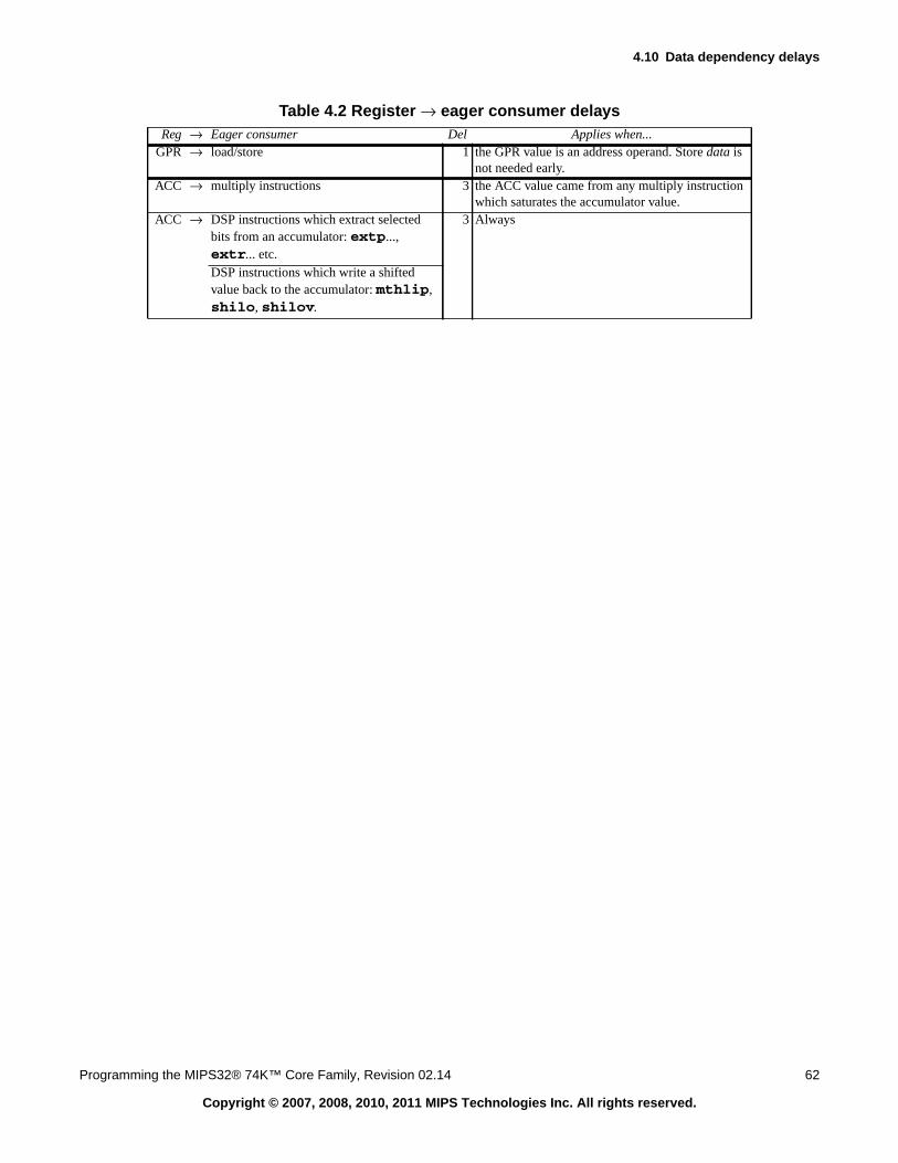
4.10 Data dependency delays
Programming the MIPS32® 74K™ Core Family, Revision 02.14 62
Copyright © 2007, 2008, 2010, 2011 MIPS Technologies Inc. All rights reserved.
Table 4.2 Register → eager consumer delaysReg → Eager consumer Del Applies when...
GPR → load/store 1 the GPR value is an address operand. Store data isnot needed early.
ACC → multiply instructions 3 the ACC value came from any multiply instructionwhich saturates the accumulator value.
ACC → DSP instructions which extract selectedbits from an accumulator: extp...,extr... etc.
3 Always
DSP instructions which write a shiftedvalue back to the accumulator: mthlip,shilo, shilov.
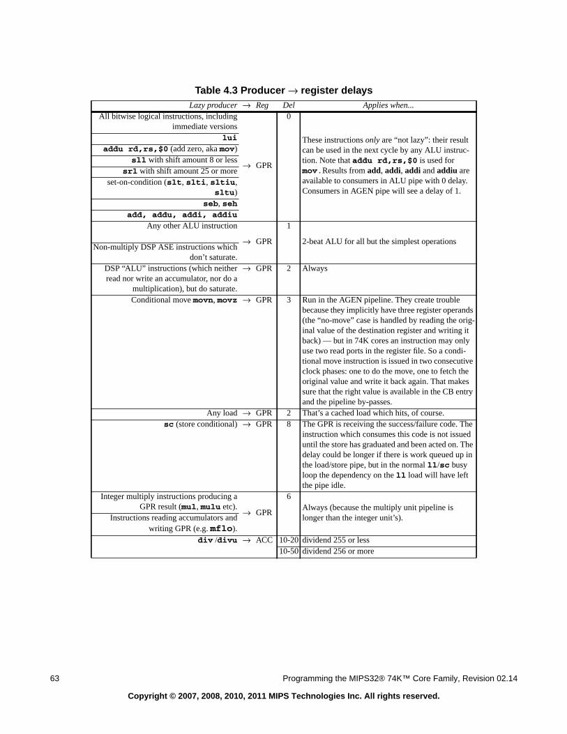
63 Programming the MIPS32® 74K™ Core Family, Revision 02.14
Copyright © 2007, 2008, 2010, 2011 MIPS Technologies Inc. All rights reserved.
Table 4.3 Producer → register delaysLazy producer → Reg Del Applies when...
All bitwise logical instructions, includingimmediate versions
→ GPR
0
These instructions only are “not lazy”: their resultcan be used in the next cycle by any ALU instruc-tion. Note that addu rd,rs,$0 is used formov.Results from add, addi, addi and addiu areavailable to consumers in ALU pipe with 0 delay.Consumers in AGEN pipe will see a delay of 1.
lui
addu rd,rs,$0 (add zero, aka mov)sll with shift amount 8 or less
srl with shift amount 25 or moreset-on-condition (slt, slti, sltiu,
sltu)seb, seh
add, addu, addi, addiu
Any other ALU instruction
→ GPR
1
2-beat ALU for all but the simplest operationsNon-multiply DSP ASE instructions which
don’t saturate.DSP “ALU” instructions (which neitherread nor write an accumulator, nor do a
multiplication), but do saturate.
→ GPR 2 Always
Conditional move movn, movz → GPR 3 Run in the AGEN pipeline. They create troublebecause they implicitly have three register operands(the “no-move” case is handled by reading the orig-inal value of the destination register and writing itback) — but in 74K cores an instruction may onlyuse two read ports in the register file. So a condi-tional move instruction is issued in two consecutiveclock phases: one to do the move, one to fetch theoriginal value and write it back again. That makessure that the right value is available in the CB entryand the pipeline by-passes.
Any load → GPR 2 That’s a cached load which hits, of course.sc (store conditional) → GPR 8 The GPR is receiving the success/failure code. The
instruction which consumes this code is not issueduntil the store has graduated and been acted on. Thedelay could be longer if there is work queued up inthe load/store pipe, but in the normal ll/sc busyloop the dependency on the ll load will have leftthe pipe idle.
Integer multiply instructions producing aGPR result (mul, mulu etc).
→ GPR
6Always (because the multiply unit pipeline islonger than the integer unit’s).Instructions reading accumulators and
writing GPR (e.g. mflo).div /divu → ACC 10-20 dividend 255 or less
10-50 dividend 256 or more
4.10 Data dependency delays
Programming the MIPS32® 74K™ Core Family, Revision 02.14 64
Copyright © 2007, 2008, 2010, 2011 MIPS Technologies Inc. All rights reserved.
How to use the tables
Suppose we’ve got an instruction sequence like this one:
addiu $a0, $a0, 8lw $t0, 0($a0) # [1]lw $t1, 4($a0)addu $t2, $t0, $t1# [2]mul $v0, $t2, $t3sw $v0, 0($a1) # [3]
Then a look at the tables should help us discover whether any instructions will be held up. Look at the dependencieswhere an instruction is dependent on its predecessor:
[1] The lw will be held up by two clocks. One clock because addiu takes 2 clocks to produce its result, and anotherbecause its GPR address operand $a0 was computed by the immediately preceding instruction (see the “load/storeaddress” box of Table 4.2.) The second lw will be OK.
[2] The addu will be two clocks late, because the load data from the preceding lw arrives late in the GPR $t1 (see the“load” box of Table 4.3.)
[3] The sw will be 6 clocks late starting while it waits for a result from the multiply pipe (the “multiply” box of Table4.3.)
These can be additive. In the pointer-chasing sequence:
lw $t1, 0($t0)lw $t2, 0($t1)
The second load will be held up three clocks: two because of the late delivery of load data in $t1 (“load” box ofTable 4.3), plus another because that data is required to form the address (“load/store address” box of Table 4.2.)
Delays caused by dependencies on DSPControl fields
Some DSP ASE instructions are dependent because they produce and consume values kept in fields of theDSPControl register. However, the most performance-critical of these dependencies are “by-passed” to make sure nodelay will occur - those are the dependencies between:
But other dependencies passed in DSPControl may cause delays; in particular the DSPControl[ouflag] bits set by vari-ous kinds of overflow are not ready for a succeeding rddsp instruction. The access is interlocked, and will lead to adelay of up to three clocks. We don’t expect that to be a problem (but if you know different, please get in touch withMIPS Technologies).
4.10.1 More complicated dependencies
There can be delays which are dependent on the dynamic allocation of resources inside the CPU. In general you can’treally figure out how much these matter by doing a static code analysis, and we earnestly advise you to get some kindof high-visibility cycle-accurate simulator or trace equipment.
addsc → DSPControl[c] → addwccmp.x → DSPControl[ccond] → pick.xwrdsp → DSPControl[pos,scount] → insv
65 Programming the MIPS32® 74K™ Core Family, Revision 02.14
Copyright © 2007, 2008, 2010, 2011 MIPS Technologies Inc. All rights reserved.
4.11 Advice on tuning instruction sequences (particularly DSP)
DSP algorithm functions are often the subject of intense tuning. There is some specific and helpful advice (withexamples) included in the white paper [DSPWP] published by MIPS Technologies.
But you need to know the basic latencies of instructions as executed by the 74K core (that is, how many cycles latercan a dependent instruction be issued). For these purposes there are four classes of instructions:
• A group of specially-simple ALU instructions run in one cycle. This includes bitwise logical instructions, mov(an alias for addu with $0), shifts up to 8 positions down or up, test-and-set instructions, and sign-extend instruc-tions. See the list at the top of Table 4.3.
• Simple DSP ASE operations (no multiply, no saturation) have 2-cycle latency, the same as most regular MIPS32arithmetic.
• Non-multiply DSP instructions which feature saturation or rounding have 3-cycle latency.
• Special DSP multiply operations (or any other access to the multiply unit accumulators): these have timings likestandard multiply and multiply-accumulate instructions, so they’re in with the multiply operations under the nextheading.
• Instruction dependencies relating to different fields in the DSPControl register are tracked separately, and effi-ciently, as if they were separate registers. But any rddsp or wrdsp instruction which reads/writes multiple fieldsat once is dependent on multiple fields, and that can’t be tracked through the CB system. Such a rddsp is notissued until all predecessors have graduated, and such a wrdsp must graduate before its successors can issue.You can often avoid this by using the “masked” versions of these instructions to read or write only the fieldyou’re particularly interested in.
4.12 Multiply/divide unit and timings
As is traditional with MIPS CPUs, the integer multiplier is a semi-detached unit with its own pipeline. All MIPS32CPUs implement:
• mult/multu: multiply two 32-bit numbers from GPRs (signed and unsigned versions) with a 64-bit result deliv-ered in the multiply unit’s accumulator. The accumulator was traditionally seen as pseudo-registers hi and lo,readable only using the special instructions mfhi and mflo.Operations into the accumulator do not hold up themain CPU and run independently, but mfhi/mflo are interlocked and delay execution as required until the resultis available.
• madd, maddu, msub, msubu: multiply/accumulate instructions collecting their result in the accumulator.
• mul/mulu: simple 3-operand multiply as a single instruction.
• div/divu: divide - the quotient goes into lo and the remainder into hi.
Many of the most powerful instructions in the MIPS DSP ASE are variants of multiply or multiply-accumulate oper-ations, and are described in Chapter 7, “The MIPS32® DSP ASE” on page 87. The DSP ASE also provides threeadditional “accumulators” which behave like the hi/lo pair: the now four accumulators are called ac0-3). When wetalk about the “multiply/divide” group of instructions we include any instruction which reads or writes any accumula-tor.
4.12 Multiply/divide unit and timings
Programming the MIPS32® 74K™ Core Family, Revision 02.14 66
Copyright © 2007, 2008, 2010, 2011 MIPS Technologies Inc. All rights reserved.
No multiply/divide operation ever produces an exception - even divide-by-zero is silent — compilers typically insertexplicit check code where it’s required.
Timing varies. Multiply-accumulate instructions (there are many different flavors of MAC in the DSP ASE) havebeen pipelined and tuned to achieve a 1-instruction-per-clock repeat rate, even for sequences of instructions targetingthe same accumulator. But because that requires a relatively long pipeline, multiply/divide unit instructions whichproduce a result in a GP register are relatively “slow”: for example, an instruction consuming the register value froma mflo will not be issued until at least 7 cycles after the mflo.
Divides are much slower again. All the timings are summarized in Table 4.3.
What that means is that in an instruction sequence like:
mult $1, $2mflo $3addu $2, $3, 1
The mflo will be issued 4 cycles after the mult, and the addu will go at least 2 cycles after the mflo. The executionunit may (or may not) be able to find other instructions to keep it busy, but each trip through that code sequence willtake a minimum of 9 cycles.
Chapter 5
Programming the MIPS32® 74K™ Core Family, Revision 02.14 67
Copyright © 2007, 2008, 2010, 2011 MIPS Technologies Inc. All rights reserved.
Kernel-mode (OS) programming and Release 2 of theMIPS32® Architecture
[MIPS32] tells you how to write OS code which is portable across all compliant CPUs. Most OS code should beCPU-independent, and we won’t tell you how to write it here. But release 2 of the MIPS32 Specification [MIPS32]introduced a few new optional features which are not yet well known, so are worth describing here:
• A better way of managing software-visible pipeline and hardware delays associated with CP0 programming inSection 5.1, "Hazard barrier instructions".
• New interrupt facilities described in Section 5.2, "MIPS32® Architecture Release 2 - enhanced interruptsystem(s)";
• That led on to Section 5.3.1 “Summary of exception entry points”: where do exceptions go, and what options areavailable?
• The ability to use one or more extra sets of registers (“shadow sets”) to reduce context-saving overhead in inter-rupt handlers, in Section 5.4, "Shadow registers".
• How to get at any power-saving features, in Section 5.5, "Saving Power"
• How to control user-privilege access to “hardware registers”, in Section 5.6 “The HWREna register - Controluser rdhwr access”.
5.1 Hazard barrier instructions
When privileged “CP0” instructions change the machine state, you can get unexpected behavior if an effect isdeferred out of its normal instruction sequence. But that can happen because the relevant control register only getswritten some way down the pipeline, or because the changes it makes are sensed by other instructions early in theirpipeline sequence: this is called a CP0 hazard.
Your 74K family core offers you the option of removing many CP0 hazards by setting the Config7[IHB] option bit asdescribed in the notes to Table B.3. But you might be better off sticking to the rules described in [MIPS32], so yourcode will run on any compliant CPU: it may be best to see this feature as the way to rescue legacy code.
It’s possible to get hazards in user mode code too, and many of the instructions described here are not solely for ker-nel-privilege code. But they’re most often met around CP0 read/writes, so they found their way to this chapter.
Traditionally, MIPS CPUs left the kernel/low-level software engineer with the job of designing sequences which areguaranteed to run correctly, usually by padding the dangerous operation with enough nop or ssnop instructions.
From Release 2 of the MIPS32 specification this is replaced by explicit hazard barrier instructions. If you execute ahazard barrier between the instruction which makes the change (the “producer”) and the instruction which is sensitiveto it (the “consumer”), you are guaranteed that the change will be seen as complete. Hazards can appear when the pro-
5.2 MIPS32® Architecture Release 2 - enhanced interrupt system(s)
Programming the MIPS32® 74K™ Core Family, Revision 02.14 68
Copyright © 2007, 2008, 2010, 2011 MIPS Technologies Inc. All rights reserved.
ducer affects even the instruction fetch of the consumer - that’s an “instruction hazard” - or only affecting the opera-tion of the consuming instruction (an “execution hazard”). Hazard barriers come in two strengths: ehb deals onlywith execution hazards, while eret, jr.hb and jalr.hb are barriers to both kinds of hazard.
In most implementations the strong hazard barrier instructions are quite costly, often discarding most or all of thepipeline contents: they should not be used indiscriminately. For efficiency you should use the weaker ehb where it isenough. Since some implementations work by holding up execution of all instructions after the barrier, it’s preferableto place the barrier just before the consumer, not just after the producer.
For example you might be updating a TLB entry:
mtc0 Index, t0# other stuff, if there’s stuff to doehbtlbwijr.hb ra
The ehb makes sure that the change to Index has been made before you attempt to write the TLB entry, which is fine.But updating the TLB might affect how instructions are fetched in mapped space, so you should not return to codewhich might be running in mapped space until you’ve cleared the “instruction hazard”. That’s dealt with by thejr.hb.
The unconditional hardware interlock between an mtco and an mfco instruction has been removed. An ehb instruc-tion is now required between an MTC0 and a MFC0 instruction type only when there is a CP0 register dependency.This optimization reduces the stall cycles incurred by software TLB refill exception handlers when accessing excep-tion and TLB-related state, The reduction in overhead of handling TLB refill exceptions has a significant impact onsystem performance. For more information, refer to the description of the sync instruction in the 74K™ SoftwareUser’s Manual .
Porting software to use the new instructions
If you know your software will only ever run on a MIPS32 Release 2 or higher CPU, then that’s great. But to maintainsoftware which has to continue running on older CPUs:
• ehb is a no-op: on all previous CPUs. So you can substitute an ehb for the last no-op in your sequence of“enough no-ops”, and your software is now safe on all future CPUs which are compliant with Release 2.
• jr.hb and jalr.hb: are decoded as plain jump-register and call-by-register instructions on earlier CPUs. Again, pro-vided you already had enough no-ops for your worst-case older CPU, your system should now be safe on Release2 and higher CPUs.
5.2 MIPS32® Architecture Release 2 - enhanced interrupt system(s)
The features for handling interrupts include:
• Vectored Interrupt (VI) mode offers multiple entry points (one for each of the interrupt sources), instead of thesingle general exception entry point.
External Interrupt Controller (EIC) mode goes further, and reinterprets the six core interrupt input signals as a64-value field - potentially 63 distinguished interrupts each with their own entry point (the zero code, of course,is reserved to mean “no interrupt active”).
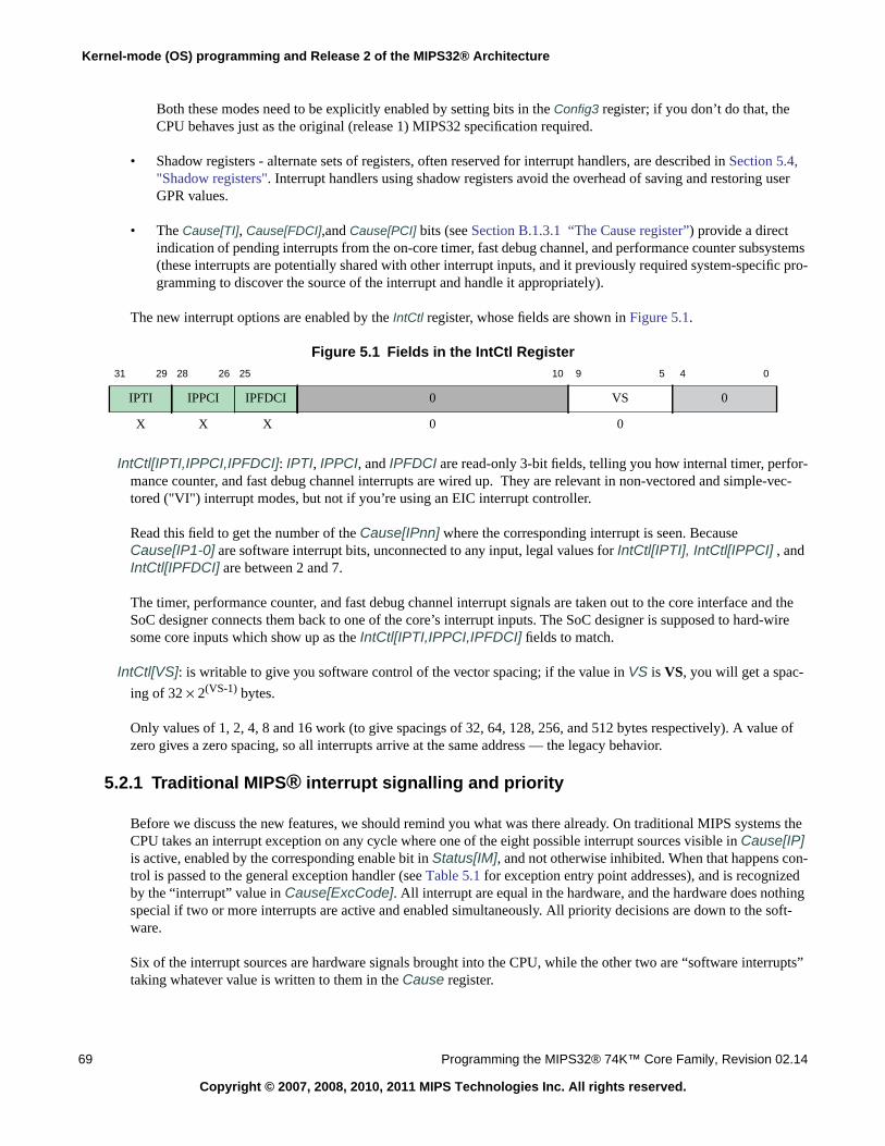
Kernel-mode (OS) programming and Release 2 of the MIPS32® Architecture
69 Programming the MIPS32® 74K™ Core Family, Revision 02.14
Copyright © 2007, 2008, 2010, 2011 MIPS Technologies Inc. All rights reserved.
Both these modes need to be explicitly enabled by setting bits in the Config3 register; if you don’t do that, theCPU behaves just as the original (release 1) MIPS32 specification required.
• Shadow registers - alternate sets of registers, often reserved for interrupt handlers, are described in Section 5.4,"Shadow registers". Interrupt handlers using shadow registers avoid the overhead of saving and restoring userGPR values.
• The Cause[TI], Cause[FDCI],and Cause[PCI] bits (see Section B.1.3.1 “The Cause register”) provide a directindication of pending interrupts from the on-core timer, fast debug channel, and performance counter subsystems(these interrupts are potentially shared with other interrupt inputs, and it previously required system-specific pro-gramming to discover the source of the interrupt and handle it appropriately).
The new interrupt options are enabled by the IntCtl register, whose fields are shown in Figure 5.1.
Figure 5.1 Fields in the IntCtl Register
IntCtl[IPTI,IPPCI,IPFDCI]: IPTI, IPPCI, and IPFDCI are read-only 3-bit fields, telling you how internal timer, perfor-mance counter, and fast debug channel interrupts are wired up. They are relevant in non-vectored and simple-vec-tored ("VI") interrupt modes, but not if you’re using an EIC interrupt controller.
Read this field to get the number of the Cause[IPnn] where the corresponding interrupt is seen. BecauseCause[IP1-0] are software interrupt bits, unconnected to any input, legal values for IntCtl[IPTI], IntCtl[IPPCI] , andIntCtl[IPFDCI] are between 2 and 7.
The timer, performance counter, and fast debug channel interrupt signals are taken out to the core interface and theSoC designer connects them back to one of the core’s interrupt inputs. The SoC designer is supposed to hard-wiresome core inputs which show up as the IntCtl[IPTI,IPPCI,IPFDCI] fields to match.
IntCtl[VS]: is writable to give you software control of the vector spacing; if the value in VS is VS, you will get a spac-
ing of 32 × 2(VS-1) bytes.
Only values of 1, 2, 4, 8 and 16 work (to give spacings of 32, 64, 128, 256, and 512 bytes respectively). A value ofzero gives a zero spacing, so all interrupts arrive at the same address — the legacy behavior.
5.2.1 Traditional MIPS® interrupt signalling and priority
Before we discuss the new features, we should remind you what was there already. On traditional MIPS systems theCPU takes an interrupt exception on any cycle where one of the eight possible interrupt sources visible in Cause[IP]is active, enabled by the corresponding enable bit in Status[IM], and not otherwise inhibited. When that happens con-trol is passed to the general exception handler (see Table 5.1 for exception entry point addresses), and is recognizedby the “interrupt” value in Cause[ExcCode]. All interrupt are equal in the hardware, and the hardware does nothingspecial if two or more interrupts are active and enabled simultaneously. All priority decisions are down to the soft-ware.
Six of the interrupt sources are hardware signals brought into the CPU, while the other two are “software interrupts”taking whatever value is written to them in the Cause register.
31 29 28 26 25 10 9 5 4 0
IPTI IPPCI IPFDCI 0 VS 0
X X X 0 0
5.2 MIPS32® Architecture Release 2 - enhanced interrupt system(s)
Programming the MIPS32® 74K™ Core Family, Revision 02.14 70
Copyright © 2007, 2008, 2010, 2011 MIPS Technologies Inc. All rights reserved.
The original MIPS32 specification adds an option to this. If you set the Cause[IV] bit, the same priority-blind inter-rupt handling happens but control is passed to an interrupt exception entry point which is separate from the generalexception handler.
5.2.2 VI mode - multiple entry points, interrupt signalling and priority
The traditional interrupt system fits with a RISC philosophy (it leaves all interrupt priority policy to software). It’salso OK with complex operating systems, which commonly have a single piece of code which does the housekeepingassociated with interrupts prior to calling an individual device-interrupt handler.
A single entry point doesn’t fit so well with embedded systems using very low-level interrupt handlers to performsmall near-the-hardware tasks. So Release 2 of the MIPS32 architecture adds “VI interrupt mode” where interruptsare despatched to one of eight possible entry points. To make this happen:
1. Config3[VInt] must be set, to indicate that your core has the vectored-interrupts feature - but all cores in the 74Kfamily have it;
2. You write Cause[IV] = 1 to request that interrupts use the special interrupt entry point; and:
3. You set IntCtl[VS] non-zero, setting the spacing between successive interrupt entry points.
Then interrupt exceptions will go to one of eight distinct entry points. The bit-number in Cause[IP] corresponding tothe highest-numbered active interrupt becomes the “vector number” in the range 0-7. The vector number is multipliedby the “spacing” implied by the OS-written field IntCtl[VS] (see above) to generate an offset. This offset is then addedto the special interrupt entry point (already an offset of 0x200 from the value defined in EBase) to produce the entrypoint to be used.
If multiple interrupts are active and enabled, the entry point will be the one associated with the higher-numberedinterrupt: in VI mode interrupts are no longer all equal, and the hardware now has some role in interrupt “priority”.
5.2.3 External Interrupt Controller (EIC) mode
Embedded systems have lots of interrupts, typically far exceeding the six input signals traditionally available. Mostsystems have an external interrupt controller to allow these interrupts to be masked and selected. If your interrupt con-troller is “EIC compatible” and you use these features, then you get 63 distinct interrupt entry points.
To do this the same six hardware signals used in traditional and VI modes are redefined as a bus with 64 possible val-
ues16: 0 means “no interrupt” and 1-63 represent distinct interrupts. That’s “EIC interrupt mode”, and you’re in EICmode if you would be in VI mode (see previous section) and additionally the Config3[VEIC] bit is set. EIC mode is alittle deceptive: the programming interface hardly seems to change, but the meaning of fields change quite a bit.
Firstly, once the interrupt bits are grouped the interrupt mask bits in Status[IM] can’t just be bitwise enables any more.Instead this field (strictly, the 6 high order bits of this field, excluding the mask bits for the software interrupts) isrecycled to become a 6-bit Status[IPL] (“interrupt priority level”) field. Most of the time (when running applicationcode, or even normal kernel code) Status[IPL] will be zero; the CPU takes an interrupt exception when the interruptcontroller presents a number higher than the current value of Status[IPL] on its “bus” and interrupts are not otherwiseinhibited.
16. The resulting system will be familiar to anyone who’s used a Motorola 68000 family device (or further back, a DEC PDP/11or any of its successors).
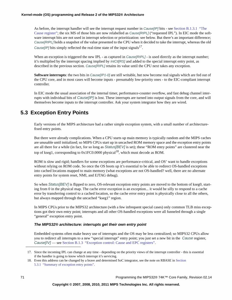
Kernel-mode (OS) programming and Release 2 of the MIPS32® Architecture
71 Programming the MIPS32® 74K™ Core Family, Revision 02.14
Copyright © 2007, 2008, 2010, 2011 MIPS Technologies Inc. All rights reserved.
As before, the interrupt handler will see the interrupt request number in Cause[IP] bits - see Section B.1.3.1 “TheCause register”; the six MS of those bits are now relabelled as Cause[RIPL] (“requested IPL”). In EIC mode the soft-ware interrupt bits are not used in interrupt selection or prioritization: see below. But there’s an important difference;Cause[RIPL] holds a snapshot of the value presented to the CPU when it decided to take the interrupt, whereas the old
Cause[IP] bits simply reflected the real-time state of the input signals17.
When an exception is triggered the new IPL - as captured in Cause[RIPL] - is used directly as the interrupt number;it’s multiplied by the interrupt spacing implied by IntCtl[RS] and added to the special interrupt entry point, asdescribed in the previous section. Cause[RIPL] retains its value until the CPU next takes any exception.
Software interrupts: the two bits in Cause[IP1-0] are still writable, but now become real signals which are fed out ofthe CPU core, and in most cases will become inputs - presumably low-priority ones - to the EIC-compliant interruptcontroller.
In EIC mode the usual association of the internal timer, performance-counter overflow, and fast debug channel inter-rupts with individual bits of Cause[IP] is lost. These interrupts are turned into output signals from the core, and willthemselves become inputs to the interrupt controller. Ask your system integrator how they are wired.
5.3 Exception Entry Points
Early versions of the MIPS architecture had a rather simple exception system, with a small number of architecture-fixed entry points.
But there were already complications. When a CPU starts up main memory is typically random and the MIPS cachesare unusable until initialized; so MIPS CPUs start up in uncached ROM memory space and the exception entry pointsare all there for a while (in fact, for so long as Status[BEV] is set); these “ROM entry points” are clustered near the
top of kseg1, corresponding to 0x1FC0.0000 physical18, which must decode as ROM.
ROM is slow and rigid; handlers for some exceptions are performance-critical, and OS’ want to handle exceptionswithout relying on ROM code. So once the OS boots up it’s essential to be able to redirect OS-handled exceptionsinto cached locations mapped to main memory (what exceptions are not OS-handled? well, there are no alternateentry points for system reset, NMI, and EJTAG debug).
So when Status[BEV] is flipped to zero, OS-relevant exception entry points are moved to the bottom of kseg0, start-ing from 0 in the physical map. The cache error exception is an exception... it would be silly to respond to a cacheerror by transferring control to a cached location, so the cache error entry point is physically close to all the others,but always mapped through the uncached “kseg1” region.
In MIPS CPUs prior to the MIPS32 architecture (with a few infrequent special cases) only common TLB miss excep-tions got their own entry point; interrupts and all other OS-handled exceptions were all funneled through a single“general” exception entry point.
The MIPS32® architecture: interrupts get their own entry point
Embedded systems often make heavy use of interrupts and the OS may be less centralized; so MIPS32 CPUs allowyou to redirect all interrupts to a new “special interrupt” entry point; you just set a new bit in the Cause register,Cause[IV] — see Section B.1.3 “Exception control: Cause and EPC registers”.
17. Since the incoming IPL can change at any time - depending on the priority views of the interrupt controller - this is essentialif the handler is going to know which interrupt it’s servicing.
18. Even this address can be changed by a brave and determined SoC integrator, see the note on RBASE in Section5.3.1 “Summary of exception entry points”.
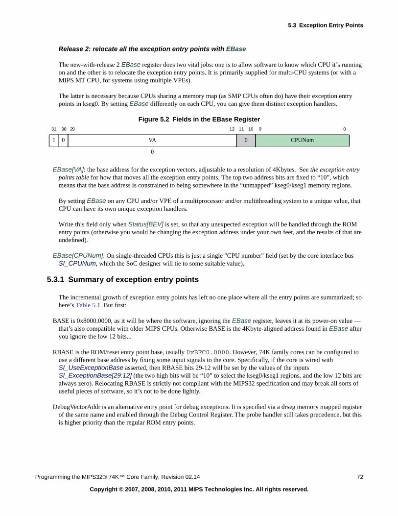
5.3 Exception Entry Points
Programming the MIPS32® 74K™ Core Family, Revision 02.14 72
Copyright © 2007, 2008, 2010, 2011 MIPS Technologies Inc. All rights reserved.
Release 2: relocate all the exception entry points with EBase
The new-with-release 2 EBase register does two vital jobs: one is to allow software to know which CPU it’s runningon and the other is to relocate the exception entry points. It is primarily supplied for multi-CPU systems (or with aMIPS MT CPU, for systems using multiple VPEs).
The latter is necessary because CPUs sharing a memory map (as SMP CPUs often do) have their exception entrypoints in kseg0. By setting EBase differently on each CPU, you can give them distinct exception handlers.
Figure 5.2 Fields in the EBase Register
EBase[VA]: the base address for the exception vectors, adjustable to a resolution of 4Kbytes. See the exception entrypoints table for how that moves all the exception entry points. The top two address bits are fixed to “10”, whichmeans that the base address is constrained to being somewhere in the “unmapped” kseg0/kseg1 memory regions.
By setting EBase on any CPU and/or VPE of a multiprocessor and/or multithreading system to a unique value, thatCPU can have its own unique exception handlers.
Write this field only when Status[BEV] is set, so that any unexpected exception will be handled through the ROMentry points (otherwise you would be changing the exception address under your own feet, and the results of that areundefined).
EBase[CPUNum]: On single-threaded CPUs this is just a single "CPU number" field (set by the core interface busSI_CPUNum, which the SoC designer will tie to some suitable value).
5.3.1 Summary of exception entry points
The incremental growth of exception entry points has left no one place where all the entry points are summarized; sohere’s Table 5.1. But first:
BASE is 0x8000.0000, as it will be where the software, ignoring the EBase register, leaves it at its power-on value —that’s also compatible with older MIPS CPUs. Otherwise BASE is the 4Kbyte-aligned address found in EBase afteryou ignore the low 12 bits...
RBASE is the ROM/reset entry point base, usually 0xBFC0.0000. However, 74K family cores can be configured touse a different base address by fixing some input signals to the core. Specifically, if the core is wired withSI_UseExceptionBase asserted, then RBASE bits 29-12 will be set by the values of the inputsSI_ExceptionBase[29:12] (the two high bits will be “10” to select the kseg0/kseg1 regions, and the low 12 bits arealways zero). Relocating RBASE is strictly not compliant with the MIPS32 specification and may break all sorts ofuseful pieces of software, so it’s not to be done lightly.
DebugVectorAddr is an alternative entry point for debug exceptions. It is specified via a drseg memory mapped registerof the same name and enabled through the Debug Control Register. The probe handler still takes precedence, but thisis higher priority than the regular ROM entry points.
31 30 29 12 11 10 9 0
1 0 VA 0 CPUNum
0
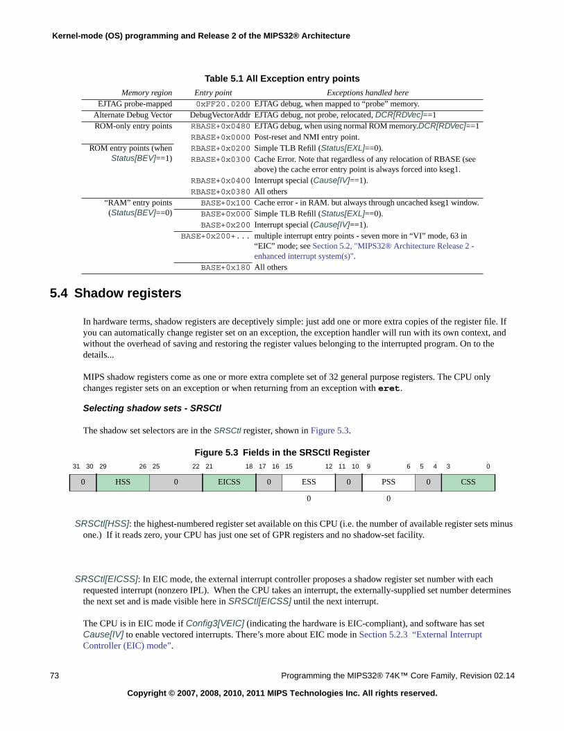
Kernel-mode (OS) programming and Release 2 of the MIPS32® Architecture
73 Programming the MIPS32® 74K™ Core Family, Revision 02.14
Copyright © 2007, 2008, 2010, 2011 MIPS Technologies Inc. All rights reserved.
5.4 Shadow registers
In hardware terms, shadow registers are deceptively simple: just add one or more extra copies of the register file. Ifyou can automatically change register set on an exception, the exception handler will run with its own context, andwithout the overhead of saving and restoring the register values belonging to the interrupted program. On to thedetails...
MIPS shadow registers come as one or more extra complete set of 32 general purpose registers. The CPU onlychanges register sets on an exception or when returning from an exception with eret.
Selecting shadow sets - SRSCtl
The shadow set selectors are in the SRSCtl register, shown in Figure 5.3.
Figure 5.3 Fields in the SRSCtl Register
SRSCtl[HSS]: the highest-numbered register set available on this CPU (i.e. the number of available register sets minusone.) If it reads zero, your CPU has just one set of GPR registers and no shadow-set facility.
SRSCtl[EICSS]: In EIC mode, the external interrupt controller proposes a shadow register set number with eachrequested interrupt (nonzero IPL). When the CPU takes an interrupt, the externally-supplied set number determinesthe next set and is made visible here in SRSCtl[EICSS] until the next interrupt.
The CPU is in EIC mode if Config3[VEIC] (indicating the hardware is EIC-compliant), and software has setCause[IV] to enable vectored interrupts. There’s more about EIC mode in Section 5.2.3 “External InterruptController (EIC) mode”.
Table 5.1 All Exception entry pointsMemory region Entry point Exceptions handled here
EJTAG probe-mapped 0xFF20.0200 EJTAG debug, when mapped to “probe” memory.Alternate Debug Vector DebugVectorAddr EJTAG debug, not probe, relocated, DCR[RDVec]==1ROM-only entry points RBASE+0x0480 EJTAG debug, when using normal ROM memory.DCR[RDVec]==1
RBASE+0x0000 Post-reset and NMI entry point.ROM entry points (when
Status[BEV]==1)RBASE+0x0200 Simple TLB Refill (Status[EXL]==0).RBASE+0x0300 Cache Error. Note that regardless of any relocation of RBASE (see
above) the cache error entry point is always forced into kseg1.RBASE+0x0400 Interrupt special (Cause[IV]==1).RBASE+0x0380 All others
“RAM” entry points(Status[BEV]==0)
BASE+0x100 Cache error - in RAM. but always through uncached kseg1 window.BASE+0x000 Simple TLB Refill (Status[EXL]==0).BASE+0x200 Interrupt special (Cause[IV]==1).
BASE+0x200+... multiple interrupt entry points - seven more in “VI” mode, 63 in“EIC” mode; see Section 5.2, "MIPS32® Architecture Release 2 -enhanced interrupt system(s)".
BASE+0x180 All others
31 30 29 26 25 22 21 18 17 16 15 12 11 10 9 6 5 4 3 0
0 HSS 0 EICSS 0 ESS 0 PSS 0 CSS
0 0
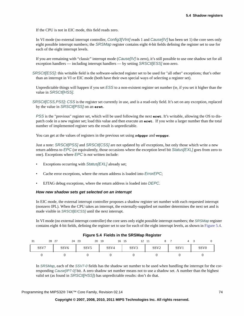
5.4 Shadow registers
Programming the MIPS32® 74K™ Core Family, Revision 02.14 74
Copyright © 2007, 2008, 2010, 2011 MIPS Technologies Inc. All rights reserved.
If the CPU is not in EIC mode, this field reads zero.
In VI mode (no external interrupt controller, Config3[VInt] reads 1 and Cause[IV] has been set 1) the core sees onlyeight possible interrupt numbers; the SRSMap register contains eight 4-bit fields defining the register set to use foreach of the eight interrupt levels.
If you are remaining with “classic” interrupt mode (Cause[IV] is zero), it’s still possible to use one shadow set for allexception handlers — including interrupt handlers — by setting SRSCtl[ESS] non-zero.
SRSCtl[ESS]: this writable field is the software-selected register set to be used for "all other" exceptions; that’s otherthan an interrupt in VI or EIC mode (both have their own special ways of selecting a register set).
Unpredictable things will happen if you set ESS to a non-existent register set number (ie, if you set it higher than thevalue in SRSCtl[HSS].
SRSCtl[CSS,PSS]: CSS is the register set currently in use, and is a read-only field. It’s set on any exception, replacedby the value in SRSCtl[PSS] on an eret.
PSS is the "previous" register set, which will be used following the next eret. It’s writable, allowing the OS to dis-patch code in a new register set; load this value and then execute an eret. If you write a larger number than the totalnumber of implemented register sets the result is unpredictable.
You can get at the values of registers in the previous set using rdpgpr and wrpgpr.
Just a note: SRSCtl[PSS] and SRSCtl[CSS] are not updated by all exceptions, but only those which write a newreturn address to EPC (or equivalently, those occasions where the exception level bit Status[EXL] goes from zero toone). Exceptions where EPC is not written include:
• Exceptions occurring with Status[EXL] already set;
• Cache error exceptions, where the return address is loaded into ErrorEPC;
• EJTAG debug exceptions, where the return address is loaded into DEPC.
How new shadow sets get selected on an interrupt
In EIC mode, the external interrupt controller proposes a shadow register set number with each requested interrupt(nonzero IPL). When the CPU takes an interrupt, the externally-supplied set number determines the next set and ismade visible in SRSCtl[EICSS] until the next interrupt.
In VI mode (no external interrupt controller) the core sees only eight possible interrupt numbers; the SRSMap registercontains eight 4-bit fields, defining the register set to use for each of the eight interrupt levels, as shown in Figure 5.4.
Figure 5.4 Fields in the SRSMap Register
In SRSMap, each of the SSV7-0 fields has the shadow set number to be used when handling the interrupt for the cor-responding Cause[IP7-0] bit. A zero shadow set number means not to use a shadow set. A number than the highestvalid set (as found in SRSCtl[HSS]) has unpredictable results: don’t do that.
31 28 27 24 23 20 19 16 15 12 11 8 7 4 3 0
SSV7 SSV6 SSV5 SSV4 SSV3 SSV2 SSV1 SSV0
0 0 0 0 0 0 0 0
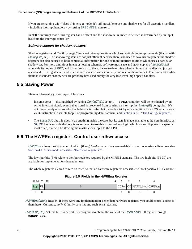
Kernel-mode (OS) programming and Release 2 of the MIPS32® Architecture
75 Programming the MIPS32® 74K™ Core Family, Revision 02.14
Copyright © 2007, 2008, 2010, 2011 MIPS Technologies Inc. All rights reserved.
If you are remaining with “classic” interrupt mode, it’s still possible to use one shadow set for all exception handlers- including interrupt handlers - by setting SRSCtl[ESS] non-zero.
In “EIC” interrupt mode, this register has no effect and the shadow set number to be used is determined by an inputbus from the interrupt controller.
Software support for shadow registers
Shadow registers work “as if by magic” for short interrupt routines which run entirely in exception mode (that is, withStatus[EXL] set). The shadow registers are not just efficient because there’s no need to save user registers; the shadowregisters can also be used to hold contextual information for one or more interrupt routines which uses a particularshadow set. For more ambitious interrupt nesting schemes, software must save and stack copies of SRSCtl[PSS]alongside its copies of EPC; and it’s entirely up to the software to determine when an interrupt handler can just goahead and use a register set, and when it needs to save values on entry and restore them on exit. That’s at least as dif-ficult as it sounds: shadow sets are probably best used purely for very low-level, high-speed handlers.
5.5 Saving Power
There are basically just a couple of facilities:
In some cores — distinguished by having Config7[WII] set to 1 — a wait condition will be terminated by anactive interrupt signal, even if that signal is prevented from causing an interrupt by Status[IE] being clear. It’snot immediately obvious why that behavior is useful, but it avoids a tricky race condition for an OS which uses await instruction in its idle loop. For programming details consult and Section B.2.1 “The Config7 register”.
• The Status[RP] bit: this doesn’t do anything inside the core, but its state is made available at the core interface asSI_RP. Logic outside the core is encouraged to use this to control any logic which trades off power for speed -most often, that will be slowing the master clock input to the CPU.
5.6 The HWREna register - Control user rdhwr access
HWREna allows the OS to control which (if any) hardware registers are readable in user mode using rdhwr: see alsoSection 4.1 “User-mode accessible “Hardware registers””.
The low four bits (3-0) relate to the four registers required by the MIPS32 standard. The two high bits (31-30) areavailable for implementation-dependent use.
The whole register is cleared to zero on reset, so that no hardware register is accessible without positive OS clearance.
Figure 5.5 Fields in the HWREna Register
HWREna[Impl]: Read 0. If there were any implementation-dependent hardware registers, you could control access tothem here. Currently, no 74K family core has any such extra registers.
HWREna[UL]: Set this bit 1 to permit user programs to obtain the value of the UserLocal CP0 register throughrdhwr $29.
31 30 29 28 4 3 2 1 0
Impl UL 0 CCRes CC SYNCI_Step CPUNum
0 0 0 0 0 0
5.6 The HWREna register - Control user rdhwr access
Programming the MIPS32® 74K™ Core Family, Revision 02.14 76
Copyright © 2007, 2008, 2010, 2011 MIPS Technologies Inc. All rights reserved.
HWREna[CCRes]: Set this bit 1 so a user-mode rdhwr 3 can determine whether Count runs at the full clock rate orsome divisor.
HWREna[CC]: Set this bit 1 so a user-mode rdhwr 2 can read out the value of the Count register.
HWREna[SYNCI_Step]: Set this bit 1 so a user-mode rdhwr 1 can read out the cache line size (actually, the smallerof the L1 I-cache line size and D-cache line size). That line size determines the step between successive uses of thesynci instruction, which does the cache manipulation necessary to ensure that the CPU can correctly executeinstructions which you just wrote.
HWREna[CPUNum]: Set this bit 1 so a user-mode rdhwr 0 reads out the CPU ID number, as found inEBase[CPUNum].
Chapter 6
Programming the MIPS32® 74K™ Core Family, Revision 02.14 77
Copyright © 2007, 2008, 2010, 2011 MIPS Technologies Inc. All rights reserved.
Floating point unit
The 74Kf™ member of the 74K family has a hardware floating point unit (FPU). This:
• Is a 64-bit FPU: with instructions working on both 64-bit and 32-bit floating point numbers, whose formats arecompatible with the “double precision” and “single precision” recommendations of [IEEE754].
• Is compatible with the MIPS64 Architecture: implements the floating point instruction set defined in[MIPS64V2]; because the 74K family integer core is a 32-bit processor, a couple of additional instructionsmfhc1 and mthc1 are available to help pack and unpack 64-bit values when copying data between integer andFP registers - see Section C.3 “FPU changes in Release 2 of the MIPS32® Architecture” or for full details[MIPS32].
• Usually runs at half or two-thirds of the integer core’s clock rate: the design is tested to work with the FPU run-ning at the core speed, but in likely processes the FPU will then limit the achievable frequency of the whole core.You can query the Config7[FPR,FPR1] fields in Section B.2.1 “The Config7 register” to check which option isused on your CPU.
• Can run without an exception handler: the FPU offers a range of options to handle very large and very smallnumbers in hardware. With the 74K core full IEEE754 compliance does require that some operand/operationcombinations be trapped and emulated, but high performance and good accuracy are available with settingswhich get the hardware to do everything - see Section 6.4.2, "FPU “unimplemented” exceptions (and how toavoid them)".
• Omits “paired single” and MIPS-3D extensions: those are primarily aimed at 3D graphics, and are described asoptional in [MIPS64V2].
• Uses an autonomous 7-stage pipeline: all data transfers are interlocked, so the programmer is never aware of thepipeline. Compiler writers and daemon subroutine tuners do need to know: there’s timing information in Section6.5, "FPU pipeline and instruction timing".
• Has limited dual issue: the FPU has two parallel pipelines, and under optimum conditions can issue two instruc-tions simultaneously. One handles all arithmetic operations, the other deals with loads, stores and data transfersto/from integer registers.
6.1 Data representation
If you’d like to read up on floating point in general you might like to read [SEEMIPSRUN]:. But it’s probably usefulto remind you (in Figure 6.1) what 32-bit and 64-bit floating point numbers on MIPS architecture CPUs look like.
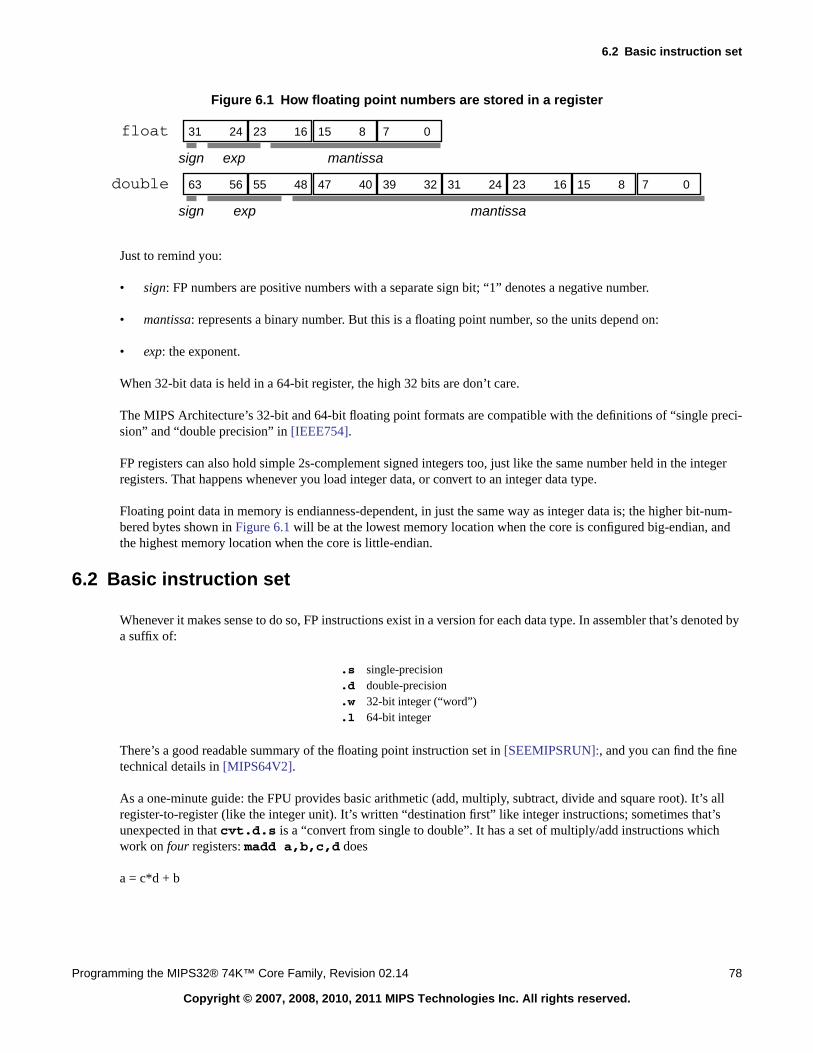
6.2 Basic instruction set
Programming the MIPS32® 74K™ Core Family, Revision 02.14 78
Copyright © 2007, 2008, 2010, 2011 MIPS Technologies Inc. All rights reserved.
Figure 6.1 How floating point numbers are stored in a register
Just to remind you:
• sign: FP numbers are positive numbers with a separate sign bit; “1” denotes a negative number.
• mantissa: represents a binary number. But this is a floating point number, so the units depend on:
• exp: the exponent.
When 32-bit data is held in a 64-bit register, the high 32 bits are don’t care.
The MIPS Architecture’s 32-bit and 64-bit floating point formats are compatible with the definitions of “single preci-sion” and “double precision” in [IEEE754].
FP registers can also hold simple 2s-complement signed integers too, just like the same number held in the integerregisters. That happens whenever you load integer data, or convert to an integer data type.
Floating point data in memory is endianness-dependent, in just the same way as integer data is; the higher bit-num-bered bytes shown in Figure 6.1 will be at the lowest memory location when the core is configured big-endian, andthe highest memory location when the core is little-endian.
6.2 Basic instruction set
Whenever it makes sense to do so, FP instructions exist in a version for each data type. In assembler that’s denoted bya suffix of:
There’s a good readable summary of the floating point instruction set in [SEEMIPSRUN]:, and you can find the finetechnical details in [MIPS64V2].
As a one-minute guide: the FPU provides basic arithmetic (add, multiply, subtract, divide and square root). It’s allregister-to-register (like the integer unit). It’s written “destination first” like integer instructions; sometimes that’sunexpected in that cvt.d.s is a “convert from single to double”. It has a set of multiply/add instructions whichwork on four registers: madd a,b,c,d does
a = c*d + b
.s single-precision
.d double-precision
.w 32-bit integer (“word”)
.l 64-bit integer
float
double
1623 815 07
mantissasign exp
2431
5663 323940474855 16232431 815 07
mantissasign exp
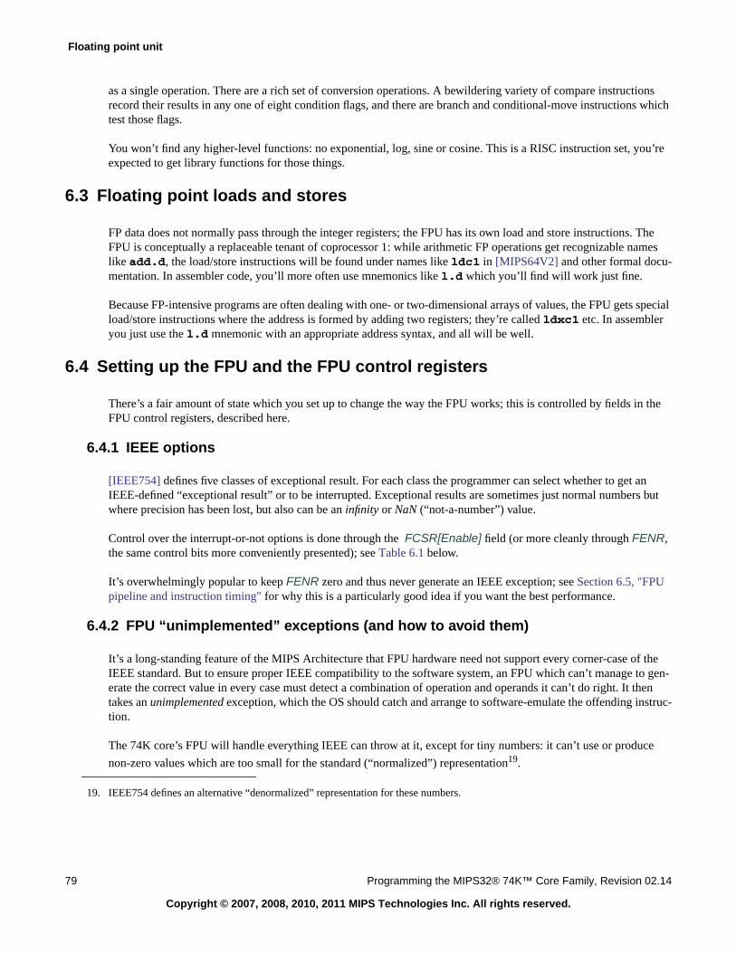
Floating point unit
79 Programming the MIPS32® 74K™ Core Family, Revision 02.14
Copyright © 2007, 2008, 2010, 2011 MIPS Technologies Inc. All rights reserved.
as a single operation. There are a rich set of conversion operations. A bewildering variety of compare instructionsrecord their results in any one of eight condition flags, and there are branch and conditional-move instructions whichtest those flags.
You won’t find any higher-level functions: no exponential, log, sine or cosine. This is a RISC instruction set, you’reexpected to get library functions for those things.
6.3 Floating point loads and stores
FP data does not normally pass through the integer registers; the FPU has its own load and store instructions. TheFPU is conceptually a replaceable tenant of coprocessor 1: while arithmetic FP operations get recognizable nameslike add.d, the load/store instructions will be found under names like ldc1 in [MIPS64V2] and other formal docu-mentation. In assembler code, you’ll more often use mnemonics like l.d which you’ll find will work just fine.
Because FP-intensive programs are often dealing with one- or two-dimensional arrays of values, the FPU gets specialload/store instructions where the address is formed by adding two registers; they’re called ldxc1 etc. In assembleryou just use the l.d mnemonic with an appropriate address syntax, and all will be well.
6.4 Setting up the FPU and the FPU control registers
There’s a fair amount of state which you set up to change the way the FPU works; this is controlled by fields in theFPU control registers, described here.
6.4.1 IEEE options
[IEEE754] defines five classes of exceptional result. For each class the programmer can select whether to get anIEEE-defined “exceptional result” or to be interrupted. Exceptional results are sometimes just normal numbers butwhere precision has been lost, but also can be an infinity or NaN (“not-a-number”) value.
Control over the interrupt-or-not options is done through the FCSR[Enable] field (or more cleanly through FENR,the same control bits more conveniently presented); see Table 6.1 below.
It’s overwhelmingly popular to keep FENR zero and thus never generate an IEEE exception; see Section 6.5, "FPUpipeline and instruction timing" for why this is a particularly good idea if you want the best performance.
6.4.2 FPU “unimplemented” exceptions (and how to avoid them)
It’s a long-standing feature of the MIPS Architecture that FPU hardware need not support every corner-case of theIEEE standard. But to ensure proper IEEE compatibility to the software system, an FPU which can’t manage to gen-erate the correct value in every case must detect a combination of operation and operands it can’t do right. It thentakes an unimplemented exception, which the OS should catch and arrange to software-emulate the offending instruc-tion.
The 74K core’s FPU will handle everything IEEE can throw at it, except for tiny numbers: it can’t use or produce
non-zero values which are too small for the standard (“normalized”) representation19.
19. IEEE754 defines an alternative “denormalized” representation for these numbers.
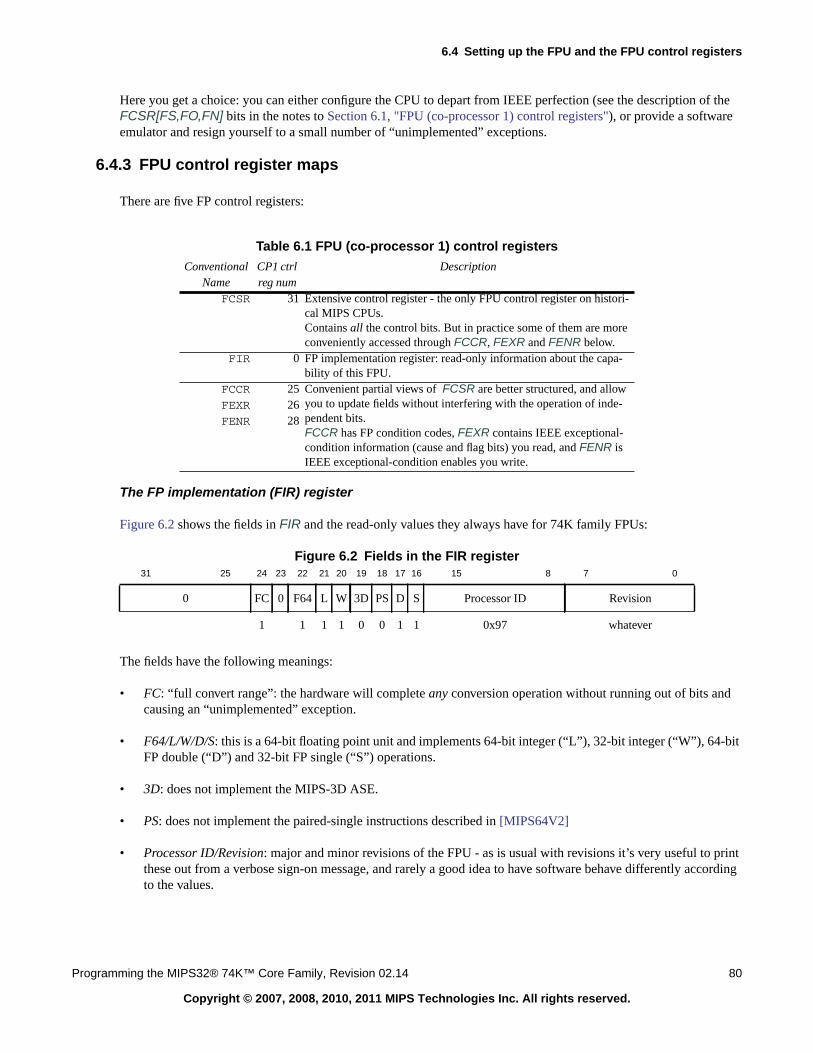
6.4 Setting up the FPU and the FPU control registers
Programming the MIPS32® 74K™ Core Family, Revision 02.14 80
Copyright © 2007, 2008, 2010, 2011 MIPS Technologies Inc. All rights reserved.
Here you get a choice: you can either configure the CPU to depart from IEEE perfection (see the description of theFCSR[FS,FO,FN] bits in the notes to Section 6.1, "FPU (co-processor 1) control registers"), or provide a softwareemulator and resign yourself to a small number of “unimplemented” exceptions.
6.4.3 FPU control register maps
There are five FP control registers:
The FP implementation (FIR) register
Figure 6.2 shows the fields in FIR and the read-only values they always have for 74K family FPUs:
Figure 6.2 Fields in the FIR register
The fields have the following meanings:
• FC: “full convert range”: the hardware will complete any conversion operation without running out of bits andcausing an “unimplemented” exception.
• F64/L/W/D/S: this is a 64-bit floating point unit and implements 64-bit integer (“L”), 32-bit integer (“W”), 64-bitFP double (“D”) and 32-bit FP single (“S”) operations.
• 3D: does not implement the MIPS-3D ASE.
• PS: does not implement the paired-single instructions described in [MIPS64V2]
• Processor ID/Revision: major and minor revisions of the FPU - as is usual with revisions it’s very useful to printthese out from a verbose sign-on message, and rarely a good idea to have software behave differently accordingto the values.
Table 6.1 FPU (co-processor 1) control registersConventional CP1 ctrl Description
Name reg numFCSR 31 Extensive control register - the only FPU control register on histori-
cal MIPS CPUs.Contains all the control bits. But in practice some of them are moreconveniently accessed through FCCR, FEXR and FENR below.
FIR 0 FP implementation register: read-only information about the capa-bility of this FPU.
FCCR 25 Convenient partial views of FCSR are better structured, and allowyou to update fields without interfering with the operation of inde-pendent bits.FCCR has FP condition codes, FEXR contains IEEE exceptional-condition information (cause and flag bits) you read, and FENR isIEEE exceptional-condition enables you write.
FEXR 26FENR 28
31 25 24 23 22 21 20 19 18 17 16 15 8 7 0
0 FC 0 F64 L W 3D PS D S Processor ID Revision
1 1 1 1 0 0 1 1 0x97 whatever
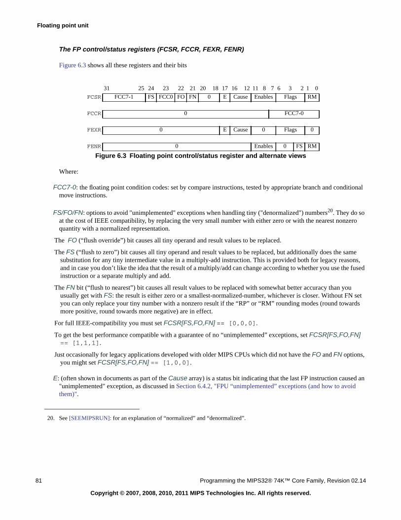
Floating point unit
81 Programming the MIPS32® 74K™ Core Family, Revision 02.14
Copyright © 2007, 2008, 2010, 2011 MIPS Technologies Inc. All rights reserved.
The FP control/status registers (FCSR, FCCR, FEXR, FENR)
Figure 6.3 shows all these registers and their bits
Where:
FCC7-0: the floating point condition codes: set by compare instructions, tested by appropriate branch and conditionalmove instructions.
FS/FO/FN: options to avoid "unimplemented" exceptions when handling tiny ("denormalized") numbers20. They do soat the cost of IEEE compatibility, by replacing the very small number with either zero or with the nearest nonzeroquantity with a normalized representation.
The FO (“flush override”) bit causes all tiny operand and result values to be replaced.
The FS (“flush to zero”) bit causes all tiny operand and result values to be replaced, but additionally does the samesubstitution for any tiny intermediate value in a multiply-add instruction. This is provided both for legacy reasons,and in case you don’t like the idea that the result of a multiply/add can change according to whether you use the fusedinstruction or a separate multiply and add.
The FN bit (“flush to nearest”) bit causes all result values to be replaced with somewhat better accuracy than youusually get with FS: the result is either zero or a smallest-normalized-number, whichever is closer. Without FN setyou can only replace your tiny number with a nonzero result if the “RP” or “RM” rounding modes (round towardsmore positive, round towards more negative) are in effect.
For full IEEE-compatibility you must set FCSR[FS,FO,FN] == [0,0,0].
To get the best performance compatible with a guarantee of no “unimplemented” exceptions, set FCSR[FS,FO,FN]== [1,1,1].
Just occasionally for legacy applications developed with older MIPS CPUs which did not have the FO and FN options,you might set FCSR[FS,FO,FN] == [1,0,0].
E: (often shown in documents as part of the Cause array) is a status bit indicating that the last FP instruction caused an"unimplemented" exception, as discussed in Section 6.4.2, "FPU “unimplemented” exceptions (and how to avoidthem)".
31 25 24 23 22 21 20 18 17 16 12 11 8 7 6 3 2 1 0
FCSR FCC7-1 FS FCC0 FO FN 0 E Cause Enables Flags RM
FCCR 0 FCC7-0
FEXR 0 E Cause 0 Flags 0
FENR 0 Enables 0 FS RM
Figure 6.3 Floating point control/status register and alternate views
20. See [SEEMIPSRUN]: for an explanation of “normalized” and “denormalized”.
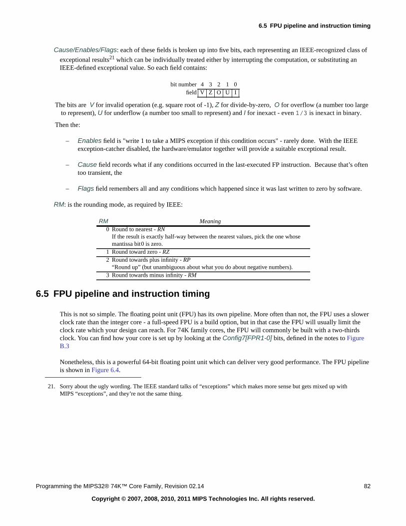
6.5 FPU pipeline and instruction timing
Programming the MIPS32® 74K™ Core Family, Revision 02.14 82
Copyright © 2007, 2008, 2010, 2011 MIPS Technologies Inc. All rights reserved.
Cause/Enables/Flags: each of these fields is broken up into five bits, each representing an IEEE-recognized class of
exceptional results21 which can be individually treated either by interrupting the computation, or substituting anIEEE-defined exceptional value. So each field contains:
The bits are V for invalid operation (e.g. square root of -1), Z for divide-by-zero, O for overflow (a number too largeto represent), U for underflow (a number too small to represent) and I for inexact - even 1/3 is inexact in binary.
Then the:
– Enables field is "write 1 to take a MIPS exception if this condition occurs" - rarely done. With the IEEEexception-catcher disabled, the hardware/emulator together will provide a suitable exceptional result.
– Cause field records what if any conditions occurred in the last-executed FP instruction. Because that’s oftentoo transient, the
– Flags field remembers all and any conditions which happened since it was last written to zero by software.
RM: is the rounding mode, as required by IEEE:
6.5 FPU pipeline and instruction timing
This is not so simple. The floating point unit (FPU) has its own pipeline. More often than not, the FPU uses a slowerclock rate than the integer core - a full-speed FPU is a build option, but in that case the FPU will usually limit theclock rate which your design can reach. For 74K family cores, the FPU will commonly be built with a two-thirdsclock. You can find how your core is set up by looking at the Config7[FPR1-0] bits, defined in the notes to FigureB.3
Nonetheless, this is a powerful 64-bit floating point unit which can deliver very good performance. The FPU pipelineis shown in Figure 6.4.
21. Sorry about the ugly wording. The IEEE standard talks of “exceptions” which makes more sense but gets mixed up withMIPS “exceptions”, and they’re not the same thing.
bit number 4 3 2 1 0field V Z O U I
RM Meaning0 Round to nearest - RN
If the result is exactly half-way between the nearest values, pick the one whosemantissa bit0 is zero.
1 Round toward zero - RZ2 Round towards plus infinity - RP
“Round up” (but unambiguous about what you do about negative numbers).3 Round towards minus infinity - RM
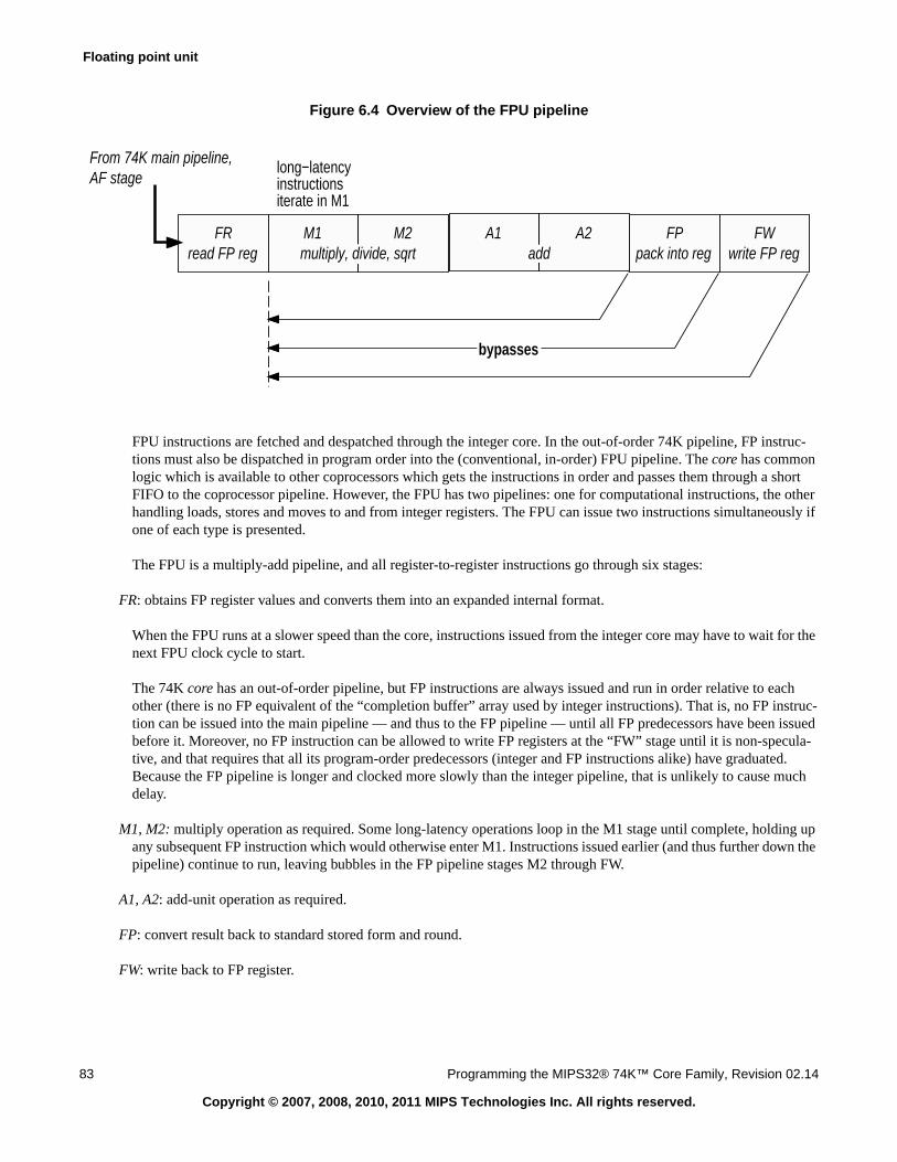
Floating point unit
83 Programming the MIPS32® 74K™ Core Family, Revision 02.14
Copyright © 2007, 2008, 2010, 2011 MIPS Technologies Inc. All rights reserved.
Figure 6.4 Overview of the FPU pipeline
FPU instructions are fetched and despatched through the integer core. In the out-of-order 74K pipeline, FP instruc-tions must also be dispatched in program order into the (conventional, in-order) FPU pipeline. The core has commonlogic which is available to other coprocessors which gets the instructions in order and passes them through a shortFIFO to the coprocessor pipeline. However, the FPU has two pipelines: one for computational instructions, the otherhandling loads, stores and moves to and from integer registers. The FPU can issue two instructions simultaneously ifone of each type is presented.
The FPU is a multiply-add pipeline, and all register-to-register instructions go through six stages:
FR: obtains FP register values and converts them into an expanded internal format.
When the FPU runs at a slower speed than the core, instructions issued from the integer core may have to wait for thenext FPU clock cycle to start.
The 74K core has an out-of-order pipeline, but FP instructions are always issued and run in order relative to eachother (there is no FP equivalent of the “completion buffer” array used by integer instructions). That is, no FP instruc-tion can be issued into the main pipeline — and thus to the FP pipeline — until all FP predecessors have been issuedbefore it. Moreover, no FP instruction can be allowed to write FP registers at the “FW” stage until it is non-specula-tive, and that requires that all its program-order predecessors (integer and FP instructions alike) have graduated.Because the FP pipeline is longer and clocked more slowly than the integer pipeline, that is unlikely to cause muchdelay.
M1, M2: multiply operation as required. Some long-latency operations loop in the M1 stage until complete, holding upany subsequent FP instruction which would otherwise enter M1. Instructions issued earlier (and thus further down thepipeline) continue to run, leaving bubbles in the FP pipeline stages M2 through FW.
A1, A2: add-unit operation as required.
FP: convert result back to standard stored form and round.
FW: write back to FP register.
bypasses
FRread FP reg
FPpack into reg
FWwrite FP reg
M1 M2 A1 A2addmultiply, divide, sqrt
long−latencyinstructions iterate in M1
From 74K main pipeline,AF stage
6.5 FPU pipeline and instruction timing
Programming the MIPS32® 74K™ Core Family, Revision 02.14 84
Copyright © 2007, 2008, 2010, 2011 MIPS Technologies Inc. All rights reserved.
6.5.1 FPU register dependency delays
Any FPU instruction must go through pipeline stages from M1 through A2 before it produces a result, which can then(as shown by the “bypass” lines in the pipeline diagram) be used by a dependent instruction reaching the M1 stage. Ifyou want to keep the FPU pipeline full, that means it’s enough to have three non-dependent instructions between theconsumer and producer of an FP value. However, there’s no guarantee that all the FP pipeline slots will be filled, andthen three intervening instructions will be excessive. Good compilers should try to schedule FP instructions, but not atunreasonable cost.
6.5.2 Delays caused by long-latency instructions looping in the M1 stage
Instructions which take only one clock in M1 go through the pipeline smoothly and can be completed one per FPUclock period. Instructions which take longer in M1 always prevent the next instruction from starting in the next clock,regardless of any data dependency. Those long-latency instructions - double-precision multiplies and all division andsquare root operations - are listed in Table 6.2. An instruction which runs for 2 cycles in M1 holds up the FPU pipe-line for one clock and so on - and of course the cycle counts are for FPU cycles.
6.5.3 Delays on FP load and store instructions
FP store instructions graduate from the main pipeline (subject to dependencies and freedom from address excep-tions), and then wait in a special queue until FP data is delivered. The store data will be significantly delayed com-pared to an integer store instruction: but unless some other instruction reads the target cache line, the program willprobably not see much delay.
FP load instructions in the main pipeline are treated like integer loads; an FP load which hits in the cache can be com-pleted in the main pipeline. The load data is passed from D-cache into the FPU pipeline, and you should see no morethan the usual FP producer-consumer delay from load to use. FPU load instructions which miss are processed in thememory pipeline. FP loads are non-blocking too, so it will be the consuming instruction (if any) which is delayed.
6.5.4 Delays when main pipeline waits for FPU to decide not to take an exception
The MIPS architecture requires FP exceptions to be “precise”, which (in particular) means that no instruction afterthe FP instruction causing the exception may do anything software-visible. That means that an FP instruction in themain pipeline may not be committed, nor leave the main pipeline, until the FPU can either report the exception, orconfirm that the instruction will not cause an exception.
Floating point instructions cause exceptions not only because a user program has requested the system to trap IEEEexceptional conditions (which is unusual) but also because the hardware is not capable of generating or acceptingvery small (“denormalized”) numbers in accordance with the IEEE standards. The latter (“unimplemented”) excep-tion is used to call up a software emulator to patch up some rare cases. But the main pipeline must be stalled until the
Table 6.2 Long-latency FP instructionsOperand Instruction type Instructions Cycles in M1
Double-precision (64-bit) Any multiplication mul.d,madd.d, msub.d,nmadd.d, nmsub.d 2
Single-precision (32-bit) Reciprocal recip.s 10
divide, square-root div.s,sqrt.s 14
reciprocal square root rsqrt.s 14
Double-precision (64-bit) Reciprocal recip.d 21
divide, square-root div.d,sqrt.d 29
reciprocal square root rsqrt.d 31
Floating point unit
85 Programming the MIPS32® 74K™ Core Family, Revision 02.14
Copyright © 2007, 2008, 2010, 2011 MIPS Technologies Inc. All rights reserved.
FP hardware can rule out an exception, and that leads to a delay on every non-trivial FP operation. With a half-rateFPU, this stall will most likely be 6-7 clocks.
Software which can tolerate some deviation from IEEE precision can avoid these delays by opting to replace alldenormalized inputs and results by zero - controlled by the FCSR[FS,FO,FN] register bits described in Section 6.1,"FPU (co-processor 1) control registers" and its notes. If you have also disabled all IEEE traps, you get no possibilityof FP exceptions and no extra main pipeline delay.
6.5.5 Delays when main pipeline waits for FPU to accept an instruction
FP instructions are queued (some queues are shared with other co-processors, if fitted) for transmission to the FPUhardware. If that queue (which has 8 entries) fills up, the CPU will be unable to issue more FP instructions — andsince FP instructions are issued in-order, that will quickly clog up the CPU
6.5.6 Delays on mfc1/mtc1 instructions
mtc1 goes down the main pipe and gets its GP register data just like any other instruction (from the register file, acompletion buffer or a by-pass): then it passes it across to the FPU. In the FPU pipeline, the mtc1 looks like an FPload which hits: the data is sent to the FP unit a predictable number of cycles after it is issued
mfc1 (in the FPU pipeline) resembles a FP store. The FP data is sent back the same FPU-to-EU data path as is usedin a store, but then written into the CB which belongs to the integer AGEN pipeline’s version of the same mfc1instruction. The timing is awkward because you have to find a free completion buffer write port. Once the data is inthe CB, the mfc1 is a candidate for graduation. Since the FPU pipeline is long and it usually runs slower than theinteger pipeline, the effective latency of mfc1 can be high. A program will run faster if the mfc1 can be placed 10-15instruction positions ahead of its consumer.
6.5.7 Delays caused by dependency on FPU status register fields
The conditional branch instructions bc1f/bc1t and the conditional moves movf/movt execute in the main pipe-line, but test a FP condition bit generated by the various FPU compare instructions.
bc1f/bc1t (like other conditional branches) are executed speculatively in the execution unit. FP condition valuesare not passed through CBs, so the check for a mispredict is not made until the branch instruction tries to graduate.That means that mispredicted FP branches are a couple of cycles more expensive than regular mispredictions.
MIPS recommends that you don’t use the “branch likely” (bc1fl/bc1tl) versions of these instructions in new code.
6.5.8 Slower operation in MIPS I™ compatibility mode
Historic 32-bit MIPS CPUs had only 16 “even-numbered” floating point registers usable for arithmetic, with odd-numbered registers working together with them to let you load, store and transfer double-precision (64-bit) values.Software written for those old CPUs is incompatible with the full modern FPU, so there’s a compatibility bit providedin Status[FR] - set zero to use MIPS I compatible code. This comes at the cost of slower repeat rates for FP instruc-tions, because in compatibility mode not all the bypasses shown in the pipeline diagram above are active.
6.5 FPU pipeline and instruction timing
Programming the MIPS32® 74K™ Core Family, Revision 02.14 86
Copyright © 2007, 2008, 2010, 2011 MIPS Technologies Inc. All rights reserved.
Chapter 7
Programming the MIPS32® 74K™ Core Family, Revision 02.14 87
Copyright © 2007, 2008, 2010, 2011 MIPS Technologies Inc. All rights reserved.
The MIPS32® DSP ASE
The MIPS DSP ASE is provided to accelerate a large range of DSP algorithms. You can get most programming infor-mation from this chapter. There’s more detail in the formal DSP ASE specification [MIPSDSP], but expect to readthrough lots of material aimed at hardware implementors. You may also find [DSPWP] useful for tips and examplesof converting DSP algorithms for the DSP ASE.
Different target applications generally need different data size and precision:
• 32-bit data: audio (non-hand-held) decoding/encoding - a wide range of “hi-fi” standards for consumer audio ortelevision sound.
Raw audio data (as found on CD) is 16-bit; but if you do your processing in 16 bits you lose precision beyondwhat is acceptable for hi-fi.
• 16-bit data: digital voice for telephony. International telephony code/decode standards include G.723.1(8Ksample/s, 5-6Kbit/s data rate, 37ms delay), G.729 (8Kbit/s, 15ms delay) and G.726 (16-40Kbit/s, computa-tionally simpler and higher quality, good for carrying analogue modem tones). Application-specific filters areused for echo cancellation, noise cancellation, and channel equalization.
Also used for soft modems and much general “DSP” work (filters, correlation, convolution); lo-fi devices use 16bits for audio.
• 8-bit data: processing of printer images, JPEG (still) images and video data.
7.1 Features provided by the MIPS® DSP ASE
Those target applications can benefit from unconventional architecture features because they rely on:
• Fixed-point fractional data types: It is not yet economical (in terms of either chip size or power budget) to usefloating point calculations in these contexts. DSP applications use fixed-point fractions. Such a fraction is just asigned integer, but understood to represent that integer divided by some power of two. A 32-bit fractional format
where the implicit divisor is 216 (65536) would be referred to as a Q15.16 format; that’s because there are 16 bitsdevoted to fractional precision and 15 bits to the whole number range (the highest bit does duty as a sign bit andisn’t counted).
With this notation Q31.0 is a conventional signed integer, and Q0.31 is a fraction representing numbers between-1 and 1 (well, nearly 1). It turns out that Q0.31 is the most popular 32-bit format for DSP applications, since itwon’t overflow when multiplied (except in the corner case where -1×-1 leads to the just-too-large value 1).Q0.31 is often abbreviated to Q31.
The DSP ASE provides support for Q31 and Q15 (signed 16-bit) fractions.
• Saturating arithmetic: It’s not practicable to build in overflow checks to DSP algorithms - they need to be toofast. Clever algorithms may be built to be overflow-proof; but not all can be. Often the least worst thing to do
7.2 The DSP ASE control register
Programming the MIPS32® 74K™ Core Family, Revision 02.14 88
Copyright © 2007, 2008, 2010, 2011 MIPS Technologies Inc. All rights reserved.
when a calculation overflows is to make the result the most positive or most negative representable value. Arith-metic which does that is called saturating - and quite a lot of operations in the DSP ASE saturate (in many casesthere are saturating and non-saturating versions of what is otherwise the same instruction).
• Multiplying fractions: if you multiply two Q31 fractions by re-using a full-precision integer multiplier, thenyou’ll get a 64-bit result which consists of a Q62 result with (in the very highest bit) a second copy of the sign bit.This is a bit peculiar, so it’s more useful if you always do a left-shift-by-1 on this value, producing a Q63 format(a more natural way to use 64 bits). Q15 multiplies which generate a Q31 value have to do the shift-left too.That’s what all the mulq... instructions do.
• Rounding: some fractional operations implicitly discard less significant bits. But you get a better approximationif you bump the truncated result by one when the discarded bits represent more than a half of the value of a 1 inthe new LS position. That’s what we mean by rounding in this chapter.
• Multiply-accumulate sequences with choice of four accumulators: (with fixed-point types, sometimes saturating).
The 74K already has quite a slick integer multiply-accumulate operation, but it’s not so efficient when used forfractional and saturating operations.
The sequences are made more usable by having four 64-bit result/accumulator registers - (the old MIPS multiplydivide unit has just one, accessible as the hi/lo registers). The new ac0 is the old hi/lo, for backward compatibility.
• Benefit from “SIMD” operations.: Many DSP calculations are a good match for “Single Instruction MultipleData” or vector operations, where the same arithmetic operation is applied in parallel to several sets of operands.
In the MIPS DSP ASE, some operations are SIMD type - two 16-bit operations or four 8-bit operations are car-ried out in parallel on operands packed into a single 32-bit general-purpose register. Instructions operating onvectors can be recognized because the name includes.ph (paired-half, usually signed, often fractional) or.qb(quad-byte, always unsigned, only occasionally fractional).
The DSP ASE hardware involves an extensive re-work of the normal integer multiply/divide unit. As mentionedabove it has four 64-bit accumulators (not just one) and a new control register, described immediately below.
7.2 The DSP ASE control register
This is a part of the user-mode programming model for the DSP ASE, and is a 32-bit value read and written with therddsp/wrdsp instructions. It holds state information for some DSP sequences.
In Figure 7.1:
ccond: condition bits set by compare instructions (there have to be four to report on compares between vector types)."Compare" operations on scalars or vectors of length two only touch the lower-numbered bits. DSPControl bits 31:28are used for more ccond bits in 64-bit machines.
Figure 7.1 Fields in the DSPControl Register31 28 27 24 23 16 15 14 13 12 7 6 5 0
0 ccond ouflag 0 EFI c scount 0 pos
The MIPS32® DSP ASE
89 Programming the MIPS32® 74K™ Core Family, Revision 02.14
Copyright © 2007, 2008, 2010, 2011 MIPS Technologies Inc. All rights reserved.
ouflag: one of these bits may be set when a result overflows (whether or not the result is saturated depends on theinstruction - the flag is set in either case). The "ou" stands for "overflow/underflow" - "underflow" is used here for avalue which is negative but with excessive absolute value.
Any overflowed/underflowed result produced by any DSP ASE instruction sets a ouflag bit, except for addsc/addwc and shilo/shilov.
The 6 bits are set according to the destination of the operation which overflowed, and the kind of operation itwas:
EFI: set by any of the accumulator-to-register bitfield extract instructions extp, extpv, extpdp, or extpdp. It’s setto 1 if and only if the instruction finds there are insufficient bits to extract. That is, if DSPControl[pos] - which issupposed to mark the highest-numbered bit of the field we’re extracting - is less than the size value specified by theinstruction.
c: Carry bit for 32-bit add/carry instructions addsc and addwc.
scount, pos: Fields for use by "variable" bitfield insert and extract instructions, such as insv (the normal MIPS32ins/ext instructions have the field size and position hard-coded in the instruction).
scount specifies the size of the bit field to be inserted, while pos specifies the insert position.
Caution: in all inserts (following the lead of the standard MIPS32 insert/extract instructions) pos is set to thelowest bit number in the field. But in the DSP ASE extract-from-accumulator instructions (extp, extpv, ext-pdp and extpdpv), pos identifies the highest-numbered bit in the field.
The latter two (“dp”) instructions post-decrement pos (by the bitfield length size), to help software which isunpacking a series of bitfields from a dense data structure.
The mthlip instruction will increment the pos value by 32 after copying the value of lo to hi.
7.2.1 DSP accumulators
Whereas a standard MIPS32 architecture CPU has just one 64-bit multiply unit accumulator (accessible as hi/lo), theDSP ASE provides three 64-bit accumulators. Instructions accessing the extra accumulators specify a 2-bit field as 0-3 (0 selects the original accumulator).
7.3 Software detection of the DSP ASE
You can find out if your core supports the DSP ASE by testing the Config3[DDSP] bit (see notes to Figure 2.4).
Then you need to enable use of instructions from the MIPS DSP ASE by setting Status[MX] to 1.
Bit No Overflowed destination/instruction16-19 Destination register is a multiply unit accumulator:
separate bits are respectively for accumulators 0-3.20 Add/subtract.21 Multiplication of some kind.22 Shift left or conversion to smaller type23 Accumulator shift-then-extract
7.4 DSP instructions
Programming the MIPS32® 74K™ Core Family, Revision 02.14 90
Copyright © 2007, 2008, 2010, 2011 MIPS Technologies Inc. All rights reserved.
7.4 DSP instructions
The DSP instruction set is nothing like the regular and orthogonal MIPS32 instruction set. It’s a collection of special-case instructions, in many cases aimed at the known hot-spots of important algorithms.
We’ll summarize the instructions under headings, but then list all of them in Section 7.2, "DSP instructions inalphabetical order", an alphabetically-ordered list which provides a terse but usually-sufficient description of whateach instruction does.
7.4.1 Hints in instruction names
An instruction’s name may have some suffixes which are often informative:
q: generally means it treats operands as fractions (which isn’t important for adds and subtracts, but is important formultiplications and convert operations);
_s: usually means the full-precision result is saturated to the size of the destination; _sa is used for instructions whichsaturate intermediate results before accumulating; and r: denotes rounding (see above);
.w,.ph,.qb: suggest the operation is dealing with 32-bit, paired-half or quad-byte values respectively. Where thereare two of these (as in macq_s.w.phl) the first one suggests the type of the result, and the second the type of theoperand(s).
v: (in a shift instruction) suggests that the shift amount is defined in a register, rather than being encoded in a field ofthe instruction.
To help you get your arms around this collection of instructions we’ll group them by likely usage - guided by the typeof the result performed, with an eye to the application. The multiplication instructions are more tricky: most of themhave multiple uses. We’ve sorted them by the most obvious use (likely also the most common). The classificationwe’ve chosen divides them into:
• Arithmetic - 64-bit
• Arithmetic - saturating and/or SIMD Types
• Bit-shifts - saturating and/or SIMD types
• Comparison and "conditional-move" operations on SIMD types - includes pick instructions.
• Conversions to and from SIMD types
• Multiplication - SIMD types with result in GP register
• Multiply Q15s from paired-half and accumulate
• Load with register+register address
• DSPControl register access
• Accumulator access instructions
• Dot products and building blocks for complex multiplication - includes full-word (Q31) multiply-accumulate
• Other DSP ASE instructions - everything else...
The MIPS32® DSP ASE
91 Programming the MIPS32® 74K™ Core Family, Revision 02.14
Copyright © 2007, 2008, 2010, 2011 MIPS Technologies Inc. All rights reserved.
7.4.2 Arithmetic - 64-bit
addsc/addwc generate and use a carry bit, for efficient 64-bit add.
7.4.3 Arithmetic - saturating and/or SIMD Types
• 32-bit signed saturating arithmetic: addq_s.w, subq_s.w and absq_s.w.
• Paired-half and quad-byte SIMD arithmetic: perform the same operation simultaneously on both 16-bit halves orall four 8-bit bytes of a 32-bit register. The “q” in the instruction mnemonic for the PH operations here is cos-metic: Q15 and signed 16-bit integer add/subtract operations are bit-identical - Q15 only behaves very differentlywhen converted or multiplied.
The paired half operations are: addq.ph/addq_s.ph, subq.ph/subq_s.ph and absq_s.ph.
The quad-byte operations (all unsigned) are: addu.qb/addu_s.qb, subu.qb/subu_s.qb.
• Sum of quad-byte vector: raddu.w.qb does an unsigned sum of the four bytes found in a register, zero extendsthe result and delivers it as a 32-bit value.
7.4.4 Bit-shifts - saturating and/or SIMD types
All shifts can either have a shift amount encoded in the instruction, or - indicated by a trailing “v” in the instructionname - provided as a register operand. PH and 32-bit shifts have optional forms which saturate the result.
• 32-bit signed shifts: include a saturating version of shift left, shll_s.w; and an auto-rounded shift right (justthe “arithmetic”, sign-propagating form): shra_r.w. Recall from above that rounding can be imagined as pre-adding a half to the least significant surviving bit.
• Paired-half and quad-byte SIMD shifts: shll.ph/shllv.ph/shll_s.ph/shllv_s are as above. For PHonly there’s a shift-right-arithmetic instruction (“arithmetic” means it propagates the sign bit downward)shra.ph, which has a variant which rounds the result shra_r.ph.
The quad-byte shifts are unsigned and don’t round or saturate: shll.qb/shllv.qb, shrl.qb/shrlv.qb.
7.4.5 Comparison and “conditional-move” operations on SIMD types
The “cmp” operations simultaneously compare and set flags for two or four values packed in a vector (with equality,less-than and less-than-or-equal tests). For PH that’s cmp.eq.ph, cmp.lt.ph and cmp.le.ph. The result is leftin the two LS bits of DSPControl[ccond].
For quad-byte values cmpu.eq.qb, cmpu.lt.qb and cmpu.le.qb simultaneously compare and set flags forfour bytes in DSPControl[ccond] - the flag relating to the bytes found in the low-order bits of the source register is inthe lowest-numbered bit (and so on). There’s an alternative set of instructions cmpgu.eq.qb, cmpgu.lt.qb andcmpgu.le.qb which leave the 4-bit result in a specified general-purpose register.
pick.ph uses the two LS bits of DSPControl[ccond] (usually the outcome of a paired-half compare instruction, seeabove) to determine whether corresponding halves of the result should come from the first or second source register.Among other things, this can implement a paired-half conditional move. You can reverse the order of your conditionalinputs to do a move dependent on the complementary condition, too.
pick.qb does the same for QB types, this time using four bits of DSPControl[ccond].
7.4 DSP instructions
Programming the MIPS32® 74K™ Core Family, Revision 02.14 92
Copyright © 2007, 2008, 2010, 2011 MIPS Technologies Inc. All rights reserved.
7.4.6 Conversions to and from SIMD types
Conversion operations from larger to smaller fractional types have names which start “precrq...” for “precisionreduction, fractional”. Conversion operations from smaller to larger have names which start “prece...” for “preci-sion expansion”.
• Form vector from high/low parts of two other paired-half values: packrl.ph makes a paired-half vector fromtwo half vectors, swapping the position of each sub-vector. It can be used to acquire a properly formed sub-vectorfrom a non-aligned data stream.
• One Q15 from a paired-half to a Q31 value: preceq.w.phl/preceq.w.phr select respectively the “left”(high bit numbered) or “right” (low bit numbered) Q15 value from a paired-half register, and load it into theresult register as a Q31 (that is, it’s put in the high 16 bits and the low 15 bits are zeroed).
• Two bytes from a quad-byte to paired-half: precequ.ph.qbl/precequ.ph.qbr picks two bytes fromeither the “left” (high bit numbered) or “right” (low bit numbered) halves of a quad-byte value, and unpacks to apair of Q15 fractions.
precequ.ph.qbla does the same, except that it picks two “alternate” bytes from bits 31-24 and 15-8, whileprecequ.ph.qbra picks bytes from bits 23-16 and 7-0.
Similar instructions without the q - preceu.ph.qbl, preceu.ph.qbr, preceu.ph.qbla” and pre-ceu.ph.qbra - work on the same register fields, but treat the quantities as integers, so the 16-bit results gettheir low bits set.
• 2×Q31 to a paired-half: both operands and result are assumed to be signed fractions, so precrq.ph.w justtakes the high halves of the two source operands and packs them into a paired-half; precrq_rs.ph.w roundsand saturates the results to Q15.
• 2×paired-half to quad-byte: you need two source registers to provide four paired-half values, of course. This is afractional operation, so it’s the low bits of the 16-bit fractions which are discarded.
precrq.qb.ph treats the paired-half operands as unsigned fractions, retaining just the 8 high bits of each 16-bit component.
precrqu_s.qb.ph treats the paired-half operands as Q15 signed fractions and both rounds and saturates theresult (in particular, a negative Q15 fraction produces a zero byte, since zero is the lowest representable quantity).
• Replicate immediate or register value to paired-half: in repl.ph the value to be replicated is a 10-bit signedimmediate value (that’s in the range -512 ≤ x ≤ 511) which is sign-extended to 16 bits, whereas in replv.phthe value - assumed to be already a Q15 value - is in a register.
• Replicate single value to quad-byte: there’s both a register-to-register form replv.qb and an immediate formrepl.qb.
7.4.7 Multiplication - SIMD types with result in GP register
When a multiply’s destination is a general-purpose register, the operation is still done in the multiply unit, and youshould expect it to overwrite the hi/lo registers (otherwise known as ac0.)
• 8-bit×16-bit 2-way SIMD multiplication: muleu_s.ph.qbl/muleu_s.ph.qbr picks the “left” (high bitnumbered) or “right” (low bit numbered) pair of byte values from one source register and a pair of 16-bit values
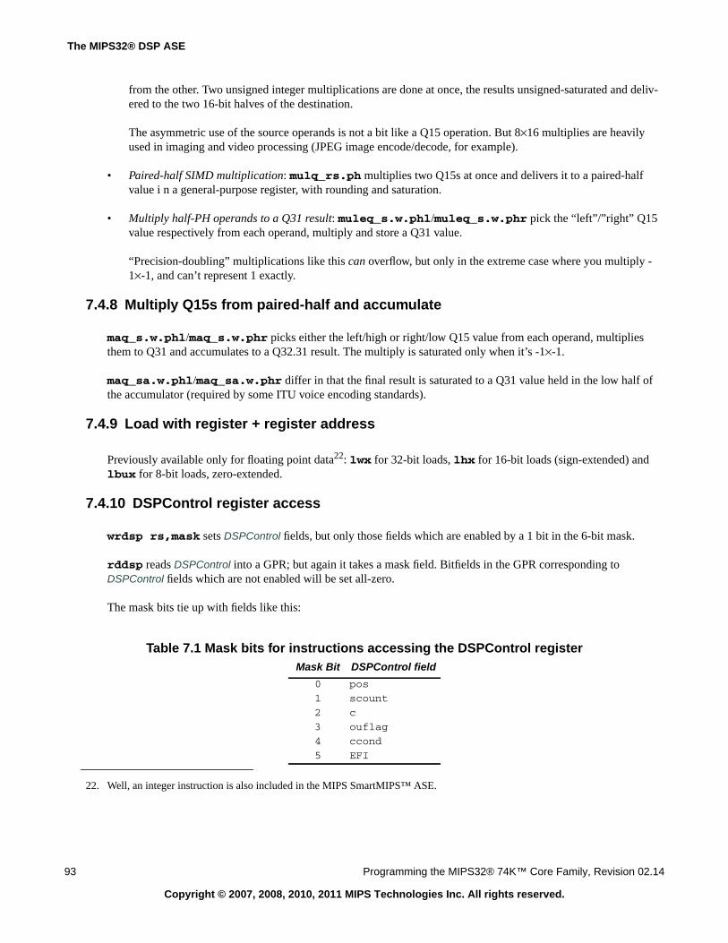
The MIPS32® DSP ASE
93 Programming the MIPS32® 74K™ Core Family, Revision 02.14
Copyright © 2007, 2008, 2010, 2011 MIPS Technologies Inc. All rights reserved.
from the other. Two unsigned integer multiplications are done at once, the results unsigned-saturated and deliv-ered to the two 16-bit halves of the destination.
The asymmetric use of the source operands is not a bit like a Q15 operation. But 8×16 multiplies are heavilyused in imaging and video processing (JPEG image encode/decode, for example).
• Paired-half SIMD multiplication: mulq_rs.ph multiplies two Q15s at once and delivers it to a paired-halfvalue i n a general-purpose register, with rounding and saturation.
• Multiply half-PH operands to a Q31 result: muleq_s.w.phl/muleq_s.w.phr pick the “left”/”right” Q15value respectively from each operand, multiply and store a Q31 value.
“Precision-doubling” multiplications like this can overflow, but only in the extreme case where you multiply -1×-1, and can’t represent 1 exactly.
7.4.8 Multiply Q15s from paired-half and accumulate
maq_s.w.phl/maq_s.w.phr picks either the left/high or right/low Q15 value from each operand, multipliesthem to Q31 and accumulates to a Q32.31 result. The multiply is saturated only when it’s -1×-1.
maq_sa.w.phl/maq_sa.w.phr differ in that the final result is saturated to a Q31 value held in the low half ofthe accumulator (required by some ITU voice encoding standards).
7.4.9 Load with register + register address
Previously available only for floating point data22: lwx for 32-bit loads, lhx for 16-bit loads (sign-extended) andlbux for 8-bit loads, zero-extended.
7.4.10 DSPControl register access
wrdsp rs,mask sets DSPControl fields, but only those fields which are enabled by a 1 bit in the 6-bit mask.
rddsp reads DSPControl into a GPR; but again it takes a mask field. Bitfields in the GPR corresponding toDSPControl fields which are not enabled will be set all-zero.
The mask bits tie up with fields like this:
22. Well, an integer instruction is also included in the MIPS SmartMIPS™ ASE.
Table 7.1 Mask bits for instructions accessing the DSPControl registerMask Bit DSPControl field
0 pos
1 scount
2 c
3 ouflag
4 ccond
5 EFI
7.4 DSP instructions
Programming the MIPS32® 74K™ Core Family, Revision 02.14 94
Copyright © 2007, 2008, 2010, 2011 MIPS Technologies Inc. All rights reserved.
7.4.11 Accumulator access instructions
• Historical instructions which now access new accumulators: the familiar mfhi/mflo/mthi/mtlo instructionsnow take an optional extra accumulator-number parameter.
• Shift and move to general register: extr.w/extr_r.w/extr_rs.w gets a 32-bit field from an accumulator(starting at bit 0 up to 31) and puts the value in a general purpose register. At your option you can specify round-ing and signed 32-bit saturation.
extrv.w/extrv_r.w/extrv_rs.w do the same but specify the field’s starting bit number with a register.
• Extract bitfield from accumulator: extp/extpv takes a bitfield (up to 32 bits) from an accumulator and movesit to a GPR. The length of the field can be an immediate value or from a register. The position of the field is deter-mined by DSPControl[pos], which holds the bit number of the most significant bit.
extpdp/extpdpv do the same, but also auto-decrement DSPControl[pos] to the bit-number just below the fieldyou extracted.
• Accumulator rearrangement: shilo/shilov has a signed shift value between -32 and +31, where positivenumbers shift right, and negative ones shift left. The “v” version, as usual, takes the shift value from a register.The right shift is a “logical” type so the result is zero extended.
• Fill accumulator pushing low half to high: mthlip moves the low half of the accumulator to the high half, thenwrites the GPR value in the low half. Generally used to bring 32 more bits from a bitstream into the accumulatorfor parsing by the various ext... instructions.
7.4.12 Dot products and building blocks for complex multiplication
In 2-dimensional vector math (or in any doubled-up step of a multiply-accumulate sequence which has been opti-mized for 2-way SIMD) you’re often interested in the dot product of two vectors:
v[0]*w[0] + v[1]*w[1]
In many cases you take the dot product of a series of vectors and add it up, too.
Some algorithms use complex numbers, represented by 2D vectors. Complex numbers use i to stand for “the squareroot of -1”, and a vector [a,b] is interpreted as a+ib (mathematicians leave out the multiply sign and use single-letter variables, habits which would not be appreciated in C programming!) Complex multiplication just follows therules of multiplying out sums, remembering that i*i=-1, so:
(a + ib)*(c + id) = (a*c - b*d) + i(a*d + b*c)
Or in vector format:
[a, b] * [c, d] = [a*c - b*d, a*d + b*c]
The first element of the result (the “real component”) is like a dot product but with a subtraction, and the second (the“imaginary component”) is like a dot product but with the vectors crossed.
The MIPS32® DSP ASE
95 Programming the MIPS32® 74K™ Core Family, Revision 02.14
Copyright © 2007, 2008, 2010, 2011 MIPS Technologies Inc. All rights reserved.
• Q15 dot product from paired-half, and accumulate: dpaq_s.w.ph does a SIMD multiply of the Q15 halves ofthe operands, then adds the results and saturates to form a Q31 fraction, which is accumulated into a Q32.31 frac-tion in the accumulator.
dpsq_s.w.ph does the same but subtracts the dot product from the accumulator.
For the imaginary component of a complex multiply, first swap the Q15 numbers in one of the register operandswith a rot (bit-rotate) instruction.
For the real component of a complex Q15 multiply, you have the difference-of-products instructionmulsaq_s.w.ph, which parallel-multiplies both Q15 halves of the PH operands, then computes the differenceof the two results and leaves it in an accumulator in Q32.31 format (beware: this does not accumulate the result).
• 16-bit integer dot-product from paired-half, and accumulate: dpau.h.qbl/dpau.h.qbr picks two QB val-ues from each source register, parallel-multiplies the corresponding pairs to integer 16-bit values, adds themtogether and then adds the whole lot into an accumulator. dpsu.h.qbl/dpsu.h.qbr do the same sum-of-products, but the result is then subtracted from the accumulator. In both cases, note this is integer (not fractional)arithmetic.
• Q31 saturated multiply-accumulate: is the nearest thing you can get to a dot-product for Q31 values.dpaq_sa.l.w does a Q31 multiplication and saturates to produce a Q63 result, which is added to the accumu-lator and saturated again. dpsq_sa.l.w does the same, except that the multiply result is subtracted from theaccumulator (again, useful for the real component of a complex number).
7.4.13 Other DSP ASE instructions
• Branch on DSPControl field: bposge32 branches if DSPControl[pos]≥32.
Typically the test is for “is it time to load another 32 bits of data from the bitstream yet?”.
• Circular buffer index update: modsub takes an operand which packs both a maximum index value and an indexstep, and uses it to decrement a “buffer index” by the step value, but arranging to step from zero to the providedmaximum.
• Bitfield insert with variable size/position: insv is a bit-insert instruction. It acts like the MIPS32 standardinstruction ins except that the position and size of the inserted field are specified not as immediates inside theinstruction, but are obtained from DSPControl[pos] (which should be set to the lowest numbered bit of the fieldyou want) and DSPControl[scount] respectively.
• Bit-order reversal: bitrev reverses the bits in the low 16 bits of the register. The high half of the destination iszero.
The bit-reverse operation is a computationally crucial step in buffer management for FFT algorithms, and a 16-bit operation supports up to a 32K-point FFT, which is much more than enough. A full 32-bit reversal would beexpensive and slow.
7.5 Macros and typedefs for DSP instructions
It’s useful to be able to use fragments of C code to describe what some instructions do. To do that, we need to be able
to refer to fractional types, saturation and vectors. Here are the definitions we’re using23:
7.6 Almost Alphabetically-ordered table of DSP ASE instructions
Programming the MIPS32® 74K™ Core Family, Revision 02.14 96
Copyright © 2007, 2008, 2010, 2011 MIPS Technologies Inc. All rights reserved.
typedef long long int64;typedef int int32;
/* accumulator type */typedef signed long long q32_31;
typedef signed int q31;
#define MAX31 0x7FFFFFFF#define MIN31 -(1<<31)#define SAT31(x) (x > MAX31 ? MAX31: x < MIN31 ? MIN31: x)
typedef signed short q15;#define MAX15 0x7FFF#define MIN15 -(1<<15)#define SAT15(x) (x > MAX15 ? MAX15: x < MIN15 ? MIN15: x)
typedef unsigned char u8;#define MAXUBYTE 255#define SATUBYTE(x) (x > MAXUBYTE ? MAXUBYTE: x < 0 ? 0: x)
/* fields in the vector types are specified by relative bit position, but C definitions are in memory order, so these definitions need to be endianness-dependent */
#ifdef BIG_ENDIANtypedef struct{ q15 h1, h0;} ph;
typedef struct{ u8 b3, b2, b1, b0;} qb;#elsetypedef struct{ q15 h0, h1;} ph;
typedef struct{ u8 b0, b1, b2, b3;} qb;#endif
7.6 Almost Alphabetically-ordered table of DSP ASE instructions
23. This page needs more work, and I hope it will be improved in a future version of the manual.
Table 7.2 DSP instructions in alphabetical orderInstruction Description
absq_s.w rd,rt Q31/signed integer absolute value with saturationaddq.ph rd,rs,rt 2×SIMD Q15 addition, without and with saturation of the resultaddq_s.ph rd,rs,rt
addq_s.w rd,rs,rt Q31/signed integer addition with saturation
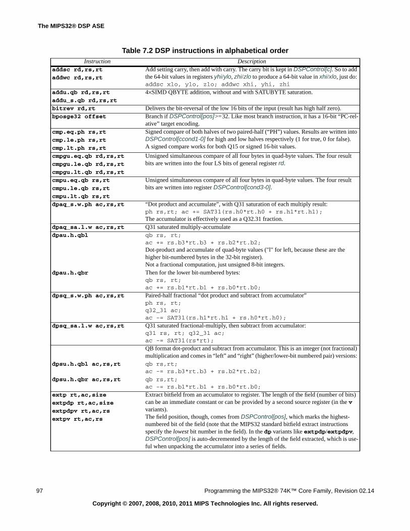
The MIPS32® DSP ASE
97 Programming the MIPS32® 74K™ Core Family, Revision 02.14
Copyright © 2007, 2008, 2010, 2011 MIPS Technologies Inc. All rights reserved.
addsc rd,rs,rt Add setting carry, then add with carry. The carry bit is kept in DSPControl[c]. So to addthe 64-bit values in registers yhi/ylo, zhi/zlo to produce a 64-bit value in xhi/xlo, just do:addsc xlo, ylo, zlo; addwc xhi, yhi, zhi
addwc rd,rs,rt
addu.qb rd,rs,rt 4×SIMD QBYTE addition, without and with SATUBYTE saturation.addu_s.qb rd,rs,rt
bitrev rd,rt Delivers the bit-reversal of the low 16 bits of the input (result has high half zero).bposge32 offset Branch if DSPControl[pos]>=32. Like most branch instruction, it has a 16-bit “PC-rel-
ative” target encoding.cmp.eq.ph rs,rt Signed compare of both halves of two paired-half (“PH”) values. Results are written into
DSPControl[ccond1-0] for high and low halves respectively (1 for true, 0 for false).A signed compare works for both Q15 or signed 16-bit values.
cmp.le.ph rs,rt
cmp.lt.ph rs,rt
cmpgu.eq.qb rd,rs,rt Unsigned simultaneous compare of all four bytes in quad-byte values. The four resultbits are written into the four LS bits of general register rd.cmpgu.le.qb rd,rs,rt
cmpgu.lt.qb rd,rs,rt
cmpu.eq.qb rs,rt Unsigned simultaneous compare of all four bytes in quad-byte values. The four resultbits are written into register DSPControl[cond3-0].cmpu.le.qb rs,rt
cmpu.lt.qb rs,rt
dpaq_s.w.ph ac,rs,rt “Dot product and accumulate”, with Q31 saturation of each multiply result:ph rs,rt; ac += SAT31(rs.h0*rt.h0 + rs.h1*rt.h1);The accumulator is effectively used as a Q32.31 fraction.
dpaq_sa.l.w ac,rs,rt Q31 saturated multiply-accumulatedpau.h.qbl qb rs, rt;
ac += rs.b3*rt.b3 + rs.b2*rt.b2;Dot-product and accumulate of quad-byte values ("l" for left, because these are thehigher bit-numbered bytes in the 32-bit register).Not a fractional computation, just unsigned 8-bit integers.
dpau.h.qbr Then for the lower bit-numbered bytes:qb rs, rt;ac += rs.b1*rt.b1 + rs.b0*rt.b0;
dpsq_s.w.ph ac,rs,rt Paired-half fractional “dot product and subtract from accumulator”ph rs, rt;q32_31 ac;ac -= SAT31(rs.h1*rt.h1 + rs.h0*rt.h0);
dpsq_sa.l.w ac,rs,rt Q31 saturated fractional-multiply, then subtract from accumulator:q31 rs, rt; q32_31 ac;ac -= SAT31(rs*rt);
QB format dot-product and subtract from accumulator. This is an integer (not fractional)multiplication and comes in “left” and “right” (higher/lower-bit numbered pair) versions:
dpsu.h.qbl ac,rs,rt qb rs,rt;ac -= rs.b3*rt.b3 + rs.b2*rt.b2;
dpsu.h.qbr ac,rs,rt qb rs,rt;ac -= rs.b1*rt.b1 + rs.b0*rt.b0;
extp rt,ac,size Extract bitfield from an accumulator to register. The length of the field (number of bits)can be an immediate constant or can be provided by a second source register (in the vvariants).The field position, though, comes from DSPControl[pos], which marks the highest-numbered bit of the field (note that the MIPS32 standard bitfield extract instructionsspecify the lowest bit number in the field). In the dp variants like extpdp/extpdpv,DSPControl[pos] is auto-decremented by the length of the field extracted, which is use-ful when unpacking the accumulator into a series of fields.
extpdp rt,ac,size
extpdpv rt,ac,rs
extpv rt,ac,rs
Table 7.2 DSP instructions in alphabetical orderInstruction Description
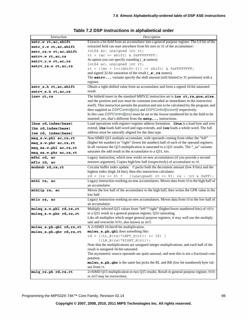
7.6 Almost Alphabetically-ordered table of DSP ASE instructions
Programming the MIPS32® 74K™ Core Family, Revision 02.14 98
Copyright © 2007, 2008, 2010, 2011 MIPS Technologies Inc. All rights reserved.
extr.w rt,ac,shift Extracts a bit field from an accumulator into a general purpose register. The LS bit of theextracted field can start anywhere from bit zero to 31 of the accumulator:int64 ac; unsigned int rt;rt = (ac >> shift) & 0xFFFFFFFF;At option you can specify rounding (_r names):int64 ac; unsigned int rt;rt = ((ac + 1<<(shift-1)) >> shift) & 0xFFFFFFFF;and signed 32-bit saturation of the result (_s/_rs names).The extrv... variants specify the shift amount (still limited to 31 positions) with aregister.
extr_r.w rt,ac,shift
extr_rs.w rt,ac,shift
extrv.w rt,ac,rs
extrv_r.w rt,ac,rs
extrv_rs.w rt,ac,rs
extr_s.h rt,ac,shift Obtain a right-shifted value from an accumulator and form a signed 16-bit saturatedresult.extrv_s.h rt,ac,rs
insv rt,rs The bitfield insert in the standard MIPS32 instruction set is ins rt,rs,pos,size,and the position and size must be constants (encoded as immediates in the instructionitself). This instruction permits the position and size to be calculated by the program, andthen supplied as DSPControl[pos] and DSPControl[scount] respectively.In this case DSPControl[pos] must be set to the lowest numbered bit in the field to beinserted: yes, that’s different from the extp... instructions.
lbux rd,index(base) Load operations with register+register address formation. lbux is a load byte and zeroextend, lhx loads half-word and sign-extends, and lwx loads a whole word. The fulladdress must be naturally aligned for the data type.
lhx rd,index(base)
lwx rd, index(base)
maq_s.w.phl ac,rs,rt Non-SIMD Q15 multiply-accumulate, with operands coming from either the “left”(higher bit number) or “right” (lower bit number) half of each of the operand registers.In all versions the Q15 multiplication is saturated to a Q31 results. The “_sa” variantssaturates the add result in the accumulator to a Q31, too.
maq_s.w.phr ac,rs,rt
maq_sa.w.phl ac,rs,rt
maq_sa.w.phr ac,rs,rt
mfhi rd, ac Legacy instruction, which now works on new accumulators (if you provide a secondnonzero argument). Copies high/low half (respectively) of accumulator to rd.mflo rd, ac
modsub rd,rs,rt Circular buffer index update. rt packs both the decrement amount (low 8 bits) and thehighest index (high 24 bits), then this instruction calculates:rd = (rs == 0) ? ((unsigned) rt >> 8): rs - (rt & 0xFF);
mthi rs, ac Legacy instruction working on new accumulators. Moves data from rd to the high half ofan accumulator.
mthlip rs, ac Moves the low half of the accumulator to the high half, then writes the GPR value in thelow half.
mtlo rs, ac Legacy instruction working on new accumulators. Moves data from rd to the low half ofan accumulator.
muleq_s.w.phl rd,rs,rt Multiply selected Q15 values from “left”/“right” (higher/lower numbered bits) of rd/rsto a Q31 result in a general purpose register, Q31-saturating.Like all multiplies which target general purpose registers, it may well use the multiplyunit and overwrite hi/lo, also known as ac0.
muleq_s.w.phr rd,rs,rt
muleu_s.ph.qbl rd,rs,rt A 2×SIMD 16-bit×8-bit multiplication.muleu_s.ph.qbl does something like:rd = ((LL_B(rs)*LEFT_H(rt)) << 16) | ((LR_B(rs)*RIGHT_H(rt));Note that the multiplications are unsigned integer multiplications, and each half of theresult is unsigned-16-bit-saturated.The asymmetric source operands are quite unusual, and note this is not a fractional com-putation.muleu_s.ph.qbr is the same but picks the RL and RR (low bit numbered) byte val-ues from rs.
muleu_s.ph.qbr rd,rs,rt
mulq_rs.ph rd,rs,rt 2×SIMD Q15 multiplication to two Q15 results. Result in general purpose register, hi/loor ac0 may be overwritten.
Table 7.2 DSP instructions in alphabetical orderInstruction Description
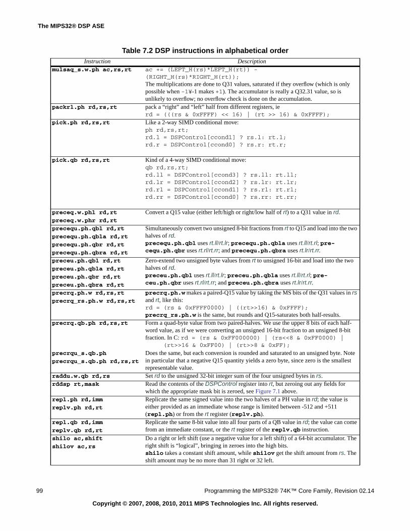
The MIPS32® DSP ASE
99 Programming the MIPS32® 74K™ Core Family, Revision 02.14
Copyright © 2007, 2008, 2010, 2011 MIPS Technologies Inc. All rights reserved.
mulsaq_s.w.ph ac,rs,rt ac += (LEFT_H(rs)*LEFT_H(rt)) -(RIGHT_H(rs)*RIGHT_H(rt));The multiplications are done to Q31 values, saturated if they overflow (which is onlypossible when -1¥-1 makes +1). The accumulator is really a Q32.31 value, so isunlikely to overflow; no overflow check is done on the accumulation.
packrl.ph rd,rs,rt pack a “right” and “left” half from different registers, ierd = (((rs & 0xFFFF) << 16) | (rt >> 16) & 0xFFFF);
pick.ph rd,rs,rt Like a 2-way SIMD conditional move:ph rd,rs,rt;rd.l = DSPControl[ccond1] ? rs.l: rt.l;rd.r = DSPControl[ccond0] ? rs.r: rt.r;
pick.qb rd,rs,rt Kind of a 4-way SIMD conditional move:qb rd,rs,rt;rd.ll = DSPControl[ccond3] ? rs.ll: rt.ll;rd.lr = DSPControl[ccond2] ? rs.lr: rt.lr;rd.rl = DSPControl[ccond1] ? rs.rl: rt.rl;rd.rr = DSPControl[ccond0] ? rs.rr: rt.rr;
preceq.w.phl rd,rt Convert a Q15 value (either left/high or right/low half of rt) to a Q31 value in rd.preceq.w.phr rd,rt
precequ.ph.qbl rd,rt Simultaneously convert two unsigned 8-bit fractions from rt to Q15 and load into the twohalves of rd.precequ.ph.qbl uses rt.ll/rt.lr; precequ.ph.qbla uses rt.ll/rt.rl; pre-cequ.ph.qbr uses rt.rl/rt.rr; and precequ.ph.qbra uses rt.lr/rt.rr.
precequ.ph.qbla rd,rt
precequ.ph.qbr rd,rt
precequ.ph.qbra rd,rt
preceu.ph.qbl rd,rt Zero-extend two unsigned byte values from rt to unsigned 16-bit and load into the twohalves of rd.preceu.ph.qbl uses rt.ll/rt.lr; preceu.ph.qbla uses rt.ll/rt.rl; pre-ceu.ph.qbr uses rt.rl/rt.rr; and preceu.ph.qbra uses rt.lr/rt.rr.
preceu.ph.qbla rd,rt
preceu.ph.qbr rd,rt
preceu.ph.qbra rd,rt
precrq.ph.w rd,rs,rt precrq.ph.w makes a paired-Q15 value by taking the MS bits of the Q31 values in rsand rt, like this:rd = (rs & 0xFFFF0000) | ((rt>>16) & 0xFFFF);precrq_rs.ph.w is the same, but rounds and Q15-saturates both half-results.
precrq_rs.ph.w rd,rs,rt
precrq.qb.ph rd,rs,rt Form a quad-byte value from two paired-halves. We use the upper 8 bits of each half-word value, as if we were converting an unsigned 16-bit fraction to an unsigned 8-bitfraction. In C: rd = (rs & 0xFF000000) | (rs<<8 & 0xFF0000) | (rt>>16 & 0xFF00) | (rt>>8 & 0xFF);
precrqu_s.qb.ph Does the same, but each conversion is rounded and saturated to an unsigned byte. Notein particular that a negative Q15 quantity yields a zero byte, since zero is the smallestrepresentable value.
precrqu_s.qb.ph rd,rs,rt
raddu.w.qb rd,rs Set rd to the unsigned 32-bit integer sum of the four unsigned bytes in rs.rddsp rt,mask Read the contents of the DSPControl register into rt, but zeroing out any fields for
which the appropriate mask bit is zeroed, see Figure 7.1 above.repl.ph rd,imm Replicate the same signed value into the two halves of a PH value in rd; the value is
either provided as an immediate whose range is limited between -512 and +511(repl.ph) or from the rt register (replv.ph).
replv.ph rd,rt
repl.qb rd,imm Replicate the same 8-bit value into all four parts of a QB value in rd; the value can comefrom an immediate constant, or the rt register of the replv.qb instruction.replv.qb rd,rt
shilo ac,shift Do a right or left shift (use a negative value for a left shift) of a 64-bit accumulator. Theright shift is “logical”, bringing in zeroes into the high bits.shilo takes a constant shift amount, while shilov get the shift amount from rs. Theshift amount may be no more than 31 right or 32 left.
shilov ac,rs
Table 7.2 DSP instructions in alphabetical orderInstruction Description
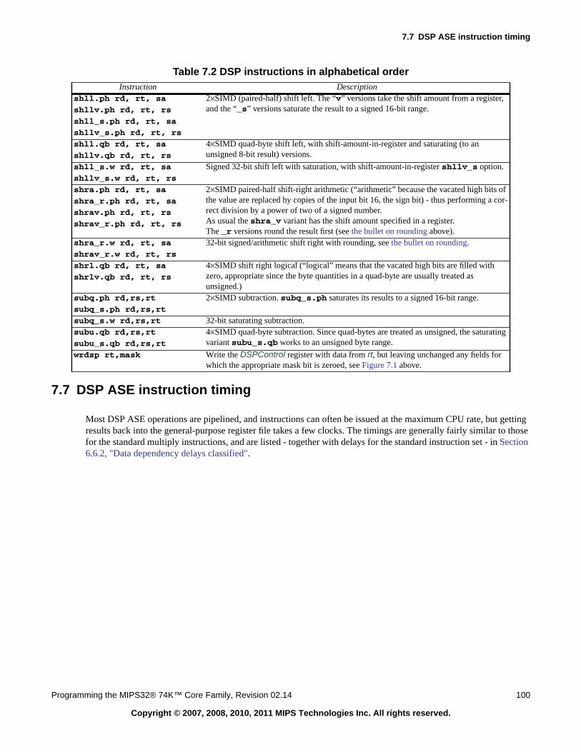
7.7 DSP ASE instruction timing
Programming the MIPS32® 74K™ Core Family, Revision 02.14 100
Copyright © 2007, 2008, 2010, 2011 MIPS Technologies Inc. All rights reserved.
7.7 DSP ASE instruction timing
Most DSP ASE operations are pipelined, and instructions can often be issued at the maximum CPU rate, but gettingresults back into the general-purpose register file takes a few clocks. The timings are generally fairly similar to thosefor the standard multiply instructions, and are listed - together with delays for the standard instruction set - in Section6.6.2, "Data dependency delays classified".
shll.ph rd, rt, sa 2×SIMD (paired-half) shift left. The “v” versions take the shift amount from a register,and the “_s” versions saturate the result to a signed 16-bit range.shllv.ph rd, rt, rs
shll_s.ph rd, rt, sa
shllv_s.ph rd, rt, rs
shll.qb rd, rt, sa 4×SIMD quad-byte shift left, with shift-amount-in-register and saturating (to anunsigned 8-bit result) versions.shllv.qb rd, rt, rs
shll_s.w rd, rt, sa Signed 32-bit shift left with saturation, with shift-amount-in-register shllv_s option.shllv_s.w rd, rt, rs
shra.ph rd, rt, sa 2×SIMD paired-half shift-right arithmetic (“arithmetic” because the vacated high bits ofthe value are replaced by copies of the input bit 16, the sign bit) - thus performing a cor-rect division by a power of two of a signed number.As usual the shra_v variant has the shift amount specified in a register.The _r versions round the result first (see the bullet on rounding above).
shra_r.ph rd, rt, sa
shrav.ph rd, rt, rs
shrav_r.ph rd, rt, rs
shra_r.w rd, rt, sa 32-bit signed/arithmetic shift right with rounding, see the bullet on rounding.shrav_r.w rd, rt, rs
shrl.qb rd, rt, sa 4×SIMD shift right logical (“logical” means that the vacated high bits are filled withzero, appropriate since the byte quantities in a quad-byte are usually treated asunsigned.)
shrlv.qb rd, rt, rs
subq.ph rd,rs,rt 2×SIMD subtraction. subq_s.ph saturates its results to a signed 16-bit range.subq_s.ph rd,rs,rt
subq_s.w rd,rs,rt 32-bit saturating subtraction.subu.qb rd,rs,rt 4×SIMD quad-byte subtraction. Since quad-bytes are treated as unsigned, the saturating
variant subu_s.qb works to an unsigned byte range.subu_s.qb rd,rs,rt
wrdsp rt,mask Write the DSPControl register with data from rt, but leaving unchanged any fields forwhich the appropriate mask bit is zeroed, see Figure 7.1 above.
Table 7.2 DSP instructions in alphabetical orderInstruction Description
The MIPS32® DSP ASE
101 Programming the MIPS32® 74K™ Core Family, Revision 02.14
Copyright © 2007, 2008, 2010, 2011 MIPS Technologies Inc. All rights reserved.
Chapter 8
Programming the MIPS32® 74K™ Core Family, Revision 02.14 102
Copyright © 2007, 2008, 2010, 2011 MIPS Technologies Inc. All rights reserved.
74K™ core features for debug and profiling
In this chapter you’ll find:
• Section 8.1, "EJTAG on-chip debug unit"
• Section 8.3, "CP0 Watchpoints" - monitor code and data access without using EJTAG.
• Section 8.4, "Performance counters" - gather statistics about events, useful for understanding where your pro-gram spends its time.
The description here is terse and leaves out some information about EJTAG and PDtrace facilities which are not visi-ble to programmers. We will document it here if it’s software visible, or is implementation-dependent information notfound in the detailed documentation (see [EJTAG],).
8.1 EJTAG on-chip debug unit
This is a collection of in-CPU resources to support debug. Debug logic serves no direct purpose in the final end-userapplication, so it’s always under threat of being omitted for cost reasons. A debug unit must have virtually no perfor-mance impact when not in use; it must use few or no dedicated package pins, and should not increase the logic gatecount too much. EJTAG solves the pin issue (and gets its name) by recycling the JTAG pins already included in every
SoC for chip test24.
So the debug unit requires:
• Physical communications with some kind of “probe” device (which is itself controlled by the debug host),achieved through the JTAG pins.
• The ability for a probe to “remote-control” the CPU. The basic trick is to get the CPU to execute instructions thatthe probe supplies. In turn that’s done by directing the CPU to execute code from the magic “dmseg” regionwhere CPU reads and writes are made down the wire to the probe. “dmseg” is itself a part of “dseg”, see Section8.1.5, "The “dseg” memory decode region".
• A distinguished debug exception. In MIPS EJTAG, this is a special “super-exception” marked by a specialdebug-exception-level flag, so you can use an EJTAG debugger even on regular exception handler code. SeeSection 8.1.2, "Debug mode" below;
• A number of “hardware breakpoints”. Their numerous control registers can’t be accommodated in the CP0 regis-ter set, so are memory-mapped into “dseg”;
• You can take a debug exception from a special breakpoint instruction sdbbp, on a match from an EJTAG hard-ware breakpoint, after an EJTAG single-step, when the probe writes the break bit EJTAG_CONTROL[EjtagBrk],or by asserting the external DINT (debug interrupt) signal.
24. It can actually be quite useful to provide EJTAG with its own pins, if your package permits.
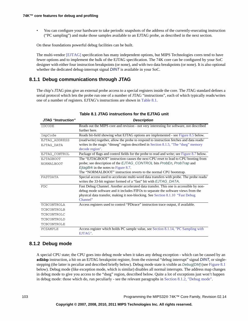
74K™ core features for debug and profiling
103 Programming the MIPS32® 74K™ Core Family, Revision 02.14
Copyright © 2007, 2008, 2010, 2011 MIPS Technologies Inc. All rights reserved.
• You can configure your hardware to take periodic snapshots of the address of the currently-executing instruction(“PC sampling”) and make those samples available to an EJTAG probe, as described in the next section.
On these foundations powerful debug facilities can be built.
The multi-vendor [EJTAG] specification has many independent options, but MIPS Technologies cores tend to havefewer options and to implement the bulk of the EJTAG specification. The 74K core can be configured by your SoCdesigner with either four instruction breakpoints (or none), and with two data breakpoints (or none). It is also optionalwhether the dedicated debug-interrupt signal DINT is available in your SoC.
8.1.1 Debug communications through JTAG
The chip’s JTAG pins give an external probe access to a special registers inside the core. The JTAG standard defines aserial protocol which lets the probe run one of a number of JTAG “instructions”, each of which typically reads/writesone of a number of registers. EJTAG’s instructions are shown in Table 8.1.
8.1.2 Debug mode
A special CPU state; the CPU goes into debug mode when it takes any debug exception - which can be caused by ansdbbp instruction, a hit on an EJTAG breakpoint register, from the external “debug interrupt” signal DINT, or single-stepping (the latter is peculiar and described briefly below). Debug mode state is visible as Debug[DM] (see Figure 8.1below). Debug mode (like exception mode, which is similar) disables all normal interrupts. The address map changesin debug mode to give you access to the “dseg” region, described below. Quite a lot of exceptions just won’t happenin debug mode: those which do, run peculiarly - see the relevant paragraphs in Section 8.1.2, "Debug mode".
Table 8.1 JTAG instructions for the EJTAG unitJTAG “Instruction” Description
IDCODE Reads out the MIPS core and revision - not very interesting for software, not describedfurther here.
ImpCode Reads bit-field showing what EJTAG options are implemented - see Figure 8.5 below.EJTAG_ADDRESS (read/write) together, allow the probe to respond to instruction fetches and data reads/
writes in the magic “dmseg” region described in Section 8.1.5, "The “dseg” memorydecode region".
EJTAG_DATA
EJTAG_CONTROL Package of flags and control fields for the probe to read and write; see Figure 8.7 below.EJTAGBOOT The “EJTAGBOOT” instruction causes the next CPU reset to lead to CPU booting from
probe; see description of the EJTAG_CONTROL bits ProbEn, ProbTrap andEjtagBrk in the notes to Figure 8.7.The “NORMALBOOT” instruction reverts to the normal CPU bootstrap.
NORMALBOOT
FASTDATA Special access used to accelerate multi-word data transfers with probe. The probe reads/writes the 33-bit register formed of a “fast” bit with EJTAG_DATA.
FDC Fast Debug Channel. Another accelerated data transfer. This one is accessible by non-debug mode software and it includes FIFOs to separate the software views from thephysical data transfer, making it non-blocking. See Section 8.1.10 “Fast DebugChannel”
TCBCONTROLA Access registers used to control “PDtrace” instruction trace output, if available.TCBCONTROLB
TCBCONTROLC
TCBCONTROLD
TCBCONTROLE
PCSAMPLE Access register which holds PC sample value, see Section 8.1.14, "PC Sampling withEJTAG".
8.1 EJTAG on-chip debug unit
Programming the MIPS32® 74K™ Core Family, Revision 02.14 104
Copyright © 2007, 2008, 2010, 2011 MIPS Technologies Inc. All rights reserved.
A CPU with a suitable probe attached can be set up so the debug exception entry point is in the “dmseg” region, run-ning instructions provided by the probe itself. With no probe attached, the debug exception entry point is in the ROMor potentially from an alternate memory location - see Table 5.1.
8.1.3 Exceptions in debug mode
Software debuggers will probably be coded to avoid causing exceptions (testing addresses in software, for example,rather than risking address or TLB exceptions).
While executing in debug mode many conditions which would normally cause an exception are ignored: interrupts,debug exceptions (other than that caused by executing sdbbp), and CP0 watchpoint hits.
But other exceptions are turned into “nested debug exceptions” when the CPU is in debug mode - a facility which isprobably mostly valuable to debuggers using the EJTAG probe.
On such a nested debug exception the CPU jumps to the debug exception entry point, remaining in debug mode. TheDebug[DExcCode] field records the cause of the nested exception, and DEPC records the debug-mode-code restartaddress. This will not be survivable for the debugger unless it saved a copy of the original DEPC soon after enteringdebug mode, but it probably did that! To return from a nested debug exception like this you don’t use deret (whichwould inappropriately take you out of debug mode), you grab the address out of DEPC and use a jump-register.
8.1.4 Single-stepping
When control returns from debug mode with a deret and the single-step bit Debug[SSt] is set, the instruction
selected by DEPC will be executed in non-debug context25; then a debug exception will be taken on the program’svery next instruction in sequence.
Since at least one instruction is run in normal mode it can lead to a non-debug exception; in that case the “very nextinstruction in sequence” will be the first instruction of the exception handler, and you’ll get a single-step debugexception whose DEPC points at the exception handler.
8.1.5 The “dseg” memory decode region
EJTAG needs to use memory space both to accommodate lots of breakpoint registers (too many for CP0) and for itsprobe-mapped communication space. This memory space pops into existence at the top of the CPU’s virtual addressmap when the CPU is in debug mode, as shown in Table 8.2.
The MIPS trace solution provides software the ability to access the on-chip trace memory. The TCB Registers aremapped to drseg space and this allows software to directly access the on-chip trace memory using load and storeinstructions.
25. If DEPC points to a branch instruction, both the branch and branch-delay instruction will be executed normally.
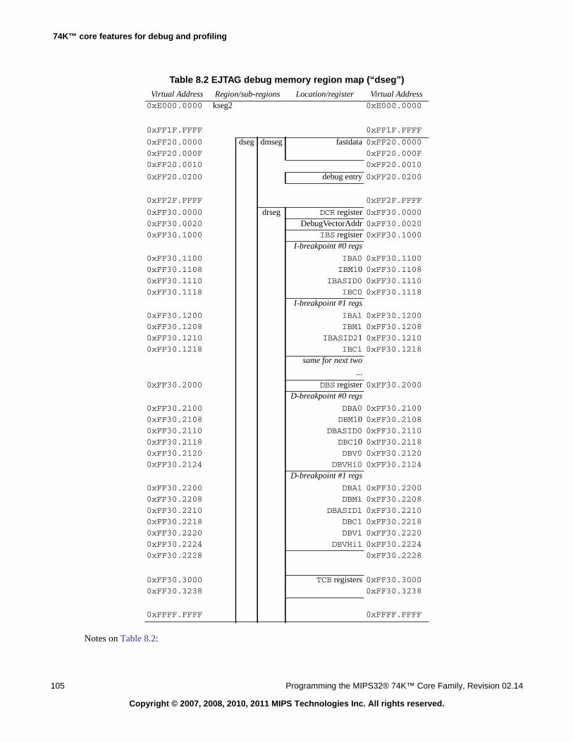
74K™ core features for debug and profiling
105 Programming the MIPS32® 74K™ Core Family, Revision 02.14
Copyright © 2007, 2008, 2010, 2011 MIPS Technologies Inc. All rights reserved.
Notes on Table 8.2:
Table 8.2 EJTAG debug memory region map (“dseg”)Virtual Address Region/sub-regions Location/register Virtual Address0xE000.0000 kseg2 0xE000.0000
0xFF1F.FFFF 0xFF1F.FFFF
0xFF20.0000 dseg dmseg fastdata 0xFF20.0000
0xFF20.000F 0xFF20.000F
0xFF20.0010 0xFF20.0010
0xFF20.0200 debug entry 0xFF20.0200
0xFF2F.FFFF 0xFF2F.FFFF
0xFF30.0000 drseg DCR register 0xFF30.00000xFF30.0020 DebugVectorAddr 0xFF30.00200xFF30.1000 IBS register 0xFF30.1000
I-breakpoint #0 regs
0xFF30.1100 IBA0 0xFF30.1100
0xFF30.1108 IBM10 0xFF30.1108
0xFF30.1110 IBASID0 0xFF30.1110
0xFF30.1118 IBC0 0xFF30.1118
I-breakpoint #1 regs
0xFF30.1200 IBA1 0xFF30.1200
0xFF30.1208 IBM1 0xFF30.1208
0xFF30.1210 IBASID21 0xFF30.1210
0xFF30.1218 IBC1 0xFF30.1218
same for next two
...
0xFF30.2000 DBS register 0xFF30.2000D-breakpoint #0 regs
0xFF30.2100 DBA0 0xFF30.2100
0xFF30.2108 DBM10 0xFF30.2108
0xFF30.2110 DBASID0 0xFF30.2110
0xFF30.2118 DBC10 0xFF30.2118
0xFF30.2120 DBV0 0xFF30.2120
0xFF30.2124 DBVHi0 0xFF30.2124
D-breakpoint #1 regs
0xFF30.2200 DBA1 0xFF30.2200
0xFF30.2208 DBM1 0xFF30.2208
0xFF30.2210 DBASID1 0xFF30.2210
0xFF30.2218 DBC1 0xFF30.2218
0xFF30.2220 DBV1 0xFF30.2220
0xFF30.2224 DBVHi1 0xFF30.2224
0xFF30.2228 0xFF30.2228
0xFF30.3000 TCB registers 0xFF30.3000
0xFF30.3238 0xFF30.3238
0xFFFF.FFFF 0xFFFF.FFFF
8.1 EJTAG on-chip debug unit
Programming the MIPS32® 74K™ Core Family, Revision 02.14 106
Copyright © 2007, 2008, 2010, 2011 MIPS Technologies Inc. All rights reserved.
• dseg: is the whole debug-mode-only memory area.
It’s possible for debug-mode software to read the “kseg2”-mapped locations “underneath” by settingDebug[LSNM] (see Figure 8.1).
• dmseg: is the memory region where reads and writes are implemented by the probe. But if no active probe isplugged in, or if DCR[PE] is clear, then accesses here cause reads and writes to be handled like regular “kseg3”accesses.
• drseg: is where the debug unit’s main register banks are accessed. Accesses to “drseg” don’t go off core. Regis-ters in “drseg” are word-wide, and should be accessed only with 32-bit word-wide loads and stores.
• fast-talk: is a corner of “dmseg” where probe-mapped reads and writes use a more JTAG-efficient block-modeprobe protocol, reducing the amount of JTAG traffic and allowing for faster data transfer. There’s no details abouthow it’s done in this document, see [EJTAG].
• debug entry: is the debug exception entry point. Because it lies in “dmseg”, the debug code can be implementedwholly in probe memory, allowing you to debug a system which has no physical memory reserved for debug.
• TCB Registers : These are the PDtrace EJTag Registers. They are physically located in the PDtrace unit, andmanaged by the PDtrace unit. For software to access the on-chip trace memory, these registers are mapped todrseg.
8.1.6 EJTAG CP0 registers, particularly Debug
In normal circumstances (specifically, when not in debug mode), the only software-visible part of the debug unit is itsset of three CP0 registers:
• Debug which has configuration and control bits, and is detailed below;
• DEPC keeps the restart address from the last debug exception (automatically used by the deret instruction);
• DESAVE is a CP0 register which is just 32-bits of read/write space. It’s available for a debug exception handlerwhich needs to save the value of a first general-purpose register, so that it can use that register as an address baseto save all the others.
Debug is the most complicated and interesting. It has so many fields defined that we’ve taken them in three groups:debug exception cause bits in Figure 8.2, information about regular exceptions which want to happen but can’tbecause you’re in debug mode in Figure 8.3, and everything else. The "everything else" category includes the mostimportant fields and comes first, in Figure 8.1.
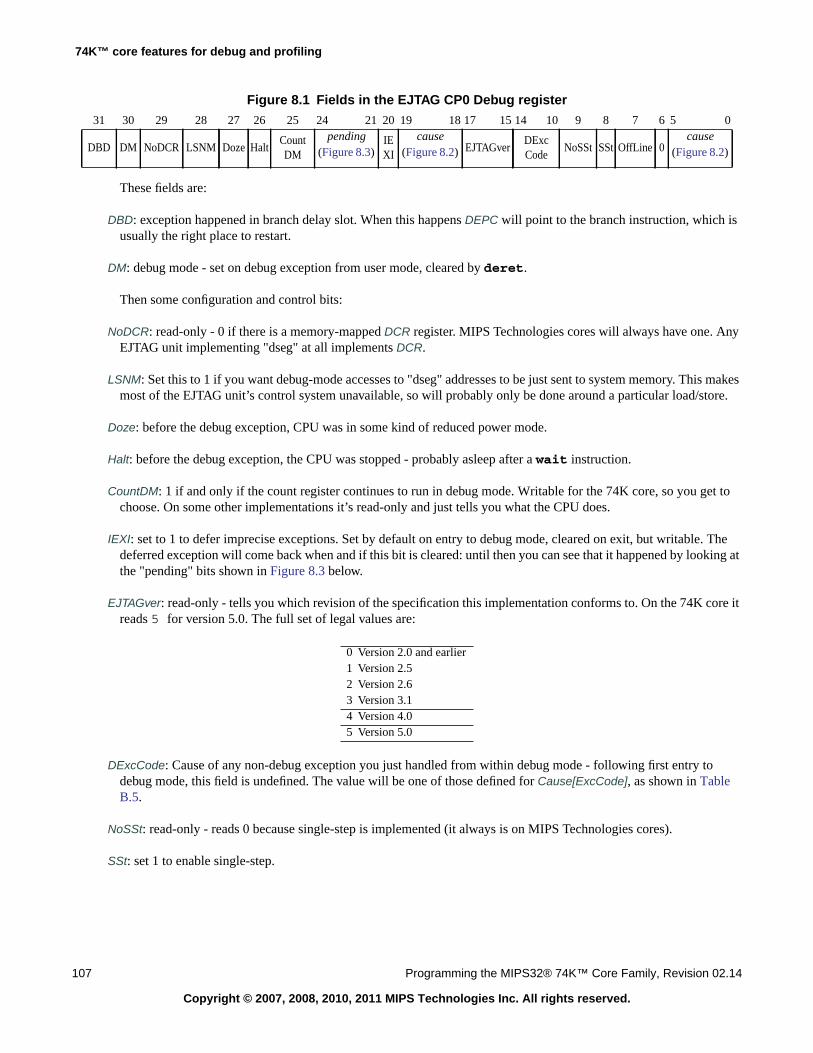
74K™ core features for debug and profiling
107 Programming the MIPS32® 74K™ Core Family, Revision 02.14
Copyright © 2007, 2008, 2010, 2011 MIPS Technologies Inc. All rights reserved.
These fields are:
DBD: exception happened in branch delay slot. When this happens DEPC will point to the branch instruction, which isusually the right place to restart.
DM: debug mode - set on debug exception from user mode, cleared by deret.
Then some configuration and control bits:
NoDCR: read-only - 0 if there is a memory-mapped DCR register. MIPS Technologies cores will always have one. AnyEJTAG unit implementing "dseg" at all implements DCR.
LSNM: Set this to 1 if you want debug-mode accesses to "dseg" addresses to be just sent to system memory. This makesmost of the EJTAG unit’s control system unavailable, so will probably only be done around a particular load/store.
Doze: before the debug exception, CPU was in some kind of reduced power mode.
Halt: before the debug exception, the CPU was stopped - probably asleep after a wait instruction.
CountDM: 1 if and only if the count register continues to run in debug mode. Writable for the 74K core, so you get tochoose. On some other implementations it’s read-only and just tells you what the CPU does.
IEXI: set to 1 to defer imprecise exceptions. Set by default on entry to debug mode, cleared on exit, but writable. Thedeferred exception will come back when and if this bit is cleared: until then you can see that it happened by looking atthe "pending" bits shown in Figure 8.3 below.
EJTAGver: read-only - tells you which revision of the specification this implementation conforms to. On the 74K core itreads 5 for version 5.0. The full set of legal values are:
DExcCode: Cause of any non-debug exception you just handled from within debug mode - following first entry todebug mode, this field is undefined. The value will be one of those defined for Cause[ExcCode], as shown in TableB.5.
NoSSt: read-only - reads 0 because single-step is implemented (it always is on MIPS Technologies cores).
SSt: set 1 to enable single-step.
Figure 8.1 Fields in the EJTAG CP0 Debug register31 30 29 28 27 26 25 24 21 20 19 18 17 15 14 10 9 8 7 6 5 0
DBD DM NoDCR LSNM Doze HaltCountDM
pending IEXI
causeEJTAGver
DExcCode
NoSSt SSt OffLine 0cause
(Figure 8.3) (Figure 8.2) (Figure 8.2)
0 Version 2.0 and earlier1 Version 2.52 Version 2.63 Version 3.14 Version 4.05 Version 5.0
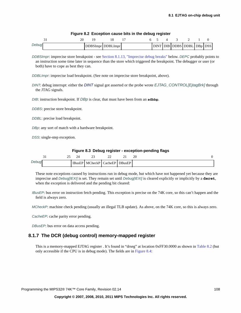
8.1 EJTAG on-chip debug unit
Programming the MIPS32® 74K™ Core Family, Revision 02.14 108
Copyright © 2007, 2008, 2010, 2011 MIPS Technologies Inc. All rights reserved.
DDBSImpr: imprecise store breakpoint - see Section 8.1.13, "Imprecise debug breaks" below. DEPC probably points toan instruction some time later in sequence than the store which triggered the breakpoint. The debugger or user (orboth) have to cope as best they can.
DDBLImpr: imprecise load breakpoint. (See note on imprecise store breakpoint, above).
DINT: debug interrupt: either the DINT signal got asserted or the probe wrote EJTAG_CONTROL[EjtagBrk] throughthe JTAG signals.
DIB: instruction breakpoint. If DBp is clear, that must have been from an sdbbp.
DDBS: precise store breakpoint.
DDBL: precise load breakpoint.
DBp: any sort of match with a hardware breakpoint.
DSS: single-step exception.
These note exceptions caused by instructions run in debug mode, but which have not happened yet because they areimprecise and Debug[IEXI] is set. They remain set until Debug[IEXI] is cleared explicitly or implicitly by a deret,when the exception is delivered and the pending bit cleared:
IBusEP: bus error on instruction fetch pending. This exception is precise on the 74K core, so this can’t happen and thefield is always zero.
MCheckP: machine check pending (usually an illegal TLB update). As above, on the 74K core, so this is always zero.
CacheEP: cache parity error pending.
DBusEP: bus error on data access pending.
8.1.7 The DCR (debug control) memory-mapped register
This is a memory-mapped EJTAG register . It’s found in “drseg” at location 0xFF30.0000 as shown in Table 8.2 (butonly accessible if the CPU is in debug mode). The fields are in Figure 8.4:
Figure 8.2 Exception cause bits in the debug register31 20 19 18 17 6 5 4 3 2 1 0
Debug DDBSImpr DDBLImpr DINT DIB DDBS DDBL DBp DSS
Figure 8.3 Debug register - exception-pending flags31 25 24 23 22 21 20 0
Debug IBusEP MCheckP CacheEP DBusEP
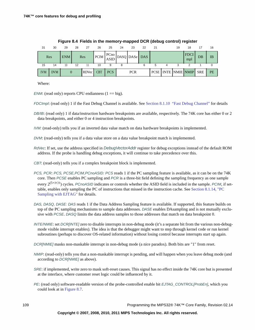
74K™ core features for debug and profiling
109 Programming the MIPS32® 74K™ Core Family, Revision 02.14
Copyright © 2007, 2008, 2010, 2011 MIPS Technologies Inc. All rights reserved.
Figure 8.4 Fields in the memory-mapped DCR (debug control) register
Where:
ENM: (read only) reports CPU endianness (1 == big).
FDCImpl: (read only) 1 if the Fast Debug Channel is available. See Section 8.1.10 “Fast Debug Channel” for details
DB/IB: (read only) 1 if data/instruction hardware breakpoints are available, respectively. The 74K core has either 0 or 2data breakpoints, and either 0 or 4 instruction breakpoints.
IVM: (read-only) tells you if an inverted data value match on data hardware breakpoints is implemented.
DVM: (read-only) tells you if a data value store on a data value breakpoint match is implemented.
RdVec: If set, use the address specified in DebugVectorAddr register for debug exceptions instead of the default ROMaddress. If the probe is handling debug exceptions, it will continue to take precedence over this.
CBT: (read-only) tells you if a complex breakpoint block is implemented.
PCS, PCR: PCS, PCSE,PCIM,PCnoASID: PCS reads 1 if the PC sampling feature is available, as it can be on the 74Kcore. Then PCSE enables PC sampling and PCR is a three-bit field defining the sampling frequency as one sample
every 2(5+PCR) cycles. PCnoASID indicates or controls whether the ASID field is included in the sample. PCIM, if set-table, enables only sampling the PC of instructions that missed in the instruction cache. See Section 8.1.14, "PCSampling with EJTAG" for details.
DAS, DASQ, DASE: DAS reads 1 if the Data Address Sampling feature is available. If supported, this feature builds ontop of the PC sampling mechanisms to sample data addresses. DASE enables DAsampling and is not mutually exclu-sive with PCSE. DASQ limits the data address samples to those addresses that match on data breakpoint 0.
INTE/NMIE: set DCR[INTE] zero to disable interrupts in non-debug mode (it’s a separate bit from the various non-debug-mode visible interrupt enables). The idea is that the debugger might want to step through kernel code or run kernelsubroutines (perhaps to discover OS-related information) without losing control because interrupts start up again.
DCR[NMIE] masks non-maskable interrupt in non-debug mode (a nice paradox). Both bits are "1" from reset.
NMIP: (read-only) tells you that a non-maskable interrupt is pending, and will happen when you leave debug mode (andaccording to DCR[NMIE] as above).
SRE: if implemented, write zero to mask soft-reset causes. This signal has no effect inside the 74K core but is presentedat the interface, where customer reset logic could be influenced by it.
PE: (read only) software-readable version of the probe-controlled enable bit EJTAG_CONTROL[ProbEn], which youcould look at in Figure 8.7.
31 30 29 28 27 26 25 24 23 22 21 19 18 17 16
Res ENM Res PCIMPCnoASID
DASQ DASe DASFDCImpl
DB IB
15 14 13 12 11 10 9 8 6 5 4 3 2 1 0
IVM DVM 0 RDVec CBT PCS PCR PCSE INTE NMIE NMIP SRE PE
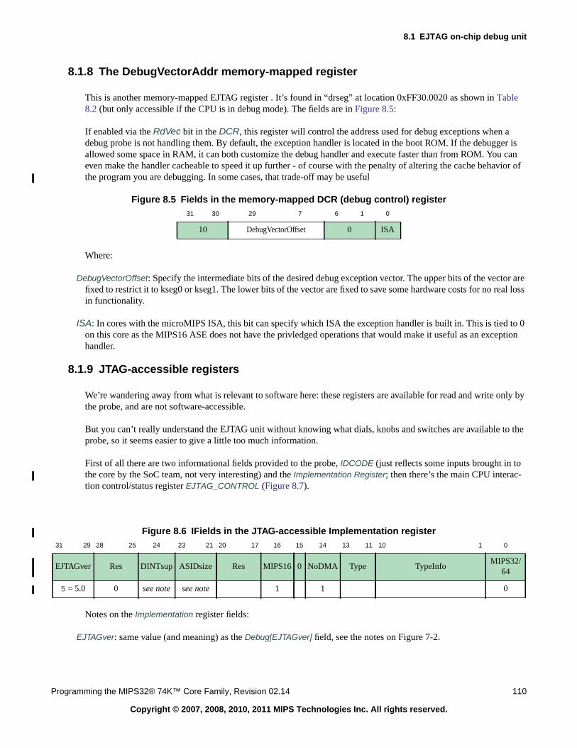
8.1 EJTAG on-chip debug unit
Programming the MIPS32® 74K™ Core Family, Revision 02.14 110
Copyright © 2007, 2008, 2010, 2011 MIPS Technologies Inc. All rights reserved.
8.1.8 The DebugVectorAddr memory-mapped register
This is another memory-mapped EJTAG register . It’s found in “drseg” at location 0xFF30.0020 as shown in Table8.2 (but only accessible if the CPU is in debug mode). The fields are in Figure 8.5:
If enabled via the RdVec bit in the DCR, this register will control the address used for debug exceptions when adebug probe is not handling them. By default, the exception handler is located in the boot ROM. If the debugger isallowed some space in RAM, it can both customize the debug handler and execute faster than from ROM. You caneven make the handler cacheable to speed it up further - of course with the penalty of altering the cache behavior ofthe program you are debugging. In some cases, that trade-off may be useful
Figure 8.5 Fields in the memory-mapped DCR (debug control) register
Where:
DebugVectorOffset: Specify the intermediate bits of the desired debug exception vector. The upper bits of the vector arefixed to restrict it to kseg0 or kseg1. The lower bits of the vector are fixed to save some hardware costs for no real lossin functionality.
ISA: In cores with the microMIPS ISA, this bit can specify which ISA the exception handler is built in. This is tied to 0on this core as the MIPS16 ASE does not have the privledged operations that would make it useful as an exceptionhandler.
8.1.9 JTAG-accessible registers
We’re wandering away from what is relevant to software here: these registers are available for read and write only bythe probe, and are not software-accessible.
But you can’t really understand the EJTAG unit without knowing what dials, knobs and switches are available to theprobe, so it seems easier to give a little too much information.
First of all there are two informational fields provided to the probe, IDCODE (just reflects some inputs brought in tothe core by the SoC team, not very interesting) and the Implementation Register; then there’s the main CPU interac-tion control/status register EJTAG_CONTROL (Figure 8.7).
Figure 8.6 IFields in the JTAG-accessible Implementation register
Notes on the Implementation register fields:
EJTAGver: same value (and meaning) as the Debug[EJTAGver] field, see the notes on Figure 7-2.
31 30 29 7 6 1 0
10 DebugVectorOffset 0 ISA
31 29 28 25 24 23 21 20 17 16 15 14 13 11 10 1 0
EJTAGver Res DINTsup ASIDsize Res MIPS16 0 NoDMA Type TypeInfoMIPS32/
64
5 = 5.0 0 see note see note 1 1 0
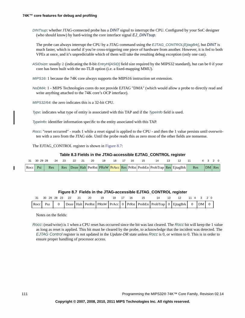
74K™ core features for debug and profiling
111 Programming the MIPS32® 74K™ Core Family, Revision 02.14
Copyright © 2007, 2008, 2010, 2011 MIPS Technologies Inc. All rights reserved.
DINTsup: whether JTAG-connected probe has a DINT signal to interrupt the CPU. Configured by your SoC designer(who should know) by hard-wiring the core interface signal EJ_DINTsup.
The probe can always interrupt the CPU by a JTAG command using the EJTAG_CONTROL[EjtagBrk], but DINT ismuch faster, which is useful if you’re cross-triggering one piece of hardware from another. However, it is fed to bothVPEs at once, and it’s unpredictable which of them will take the resulting debug exception (only one can).
ASIDsize: usually 2 (indicating the 8-bit EntryHi[ASID] field size required by the MIPS32 standard), but can be 0 if yourcore has been built with the no-TLB option (i.e. a fixed-mapping MMU).
MIPS16: 1 because the 74K core always supports the MIPS16 instruction set extension.
NoDMA: 1 - MIPS Technologies cores do not provide EJTAG "DMA" (which would allow a probe to directly read andwrite anything attached to the 74K core’s OCP interface).
MIPS32/64: the zero indicates this is a 32-bit CPU.
Type: indicates what type of entity is associated with this TAP and if the TypeInfo field is used.
TypeInfo: identifier information specific to the entity associated with this TAP.
Rocc: "reset occurred" - reads 1 while a reset signal is applied to the CPU - and then the 1 value persists until overwrit-ten with a zero from the JTAG side. Until the probe reads this as zero most of the other fields are nonsense.
The EJTAG_CONTROL register is shown in Figure 8.7:
Table 8.3 Fields in the JTAG-accessible EJTAG_CONTROL register
Notes on the fields:
Rocc: (read/write) is 1 when a CPU reset has occurred since the bit was last cleared. The Rocc bit will keep the 1 valueas long as reset is applied. This bit must be cleared by the probe, to acknowledge that the incident was detected. TheEJTAG Control register is not updated in the Update-DR state unless Rocc is 0, or written to 0. This is in order toensure proper handling of processor access.
31 30 29 28 24 23 22 21 20 19 18 17 16 15 14 13 12 11 4 3 2 0
Rocc Psi Res Res Doze Halt PerRst PRnW PrAcc Res PrRst ProbEn ProbTrap Res EjtagBrk Res DM Res
Figure 8.7 Fields in the JTAG-accessible EJTAG_CONTROL register31 30 29 28 23 22 21 20 19 18 17 16 15 14 13 12 11 4 3 2 0
Rocc Psz 0 Doze Halt PerRst PRnW PrAcc 0 PrRst ProbEn ProbTrap 0 EjtagBrk 0 DM 0
8.1 EJTAG on-chip debug unit
Programming the MIPS32® 74K™ Core Family, Revision 02.14 112
Copyright © 2007, 2008, 2010, 2011 MIPS Technologies Inc. All rights reserved.
Psz: (read-only) when software reads or writes "dmseg" this tells the probe whether it was a word, byte or whatever-sizetransfer:
Doze/Halt: (read-only) indicates CPU not fully awake. Doze reflects any reduced-power mode, whereas Halt is set onlyif the CPU is asleep after a wait or similar.
PerRst: write to set the EJ_PerRst output signal from the core, which can be used to reset non-core logic (ask yourSoC designer whether it’s connected to anything).
For this and all other fields which change core state, we recommend that the probe should write the field and then pollfor the change to be reflected in this register, which may take a short while. In some cases the bit is just an output one,when the readback will be pointless (but harmless).
PRnW/PrAcc: PrAcc is 1 when the CPU is doing a read/write of the "dmseg" region, and the probe should service it. The"slow" read/write protocol involves the probe flipping this bit back to zero to tell the CPU the transfer is ready.
While PrAcc is active the read-only PRnW bit distinguishes writes (1) from reads (0).
PrRst: controls the EJ_PrRst signal from the core, which may be wired back to reset the CPU and related logic. Writea 1 to reset. If it works, the probe will eventually see the bit fall back to 0 by itself, as the CPU resets. Most probes arewired up with a direct CPU reset signal, which is more reliable.
ProbEn, ProbTrap, EjtagBrk: ProbEn must be set before CPU accesses to "dmseg" will be sent to the probe. It can be
written by the probe directly. ProbTrap relocates the debug exception entry point from 0xBFC0.048026 (when 0) tothe “dmseg” location 0xFF20.0200 - required when the debug exception handler itself is supplied by the probe.
EjtagBrk can be written 1 to "interrupt" the CPU into debug mode.
The three come together into a trick to support systems wanting to boot from EJTAG. The value of all these three bitsis preset by the “EJTAGBOOT” JTAG instruction. When the CPU resets with all of these set to 1, then the CPU willimmediately enter debug mode and start reading instructions from the probe.
DM: (read-only) indicates the CPU is in debug mode, a probe-readable version of Debug[DM].
8.1.10 Fast Debug Channel
The Fast Debug Channel (or FDC) is an interesting creature. It provides a mechanism for data transfers between theprobe and the core, but unlike some of the other mechanisms of that type, it is not constrained to debug mode access.Kernel mode software can access the memory mapped interface and can even grant access rights to user or supervisorprograms. The memory mapped registers provide basic configuration, status, and control information as well as giv-
Byte-within-word Size code Transfer Sizeaddress
EJTAG_ADDRESS[1-0] EJTAG_CONTROL[Psz]
X 0 Byte00 1 Halfword10
00 2 Word00 3 Tri-byte (lowest address 3 bytes)01 Tri-byte (highest address 3 bytes)
26. The ROM-exception-area debug entry point can be relocated by hardware option, see Table 5.1 and its notes.
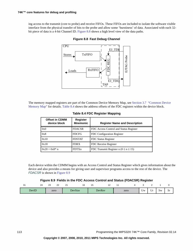
74K™ core features for debug and profiling
113 Programming the MIPS32® 74K™ Core Family, Revision 02.14
Copyright © 2007, 2008, 2010, 2011 MIPS Technologies Inc. All rights reserved.
ing access to the transmit (core to probe) and receive FIFOs. These FIFOs are included to isolate the software visibleinterface from the physical transfer of bits to the probe and allow some ‘burstiness’ of data. Associated with each 32-bit piece of data is a 4-bit Channel ID. Figure 8.8 shows a high level view of the data paths.
Figure 8.8 Fast Debug Channel
The memory mapped registers are part of the Common Device Memory Map, see Section 3.7 “Common DeviceMemory Map” for details. Table 8.4 shows the address offsets of the FDC registers within the device block.
Each device within the CDMM begins with an Access Control and Status Register which gives information about thedevice and also provides a means for giving user and supervisor programs access to the rest of the device. TheFDACSR is shown in Figure 8.9
Figure 8.9 Fields in the FDC Access Control and Status (FDACSR) Register
Table 8.4 FDC Register Mapping
Offset in CDMMdevice block
RegisterMnemonic Register Name and Description
0x0 FDACSR FDC Access Control and Status Register
0x8 FDCFG FDC Configuration Register
0x10 FDSTAT FDC Status Register
0x18 FDRX FDC Receive Register
0x20 + 0x8* n FDTXn FDC Transmit Register n (0 ≤ n ≤ 15)
31 24 23 22 21 16 15 12 11 4 3 2 1 0
DevID zero DevSize DevRev zero Uw Ur Sw Sr
EJ_TDI
EJ_TDO
FDC
RE
G
TxFIFO
RxFIFO
CPU
Stores
Loads
TAP
EJT
AG
Pro
be
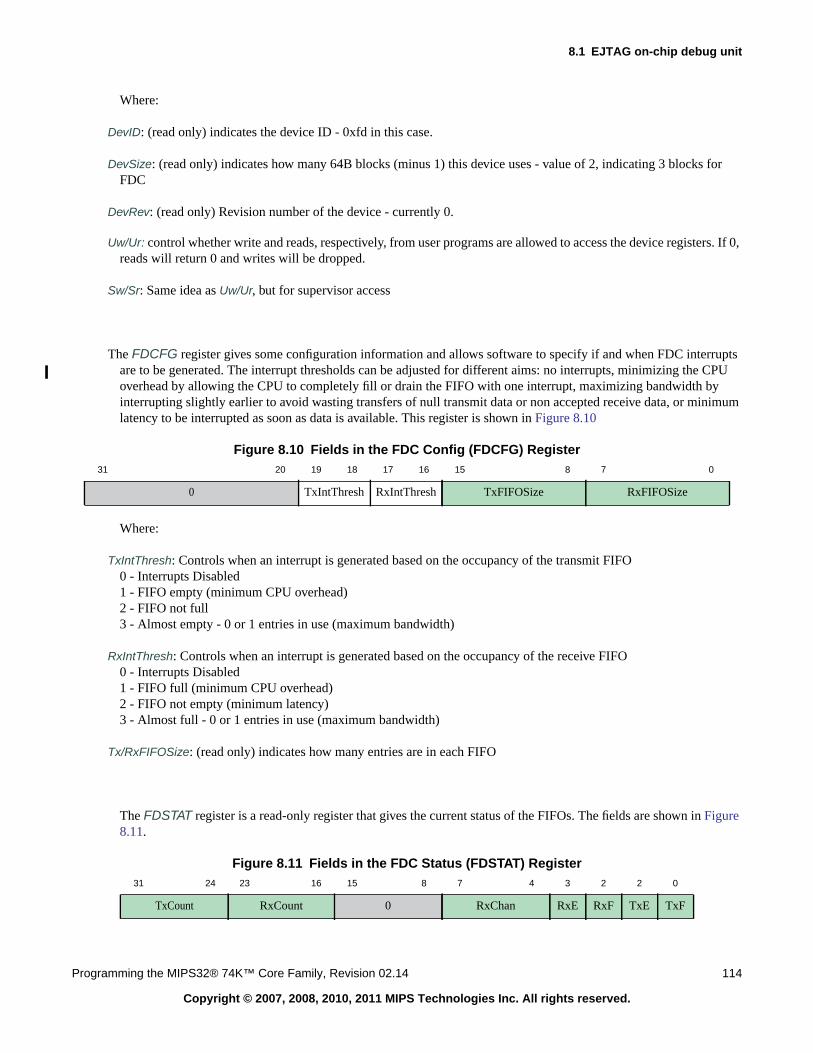
8.1 EJTAG on-chip debug unit
Programming the MIPS32® 74K™ Core Family, Revision 02.14 114
Copyright © 2007, 2008, 2010, 2011 MIPS Technologies Inc. All rights reserved.
Where:
DevID: (read only) indicates the device ID - 0xfd in this case.
DevSize: (read only) indicates how many 64B blocks (minus 1) this device uses - value of 2, indicating 3 blocks forFDC
DevRev: (read only) Revision number of the device - currently 0.
Uw/Ur: control whether write and reads, respectively, from user programs are allowed to access the device registers. If 0,reads will return 0 and writes will be dropped.
Sw/Sr: Same idea as Uw/Ur, but for supervisor access
The FDCFG register gives some configuration information and allows software to specify if and when FDC interruptsare to be generated. The interrupt thresholds can be adjusted for different aims: no interrupts, minimizing the CPUoverhead by allowing the CPU to completely fill or drain the FIFO with one interrupt, maximizing bandwidth byinterrupting slightly earlier to avoid wasting transfers of null transmit data or non accepted receive data, or minimumlatency to be interrupted as soon as data is available. This register is shown in Figure 8.10
Figure 8.10 Fields in the FDC Config (FDCFG) Register
Where:
TxIntThresh: Controls when an interrupt is generated based on the occupancy of the transmit FIFO0 - Interrupts Disabled1 - FIFO empty (minimum CPU overhead)2 - FIFO not full3 - Almost empty - 0 or 1 entries in use (maximum bandwidth)
RxIntThresh: Controls when an interrupt is generated based on the occupancy of the receive FIFO0 - Interrupts Disabled1 - FIFO full (minimum CPU overhead)2 - FIFO not empty (minimum latency)3 - Almost full - 0 or 1 entries in use (maximum bandwidth)
Tx/RxFIFOSize: (read only) indicates how many entries are in each FIFO
The FDSTAT register is a read-only register that gives the current status of the FIFOs. The fields are shown in Figure8.11.
Figure 8.11 Fields in the FDC Status (FDSTAT) Register
31 20 19 18 17 16 15 8 7 0
0 TxIntThresh RxIntThresh TxFIFOSize RxFIFOSize
31 24 23 16 15 8 7 4 3 2 2 0
TxCount RxCount 0 RxChan RxE RxF TxE TxF
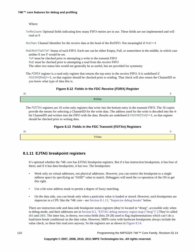
74K™ core features for debug and profiling
115 Programming the MIPS32® 74K™ Core Family, Revision 02.14
Copyright © 2007, 2008, 2010, 2011 MIPS Technologies Inc. All rights reserved.
Where:
Tx/RxCount: Optional fields indicating how many FIFO entries are in use. These fields are not implemented and willread as 0
RxChan: Channel Identifier for the receive data at the head of the RxFIFO. Not meaningful if RxE==1
RxE/RxF/TxE/TxF: Status of each FIFO. Each one can be either Empty, Full, or somewhere in the middle, in which caseneither E nor F would be set.TxF must be checked prior to attempting a write to the transmit FIFORxE must be checked prior to attempting a read from the receive FIFOThe other two status bits would not generally be as useful, but are provided for symmetry
The FDRX register is a read-only register that returns the top entry in the receive FIFO. It is undefined ifFDSTAT[RxE]==1, so that register should be checked prior to reading. That check will also return the ChannelID soyou know what type of data this is.
Figure 8.12 Fields in the FDC Receive (FDRX) Register
The FDTXn registers are 16 write-only registers that write into the bottom entry in the transmit FIFO. The 16 copiesprovide the means for selecting a ChannelID for the write data. The address used for the write is decoded into the 4-bit ChannelID and written into the FIFO with the data. Results are undefined if FDSTAT[TxF]==1, so that registershould be checked prior to writing data.
Figure 8.13 Fields in the FDC Transmit (FDTXn) Registers
8.1.11 EJTAG breakpoint registers
It’s optional whether the 74K core has EJTAG breakpoint registers. But if it has instruction breakpoints, it has four ofthem; and if it has data breakpoints, it has two. The breakpoints:
• Work only on virtual addresses, not physical addresses. However, you can restrict the breakpoint to a singleaddress space by specifying an “ASID” value to match. Debuggers will need the co-operation of the OS to getthis right.
• Use a bit-wise address mask to permit a degree of fuzzy matching.
• On the data side, you can break only when a particular value is loaded or stored. However, such breakpoints areimprecise in a CPU like the 74K core - see Section 8.1.13, "Imprecise debug breaks" below.
There are instruction-side and data-side breakpoint status registers (they’re located in “drseg”, accessible only whenin debug mode, and their addresses are in Section 8.2, "EJTAG debug memory region map (“dseg”)".) They’re calledIBS and DBS. The latter has, in theory, two extra fields (bits 29-28) used to flag implementations which can’t do aload/store break conditional on the data value. However, MIPS cores with hardware breakpoints always include thevalue check, so these bits read zero anyway. So the registers are as shown in Figure 8.14.
31 0
RxData
31 0
TxData
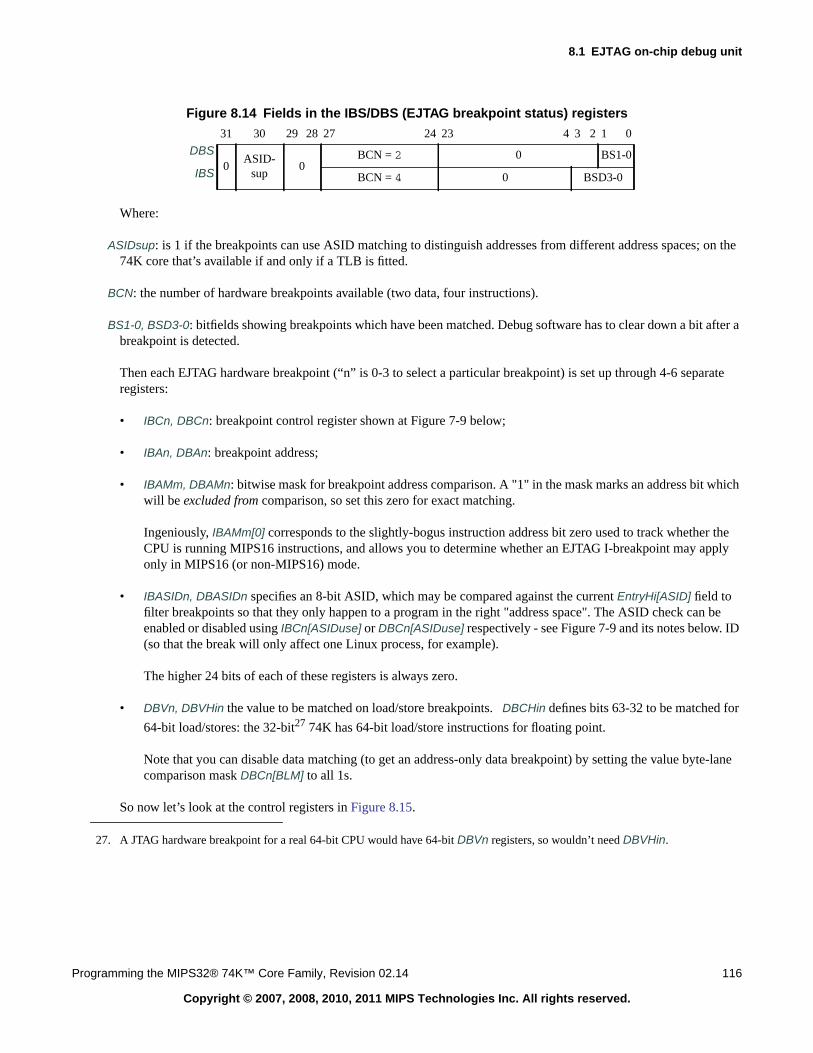
8.1 EJTAG on-chip debug unit
Programming the MIPS32® 74K™ Core Family, Revision 02.14 116
Copyright © 2007, 2008, 2010, 2011 MIPS Technologies Inc. All rights reserved.
Where:
ASIDsup: is 1 if the breakpoints can use ASID matching to distinguish addresses from different address spaces; on the74K core that’s available if and only if a TLB is fitted.
BCN: the number of hardware breakpoints available (two data, four instructions).
BS1-0, BSD3-0: bitfields showing breakpoints which have been matched. Debug software has to clear down a bit after abreakpoint is detected.
Then each EJTAG hardware breakpoint (“n” is 0-3 to select a particular breakpoint) is set up through 4-6 separateregisters:
• IBCn, DBCn: breakpoint control register shown at Figure 7-9 below;
• IBAn, DBAn: breakpoint address;
• IBAMm, DBAMn: bitwise mask for breakpoint address comparison. A "1" in the mask marks an address bit whichwill be excluded from comparison, so set this zero for exact matching.
Ingeniously, IBAMm[0] corresponds to the slightly-bogus instruction address bit zero used to track whether theCPU is running MIPS16 instructions, and allows you to determine whether an EJTAG I-breakpoint may applyonly in MIPS16 (or non-MIPS16) mode.
• IBASIDn, DBASIDn specifies an 8-bit ASID, which may be compared against the current EntryHi[ASID] field tofilter breakpoints so that they only happen to a program in the right "address space". The ASID check can beenabled or disabled using IBCn[ASIDuse] or DBCn[ASIDuse] respectively - see Figure 7-9 and its notes below. ID(so that the break will only affect one Linux process, for example).
The higher 24 bits of each of these registers is always zero.
• DBVn, DBVHin the value to be matched on load/store breakpoints. DBCHin defines bits 63-32 to be matched for
64-bit load/stores: the 32-bit27 74K has 64-bit load/store instructions for floating point.
Note that you can disable data matching (to get an address-only data breakpoint) by setting the value byte-lanecomparison mask DBCn[BLM] to all 1s.
So now let’s look at the control registers in Figure 8.15.
Figure 8.14 Fields in the IBS/DBS (EJTAG breakpoint status) registers31 30 29 28 27 24 23 4 3 2 1 0
DBS0
ASID-sup
0BCN = 2 0 BS1-0
IBS BCN = 4 0 BSD3-0
27. A JTAG hardware breakpoint for a real 64-bit CPU would have 64-bit DBVn registers, so wouldn’t need DBVHin.
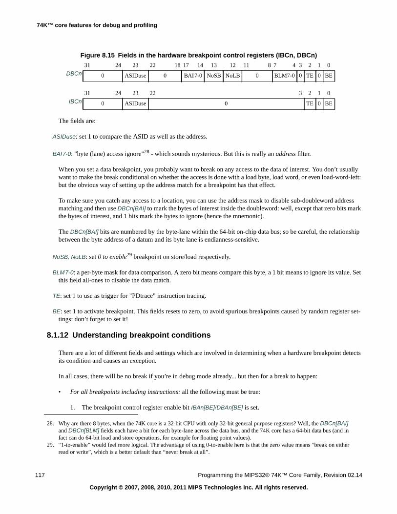
74K™ core features for debug and profiling
117 Programming the MIPS32® 74K™ Core Family, Revision 02.14
Copyright © 2007, 2008, 2010, 2011 MIPS Technologies Inc. All rights reserved.
The fields are:
ASIDuse: set 1 to compare the ASID as well as the address.
BAI7-0: "byte (lane) access ignore"28 - which sounds mysterious. But this is really an address filter.
When you set a data breakpoint, you probably want to break on any access to the data of interest. You don’t usuallywant to make the break conditional on whether the access is done with a load byte, load word, or even load-word-left:but the obvious way of setting up the address match for a breakpoint has that effect.
To make sure you catch any access to a location, you can use the address mask to disable sub-doubleword addressmatching and then use DBCn[BAI] to mark the bytes of interest inside the doubleword: well, except that zero bits markthe bytes of interest, and 1 bits mark the bytes to ignore (hence the mnemonic).
The DBCn[BAI] bits are numbered by the byte-lane within the 64-bit on-chip data bus; so be careful, the relationshipbetween the byte address of a datum and its byte lane is endianness-sensitive.
NoSB, NoLB: set 0 to enable29 breakpoint on store/load respectively.
BLM7-0: a per-byte mask for data comparison. A zero bit means compare this byte, a 1 bit means to ignore its value. Setthis field all-ones to disable the data match.
TE: set 1 to use as trigger for "PDtrace" instruction tracing.
BE: set 1 to activate breakpoint. This fields resets to zero, to avoid spurious breakpoints caused by random register set-tings: don’t forget to set it!
8.1.12 Understanding breakpoint conditions
There are a lot of different fields and settings which are involved in determining when a hardware breakpoint detectsits condition and causes an exception.
In all cases, there will be no break if you’re in debug mode already... but then for a break to happen:
• For all breakpoints including instructions: all the following must be true:
1. The breakpoint control register enable bit IBAn[BE]/DBAn[BE] is set.
Figure 8.15 Fields in the hardware breakpoint control registers (IBCn, DBCn)31 24 23 22 18 17 14 13 12 11 8 7 4 3 2 1 0
DBCn 0 ASIDuse 0 BAI7-0 NoSB NoLB 0 BLM7-0 0 TE 0 BE
31 24 23 22 3 2 1 0
IBCn 0 ASIDuse 0 TE 0 BE
28. Why are there 8 bytes, when the 74K core is a 32-bit CPU with only 32-bit general purpose registers? Well, the DBCn[BAI]and DBCn[BLM] fields each have a bit for each byte-lane across the data bus, and the 74K core has a 64-bit data bus (and infact can do 64-bit load and store operations, for example for floating point values).
29. “1-to-enable” would feel more logical. The advantage of using 0-to-enable here is that the zero value means “break on eitherread or write”, which is a better default than “never break at all”.
8.1 EJTAG on-chip debug unit
Programming the MIPS32® 74K™ Core Family, Revision 02.14 118
Copyright © 2007, 2008, 2010, 2011 MIPS Technologies Inc. All rights reserved.
2. the address generated by the program for instruction fetch, load or store matches those bits of the break-point’s address register IBAn/DBAn for which the corresponding address-mask register bits in IBAn/DBAn arezero.
3. either IBCn[ASIDuse]/DBCn[ASIDuse] is zero (so we don’t care what address space we’re matching against),OR the address-space ID of the running program, i.e. EntryHi[ASID], is equal to the value in IBASIDn/DBASIDn.
That’s all for instruction breakpoints, but for data-side breakpoints also:
• Data compare break conditions (not value related): both the following must be true:
4. It’s a load and DBCn[NoLB] is zero, or it’s a store and DBCn[NoSB] is zero.
5. The load or the store touches at least one byte-within-doubleword for which the corresponding DBCn[BAI]bit is zero.
If you didn’t want to compare the load/store value then DBCn[BLM] will be all-ones, and you’re done. But if youalso want to consider the value:
• Data value compare break conditions:
6. the data loaded or stored, as it would appear on the system bus, matches the 64-bit contents of DBVHin withDBVn in each of those 8-bit groups for which the corresponding bit in DBCn[BLM] is zero.
That’s it.
8.1.13 Imprecise debug breaks
Instruction breakpoints, and data breakpoints filtering only on address conditions are precise; that means that:
1. DEPC will point at the fetched or load/store instruction itself (except if it’s in a branch delay slot, will point at thebranch instruction);
2. The instruction will not have caused any side effects; in particular, the load/store will not reach the cache ormemory.
Most exceptions in MIPS architecture CPUs are precise. But because of the way the 74K core optimizes loads andstores by permitting the CPU to run on at least until it needs to use the data from a load, data breakpoints which filteron the data value are imprecise. The debug exception will happen to whatever instruction (typically later in theinstruction stream) is running when the hardware detects the match, and not necessarily to the same TC. The debug-ging software must cope.
8.1.14 PC Sampling with EJTAG
A valuable trick available with recent revisions of the EJTAG specification and probes, “PC sampling” provides anon-intrusive way to collect statistical information about the activity of a running system. You can tell whether PCsampling is enabled by looking at DCR[PCS], as shown in Figure 7-5 above.
The hardware snapshots the “current PC” periodically, and stores that value where it can be retrieved by a debugprobe. It’s then up to software to construct a histogram of samples over a period of time, which (statistically) allows aprogrammer to see where the CPU has spent most cycles. Not only is this useful, but it’s also familiar: systems have
74K™ core features for debug and profiling
119 Programming the MIPS32® 74K™ Core Family, Revision 02.14
Copyright © 2007, 2008, 2010, 2011 MIPS Technologies Inc. All rights reserved.
used intrusive interrupt-based PC-sampling for many years, so there are tools which can readily interpret this sort ofdata.
When PC sampling is configured in your core, it runs continuously. Some sleight of hand is used if the CPU is hang-ing on a wait instruction. Rather than wasting even a small amount of power running the counter and resampling thePC of the wait instruction, the hardware simply keeps the “new” bit set while it is in this state telling the profilingsoftware that yes, we are still at that instruction. You can choose to sample as often as once per 32 cycles or as rarely
as once per 4096 cycles30; at every sampling point the address of the instruction completing in that cycle (or if nonecompletes, the address of the next instruction to complete) is deposited in a JTAG-accessible register. Sampling rate iscontrolled by the DCR[PCR] field of the debug control register shown in Figure 7-5.
In addition to the 32 bits of the instruction address, several other fields are stored by the hardware to help identify theinstruction. The aforementioned “new” bit indicates a new sample, which a probe can use to avoid double-countingthe same sample. On multi-threaded CPUs where there might be several copies of the code running, a TCID field isalso appended. The then-current ASID may also be included so that you can interpret the virtual PC. The ASID isincluded unless the DCR[PCnoASID] bit is set. This bit may be hardwired in a given implementation or the bit mightbe writable, so go ahead and try to change it if you feel like it (but be sure to read it back and see if the write ‘stuck’so that you know how many bits to scan and how to interpret them).
EJTAG revision 5.0 adds a new optional mechanism for triggering PC sampling when an instruction fetch misses inthe I-cache. When the PCIM and PCSe fields of the Debug Control Register (DCR[26] and DCR[5]) are set to 1,instructions that miss in the I-cache and all the uncached fetches are captured. The capturing of the I-cache missesdoes not depend on the PC Sampling Rate (DCR[8:6]). Whenever there is a miss, that PC will be captured. The cap-tured PC will be sent to EJTAG to shift out through PCSAMPLE. Over time, this collection mode results in an overallpicture of the instruction cache behavior and can be used to increase performance by re-arranging code to minimizecache thrashing.
8.1.15 JTAG-accessible and memory-mapped PDtrace TCB Registers
The DCR and the hardware breakpoint registers are EJTAG registers that are both JTAG-accessible and memory-mapped. In addition to the DCR and the hardware breakpoint registers, the EJTAG PDtrace Registers listed in Table8.5 are also memory-mapped to drseg. These registers allow software to access the on-chip trace memory. A loadfrom the EJAG register TCBTW will return the data at the address location pointed to by the read pointer TCBRDP.See the Software User’s Manual for more details and rules to access the on-chip trace memory.
30. Since it runs continuously, it’s a good thing that from reset the sampling period defaults to its maximum.
Table 8.5 Mapping TCB Registers in drseg
Offset in drseg Register Name Description
0x3000 TCBControlA The TCBControlA register.
0x3008 TCBControlB The TCBControlB register.
0x3010 TCBControlC The TCBControlC register.
0x3018 TCBControlD The TCBControlD register.
0x3020 TCBControlE The TCBControlE register.
0x3028 TCBConfig The TCBConfig register.
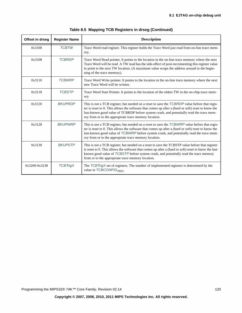
8.1 EJTAG on-chip debug unit
Programming the MIPS32® 74K™ Core Family, Revision 02.14 120
Copyright © 2007, 2008, 2010, 2011 MIPS Technologies Inc. All rights reserved.
0x3100 TCBTW Trace Word read register. This register holds the Trace Word just read from on-line trace mem-ory.
0x3108 TCBRDP Trace Word Read pointer. It points to the location in the on-line trace memory where the nextTrace Word will be read. A TW read has the side-effect of post-incrementing this register valueto point to the next TW location. (A maximum value wraps the address around to the begin-ning of the trace memory).
0x3110 TCBWRP Trace Word Write pointer. It points to the location in the on-line trace memory where the nextnew Trace Word will be written.
0x3118 TCBSTP Trace Word Start Pointer. It points to the location of the oldest TW in the on-chip trace mem-ory.
0x3120 BKUPRDP This is not a TCB register, but needed on a reset to save the TCBRDP value before that regis-ter is reset to 0. This allows the software that comes up after a (hard or soft) reset to know thelast-known good value of TCBRDP before system crash, and potentially read the trace mem-ory from or to the appropriate trace memory location.
0x3128 BKUPWRP This is not a TCB register, but needed on a reset to save the TCBWRP value before that regis-ter is reset to 0. This allows the software that comes up after a (hard or soft) reset to know thelast-known good value of TCBWRP before system crash, and potentially read the trace mem-ory from or to the appropriate trace memory location.
0x3130 BKUPSTP This is not a TCB register, but needed on a reset to save the TCBSTP value before that registeris reset to 0. This allows the software that comes up after a (hard or soft) reset to know the last-known good value of TCBSTP before system crash, and potentially read the trace memoryfrom or to the appropriate trace memory location.
0x3200-0x3238 TCBTrigX The TCBTrigX set of registers. The number of implemented registers is determined by thevalue in TCBCONFIGTRIG.
Table 8.5 Mapping TCB Registers in drseg (Continued)
Offset in drseg Register Name Description
121 Programming the MIPS32® 74K™ Core Family, Revision 02.14
Copyright © 2007, 2008, 2010, 2011 MIPS Technologies Inc. All rights reserved.
8.2 PDtrace™ instruction trace facility
An instruction trace is a set of data generated when a program runs which allows you to recreate the sequence ofinstructions executed, possibly with additional information included about data values. Instruction traces rapidlybecome enormous, and are typically generated in some kind of abbreviated form, which may be reconstructed bysoftware which is in possession of a copy of the binary code of your system.
74K family cores can be configured with PDtrace logic, which provides a non-intrusive way of finding out whatinstructions your CPU ran. If your system includes PDtrace logic, Config3[TL] will read 1.
With a very high-speed CPU like the 74K core this is challenging, because you need to send data so fast. The PDtracesystem deals with this by:
• Compressing the trace: a software tool in possession of the binary of your program can predict where executionwill go next, following sequential instructions and fixed branches. To trace your program it needs only to knowwhether conditional branches were taken, and the destination of computed branches like jump-register.
• Switching the trace on and off: the 74K core can be configured with up to 8 “trace triggers”, allowing you to startand stop tracing based on EJTAG breakpoint matches: see Section 8.1.11, "EJTAG breakpoint registers" aboveand Table 8.21 below.
• High-speed connection to a debug/trace probe: optional. But if fitted, it uses advanced signalling techniques toget trace data from the CPU core, out of dedicated package pins to a probe. Good probes have generous amountsof high-speed memory to store long traces.
TraceControl2[ValidModes,TBI,TBU] (described below at Figure 7-10 and following) tell you whether you havesuch a connection available on your core. You’ll have to ask the hardware engineers whether they brought out theconnector, of course.
• Very high-speed on-chip trace memory: if fitted, you may find between 256bytes and 8Mbytes of trace memoryin your system (larger than a few Kbytes is unlikely). Again, see TraceControl2[ValidModes,TBI,TBU] to find outwhat facilities you have.
• Option to slow the CPU to match the tracing speed: when you really, really need a full trace, and are prepared toslow down your program if necessary to wait while the trace information is sent to the probe. This is controlledby TraceControl[IO], see below.
• Software access to on-chip trace memory : A new mechanism is provided to allow software to read the on-chiptrace memory. This is achieved by mapping all the TCB registers to drseg.
In practice the PDtrace logic depends on the existence of an EJTAG unit (described in the previous section) and anenhanced EJTAG probe. To benefit from on-probe trace memory, the probe will need to attach to PDtrace-specificsignals.
This manual describes only the lowest-level building blocks as visible to software. For real hardware informationrefer to [PDTRACETCB]; for guidance about how to use the PDtrace facilities for software development see[PDTRACEUSAGE]. To use PDtrace facilities, you’ll have to read the software manuals which come with a probe.
8.2.1 74K core-specific fields in PDtrace™ JTAG-accessible registers
The PDtrace system is controlled by the JTAG-accessible registers TCBCONTROLA, TCBCONTROLB, TCBCON-TROLC, TCBCONTROLD, and TCBCONTROLE. Normally they are not visible to software running on the CPU,
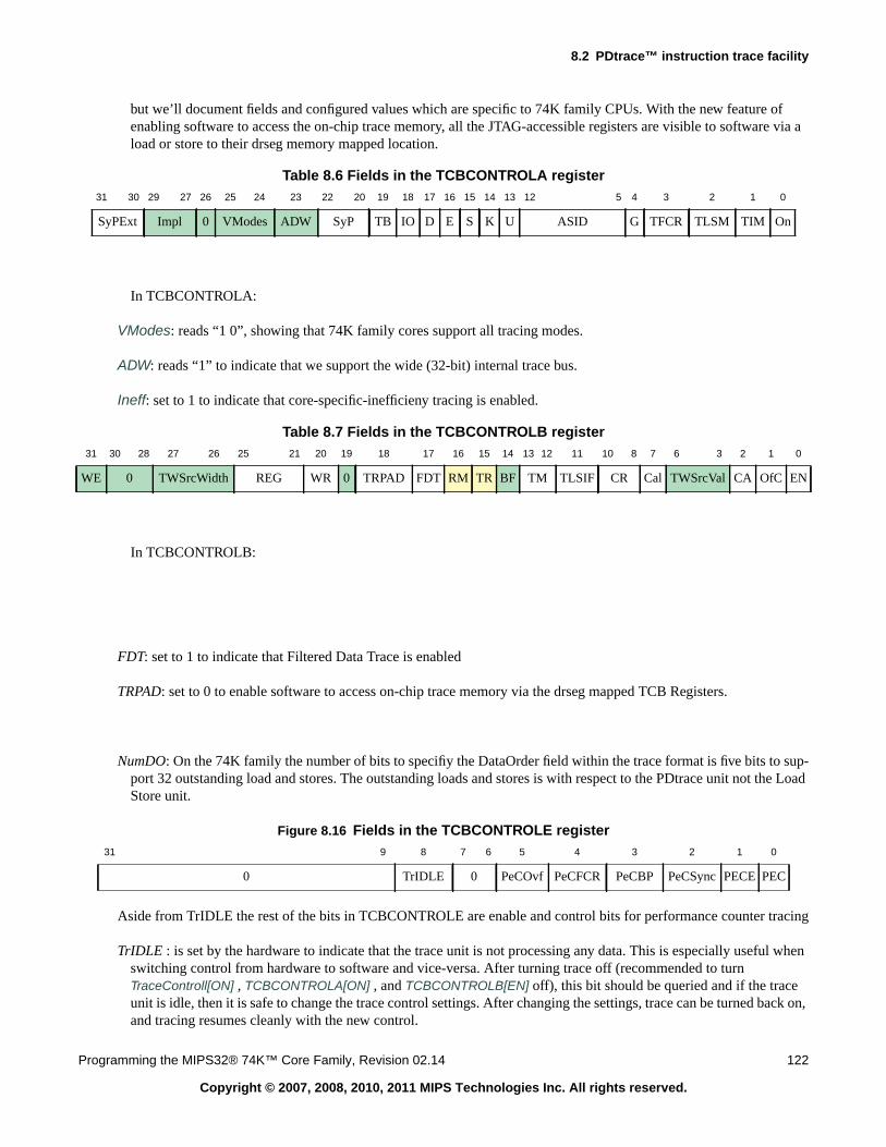
8.2 PDtrace™ instruction trace facility
Programming the MIPS32® 74K™ Core Family, Revision 02.14 122
Copyright © 2007, 2008, 2010, 2011 MIPS Technologies Inc. All rights reserved.
but we’ll document fields and configured values which are specific to 74K family CPUs. With the new feature ofenabling software to access the on-chip trace memory, all the JTAG-accessible registers are visible to software via aload or store to their drseg memory mapped location.
Table 8.6 Fields in the TCBCONTROLA register
In TCBCONTROLA:
VModes: reads “1 0”, showing that 74K family cores support all tracing modes.
ADW: reads “1” to indicate that we support the wide (32-bit) internal trace bus.
Ineff: set to 1 to indicate that core-specific-inefficieny tracing is enabled.
Table 8.7 Fields in the TCBCONTROLB register
In TCBCONTROLB:
FDT: set to 1 to indicate that Filtered Data Trace is enabled
TRPAD: set to 0 to enable software to access on-chip trace memory via the drseg mapped TCB Registers.
NumDO: On the 74K family the number of bits to specifiy the DataOrder field within the trace format is five bits to sup-port 32 outstanding load and stores. The outstanding loads and stores is with respect to the PDtrace unit not the LoadStore unit.
Figure 8.16 Fields in the TCBCONTROLE register
Aside from TrIDLE the rest of the bits in TCBCONTROLE are enable and control bits for performance counter tracing
TrIDLE : is set by the hardware to indicate that the trace unit is not processing any data. This is especially useful whenswitching control from hardware to software and vice-versa. After turning trace off (recommended to turnTraceControll[ON] , TCBCONTROLA[ON] , and TCBCONTROLB[EN] off), this bit should be queried and if the traceunit is idle, then it is safe to change the trace control settings. After changing the settings, trace can be turned back on,and tracing resumes cleanly with the new control.
31 30 29 27 26 25 24 23 22 20 19 18 17 16 15 14 13 12 5 4 3 2 1 0
SyPExt Impl 0 VModes ADW SyP TB IO D E S K U ASID G TFCR TLSM TIM On
31 30 28 27 26 25 21 20 19 18 17 16 15 14 13 12 11 10 8 7 6 3 2 1 0
WE 0 TWSrcWidth REG WR 0 TRPAD FDT RM TR BF TM TLSIF CR Cal TWSrcVal CA OfC EN
31 9 8 7 6 5 4 3 2 1 0
0 TrIDLE 0 PeCOvf PeCFCR PeCBP PeCSync PECE PEC
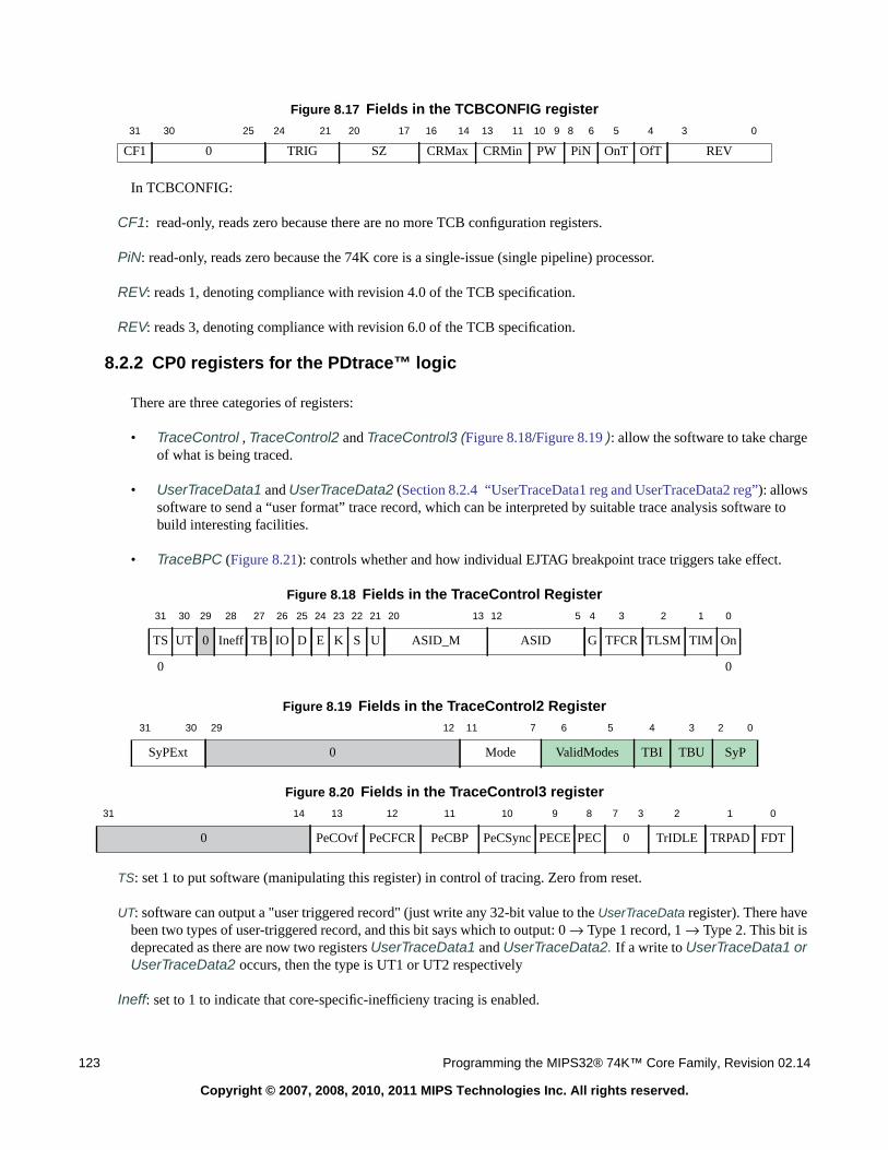
123 Programming the MIPS32® 74K™ Core Family, Revision 02.14
Copyright © 2007, 2008, 2010, 2011 MIPS Technologies Inc. All rights reserved.
Figure 8.17 Fields in the TCBCONFIG register
In TCBCONFIG:
CF1: read-only, reads zero because there are no more TCB configuration registers.
PiN: read-only, reads zero because the 74K core is a single-issue (single pipeline) processor.
REV: reads 1, denoting compliance with revision 4.0 of the TCB specification.
REV: reads 3, denoting compliance with revision 6.0 of the TCB specification.
8.2.2 CP0 registers for the PDtrace™ logic
There are three categories of registers:
• TraceControl , TraceControl2 and TraceControl3 (Figure 8.18/Figure 8.19 ): allow the software to take chargeof what is being traced.
• UserTraceData1 and UserTraceData2 (Section 8.2.4 “UserTraceData1 reg and UserTraceData2 reg”): allowssoftware to send a “user format” trace record, which can be interpreted by suitable trace analysis software tobuild interesting facilities.
• TraceBPC (Figure 8.21): controls whether and how individual EJTAG breakpoint trace triggers take effect.
Figure 8.18 Fields in the TraceControl Register
Figure 8.19 Fields in the TraceControl2 Register
Figure 8.20 Fields in the TraceControl3 register
TS: set 1 to put software (manipulating this register) in control of tracing. Zero from reset.
UT: software can output a "user triggered record" (just write any 32-bit value to the UserTraceData register). There havebeen two types of user-triggered record, and this bit says which to output: 0 → Type 1 record, 1 → Type 2. This bit isdeprecated as there are now two registers UserTraceData1 and UserTraceData2. If a write to UserTraceData1 orUserTraceData2 occurs, then the type is UT1 or UT2 respectively
Ineff: set to 1 to indicate that core-specific-inefficieny tracing is enabled.
31 30 25 24 21 20 17 16 14 13 11 10 9 8 6 5 4 3 0
CF1 0 TRIG SZ CRMax CRMin PW PiN OnT OfT REV
31 30 29 28 27 26 25 24 23 22 21 20 13 12 5 4 3 2 1 0
TS UT 0 Ineff TB IO D E K S U ASID_M ASID G TFCR TLSM TIM On
0 0
31 30 29 12 11 7 6 5 4 3 2 0
SyPExt 0 Mode ValidModes TBI TBU SyP
31 14 13 12 11 10 9 8 7 3 2 1 0
0 PeCOvf PeCFCR PeCBP PeCSync PECE PEC 0 TrIDLE TRPAD FDT
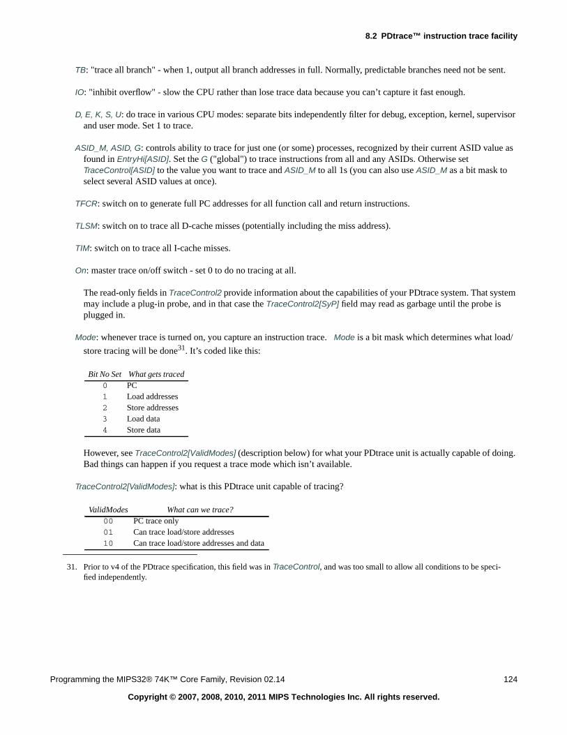
8.2 PDtrace™ instruction trace facility
Programming the MIPS32® 74K™ Core Family, Revision 02.14 124
Copyright © 2007, 2008, 2010, 2011 MIPS Technologies Inc. All rights reserved.
TB: "trace all branch" - when 1, output all branch addresses in full. Normally, predictable branches need not be sent.
IO: "inhibit overflow" - slow the CPU rather than lose trace data because you can’t capture it fast enough.
D, E, K, S, U: do trace in various CPU modes: separate bits independently filter for debug, exception, kernel, supervisorand user mode. Set 1 to trace.
ASID_M, ASID, G: controls ability to trace for just one (or some) processes, recognized by their current ASID value asfound in EntryHi[ASID]. Set the G ("global") to trace instructions from all and any ASIDs. Otherwise setTraceControl[ASID] to the value you want to trace and ASID_M to all 1s (you can also use ASID_M as a bit mask toselect several ASID values at once).
TFCR: switch on to generate full PC addresses for all function call and return instructions.
TLSM: switch on to trace all D-cache misses (potentially including the miss address).
TIM: switch on to trace all I-cache misses.
On: master trace on/off switch - set 0 to do no tracing at all.
The read-only fields in TraceControl2 provide information about the capabilities of your PDtrace system. That systemmay include a plug-in probe, and in that case the TraceControl2[SyP] field may read as garbage until the probe isplugged in.
Mode: whenever trace is turned on, you capture an instruction trace. Mode is a bit mask which determines what load/
store tracing will be done31. It’s coded like this:
However, see TraceControl2[ValidModes] (description below) for what your PDtrace unit is actually capable of doing.Bad things can happen if you request a trace mode which isn’t available.
TraceControl2[ValidModes]: what is this PDtrace unit capable of tracing?
Bit No Set What gets traced0 PC1 Load addresses2 Store addresses3 Load data4 Store data
31. Prior to v4 of the PDtrace specification, this field was in TraceControl, and was too small to allow all conditions to be speci-fied independently.
ValidModes What can we trace?00 PC trace only01 Can trace load/store addresses10 Can trace load/store addresses and data
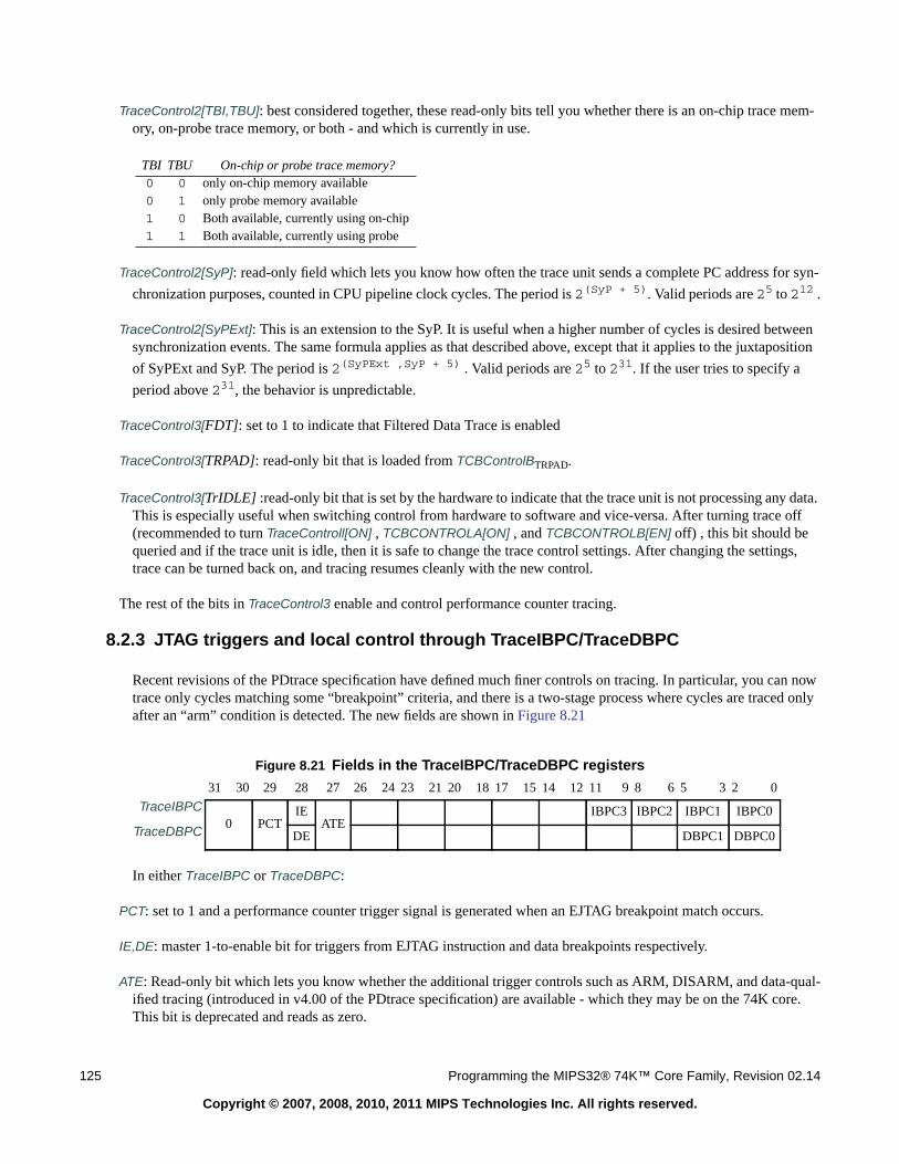
125 Programming the MIPS32® 74K™ Core Family, Revision 02.14
Copyright © 2007, 2008, 2010, 2011 MIPS Technologies Inc. All rights reserved.
TraceControl2[TBI,TBU]: best considered together, these read-only bits tell you whether there is an on-chip trace mem-ory, on-probe trace memory, or both - and which is currently in use.
TraceControl2[SyP]: read-only field which lets you know how often the trace unit sends a complete PC address for syn-
chronization purposes, counted in CPU pipeline clock cycles. The period is 2(SyP + 5). Valid periods are 25 to 212 .
TraceControl2[SyPExt]: This is an extension to the SyP. It is useful when a higher number of cycles is desired betweensynchronization events. The same formula applies as that described above, except that it applies to the juxtaposition
of SyPExt and SyP. The period is 2(SyPExt ,SyP + 5) . Valid periods are 25 to 231. If the user tries to specify a
period above 231, the behavior is unpredictable.
TraceControl3[FDT]: set to 1 to indicate that Filtered Data Trace is enabled
TraceControl3[TRPAD]: read-only bit that is loaded from TCBControlBTRPAD.
TraceControl3[TrIDLE] :read-only bit that is set by the hardware to indicate that the trace unit is not processing any data.This is especially useful when switching control from hardware to software and vice-versa. After turning trace off(recommended to turn TraceControll[ON] , TCBCONTROLA[ON] , and TCBCONTROLB[EN] off) , this bit should bequeried and if the trace unit is idle, then it is safe to change the trace control settings. After changing the settings,trace can be turned back on, and tracing resumes cleanly with the new control.
The rest of the bits in TraceControl3 enable and control performance counter tracing.
8.2.3 JTAG triggers and local control through TraceIBPC/TraceDBPC
Recent revisions of the PDtrace specification have defined much finer controls on tracing. In particular, you can nowtrace only cycles matching some “breakpoint” criteria, and there is a two-stage process where cycles are traced onlyafter an “arm” condition is detected. The new fields are shown in Figure 8.21
In either TraceIBPC or TraceDBPC:
PCT: set to 1 and a performance counter trigger signal is generated when an EJTAG breakpoint match occurs.
IE,DE: master 1-to-enable bit for triggers from EJTAG instruction and data breakpoints respectively.
ATE: Read-only bit which lets you know whether the additional trigger controls such as ARM, DISARM, and data-qual-ified tracing (introduced in v4.00 of the PDtrace specification) are available - which they may be on the 74K core.This bit is deprecated and reads as zero.
TBI TBU On-chip or probe trace memory?0 0 only on-chip memory available0 1 only probe memory available1 0 Both available, currently using on-chip1 1 Both available, currently using probe
Figure 8.21 Fields in the TraceIBPC/TraceDBPC registers31 30 29 28 27 26 24 23 21 20 18 17 15 14 12 11 9 8 6 5 3 2 0
TraceIBPC0 PCT
IEATE
IBPC3 IBPC2 IBPC1 IBPC0
TraceDBPC DE DBPC1 DBPC0
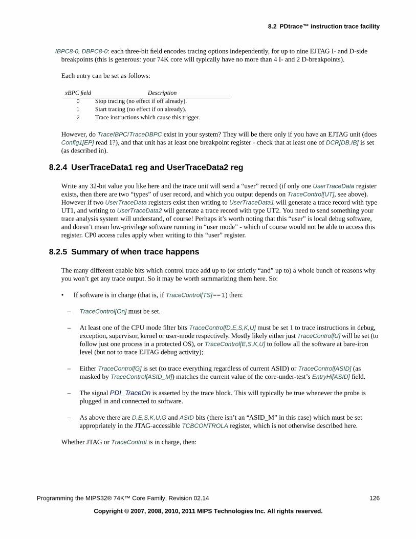
8.2 PDtrace™ instruction trace facility
Programming the MIPS32® 74K™ Core Family, Revision 02.14 126
Copyright © 2007, 2008, 2010, 2011 MIPS Technologies Inc. All rights reserved.
IBPC8-0, DBPC8-0: each three-bit field encodes tracing options independently, for up to nine EJTAG I- and D-sidebreakpoints (this is generous: your 74K core will typically have no more than 4 I- and 2 D-breakpoints).
Each entry can be set as follows:
However, do TraceIBPC/TraceDBPC exist in your system? They will be there only if you have an EJTAG unit (doesConfig1[EP] read 1?), and that unit has at least one breakpoint register - check that at least one of DCR[DB,IB] is set(as described in).
8.2.4 UserTraceData1 reg and UserTraceData2 reg
Write any 32-bit value you like here and the trace unit will send a “user” record (if only one UserTraceData registerexists, then there are two “types” of user record, and which you output depends on TraceControl[UT], see above).However if two UserTraceData registers exist then writing to UserTraceData1 will generate a trace record with typeUT1, and writing to UserTraceData2 will generate a trace record with type UT2. You need to send something yourtrace analysis system will understand, of course! Perhaps it’s worth noting that this “user” is local debug software,and doesn’t mean low-privilege software running in “user mode” - which of course would not be able to access thisregister. CP0 access rules apply when writing to this “user” register.
8.2.5 Summary of when trace happens
The many different enable bits which control trace add up to (or strictly “and” up to) a whole bunch of reasons whyyou won’t get any trace output. So it may be worth summarizing them here. So:
• If software is in charge (that is, if TraceControl[TS]==1) then:
– TraceControl[On] must be set.
– At least one of the CPU mode filter bits TraceControl[D,E,S,K,U] must be set 1 to trace instructions in debug,exception, supervisor, kernel or user-mode respectively. Mostly likely either just TraceControl[U] will be set (tofollow just one process in a protected OS), or TraceControl[E,S,K,U] to follow all the software at bare-ironlevel (but not to trace EJTAG debug activity);
– Either TraceControl[G] is set (to trace everything regardless of current ASID) or TraceControl[ASID] (asmasked by TraceControl[ASID_M]) matches the current value of the core-under-test’s EntryHi[ASID] field.
– The signal PDI_TraceOn is asserted by the trace block. This will typically be true whenever the probe isplugged in and connected to software.
– As above there are D,E,S,K,U,G and ASID bits (there isn’t an “ASID_M” in this case) which must be setappropriately in the JTAG-accessible TCBCONTROLA register, which is not otherwise described here.
Whether JTAG or TraceControl is in charge, then:
xBPC field Description0 Stop tracing (no effect if off already).1 Start tracing (no effect if on already).2 Trace instructions which cause this trigger.
127 Programming the MIPS32® 74K™ Core Family, Revision 02.14
Copyright © 2007, 2008, 2010, 2011 MIPS Technologies Inc. All rights reserved.
• There must have been a cycle recently when there was an “on trigger”, that is:
– The CPU tripped an EJTAG breakpoint with the IBCn[TE]/DBCn[TE] bit set to request a trace trigger (for I-sideand D-side respectively);
– TraceIBPC[IE]/TraceDBPC[DE] (respectively) was set to enable triggers from EJTAG breakpoints;
– the appropriate TraceBPC[IBPCx]/TraceBPC[DBPCx] field has some kind of “on” trigger - and if this trigger isconditional on “arm” there must have been an arm event since system reset or any disarm event; or the triggerunconditionally turns trace on.
• And since the on-trigger time, there must not have been a cycle which acted as an “off trigger”, that is:
– The CPU tripped an EJTAG breakpoint with the IBCn[TE]/DBCn[TE] bit set, and TraceBPC[IE]/TraceBPC[DE](respectively) were still set;
– where the appropriate TraceIBPC[IBPCn]/TraceDBPC[DBPCn] fields is set to disable triggering (subject toarming).
If there is more than one breakpoint match in the same cycle, an “on” trigger wins out over any number of “off”.
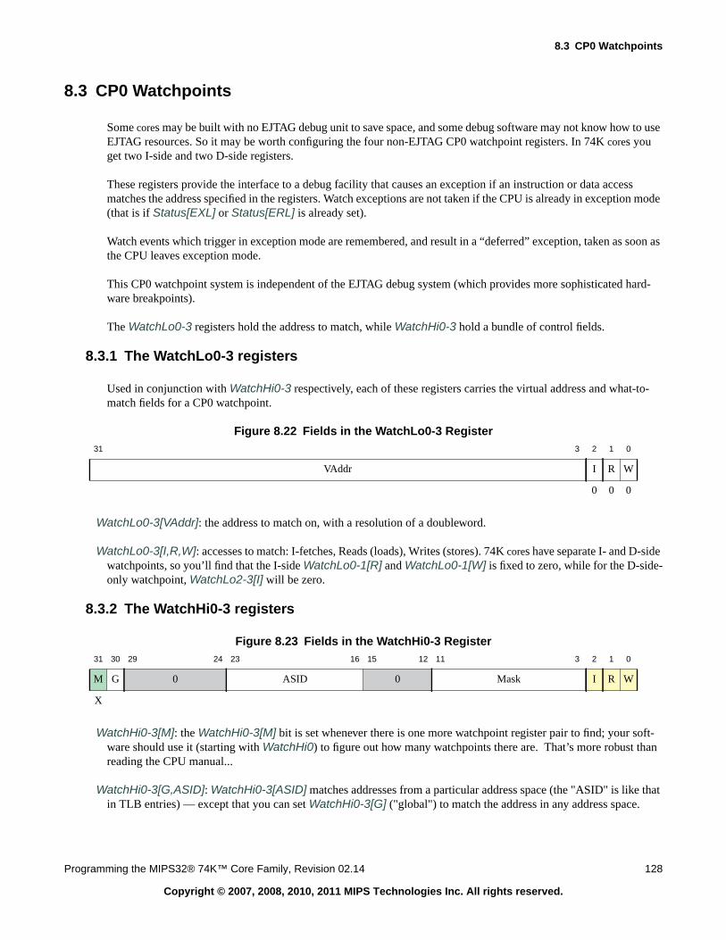
8.3 CP0 Watchpoints
Programming the MIPS32® 74K™ Core Family, Revision 02.14 128
Copyright © 2007, 2008, 2010, 2011 MIPS Technologies Inc. All rights reserved.
8.3 CP0 Watchpoints
Some cores may be built with no EJTAG debug unit to save space, and some debug software may not know how to useEJTAG resources. So it may be worth configuring the four non-EJTAG CP0 watchpoint registers. In 74K cores youget two I-side and two D-side registers.
These registers provide the interface to a debug facility that causes an exception if an instruction or data accessmatches the address specified in the registers. Watch exceptions are not taken if the CPU is already in exception mode(that is if Status[EXL] or Status[ERL] is already set).
Watch events which trigger in exception mode are remembered, and result in a “deferred” exception, taken as soon asthe CPU leaves exception mode.
This CP0 watchpoint system is independent of the EJTAG debug system (which provides more sophisticated hard-ware breakpoints).
The WatchLo0-3 registers hold the address to match, while WatchHi0-3 hold a bundle of control fields.
8.3.1 The WatchLo0-3 registers
Used in conjunction with WatchHi0-3 respectively, each of these registers carries the virtual address and what-to-match fields for a CP0 watchpoint.
Figure 8.22 Fields in the WatchLo0-3 Register
WatchLo0-3[VAddr]: the address to match on, with a resolution of a doubleword.
WatchLo0-3[I,R,W]: accesses to match: I-fetches, Reads (loads), Writes (stores). 74K cores have separate I- and D-sidewatchpoints, so you’ll find that the I-side WatchLo0-1[R] and WatchLo0-1[W] is fixed to zero, while for the D-side-only watchpoint, WatchLo2-3[I] will be zero.
8.3.2 The WatchHi0-3 registers
Figure 8.23 Fields in the WatchHi0-3 Register
WatchHi0-3[M]: the WatchHi0-3[M] bit is set whenever there is one more watchpoint register pair to find; your soft-ware should use it (starting with WatchHi0) to figure out how many watchpoints there are. That’s more robust thanreading the CPU manual...
WatchHi0-3[G,ASID]: WatchHi0-3[ASID] matches addresses from a particular address space (the "ASID" is like thatin TLB entries) — except that you can set WatchHi0-3[G] ("global") to match the address in any address space.
31 3 2 1 0
VAddr I R W
0 0 0
31 30 29 24 23 16 15 12 11 3 2 1 0
M G 0 ASID 0 Mask I R W
X
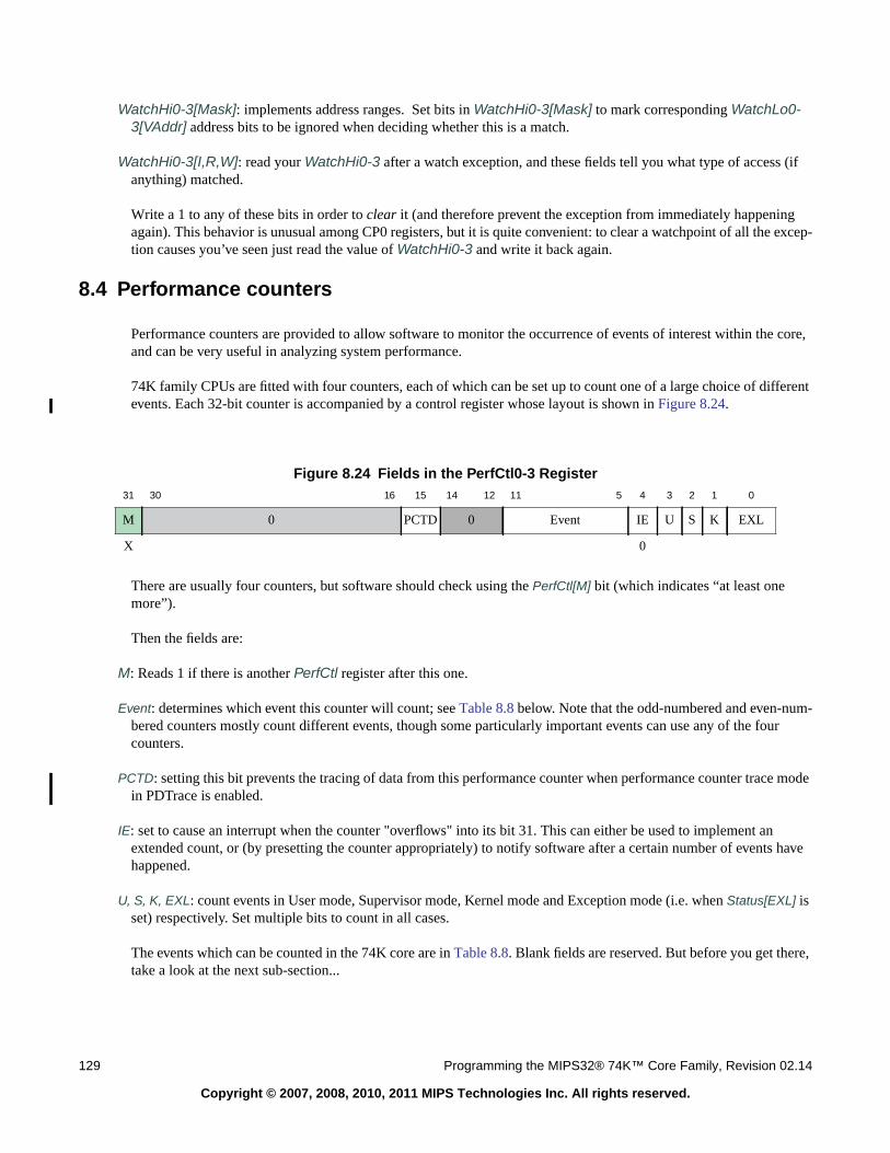
129 Programming the MIPS32® 74K™ Core Family, Revision 02.14
Copyright © 2007, 2008, 2010, 2011 MIPS Technologies Inc. All rights reserved.
WatchHi0-3[Mask]: implements address ranges. Set bits in WatchHi0-3[Mask] to mark corresponding WatchLo0-3[VAddr] address bits to be ignored when deciding whether this is a match.
WatchHi0-3[I,R,W]: read your WatchHi0-3 after a watch exception, and these fields tell you what type of access (ifanything) matched.
Write a 1 to any of these bits in order to clear it (and therefore prevent the exception from immediately happeningagain). This behavior is unusual among CP0 registers, but it is quite convenient: to clear a watchpoint of all the excep-tion causes you’ve seen just read the value of WatchHi0-3 and write it back again.
8.4 Performance counters
Performance counters are provided to allow software to monitor the occurrence of events of interest within the core,and can be very useful in analyzing system performance.
74K family CPUs are fitted with four counters, each of which can be set up to count one of a large choice of differentevents. Each 32-bit counter is accompanied by a control register whose layout is shown in Figure 8.24.
Figure 8.24 Fields in the PerfCtl0-3 Register
There are usually four counters, but software should check using the PerfCtl[M] bit (which indicates “at least onemore”).
Then the fields are:
M: Reads 1 if there is another PerfCtl register after this one.
Event: determines which event this counter will count; see Table 8.8 below. Note that the odd-numbered and even-num-bered counters mostly count different events, though some particularly important events can use any of the fourcounters.
PCTD: setting this bit prevents the tracing of data from this performance counter when performance counter trace modein PDTrace is enabled.
IE: set to cause an interrupt when the counter "overflows" into its bit 31. This can either be used to implement anextended count, or (by presetting the counter appropriately) to notify software after a certain number of events havehappened.
U, S, K, EXL: count events in User mode, Supervisor mode, Kernel mode and Exception mode (i.e. when Status[EXL] isset) respectively. Set multiple bits to count in all cases.
The events which can be counted in the 74K core are in Table 8.8. Blank fields are reserved. But before you get there,take a look at the next sub-section...
31 30 16 15 14 12 11 5 4 3 2 1 0
M 0 PCTD 0 Event IE U S K EXL
X 0
8.4 Performance counters
Programming the MIPS32® 74K™ Core Family, Revision 02.14 130
Copyright © 2007, 2008, 2010, 2011 MIPS Technologies Inc. All rights reserved.
8.4.1 Reading the event table.
There are a lot of events you can count. It’s relatively cheap to wire another signal from the internals of the core intoa counter. It’s time consuming and expensive to formulate a signal which represents exactly what a software engineermight want to count, and even more expensive to test it. Where the definitions in Table 8.8 are clear and simple,they’re usually exactly right. Where they seem more obscure, tread carefully, and don’t just blame the author of thismanual (though sometimes it is my fault!) When you use a counter, use it first on a piece of code where you know theanswer, and check you’re really counting what you think you are.
When reading the table:
• IFU: is the “instruction fetch unit” of the CPU pipeline. We can’t describe some events without referring to theinside of the CPU. You might like to look back at Section 1.4 “A brief guide to the 74K‘ core implementation”.
• LDQ, FSB, WBB: CPU queues, described in Section 3.3.1, "Read/write ordering and cache/memory data queuesin the 74K‘ core".
• Instruction fetch events: these include events in the I-cache, ITLB and main TLB (JTLB, for “joint TLB”, since itserves both I-fetches and data loads/stores). When you count these remember you are counting instructions at thestart of the pipeline — and there are many reasons why instructions are fetched but never executed (more pre-cisely, they never graduate):
• 74K CPUs have a 128-bit wide interface to the I-cache and fetch four instructions at once, so you only getone cache fetch for that group of four instructions. But even then, an unconditional branch which is not at theend of a group of four instructions means the remaining instructions will not be used: you can’t just multiplyI-cache fetches by four...
• When you get an exception all work started on instructions later in sequence than the exception victim is dis-carded: those instructions have been fetched and counted.
• The IFU's branch predictors cause it to fetch speculatively from a predicted branch target. When that turnsout to be wrong, those speculative instructions will be discarded.
If there's an exception-causing address error during I-fetch, that fetch won't be counted.
• Exceptions in a branch delay slot: are handled by internally setting the exception-return register EPC to point tothe branch instruction. After the exception is handled and control returns, the branch instruction is re-executed:all MIPS branch instructions are contrived so the re-execution does exactly the same thing as the first time. Butthe branch instruction is “really” run twice, and any performance count will show that.
• Bubble: is somewhat like a no-op, generated inside the execution unit. It travels down the pipeline like a realinstruction. When it reaches the pipeline position which is used by real instructions to access some resource, youcan be sure that resource will not be used for that cycle.
• Issue pool: this document’s informal name for the heap of instructions which are candidates for issue. Theseinstructions are kept in two 6-entry hardware queues which the implementation documents call DDQ0 andDDQ1 (for ALU and AGEN type instructions respectively).
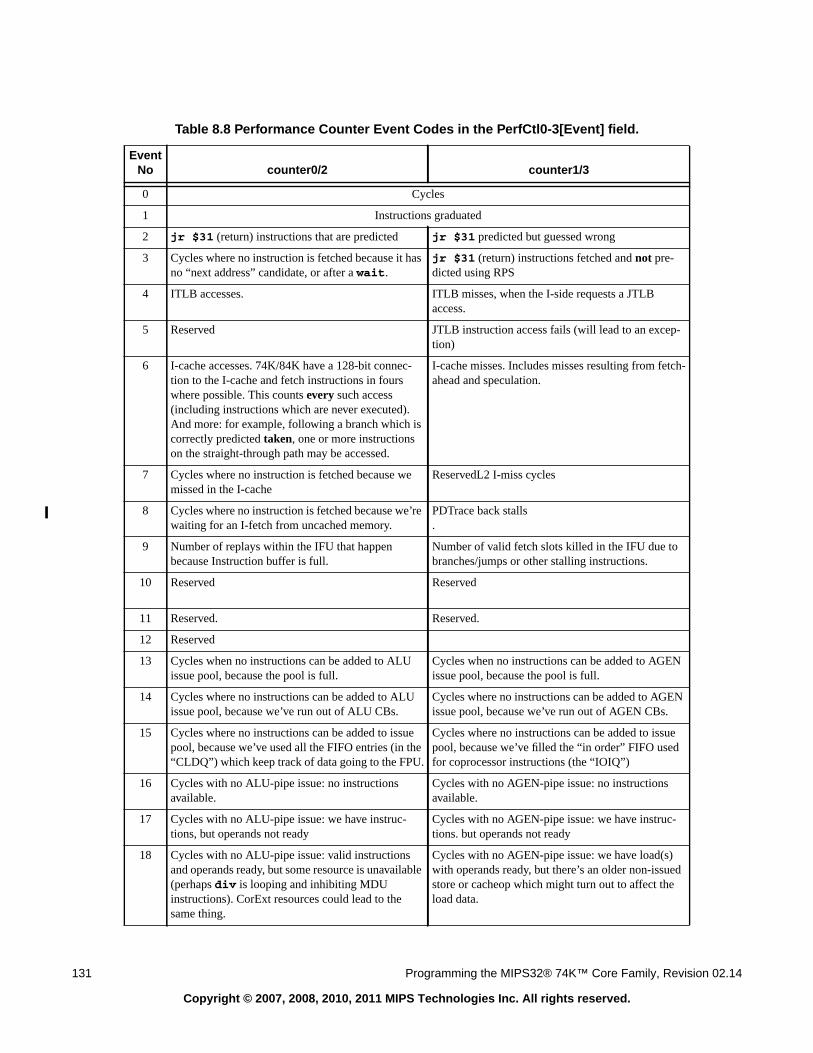
131 Programming the MIPS32® 74K™ Core Family, Revision 02.14
Copyright © 2007, 2008, 2010, 2011 MIPS Technologies Inc. All rights reserved.
Table 8.8 Performance Counter Event Codes in the PerfCtl0-3[Event] field.
EventNo counter0/2 counter1/3
0 Cycles
1 Instructions graduated
2 jr $31 (return) instructions that are predicted jr $31 predicted but guessed wrong
3 Cycles where no instruction is fetched because it hasno “next address” candidate, or after a wait.
jr $31 (return) instructions fetched and not pre-dicted using RPS
4 ITLB accesses. ITLB misses, when the I-side requests a JTLBaccess.
5 Reserved JTLB instruction access fails (will lead to an excep-tion)
6 I-cache accesses. 74K/84K have a 128-bit connec-tion to the I-cache and fetch instructions in fourswhere possible. This counts every such access(including instructions which are never executed).And more: for example, following a branch which iscorrectly predicted taken, one or more instructionson the straight-through path may be accessed.
I-cache misses. Includes misses resulting from fetch-ahead and speculation.
7 Cycles where no instruction is fetched because wemissed in the I-cache
ReservedL2 I-miss cycles
8 Cycles where no instruction is fetched because we’rewaiting for an I-fetch from uncached memory.
PDTrace back stalls.
9 Number of replays within the IFU that happenbecause Instruction buffer is full.
Number of valid fetch slots killed in the IFU due tobranches/jumps or other stalling instructions.
10 Reserved Reserved
11 Reserved. Reserved.
12 Reserved
13 Cycles when no instructions can be added to ALUissue pool, because the pool is full.
Cycles when no instructions can be added to AGENissue pool, because the pool is full.
14 Cycles where no instructions can be added to ALUissue pool, because we’ve run out of ALU CBs.
Cycles where no instructions can be added to AGENissue pool, because we’ve run out of AGEN CBs.
15 Cycles where no instructions can be added to issuepool, because we’ve used all the FIFO entries (in the“CLDQ”) which keep track of data going to the FPU.
Cycles where no instructions can be added to issuepool, because we’ve filled the “in order” FIFO usedfor coprocessor instructions (the “IOIQ”)
16 Cycles with no ALU-pipe issue: no instructionsavailable.
Cycles with no AGEN-pipe issue: no instructionsavailable.
17 Cycles with no ALU-pipe issue: we have instruc-tions, but operands not ready
Cycles with no AGEN-pipe issue: we have instruc-tions. but operands not ready
18 Cycles with no ALU-pipe issue: valid instructionsand operands ready, but some resource is unavailable(perhaps div is looping and inhibiting MDUinstructions). CorExt resources could lead to thesame thing.
Cycles with no AGEN-pipe issue: we have load(s)with operands ready, but there’s an older non-issuedstore or cacheop which might turn out to affect theload data.
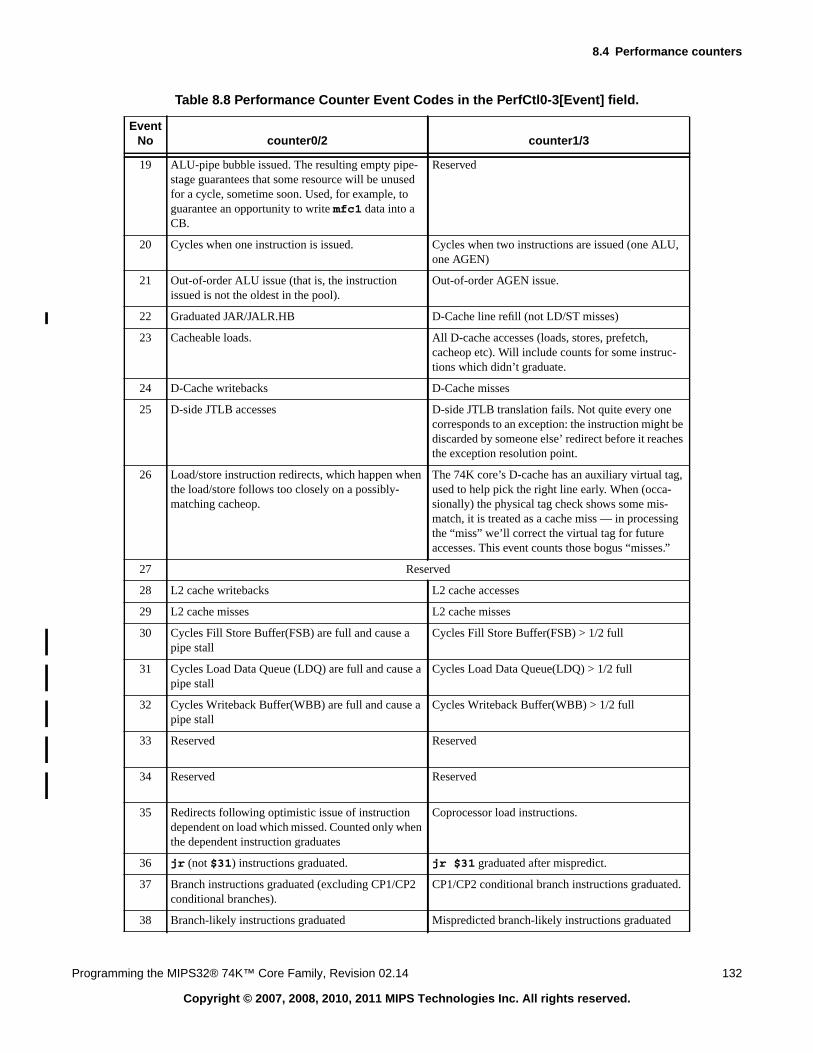
8.4 Performance counters
Programming the MIPS32® 74K™ Core Family, Revision 02.14 132
Copyright © 2007, 2008, 2010, 2011 MIPS Technologies Inc. All rights reserved.
19 ALU-pipe bubble issued. The resulting empty pipe-stage guarantees that some resource will be unusedfor a cycle, sometime soon. Used, for example, toguarantee an opportunity to write mfc1 data into aCB.
Reserved
20 Cycles when one instruction is issued. Cycles when two instructions are issued (one ALU,one AGEN)
21 Out-of-order ALU issue (that is, the instructionissued is not the oldest in the pool).
Out-of-order AGEN issue.
22 Graduated JAR/JALR.HB D-Cache line refill (not LD/ST misses)
23 Cacheable loads. All D-cache accesses (loads, stores, prefetch,cacheop etc). Will include counts for some instruc-tions which didn’t graduate.
24 D-Cache writebacks D-Cache misses
25 D-side JTLB accesses D-side JTLB translation fails. Not quite every onecorresponds to an exception: the instruction might bediscarded by someone else’ redirect before it reachesthe exception resolution point.
26 Load/store instruction redirects, which happen whenthe load/store follows too closely on a possibly-matching cacheop.
The 74K core’s D-cache has an auxiliary virtual tag,used to help pick the right line early. When (occa-sionally) the physical tag check shows some mis-match, it is treated as a cache miss — in processingthe “miss” we’ll correct the virtual tag for futureaccesses. This event counts those bogus “misses.”
27 Reserved
28 L2 cache writebacks L2 cache accesses
29 L2 cache misses L2 cache misses
30 Cycles Fill Store Buffer(FSB) are full and cause apipe stall
Cycles Fill Store Buffer(FSB) > 1/2 full
31 Cycles Load Data Queue (LDQ) are full and cause apipe stall
Cycles Load Data Queue(LDQ) > 1/2 full
32 Cycles Writeback Buffer(WBB) are full and cause apipe stall
Cycles Writeback Buffer(WBB) > 1/2 full
33 Reserved Reserved
34 Reserved Reserved
35 Redirects following optimistic issue of instructiondependent on load which missed. Counted only whenthe dependent instruction graduates
Coprocessor load instructions.
36 jr (not $31) instructions graduated. jr $31 graduated after mispredict.
37 Branch instructions graduated (excluding CP1/CP2conditional branches).
CP1/CP2 conditional branch instructions graduated.
38 Branch-likely instructions graduated Mispredicted branch-likely instructions graduated
Table 8.8 Performance Counter Event Codes in the PerfCtl0-3[Event] field.
EventNo counter0/2 counter1/3
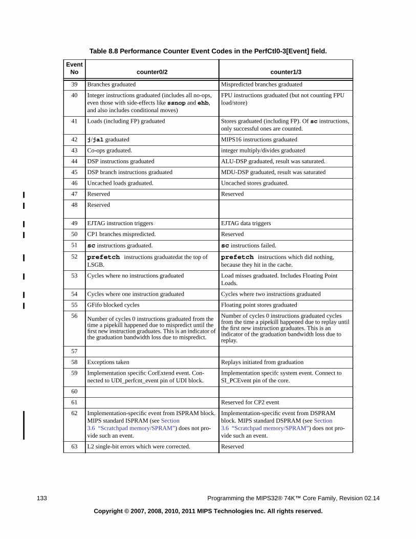
133 Programming the MIPS32® 74K™ Core Family, Revision 02.14
Copyright © 2007, 2008, 2010, 2011 MIPS Technologies Inc. All rights reserved.
39 Branches graduated Mispredicted branches graduated
40 Integer instructions graduated (includes all no-ops,even those with side-effects like ssnop and ehb,and also includes conditional moves)
FPU instructions graduated (but not counting FPUload/store)
41 Loads (including FP) graduated Stores graduated (including FP). Of sc instructions,only successful ones are counted.
42 j/jal graduated MIPS16 instructions graduated
43 Co-ops graduated. integer multiply/divides graduated
44 DSP instructions graduated ALU-DSP graduated, result was saturated.
45 DSP branch instructions graduated MDU-DSP graduated, result was saturated
46 Uncached loads graduated. Uncached stores graduated.
47 Reserved Reserved
48 Reserved
49 EJTAG instruction triggers EJTAG data triggers
50 CP1 branches mispredicted. Reserved
51 sc instructions graduated. sc instructions failed.
52 prefetch instructions graduatedat the top ofLSGB.
prefetch instructions which did nothing,because they hit in the cache.
53 Cycles where no instructions graduated Load misses graduated. Includes Floating PointLoads.
54 Cycles where one instruction graduated Cycles where two instructions graduated
55 GFifo blocked cycles Floating point stores graduated
56 Number of cycles 0 instructions graduated from thetime a pipekill happened due to mispredict until thefirst new instruction graduates. This is an indicator ofthe graduation bandwidth loss due to mispredict.
Number of cycles 0 instructions graduated cyclesfrom the time a pipekill happened due to replay untilthe first new instruction graduates. This is anindicator of the graduation bandwidth loss due toreplay.
57
58 Exceptions taken Replays initiated from graduation
59 Implementation specific CorExtend event. Con-nected to UDI_perfcnt_event pin of UDI block.
Implementation specifc system event. Connect toSI_PCEvent pin of the core.
60
61 Reserved for CP2 event
62 Implementation-specific event from ISPRAM block.MIPS standard ISPRAM (see Section3.6 “Scratchpad memory/SPRAM”) does not pro-vide such an event.
Implementation-specific event from DSPRAMblock. MIPS standard DSPRAM (see Section3.6 “Scratchpad memory/SPRAM”) does not pro-vide such an event.
63 L2 single-bit errors which were corrected. Reserved
Table 8.8 Performance Counter Event Codes in the PerfCtl0-3[Event] field.
EventNo counter0/2 counter1/3
8.4 Performance counters
Programming the MIPS32® 74K™ Core Family, Revision 02.14 134
Copyright © 2007, 2008, 2010, 2011 MIPS Technologies Inc. All rights reserved.
Appendix A
Programming the MIPS32® 74K™ Core Family, Revision 02.14 135
Copyright © 2007, 2008, 2010, 2011 MIPS Technologies Inc. All rights reserved.
References
74K™ core family manuals
[SUM]:“MIPS32® 74K® Processor Core Family Software User’s Manual”, MIPS Technologies document MD00519.
[ERRATA]:“MIPS32® 74K® Processor Core Family RTL Errata Sheet”, MIPS Technologies document MD00518.Available only to core licensees or by arrangement.
[INTGUIDE]:“MIPS32® 74K® Processor Core Family Integrator's Guide”, MIPS Technologies documentMD00499, available to core licensees, describes the options available with the core.
[CPS_USM]:“MIPS32® 74K® Coherent Processing System User’s Manual”, MIPS Technologies documentMD00597, available to core licensees, describes the other blocks within the CPS.
[74KC_DATA]:“MIPS32 74Kc™ Datasheet”, MIPS Technologies document MD00496.
[74KC_DATA]:“MIPS32 74Kc™ Datasheet”, MIPS Technologies document MD00496.
Other Manuals from MIPS Technologies
First of all, basic architectural documents.
[MIPS32]:The MIPS32 architecture definition series in three volumes:
[MIPS32V1]: “Introduction to the MIPS32 Architecture”, MIPS Technologies document MD00080.
[MIPS32V2]: “The MIPS32 Instruction Set”, MIPS Technologies document MD00084.
[MIPS32V3]: “The MIPS32 Privileged Resource Architecture”, MIPS Technologies document MD00088.
Although cores in the 74K family are 32-bit cores, the optional floating-point unit is a 64-bit one, and is as describedin:
[MIPS64V2]:“The MIPS64 Instruction Set”, MIPS Technologies document MD00085.
Then there are some architectural extensions:
[MIPSDSP]:“The MIPS DSP Application-Specific Extension to the MIPS32 Architecture”, MIPS Technologiesdocument MD00372.
[DSPWP]: “Programming the MIPS® 74K™ Family Cores for DSP”, MIPS Technologies white paper, documentnumber MD00544.
[MIPS16e]:“The MIPS16e™ Application-Specific Extension to the MIPS32 Architecture”, MIPS Technologiesdocument MD00074.
[CorExtend]:“How To Use CorExtend® User-Defined Instructions”, MIPS Technologies document MD00333.
[EJTAG]:“MIPS® EJTAG Specification”, MIPS Technologies document MD00047.
Programming the MIPS32® 74K™ Core Family, Revision 02.14 136
Copyright © 2007, 2008, 2010, 2011 MIPS Technologies Inc. All rights reserved.
[PDTRACEUSAGE]:“PDtrace™ and TCB Usage Guidelines”, MIPS Technologies document MD00365.
[PDTRACETCB]:“MIPS® PDtrace™ Interface and Trace Control Block Specification”, MIPS Technologiesdocument MD00439. Current revision is 4.30: you need revision 4 or greater to get multithreading trace information.[L2CACHE]:“MIPS® SOC-it® L2 Cache Controller Users Manual”, MIPS Technologies document MD00525.
Books about programming the MIPS® architecture
[SEEMIPSRUN]: “See MIPS Run, 2nd Edition”, author Dominic Sweetman, Morgan Kaufmann ISBN 1-55860-410-3. A general and wide-ranging programmers introduction to the MIPS architecture, updated in 2006 to reflect thecurrent version of [MIPS32].
[MIPSPROG]:“MIPS Programmers Handbook”, Erin Farquar & Philip Bunce, Morgan Kaufmann ISBN 1-55860-297-6. Restricted to the MIPS I instruction set but with a lot of assembler examples.
Other references
[IEEE754]:“IEEE Standard 754 for Binary Floating-Point Arithmetic”, published by the IEEE, widely available on theweb. Surprisingly comprehensible.
C language header files
Header files are available as part of the free-for-download “SDE Lite” subset available from MIPS Technologies’website. You’ll find them under.../sde/include/mips/. In particular:
[m32c0.h]:C definitions referred to in this manual for the names and fields of standard MIPS32 CP0 registers.
[m32tlb.h]:C definitions and constants associated with the basic address space and TLB programming.
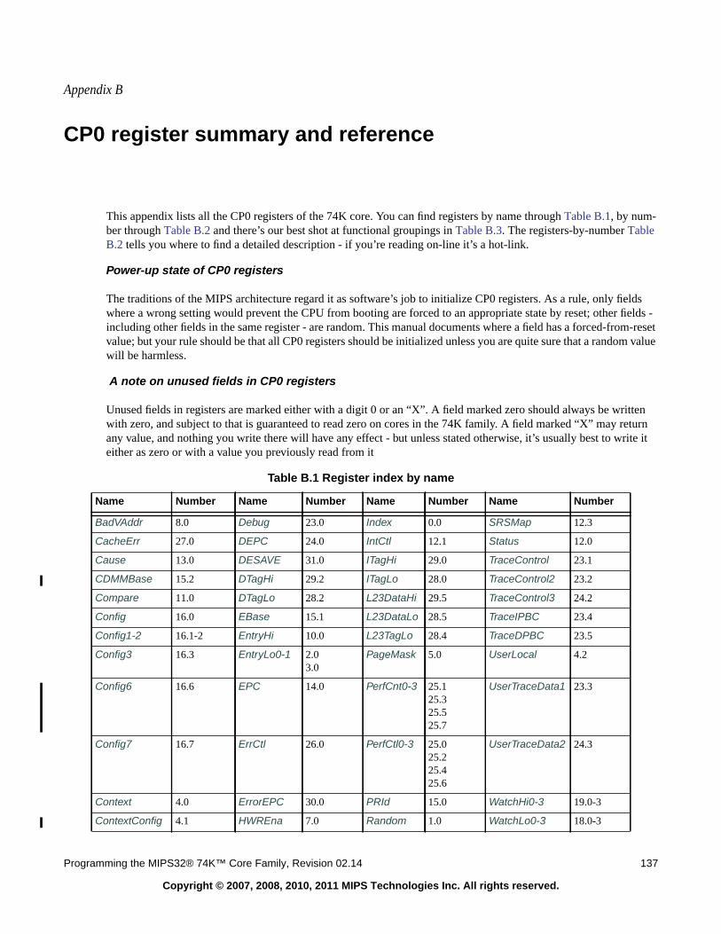
Appendix B
Programming the MIPS32® 74K™ Core Family, Revision 02.14 137
Copyright © 2007, 2008, 2010, 2011 MIPS Technologies Inc. All rights reserved.
CP0 register summary and reference
This appendix lists all the CP0 registers of the 74K core. You can find registers by name through Table B.1, by num-ber through Table B.2 and there’s our best shot at functional groupings in Table B.3. The registers-by-number TableB.2 tells you where to find a detailed description - if you’re reading on-line it’s a hot-link.
Power-up state of CP0 registers
The traditions of the MIPS architecture regard it as software’s job to initialize CP0 registers. As a rule, only fieldswhere a wrong setting would prevent the CPU from booting are forced to an appropriate state by reset; other fields -including other fields in the same register - are random. This manual documents where a field has a forced-from-resetvalue; but your rule should be that all CP0 registers should be initialized unless you are quite sure that a random valuewill be harmless.
A note on unused fields in CP0 registers
Unused fields in registers are marked either with a digit 0 or an “X”. A field marked zero should always be writtenwith zero, and subject to that is guaranteed to read zero on cores in the 74K family. A field marked “X” may returnany value, and nothing you write there will have any effect - but unless stated otherwise, it’s usually best to write iteither as zero or with a value you previously read from it
Table B.1 Register index by name
Name Number Name Number Name Number Name Number
BadVAddr 8.0 Debug 23.0 Index 0.0 SRSMap 12.3
CacheErr 27.0 DEPC 24.0 IntCtl 12.1 Status 12.0
Cause 13.0 DESAVE 31.0 ITagHi 29.0 TraceControl 23.1
CDMMBase 15.2 DTagHi 29.2 ITagLo 28.0 TraceControl2 23.2
Compare 11.0 DTagLo 28.2 L23DataHi 29.5 TraceControl3 24.2
Config 16.0 EBase 15.1 L23DataLo 28.5 TraceIPBC 23.4
Config1-2 16.1-2 EntryHi 10.0 L23TagLo 28.4 TraceDPBC 23.5
Config3 16.3 EntryLo0-1 2.03.0
PageMask 5.0 UserLocal 4.2
Config6 16.6 EPC 14.0 PerfCnt0-3 25.125.325.525.7
UserTraceData1 23.3
Config7 16.7 ErrCtl 26.0 PerfCtl0-3 25.025.225.425.6
UserTraceData2 24.3
Context 4.0 ErrorEPC 30.0 PRId 15.0 WatchHi0-3 19.0-3
ContextConfig 4.1 HWREna 7.0 Random 1.0 WatchLo0-3 18.0-3
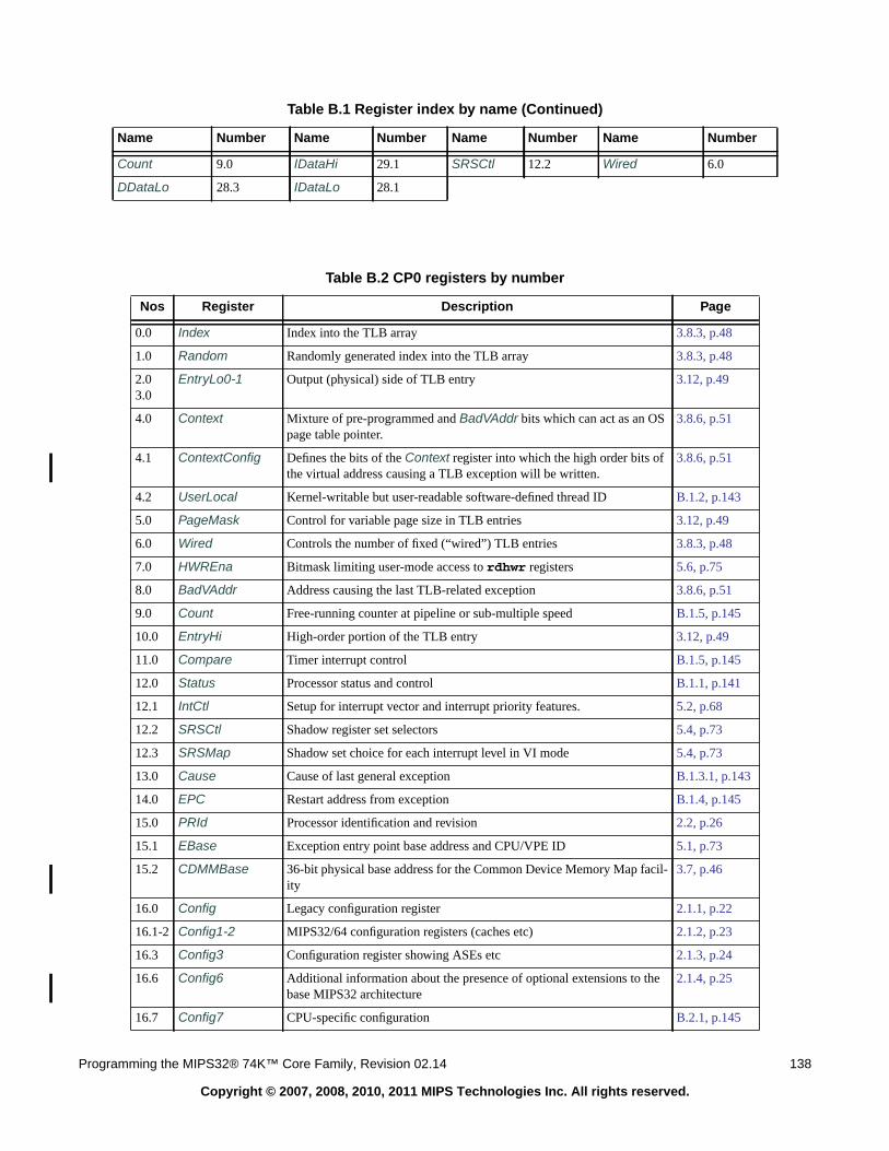
Programming the MIPS32® 74K™ Core Family, Revision 02.14 138
Copyright © 2007, 2008, 2010, 2011 MIPS Technologies Inc. All rights reserved.
Count 9.0 IDataHi 29.1 SRSCtl 12.2 Wired 6.0
DDataLo 28.3 IDataLo 28.1
Table B.2 CP0 registers by number
Nos Register Description Page
0.0 Index Index into the TLB array 3.8.3, p.48
1.0 Random Randomly generated index into the TLB array 3.8.3, p.48
2.03.0
EntryLo0-1 Output (physical) side of TLB entry 3.12, p.49
4.0 Context Mixture of pre-programmed and BadVAddr bits which can act as an OSpage table pointer.
3.8.6, p.51
4.1 ContextConfig Defines the bits of the Context register into which the high order bits ofthe virtual address causing a TLB exception will be written.
3.8.6, p.51
4.2 UserLocal Kernel-writable but user-readable software-defined thread ID B.1.2, p.143
5.0 PageMask Control for variable page size in TLB entries 3.12, p.49
6.0 Wired Controls the number of fixed (“wired”) TLB entries 3.8.3, p.48
7.0 HWREna Bitmask limiting user-mode access to rdhwr registers 5.6, p.75
8.0 BadVAddr Address causing the last TLB-related exception 3.8.6, p.51
9.0 Count Free-running counter at pipeline or sub-multiple speed B.1.5, p.145
10.0 EntryHi High-order portion of the TLB entry 3.12, p.49
11.0 Compare Timer interrupt control B.1.5, p.145
12.0 Status Processor status and control B.1.1, p.141
12.1 IntCtl Setup for interrupt vector and interrupt priority features. 5.2, p.68
12.2 SRSCtl Shadow register set selectors 5.4, p.73
12.3 SRSMap Shadow set choice for each interrupt level in VI mode 5.4, p.73
13.0 Cause Cause of last general exception B.1.3.1, p.143
14.0 EPC Restart address from exception B.1.4, p.145
15.0 PRId Processor identification and revision 2.2, p.26
15.1 EBase Exception entry point base address and CPU/VPE ID 5.1, p.73
15.2 CDMMBase 36-bit physical base address for the Common Device Memory Map facil-ity
3.7, p.46
16.0 Config Legacy configuration register 2.1.1, p.22
16.1-2 Config1-2 MIPS32/64 configuration registers (caches etc) 2.1.2, p.23
16.3 Config3 Configuration register showing ASEs etc 2.1.3, p.24
16.6 Config6 Additional information about the presence of optional extensions to thebase MIPS32 architecture
2.1.4, p.25
16.7 Config7 CPU-specific configuration B.2.1, p.145
Table B.1 Register index by name (Continued)
Name Number Name Number Name Number Name Number
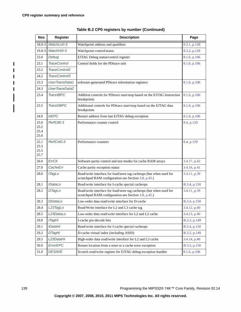
CP0 register summary and reference
139 Programming the MIPS32® 74K™ Core Family, Revision 02.14
Copyright © 2007, 2008, 2010, 2011 MIPS Technologies Inc. All rights reserved.
18.0-3 WatchLo0-3 Watchpoint address and qualifiers 8.3.1, p.128
19.0-3 WatchHi0-3 Watchpoint control/status 8.3.2, p.128
23.0 Debug EJTAG Debug status/control register 8.1.6, p.106
23.1 TraceControl Control fields for the PDtrace unit 8.1.6, p.106
23.2 TraceControl2
24.2 TraceControl3
23.3 UserTraceData1 software-generated PDtrace information registers 8.1.6, p.106
24.3 UserTraceData2
23.4 TraceIBPC Addition controls for PDtrace start/stop based on the EJTAG Instructionbreakpoints
8.1.6, p.106
23.5 TraceDBPC Additional controls for PDtrace start/stop based on the EJTAG databreakpoints
8.1.6, p.106
24.0 DEPC Restart address from last EJTAG debug exception 8.1.6, p.106
25.025.225.425.6
PerfCtl0-3 Performance counter control 8.4, p.129
25.125.325.525.7
PerfCnt0-3 Performance counters 8.4, p.129
26.0 ErrCtl Software parity control and test modes for cache RAM arrays 3.4.17, p.42
27.0 CacheErr Cache parity exception status 3.4.16, p.41
28.0 ITagLo Read/write interface for load/store tag cacheops (but when used forscratchpad RAM configuration see Section 3.8, p.45.)
3.4.11, p.39
28.1 IDataLo Read/write interface for I-cache special cacheops B.3.4, p.150
28.2 DTagLo Read/write interface for load/store tag cacheops (but when used forscratchpad RAM configuration see Section 3.8, p.45.)
3.4.11, p.39
28.3 DDataLo Low-order data read/write interface for D-cache B.3.4, p.150
28.4 L23TagLo Read/Write interface for L2 and L3 cache tag 3.4.12, p.40
28.5 L23DataLo Low-order data read/write interface for L2 and L2 cache 3.4.13, p.40
29.0 ITagHi I-cache pre-decode bits B.3.3, p.149
29.1 IDataHi Read/write interface for I-cache special cacheops B.3.4, p.150
29.2 DTagHi D-cache virtual index (including ASID) B.3.2, p.149
29.5 L23DataHi High-order data read/write interface for L2 and L3 cache 3.4.14, p.40
30.0 ErrorEPC Restart location from a reset or a cache error exception B.3.5, p.150
31.0 DESAVE Scratch read/write register for EJTAG debug exception handler 8.1.6, p.106
Table B.2 CP0 registers by number (Continued)
Nos Register Description Page
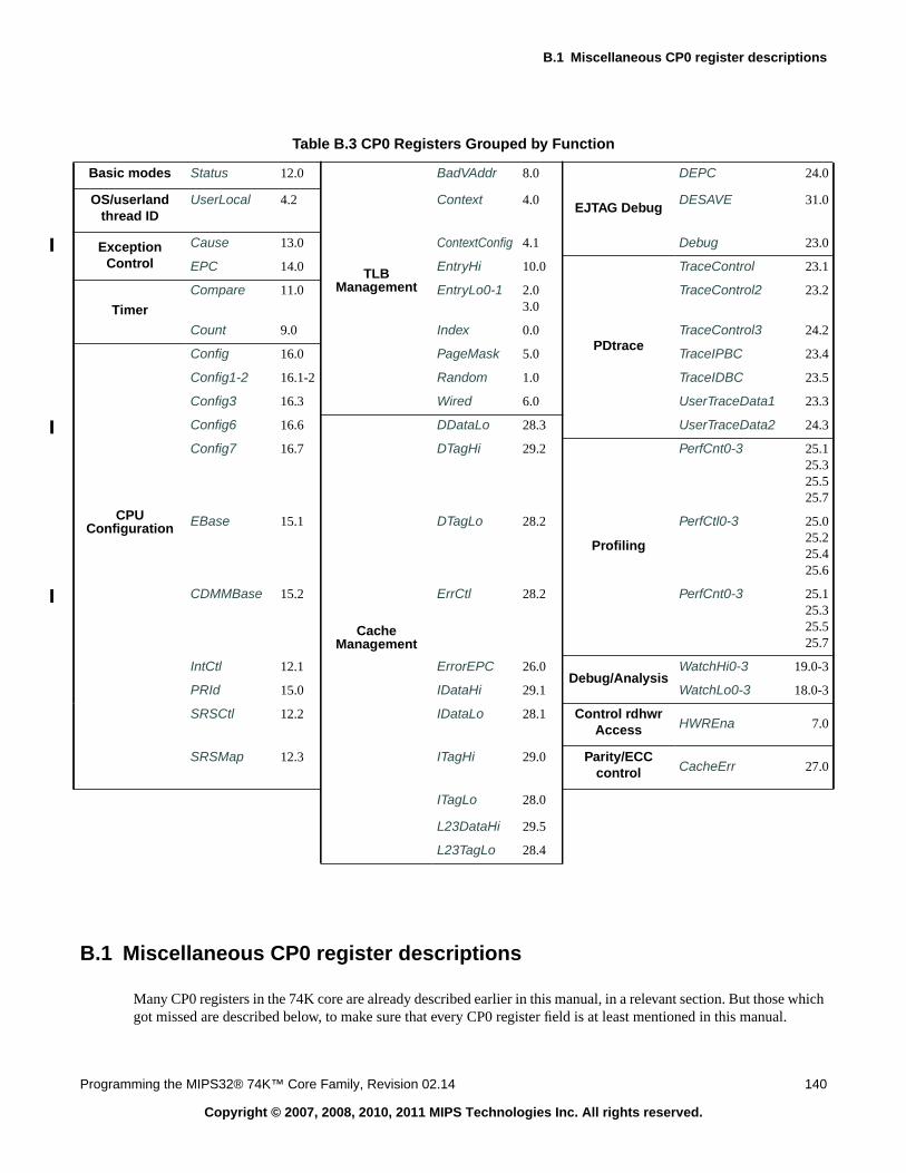
B.1 Miscellaneous CP0 register descriptions
Programming the MIPS32® 74K™ Core Family, Revision 02.14 140
Copyright © 2007, 2008, 2010, 2011 MIPS Technologies Inc. All rights reserved.
B.1 Miscellaneous CP0 register descriptions
Many CP0 registers in the 74K core are already described earlier in this manual, in a relevant section. But those whichgot missed are described below, to make sure that every CP0 register field is at least mentioned in this manual.
Table B.3 CP0 Registers Grouped by Function
Basic modes Status 12.0
TLBManagement
BadVAddr 8.0
EJTAG Debug
DEPC 24.0
OS/userlandthread ID
UserLocal 4.2 Context 4.0 DESAVE 31.0
ExceptionControl
Cause 13.0 ContextConfig 4.1 Debug 23.0
EPC 14.0 EntryHi 10.0
PDtrace
TraceControl 23.1
Timer
Compare 11.0 EntryLo0-1 2.03.0
TraceControl2 23.2
Count 9.0 Index 0.0 TraceControl3 24.2
CPUConfiguration
Config 16.0 PageMask 5.0 TraceIPBC 23.4
Config1-2 16.1-2 Random 1.0 TraceIDBC 23.5
Config3 16.3 Wired 6.0 UserTraceData1 23.3
Config6 16.6
CacheManagement
DDataLo 28.3 UserTraceData2 24.3
Config7 16.7 DTagHi 29.2
Profiling
PerfCnt0-3 25.125.325.525.7
EBase 15.1 DTagLo 28.2 PerfCtl0-3 25.025.225.425.6
CDMMBase 15.2 ErrCtl 28.2 PerfCnt0-3 25.125.325.525.7
IntCtl 12.1 ErrorEPC 26.0Debug/Analysis
WatchHi0-3 19.0-3
PRId 15.0 IDataHi 29.1 WatchLo0-3 18.0-3
SRSCtl 12.2 IDataLo 28.1 Control rdhwrAccess HWREna 7.0
SRSMap 12.3 ITagHi 29.0 Parity/ECCcontrol CacheErr 27.0
ITagLo 28.0
L23DataHi 29.5
L23TagLo 28.4
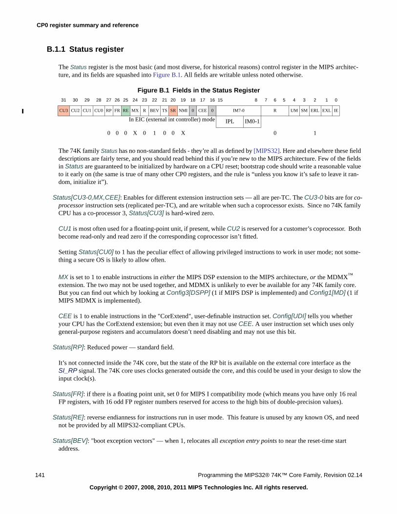
CP0 register summary and reference
141 Programming the MIPS32® 74K™ Core Family, Revision 02.14
Copyright © 2007, 2008, 2010, 2011 MIPS Technologies Inc. All rights reserved.
B.1.1 Status register
The Status register is the most basic (and most diverse, for historical reasons) control register in the MIPS architec-ture, and its fields are squashed into Figure B.1. All fields are writable unless noted otherwise.
Figure B.1 Fields in the Status Register
The 74K family Status has no non-standard fields - they’re all as defined by [MIPS32]. Here and elsewhere these fielddescriptions are fairly terse, and you should read behind this if you’re new to the MIPS architecture. Few of the fieldsin Status are guaranteed to be initialized by hardware on a CPU reset; bootstrap code should write a reasonable valueto it early on (the same is true of many other CP0 registers, and the rule is “unless you know it’s safe to leave it ran-dom, initialize it”).
Status[CU3-0,MX,CEE]: Enables for different extension instruction sets — all are per-TC. The CU3-0 bits are for co-processor instruction sets (replicated per-TC), and are writable when such a coprocessor exists. Since no 74K familyCPU has a co-processor 3, Status[CU3] is hard-wired zero.
CU1 is most often used for a floating-point unit, if present, while CU2 is reserved for a customer’s coprocessor. Bothbecome read-only and read zero if the corresponding coprocessor isn’t fitted.
Setting Status[CU0] to 1 has the peculiar effect of allowing privileged instructions to work in user mode; not some-thing a secure OS is likely to allow often.
MX is set to 1 to enable instructions in either the MIPS DSP extension to the MIPS architecture, or the MDMX™
extension. The two may not be used together, and MDMX is unlikely to ever be available for any 74K family core.But you can find out which by looking at Config3[DSPP] (1 if MIPS DSP is implemented) and Config1[MD] (1 ifMIPS MDMX is implemented).
CEE is 1 to enable instructions in the "CorExtend", user-definable instruction set. Config[UDI] tells you whetheryour CPU has the CorExtend extension; but even then it may not use CEE. A user instruction set which uses onlygeneral-purpose registers and accumulators doesn’t need disabling and may not use this bit.
Status[RP]: Reduced power — standard field.
It’s not connected inside the 74K core, but the state of the RP bit is available on the external core interface as theSI_RP signal. The 74K core uses clocks generated outside the core, and this could be used in your design to slow theinput clock(s).
Status[FR]: if there is a floating point unit, set 0 for MIPS I compatibility mode (which means you have only 16 realFP registers, with 16 odd FP register numbers reserved for access to the high bits of double-precision values).
Status[RE]: reverse endianness for instructions run in user mode. This feature is unused by any known OS, and neednot be provided by all MIPS32-compliant CPUs.
Status[BEV]: "boot exception vectors" — when 1, relocates all exception entry points to near the reset-time startaddress.
31 30 29 28 27 26 25 24 23 22 21 20 19 18 17 16 15 8 7 6 5 4 3 2 1 0
CU3 CU2 CU1 CU0 RP FR RE MX R BEV TS SR NMI 0 CEE 0 IM7-0 R UM SM ERL EXL IE
In EIC (external int controller) mode IPL IM0-1
0 0 0 X 0 1 0 0 X 0 1
B.1 Miscellaneous CP0 register descriptions
Programming the MIPS32® 74K™ Core Family, Revision 02.14 142
Copyright © 2007, 2008, 2010, 2011 MIPS Technologies Inc. All rights reserved.
Status[TS]: Set if software attempts to create a duplicate TLB entry (which will also produce a "machine check" excep-tion). Can be written back to zero, but never written to 1. The name of the field originated as a "TLB Shutdown" —historical MIPS CPUs quietly stopped translating addresses when they detected TLB abuse.
Status[SR]: MIPS32 architecture "soft reset" bit: the 74K core’s interface only supports a full external reset, so thisalways reads zero.
Status[NMI]: (read-only) — non-maskable interrupt shares the "reset" handler code, this field reads 1 when it was aNMI event which caused it.
Status[IM7-0]: bitwise interrupt enable for the eight interrupt conditions also visible in Cause[IP7-0], except in the"EIC" interrupt mode.
EIC mode is activated when Config3[VEIC] reads 1, and you set Cause[IV] and write a non-zero “vector spacing”into IntCtl[VS].
In EIC mode IM7-2 is recycled to become a 6-bit Status[IPL] (“interrupt priority level”) field. An interrupt is onlytriggered when your interrupt controller presents an interrupt code which is numerically higher than the current valueof Status[IPL].
Status[IM1-0] always act as bitwise masks for the two software interrupt bits programmable at Cause[IP1-0].
Status[UM,SM]: execution privilege level — basically user or kernel:
The intermediate “supervisor” privilege level is rarely used: but that’s why this is a 2-bit field.
Regardless of this field, the CPU is forced into kernel mode when either EXL or ERL is set.
Status[ERL,EXL]: EXL is the regular exception mode bit, set automatically when the CPU takes an exception. ERL isthe "error exception mode" bit, and is set following reset, an NMI, or a cache error exception. Either bit forces kernelmode and disables interrupts.
There are some very special cases where nested exceptions are permitted, so an exception with EXL set does severalstrange things: a nested TLB Refill exception is sent to the general exception handler (not, as is usual, it’s dedicatedentry point), and on a nested exception EPC, Cause[BD] and SRSCtl are not overwritten. The result, broadly, is thatwhen you return from the second exception you skip straight back to the code which was running before the first. Formore details see [SEEMIPSRUN] or the [MIPS32] bible.
The error level has its own return address: when ERL is set the eret instruction gets its address from ErrorEPC, notEPC as normal.
Moreover, error level changes the memory map (in support of software fixing up cache errors), recycling kuseg as anuncached, unmapped window onto 512MB of physical memory.
Table B.4 Encoding privilege level in Status[UM,SM]
UM SM Effect
0 0 kernel
0 1 supervisor
1 0 user
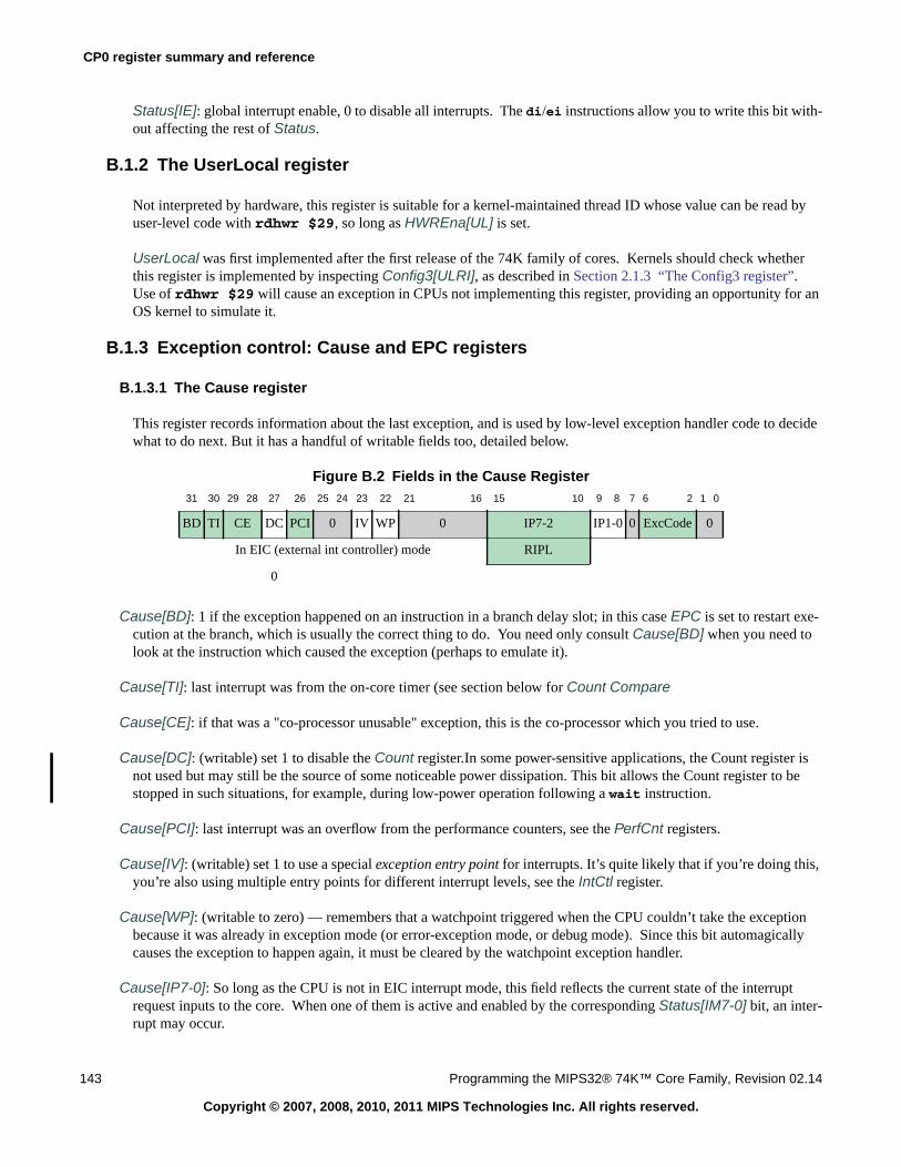
CP0 register summary and reference
143 Programming the MIPS32® 74K™ Core Family, Revision 02.14
Copyright © 2007, 2008, 2010, 2011 MIPS Technologies Inc. All rights reserved.
Status[IE]: global interrupt enable, 0 to disable all interrupts. The di/ei instructions allow you to write this bit with-out affecting the rest of Status.
B.1.2 The UserLocal register
Not interpreted by hardware, this register is suitable for a kernel-maintained thread ID whose value can be read byuser-level code with rdhwr $29, so long as HWREna[UL] is set.
UserLocal was first implemented after the first release of the 74K family of cores. Kernels should check whetherthis register is implemented by inspecting Config3[ULRI], as described in Section 2.1.3 “The Config3 register”.Use of rdhwr $29 will cause an exception in CPUs not implementing this register, providing an opportunity for anOS kernel to simulate it.
B.1.3 Exception control: Cause and EPC registers
B.1.3.1 The Cause register
This register records information about the last exception, and is used by low-level exception handler code to decidewhat to do next. But it has a handful of writable fields too, detailed below.
Figure B.2 Fields in the Cause Register
Cause[BD]: 1 if the exception happened on an instruction in a branch delay slot; in this case EPC is set to restart exe-cution at the branch, which is usually the correct thing to do. You need only consult Cause[BD] when you need tolook at the instruction which caused the exception (perhaps to emulate it).
Cause[TI]: last interrupt was from the on-core timer (see section below for Count Compare
Cause[CE]: if that was a "co-processor unusable" exception, this is the co-processor which you tried to use.
Cause[DC]: (writable) set 1 to disable the Count register.In some power-sensitive applications, the Count register isnot used but may still be the source of some noticeable power dissipation. This bit allows the Count register to bestopped in such situations, for example, during low-power operation following a wait instruction.
Cause[PCI]: last interrupt was an overflow from the performance counters, see the PerfCnt registers.
Cause[IV]: (writable) set 1 to use a special exception entry point for interrupts. It’s quite likely that if you’re doing this,you’re also using multiple entry points for different interrupt levels, see the IntCtl register.
Cause[WP]: (writable to zero) — remembers that a watchpoint triggered when the CPU couldn’t take the exceptionbecause it was already in exception mode (or error-exception mode, or debug mode). Since this bit automagicallycauses the exception to happen again, it must be cleared by the watchpoint exception handler.
Cause[IP7-0]: So long as the CPU is not in EIC interrupt mode, this field reflects the current state of the interruptrequest inputs to the core. When one of them is active and enabled by the corresponding Status[IM7-0] bit, an inter-rupt may occur.
31 30 29 28 27 26 25 24 23 22 21 16 15 10 9 8 7 6 2 1 0
BD TI CE DC PCI 0 IV WP 0 IP7-2 IP1-0 0 ExcCode 0
In EIC (external int controller) mode RIPL
0
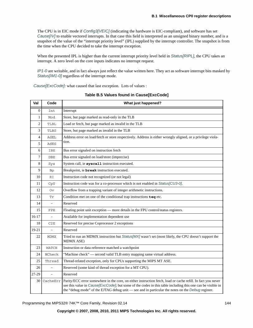
B.1 Miscellaneous CP0 register descriptions
Programming the MIPS32® 74K™ Core Family, Revision 02.14 144
Copyright © 2007, 2008, 2010, 2011 MIPS Technologies Inc. All rights reserved.
The CPU is in EIC mode if Config3[VEIC] (indicating the hardware is EIC-compliant), and software has setCause[IV] to enable vectored interrupts. In that case this field is interpreted as an unsigned binary number, and is asnapshot of the value of the “interrupt priority level” (IPL) supplied by the interrupt controller. The snapshot is fromthe time when the CPU decided to take the interrupt exception.
When the presented IPL is higher than the current interrupt priority level held in Status[RIPL], the CPU takes aninterrupt. A zero level on the core inputs indicates no interrupt request.
IP1-0 are writable, and in fact always just reflect the value written here. They act as software interrupt bits masked byStatus[IM1-0] regardless of the interrupt mode.
Cause[ExcCode]: what caused that last exception. Lots of values :
Table B.5 Values found in Cause[ExcCode]
Val Code What just happened?
0 Int Interrupt
1 Mod Store, but page marked as read-only in the TLB
2 TLBL Load or fetch, but page marked as invalid in the TLB
3 TLBS Store, but page marked as invalid in the TLB
4 AdEL Address error on load/fetch or store respectively. Address is either wrongly aligned, or a privilege viola-tion.5 AdES
6 IBE Bus error signaled on instruction fetch
7 DBE Bus error signaled on load/store (imprecise)
8 Sys System call, ie syscall instruction executed.
9 Bp Breakpoint, ie break instruction executed.
10 RI Instruction code not recognized (or not legal)
11 CpU Instruction code was for a co-processor which is not enabled in Status[CU3-0].
12 Ov Overflow from a trapping variant of integer arithmetic instructions.
13 Tr Condition met on one of the conditional trap instructions teq etc.
14 - Reserved
15 FPE Floating point unit exception — more details in the FPU control/status registers.
16-17 - Available for implementation dependent use
18 C2E Reserved for precise Coprocessor 2 exceptions
19-21 - Reserved
22 MDMX Tried to run an MDMX instruction but Status[MX] wasn’t set (most likely, the CPU doesn’t support theMDMX ASE)
23 WATCH Instruction or data reference matched a watchpoint
24 MCheck “Machine check” — second valid TLB entry mapping same virtual address.
25 Thread Thread-related exception, only for CPUs supporting the MIPS MT ASE.
26 - Reserved (some kind of thread exception for a MT CPU).
27-29 - Reserved
30 CacheErr Parity/ECC error somewhere in the core, on either instruction fetch, load or cache refill. In fact you neversee this value in Cause[ExcCode]; but some of the codes in this table including this one can be visible inthe “debug mode” of the EJTAG debug unit — see and in particular the notes on the Debug register.
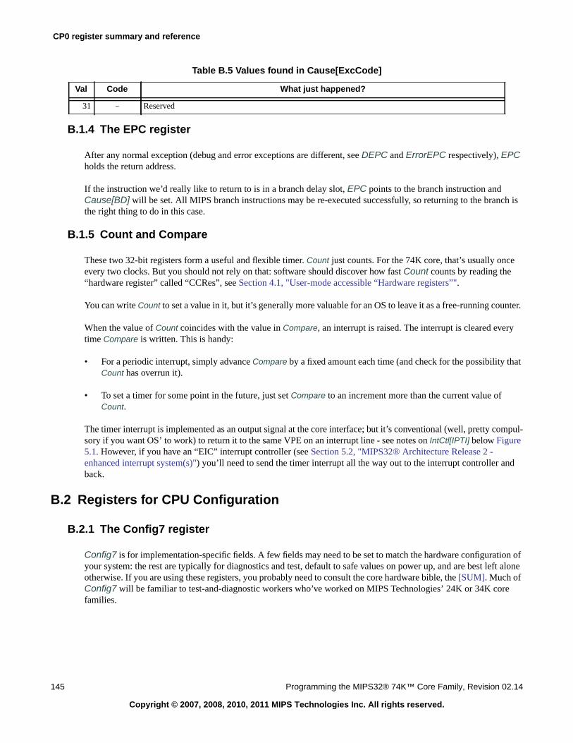
CP0 register summary and reference
145 Programming the MIPS32® 74K™ Core Family, Revision 02.14
Copyright © 2007, 2008, 2010, 2011 MIPS Technologies Inc. All rights reserved.
B.1.4 The EPC register
After any normal exception (debug and error exceptions are different, see DEPC and ErrorEPC respectively), EPCholds the return address.
If the instruction we’d really like to return to is in a branch delay slot, EPC points to the branch instruction andCause[BD] will be set. All MIPS branch instructions may be re-executed successfully, so returning to the branch isthe right thing to do in this case.
B.1.5 Count and Compare
These two 32-bit registers form a useful and flexible timer. Count just counts. For the 74K core, that’s usually onceevery two clocks. But you should not rely on that: software should discover how fast Count counts by reading the“hardware register” called “CCRes”, see Section 4.1, "User-mode accessible “Hardware registers”".
You can write Count to set a value in it, but it’s generally more valuable for an OS to leave it as a free-running counter.
When the value of Count coincides with the value in Compare, an interrupt is raised. The interrupt is cleared everytime Compare is written. This is handy:
• For a periodic interrupt, simply advance Compare by a fixed amount each time (and check for the possibility thatCount has overrun it).
• To set a timer for some point in the future, just set Compare to an increment more than the current value ofCount.
The timer interrupt is implemented as an output signal at the core interface; but it’s conventional (well, pretty compul-sory if you want OS’ to work) to return it to the same VPE on an interrupt line - see notes on IntCtl[IPTI] below Figure5.1. However, if you have an “EIC” interrupt controller (see Section 5.2, "MIPS32® Architecture Release 2 -enhanced interrupt system(s)") you’ll need to send the timer interrupt all the way out to the interrupt controller andback.
B.2 Registers for CPU Configuration
B.2.1 The Config7 register
Config7 is for implementation-specific fields. A few fields may need to be set to match the hardware configuration ofyour system: the rest are typically for diagnostics and test, default to safe values on power up, and are best left aloneotherwise. If you are using these registers, you probably need to consult the core hardware bible, the [SUM]. Much ofConfig7 will be familiar to test-and-diagnostic workers who’ve worked on MIPS Technologies’ 24K or 34K corefamilies.
31 - Reserved
Table B.5 Values found in Cause[ExcCode]
Val Code What just happened?
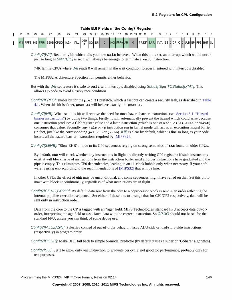
B.2 Registers for CPU Configuration
Programming the MIPS32® 74K™ Core Family, Revision 02.14 146
Copyright © 2007, 2008, 2010, 2011 MIPS Technologies Inc. All rights reserved.
Table B.6 Fields in the Config7 Register
Config7[WII]: Read-only bit which tells you how wait behaves. When this bit is set, an interrupt which would occurjust so long as Status[IE] is set 1 will always be enough to terminate a wait instruction.
74K family CPUs where WII reads 0 will remain in the wait condition forever if entered with interrupts disabled.
The MIPS32 Architecture Specification permits either behavior.
But with the WII-set feature it’s safe to wait with interrupts disabled using Status[IE]or TCStatus[IXMT]. Thisallows OS code to avoid a tricky race condition.
Config7[FPFS]: enable bit for the pref 31 prefetch, which is fast but can create a security leak, as described in Table4.1. When this bit isn’t set, pref 31 will behave exactly like pref 30.
Config7[IHB]: When set, this bit will remove the need for most hazard barrier instructions (see Section 5.1 “Hazardbarrier instructions”) by doing two things. Firstly, it will automatically prevent the hazard which could arise becauseone instruction produces a CP0 register value and a later instruction (which is one of mfc0, di, ei, eret or deret)consumes that value. Secondly, any jalr or jr instruction run in kernel mode will act as an execution hazard barrier(in fact, just like the corresponding jalr.hb or jr.hb). IHB is clear by default, which is fine so long as your codeinserts all the hazard barrier instructions required by [MIPS32].
Config7[SEHB]: "Slow EHB": mode to fix CP0 sequences relying on strong semantics of ehb found on older CPUs.
By default, ehb will check whether any instructions in flight are directly writing CP0 registers: if such instructionsexist, it will block issue of instructions from the instruction buffer until all older instructions have graduated and thepipe is empty. This eliminates CP0 dependencies, leading to an 11-clock bubble only when necessary. If your soft-ware is using ehb according to the recommendations of [MIPS32] that will be fine.
In other CPUs the effect of ehb may be unconditional, and some sequences might have relied on that. Set this bit tomake ehb block unconditionally, regardless of what instructions are in flight.
Config7[CP1IO,CP2IO]: By default data sent from the core to a coprocessor block is sent in an order reflecting theinternal pipeline execution sequence. Set either of these bits to arrange that for CP1/CP2 respectively, data will besent only in instruction order.
Data from the core to the CP is tagged with an “age” field. MIPS Technologies' standard FPU accepts data out-of-order, interpreting the age field to associated data with the correct instruction. So CP1IO should not be set for thestandard FPU, unless you can think of some debug use.
Config7[IALU,IAGN]: Selective control of out-of-order behavior: issue ALU-side or load/store-side instructions(respectively) in program order.
Config7[DGHR]: Make BHT fall back to simple bi-modal predictor (by default it uses a superior "GShare" algorithm).
Config7[SG]: Set 1 to allow only one instruction to graduate per cycle: not good for performance, probably only fortest purposes.
31 30 29 28 27 26 25 24 23 22 21 20 19 18 17 16 15 13 12 11 10 9 8 7 6 5 4 3 2 1 0
WII FPFS IHB FPR1 SEHB CP2IO IAGN IALUDGH
RSG SUI 0 HCI FPR0 AR 0 PREF IAR IVA ES 0 CP1IO 0 ULB BP RPS BHT SL
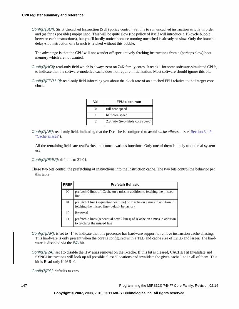
CP0 register summary and reference
147 Programming the MIPS32® 74K™ Core Family, Revision 02.14
Copyright © 2007, 2008, 2010, 2011 MIPS Technologies Inc. All rights reserved.
Config7[SUI]: Strict Uncached Instruction (SUI) policy control. Set this to run uncached instruction strictly in orderand (as far as possible) unpipelined. This will be quite slow (the policy of itself will introduce a 15-cycle bubblebetween each instructions), but you’ll hardly notice because running uncached is already so slow. Only the branch-delay-slot instruction of a branch is fetched without this bubble.
The advantage is that the CPU will not wander off speculatively fetching instructions from a (perhaps slow) bootmemory which are not wanted.
Config7[HCI]: read-only field which is always zero on 74K family cores. It reads 1 for some software-simulated CPUs,to indicate that the software-modelled cache does not require initialization. Most software should ignore this bit.
Config7[FPR1-0]: read-only field informing you about the clock rate of an attached FPU relative to the integer coreclock:
Config7[AR]: read-only field, indicating that the D-cache is configured to avoid cache aliases — see Section 3.4.9,"Cache aliases").
All the remaining fields are read/write, and control various functions. Only one of them is likely to find real systemuse:
Config7[PREF]: defaults to 2’b01.
These two bits control the prefetching of instructions into the Instruction cache. The two bits control the behavior perthis table:
Config7[IAR]: is set to “1” to indicate that this processor has hardware support to remove instruction cache aliasing.This hardware is only present when the core is configured with a TLB and cache size of 32KB and larger. The hard-ware is disabled via the IVA bit.
Config7[IVA]: set 1to disable the HW alias removal on the I-cache. If this bit is cleared, CACHE Hit Invalidate andSYNCI instructions will look up all possible aliased locations and invalidate the given cache line in all of them. Thisbit is Read-only if IAR=0.
Config7[ES]: defaults to zero.
Val FPU clock rate
0 full core speed
1 half core speed
2 2:3 ratio (two-thirds core speed)
PREF Prefetch Behavior
00 prefetch 0 lines of ICache on a miss in addition to fetching the missedline
01 prefetch 1 line (sequential next line) of ICache on a miss in addition tofetching the missed line (default behavior)
10 Reserved
11 prefetch 2 lines (seqeuntial next 2 lines) of ICache on a miss in additionto fetching the missed line
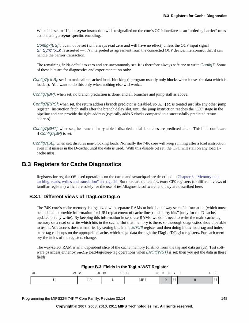
B.3 Registers for Cache Diagnostics
Programming the MIPS32® 74K™ Core Family, Revision 02.14 148
Copyright © 2007, 2008, 2010, 2011 MIPS Technologies Inc. All rights reserved.
When it is set to “1”, the sync instruction will be signalled on the core’s OCP interface as an “ordering barrier” trans-action, using a sync-specific encoding.
Config7[ES] bit cannot be set (will always read zero and will have no effect) unless the OCP input signalSI_SyncTxEn is asserted — it’s interpreted as agreement from the connected OCP device/interconnect that it canhandle the barrier transaction.
The remaining fields default to zero and are uncommonly set. It is therefore always safe not to write Config7. Someof these bits are for diagnostics and experimentation only:
Config7[ULB]: set 1 to make all uncached loads blocking (a program usually only blocks when it uses the data which isloaded). You want to do this only when nothing else will work...
Config7[BP]: when set, no branch prediction is done, and all branches and jump stall as above.
Config7[RPS]: when set, the return address branch predictor is disabled, so jr $31 is treated just like any other jumpregister. Instruction fetch stalls after the branch delay slot, until the jump instruction reaches the "EX" stage in thepipeline and can provide the right address (typically adds 5 clocks compared to a successfully predicted returnaddress).
Config7[BHT]: when set, the branch history table is disabled and all branches are predicted taken. This bit is don’t careif Config7[BP] is set.
Config7[SL]: when set, disables non-blocking loads. Normally the 74K core will keep running after a load instructioneven if it misses in the D-cache, until the data is used. With this disable bit set, the CPU will stall on any load D-cache miss.
B.3 Registers for Cache Diagnostics
Registers for regular OS-used operations on the cache and scratchpad are described in Chapter 3, “Memory map,caching, reads, writes and translation” on page 29. But there are quite a few extra CP0 registers (or different views offamiliar registers) which are solely for the use of test/diagnostic software, and they are described here.
B.3.1 Different views of ITagLo/DTagLo
The 74K core’s cache memory is organized with separate RAMs to hold both “way select” information (which mustbe updated to provide information for LRU replacement of cache lines) and “dirty bits” (only for the D-cache,updated on any write). By keeping this information in separate RAMs, we don’t need to write the main cache tagmemory on a read or write which hits in the cache. But that memory is there, so thorough diagnostics should be ableto test it. You access these memories by setting bits in the ErrCtl register and then doing index-load-tag and index-store-tag cacheops on the appropriate cache, which stage data through the ITagLo/DTagLo registers. For each mem-ory the fields of the registers change.
The way-select RAM is an independent slice of the cache memory (distinct from the tag and data arrays). Test soft-ware ca access either by cache load-tag/store-tag operations when ErrCtl[WST] is set: then you get the data in thesefields.
Figure B.3 Fields in the TagLo-WST Register31 24 23 20 19 16 15 10 9 8 7 6 1 0
U LP L LRU 0 U 0 U
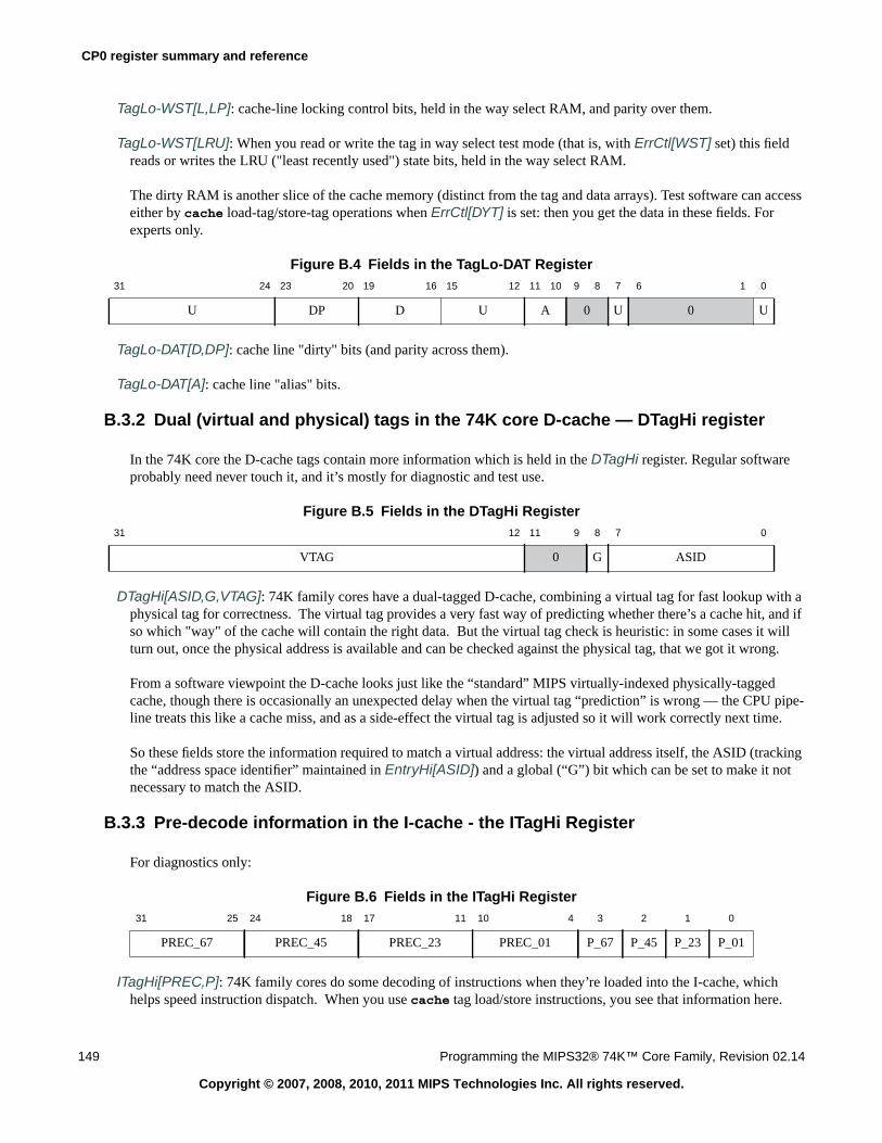
CP0 register summary and reference
149 Programming the MIPS32® 74K™ Core Family, Revision 02.14
Copyright © 2007, 2008, 2010, 2011 MIPS Technologies Inc. All rights reserved.
TagLo-WST[L,LP]: cache-line locking control bits, held in the way select RAM, and parity over them.
TagLo-WST[LRU]: When you read or write the tag in way select test mode (that is, with ErrCtl[WST] set) this fieldreads or writes the LRU ("least recently used") state bits, held in the way select RAM.
The dirty RAM is another slice of the cache memory (distinct from the tag and data arrays). Test software can accesseither by cache load-tag/store-tag operations when ErrCtl[DYT] is set: then you get the data in these fields. Forexperts only.
Figure B.4 Fields in the TagLo-DAT Register
TagLo-DAT[D,DP]: cache line "dirty" bits (and parity across them).
TagLo-DAT[A]: cache line "alias" bits.
B.3.2 Dual (virtual and physical) tags in the 74K core D-cache — DTagHi register
In the 74K core the D-cache tags contain more information which is held in the DTagHi register. Regular softwareprobably need never touch it, and it’s mostly for diagnostic and test use.
Figure B.5 Fields in the DTagHi Register
DTagHi[ASID,G,VTAG]: 74K family cores have a dual-tagged D-cache, combining a virtual tag for fast lookup with aphysical tag for correctness. The virtual tag provides a very fast way of predicting whether there’s a cache hit, and ifso which "way" of the cache will contain the right data. But the virtual tag check is heuristic: in some cases it willturn out, once the physical address is available and can be checked against the physical tag, that we got it wrong.
From a software viewpoint the D-cache looks just like the “standard” MIPS virtually-indexed physically-taggedcache, though there is occasionally an unexpected delay when the virtual tag “prediction” is wrong — the CPU pipe-line treats this like a cache miss, and as a side-effect the virtual tag is adjusted so it will work correctly next time.
So these fields store the information required to match a virtual address: the virtual address itself, the ASID (trackingthe “address space identifier” maintained in EntryHi[ASID]) and a global (“G”) bit which can be set to make it notnecessary to match the ASID.
B.3.3 Pre-decode information in the I-cache - the ITagHi Register
For diagnostics only:
Figure B.6 Fields in the ITagHi Register
ITagHi[PREC,P]: 74K family cores do some decoding of instructions when they’re loaded into the I-cache, whichhelps speed instruction dispatch. When you use cache tag load/store instructions, you see that information here.
31 24 23 20 19 16 15 12 11 10 9 8 7 6 1 0
U DP D U A 0 U 0 U
31 12 11 9 8 7 0
VTAG 0 G ASID
31 25 24 18 17 11 10 4 3 2 1 0
PREC_67 PREC_45 PREC_23 PREC_01 P_67 P_45 P_23 P_01
B.3 Registers for Cache Diagnostics
Programming the MIPS32® 74K™ Core Family, Revision 02.14 150
Copyright © 2007, 2008, 2010, 2011 MIPS Technologies Inc. All rights reserved.
The individual PREC fields hold precode information for pairs of adjacent instructions in the I-cache line, and the Pfields hold parity over them.
B.3.4 The DDataLo, IDataHi and IDataLo registers
On 74K family cores, test software can read or write data directly from/to the cache array using a cache index loadtag /store data instruction. Which word of the cache line is transferred depends on the low address fed to the cacheinstruction. D-cache load/stores transfer one word in DDataLo, but I-cache load/stores transfer two words in IDataHiand IDataLo. These are obscure and for-diagnostic-only operations on the cache array, but may be used when dealingwith scratchpad memory (see Section 3.6 “Scratchpad memory/SPRAM”).
B.3.5 The ErrorEPC register
This full 32-bit register is filled with the restart address on a cache error exception or any kind of CPU reset — in fact,any exception which sets Status[ERL] and leaves the CPU in “error mode”.
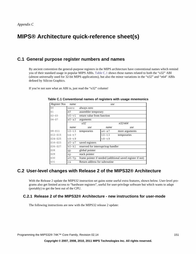
Appendix C
Programming the MIPS32® 74K™ Core Family, Revision 02.14 151
Copyright © 2007, 2008, 2010, 2011 MIPS Technologies Inc. All rights reserved.
MIPS® Architecture quick-reference sheet(s)
C.1 General purpose register numbers and names
By ancient convention the general-purpose registers in the MIPS architecture have conventional names which remindyou of their standard usage in popular MIPS ABIs. Table C.1 shows those names related to both the “o32” ABI(almost universally used for 32-bit MIPS applications), but also the minor variations in the “n32” and “n64” ABIsdefined by Silicon Graphics.
If you’re not sure what an ABI is, just read the “o32” column!
C.2 User-level changes with Release 2 of the MIPS32® Architecture
With the Release 2 update the MIPS32 instruction set gains some useful extra features, shown below. User-level pro-grams also get limited access to “hardware registers”, useful for user-privilege software but which wants to adapt(portably) to get the best out of the CPU.
C.2.1 Release 2 of the MIPS32® Architecture - new instructions for user-mode
The following instructions are new with the MIPS32 release 2 update:
Table C.1 Conventional names of registers with usage mnemonicsRegister Nos name use$0 zero always zero$1 AT assembler temporary$2-$3 v0-v1 return value from function$4-$7 a0-a3 arguments
o32 n32/n64name use name use
$8-$11 t0-t3 temporaries a4-a7 more arguments$12-$15 t4-t7 t0-t3 temporaries$24-$25 t8-t9 t8-t9$16-$23 s0-s7 saved registers$26-$27 k0-k1 reserved for interrupt/trap handler$28 gp global pointer$29 sp stack pointer$30 s8/fp frame pointer if needed (additional saved register if not)$31 ra Return address for subroutine
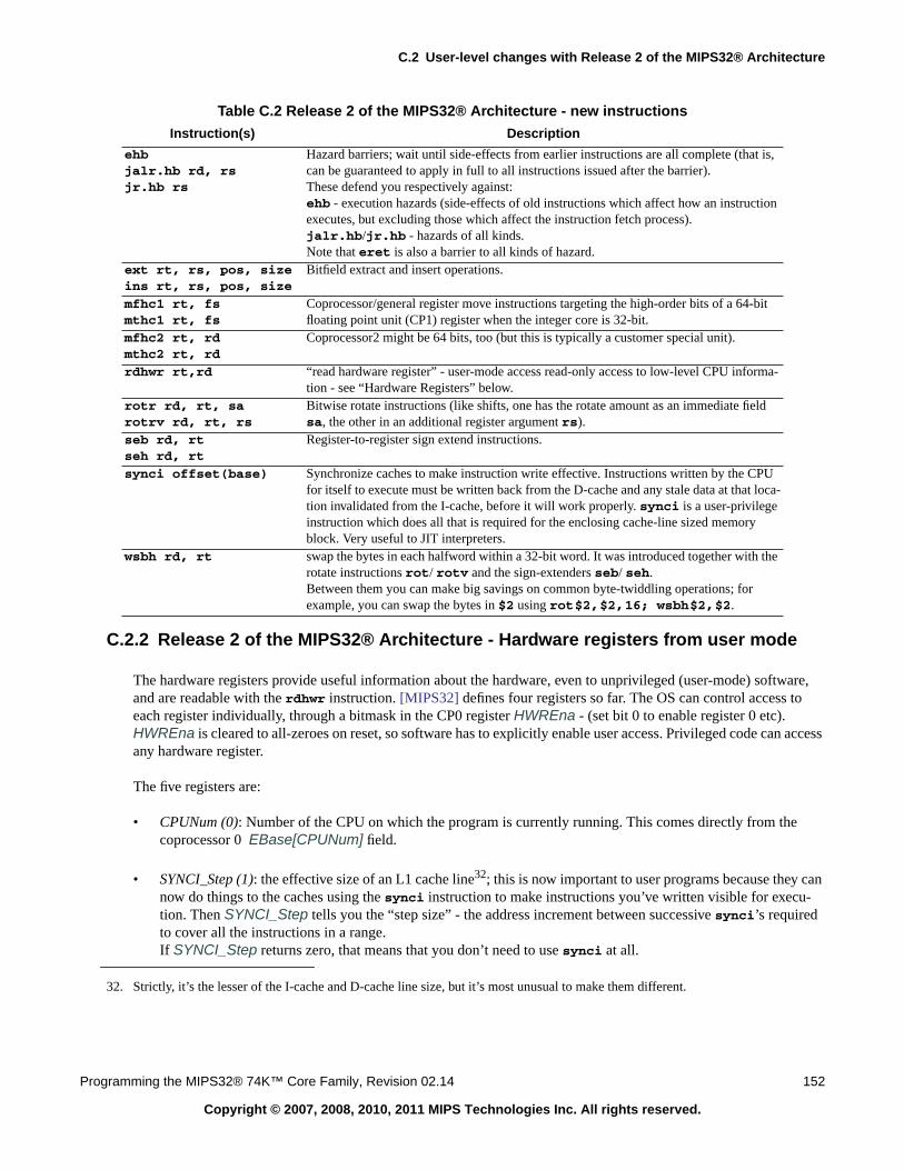
C.2 User-level changes with Release 2 of the MIPS32® Architecture
Programming the MIPS32® 74K™ Core Family, Revision 02.14 152
Copyright © 2007, 2008, 2010, 2011 MIPS Technologies Inc. All rights reserved.
C.2.2 Release 2 of the MIPS32® Architecture - Hardware registers from user mode
The hardware registers provide useful information about the hardware, even to unprivileged (user-mode) software,and are readable with the rdhwr instruction. [MIPS32] defines four registers so far. The OS can control access toeach register individually, through a bitmask in the CP0 register HWREna - (set bit 0 to enable register 0 etc).HWREna is cleared to all-zeroes on reset, so software has to explicitly enable user access. Privileged code can accessany hardware register.
The five registers are:
• CPUNum (0): Number of the CPU on which the program is currently running. This comes directly from thecoprocessor 0 EBase[CPUNum] field.
• SYNCI_Step (1): the effective size of an L1 cache line32; this is now important to user programs because they cannow do things to the caches using the synci instruction to make instructions you’ve written visible for execu-tion. Then SYNCI_Step tells you the “step size” - the address increment between successive synci’s requiredto cover all the instructions in a range.If SYNCI_Step returns zero, that means that you don’t need to use synci at all.
Table C.2 Release 2 of the MIPS32® Architecture - new instructionsInstruction(s) Description
ehbjalr.hb rd, rsjr.hb rs
Hazard barriers; wait until side-effects from earlier instructions are all complete (that is,can be guaranteed to apply in full to all instructions issued after the barrier).These defend you respectively against:ehb - execution hazards (side-effects of old instructions which affect how an instructionexecutes, but excluding those which affect the instruction fetch process).jalr.hb/jr.hb - hazards of all kinds.Note that eret is also a barrier to all kinds of hazard.
ext rt, rs, pos, sizeins rt, rs, pos, size
Bitfield extract and insert operations.
mfhc1 rt, fsmthc1 rt, fs
Coprocessor/general register move instructions targeting the high-order bits of a 64-bitfloating point unit (CP1) register when the integer core is 32-bit.
mfhc2 rt, rdmthc2 rt, rd
Coprocessor2 might be 64 bits, too (but this is typically a customer special unit).
rdhwr rt,rd “read hardware register” - user-mode access read-only access to low-level CPU informa-tion - see “Hardware Registers” below.
rotr rd, rt, sarotrv rd, rt, rs
Bitwise rotate instructions (like shifts, one has the rotate amount as an immediate fieldsa, the other in an additional register argument rs).
seb rd, rtseh rd, rt
Register-to-register sign extend instructions.
synci offset(base) Synchronize caches to make instruction write effective. Instructions written by the CPUfor itself to execute must be written back from the D-cache and any stale data at that loca-tion invalidated from the I-cache, before it will work properly. synci is a user-privilegeinstruction which does all that is required for the enclosing cache-line sized memoryblock. Very useful to JIT interpreters.
wsbh rd, rt swap the bytes in each halfword within a 32-bit word. It was introduced together with therotate instructions rot/ rotv and the sign-extenders seb/ seh.Between them you can make big savings on common byte-twiddling operations; forexample, you can swap the bytes in $2 using rot$2,$2,16; wsbh$2,$2.
32. Strictly, it’s the lesser of the I-cache and D-cache line size, but it’s most unusual to make them different.
MIPS® Architecture quick-reference sheet(s)
153 Programming the MIPS32® 74K™ Core Family, Revision 02.14
Copyright © 2007, 2008, 2010, 2011 MIPS Technologies Inc. All rights reserved.
• CC (2): user-mode read-only access to the CP0 Count register, for high-resolution counting. Which wouldn’t bemuch good without...
• CCRes (3): which tells you how fast Count counts. It’s a divider from the pipeline clock (if the rdhwr instructionreads a value of “2”, then Count increments every 2 cycles, at half the pipeline clock rate).
• UserLocal (29): Scratch register of sorts. The kernel can store a thread specific value such as a thread ID or apointer to thread specific storage to the underlying Cop0 register and user mode programs can read it via rdhwr
C.3 FPU changes in Release 2 of the MIPS32® Architecture
The main change is that a 32-bit CPU (like the 74K core) can now be paired with a 64-bit floating point unit. The FPUitself is compatible with the description in [MIPS64V2].
The only new feature of the instruction set are the mfhc1/mthc1 instructions described in Section C.2, "Release 2 ofthe MIPS32® Architecture - new instructions".
But it’s worth stressing that the floating point unit implements 64-bit load and store instructions. The FPU of the 74Kcore is described in Chapter 6, “Floating point unit” on page 77.
C.3 FPU changes in Release 2 of the MIPS32® Architecture
Programming the MIPS32® 74K™ Core Family, Revision 02.14 154
Copyright © 2007, 2008, 2010, 2011 MIPS Technologies Inc. All rights reserved.
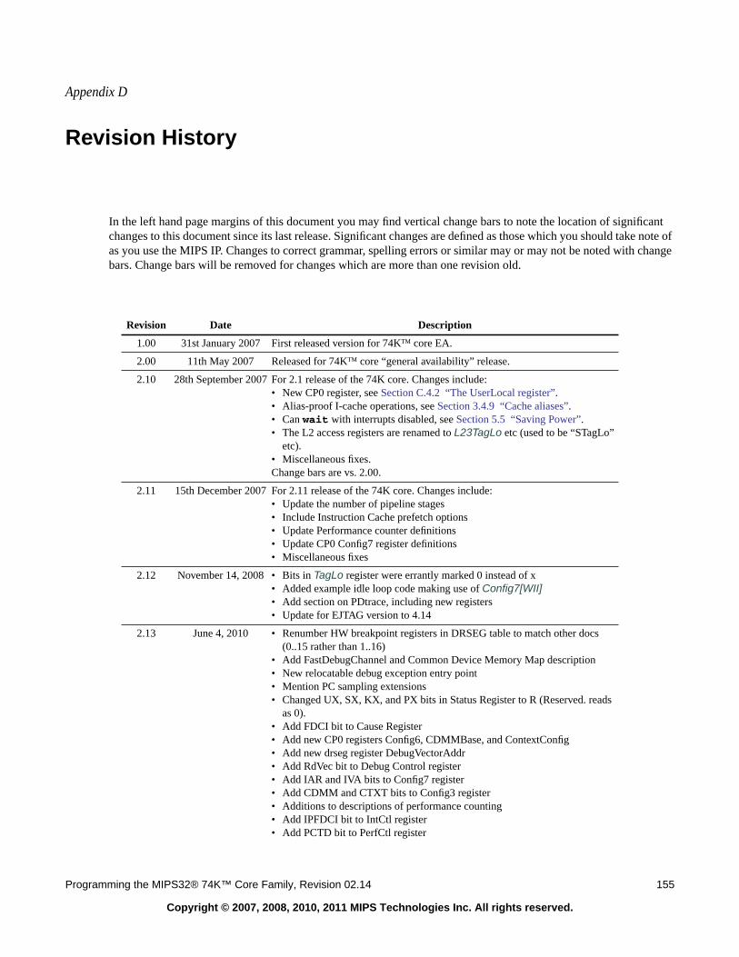
Appendix D
Programming the MIPS32® 74K™ Core Family, Revision 02.14 155
Copyright © 2007, 2008, 2010, 2011 MIPS Technologies Inc. All rights reserved.
Revision History
In the left hand page margins of this document you may find vertical change bars to note the location of significantchanges to this document since its last release. Significant changes are defined as those which you should take note ofas you use the MIPS IP. Changes to correct grammar, spelling errors or similar may or may not be noted with changebars. Change bars will be removed for changes which are more than one revision old.
Revision Date Description
1.00 31st January 2007 First released version for 74K™ core EA.
2.00 11th May 2007 Released for 74K™ core “general availability” release.
2.10 28th September 2007 For 2.1 release of the 74K core. Changes include:• New CP0 register, see Section C.4.2 “The UserLocal register”.• Alias-proof I-cache operations, see Section 3.4.9 “Cache aliases”.• Can wait with interrupts disabled, see Section 5.5 “Saving Power”.• The L2 access registers are renamed to L23TagLo etc (used to be “STagLo”
etc).• Miscellaneous fixes.Change bars are vs. 2.00.
2.11 15th December 2007 For 2.11 release of the 74K core. Changes include:• Update the number of pipeline stages• Include Instruction Cache prefetch options• Update Performance counter definitions• Update CP0 Config7 register definitions• Miscellaneous fixes
2.12 November 14, 2008 • Bits in TagLo register were errantly marked 0 instead of x• Added example idle loop code making use of Config7[WII]• Add section on PDtrace, including new registers• Update for EJTAG version to 4.14
2.13 June 4, 2010 • Renumber HW breakpoint registers in DRSEG table to match other docs(0..15 rather than 1..16)
• Add FastDebugChannel and Common Device Memory Map description• New relocatable debug exception entry point• Mention PC sampling extensions• Changed UX, SX, KX, and PX bits in Status Register to R (Reserved. reads
as 0).• Add FDCI bit to Cause Register• Add new CP0 registers Config6, CDMMBase, and ContextConfig• Add new drseg register DebugVectorAddr• Add RdVec bit to Debug Control register• Add IAR and IVA bits to Config7 register• Add CDMM and CTXT bits to Config3 register• Additions to descriptions of performance counting• Add IPFDCI bit to IntCtl register• Add PCTD bit to PerfCtl register
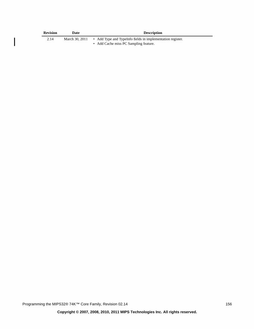
Programming the MIPS32® 74K™ Core Family, Revision 02.14 156
Copyright © 2007, 2008, 2010, 2011 MIPS Technologies Inc. All rights reserved.
2.14 March 30, 2011 • Add Type and TypeInfo fields in implementation register.• Add Cache miss PC Sampling feature.
Revision Date Description