Embed Size (px)
Citation preview
PROJECT FINAL REPORT
Grant Agreement number: 247868
Project acronym: e-LIFT
Project title: Laser printing of organic/inorganic material for the fabrication of electronic devices
Funding Scheme: Small or medium scale focused research project (STREP)
ICT-2009 3.3 a): Flexible, organic and/or large area electronic devices and building blocks
Period covered: from January 1st, 2010 to December 31st, 2012
Name of the scientific representative of the project's co-ordinator1, Title and Organisation:
Dr. DELAPORTE Philippe
Director of Research at CNRS
National Centre of the Scientific Research (CNRS)
Tel: 33 491 829 284
Fax: 33 491 829 289
E-mail: [email protected]
Project website address: http://www.e-lift-project.eu
1 Usually the contact person of the coordinator as specified in Art. 8.1. of the Grant Agreement.
1
TABLE OF CONTENTS
1. Executive summary 2
2. Description of project context and objectives 3
3. Main scientific and technical results 7
3.1. Optimization of LIFT process 7
3.1.1: LIFT of solids 7
3.3.2: LIFT of liquids 10
3.3.3: Printing complex structures 12
3.2. Application to printing PLEDs 13
3.3. Application to printing OTFTs 15
3.4. Application to printing sensors and biosensors 18
3.4.1: Chemical sensors for organic compounds based on chemical-selective
polymeric materials 20
3.4.2: Biosensors based on proteins 21
3.4.3: Gas sensor based on semiconducting oxide and/or catalyst 21
3.3.4: Electrochemical photosynthetic protein-based biosensors 22
3.5. Application to Energy harvesting 24
3.6. Printing new functions on RFID tags 27
3.7. Definition of a laser printing manufacturing tool 28
4. Potential impact and main dissemination activities 30
3.1. Potential impact of the project 30
4.2. Dissemination activities 35
5. e-LIFT Contacts and informations 39
2
1. Executive summary
The development of a simple process allowing the deposition of a wide variety of materials,
with high spatial resolution is of great interest for the manufacturing of future smart organic
electronic devices. The objective of the e-LIFT European project (FP7 ICT-2009 3.3) was to
demonstrate the integrability of a new laser process in the industrial world of electronic
device manufacturing for the localised deposition of organic and inorganic materials under
liquid or solid format.
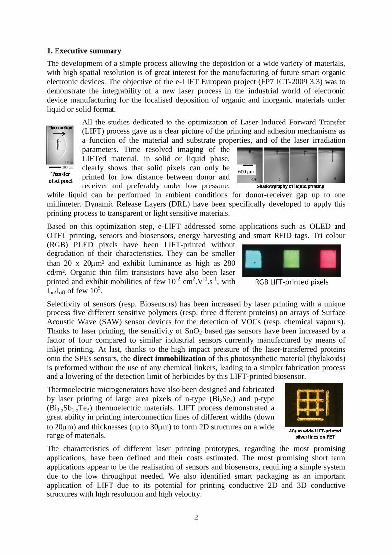
All the studies dedicated to the optimization of Laser-Induced Forward Transfer
(LIFT) process gave us a clear picture of the printing and adhesion mechanisms as
a function of the material and substrate properties, and of the laser irradiation
parameters. Time resolved imaging of the
LIFTed material, in solid or liquid phase,
clearly shows that solid pixels can only be
printed for low distance between donor and
receiver and preferably under low pressure,
while liquid can be performed in ambient conditions for donor-receiver gap up to one
millimeter. Dynamic Release Layers (DRL) have been specifically developed to apply this
printing process to transparent or light sensitive materials.
Based on this optimization step, e-LIFT addressed some applications such as OLED and
OTFT printing, sensors and biosensors, energy harvesting and smart RFID tags. Tri colour
(RGB) PLED pixels have been LIFT-printed without
degradation of their characteristics. They can be smaller
than 20 x 20m² and exhibit luminance as high as 280
cd/m². Organic thin film transistors have also been laser
printed and exhibit mobilities of few 10-2
cm2.V
-1.s
-1, with
Ion/Ioff of few 105.
Selectivity of sensors (resp. Biosensors) has been increased by laser printing with a unique
process five different sensitive polymers (resp. three different proteins) on arrays of Surface
Acoustic Wave (SAW) sensor devices for the detection of VOCs (resp. chemical vapours).
Thanks to laser printing, the sensitivity of SnO2 based gas sensors have been increased by a
factor of four compared to similar industrial sensors currently manufactured by means of
inkjet printing. At last, thanks to the high impact pressure of the laser-transferred proteins
onto the SPEs sensors, the direct immobilization of this photosynthetic material (thylakoids)
is preformed without the use of any chemical linkers, leading to a simpler fabrication process
and a lowering of the detection limit of herbicides by this LIFT-printed biosensor.
Thermoelectric microgenerators have also been designed and fabricated
by laser printing of large area pixels of n-type (Bi2Se3) and p-type
(Bi0.5Sb1.5Te3) thermoelectric materials. LIFT process demonstrated a
great ability in printing interconnection lines of different widths (down
to 20m) and thicknesses (up to 30m) to form 2D structures on a wide
range of materials.
The characteristics of different laser printing prototypes, regarding the most promising
applications, have been defined and their costs estimated. The most promising short term
applications appear to be the realisation of sensors and biosensors, requiring a simple system
due to the low throughput needed. We also identified smart packaging as an important
application of LIFT due to its potential for printing conductive 2D and 3D conductive
structures with high resolution and high velocity.
3
2. Description of project context and objectives
In the frame of the heterogeneous integration of organic devices, the development of a digital
printing process allowing the deposition of a wide variety of materials, with high spatial
resolution is of great interest for the manufacturing of future smart organic electronics. The
objective of the e-LIFT European project (FP7) is to demonstrate the integrability of a new
laser process in the industrial world of electronic device manufacturing for the localised
deposition of organic and inorganic materials under liquid or solid format.
The LIFT process is a laser-based technology enabling high resolution printing, in ambient
conditions, of a large set of materials, with typical sizes of a few micrometers. It has been
successfully applied so far in laboratory-scale trials for the deposition of organic and
inorganic compounds, polymers and biomaterials on various substrates.
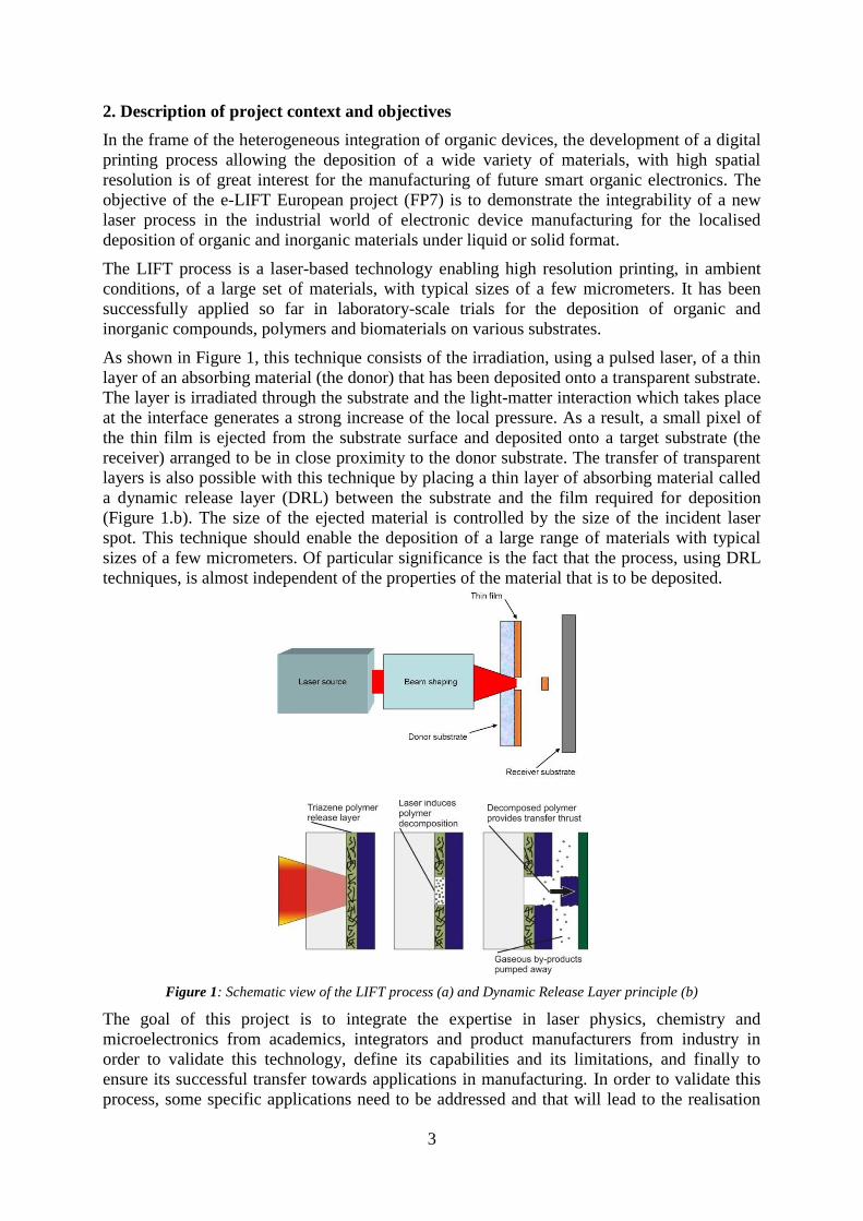
As shown in Figure 1, this technique consists of the irradiation, using a pulsed laser, of a thin
layer of an absorbing material (the donor) that has been deposited onto a transparent substrate.
The layer is irradiated through the substrate and the light-matter interaction which takes place
at the interface generates a strong increase of the local pressure. As a result, a small pixel of
the thin film is ejected from the substrate surface and deposited onto a target substrate (the
receiver) arranged to be in close proximity to the donor substrate. The transfer of transparent
layers is also possible with this technique by placing a thin layer of absorbing material called
a dynamic release layer (DRL) between the substrate and the film required for deposition
(Figure 1.b). The size of the ejected material is controlled by the size of the incident laser
spot. This technique should enable the deposition of a large range of materials with typical
sizes of a few micrometers. Of particular significance is the fact that the process, using DRL
techniques, is almost independent of the properties of the material that is to be deposited.
Figure 1: Schematic view of the LIFT process (a) and Dynamic Release Layer principle (b)
The goal of this project is to integrate the expertise in laser physics, chemistry and
microelectronics from academics, integrators and product manufacturers from industry in
order to validate this technology, define its capabilities and its limitations, and finally to
ensure its successful transfer towards applications in manufacturing. In order to validate this
process, some specific applications need to be addressed and that will lead to the realisation
4
and characterisation of single components such as TFT, OLED, sensors, energy harvesters,
and the laser printing of smart RFID tags.
The scientific and technical objectives of e-LIFT project are then divided in two parts:
a) Definition of a LIFT-based manufacturing tool
b) Realisation and characterisation of relevant organic devices
This first part aims to study of the LIFT mechanisms in order define the technical
specifications of a laser manufacturing tool. The optimization of the LIFT technique must
provide the process windows for the deposition of the different class of material of interest for
organic electronics. The capabilities and limitations of this printing technology (pixel size,
spatial resolution, multilayer deposition, and so on) will also be determined. One major
objective of the project is to develop a comprehensive suite of polymers for the dynamic layer
purpose. From this knowledge, the requirements and the technical solutions needed to develop
such a laser printing manufacturing tool will be defined. These activities include beam
shaping and manipulation, the remote motion of donor and receiver substrates, the surface
preparation for adhesion improvement, and the roll-to-roll compatibility. On top of this
general specifications, cost assessments and benchmarking will be undertaken for some niche
markets selected among the most pertinent for the LIFT process.
The second part of the e-LIFT project concerns the fabrication of organic/inorganic devices.
The selected applications are: OLEDs, OFETs, sensors, biosensors, energy harvesters and
adding new functions to standard RFID tags. The purpose of these work packages is not to
develop new products with exotic materials, but to demonstrate the ability of the LIFT process
to realize reliable and efficient standard products by depositing a large set of materials with a
simple and unique process. The performance of these LIFT-fabricated devices should be the
same or better that the performance obtained using other digital processes.
OLEDs. OLEDs are usually based on small light-emitting molecules (which at present for
pixelated display applications are mainly evaporated in high vacuum (HV) through shadow
masks). For three colour RGB displays, this complex and material-consuming deposition
process has to be sequentially repeated three times over, once for each colour. In this project,
we used electroluminescent polymers (ELPs) to print OLEDs. Due to the high molecular
weights of electroluminescent polymers evaporation/sublimation fails as a deposition method
for the fabrication of PLEDs. Therefore solvent-based or even "dry" printing techniques have
to be applied. Similar to OFETs, the state of the art OLEDs consist of a multilayer
architecture of typically between 4 and more than 7 well-defined layers (hole-injection, hole
transport, ELP, hole blocking, electron injection and separation layers plus anode and metal
cathode). The objectives of this study is to demonstrate the ability of the LIFT process to print
multilayer materials, including ELPs, in order to fabricate efficient PLEDs with pixel sizes
down to few micrometers (10m) and spatial resolution of one micrometer.
OTFT. The main purpose of this development is to demonstrate the advantages of not being
limited to solution-processed materials. The first step will be to define a reference by laser
printing an OFET with 'inkjet printable' organic materials (P3HT, PQT12) and compare the
results with those obtained by inkjet technology. The field mobility of such semiconducting
materials is around 10-3
– 10-2
cm²/ Vs. Then, the next step will be to take advantage of laser
printing process to deposit new set of organic material in order to realize OTFTs with higher
performances. Three configurations will be used to perform these studies: bottom gate (top
and bottom contacts) and top gate. The latter one is particularly challenging because our
objective is to transfer three layers in a single step (gate, oxide, semiconductor).
5
Sensors. In the field of chemical sensors most of the research work is concentrated towards
reducing the size of sensors and at identification and quantification of multiple species. Also,
good reversibility, sensitivity and selectivity are qualities also expected of an excellent sensor.
The field of applications of chemical sensors is very broad including quality and process
control, biomedical analysis, environmental control, etc. Four different types of sensors have
been selected to test the laser-printing process for its applicability to sensor fabrication.
Chemical sensors for organic compounds based on chemical-selective polymeric materials:
The combination of a nonselective transducer with chemoselective materials results in a
highly sensitive detector that responds selectively to a particular class of chemical vapors.
That’s currently a leading candidate for compact chemical vapor detection of volatile organic
compounds (VOCs) for environmental-monitoring applications. One of the most difficult
challenges is to find and print sensing materials that have good sensitivity and robust
selectivity to the substances to be detected. Conductive conjugated polymers are a relatively
new class of VOC sensing materials that show considerable promise to reach these goals.
First, their chemical composition is similar to VOCs, which may induce physical interactions
between sensing materials and analytes, leading to new sensing mechanisms. Second, their
chemical structures are readily modified, which enables custom material designs with specific
selectivity to target analytes. The LIFT process provides a unique opportunity to print, with
high resolution, and with limited risk of material damage, these multi-material arrays of
chemoselective sensors (SAW) in a unique and simple process.
Biosensors based on proteins: A biosensor comprises a biochemical recognition system and a
transducer which transforms the biochemical response into a measureable output signal. Thus
to permit the use of a SAW device as a biosensor, the device has to be coated with a
biospecific layer corresponding to the analyte. This concept has been successfully applied for
immunosensors, such as the immobilization of Anti-IgG on a quartz surface via silanization
and IgG as the analyte. The sensor designed in this project is based on the application of a
protein, i.e. Bovine Odorant-Binding Protein (bOBP), which allows the detection of boletus
mushroom taste. The protein is deposited from solution onto the active part of the SAW
sensor. LIFT can print this protein without risk of damaging it and with a very high spatial
resolution. The use of an array of proteins must allow the detection of a larger set of
biological species.
Gas sensor based on semiconducting oxide and/or catalyst: The integrated semiconductor and
catalytic gas sensors are currently realized on micro-heater structures. The well-known SnO2
semiconducting layer is sensitive to oxidizing and/or reducing gases at optimized temperature.
This material is used to produce sensors for combustible gas detection and for air quality
monitoring, detecting CO, NO2, VOC (Volatile Organic Compounds) in air. The present
technology used for depositing and structuring the gas-sensitive layers are either conventional
sputtering techniques with “lift-off” or “ink- jet” printing techniques. The thickness, the
porosity and the composition of doped oxides influence the sensitivity, the stability and the
selectivity of the sensor. For instance, the inkjet printing technique requires the preparation of
the sensitive material in a solvent solution, after which the material has to be sintered at high
temperature to ensure stability in device operation, and this operation induces a strong
reduction of the material sensitivity. The LIFT process is used to print the SnO2 layer without
such undesirable risk of material property deterioration. The performances of these laser
printed sensors will be compared to those of commercial sensors.
Electrochemical photosynthetic protein-based biosensors: Photosynthetic proteins are suitable
biological compounds for use as biomediators in biosensors, thanks to the electron transfer
and fluorescence emission properties. Thylakoil proteins have the ability to provide electrons
under light excitation. This is also a target site of the most widely used photosynthetic
6
pesticides. When pollutant molecules are added to the sample solution, they bind to them and
reduce or totally inhibit the electron transfer; consequently the current measured at the
amperometric biosensor output decreases as a function of the pesticide concentration. The
specific objectives of this study is the laser-deposition of first thylakoil proteins to compare
LIFT with other printing technologies, then the transfer of a biohybrid sensing material
(proteins in polymer) to improve the lifetime of the bioreceptor activity and enhance stability
and reproducibility of immobilization.
Energy harvesting. This application aims to demonstrate the ability of the LIFT process to
deposit films of complex materials in solid phase without loss of material properties. Energy-
harvesting is of great interest for nomadic products and energy optimisation. The deposition
of two kinds of materials has been studied. Piezoelectrics are used to convert mechanical
strain into useable electrical energy, while thermoelectric materials allow converting
temperature gradient in electricity. Laser printing of these materials will be performed to
realize microgenerators based on piezoelectric or thermoelectric effect. This activity is quite
challenging, because such materials are very brittle and the realization of efficient
microgenerators requires printing large area thick pixels (>1m).
Smart RFID tags. The realization of standard RFID tag is cost effective and do not require
new technology. However, the ability of printing personalized new functionalities of this
standard tags gives a high added value of the product and increase its field of applications. In
this context, LIFT has been used to print temperature sensors on standard RFID tags as well
as the connection lines to connect this new function to the pads of the tag.
Through these different studies, the overall objective of the project is to determine the most
pertinent applications for this new laser printing technology, both for its ability to print
specific material and its advantages for device fabrication.
7
3. Main scientific and technical results
3.1. Optimization of LIFT process
The optimization of the LIFT process has been done with selected materials and substrates
which are representative of the systems used in organic electronics and of the applications
targeted in the second part of the project. Then, the influences of the following experimental
parameters on the printing process have been investigated: pulse duration and wavelength of
the laser, surrounding gas pressure, distance between donor and receiver substrates and beam
energy profile.
Different in-situ and ex-situ analysis methods have been used to characterize the materials
before and after printing (SEM, EDX, confocal microscope, electrical measurement ...). A
special attention has been paid to study the hydrodynamics processes by means of time-
resolved fast imaging.
3.1.1. LIFT of solids
The materials investigated have been PEDOT, PQT, aluminum, PZT, SnO2, and the substrates
were aluminium, PET and SiO2.
a. Influence of irradiation parameters
Wavelength: Transfer of thin film requires the absorption of laser energy at the interface
between transparent substrate and film. When DRL is not used, proper wavelength selection is
required to ensure high radiation absorption. Printing with polymer DRL, like triazene (TP)
developed in the frame of this project, requires the use of wavelength below 220nm or in the
range 280 - 350nm. When femtosecond pulses are used, multi-photonic absorption of the
energy occurs and the influence of laser wavelength is strongly reduced
Pulse duration: Based on the morphological features of the printed pixels, we didn’t find that
the pulse duration was a key parameter for the LIFT process.
Laser fluence: This is a very important parameter for LIFT process, especially when DRL is
not used. Too low fluence does not allow a complete transfer of the layer, and too high
fluence leads to damaged pixels or debris generation. As a consequence, the deposition of a
uniform pixel requires a very uniform energy profile of the laser beam, typically with
fluctuations lower than 10%. Laser transfer with a polymer DRL allows reducing the
sensitivity of the process to this parameter, but the DRL thickness has to be tuned with the
film thickness.
b. Relation between surrounding gas pressure and donor - receiver distance
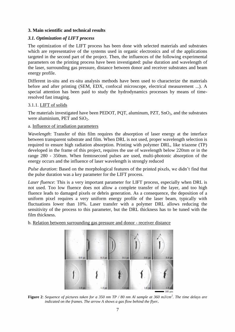
Figure 2: Sequence of pictures taken for a 350 nm TP / 80 nm Al sample at 360 mJ/cm
2. The time delays are
indicated on the frames. The arrow A shows a gas flow behind the flyer.
8
As shown on the figure 2, when the flyer is ejected from the donor substrate due to the laser
irradiation, its fast initial motion induces the generation of a shock wave which flows in front
of him. However, these images have been recorded without the presence of the receiver
substrate. When the receiver substrate is added, which represents the real situation, the shock
wave is reflected back onto it and destroys, or at least stops, the flyer which does not reach the
receiver. This process is clearly shown on figure 3.
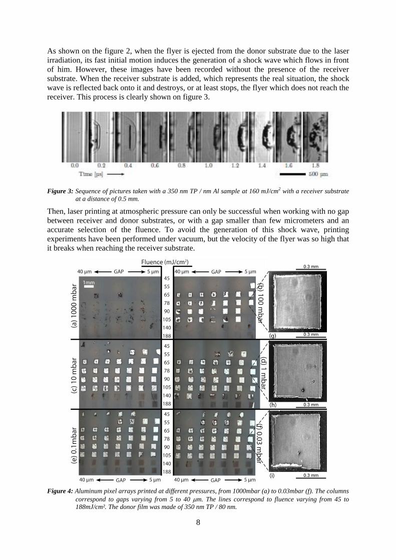
Figure 3: Sequence of pictures taken with a 350 nm TP / nm Al sample at 160 mJ/cm2 with a receiver substrate
at a distance of 0.5 mm.
Then, laser printing at atmospheric pressure can only be successful when working with no gap
between receiver and donor substrates, or with a gap smaller than few micrometers and an
accurate selection of the fluence. To avoid the generation of this shock wave, printing
experiments have been performed under vacuum, but the velocity of the flyer was so high that
it breaks when reaching the receiver substrate.
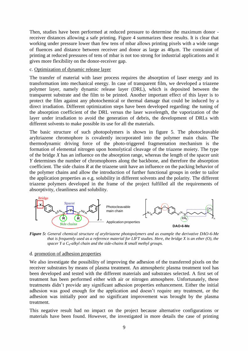
Figure 4: Aluminum pixel arrays printed at different pressures, from 1000mbar (a) to 0.03mbar (f). The columns
correspond to gaps varying from 5 to 40 m. The lines correspond to fluence varying from 45 to
188mJ/cm². The donor film was made of 350 nm TP / 80 nm.
9
Then, studies have been performed at reduced pressure to determine the maximum donor -
receiver distances allowing a safe printing. Figure 4 summarizes these results. It is clear that
working under pressure lower than few tens of mbar allows printing pixels with a wide range
of fluences and distance between receiver and donor as large as 40m. The constraint of
printing at reduced pressures of tens of mbar is not too strong for industrial applications and it
gives more flexibility on the donor-receiver gap.
c. Optimization of dynamic release layer
The transfer of material with laser process requires the absorption of laser energy and its
transformation into mechanical energy. In case of transparent film, we developed a triazene
polymer layer, namely dynamic release layer (DRL), which is deposited between the
transparent substrate and the film to be printed. Another important effect of this layer is to
protect the film against any photochemical or thermal damage that could be induced by a
direct irradiation. Different optimization steps have been developed regarding: the tuning of
the absorption coefficient of the DRL versus the laser wavelength, the vaporization of the
layer under irradiation to avoid the generation of debris, the development of DRLs with
different solvents to make possible its use for all the materials.
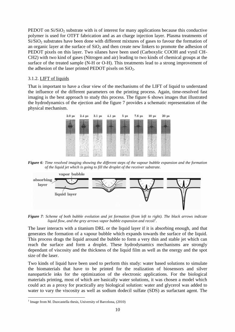
The basic structure of such photopolymers is shown in figure 5. The photocleavable
aryltriazene chromophore is covalently incorporated into the polymer main chain. The
thermodynamic driving force of the photo-triggered fragmentation mechanism is the
formation of elemental nitrogen upon homolytical cleavage of the triazene moiety. The type
of the bridge X has an influence on the absorption range, whereas the length of the spacer unit
Y determines the number of chromophores along the backbone, and therefore the absorption
coefficient. The side chains R at the triazene unit have an influence on the packing behavior of
the polymer chains and allow the introduction of further functional groups in order to tailor
the application properties as e.g. solubility in different solvents and the polarity. The different
triazene polymers developed in the frame of the project fulfilled all the requirements of
absorptivity, cleanliness and solubility.
Figure 5: General chemical structure of aryltriazene photopolymers and as example the derivative DAO-6-Me
that is frequently used as a reference material for LIFT studies. Here, the bridge X is an ether (O), the
spacer Y a C6-alkyl chain and the side-chains R small methyl groups.
d. promotion of adhesion properties
We also investigate the possibility of improving the adhesion of the transferred pixels on the
receiver substrates by means of plasma treatment. An atmospheric plasma treatment tool has
been developed and tested with the different materials and substrates selected. A first set of
treatment has been performed either with air or nitrogen atmosphere. Unfortunately, these
treatments didn’t provide any significant adhesion properties enhancement. Either the initial
adhesion was good enough for the application and doesn’t require any treatment, or the
adhesion was initially poor and no significant improvement was brought by the plasma
treatment.
This negative result had no impact on the project because alternative configurations or
materials have been found. However, the investigated in more details the case of printing
NN
NY
NN
N
R
X
R n
Bridge
Spacer
Side chains
Photocleavable
main chain
Application properties
DAO-6-Me
10
PEDOT on Si/SiO2 substrate with is of interest for many applications because this conductive
polymer is used for OTFT fabrication and as an charge injection layer. Plasma treatments of
Si/SiO2 substrates have been done with different mixtures of gases to favour the formation of
an organic layer at the surface of SiO2 and then create new linkers to promote the adhesion of
PEDOT pixels on this layer. Two silanes have been used (Carboxylic COOH and vynil CH-
CH2) with two kind of gases (Nitrogen and air) leading to two kinds of chemical groups at the
surface of the treated sample (N-H or O-H). This treatments lead to a strong improvement of
the adhesion of the laser printed PEDOT pixels on SiO2.
3.1.2. LIFT of liquids
That is important to have a clear view of the mechanisms of the LIFT of liquid to understand
the influence of the different parameters on the printing process. Again, time-resolved fast
imaging is the best approach to study this process. The figure 6 shows images that illustrated
the hydrodynamics of the ejection and the figure 7 provides a schematic representation of the
physical mechanism.
Figure 6: Time resolved imaging showing the different steps of the vapour bubble expansion and the formation
of the liquid jet which is going to fill the droplet of the receiver substrate.
Figure 7: Scheme of both bubble evolution and jet formation (from left to right). The black arrows indicate
liquid flow, and the grey arrows vapor bubble expansion and recoil1.
The laser interacts with a titanium DRL or the liquid layer if it is absorbing enough, and that
generates the formation of a vapour bubble which expands towards the surface of the liquid.
This process drags the liquid around the bubble to form a very thin and stable jet which can
reach the surface and form a droplet. These hydrodynamics mechanisms are strongly
dependant of viscosity and the thickness of the liquid film as well as the energy and the spot
size of the laser.
Two kinds of liquid have been used to perform this study: water based solutions to simulate
the biomaterials that have to be printed for the realization of biosensors and silver
nanoparticle inks for the optimization of the electronic applications. For the biological
materials printing, most of which are basically water solutions, it was chosen a model which
could act as a proxy for practically any biological solution: water and glycerol was added to
water to vary the viscosity as well as sodium dodecil sulfate (SDS) as surfactant agent. The
1 Image from M. Duocastella thesis, University of Barcelona, (2010)
11
specifications of the inks were the following: 20% wt of silver content, viscosity of 10-30
mPa.s, density of 1.25g/cm3, nanoparticle size in the range of 80-110nm, alcohol based
solvent.
The main conclusions of the study are the following:
For the water glycerol solutions
It is possible to print well-defined droplets in a reproducible way with Ti DRL at all
the considered laser wavelengths (193-1027 nm) and pulse regimes (450 fs-10 ns).
In consequence, there is no strong restriction concerning the selection of laser source
for this application.
The gap between donor and receiving substrate does not constitute any significant
constraint for the process. It is possible to print well-defined droplets for gaps between
20 µm and 2 mm. The possibility of keeping a relatively large gap when working with
liquid films is very relevant from a technological point of view, since this allows
preventing the contact between donor and receiver, which would impede the printing
process.
It is possible to print well-defined droplets of a very wide range of viscosities, at least
from that of pure water, about 1 mPa·s, to that of pure glycerol, about 1000 mPa·s (the
viscosity of the solution was varied through the modification of its glycerol content).
This grants the possibility of printing almost any biological solution. In the case of
very low viscosities (below 3 mPa·s), short gaps (below 50 µm) are required for
printing.
The droplet dimensions achievable through the reported parameters range between
30 µm and several hundreds of microns. Higher resolutions (diameters down to 10
µm) can be attained, but in this case the setting of the process parameters becomes
more critical: small gaps (below 50 µm), small film thicknesses (below 5 µm) and low
laser fluences (100-300 mJ/cm2) are required.
In the case of Ag inks:
It is possible to carry out printing without the use of DRL for any of the considered
laser sources, because these ink formulations absorb well all the analyzed wavelengths
(193-1027 nm). However, Ti DRL allows improving significantly the printing results.
The laser fluence range is broadened (100-300 mJ/cm2) and better uniformity and
reproducibility are achieved.
In a similar way to the water solution printing, the gap between donor and receiving
substrate does neither constitute any significant constraint for the process. However, it
is better to keep the gap below 200 µm in order to completely prevent the presence of
satellite droplets.
The droplet dimensions achievable through the reported parameters range between
20 µm and several hundreds of microns.
Summarizing, LIFT allows printing liquids with few technological constraints. If the process
is carried out through a DRL, practically any of the short-pulsed lasers commonly used in
materials processing applications can be used for such purpose, provided that once the beam
is focused diameters down to some tens of microns and fluences up to a few J/cm2 can be
obtained. Furthermore, from the presented work it is concluded that a really wide range of
rheologies can be successfully printed. In consequence, it is possible to print a great variety of
liquids with practically no engineering of their properties, a certainly time-consuming task in
most conventional printing techniques. This, alongside with its high resolution and its nozzle-
free nature, makes LIFT truly competitive in the printing arena.
12
3.1.3. Printing complex structures
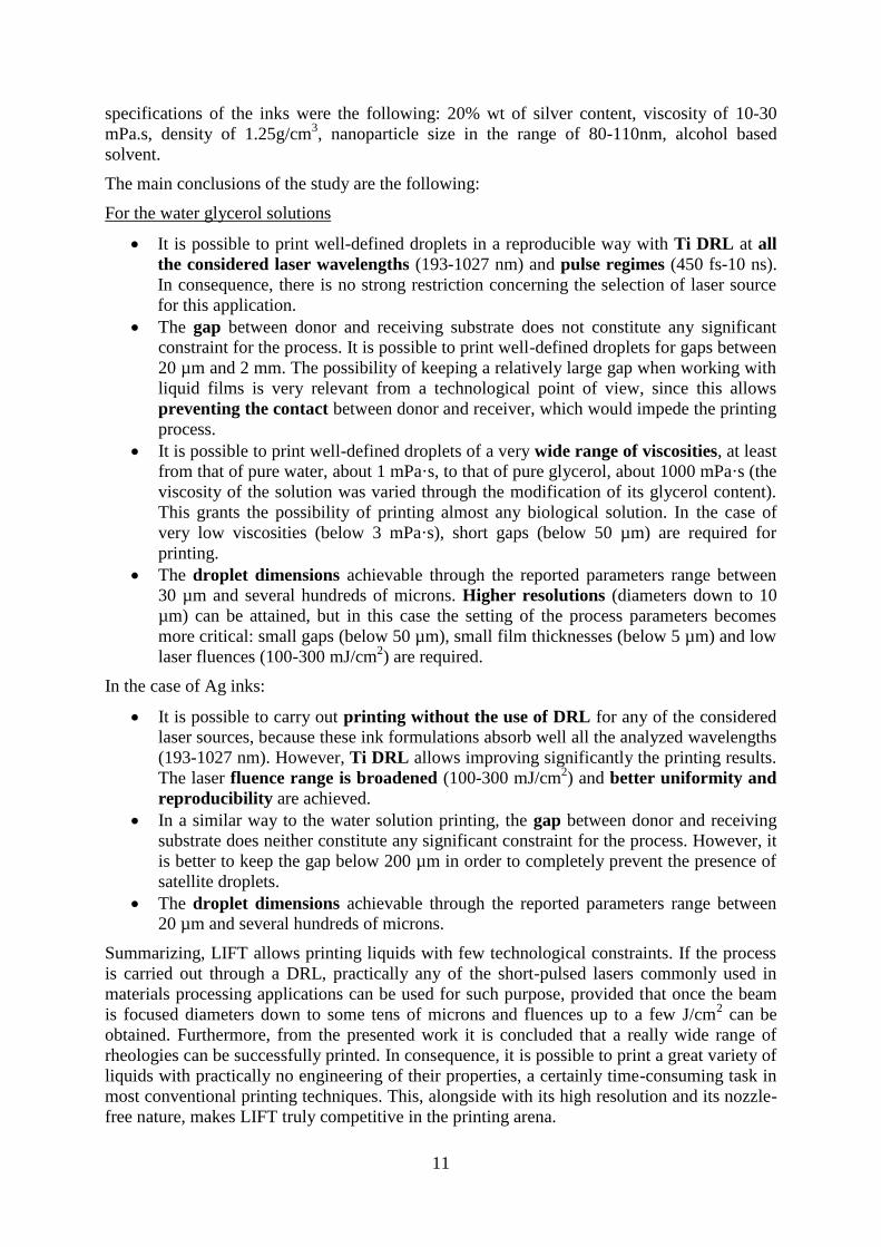
a. Printing of lines from adjacent pixels
For most of the applications of a printing technology, the deposition of continuous lines is
mandatory. These lines have been laser printed by juxtaposition of pixels (solid phase) or
droplets (liquid phase) with a small overlap.
Experiments have been successfully performed with different organic materials (PEDOT,
PQT, CuPc). Figure 8a shows CuPc lines printed with a picosecond laser (@355nm). PEDOT
lines have also been printed with the same methodology and electrical measurements have not
shown any conductivity degradation of the material due to the overlapping. Silver lines have
also been printed in liquid phase by overlapping successive droplets (d < 10 µm). Figures 8b
and 8c show 25m wide silver lines with AFM characterisation of line and channel between
two lines.
(a) (b) (c)
Figure 8: LIFT-printed pixel lines of CuPc (a) and AFM images of 25m width silver lines (b) and of the space
between two lines (c)
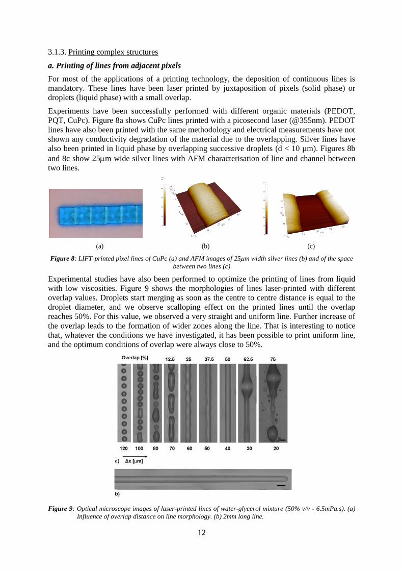
Experimental studies have also been performed to optimize the printing of lines from liquid
with low viscosities. Figure 9 shows the morphologies of lines laser-printed with different
overlap values. Droplets start merging as soon as the centre to centre distance is equal to the
droplet diameter, and we observe scalloping effect on the printed lines until the overlap
reaches 50%. For this value, we observed a very straight and uniform line. Further increase of
the overlap leads to the formation of wider zones along the line. That is interesting to notice
that, whatever the conditions we have investigated, it has been possible to print uniform line,
and the optimum conditions of overlap were always close to 50%.
Figure 9: Optical microscope images of laser-printed lines of water-glycerol mixture (50% v/v - 6.5mPa.s). (a)
Influence of overlap distance on line morphology. (b) 2mm long line.
13
b. Printing multilayer film
The ability of LIFT to print multilayer films is of prime importance for the realization of thin
film transistors (TFT) and of organic light emitting diodes (OLED). Two approaches have
been developed to reach this objective: print successive monolayers and print in a single step
a multilayer film.
Layer by layer printing
The main conclusions we can drawn from the studies performed on this topic are the
following:
Printing layer by layer is required for the realisation of devices with pixels of different
sizes (electrodes on semiconductor).
Laser must be fully absorbed within the donor substrate to avoid any risk of damage of
the previously printed material.
The main advantage of this technique is the possibility of printing pixels in solid phase
on the top of each other without any considerations of solvent compatibility.
Single step printing of multilayer
No supplementary limitation has been observed for the printing of the multilayer films in
comparison with the printing of a single layer. The main advantage of printing multilayer film
in a single step is the guarantee of keeping all the initial properties of the interfaces between
the different layers. The risk of damaging the layers is also strongly reduced. However, this
configuration can only be used when the different pixels of the structure have the same
geometrical features. This approached provided very good results for OLED printing as
described hereafter.
c Conclusions
This task dedicated to the printing of complex structures demonstrated some of the main
advantages of LIFT technology. We can mentioned the deposition of multilayer structures in a
single step, and the printing of conductive pastes with a wide range of viscosities, leading to
the realisation of connexion lines with thickness ranging from 100nm to 30m.
3.2. Application to printing PLEDs
The purpose of this study is to transfer and characterize semiconducting electroluminescent
polymers, in order to print highly resolved RGB pixels with high luminescence efficiency.
The different steps that have been realized to reach this objective are:
• Optimization of material and device configuration.
• Optimization of transfer conditions.
• Characterization of the printed device.
Mainly PFO-based polymers were studied as the electroluminescent material, according to the
proposed concept to generate the green and red emission by blending triplet emitters as
dopants into the PFO matrix. Devices were based on the architecture glass / 140 nm ITO / 60
nm PEDOT:PSS / 40 nm PVK / ~ 50 nm light-emitting polymer (LEP) / Cathode. The LEP
was either plain for blue emission, or PFO doped with 5 wt% Ir(Me-ppy)3 for green emission,
or with 5 wt% btp2Ir(acac) for red emission. Then donor substrates consisted typically of
fused silica / 190 nm TP / 80 nm cathode / PFO (< 10 wt% triplet emitter dye, ~ 50 nm). The
ITO on glass receiver substrates were all coated with 60 nm PEDOT:PSS and 40 nm PVK as
14
a hole transporting layer. The figure 10 shows the structure of both the receiver and donor
substrates, and the figure 11 presents the procedure to transfer of the multilayer film. For all
of these experiments, a ~ 15 m donor-receiver substrate gap has been used with a reduced
environmental pressure of 1 mbar.
(a) (b)
Figure 10: Structures of the receiver (a) and the donor (b) substrates
Figure 11: A scheme of the red-green-blue PFO pixel transfer. The left image shows the transfer of the third,
blue, pixel after the other two colors have already been transferred. The right image shows the
receiver substrate alone with a bias across the three pixels creating electroluminescence.
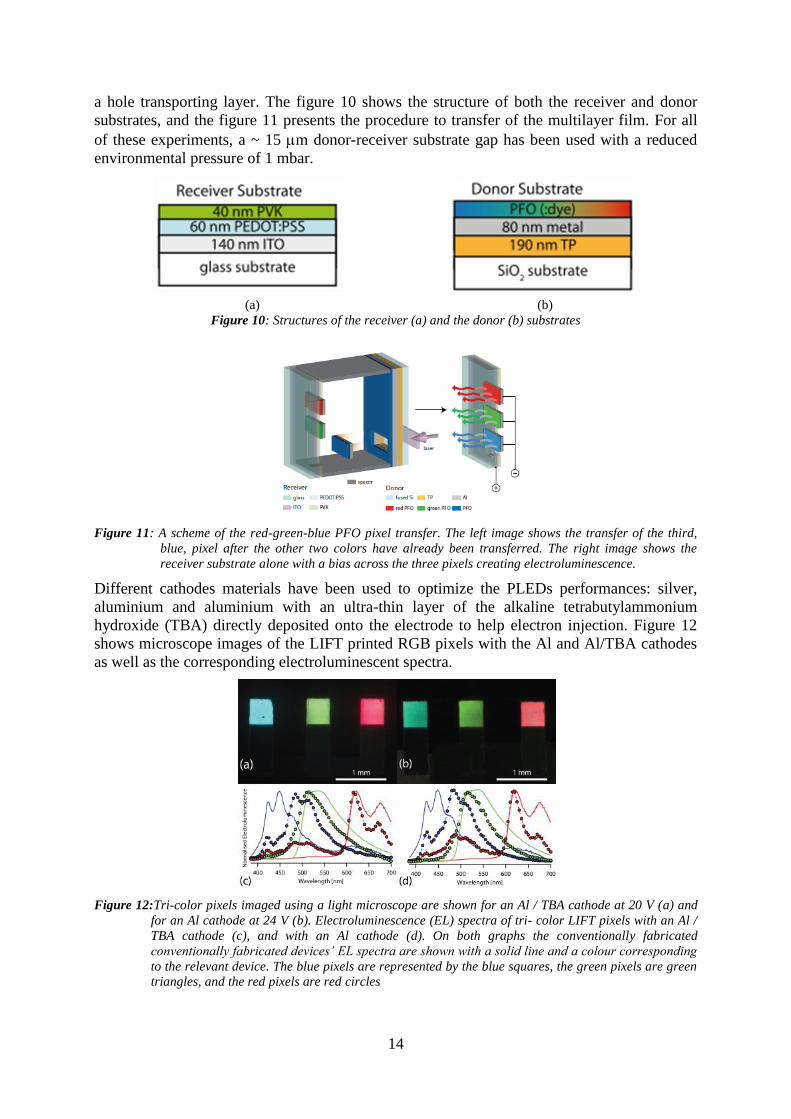
Different cathodes materials have been used to optimize the PLEDs performances: silver,
aluminium and aluminium with an ultra-thin layer of the alkaline tetrabutylammonium
hydroxide (TBA) directly deposited onto the electrode to help electron injection. Figure 12
shows microscope images of the LIFT printed RGB pixels with the Al and Al/TBA cathodes
as well as the corresponding electroluminescent spectra.
Figure 12:Tri-color pixels imaged using a light microscope are shown for an Al / TBA cathode at 20 V (a) and
for an Al cathode at 24 V (b). Electroluminescence (EL) spectra of tri- color LIFT pixels with an Al /
TBA cathode (c), and with an Al cathode (d). On both graphs the conventionally fabricated
conventionally fabricated devices’ EL spectra are shown with a solid line and a colour corresponding
to the relevant device. The blue pixels are represented by the blue squares, the green pixels are green
triangles, and the red pixels are red circles
15
The figure 13 summarizes the performances of the PLED devices for different configurations.
We can observed that luminance as high as 540 cd.m-² for the blue pixel and 232 cd.m
-² and
145 cd.m-² have been obtained for the green and red pixel respectively after the optimization
of the process, the materials and the device configuration.
Table 1: Device performances for various device architectures, at a current density (CD) of ∼ 40-50 mJ cm− 2
.
Blue, Green and Red refer to the LEP layer, whether just plain PFO (Blue), or doped PFO (Red and
Green). The LIFT Al are the LIFTed pixels with plain Al electrodes, LIFT Al / TBA are the LIFTed
pixels with Al / tetrabutylammonium electrodes, the Convent Al are the conventionally fabricated
devices with Al electrodes, and Convent Ca are the conventionally fabricated devices with Ca
electrodes.
So, there is no doubt that laser printing is an appropriate process to realize PLED devices. Its
ability to print multilayer films in a single step process without reduction of the material
performances is a great advantage over other printing technologies.
3.3. Application to printing OTFTs
This part of the project was dedicated to the realization of organic/inorganic TFTs printed by
the Laser Induced Forward Transfer (LIFT) process. The realization of organic/inorganic
TFTs in bottom gate configuration and top gate configuration have been investigated, and a
comparison with the inkjet printing technology was performed.
a. Realization of organic/inorganic TFT in bottom gate configuration
During the project, many different materials have been tested as organic semiconductors
(PBTTT, PQT, P3HT, DS4T, diPhAc-3T, P5, Ν2200) and for the fabrication of the source &
drain electrodes (Au, Ag or Pt) which have been either evaporated or lithographed. We
investigated p or n-channel TFTs with combinations of organic or inorganic materials,
respectively. All the results will not be presented but this report focused on the most
significant ones to illustrate the plus and cons of the laser printing process for this specific
application.
First, we printed PQT-12 based transistors. The receiver substrate was silicon (Si) covered by
a 300 nm thick silicon dioxide (SiO2) layer, and these materials play also the role of gate and
dielectric of the transistors, respectively. Pixels of 80 nm thick PQT-12 were printed on this
receiver substrate, then, the OTFTs were completed by thermally evaporated 50 nm thick gold
lines through a mask as source-drain electrodes in a top contact (TC) configuration with
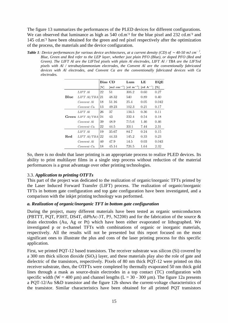
specific width (W = 400 µm) and channel lengths (L = 30 - 300 µm). The figure 12a presents
a PQT-12/Au S&D transistor and the figure 12b shows the current-voltage characteristics of
the transistor. Similar characteristics have been obtained for all printed PQT transistors
16
printed in the optimized conditions. A mobility of 2.4 × 10⁻² cm2.V-1.s-1 has been measured
with a threshold voltage VT = - 9 V and IOn/IOff ratio of 3 103.
(a) (b)
Figure 12: Optical microscope image (a) and output characteristics (b) of PQT-12 based transistor with 30nm
thick gold source/drain electrodes (W = 300 µm, L = 50 µm)
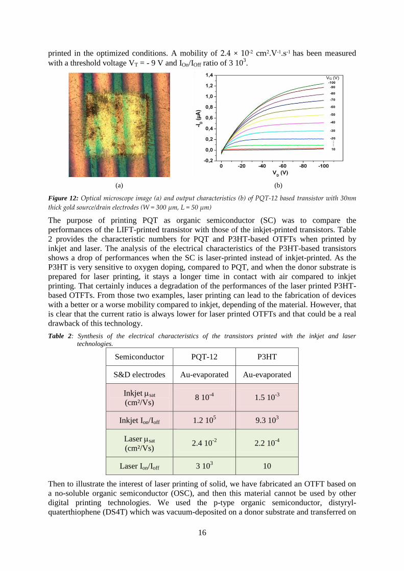
The purpose of printing PQT as organic semiconductor (SC) was to compare the
performances of the LIFT-printed transistor with those of the inkjet-printed transistors. Table
2 provides the characteristic numbers for PQT and P3HT-based OTFTs when printed by
inkjet and laser. The analysis of the electrical characteristics of the P3HT-based transistors
shows a drop of performances when the SC is laser-printed instead of inkjet-printed. As the
P3HT is very sensitive to oxygen doping, compared to PQT, and when the donor substrate is
prepared for laser printing, it stays a longer time in contact with air compared to inkjet
printing. That certainly induces a degradation of the performances of the laser printed P3HT-
based OTFTs. From those two examples, laser printing can lead to the fabrication of devices
with a better or a worse mobility compared to inkjet, depending of the material. However, that
is clear that the current ratio is always lower for laser printed OTFTs and that could be a real
drawback of this technology.
Table 2: Synthesis of the electrical characteristics of the transistors printed with the inkjet and laser
technologies.
Semiconductor PQT-12 P3HT
S&D electrodes Au-evaporated Au-evaporated
Inkjet sat
(cm²/Vs) 8 10
-4 1.5 10
-3
Inkjet Ion/Ioff 1.2 105 9.3 10
3
Laser sat
(cm²/Vs) 2.4 10
-2 2.2 10
-4
Laser Ion/Ioff 3 103 10
Then to illustrate the interest of laser printing of solid, we have fabricated an OTFT based on
a no-soluble organic semiconductor (OSC), and then this material cannot be used by other
digital printing technologies. We used the p-type organic semiconductor, distyryl-
quaterthiophene (DS4T) which was vacuum-deposited on a donor substrate and transferred on
17
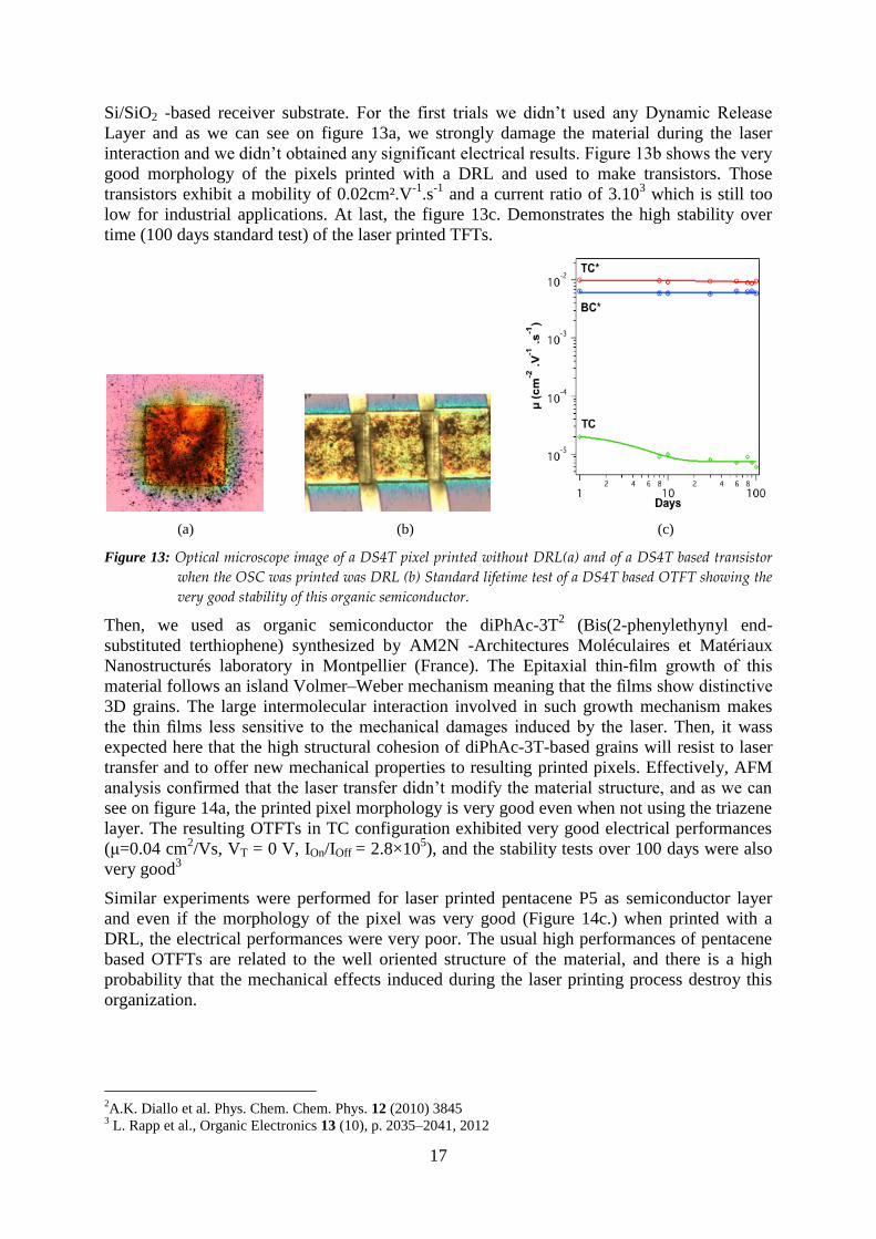
Si/SiO2 -based receiver substrate. For the first trials we didn’t used any Dynamic Release
Layer and as we can see on figure 13a, we strongly damage the material during the laser
interaction and we didn’t obtained any significant electrical results. Figure 13b shows the very
good morphology of the pixels printed with a DRL and used to make transistors. Those
transistors exhibit a mobility of 0.02cm².V-1
.s-1
and a current ratio of 3.103 which is still too
low for industrial applications. At last, the figure 13c. Demonstrates the high stability over
time (100 days standard test) of the laser printed TFTs.
(a) (b) (c)
Figure 13: Optical microscope image of a DS4T pixel printed without DRL(a) and of a DS4T based transistor
when the OSC was printed was DRL (b) Standard lifetime test of a DS4T based OTFT showing the
very good stability of this organic semiconductor.
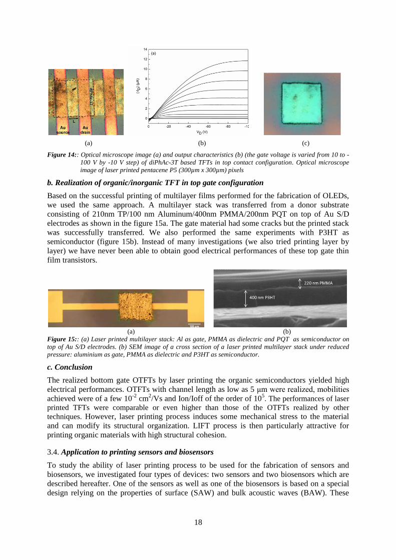
Then, we used as organic semiconductor the diPhAc-3T2 (Bis(2-phenylethynyl end-
substituted terthiophene) synthesized by AM2N -Architectures Moléculaires et Matériaux
Nanostructurés laboratory in Montpellier (France). The Epitaxial thin-film growth of this
material follows an island Volmer–Weber mechanism meaning that the films show distinctive
3D grains. The large intermolecular interaction involved in such growth mechanism makes
the thin films less sensitive to the mechanical damages induced by the laser. Then, it wass
expected here that the high structural cohesion of diPhAc-3T-based grains will resist to laser
transfer and to offer new mechanical properties to resulting printed pixels. Effectively, AFM
analysis confirmed that the laser transfer didn’t modify the material structure, and as we can
see on figure 14a, the printed pixel morphology is very good even when not using the triazene
layer. The resulting OTFTs in TC configuration exhibited very good electrical performances
(μ=0.04 cm2/Vs, VT = 0 V, IOn/IOff = 2.8×10
5), and the stability tests over 100 days were also
very good3
Similar experiments were performed for laser printed pentacene P5 as semiconductor layer
and even if the morphology of the pixel was very good (Figure 14c.) when printed with a
DRL, the electrical performances were very poor. The usual high performances of pentacene
based OTFTs are related to the well oriented structure of the material, and there is a high
probability that the mechanical effects induced during the laser printing process destroy this
organization.
2A.K. Diallo et al. Phys. Chem. Chem. Phys. 12 (2010) 3845
3 L. Rapp et al., Organic Electronics 13 (10), p. 2035–2041, 2012
18
(a) (b) (c)
Figure 14:: Optical microscope image (a) and output characteristics (b) (the gate voltage is varied from 10 to -
100 V by -10 V step) of diPhAc-3T based TFTs in top contact configuration. Optical microscope
image of laser printed pentacene P5 (300µm x 300µm) pixels
b. Realization of organic/inorganic TFT in top gate configuration
Based on the successful printing of multilayer films performed for the fabrication of OLEDs,
we used the same approach. A multilayer stack was transferred from a donor substrate
consisting of 210nm TP/100 nm Aluminum/400nm PMMA/200nm PQT on top of Au S/D
electrodes as shown in the figure 15a. The gate material had some cracks but the printed stack
was successfully transferred. We also performed the same experiments with P3HT as
semiconductor (figure 15b). Instead of many investigations (we also tried printing layer by
layer) we have never been able to obtain good electrical performances of these top gate thin
film transistors.
(a) (b)
Figure 15:: (a) Laser printed multilayer stack: Al as gate, PMMA as dielectric and PQT as semiconductor on
top of Au S/D electrodes. (b) SEM image of a cross section of a laser printed multilayer stack under reduced
pressure: aluminium as gate, PMMA as dielectric and P3HT as semiconductor.
c. Conclusion
The realized bottom gate OTFTs by laser printing the organic semiconductors yielded high
electrical performances. OTFTs with channel length as low as 5 μm were realized, mobilities
achieved were of a few 10-2
cm2/Vs and Ion/Ioff of the order of 10
5. The performances of laser
printed TFTs were comparable or even higher than those of the OTFTs realized by other
techniques. However, laser printing process induces some mechanical stress to the material
and can modify its structural organization. LIFT process is then particularly attractive for
printing organic materials with high structural cohesion.
3.4. Application to printing sensors and biosensors
To study the ability of laser printing process to be used for the fabrication of sensors and
biosensors, we investigated four types of devices: two sensors and two biosensors which are
described hereafter. One of the sensors as well as one of the biosensors is based on a special
design relying on the properties of surface (SAW) and bulk acoustic waves (BAW). These
19
systems will not be described here but a complete description of these devices have been
published4,5
3.4.1. Chemical sensors for organic compounds based on chemical-selective polymeric
materials
The purpose of this task was to fabricate a sensor array for monitoring volatile organic
compounds (VOCs) by combining the sensitivity of specially designed SAW/BAW devices
with the selectivity of special polymers and their combination in one device.
The different steps to perform this study have been the following:
- Fabrication of SAW Sensors and SAW sensor arrays.
- Preparation of different donor substrates (PEI, PIB, PECH, PScMA-me, HPMC) by
MAPLE (laser deposition process) for the transfer of polymer pixels.
- PEI, PIB, PECH, PScMA-me, HPMC pixels from different donor substrates were
transferred on individual sensors and sensor arrays.
- Fabrication of a prototype system for the characterization of the 6 elements (5 sensors
plus a reference) arrays.
- Sensitivity evaluation of the transferred pixels (PEI, PIB, PECH) for dimethyl
methylphosphonate (DMMP), dichloromethane (DCM), and ethylacetate (EtOAc).
Linear responses to the concentration of the chemical compounds have been obtained
for the three polymers, and a detection limit of 0.15 has been reached for the detection
of DMMP by PEHC polymer.
- Sensitivity evaluation of the transferred pixels (PEI, PIB, PECH, PScMA-me, HPMC)
for toluene (Tol), water (H2O), and dichloropentane (DCP).
- Principal Component Analysis (PCA) of the responses of the array composed of 3 and 5
SAW sensors.
- Evaluation of the capability of the arrays to discriminate different analytes.
The main results of this study are summarized hereafter
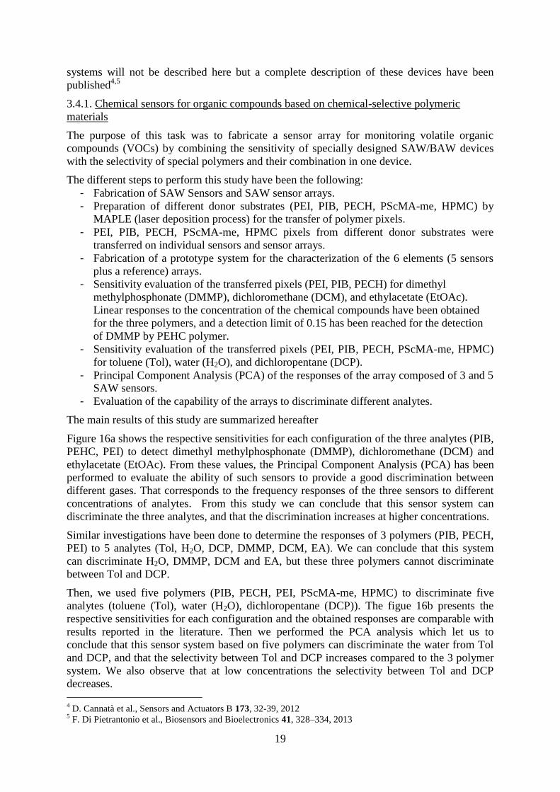
Figure 16a shows the respective sensitivities for each configuration of the three analytes (PIB,
PEHC, PEI) to detect dimethyl methylphosphonate (DMMP), dichloromethane (DCM) and
ethylacetate (EtOAc). From these values, the Principal Component Analysis (PCA) has been
performed to evaluate the ability of such sensors to provide a good discrimination between
different gases. That corresponds to the frequency responses of the three sensors to different
concentrations of analytes. From this study we can conclude that this sensor system can
discriminate the three analytes, and that the discrimination increases at higher concentrations.
Similar investigations have been done to determine the responses of 3 polymers (PIB, PECH,
PEI) to 5 analytes (Tol, H2O, DCP, DMMP, DCM, EA). We can conclude that this system
can discriminate H2O, DMMP, DCM and EA, but these three polymers cannot discriminate
between Tol and DCP.
Then, we used five polymers (PIB, PECH, PEI, PScMA-me, HPMC) to discriminate five
analytes (toluene (Tol), water (H2O), dichloropentane (DCP)). The figue 16b presents the
respective sensitivities for each configuration and the obtained responses are comparable with
results reported in the literature. Then we performed the PCA analysis which let us to
conclude that this sensor system based on five polymers can discriminate the water from Tol
and DCP, and that the selectivity between Tol and DCP increases compared to the 3 polymer
system. We also observe that at low concentrations the selectivity between Tol and DCP
decreases.
4 D. Cannatà et al., Sensors and Actuators B 173, 32-39, 2012
5 F. Di Pietrantonio et al., Biosensors and Bioelectronics 41, 328–334, 2013
20
(a) (b)
Figure 16: Sensitivity of SAW sensors coated with PIB, PECH, PEI to DMMP, DCM, EtOAc (a) and Sensitivity
of 5 polymers (PIB, PECH, PEI, PS, HPMC) coated sensor matrices to Toluene, H2O and DCP (b).
3.4.2. Biosensors based on proteins
The purpose of this task was to realize biosensors based on a SAW and combining the
sensitivity of biomolecules. The different steps performed in this study have been the
following:
- Fabrication of SAW devices.
- Purification and functionality test of three proteins: wild type bovine Odorant-Binding
Protein (wtbOBO), double mutant bOBP (dmbOBP) and wild type pig OBP (wtpOBP).
- Transfer by LIFT on SAW devices of the three proteins.
- Optimization of the LIFT depositions of the proteins in order to obtain uniform
coverage of the SAW device active area without any drying issues.
- Fabrication of a prototype system for the characterization of the arrays consisting of 3
sensors (each sensor coated with a different protein) and reference devices.
- Sensitivity evaluation of SAW biosensor arrays upon exposure to R-(–)-1-octen-3-ol
(octenol) and R-(–)-carvone (carvone).
- Principal Component Analysis (PCA) of the responses of the arrays.
- Evaluation of the capability of the arrays to discriminate different analytes.
The optimization of the laser printing step has shown that liquid printing is favorable to the
one from solid donors. In spite that high viscosities allow a better printing control, low
glycerol contents are the best choice for printing the SAW devices with the selected protein
solutions (figure 17). In this case it is always possible to find a window of process parameters
allowing the accurate and uniform coverage of the entire active area without any drying issues
(coffee-ring effect). In these conditions several arrays of SAW devices have been printed with
the three different protein solutions and submitted to characterization and functionality tests.
The SAW biosensor arrays are composed of three SAW devices coated by LIFT method with
the three chosen proteins: wtbOBP, dmbOBP and wtpOBP. An uncoated device is used to
compensate the variations of the environmental parameters. The biosensor system was tested
in N2 atmosphere upon exposure to vapours of octenol (also called mushroom alcohol, is an
enantiomer produced by several plants and fungi) and carvone (an enantiomer that smell like
spearmint).
21
Figure 17: Optical microscopy images of SAW devices printed with a 50% glycerol solution (a) and a 20%
glycerol solution (b) of wtOBP
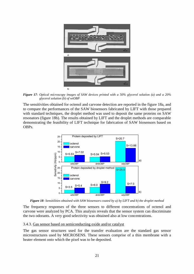
The sensitivities obtained for octenol and carvone detection are reported in the figure 18a, and
to compare the performances of the SAW biosensors fabricated by LIFT with those prepared
with standard techniques, the droplet method was used to deposit the same proteins on SAW
resonators (figure 18b). The results obtained by LIFT and the droplet methods are comparable
demonstrating the feasibility of LIFT technique for fabrication of SAW biosensors based on
OBPs.
Figure 18: Sensitilities obtained with SAW biosensors coated by a) by LIFT and b) the droplet method
The frequency responses of the three sensors to different concentrations of octenol and
carvone were analyzed by PCA. This analysis reveals that the sensor system can discriminate
the two odorants. A very good selectivity was obtained also at low concentrations.
3.4.3. Gas sensor based on semiconducting oxide and/or catalyst
The gas sensor structures used for the transfer evaluation are the standard gas sensor
microstructures used by MICROSENS. These sensors comprise of a thin membrane with a
heater element onto which the pixel was to be deposited.
22
Different approaches have been suggested and tested to prepare the donor substrates used to
laser print the SnO2 film. The best results have been obtained with a precursor of
SnCl2(acac)2. We also observed that the absence of the DRL does not influence the quality of
the transfer. Since the SnCl2(acac)2 based pixels show the most promise for the sensor
fabrication, the evaluation of the sensor characteristics was performed using these types of
pixels. Furthermore, this precursor was used to evaluate the effect of Pd doping of the sensor
pixel.
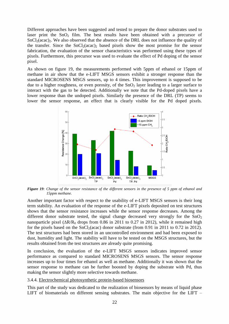
As shown on figure 19, the measurements performed with 5ppm of ethanol or 15ppm of
methane in air show that the e-LIFT MSGS sensors exhibit a stronger response than the
standard MICROSENS MSGS sensors, up to 4 times. This improvement is supposed to be
due to a higher roughness, or even porosity, of the SnO2 layer leading to a larger surface to
interact with the gas to be detected. Additionally we note that the Pd-doped pixels have a
lower response than the undoped pixels. Similarly the presence of the DRL (TP) seems to
lower the sensor response, an effect that is clearly visible for the Pd doped pixels.
Figure 19: Change of the sensor resistance of the different sensors in the presence of 5 ppm of ethanol and
15ppm methane.
Another important factor with respect to the usability of e-LIFT MSGS sensors is their long
term stability. An evaluation of the response of the e-LIFT pixels deposited on test structures
shows that the sensor resistance increases while the sensor response decreases. Among the
different donor substrate tested, the signal change decreased very strongly for the SnO2
nanoparticle pixel (R/R0 drops from 0.86 in 2011 to 0.27 in 2012), while it remained high
for the pixels based on the SnCl2(acac) donor substrate (from 0.91 in 2011 to 0.72 in 2012).
The test structures had been stored in an uncontrolled environment and had been exposed to
dust, humidity and light. The stability will have to be tested on the MSGS structures, but the
results obtained from the test structures are already quite promising.
In conclusion, the evaluation of the e-LIFT MSGS sensors indicates improved sensor
performance as compared to standard MICROSENS MSGS sensors. The sensor response
increases up to four times for ethanol as well as methane. Additionally it was shown that the
sensor response to methane can be further boosted by doping the substrate with Pd, thus
making the sensor slightly more selective towards methane.
3.4.4. Electrochemical photosynthetic protein-based biosensors
This part of the study was dedicated to the realization of biosensors by means of liquid phase
LIFT of biomaterials on different sensing substrates. The main objective for the LIFT –
23
assisted realization of biosensors task is the development of advanced electrochemical devices
for pollutant monitoring. The specific target application is the high sensitivity detection of
pesticides and herbicides in water and agro-food products.
The principle of the biosensor is based on the electrochemical detection using photosynthetic
proteins based on the properties of the thylakoid membrane. The proteins are printed on a
screen printed gold electrodes (Au SPE). This electrode is placed in water and illuminated by
the light from a pulsed LED. Under illumination the proteins generate a electrons which are
collected by the SPE and the intensity of the current represents the response of the sensor.
When herbicides or pesticides are present in the water, they attach to the proteins and reduce
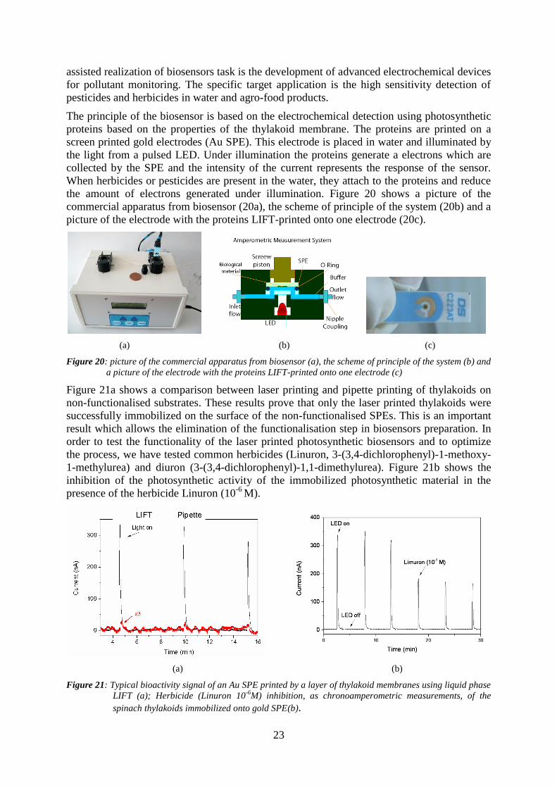
the amount of electrons generated under illumination. Figure 20 shows a picture of the
commercial apparatus from biosensor (20a), the scheme of principle of the system (20b) and a
picture of the electrode with the proteins LIFT-printed onto one electrode (20c).
(a) (b) (c)
Figure 20: picture of the commercial apparatus from biosensor (a), the scheme of principle of the system (b) and
a picture of the electrode with the proteins LIFT-printed onto one electrode (c)
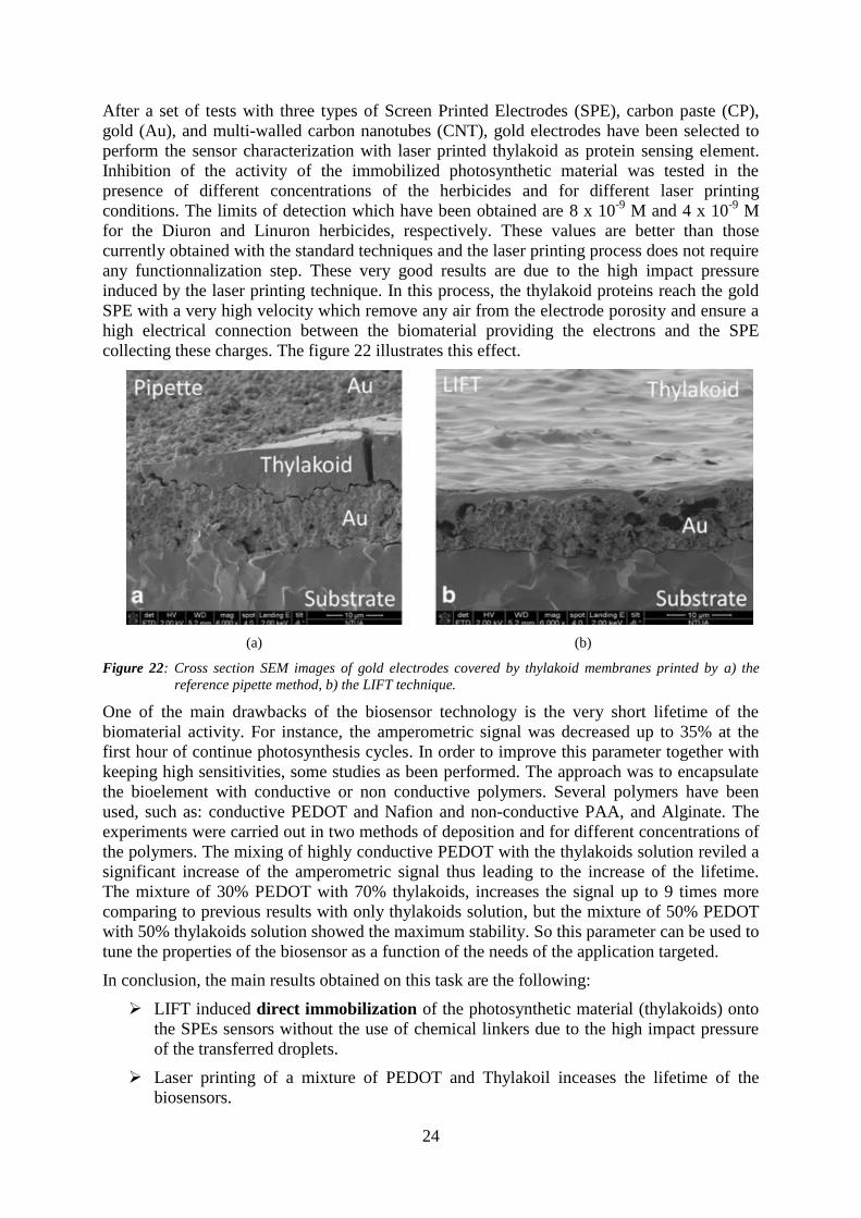
Figure 21a shows a comparison between laser printing and pipette printing of thylakoids on
non-functionalised substrates. These results prove that only the laser printed thylakoids were
successfully immobilized on the surface of the non-functionalised SPEs. This is an important
result which allows the elimination of the functionalisation step in biosensors preparation. In
order to test the functionality of the laser printed photosynthetic biosensors and to optimize
the process, we have tested common herbicides (Linuron, 3-(3,4-dichlorophenyl)-1-methoxy-
1-methylurea) and diuron (3-(3,4-dichlorophenyl)-1,1-dimethylurea). Figure 21b shows the
inhibition of the photosynthetic activity of the immobilized photosynthetic material in the
presence of the herbicide Linuron (10-6
M).
(a) (b)
Figure 21: Typical bioactivity signal of an Au SPE printed by a layer of thylakoid membranes using liquid phase
LIFT (a); Herbicide (Linuron 10-6
M) inhibition, as chronoamperometric measurements, of the
spinach thylakoids immobilized onto gold SPE(b).
24
After a set of tests with three types of Screen Printed Electrodes (SPE), carbon paste (CP),
gold (Au), and multi-walled carbon nanotubes (CNT), gold electrodes have been selected to
perform the sensor characterization with laser printed thylakoid as protein sensing element.
Inhibition of the activity of the immobilized photosynthetic material was tested in the
presence of different concentrations of the herbicides and for different laser printing
conditions. The limits of detection which have been obtained are 8 x 10⁻⁹
M and 4 x 10⁻⁹
M
for the Diuron and Linuron herbicides, respectively. These values are better than those
currently obtained with the standard techniques and the laser printing process does not require
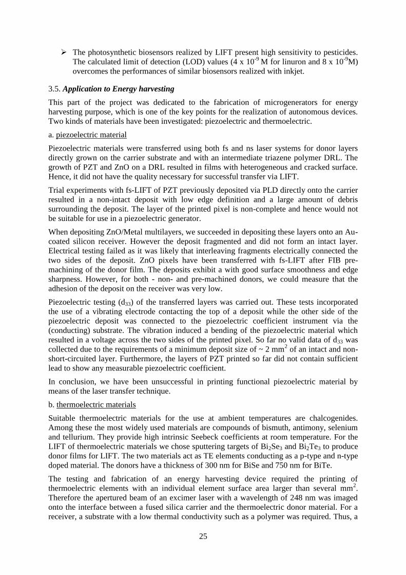
any functionnalization step. These very good results are due to the high impact pressure
induced by the laser printing technique. In this process, the thylakoid proteins reach the gold
SPE with a very high velocity which remove any air from the electrode porosity and ensure a
high electrical connection between the biomaterial providing the electrons and the SPE
collecting these charges. The figure 22 illustrates this effect.
(a) (b)
Figure 22: Cross section SEM images of gold electrodes covered by thylakoid membranes printed by a) the
reference pipette method, b) the LIFT technique.
One of the main drawbacks of the biosensor technology is the very short lifetime of the
biomaterial activity. For instance, the amperometric signal was decreased up to 35% at the
first hour of continue photosynthesis cycles. In order to improve this parameter together with
keeping high sensitivities, some studies as been performed. The approach was to encapsulate
the bioelement with conductive or non conductive polymers. Several polymers have been
used, such as: conductive PEDOT and Nafion and non-conductive PAA, and Alginate. The
experiments were carried out in two methods of deposition and for different concentrations of
the polymers. The mixing of highly conductive PEDOT with the thylakoids solution reviled a
significant increase of the amperometric signal thus leading to the increase of the lifetime.
The mixture of 30% PEDOT with 70% thylakoids, increases the signal up to 9 times more
comparing to previous results with only thylakoids solution, but the mixture of 50% PEDOT
with 50% thylakoids solution showed the maximum stability. So this parameter can be used to
tune the properties of the biosensor as a function of the needs of the application targeted.
In conclusion, the main results obtained on this task are the following:
LIFT induced direct immobilization of the photosynthetic material (thylakoids) onto
the SPEs sensors without the use of chemical linkers due to the high impact pressure
of the transferred droplets.
Laser printing of a mixture of PEDOT and Thylakoil inceases the lifetime of the
biosensors.
25
The photosynthetic biosensors realized by LIFT present high sensitivity to pesticides.
The calculated limit of detection (LOD) values (4 x 10⁻⁹
M for linuron and 8 x 10⁻⁹
M)
overcomes the performances of similar biosensors realized with inkjet.
3.5. Application to Energy harvesting
This part of the project was dedicated to the fabrication of microgenerators for energy
harvesting purpose, which is one of the key points for the realization of autonomous devices.
Two kinds of materials have been investigated: piezoelectric and thermoelectric.
a. piezoelectric material
Piezoelectric materials were transferred using both fs and ns laser systems for donor layers
directly grown on the carrier substrate and with an intermediate triazene polymer DRL. The
growth of PZT and ZnO on a DRL resulted in films with heterogeneous and cracked surface.
Hence, it did not have the quality necessary for successful transfer via LIFT.
Trial experiments with fs-LIFT of PZT previously deposited via PLD directly onto the carrier
resulted in a non-intact deposit with low edge definition and a large amount of debris
surrounding the deposit. The layer of the printed pixel is non-complete and hence would not
be suitable for use in a piezoelectric generator.
When depositing ZnO/Metal multilayers, we succeeded in depositing these layers onto an Au-
coated silicon receiver. However the deposit fragmented and did not form an intact layer.
Electrical testing failed as it was likely that interleaving fragments electrically connected the
two sides of the deposit. ZnO pixels have been transferred with fs-LIFT after FIB pre-
machining of the donor film. The deposits exhibit a with good surface smoothness and edge
sharpness. However, for both - non- and pre-machined donors, we could measure that the
adhesion of the deposit on the receiver was very low.
Piezoelectric testing (d33) of the transferred layers was carried out. These tests incorporated
the use of a vibrating electrode contacting the top of a deposit while the other side of the
piezoelectric deposit was connected to the piezoelectric coefficient instrument via the
(conducting) substrate. The vibration induced a bending of the piezoelectric material which
resulted in a voltage across the two sides of the printed pixel. So far no valid data of d33 was
collected due to the requirements of a minimum deposit size of ~ 2 mm2 of an intact and non-
short-circuited layer. Furthermore, the layers of PZT printed so far did not contain sufficient
lead to show any measurable piezoelectric coefficient.
In conclusion, we have been unsuccessful in printing functional piezoelectric material by
means of the laser transfer technique.
b. thermoelectric materials
Suitable thermoelectric materials for the use at ambient temperatures are chalcogenides.
Among these the most widely used materials are compounds of bismuth, antimony, selenium
and tellurium. They provide high intrinsic Seebeck coefficients at room temperature. For the
LIFT of thermoelectric materials we chose sputtering targets of Bi2Se3 and Bi2Te3 to produce
donor films for LIFT. The two materials act as TE elements conducting as a p-type and n-type
doped material. The donors have a thickness of 300 nm for BiSe and 750 nm for BiTe.
The testing and fabrication of an energy harvesting device required the printing of
thermoelectric elements with an individual element surface area larger than several mm2.
Therefore the apertured beam of an excimer laser with a wavelength of 248 nm was imaged
onto the interface between a fused silica carrier and the thermoelectric donor material. For a
receiver, a substrate with a low thermal conductivity such as a polymer was required. Thus, a
26
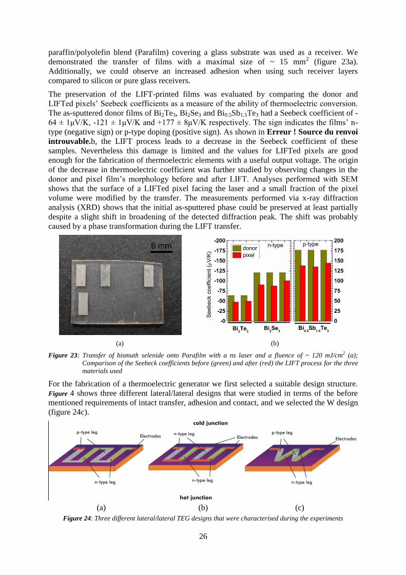
paraffin/polyolefin blend (Parafilm) covering a glass substrate was used as a receiver. We
demonstrated the transfer of films with a maximal size of ~ 15 mm2 (figure 23a).
Additionally, we could observe an increased adhesion when using such receiver layers
compared to silicon or pure glass receivers.
The preservation of the LIFT-printed films was evaluated by comparing the donor and
LIFTed pixels’ Seebeck coefficients as a measure of the ability of thermoelectric conversion.
The as-sputtered donor films of Bi2Te3, Bi2Se3 and Bi0.5Sb1.5Te3 had a Seebeck coefficient of -
64 ± 1μV/K, -121 ± 1μV/K and +177 ± 8μV/K respectively. The sign indicates the films’ n-
type (negative sign) or p-type doping (positive sign). As shown in Erreur ! Source du renvoi
introuvable.b, the LIFT process leads to a decrease in the Seebeck coefficient of these
samples. Nevertheless this damage is limited and the values for LIFTed pixels are good
enough for the fabrication of thermoelectric elements with a useful output voltage. The origin
of the decrease in thermoelectric coefficient was further studied by observing changes in the
donor and pixel film’s morphology before and after LIFT. Analyses performed with SEM
shows that the surface of a LIFTed pixel facing the laser and a small fraction of the pixel
volume were modified by the transfer. The measurements performed via x-ray diffraction
analysis (XRD) shows that the initial as-sputtered phase could be preserved at least partially
despite a slight shift in broadening of the detected diffraction peak. The shift was probably
caused by a phase transformation during the LIFT transfer.
(a) (b)
Figure 23: Transfer of bismuth selenide onto Parafilm with a ns laser and a fluence of ~ 120 mJ/cm2 (a);
Comparison of the Seebeck coefficients before (green) and after (red) the LIFT process for the three
materials used
For the fabrication of a thermoelectric generator we first selected a suitable design structure.
Figure 4 shows three different lateral/lateral designs that were studied in terms of the before
mentioned requirements of intact transfer, adhesion and contact, and we selected the W design
(figure 24c).
(a) (b) (c)
Figure 24: Three different lateral/lateral TEG designs that were characterised during the experiments
27
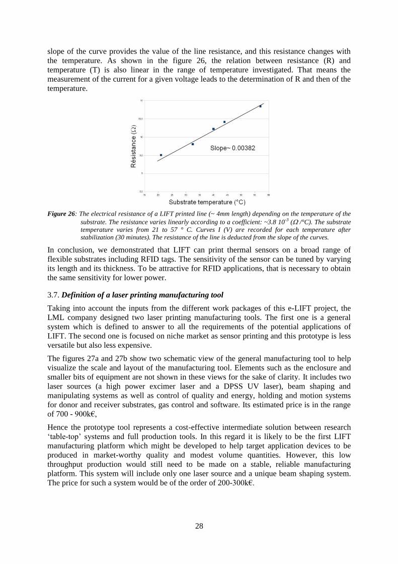
The characterization of LIFT-printed thermoelectric microgenerators was performed was
performed varying the number of legs. Seebeck coefficient was lower than expected from the
previous Seebeck measurements of single LIFTed pixels. However the highest output
voltage/thermocouple for a temperature gradient of ~100K was ~7mV. Hence, the number of
9-10 thermocouples of our devices provides an output voltage sufficiently high to drive
commercially available electronic integrated circuits designated to operate in conjunction with
such energy harvesting generators.
In conclusion, we demonstrated the possibility of laser printing thermoelectric
microgenerators for energy harvesting, and this process outdoes conventional techniques in
terms of flexibility whilst maintaining accuracy and micron resolution of the created
structures. With careful preparation, devices with sophisticated design could be realised as the
receiver coating is a mechanically flexible polymer film. Unfortunately, LIFT is based on a
mechanical effect to transfer material and it is not well-adapted to the printing of thick and
brittle materials required for energy harvesting. Moreover, this process induces some
modifications of the printed material, mainly of thermal and chemical origin, which lowers
the performances of the microgenerators.
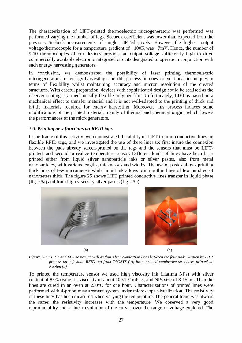
3.6. Printing new functions on RFID tags
In the frame of this activity, we demonstrated the ability of LIFT to print conductive lines on
flexible RFID tags, and we investigated the use of these lines to: first insure the connexion
between the pads already screen-printed on the tags and the sensors that must be LIFT-
printed, and second to realize temperature sensor. Different kinds of lines have been laser
printed either from liquid silver nanoparticle inks or silver pastes, also from metal
nanoparticles, with various lengths, thicknesses and widths. The use of pastes allows printing
thick lines of few micrometers while liquid ink allows printing thin lines of few hundred of
nanometers thick. The figure 25 shows LIFT printed conductive lines transfer in liquid phase
(fig. 25a) and from high viscosity silver pastes (fig. 25b)
(a) (b)
Figure 25: e-LIFT and LP3 names, as well as thin silver connection lines between the four pads, written by LIFT
process on a flexible RFID tag from TAGSYS (a); laser printed conductive structures printed on
Kapton (b)
To printed the temperature sensor we used high viscosity ink (Harima NPs) with silver
content of 85% (weight), viscosity of about 100.103 mPa.s, and NPs size of 8-15nm. Then the
lines are cured in an oven at 230°C for one hour. Characterizations of printed lines were
performed with 4-probe measurement system under microscope visualization. The resistivity
of these lines has been measured when varying the temperature. The general trend was always
the same: the resistivity increases with the temperature. We observed a very good
reproducibility and a linear evolution of the curves over the range of voltage explored. The
28
slope of the curve provides the value of the line resistance, and this resistance changes with
the temperature. As shown in the figure 26, the relation between resistance (R) and
temperature (T) is also linear in the range of temperature investigated. That means the
measurement of the current for a given voltage leads to the determination of R and then of the
temperature.
Figure 26: The electrical resistance of a LIFT printed line (~ 4mm length) depending on the temperature of the
substrate. The resistance varies linearly according to a coefficient: ~3.8 10-3
( /°C). The substrate
temperature varies from 21 to 57 ° C. Curves I (V) are recorded for each temperature after
stabilization (30 minutes). The resistance of the line is deducted from the slope of the curves.
In conclusion, we demonstrated that LIFT can print thermal sensors on a broad range of
flexible substrates including RFID tags. The sensitivity of the sensor can be tuned by varying
its length and its thickness. To be attractive for RFID applications, that is necessary to obtain
the same sensitivity for lower power.
3.7. Definition of a laser printing manufacturing tool
Taking into account the inputs from the different work packages of this e-LIFT project, the
LML company designed two laser printing manufacturing tools. The first one is a general
system which is defined to answer to all the requirements of the potential applications of
LIFT. The second one is focused on niche market as sensor printing and this prototype is less
versatile but also less expensive.
The figures 27a and 27b show two schematic view of the general manufacturing tool to help
visualize the scale and layout of the manufacturing tool. Elements such as the enclosure and
smaller bits of equipment are not shown in these views for the sake of clarity. It includes two
laser sources (a high power excimer laser and a DPSS UV laser), beam shaping and
manipulating systems as well as control of quality and energy, holding and motion systems
for donor and receiver substrates, gas control and software. Its estimated price is in the range
of 700 - 900k€,
Hence the prototype tool represents a cost-effective intermediate solution between research
‘table-top’ systems and full production tools. In this regard it is likely to be the first LIFT
manufacturing platform which might be developed to help target application devices to be
produced in market-worthy quality and modest volume quantities. However, this low
throughput production would still need to be made on a stable, reliable manufacturing
platform. This system will include only one laser source and a unique beam shaping system.
The price for such a system would be of the order of 200-300k€.
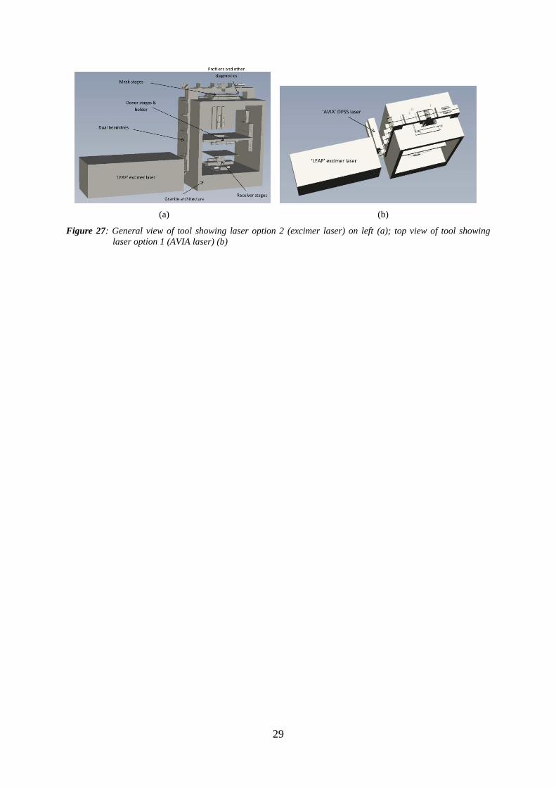
29
(a) (b)
Figure 27: General view of tool showing laser option 2 (excimer laser) on left (a); top view of tool showing
laser option 1 (AVIA laser) (b)
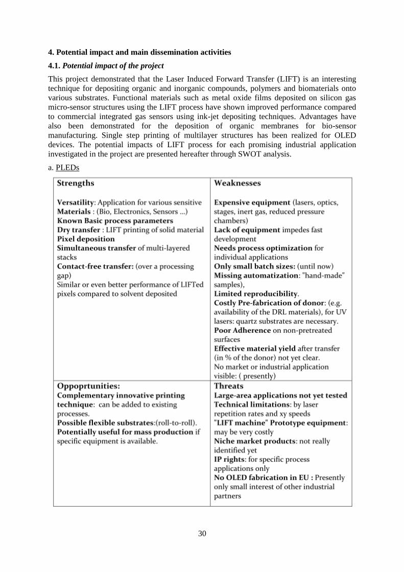
30
4. Potential impact and main dissemination activities
4.1. Potential impact of the project
This project demonstrated that the Laser Induced Forward Transfer (LIFT) is an interesting
technique for depositing organic and inorganic compounds, polymers and biomaterials onto
various substrates. Functional materials such as metal oxide films deposited on silicon gas
micro-sensor structures using the LIFT process have shown improved performance compared
to commercial integrated gas sensors using ink-jet depositing techniques. Advantages have
also been demonstrated for the deposition of organic membranes for bio-sensor
manufacturing. Single step printing of multilayer structures has been realized for OLED
devices. The potential impacts of LIFT process for each promising industrial application
investigated in the project are presented hereafter through SWOT analysis.
a. PLEDs
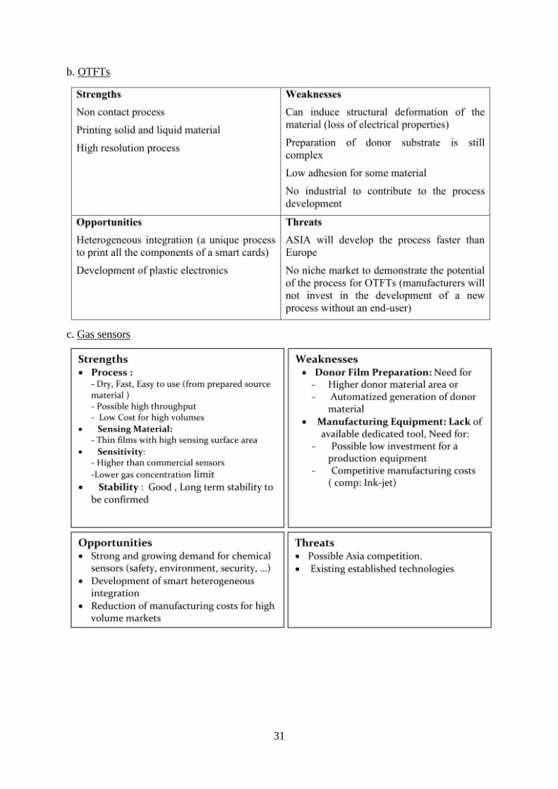
31
b. OTFTs
c. Gas sensors
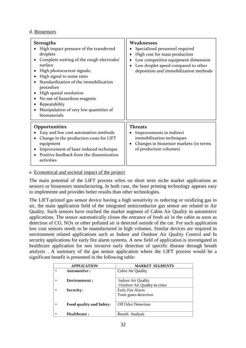
32
d. Biosensors
e. Economical and societal impact of the project
The main potential of the LIFT process relies on short term niche market applications as
sensors or biosensors manufacturing. In both case, the laser printing technology appears easy
to implemente and provides better results than other technologies.
The LIFT-printed gas sensor device having a high sensitivity to reducing or oxidizing gas in
air, the main application field of the integrated semiconductor gas sensor are related to Air
Quality. Such sensors have reached the market segment of Cabin Air Quality in automotive
applications. The sensor automatically closes the entrance of fresh air in the cabin as soon as
detection of CO, NOx or other polluted air is detected outside of the car. For such application
low cost sensors needs to be manufactured in high volumes. Similar devices are required in
environment related applications such as Indoor and Outdoor Air Quality Control and In
security applications for early fire alarm systems. A new field of application is investigated in
healthcare application for non invasive early detection of specific disease through breath
analysis . A summary of the gas sensor application where the LIFT process would be a
significant benefit is presented in the following table:
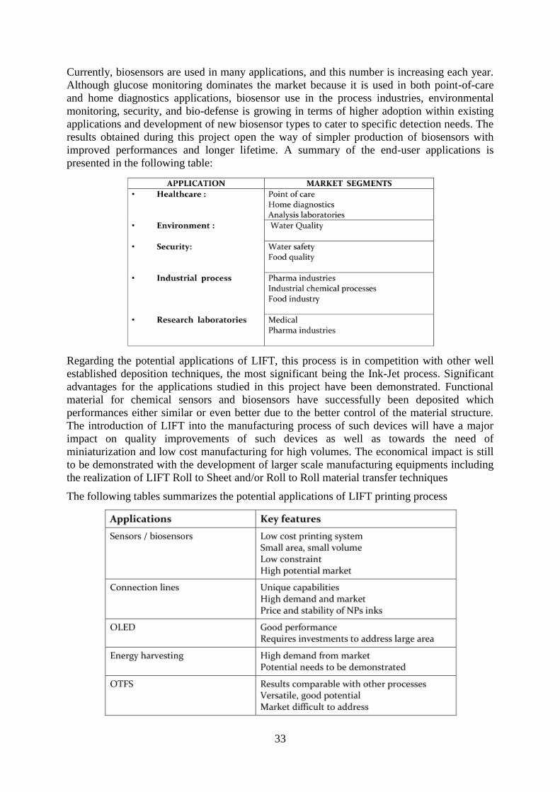
33
Currently, biosensors are used in many applications, and this number is increasing each year.
Although glucose monitoring dominates the market because it is used in both point-of-care
and home diagnostics applications, biosensor use in the process industries, environmental
monitoring, security, and bio-defense is growing in terms of higher adoption within existing
applications and development of new biosensor types to cater to specific detection needs. The
results obtained during this project open the way of simpler production of biosensors with
improved performances and longer lifetime. A summary of the end-user applications is
presented in the following table:
Regarding the potential applications of LIFT, this process is in competition with other well
established deposition techniques, the most significant being the Ink-Jet process. Significant
advantages for the applications studied in this project have been demonstrated. Functional
material for chemical sensors and biosensors have successfully been deposited which
performances either similar or even better due to the better control of the material structure.
The introduction of LIFT into the manufacturing process of such devices will have a major
impact on quality improvements of such devices as well as towards the need of
miniaturization and low cost manufacturing for high volumes. The economical impact is still
to be demonstrated with the development of larger scale manufacturing equipments including
the realization of LIFT Roll to Sheet and/or Roll to Roll material transfer techniques
The following tables summarizes the potential applications of LIFT printing process
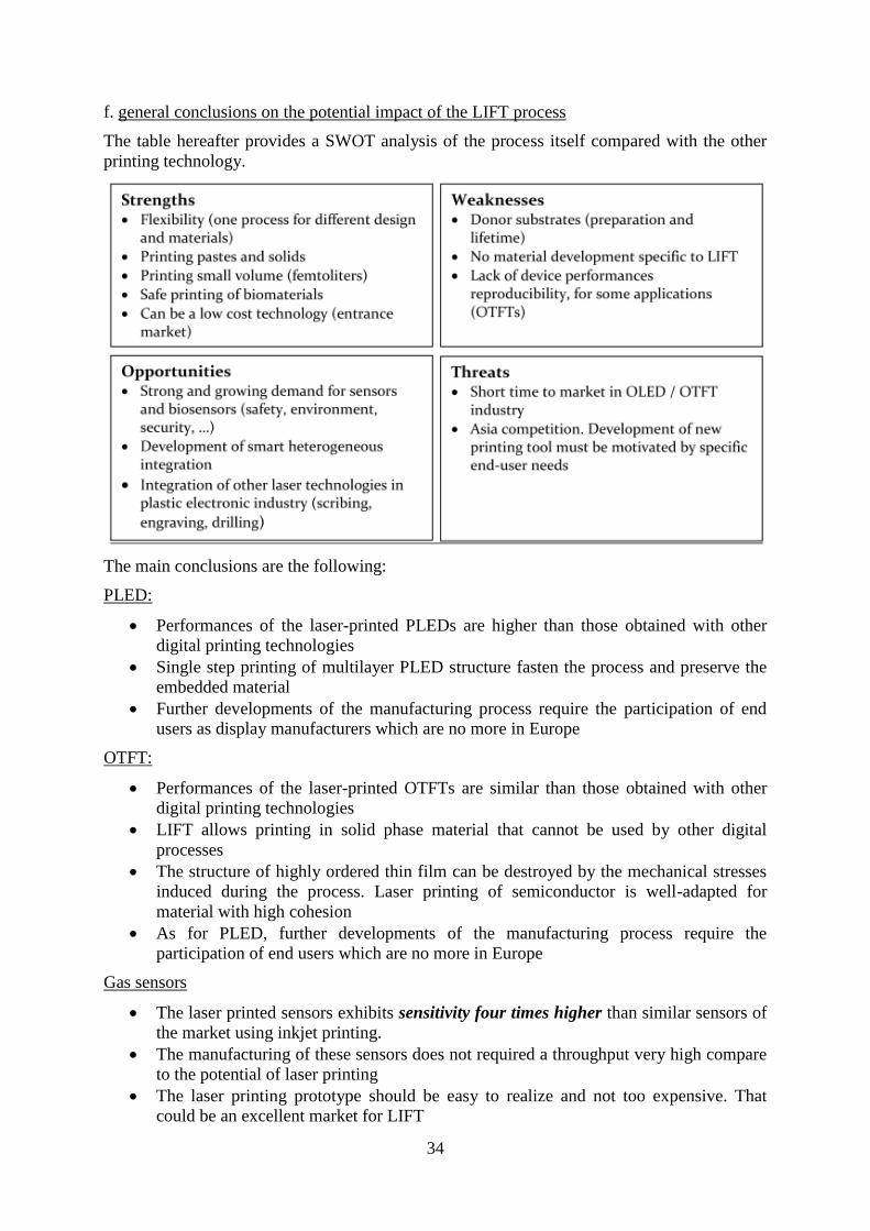
34
f. general conclusions on the potential impact of the LIFT process
The table hereafter provides a SWOT analysis of the process itself compared with the other
printing technology.
The main conclusions are the following:
PLED:
Performances of the laser-printed PLEDs are higher than those obtained with other
digital printing technologies
Single step printing of multilayer PLED structure fasten the process and preserve the
embedded material
Further developments of the manufacturing process require the participation of end
users as display manufacturers which are no more in Europe
OTFT:
Performances of the laser-printed OTFTs are similar than those obtained with other
digital printing technologies
LIFT allows printing in solid phase material that cannot be used by other digital
processes
The structure of highly ordered thin film can be destroyed by the mechanical stresses
induced during the process. Laser printing of semiconductor is well-adapted for
material with high cohesion
As for PLED, further developments of the manufacturing process require the
participation of end users which are no more in Europe
Gas sensors
The laser printed sensors exhibits sensitivity four times higher than similar sensors of
the market using inkjet printing.
The manufacturing of these sensors does not required a throughput very high compare
to the potential of laser printing
The laser printing prototype should be easy to realize and not too expensive. That
could be an excellent market for LIFT
35
The realization of the donor substrate is still complex for an industrial process.
Biosensors
Performances of laser printed biosensors are higher than those of other standard
sensors
As for sensors, the development of the laser based manufacturing tool appears to be
not too complex.
The market of biosensors does not required yet the development of a new technology
Energy harvesting
There are no other digital printing technologies of piezo or thermoelectric materials
The use of laser printing for thick and brittle materials is not suitable (cracks, break,
bad adhesion)
LIFT does not appears as the right technology for printing piezo or thermoelectric
materials
Printing conductive lines
LIFT allows printing metal nanoparticle (NPs) inks with a broad range of viscosities
Resolution higher than other digital printing process
Better control of thickness (100nm - 30m) and width (20m - 1mm) of the
conductive structures
LIFT allows printing pastes and 3D structures
The preparation of donor substrates need still to be improved
Laser printing appears as a very interesting technology for the realization of
connection lines and more generally for smart packaging applications
4.2 Dissemination activities
a. Towards the scientific community
The e-LIFT consortium had a strong action to promote the project towards the scientific
community. All along the project duration, partners wrote many publications, participate to a
large number of conferences and organised 9 workshops related to the project.
The key features for the overall project duration are the following:
51 publications in peer-review journals, 3 chapters of books and 11 proceedings of
conferences (50% are joint papers between e-LIFT partners)
36 invited talks in international conference.
56 oral presentations in international conferences (43% have joint authors between e-
LIFT partners).
42 poster presentations in national and international conferences (46% have joint
authors between e-LIFT partners).
13 invited seminars in international universities or workshops
e-LIFT consortium organized 9 special sessions on laser printing technologies in the frame of
international conferences
Organization of the EMRS 2010 spring meeting conference (Th. Lippert as general
chair). Organization of a special session on LIFT with 150 attendees (chairs I. Zergioti
and R. Eason). Strasbourg, France, June 7 -11, 2010
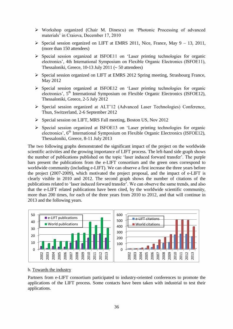
36
Workshop organized (Chair M. Dinescu) on ‘Photonic Processing of advanced
materials’ in Craiova, December 17, 2010
Special session organized on LIFT at EMRS 2011, Nice, France, May 9 – 13, 2011,
(more than 150 attendees)
Special session organized at ISFOE11 on ‘Laser printing technologies for organic
electronics’, 4th International Symposium on Flexible Organic Electronics (ISFOE11),
Thessaloniki, Greece, 10-13 July 2011 ( 50 attendees)
Special session organized on LIFT at EMRS 2012 Spring meeting, Strasbourg France,
May 2012
Special session organized at ISFOE12 on ‘Laser printing technologies for organic
electronics’, 5th International Symposium on Flexible Organic Electronics (ISFOE12),
Thessaloniki, Greece, 2-5 July 2012
Special session organized at ALT’12 (Advanced Laser Technologies) Conference,
Thun, Switzerland, 2-6 September 2012
Special session on LIFT, MRS Fall meeting, Boston US, Nov 2012
Special session organized at ISFOE13 on ‘Laser printing technologies for organic
electronics’, 6th
International Symposium on Flexible Organic Electronics (ISFOE12),
Thessaloniki, Greece, 8-11 July 2013
The two following graphs demonstrated the significant impact of the project on the worldwide
scientific activities and the growing importance of LIFT process. The left-hand side graph shows
the number of publications published on the topic ‘laser induced forward transfer’. The purple
bars present the publications from the e-LIFT consortium and the green ones correspond to
worldwide community (including e-LIFT). We can observe a first increase the three years before
the project (2007-2009), which motivated the project proposal, and the impact of e-LIFT is
clearly visible in 2010 and 2012. The second graph shows the number of citations of the
publications related to ‘laser induced forward transfer’. We can observe the same trends, and also
that the e-LIFT related publications have been cited, by the worldwide scientific community,
more than 200 times, for each of the three years from 2010 to 2012, and that will continue in
2013 and the following years.
b. Towards the industry
Partners from e-LIFT consortium participated to industry-oriented conferences to promote the
applications of the LIFT process. Some contacts have been taken with industrial to test their
applications.
0
10
20
30
40
50
20
02
20
03
20
04
20
05
20
06
20
07
20
08
20
09
20
10
20
11
20
12
20
13
e-LIFT publications
World publications
0
100
200
300
400
500
600
20
02
20
03
20
04
20
05
20
06
20
07
20
08
20
09
20
10
20
11
20
12
20
13
e-LIFT citations
World citations
37
International Conference and Exhibition for the Organic and Printed Electronics Industry
(LOPE-C), Frankfurt, Germany, May 31 - June 2, 2010
International Conference and Exhibition for the Organic and Printed Electronics Industry
(LOPE-C), Frankfurt, Germany, June 28-30, 2011
1st Swiss Conference on Printed Electronics and Functional Materials (Swiss-@print),
Basel, Switzerland, December 1-2, 2011
International Conference and Exhibition for the Organic and Printed Electronics Industry
(LOPE-C), Munchen, Germany, June 20-22, 2012
‘Innovative Printed Smart Objects’ Conference (IPSO), Gardanne, France, October 16 -
17, 2012
e-LIFT has also been presented at different companies like Philips, Orbotech, GEMALTO,
Genes’ink and Daetwyler graphics and to industrial consortium like ARCSIS and OPTITEC in
France or Solar Energy Solutions in Israel.
The e-LIFT project has also been presented to organizations which are in charge of valorisation
of research for industrial applications.
Carnot STAR which promotes industrial application in electronics and photonics.
SCS Clusters which promotes the industrial activities on Security aspects in
microelectronics
Optitec Clusters which promotes the industrial activities in Optics and Photonics
ARCIS cluster which promotes the activities on organic electronics in south of France
Solar Energy Solutions which invited the e-LIFT coordinator in Israel to present the
project in front of a large panel of industrials, and to visit during 3 days companies and
Universities.
c. Towards the General Public
The e-LIFT project has been presented to a public exhibition in Paris at the ‘Palais de la
Découverte’. A poster describing the project has been shown during four days (13-16 December,
2011) to the public visiting this exposition on laser applications.
Every year, from 2010 to 2013, the e-LIFT project has been presented to the general public
during two national open days for promotion of sciences (Fêtes de la sciences). This year a
special poster has been prepared to present the e-LIFT project and its societal applications
An article presenting the outcomes of e-LIFT has been published in a greek newspaper
The e-LIFT project has also been promoted through an article published in Public Services
Review and with large diffusion on their website. In this article, two paragraphs are dedicated to
the societal impact of the project.
An article on e-LIFT has been published on April 22nd
, 2013 in the French national daily
newspaper “les Echos” (150 000 copies per day). Even if the journalist wrote some mistakes
about the administrative features, he presented the societal impact of the project. The realization
of smart RFID tags to make easier the management of the products are mentioned as well as the
fabrication of medical sensors on wearable patches to facilitate the mobility of the patients.
(http://entrepreneur.lesechos.fr/entreprise/tendances/actualites/0202716773383-l-impression-
laser-dessine-le-futur-de-la-microelectronique-10028533.php).
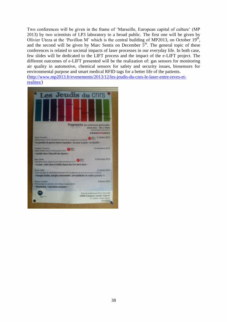
38
Two conferences will be given in the frame of ‘Marseille, European capital of culture’ (MP
2013) by two scientists of LP3 laboratory to a broad public. The first one will be given by
Olivier Uteza at the ‘Pavillon M’ which is the central building of MP2013, on October 19th
,
and the second will be given by Marc Sentis on December 5th
. The general topic of these
conferences is related to societal impacts of laser processes in our everyday life. In both case,
few slides will be dedicated to the LIFT process and the impact of the e-LIFT project. The
different outcomes of e-LIFT presented will be the realization of: gas sensors for monitoring
air quality in automotive, chemical sensors for safety and security issues, biosensors for
environmental purpose and smart medical RFID tags for a better life of the patients.
(http://www.mp2013.fr/evenements/2013/12/les-jeudis-du-cnrs-le-laser-entre-reves-et-
realites/)

39
5. e-LIFT CONTACTS AND INFORMATIONS
website: www.e-LIFT-project.eu
Coordination: CNRS – LP3 (FR) : www.lp3.univ-mrs.fr
Dr. Philippe Delaporte – [email protected]
Participants :
ARMINES / EMSE / CMP GC (FR) : http://www.emse.fr
Dr. Sébastien Sanaur – [email protected]
PSI (CH): www.psi.ch/en/
Dr. Thomas Lippert – [email protected]
EMPA (CH): http://www.empa.ch
Dr. Frank Nüesch - [email protected]
NTUA (EL): http://www.ntua.gr
Dr. Ioanna Zergioti - [email protected]
UB (ES): http://www.ub.edu
Dr. Pere Serra - [email protected]
US – ORC (UK): http://www.orc.soton.ac.uk
Professor Robert Eason - [email protected]
INFLPR (RO): http://www.inflpr.ro
Dr. Maria Dinescu - [email protected]
CNR – IDAC (IT): http://www.idasc.cnr.it
Dr. Enrico Verona - [email protected]
LML (UK): http://www.lasermicromachining.com
Dr. Nadeem Rizvi - [email protected]
ACXIS (FR): http://www.acxys.com
Dr. Thierry Sindzingre- [email protected]
MICROSENS (CH): http://www.microsens.ch
Dr. Alain Grisel - [email protected]
TAGSYS (FR): http://www.tagsysrfid.com
M. Christophe Loussert - [email protected]
BIOSENSOR (IT): http://www.biosensor.it
M. Giovanni Basile - [email protected]
TLI (FR): http://toplink-innovation.pagesperso-orange.fr
Dr. Alexandre Lorenzi - [email protected]
Grant Agreement number: 247868