Embed Size (px)
Citation preview
3075 Oakmead Village Drive | Santa Clara CA Ɩ 95051 | USA
+1.408.496.0222 www.promex-ind.com
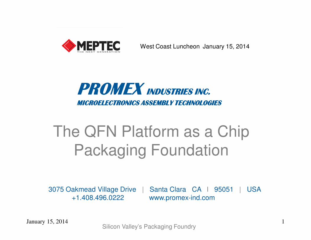
The QFN Platform as a Chip
Packaging Foundation
Silicon Valley’s Packaging Foundry
PROMEX PROMEX PROMEX PROMEX INDUSTRIES INC.INDUSTRIES INC.INDUSTRIES INC.INDUSTRIES INC.
MICROELECTRONICS MICROELECTRONICS MICROELECTRONICS MICROELECTRONICS ASSEMBLY ASSEMBLY ASSEMBLY ASSEMBLY TECHNOLOGIESTECHNOLOGIESTECHNOLOGIESTECHNOLOGIES
West Coast Luncheon January 15, 2014
January 15, 2014 1
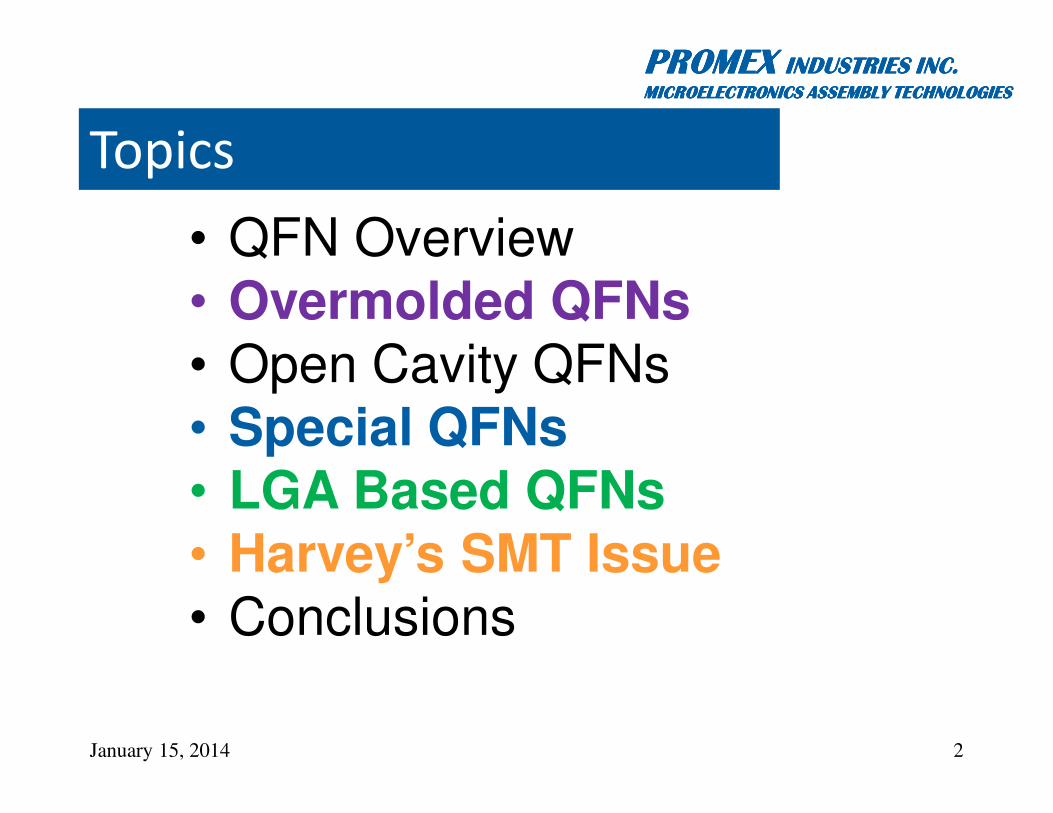
Topics
PROMEX PROMEX PROMEX PROMEX INDUSTRIES INC.INDUSTRIES INC.INDUSTRIES INC.INDUSTRIES INC.
MICROELECTRONICS ASSEMBLY TECHNOLOGIESMICROELECTRONICS ASSEMBLY TECHNOLOGIESMICROELECTRONICS ASSEMBLY TECHNOLOGIESMICROELECTRONICS ASSEMBLY TECHNOLOGIES
• QFN Overview
• Overmolded QFNs• Open Cavity QFNs
• Special QFNs• LGA Based QFNs• Harvey’s SMT Issue• Conclusions
January 15, 2014 2
QFN Overview
PROMEX PROMEX PROMEX PROMEX INDUSTRIES INC.INDUSTRIES INC.INDUSTRIES INC.INDUSTRIES INC.
MICROELECTRONICS ASSEMBLY TECHNOLOGIESMICROELECTRONICS ASSEMBLY TECHNOLOGIESMICROELECTRONICS ASSEMBLY TECHNOLOGIESMICROELECTRONICS ASSEMBLY TECHNOLOGIES
“The Package of Choice for
100 leads or less”
January 15, 2014 3
Foundation 1: A Versatile Platform
� � � � � �PROMEX PROMEX PROMEX INDUSTRIES INC.INDUSTRIES INC.INDUSTRIES INC.INDUSTRIES INC.
MICROELECTRONICS ASSEMBLY TECHNOLOGIESMICROELECTRONICS ASSEMBLY TECHNOLOGIESMICROELECTRONICS ASSEMBLY TECHNOLOGIESMICROELECTRONICS ASSEMBLY TECHNOLOGIESPlatform Versatility
Silicon Valley’s Packaging Foundry
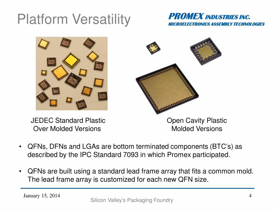
• QFNs, DFNs and LGAs are bottom terminated components (BTC’s) as described by the IPC Standard 7093 in which Promex participated.
• QFNs are built using a standard lead frame array that fits a common mold. The lead frame array is customized for each new QFN size.
JEDEC Standard Plastic Over Molded Versions
Open Cavity Plastic Molded Versions
January 15, 2014 4
� � � � � �� � � � � �� � � � � �� � � � � �� � � � �� � � ��INDUSTRIES INC.INDUSTRIES INC.INDUSTRIES INC.
MICROELECTRONICS ASSEMBLY TECHNOLOGIESMICROELECTRONICS ASSEMBLY TECHNOLOGIESMICROELECTRONICS ASSEMBLY TECHNOLOGIESMICROELECTRONICS ASSEMBLY TECHNOLOGIESJEDEC QFN / DFN
Silicon Valley’s Packaging Foundry
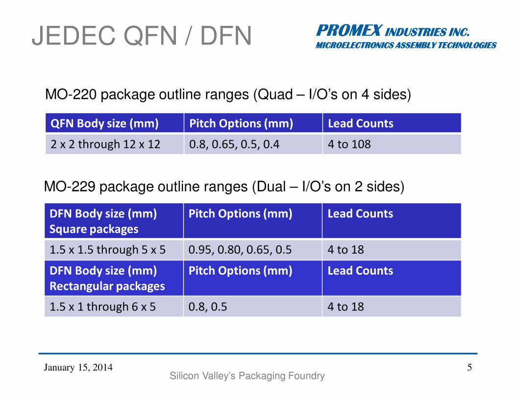
QFN Body size (mm) Pitch Options (mm) Lead Counts
2 x 2 through 12 x 12 0.8, 0.65, 0.5, 0.4 4 to 108
MO-220 package outline ranges (Quad – I/O’s on 4 sides)
DFN Body size (mm)
Square packages
Pitch Options (mm) Lead Counts
1.5 x 1.5 through 5 x 5 0.95, 0.80, 0.65, 0.5 4 to 18
DFN Body size (mm)
Rectangular packages
Pitch Options (mm) Lead Counts
1.5 x 1 through 6 x 5 0.8, 0.5 4 to 18
MO-229 package outline ranges (Dual – I/O’s on 2 sides)
January 15, 2014 5
� � � � � �� � � � � �� � � � � �� � � � � �� � � � �� � � ��� � � � �� � � ��� � � � �� � � ��� � � � �� � � ��� � � � � � � � � � � � � � � � � � � � � � � � � � � � � � � � � � � �MICROELECTRONICS ASSEMBLY TECHNOLOGIESMICROELECTRONICS ASSEMBLY TECHNOLOGIESMICROELECTRONICS ASSEMBLY TECHNOLOGIES
Promex tooled sizes
Silicon Valley’s Packaging Foundry
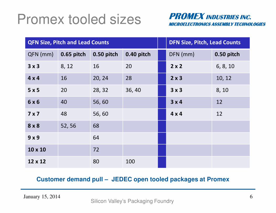
Customer demand pull – JEDEC open tooled packages at Promex
QFN Size, Pitch and Lead Counts DFN Size, Pitch, Lead Counts
QFN (mm) 0.65 pitch 0.50 pitch 0.40 pitch DFN (mm) 0.50 pitch
3 x 3 8, 12 16 20 2 x 2 6, 8, 10
4 x 4 16 20, 24 28 2 x 3 10, 12
5 x 5 20 28, 32 36, 40 3 x 3 8, 10
6 x 6 40 56, 60 3 x 4 12
7 x 7 48 56, 60 4 x 4 12
8 x 8 52, 56 68
9 x 9 64
10 x 10 72
12 x 12 80 100
January 15, 2014 6
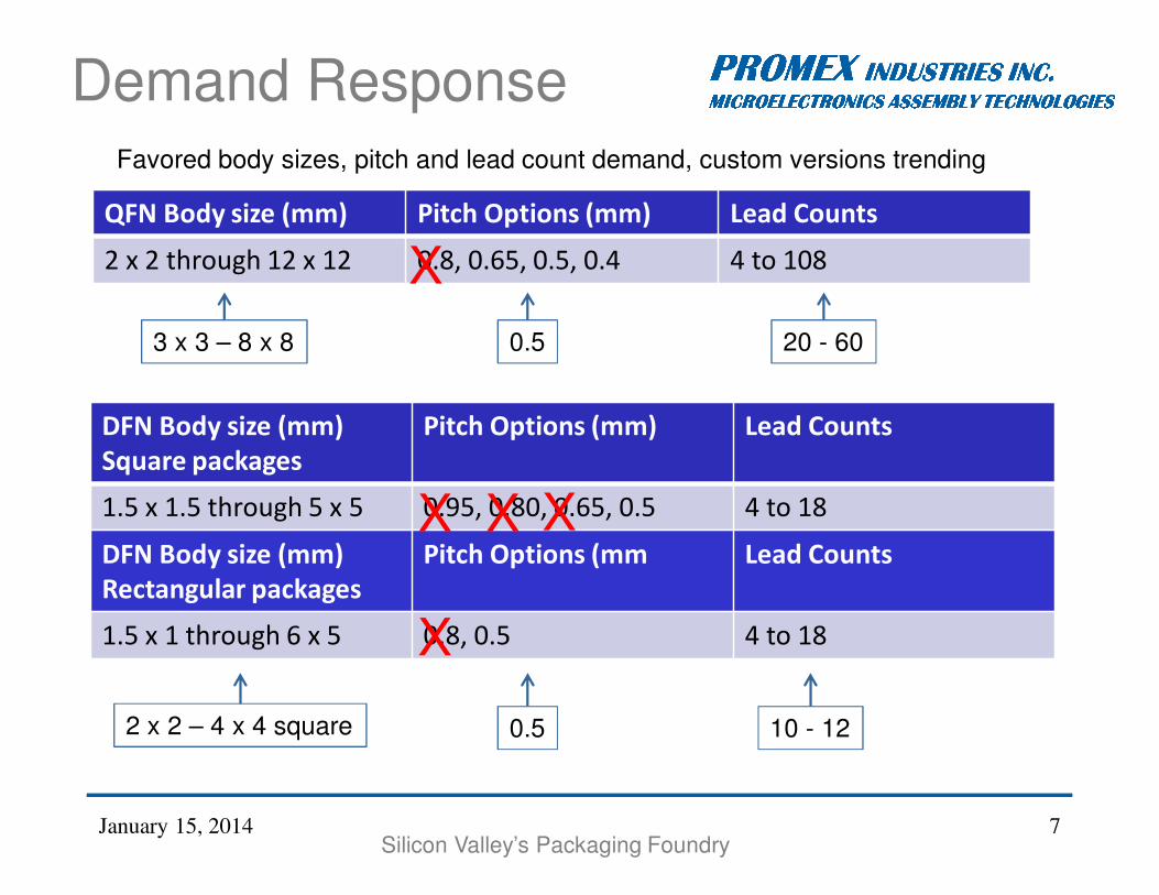
� � � � � �� � � � � �� � � � � �� � � � � �� � � � �� � � ��� � � � �� � � ��� � � � �� � � ��� � � � �� � � ��� � � � � � � � � � � � � � � � � � � � � � � � � � � � � � � � � � � �� � � � � � � � � � � � � � � � � � � � � � � � � � � � � � � � � � � �� � � � � � � � � � � � � � � � � � � � � � � � � � � � � � � � � � � �� � � � � � � � � � � � � � � � � � � � � � � � � � � � � � � � � � � �Demand Response
Silicon Valley’s Packaging Foundry
QFN Body size (mm) Pitch Options (mm) Lead Counts
2 x 2 through 12 x 12 0.8, 0.65, 0.5, 0.4 4 to 108
3 x 3 – 8 x 8 0.5 20 - 60
DFN Body size (mm)
Square packages
Pitch Options (mm) Lead Counts
1.5 x 1.5 through 5 x 5 0.95, 0.80, 0.65, 0.5 4 to 18
DFN Body size (mm)
Rectangular packages
Pitch Options (mm Lead Counts
1.5 x 1 through 6 x 5 0.8, 0.5 4 to 18
2 x 2 – 4 x 4 square 0.5 10 - 12
Favored body sizes, pitch and lead count demand, custom versions trending
X
X
X X X
January 15, 2014 7
� � � � � �� � � � � �� � � � � �� � � � � �� � � � �� � � ��� � � � �� � � ��� � � � �� � � ��� � � � �� � � ��� � � � � � � � � � � � � � � � � � � � � � � � � � � � � � � � � � � �� � � � � � � � � � � � � � � � � � � � � � � � � � � � � � � � � � � �� � � � � � � � � � � � � � � � � � � � � � � � � � � � � � � � � � � �� � � � � � � � � � � � � � � � � � � � � � � � � � � � � � � � � � � �QFN Platform
Advantages
Silicon Valley’s Packaging Foundry
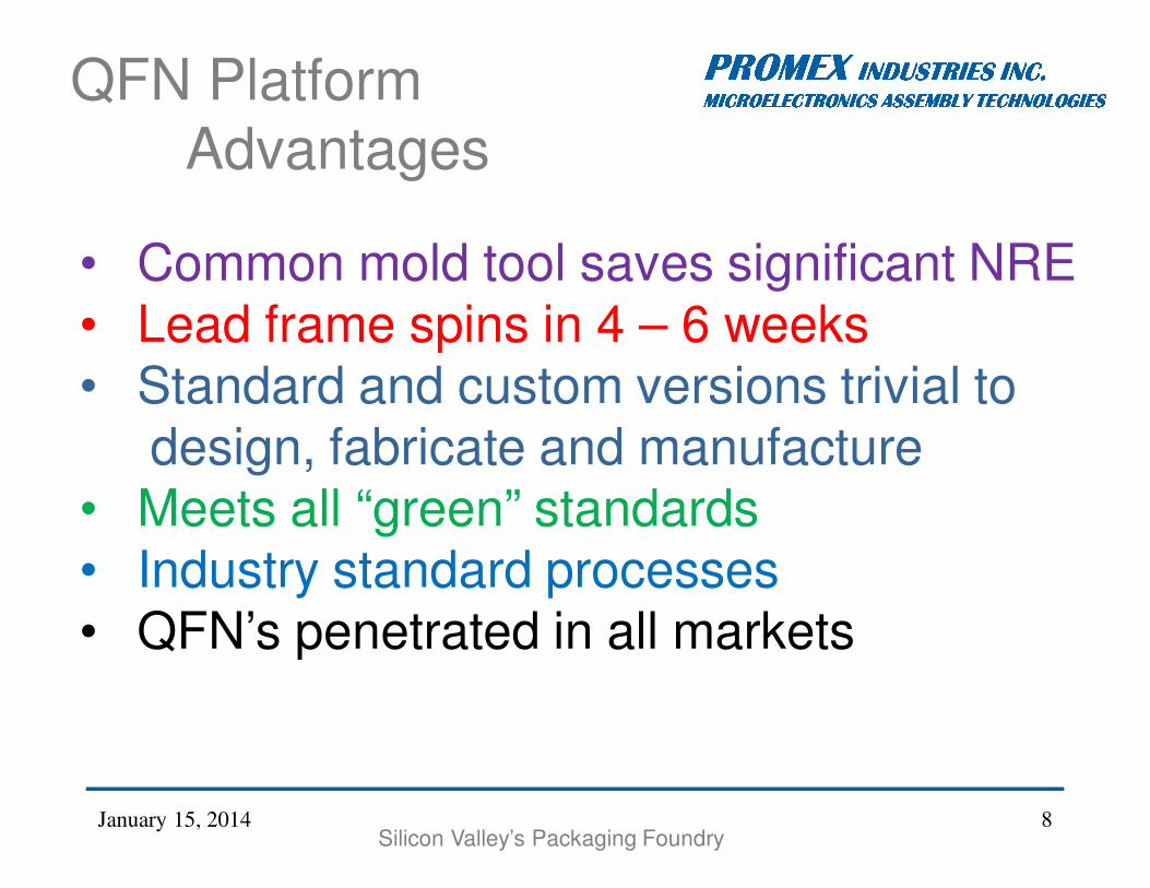
• Common mold tool saves significant NRE• Lead frame spins in 4 – 6 weeks• Standard and custom versions trivial to
design, fabricate and manufacture• Meets all “green” standards• Industry standard processes• QFN’s penetrated in all markets
January 15, 2014 8
Overmolded QFNs
PROMEX PROMEX PROMEX PROMEX INDUSTRIES INC.INDUSTRIES INC.INDUSTRIES INC.INDUSTRIES INC.
MICROELECTRONICS ASSEMBLY TECHNOLOGIESMICROELECTRONICS ASSEMBLY TECHNOLOGIESMICROELECTRONICS ASSEMBLY TECHNOLOGIESMICROELECTRONICS ASSEMBLY TECHNOLOGIES
January 15, 2014 9
Foundation 2: Easily Modified
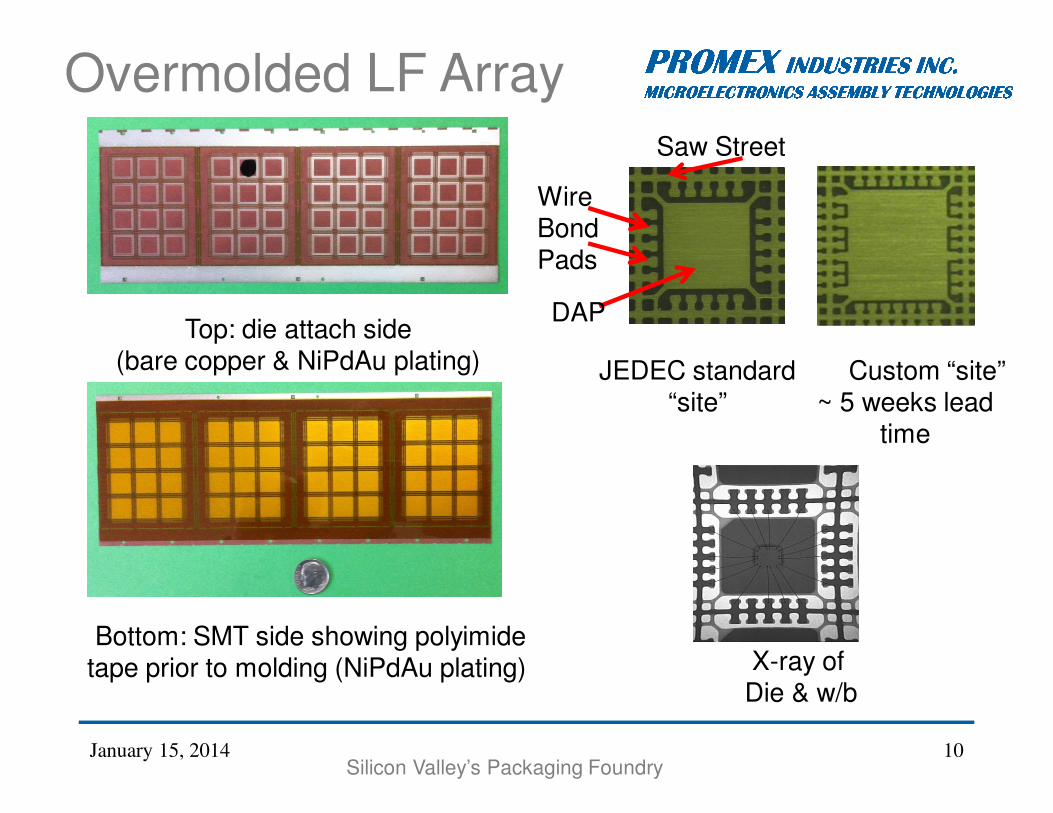
� � � � � �� � � � � �� � � � � �� � � � � �� � � � �� � � ��� � � � �� � � ��� � � � �� � � ��� � � � �� � � ��� � � � � � � � � � � � � � � � � � � � � � � � � � � � � � � � � � � �� � � � � � � � � � � � � � � � � � � � � � � � � � � � � � � � � � � �� � � � � � � � � � � � � � � � � � � � � � � � � � � � � � � � � � � �� � � � � � � � � � � � � � � � � � � � � � � � � � � � � � � � � � � �Overmolded LF Array
Silicon Valley’s Packaging Foundry
Top: die attach side(bare copper & NiPdAu plating)
Bottom: SMT side showing polyimide tape prior to molding (NiPdAu plating)
Custom “site”~ 5 weeks lead
time
JEDEC standard“site”
DAP
Wire BondPads
Saw Street
X-ray ofDie & w/b
January 15, 2014 10
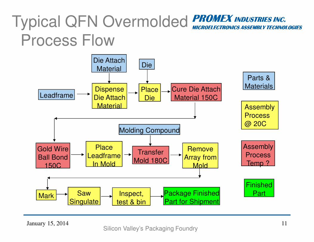
� � � � � �� � � � � �� � � � � �� � � � � �� � � � �� � � ��� � � � �� � � ��� � � � �� � � ��� � � � �� � � ��� � � � � � � � � � � � � � � � � � � � � � � � � � � � � � � � � � � �� � � � � � � � � � � � � � � � � � � � � � � � � � � � � � � � � � � �� � � � � � � � � � � � � � � � � � � � � � � � � � � � � � � � � � � �� � � � � � � � � � � � � � � � � � � � � � � � � � � � � � � � � � � �Typical QFN Overmolded
Process Flow
Silicon Valley’s Packaging FoundryJanuary 15, 2014 11
LeadframePlace
Die
Cure Die Attach
Material 150C
Die
Dispense
Die Attach
Material
Transfer
Mold 180C
Place
Leadframe
In Mold
Gold Wire
Ball Bond
150C
Remove
Array from
Mold
Saw
SingulateMark Package Finished
Part for Shipment
Die Attach
Material
Molding Compound
Parts &
Materials
Assembly
Process
@ 20C
Assembly
Process
Temp ?
Finished
PartInspect,
test & bin
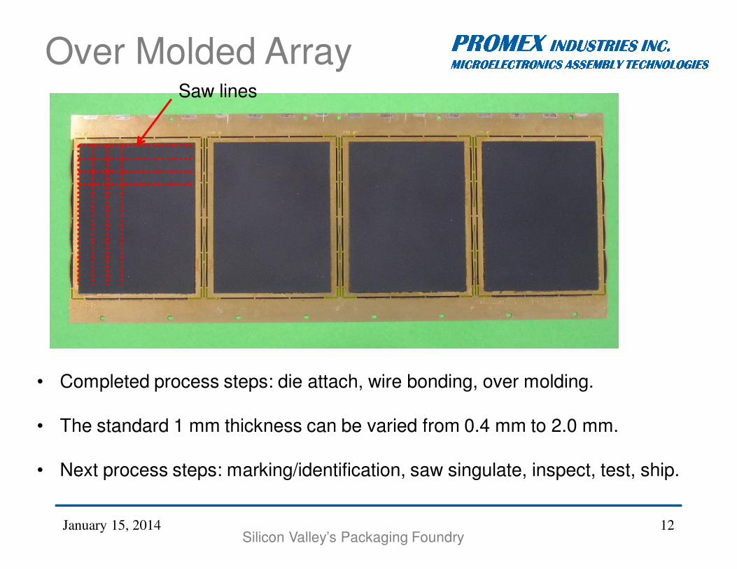
� � � � � �� � � � � �� � � � � �� � � � � �� � � � �� � � ��� � � � �� � � ��� � � � �� � � ��� � � � �� � � ��� � � � � � � � � � � � � � � � � � � � � � � � � � � � � � � � � � � �� � � � � � � � � � � � � � � � � � � � � � � � � � � � � � � � � � � �� � � � � � � � � � � � � � � � � � � � � � � � � � � � � � � � � � � �� � � � � � � � � � � � � � � � � � � � � � � � � � � � � � � � � � � �Over Molded Array
Silicon Valley’s Packaging Foundry
• Completed process steps: die attach, wire bonding, over molding.
• The standard 1 mm thickness can be varied from 0.4 mm to 2.0 mm.
• Next process steps: marking/identification, saw singulate, inspect, test, ship.
January 15, 2014 12
Saw lines
Open Cavity QFNs
PROMEX PROMEX PROMEX PROMEX INDUSTRIES INC.INDUSTRIES INC.INDUSTRIES INC.INDUSTRIES INC.
MICROELECTRONICS ASSEMBLY TECHNOLOGIESMICROELECTRONICS ASSEMBLY TECHNOLOGIESMICROELECTRONICS ASSEMBLY TECHNOLOGIESMICROELECTRONICS ASSEMBLY TECHNOLOGIES
January 15, 2014 13
Foundation 3: A Versatile Alternate
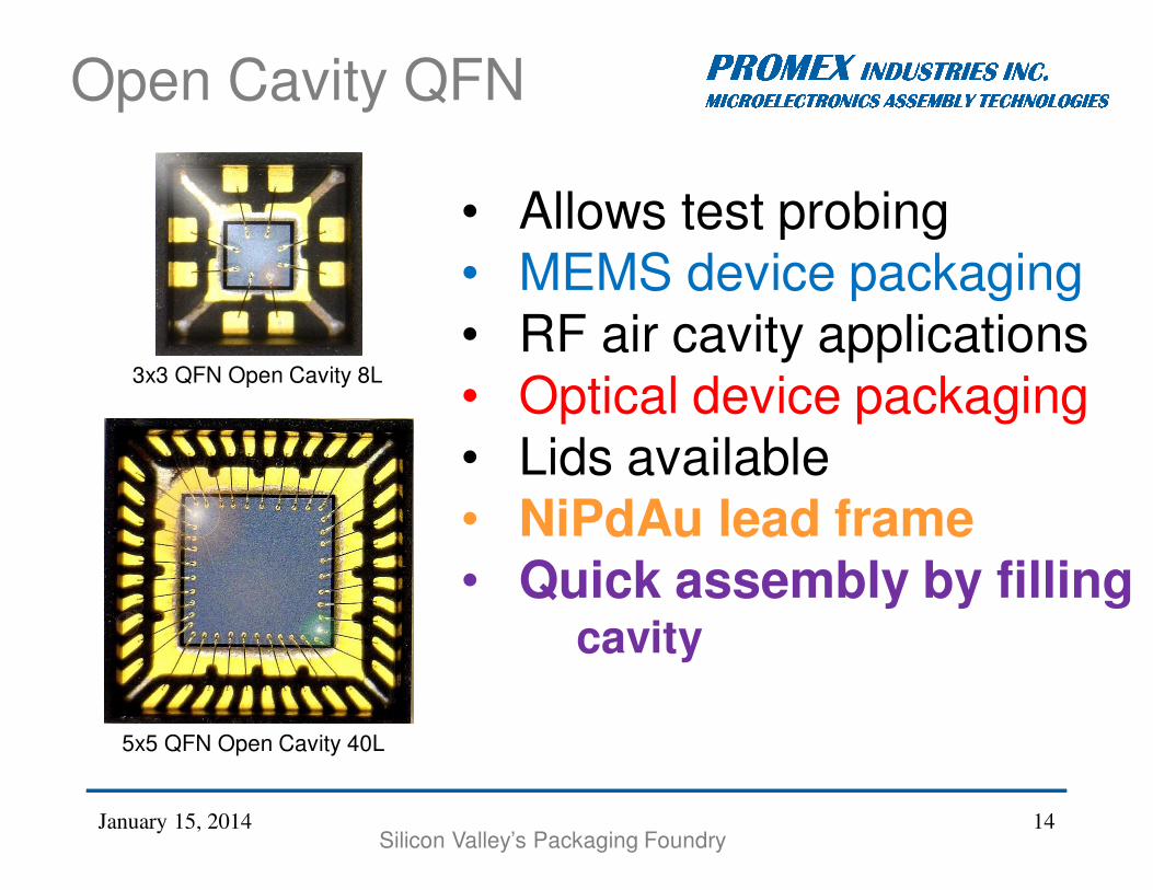
� � � � � �� � � � � �� � � � � �� � � � � �� � � � �� � � ��� � � � �� � � ��� � � � �� � � ��� � � � �� � � ��� � � � � � � � � � � � � � � � � � � � � � � � � � � � � � � � � � � �� � � � � � � � � � � � � � � � � � � � � � � � � � � � � � � � � � � �� � � � � � � � � � � � � � � � � � � � � � � � � � � � � � � � � � � �� � � � � � � � � � � � � � � � � � � � � � � � � � � � � � � � � � � �Open Cavity QFN
Silicon Valley’s Packaging Foundry
3x3 QFN Open Cavity 8L
5x5 QFN Open Cavity 40L
• Allows test probing• MEMS device packaging• RF air cavity applications• Optical device packaging• Lids available• NiPdAu lead frame• Quick assembly by filling
cavity
January 15, 2014 14
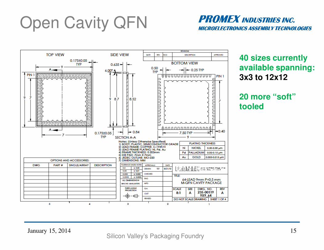
� � � � � �� � � � � �� � � � � �� � � � � �� � � � �� � � ��� � � � �� � � ��� � � � �� � � ��� � � � �� � � ��� � � � � � � � � � � � � � � � � � � � � � � � � � � � � � � � � � � �� � � � � � � � � � � � � � � � � � � � � � � � � � � � � � � � � � � �� � � � � � � � � � � � � � � � � � � � � � � � � � � � � � � � � � � �� � � � � � � � � � � � � � � � � � � � � � � � � � � � � � � � � � � �Open Cavity QFN
Silicon Valley’s Packaging Foundry
40 sizes currently available spanning:3x3 to 12x12
20 more “soft”tooled
January 15, 2014 15
� � � � � �� � � � � �� � � � � �� � � � � �� � � � �� � � ��� � � � �� � � ��� � � � �� � � ��� � � � �� � � ��� � � � � � � � � � � � � � � � � � � � � � � � � � � � � � � � � � � �� � � � � � � � � � � � � � � � � � � � � � � � � � � � � � � � � � � �� � � � � � � � � � � � � � � � � � � � � � � � � � � � � � � � � � � �� � � � � � � � � � � � � � � � � � � � � � � � � � � � � � � � � � � �Open Cavity Availability
Silicon Valley’s Packaging FoundryJanuary 15, 2014 16
• Off-the-Shelf from:• www.mirrorsemi.com
• Web site has many “tools”
• available sizes
• variety of drawings
• Lids
• Etc.
� � � � � �� � � � � �� � � � � �� � � � � �� � � � �� � � ��� � � � �� � � ��� � � � �� � � ��� � � � �� � � ��� � � � � � � � � � � � � � � � � � � � � � � � � � � � � � � � � � � �� � � � � � � � � � � � � � � � � � � � � � � � � � � � � � � � � � � �� � � � � � � � � � � � � � � � � � � � � � � � � � � � � � � � � � � �� � � � � � � � � � � � � � � � � � � � � � � � � � � � � � � � � � � �
Package Performance
MSL & Parastic Properties
January 15, 2014 17
Foundation 4: Performance
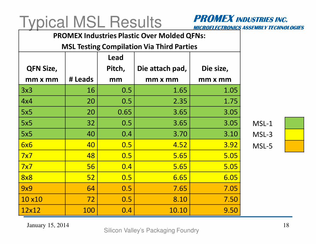
� � � � � �� � � � � �� � � � � �� � � � � �� � � � �� � � ��� � � � �� � � ��� � � � �� � � ��� � � � �� � � ��� � � � � � � � � � � � � � � � � � � � � � � � � � � � � � � � � � � �� � � � � � � � � � � � � � � � � � � � � � � � � � � � � � � � � � � �� � � � � � � � � � � � � � � � � � � � � � � � � � � � � � � � � � � �� � � � � � � � � � � � � � � � � � � � � � � � � � � � � � � � � � � �Typical MSL Results
Silicon Valley’s Packaging Foundry
PROMEX Industries Plastic Over Molded QFNs:
MSL Testing Compilation Via Third Parties
QFN Size,
mm x mm # Leads
Lead
Pitch,
mm
Die attach pad,
mm x mm
Die size,
mm x mm
3x3 16 0.5 1.65 1.05
4x4 20 0.5 2.35 1.75
5x5 20 0.65 3.65 3.05
5x5 32 0.5 3.65 3.05
5x5 40 0.4 3.70 3.10
6x6 40 0.5 4.52 3.92
7x7 48 0.5 5.65 5.05
7x7 56 0.4 5.65 5.05
8x8 52 0.5 6.65 6.05
9x9 64 0.5 7.65 7.05
10 x10 72 0.5 8.10 7.50
12x12 100 0.4 10.10 9.50
MSL-1
MSL-3
MSL-5
January 15, 2014 18
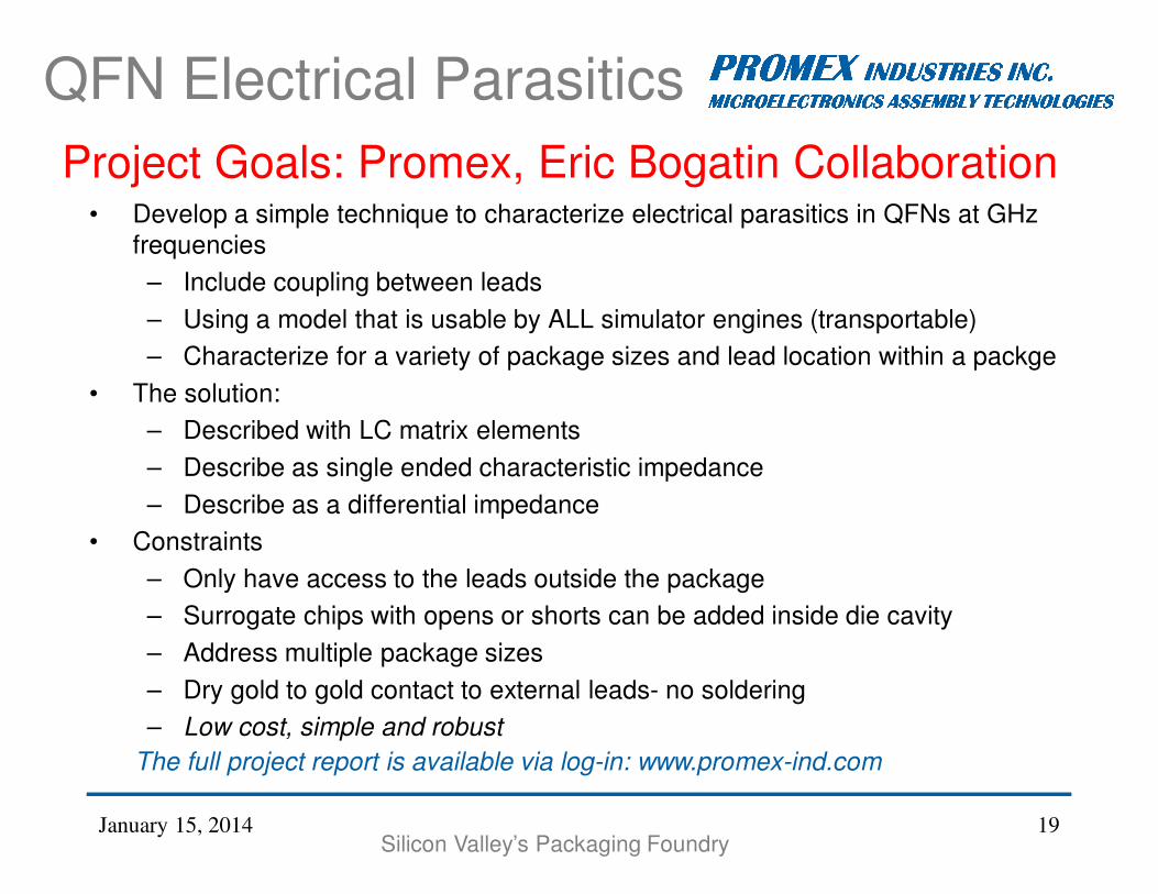
� � � � � �� � � � � �� � � � � �� � � � � �� � � � �� � � ��� � � � �� � � ��� � � � �� � � ��� � � � �� � � ��� � � � � � � � � � � � � � � � � � � � � � � � � � � � � � � � � � � �� � � � � � � � � � � � � � � � � � � � � � � � � � � � � � � � � � � �� � � � � � � � � � � � � � � � � � � � � � � � � � � � � � � � � � � �� � � � � � � � � � � � � � � � � � � � � � � � � � � � � � � � � � � �QFN Electrical Parasitics
Silicon Valley’s Packaging Foundry
• Develop a simple technique to characterize electrical parasitics in QFNs at GHz
frequencies
– Include coupling between leads
– Using a model that is usable by ALL simulator engines (transportable)
– Characterize for a variety of package sizes and lead location within a packge
• The solution:
– Described with LC matrix elements
– Describe as single ended characteristic impedance
– Describe as a differential impedance
• Constraints
– Only have access to the leads outside the package
– Surrogate chips with opens or shorts can be added inside die cavity
– Address multiple package sizes
– Dry gold to gold contact to external leads- no soldering
– Low cost, simple and robust
Project Goals: Promex, Eric Bogatin Collaboration
The full project report is available via log-in: www.promex-ind.com
January 15, 2014 19
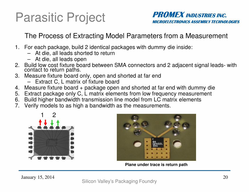
� � � � � �� � � � � �� � � � � �� � � � � �� � � � �� � � ��� � � � �� � � ��� � � � �� � � ��� � � � �� � � ��� � � � � � � � � � � � � � � � � � � � � � � � � � � � � � � � � � � �� � � � � � � � � � � � � � � � � � � � � � � � � � � � � � � � � � � �� � � � � � � � � � � � � � � � � � � � � � � � � � � � � � � � � � � �� � � � � � � � � � � � � � � � � � � � � � � � � � � � � � � � � � � �Parasitic Project
Silicon Valley’s Packaging Foundry
The Process of Extracting Model Parameters from a Measurement
1. For each package, build 2 identical packages with dummy die inside: – At die, all leads shorted to return – At die, all leads open
2. Build low cost fixture board between SMA connectors and 2 adjacent signal leads- with contact to return paths.
3. Measure fixture board only, open and shorted at far end– Extract C, L matrix of fixture board
4. Measure fixture board + package open and shorted at far end with dummy die5. Extract package only C, L matrix elements from low frequency measurement6. Build higher bandwidth transmission line model from LC matrix elements7. Verify models to as high a bandwidth as the measurements.
1 2
Plane under trace is return path
January 15, 2014 20
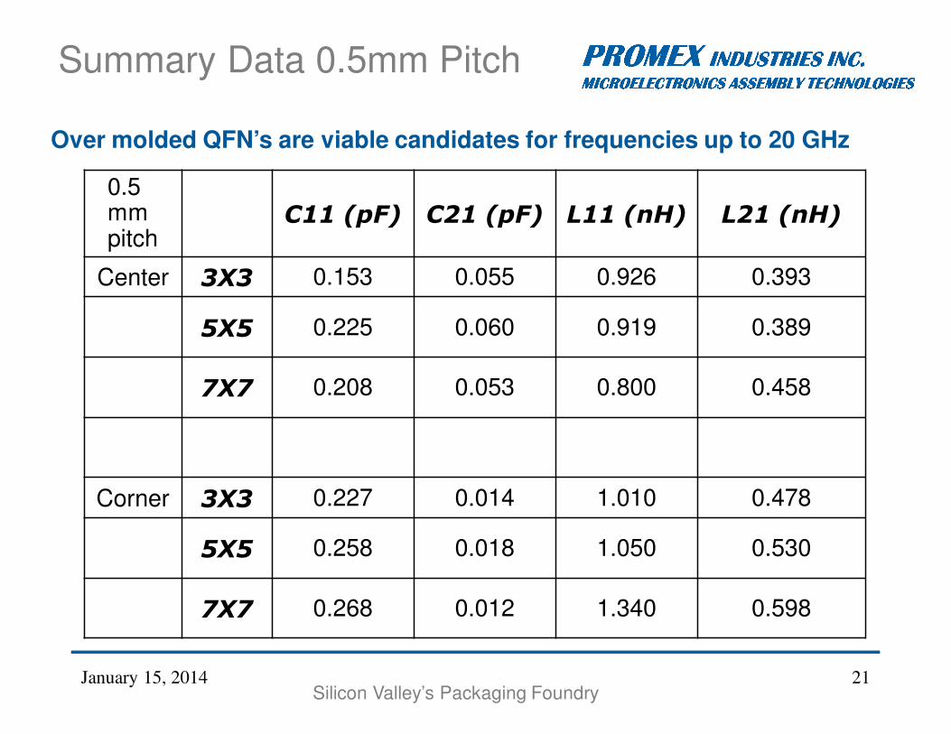
� � � � � �� � � � � �� � � � � �� � � � � �� � � � �� � � ��� � � � �� � � ��� � � � �� � � ��� � � � �� � � ��� � � � � � � � � � � � � � � � � � � � � � � � � � � � � � � � � � � �� � � � � � � � � � � � � � � � � � � � � � � � � � � � � � � � � � � �� � � � � � � � � � � � � � � � � � � � � � � � � � � � � � � � � � � �� � � � � � � � � � � � � � � � � � � � � � � � � � � � � � � � � � � �Summary Data 0.5mm Pitch
Silicon Valley’s Packaging Foundry
0.5 mm pitch
C11 (pF) C21 (pF) L11 (nH) L21 (nH)
Center 3X3 0.153 0.055 0.926 0.393
5X5 0.225 0.060 0.919 0.389
7X7 0.208 0.053 0.800 0.458
Corner 3X3 0.227 0.014 1.010 0.478
5X5 0.258 0.018 1.050 0.530
7X7 0.268 0.012 1.340 0.598
Over molded QFN’s are viable candidates for frequencies up to 20 GHz
January 15, 2014 21
� � � � � �� � � � � �� � � � � �� � � � � �� � � � �� � � ��� � � � �� � � ��� � � � �� � � ��� � � � �� � � ��� � � � � � � � � � � � � � � � � � � � � � � � � � � � � � � � � � � �� � � � � � � � � � � � � � � � � � � � � � � � � � � � � � � � � � � �� � � � � � � � � � � � � � � � � � � � � � � � � � � � � � � � � � � �� � � � � � � � � � � � � � � � � � � � � � � � � � � � � � � � � � � �
Advanced PackagingFoundation 5: Platform & Process Leverage
January 15, 2014 22
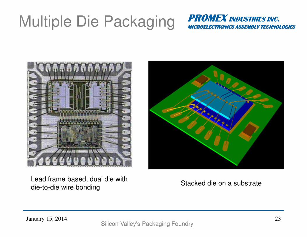
Multiple Die Packaging PROMEX PROMEX PROMEX PROMEX INDUSTRIES INC.INDUSTRIES INC.INDUSTRIES INC.INDUSTRIES INC.
MICROELECTRONICS ASSEMBLY TECHNOLOGIESMICROELECTRONICS ASSEMBLY TECHNOLOGIESMICROELECTRONICS ASSEMBLY TECHNOLOGIESMICROELECTRONICS ASSEMBLY TECHNOLOGIES
Silicon Valley’s Packaging Foundry
Lead frame based, dual die with
die-to-die wire bondingStacked die on a substrate
January 15, 2014 23
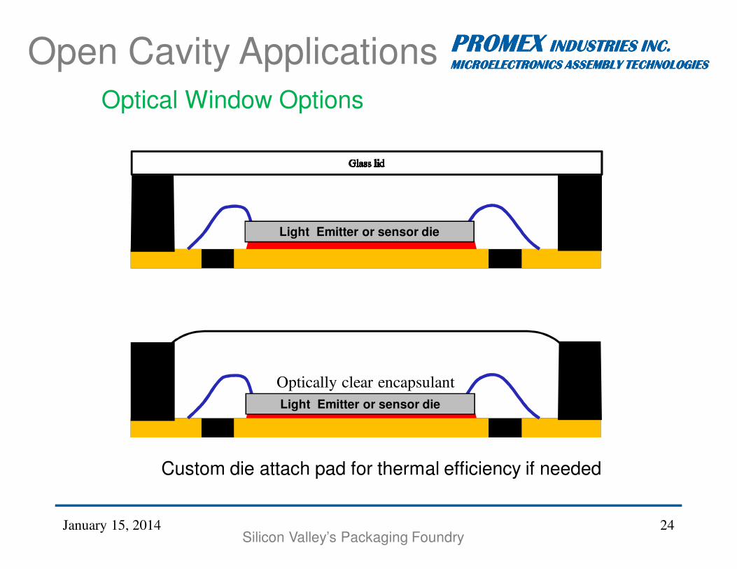
Open Cavity Applications
Optical Window Options
PROMEX PROMEX PROMEX PROMEX INDUSTRIES INC.INDUSTRIES INC.INDUSTRIES INC.INDUSTRIES INC.
MICROELECTRONICS ASSEMBLY TECHNOLOGIESMICROELECTRONICS ASSEMBLY TECHNOLOGIESMICROELECTRONICS ASSEMBLY TECHNOLOGIESMICROELECTRONICS ASSEMBLY TECHNOLOGIES
Silicon Valley’s Packaging Foundry
Custom die attach pad for thermal efficiency if needed
January 15, 2014 24
Optically clear encapsulant
Light Emitter or sensor die
Light Emitter or sensor die
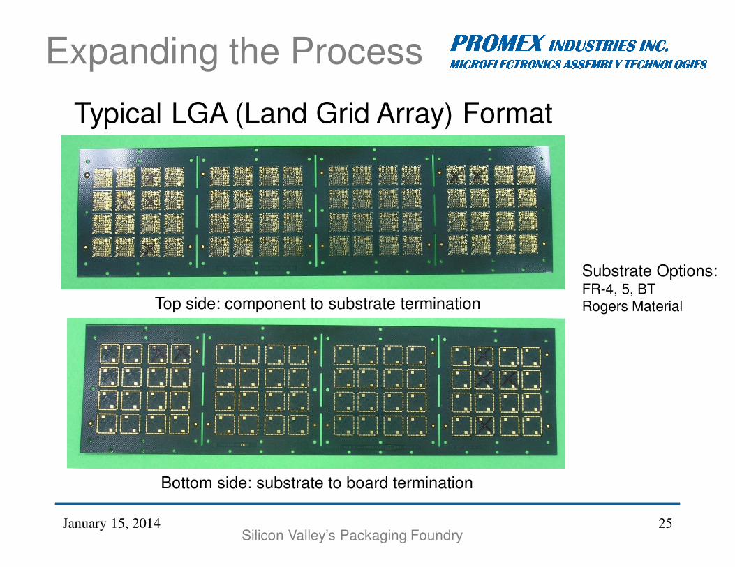
� � � � � �� � � � � �� � � � � �� � � � � �� � � � �� � � ��� � � � �� � � ��� � � � �� � � ��� � � � �� � � ��� � � � � � � � � � � � � � � � � � � � � � � � � � � � � � � � � � � �� � � � � � � � � � � � � � � � � � � � � � � � � � � � � � � � � � � �� � � � � � � � � � � � � � � � � � � � � � � � � � � � � � � � � � � �� � � � � � � � � � � � � � � � � � � � � � � � � � � � � � � � � � � �Expanding the Process
Silicon Valley’s Packaging Foundry
Bottom side: substrate to board termination
Top side: component to substrate termination
Typical LGA (Land Grid Array) Format
Substrate Options:FR-4, 5, BT
Rogers Material
January 15, 2014 25
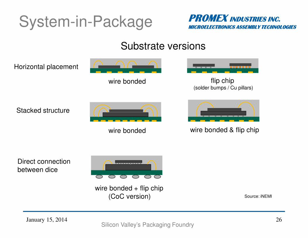
System-in-Package PROMEX PROMEX PROMEX PROMEX INDUSTRIES INC.INDUSTRIES INC.INDUSTRIES INC.INDUSTRIES INC.
MICROELECTRONICS ASSEMBLY TECHNOLOGIESMICROELECTRONICS ASSEMBLY TECHNOLOGIESMICROELECTRONICS ASSEMBLY TECHNOLOGIESMICROELECTRONICS ASSEMBLY TECHNOLOGIES
Silicon Valley’s Packaging Foundry
Source: iNEMI
wire bonded flip chip (solder bumps / Cu pillars)
Horizontal placement
Stacked structure
wire bonded wire bonded & flip chip
Direct connection
between dice
wire bonded + flip chip
(CoC version)
Substrate versions
January 15, 2014 26
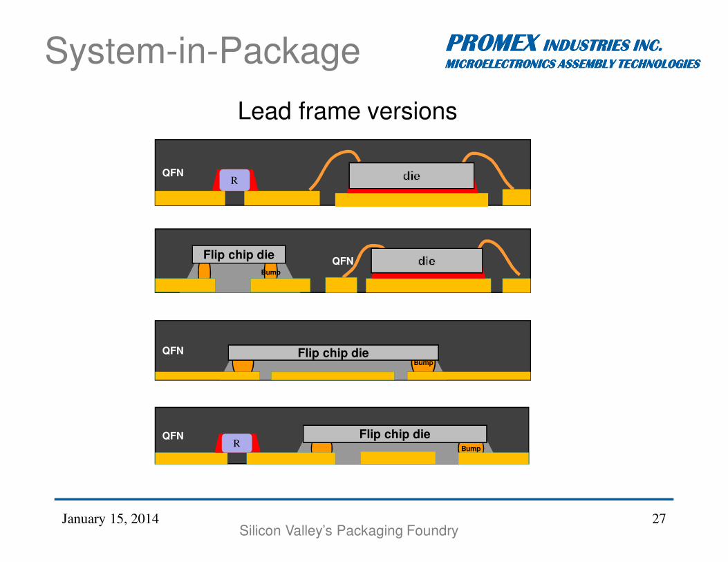
System-in-Package PROMEX PROMEX PROMEX PROMEX INDUSTRIES INC.INDUSTRIES INC.INDUSTRIES INC.INDUSTRIES INC.
MICROELECTRONICS ASSEMBLY TECHNOLOGIESMICROELECTRONICS ASSEMBLY TECHNOLOGIESMICROELECTRONICS ASSEMBLY TECHNOLOGIESMICROELECTRONICS ASSEMBLY TECHNOLOGIES
Silicon Valley’s Packaging Foundry
QFNBump
Flip chip die
QFNR
Bump
Flip chip die
QFNBump
Flip chip die
QFNR
Lead frame versions
January 15, 2014 27
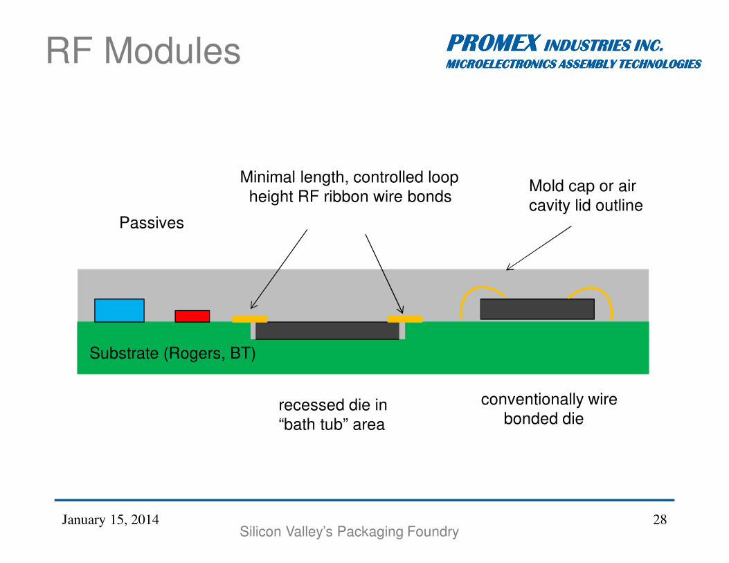
RF Modules PROMEX PROMEX PROMEX PROMEX INDUSTRIES INC.INDUSTRIES INC.INDUSTRIES INC.INDUSTRIES INC.
MICROELECTRONICS ASSEMBLY TECHNOLOGIESMICROELECTRONICS ASSEMBLY TECHNOLOGIESMICROELECTRONICS ASSEMBLY TECHNOLOGIESMICROELECTRONICS ASSEMBLY TECHNOLOGIES
Silicon Valley’s Packaging Foundry
Substrate (Rogers, BT)
conventionally wire
bonded die
Passives
recessed die in
“bath tub” area
Minimal length, controlled loop
height RF ribbon wire bondsMold cap or air
cavity lid outline
January 15, 2014 28
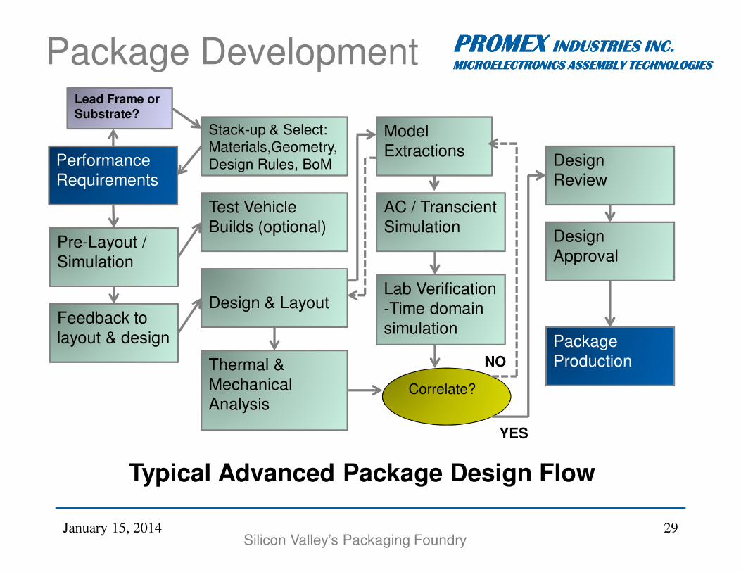
Typical Advanced Package Design Flow
Package Development PROMEX PROMEX PROMEX PROMEX INDUSTRIES INC.INDUSTRIES INC.INDUSTRIES INC.INDUSTRIES INC.
MICROELECTRONICS ASSEMBLY TECHNOLOGIESMICROELECTRONICS ASSEMBLY TECHNOLOGIESMICROELECTRONICS ASSEMBLY TECHNOLOGIESMICROELECTRONICS ASSEMBLY TECHNOLOGIES
Silicon Valley’s Packaging Foundry
Performance
Requirements
Pre-Layout /
Simulation
Feedback to
layout & design
Stack-up & Select:
Materials,Geometry,
Design Rules, BoM
Test Vehicle
Builds (optional)
Design & Layout
Thermal &
Mechanical
Analysis
Model
Extractions
AC / Transcient
Simulation
Lab Verification
-Time domain
simulation
Design
Review
Design
Approval
Package
Production
Correlate?
YES
NO
Lead Frame orSubstrate?
January 15, 2014 29
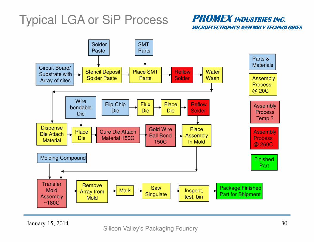
� � � � � �� � � � � �� � � � � �� � � � � �� � � � �� � � ��� � � � �� � � ��� � � � �� � � ��� � � � �� � � ��� � � � � � � � � � � � � � � � � � � � � � � � � � � � � � � � � � � �� � � � � � � � � � � � � � � � � � � � � � � � � � � � � � � � � � � �� � � � � � � � � � � � � � � � � � � � � � � � � � � � � � � � � � � �� � � � � � � � � � � � � � � � � � � � � � � � � � � � � � � � � � � �Typical LGA or SiP Process
Silicon Valley’s Packaging FoundryJanuary 15, 2014 30
Circuit Board/
Substrate with
Array of sites
Solder
Paste
Reflow
Solder
Place SMT
Parts
Stencil Deposit
Solder Paste
Water
Wash
SMT
Parts
Molding Compound
Transfer
Mold
Assembly
~180C
Remove
Array from
Mold
Saw
SingulateMark
Package Finished
Part for Shipment
Parts &
Materials
Assembly
Process
@ 20C
Assembly
Process
Temp ?
Finished
Part
Assembly
Process
@ 260C
Place
Die
Cure Die Attach
Material 150C
Dispense
Die Attach
Material
Place
Assembly
In Mold
Gold Wire
Ball Bond
150C
Wire
bondable
Die
Flip Chip
Die
Flux
Die
Place
Die
Reflow
Solder
Inspect,
test, bin
� � � � � �� � � � � �� � � � � �� � � � � �� � � � �� � � ��� � � � �� � � ��� � � � �� � � ��� � � � �� � � ��� � � � � � � � � � � � � � � � � � � � � � � � � � � � � � � � � � � �� � � � � � � � � � � � � � � � � � � � � � � � � � � � � � � � � � � �� � � � � � � � � � � � � � � � � � � � � � � � � � � � � � � � � � � �� � � � � � � � � � � � � � � � � � � � � � � � � � � � � � � � � � � �
Harvey’s IssueA BTC Assembly Issue: solder voids
January 15, 2014 31
� � � � � �� � � � � �� � � � � �� � � � � �� � � � �� � � ��� � � � �� � � ��� � � � �� � � ��� � � � �� � � ��� � � � � � � � � � � � � � � � � � � � � � � � � � � � � � � � � � � �� � � � � � � � � � � � � � � � � � � � � � � � � � � � � � � � � � � �� � � � � � � � � � � � � � � � � � � � � � � � � � � � � � � � � � � �� � � � � � � � � � � � � � � � � � � � � � � � � � � � � � � � � � � �Harvey’s Issue
Silicon Valley’s Packaging FoundryJanuary 15, 2014 32
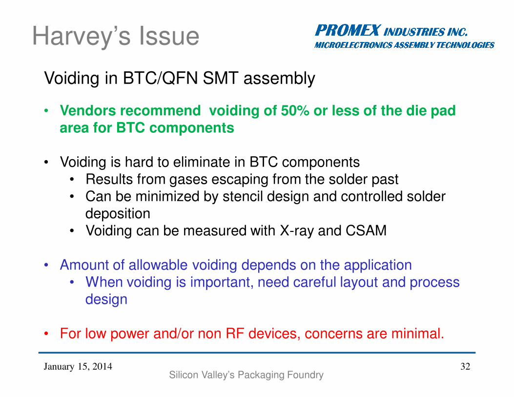
Voiding in BTC/QFN SMT assembly
• Vendors recommend voiding of 50% or less of the die pad area for BTC components
• Voiding is hard to eliminate in BTC components• Results from gases escaping from the solder past• Can be minimized by stencil design and controlled solder
deposition• Voiding can be measured with X-ray and CSAM
• Amount of allowable voiding depends on the application• When voiding is important, need careful layout and process
design
• For low power and/or non RF devices, concerns are minimal.
Conclusions PROMEX PROMEX PROMEX PROMEX INDUSTRIES INC.INDUSTRIES INC.INDUSTRIES INC.INDUSTRIES INC.
MICROELECTRONICS ASSEMBLY TECHNOLOGIESMICROELECTRONICS ASSEMBLY TECHNOLOGIESMICROELECTRONICS ASSEMBLY TECHNOLOGIESMICROELECTRONICS ASSEMBLY TECHNOLOGIES
Silicon Valley’s Packaging Foundry
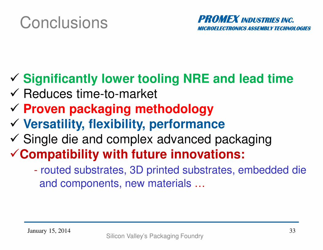
� Significantly lower tooling NRE and lead time� Reduces time-to-market
� Proven packaging methodology� Versatility, flexibility, performance� Single die and complex advanced packaging
�Compatibility with future innovations:- routed substrates, 3D printed substrates, embedded die
and components, new materials …
January 15, 2014 33
Discussion, Questions
PROMEX PROMEX PROMEX PROMEX INDUSTRIES INC.INDUSTRIES INC.INDUSTRIES INC.INDUSTRIES INC.
MICROELECTRONICS ASSEMBLY TECHNOLOGIESMICROELECTRONICS ASSEMBLY TECHNOLOGIESMICROELECTRONICS ASSEMBLY TECHNOLOGIESMICROELECTRONICS ASSEMBLY TECHNOLOGIES
Silicon Valley’s Packaging FoundryJanuary 15, 2014 34