Embed Size (px)
Citation preview
The Pennsylvania State University
The Graduate School
College of Engineering
PROPAGATION AND EXCITATION OF MULTIPLE
SURFACE WAVES
A Dissertation in
Engineering Science and Mechanics
by
Muhammad Faryad
c⃝ 2012 Muhammad Faryad
Submitted in Partial Fulfillment
of the Requirements
for the Degree of
Doctor of Philosophy
May 2012

The dissertation of Muhammad Faryad was reviewed and approved∗ by the fol-lowing:
Akhlesh LakhtakiaCharles Godfrey Binder Professor of Engineering Science and MechanicsDissertation AdviserChair of Committee
Michael T. LanaganProfessor of Engineering Science and MechanicsAssociate Director Materials Research Institute
Osama O. AwadelkarimProfessor of Engineering Science and Mechanics
Jainendra K. JainErwin W. Mueller Professor of Physics
Judith A. ToddP. B. Breneman Professor of Engineering Science and MechanicsHead of the Department of Engineering Science and Mechanics
∗Signatures are on file in the Graduate School.
ii
Abstract
Surface waves are the solutions of the frequency-domain Maxwell equations at theplanar interface of two dissimilar materials. The time-averaged Poynting vectorof a surface wave (i) has a significant component parallel to the interface and (ii)decays at sufficiently large distances normal to the interface. If one of the part-nering materials is a metal and the other a dielectric, the surface waves are calledsurface plasmon-polariton (SPP) waves. If both partnering materials are dielec-tric, with at least one being periodically nonhomogeneous normal to the interface,the surface waves are called Tamm waves; and if that dielectric material is alsoanisotropic, the surface waves are called Dyakonov–Tamm waves. SPP waves alsodecays along the direction of propagation, whereas Tamm and Dyakonov–Tammwaves propagate with negligible losses.
The propagation and excitation of multiple SPP waves guided by the inter-face of a metal with a periodically nonhomogeneous sculptured nematic thinfilm (SNTF), and the interface of a metal with a rugate filter were theoreticallyinvestigated. The SNTF is an anisotropic material with a permittivity dyadicthat is periodically nonhomogeneous in the thickness direction. A rugate filter isalso a periodically nonhomogeneous dielectric material; however, it is an isotropicmaterial.
Multiple SPP waves of the same frequency but with different polarizationstates, phase speeds, attenuation rates, and spatial field profiles were found tobe guided by a metal/SNTF interface, a metal/rugate-filter interface, and a metalslab in the SNTF. Multiple Dyakonov–Tamm waves of the same frequency butdifferent polarization states, phase speeds, and spatial field profiles were found tobe guided by a structural defect in an SNTF, and by a dielectric slab in an SNTF.The characteristics of multiple SPP and Dyakonov–Tamm waves were establishedby the investigations on canonical boundary-value problems.
The Turbadar-Kretschmann-Raether (TKR) and the grating-coupled config-urations were used to study the excitation of multiple SPP waves. In the TKRconfiguration, which is easy to implement in a laboratory, a plane wave of either ofthe two linear polarization states was made incident on the metal-capped rugatefilter of finite thickness and the absorptances were calculated using a numericallystable algorithm. In the grating-coupled configuration, which is required for solarcell applications, a plane wave of either polarization state was made incident on
iii

a rugate filter or an SNTF backed by a finitely thick metallic surface-relief grat-ing and the total absorptance of the structure was calculated using the rigorouscoupled-wave approach. In both the configurations, the excitation of SPP waveswas inferred by the presence of those peaks in the absorptance curves that wereindependent of the thickness of the dielectric material.
It was found that (i) it is the periodic nonhomogeneity (not the anisotropy)of a partnering dielectric material normal to the interface that is responsible forthe multiplicity of surface waves; (ii) multiple SPP, Tamm, Dyakonov–Tamm, andFano waves of the same frequency and different phase speeds and spatial profilescan be guided by an interface of two different materials provided that at leastone of them is periodically nonhomogeneous normal to the interface; (iii) themorphology of the partnering dielectric material affects the number, the phasespeeds, the spatial profiles, and the degrees of localization of the surface waves;(iv) the number of surface waves can be increased further by the coupling of twointerfaces separated by a sufficiently thin layer; and (v) multiple surface wavescan be excited in the TKR and the grating-coupled configurations both with theisotropic and anisotropic but periodically nonhomogeneous dielectric materials.
iv
Nontechnical Abstract
The type of electromagnetic waves that propagate along the interface of two dis-similar materials are called surface waves. These waves are important for manyapplications because most of their energy is localized close to the interface, andthe characteristics of these waves depend heavily on the properties of the part-nering materials close to the interface. The localization of the energy of surfacewaves close to the interface can be used in sensing applications and harvestingsolar energy. In sensing applications, an unknown chemical infiltrates one of thepartnering materials, thereby changing the characteristics of propagating surfacewaves. This change in the characteristics of surface waves can be used to sense theproperties of infiltrating chemical. In thin-film solar cells, the excitation of surfacewaves can increase the absorption of solar energy because a part of the energy ofthe light that is incident on the solar cell can be be used to launch surface wavesinstead of being wasted by reflection.
If one of the two dissimilar materials is a metal and the other a dielectric ma-terial the surface waves are called surface plasmon-polariton (SPP) waves. Amongvarious types of surface waves, SPP waves are the most extensively studied be-cause it is easy to excite and use them in many optical applications, especiallysensing. However, SPP waves can propagate only for short distances along theinterface before their energy is converted to thermal energy. Moreover, for a givencolor (wavelength) of the incident light, only one SPP wave can be excited if boththe partnering materials are homogeneous. Other types of surface waves includeFano waves, Tamm waves and Dyakonov–Tamm waves that propagate guided bythe interface of two dielectric materials. These waves can propagate much longerdistances along the interface than SPP waves; however, it is much more difficultto excite them than SPP waves.
The purpose of this thesis was to theoretically investigate the propagation andexcitation of multiple surface waves of the same color but different polarizationstates, phase speeds, and spatial profiles. It was found that more than one sur-face wave of the same color can be guided by the interface of two materials ifthe partnering dielectric material is made to have periodically changing dielectricproperties along a direction normal to the interface. This holds true for SPP waves,Tamm waves, Dyakonov–Tamm waves, and Fano waves. Multiple SPP waves areguided by the interface of a metal and a periodically nonhomogeneous sculptured
v
nematic thin film (SNTF) and the interface of the metal and a rugate filter. Boththe SNTF and the rugate filter are periodically nonhomogeneous dielectric mate-rials; however, an SNTF is an anisotropic and porous material, whereas a rugatefilter is an isotropic material. The porosity of the SNTF can be used in sensingapplications and the isotropy of the rugate filter makes possible the applicationof multiple SPP waves in solar cells because rugate filters can be fabricated withsemiconductor materials. The number of multiple surface waves can be increasedfurther if two interfaces are placed in close proximity. The coupling of the twointerfaces leads to the emergence of new surface waves that are not guided byeither interface independently.
Since surface waves propagate with a different phase speed than the waves inthe bulk of either of the partnering materials, the excitation of the surface wavesrequires a technique to match the phase speed of the incident light to that of thepossible surface wave. For this purpose, attenuated total reflection (ATR) andscattering by a surface-relief grating, among others, are used. In this thesis, it isshown that multiple SPP waves can also be excited using both the ATR and thesurface-relief gratings for metal/SNTF and metal/rugate-filter interfaces.
Availability of multiple surface waves, all of the same color, offers excitingpossibilities in applications. For sensing applications, more than one surface wavescan be used to detect more than one chemicals at the same time. For solar energyharvesting, the availability of multiple SPP waves can increase the absorption oflight as compared to the case when only one SPP wave can be excited.
vi
Contents
List of Acronyms xi
List of Symbols xii
List of Figures xv
List of Tables xxvii
Acknowledgments xxx
1 Introduction 11.1 Surface Plasmon-Polariton Waves . . . . . . . . . . . . . . . . . . . 31.2 Dyakonov–Tamm Waves . . . . . . . . . . . . . . . . . . . . . . . . 41.3 Sculptured Nematic Thin Films . . . . . . . . . . . . . . . . . . . . 51.4 Rugate Filters . . . . . . . . . . . . . . . . . . . . . . . . . . . . . . 61.5 Excitation of Surface Waves . . . . . . . . . . . . . . . . . . . . . . 7
1.5.1 Prism-Coupled Configuration . . . . . . . . . . . . . . . . . 71.5.2 Grating-Coupled Configuration . . . . . . . . . . . . . . . . 91.5.3 Waveguide-Coupled Configuration . . . . . . . . . . . . . . . 10
1.6 Objectives of the Thesis . . . . . . . . . . . . . . . . . . . . . . . . 101.7 Organization of the Thesis . . . . . . . . . . . . . . . . . . . . . . . 11
2 SPP Waves Guided by Metal/SNTF Interface 142.1 Introduction . . . . . . . . . . . . . . . . . . . . . . . . . . . . . . . 142.2 Theory . . . . . . . . . . . . . . . . . . . . . . . . . . . . . . . . . . 152.3 Numerical Results and Discussion . . . . . . . . . . . . . . . . . . . 17
2.3.1 ψ = 0 . . . . . . . . . . . . . . . . . . . . . . . . . . . . . . 202.3.2 ψ = 75 . . . . . . . . . . . . . . . . . . . . . . . . . . . . . 21
2.4 Concluding Remarks . . . . . . . . . . . . . . . . . . . . . . . . . . 23
3 SPP Waves Guided by Metal/Rugate-Filter Interface 243.1 Introduction . . . . . . . . . . . . . . . . . . . . . . . . . . . . . . . 243.2 Theory . . . . . . . . . . . . . . . . . . . . . . . . . . . . . . . . . . 25
vii

3.3 Numerical Results and Discussion . . . . . . . . . . . . . . . . . . . 273.4 Concluding Remarks . . . . . . . . . . . . . . . . . . . . . . . . . . 32
4 Propagation of Multiple Fano Waves 334.1 Introduction . . . . . . . . . . . . . . . . . . . . . . . . . . . . . . . 334.2 Numerical Results and Discussion . . . . . . . . . . . . . . . . . . . 344.3 Concluding Remarks . . . . . . . . . . . . . . . . . . . . . . . . . . 38
5 Dyakonov–Tamm Waves Guided by a Phase-Twist Defect in anSNTF 395.1 Introduction . . . . . . . . . . . . . . . . . . . . . . . . . . . . . . . 395.2 Theory . . . . . . . . . . . . . . . . . . . . . . . . . . . . . . . . . . 405.3 Numerical Results and Discussion . . . . . . . . . . . . . . . . . . . 43
5.3.1 Multiple solutions of dispersion equation . . . . . . . . . . . 455.3.2 Decay constants . . . . . . . . . . . . . . . . . . . . . . . . . 455.3.3 Spatial profiles . . . . . . . . . . . . . . . . . . . . . . . . . 48
5.4 Concluding Remarks . . . . . . . . . . . . . . . . . . . . . . . . . . 50
6 SPP Waves Guided by a Metal Slab in an SNTF 526.1 Introduction . . . . . . . . . . . . . . . . . . . . . . . . . . . . . . . 526.2 Canonical Boundary-Value Problem . . . . . . . . . . . . . . . . . . 536.3 Numerical Results and Discussion . . . . . . . . . . . . . . . . . . . 57
6.3.1 Bulk aluminum defect layer . . . . . . . . . . . . . . . . . . 576.3.2 Electron-beam evaporated aluminum thin film . . . . . . . . 66
6.4 Concluding Remarks . . . . . . . . . . . . . . . . . . . . . . . . . . 71
7 Guided-Wave Propagation by a Dielectric Slab in an SNTF 727.1 Introduction . . . . . . . . . . . . . . . . . . . . . . . . . . . . . . . 727.2 Numerical Results and Discussion . . . . . . . . . . . . . . . . . . . 73
7.2.1 Dyakonov–Tamm waves guided by a single dielectric/SNTFinterface . . . . . . . . . . . . . . . . . . . . . . . . . . . . . 73
7.2.2 SNTF/dielectric/SNTF system . . . . . . . . . . . . . . . . 747.2.3 Comparison with SNTF/metal/SNTF system of Ch. 6 . . . 81
7.3 Concluding Remarks . . . . . . . . . . . . . . . . . . . . . . . . . . 82
8 Prism-Coupled Excitation of Multiple SPP Waves 848.1 Introduction . . . . . . . . . . . . . . . . . . . . . . . . . . . . . . . 848.2 Theoretical Formulations . . . . . . . . . . . . . . . . . . . . . . . . 85
8.2.1 TKR configuration . . . . . . . . . . . . . . . . . . . . . . . 858.2.2 Canonical-boundary value problem for coupled-SPP-wave
propagation . . . . . . . . . . . . . . . . . . . . . . . . . . . 908.3 Numerical Results and Discussion . . . . . . . . . . . . . . . . . . . 92
8.3.1 p-polarization state . . . . . . . . . . . . . . . . . . . . . . . 93
viii
8.3.2 s-polarization state . . . . . . . . . . . . . . . . . . . . . . . 988.4 Concluding Remarks . . . . . . . . . . . . . . . . . . . . . . . . . . 102
9 Grating-Coupled Excitation of Multiple SPP Waves Guided byMetal/Rugate-Filter Interface 1049.1 Introduction . . . . . . . . . . . . . . . . . . . . . . . . . . . . . . . 1049.2 Boundary-Value Problem . . . . . . . . . . . . . . . . . . . . . . . . 105
9.2.1 Description . . . . . . . . . . . . . . . . . . . . . . . . . . . 1059.2.2 Coupled ordinary differential equations . . . . . . . . . . . . 1069.2.3 Solution algorithm . . . . . . . . . . . . . . . . . . . . . . . 109
9.3 Numerical Results and Discussion . . . . . . . . . . . . . . . . . . . 1119.3.1 Homogeneous dielectric partnering material . . . . . . . . . 1119.3.2 Periodically nonhomogeneous dielectric partnering material . 115
9.4 Concluding Remarks . . . . . . . . . . . . . . . . . . . . . . . . . . 126
10 Enhanced Absorption of Light Due to Multiple SPP Waves 12810.1 Introduction . . . . . . . . . . . . . . . . . . . . . . . . . . . . . . . 12810.2 Numerical Results and Discussion . . . . . . . . . . . . . . . . . . . 129
10.2.1 Homogeneous semiconductor partnering material . . . . . . 12910.2.2 Periodically nonhomogeneous semiconductor partnering ma-
terial . . . . . . . . . . . . . . . . . . . . . . . . . . . . . . . 13110.3 Concluding Remarks . . . . . . . . . . . . . . . . . . . . . . . . . . 137
11 Grating-Coupled Excitation of Multiple SPP Waves Guided byMetal/SNTF Interface 13911.1 Introduction . . . . . . . . . . . . . . . . . . . . . . . . . . . . . . . 13911.2 Boundary-Value Problem . . . . . . . . . . . . . . . . . . . . . . . . 140
11.2.1 Description . . . . . . . . . . . . . . . . . . . . . . . . . . . 14011.2.2 Coupled ordinary differential equations . . . . . . . . . . . . 14211.2.3 Solution algorithm . . . . . . . . . . . . . . . . . . . . . . . 14611.2.4 Absorptance . . . . . . . . . . . . . . . . . . . . . . . . . . . 148
11.3 Numerical Results and Discussion . . . . . . . . . . . . . . . . . . . 14911.3.1 γ− = 0 . . . . . . . . . . . . . . . . . . . . . . . . . . . . . 15011.3.2 γ− = 75 . . . . . . . . . . . . . . . . . . . . . . . . . . . . . 15611.3.3 Comparison with the TKR configuration . . . . . . . . . . . 160
11.4 Concluding Remarks . . . . . . . . . . . . . . . . . . . . . . . . . . 162
12 Conclusions and Suggestions for Future Work 16412.1 Conclusions . . . . . . . . . . . . . . . . . . . . . . . . . . . . . . . 16412.2 Suggestions for Future Work . . . . . . . . . . . . . . . . . . . . . . 169
12.2.1 Excitation of multiple surface waves with a finite source . . . 16912.2.2 Simultaneous excitation of all possible SPP waves using quasi-
periodic surface-relief grating . . . . . . . . . . . . . . . . . 169
ix

12.2.3 Excitation of Tamm and Dyakonov–Tamm waves . . . . . . 17012.2.4 Thin-film solar cell with actual configuration . . . . . . . . . 170
A Propagation of Multiple Tamm Waves 171A.1 Introduction . . . . . . . . . . . . . . . . . . . . . . . . . . . . . . . 171A.2 Theory . . . . . . . . . . . . . . . . . . . . . . . . . . . . . . . . . . 172
A.2.1 s-polarized surface waves . . . . . . . . . . . . . . . . . . . . 172A.2.2 p-polarized surface waves . . . . . . . . . . . . . . . . . . . . 173
A.3 Numerical Results and Discussion . . . . . . . . . . . . . . . . . . . 174A.3.1 Homogeneous-dielectric/rugate-filter interface . . . . . . . . 174A.3.2 Rugate filter with a phase defect . . . . . . . . . . . . . . . 177A.3.3 Rugate filter with sudden change of mean refractive index . 182A.3.4 Rugate filter with sudden change of amplitude . . . . . . . . 183A.3.5 Interface of two distinct rugate filters . . . . . . . . . . . . . 184
A.4 Concluding Remarks . . . . . . . . . . . . . . . . . . . . . . . . . . 186
B MathematicaTM Codes 188B.1 Newton-Raphson Method to Find κ in the Canonical Boundary-
Value Problem of Ch. 2 . . . . . . . . . . . . . . . . . . . . . . . . . 188B.2 Plotting the Components of P of a p-Polarized SPP Wave in the
Canonical Boundary-Value Problem of Ch. 2 . . . . . . . . . . . . . 191B.3 Newton-Raphson Method to Find κ in the Canonical Boundary-
Value Problem of Ch. 5 . . . . . . . . . . . . . . . . . . . . . . . . . 196B.4 Newton-Raphson Method to Find κ in the Canonical Boundary-
Value Problem of Chs. 6 and 7 . . . . . . . . . . . . . . . . . . . . . 200B.5 Ap vs. θ in the TKR Configuration of Ch. 8 . . . . . . . . . . . . . 203B.6 Ap vs. θ in the Grating-Coupled Configuration of Chs. 9 and 10 . . 206B.7 Ap and As vs. θ in the Grating-Coupled Configuration of Ch. 11 . . 212
Bibliography 223
x

List of Acronyms
ATR attenuated total reflection
CTF columnar thin film
CSTF chiral sculptured thin film
deg degrees
Im imaginary part
PV photovoltaic
PVD physical vapor deposition
RCWA rigorous coupled-wave approach
Re real part
SNTF sculptured nematic thin film
SPP surface plasmon-polariton
STF sculptured thin film
TKR Turbadar-Kretschmann-Raether
TO Turbadar-Otto
xi
List of Symbols
A planewave absorptance
ap, as scalar amplitudes representing p- and s-polarized waves
Ap, As absorptances for p- and s-polarized incidence
αmet wavenumber of SPP wave in the metal normalto the direction of propagation
αn nth eigenvalue corresponding to nth eigenvector [t](n)
of 4× 4 matrix [Q]
α±n nth eigenvalue corresponding to nth eigenvector [t±](n)
of 4× 4 matrix [Q±]
d1 thickness of the dielectric layer in the grating-coupled configuration
d2 combined thickness of the dielectric layer and the grating depth(d2 = d1 + Lg)
d3 total thickness of the structure in the grating-coupled configuration(d3 = d2 + Lm)
∆ e-folding distance into the dielectric material
∆met skin depth of the metal
∆±n amplitude of refractive-index modulation of rugate filter for z ≷ 0
e auxiliary electric field phasor
E electric field phasor
exp(−u1,2) decay constants of Dyakonov–Tamm wave when z → ∞exp(−v1,2) decay constants of Dyakonov–Tamm wave when z → −∞ϵ0 permittivity of free space
ϵa, ϵb, ϵc relative permittivity scalars
ϵℓ relative permittivity of the prism material in the TKR configuration
ϵr, ϵd relative permittivity of dielectric material
xii

ϵm relative permittivity of metal
ϵ(n) nth coefficient of Fourier series of permittivity ϵ(x)
ϵSNTF
permittivity dyadic of the SNTF
η0 intrinsic impedance of free space
[f ] column vector containing x- and y-components of e and h
γ fraction of the amplitude of sinusoidal variationin refractive index of a rugate filter
γ± the angle between the morphologically significant plane ofan SNTF and the x-axis in the region z ≷ 0
h auxiliary magnetic field phasor
H magnetic field phasor
kmet wavevector of the SPP wave in the metal
k(n)x x-component of nth Floquet harmonic
κ wavenumber of a surface wave in the canonical problemalong the direction of propagation
k0 wavenumber in free space
L period of surface-relief grating
L1 width of the bump in the surface-relief grating
Lg depth of the surface-relief grating
Lm thickness of the metal film in the TKR and grating-coupledconfigurations
Lmet thickness of the metal slab in the canonical problem
Ls thickness of dielectric slab
λ0 wavelength in free space
na lowest value of refractive index in a rugate filter
nb highest value of refractive index in a rugate filter
n±avg mean refractive index of rugate filter for z ≷ 0
nℓ refractive index of the prism material in the TKR configuration
Nd number of slices in the dielectric material
Ng number of slices in the grating region
Np number of period of the rugate filter in the TKR configuration
±Nt ending and starting indexes in summations in RCWA
xiii
[P ] coefficient matrix of matrix ordinary differential equation
[P±] matrix [P ] in the region z ≷ 0
P time-averaged Poynting vector
P1 the component of P along the direction ofpropagation of an SPP wave
P2 the component of P in the interface plane andnormal to the direction of propagation of an SPP wave
Px,y,z x-, y- and z-components of P
[Q] optical response of one period of an SNTF
[Q±] matrix [Q] in the region z ≷ 0
[Q] auxiliary matrix defined by [Q] = expi2Ω[Q]rp, rs reflection amplitudes of p- and s-polarized waves
ψ angle between the direction of propagation of a surface wave andthe morphologically significant plane of an SNTF
tp, ts transmission amplitudes of p- and s-polarized waves
ux, uy, uy unit vectors along x-, y- and z- axis
µ0 permeability of free space
θ incidence angle with the z-axis
ϕ incidence angle with the x-axis in the xy plane
ϕ± phase shift in the SNTF or rugate filter in the region z ≷ 0
ω angular frequency
Ω half-period of an SNTF or a rugate filter
Ω± half-period of an SNTF or a rugate filter in the region z ≷ 0
χv vapor incidence angle
δv amplitude of periodic variation of incident vapor
χv the tilt of columns in an STF
xiv
List of Figures
1.1 Schematic for the TKR configuration. . . . . . . . . . . . . . . . . . 81.2 Schematic for the TO configuration. . . . . . . . . . . . . . . . . . . 81.3 Schematic for the grating-coupled configuration. . . . . . . . . . . . 91.4 Schematic for the waveguide-coupled configuration. . . . . . . . . . 101.5 A flow diagram showing the interconnections among different chap-
ters of this thesis. The boxes with blue light background repre-sent the chapters containing the canonical boundary-value prob-lems, and the boxes with purple dark background represent thechapters that contain the boundary-value problems for the excita-tion of multiple surface waves. The boxes with white backgrounddo not contain any of the boundary-value problems. . . . . . . . . . 12
2.1 (left) Real and (right) imaginary parts of κ as functions of ψ, forSPP-wave propagation guided by the planar interface of aluminumand a titanium-oxide SNTF. Either two or three modes are possible,depending on ψ. . . . . . . . . . . . . . . . . . . . . . . . . . . . . . 18
2.2 Variations of components of e (in V m−1), h (in A m−1), and P(in W m−2) with z along the line x = 0, y = 0, for κ = (2.455 +i0.04208)k0 and ψ = 0. The components parallel to u1, u2, anduz, are represented by black solid, red dashed, and blue chain-dashed lines, respectively. The data were computed by settingap = 1 V m−1, with as = 0, b1 = 0, and b2 = −1.3026 − i7.9841then obtained using (2.15). . . . . . . . . . . . . . . . . . . . . . . 18
2.3 Same as Fig. 2.2 except for κ = (2.080 + i0.003538)k0. The datawere computed by setting as = 1 V m−1, with ap = 0, b1 = −1, andb2 = 0 then obtained using (2.15). Theoretical analysis confirmsthat u1 ·P > 0 for z < 0 for this case. . . . . . . . . . . . . . . . . 19
2.4 Same as Fig. 2.2 except for κ = (1.868 + i0.007267)k0. The datawere computed by setting ap = 1 V m−1, with as = 0, b1 = 0, andb2 = −1.3397− i7.8300 then obtained using (2.15). . . . . . . . . . 20
xv
2.5 Same as Fig. 2.2 except for κ = (2.459 + i0.04247)k0 and ψ =75. The data were computed by setting ap = 1 V m−1, withas = 0.1919 − i0.0429 V m−1, b1 = 13.0153 − i5.3299, and b2 =−12.6239 + i2.8422 then obtained using (2.15). . . . . . . . . . . . . 21
2.6 Same as Fig. 2.2 except for κ = (2.066 + i0.003861)k0 and ψ =75. The data were computed by setting ap = 1 V m−1, withas = −15.9578 + i3.4826 V m−1, b1 = −17.8249 − i35.4678, andb2 = 25.4223 + i31.0644 then obtained using (2.15). . . . . . . . . . 22
3.1 (left) Real and (right) imaginary parts of κ/k0 as functions of Ω/λ0
for SPP-wave propagation guided by the planar interface of alu-minum and a rugate filter described by Eq. (3.1) with na = 1.45and nb = 2.32. . . . . . . . . . . . . . . . . . . . . . . . . . . . . . . 28
3.2 Variations with z of the Cartesian components of e (in V m−1), h(in A m−1), and P (in W m−2) along the line x = 0, y = 0. Thecomponents parallel to ux, uy, and uz, are represented by red solid,blue dashed, and black chain-dashed lines, respectively. The datawere computed by setting ap = 1 V m−1. (left) Ω/λ0 = 0.1, κ/k0 =2.00943+0.04468i, and (right) Ω/λ0 = 1, κ/k0 = 2.21456+0.00246i.Both solutions lie on the branch labeled p8 in Fig. 3.1. . . . . . . . 29
3.3 Same as Fig. 3.2 except for (left) Ω/λ0 = 1, κ/k0 = 1.4864 +0.0013203i, and (right) Ω/λ0 = 1.5, κ/k0 = 1.7873 + 0.0007801i,and the data were computed by setting as = 1 V m−1. Both solu-tions lie on the branch labeled s2 in Fig. 3.1. . . . . . . . . . . . . 30
3.4 (left) Real and (right) imaginary parts of κ/k0 as functions γ ∈[1, 0.001] with Ω = 2λ0 for SPP-wave propagation guided by the pla-nar interface of aluminum and a rugate filter described by Eq. (3.17)with na = 1.45, nb = 2.32, and Ω = 2λ0. . . . . . . . . . . . . . . . 31
3.5 Same as Fig. 3.2 except for (left) γ = 0.5 and κ/k0 = 1.78142 +0.00288i on the branch labeled p3 in Fig. 3.4, and (right) γ = 0.1and κ/k0 = 1.9515 + 0.01943i on on the branch labeled p10 inFig. 3.4. . . . . . . . . . . . . . . . . . . . . . . . . . . . . . . . . . 32
4.1 Variation of relative permittivity along the z axis for na = 1.45,nb = 2.32, and ϵm = −2. Although the semi-infinite rugate filterdepicted here is a continuously nonhomogeneous medium, it canalso be piecewise homogeneous. . . . . . . . . . . . . . . . . . . . . 35
4.2 Relative wavenuber κ/k0 versus ϵm ∈ [−6, 0] for Fano-wave prop-agation when Ω = λ0 = 633 nm, na = 1.45, and nb = 2.32. Thered circles represent s-polarized, while the black triangles representp-polarized, Fano waves. The gap in one of the solution branchesappears to be a numerical artifact. . . . . . . . . . . . . . . . . . . 35
xvi
4.3 Variations of the magnitudes of the Cartesian components of electricand magnetic field phasors (in V m−1 and A m−1, respectively)with z. The x-, y-, and z-directed components are represented bysolid red, blue dashed, and black chain-dashed lines, respectivelyfor ϵm = −6. Left: κ/k0 = 3.1283 and p-polarization state. Right:κ/k0 = 1.9885 and s-polarization state. . . . . . . . . . . . . . . . . 36
4.4 Same as Fig. 4.3 except for ϵm = 0. Left: κ/k0 = 1.7145 andp-polarization state. Right: κ/k0 = 1.5161 and s-polarization state. 37
4.5 Same as Fig. 4.2, except that ϵm ∈ [0, 2]. The waves represented bythese solutions have to be classified as Tamm waves [16]. . . . . . . 37
5.1 Schematic illustration of the geometry of the problem, when γ+ = γ−. 415.2 The solutions κ/k0 of the dispersion equation (5.18) as functions of
γ+ for certain specific values of γ−. (a) First, (b) second, (c) third,and (d) fourth sets of solutions. . . . . . . . . . . . . . . . . . . . . 44
5.3 The decay constants exp(−u1), exp(−u2), exp(−v1), and exp(−v2)for the (a) first, (b) second, (c) third, and (d) fourth set of solutionsin Fig. 5.2. . . . . . . . . . . . . . . . . . . . . . . . . . . . . . . . . 46
5.4 Variations with z of the magnitudes of the Cartesian componentsof E (in V m−1), H (in A m−1), and P (in W m−2), when γ− = 60,γ+ = 30, and κ/k0 = 1.3522. The components parallel to ux,uy, and uz, are represented by red solid, blue dashed, and blackchain-dashed lines, respectively. . . . . . . . . . . . . . . . . . . . . 47
5.5 Same as Fig. 5.4 except that κ/k0 = 2.02646. . . . . . . . . . . . . . 485.6 Same as Fig. 5.4 except that κ/k0 = 2.2395. . . . . . . . . . . . . . 495.7 Same as Fig. 5.4 except that κ/k0 = 2.3050. . . . . . . . . . . . . . 50
6.1 Schematic illustration of the geometry of the canonical boundary-value problem for γ+ = γ−. . . . . . . . . . . . . . . . . . . . . . . 54
6.2 Variation of real and imaginary parts of κ/k0 with γ+, when γ− =
γ+. (a) L± = ±7.5 nm, (b) L± = ±12.5 nm, (c) L± = ±25 nm,and (d) L± = ±45 nm. . . . . . . . . . . . . . . . . . . . . . . . . . 58
6.3 Variation of the Cartesian components of the time-averaged Poynt-ing vector P(x, z) (in W m−2) along the z axis when x = 0, L± =±7.5 nm, and γ− = γ+. (a-c) γ+ = 0, and (d-f) γ+ = 25.(a) κ/k0 = 2.6387 + i0.1839, (b) κ/k0 = 2.0964 + i0.009997, (c)κ/k0 = 1.9048 + i0.02696, (d) κ/k0 = 2.6399 + i0.1848, (e) κ/k0 =2.09285 + i0.00988, and (f) κ/k0 = 1.9103 + i0.02405. The x-, y-and z-directed components of P(x, z) are represented by solid red,dashed blue, and chain-dashed black lines, respectively. . . . . . . 59
xvii
6.4 Same as Fig. 6.3 except for L± = ±45 nm. (a) κ/k0 = 2.4549 +i0.04173, (b) κ/k0 = 2.08034 + i0.003574, (c) κ/k0 = 1.8683 +i0.00734, (d) κ/k0 = 2.4557+i0.04181, (e) κ/k0 = 2.0773+i0.00363,and (f) κ/k0 = 1.8830 + i0.00413. . . . . . . . . . . . . . . . . . . . 60
6.5 Same as Fig. 6.2 except that γ− = γ+ + 90. . . . . . . . . . . . . 626.6 Variation of the Cartesian components of the time-averaged Poynt-
ing vector P(x, z) (in W m−2) along the z axis when x = 0, L± =±7.5 nm, and γ− = γ+ + 90. (a-c) γ+ = 0, and (d-f) γ+ =25. The following values of κ were chosen for rough correspon-dence with those in Fig. 6.3: (a) κ/k0 = 2.3753 + i0.005699, (b)κ/k0 = 2.09013 + i0.009135, (c) κ/k0 = 1.9133 + i0.004397, (d)κ/k0 = 2.3756 + i0.005713, (e) κ/k0 = 2.08797 + i0.009324, and (f)κ/k0 = 1.9165 + i0.01117. . . . . . . . . . . . . . . . . . . . . . . . 63
6.7 Variation of the Cartesian components of the time-averaged Poynt-ing vector P(x, z) (in W m−2) along the z axis when x = 0, L± =±45 nm, and γ− = γ+ + 90. The following values of κ andγ+ were chosen to highlight the uncoupling of the two metal/S-NTF interfaces, when the metal slab is sufficiently thick. (a-e)γ+ = 25 and (f) γ+ = 65. (a) κ/k0 = 2.4558 + i0.04214, (b)κ/k0 = 2.07725 + i0.003595, (c) κ/k0 = 1.8830 + i0.004085, (d)κ/k0 = 2.45833+ i0.0424391, (e) κ/k0 = 2.06775+ i0.00381762, and(f) κ/k0 = 1.8830 + i0.004085. . . . . . . . . . . . . . . . . . . . . 64
6.8 Same as Fig. 6.2 except γ− = γ+ + 45. . . . . . . . . . . . . . . . 656.9 Variation of the Cartesian components of P(x, z) (in W m−2) along
the z axis when x = 0, L± = ±7.5 nm, and γ− = γ+ + 45. (a-c)γ+ = 25, and (d-f) γ+ = 150. (a) κ/k0 = 2.6423 + i0.1865, (b)κ/k0 = 2.08764 + i0.009246, (c) κ/k0 = 1.9159 + i0.009486, (d)κ/k0 = 2.6398 + i0.1847, (e) κ/k0 = 2.09389 + i0.01000, and (f)κ/k0 = 1.9108 + i0.02442. . . . . . . . . . . . . . . . . . . . . . . . 66
6.10 Same as Fig. 6.4 except for γ− = γ+ + 45 . . . . . . . . . . . . . . 676.11 Real and imaginary parts of κ/k0, which represent SPP-wave prop-
agation guided by the single interface of the chosen SNTF andelectron-beam-evaporated aluminum: ϵm = (0.75 + i3.9)2. . . . . . . 67
6.12 Variations of real and imaginary parts of κ/k0 with γ+. (a) L± =±7.5 nm, (b) L± = ±25 nm, (c) L± = ±45 nm, and (d) L± =±75 nm. The other parameters are provided at the beginning ofSec. 6.3.2. . . . . . . . . . . . . . . . . . . . . . . . . . . . . . . . . 68
xviii

6.13 Variation of the Cartesian components of the time-averaged Poynt-ing vector P(x, z) (in W m−2) along the z axis when x = 0, L± =±7.5 nm. (a-c) γ+ = 0, and (d-f) γ+ = 25. The following val-ues of κ were to highlight the coupled SPP-waves propagation:(a) κ/k0 = 2.40502 + i0.015, (b) κ/k0 = 2.06954 + i0.00239, (c)κ/k0 = 1.38082 + i0.00969, (d) κ/k0 = 2.40519 + i0.01502, (e)κ/k0 = 2.07249 + i0.00297, and (f) κ/k0 = 1.38392 + i0.01444.The components parallel to ux, uy, and uz, are represented by redsolid, blue dashed, and black chain-dashed lines, respectively. . . . . 69
6.14 Same as Fig. 6.13 except for L± = ±75 nm, and γ+ = 25. Thefollowing values of κ were chosen to highlight the decoupling of thetwo metal/SNTF interfaces: (a) κ/k0 = 2.78049 + i0.22347, (b)κ/k0 = 2.09306 + i0.00492, (c) κ/k0 = 1.94284 + i0.01149, and (d)κ/k0 = 1.3355 + i0.00534. . . . . . . . . . . . . . . . . . . . . . . . 70
7.1 Relative wavenumber κ/k0, relative phase speed vr, the e-foldingdistance ∆, and the decay constants exp (u1,2) = exp
(2Ω · Im
[α+1,2
])as functions of γ+ for Dyakonov–Tamm waves guided by the singleinterface of the chosen dielectric material and the SNTF. The blacksymbols (square) identify the solutions also found by Agarwal etal. [64], but the solutions identified by the red symbols (circular)were missed in that work. . . . . . . . . . . . . . . . . . . . . . . . 74
7.2 Variation of relative wavenumber κ/k0 with γ+, when γ− = γ+. (a)
L± = ±1 Ω, (b) L± = ±1.5 Ω, (c) L± = ±3 Ω, and (d) L± = ±4 Ω.Solutions in the shaded regions represent Dyakonov–Tamm waves,but those in the unshaded regions represent waveguide modes, theboundary between the two regions being delineated for the chosenparameters by κ/k0 = ns. . . . . . . . . . . . . . . . . . . . . . . . . 75
7.3 Variation of the Cartesian components of P(z) (in W m−2) with zfor γ− = γ+ and L± = ±Ω. The x-, y-, and z-directed componentsare represented by solid red, dashed blue and chain-dashed blacklines. The orange-shaded region represents the dielectric slab. γ+ =(a-d) 10 and (e-f) 80. κ/k0 = (a) 1.85608, (b) 1.83154, (c) 1.82269,(d) 1.59488, (e) 1.77007, and (f) 1.69357. . . . . . . . . . . . . . . . 77
7.4 Same as Fig. 7.3 except for L± = ±4Ω and κ/k0 = (a) 1.84489, (b)1.81941, (c) 1.60496, (d) 1.5111, (e) 1.79381, and (f) 1.70705. . . . . 78
7.5 Same as Fig. 7.2 except for γ− = γ+ + 90. . . . . . . . . . . . . . . 797.6 Same as Fig. 7.3 except for γ− = γ+ + 90. γ+ = (a-c) 10, and
(d-f) 40. κ/k0 = (a) 1.83852, (b) 1.81781, (c) 1.58016, (d) 1.90188,(e) 1.72464, and (f) 1.55786. . . . . . . . . . . . . . . . . . . . . . . 80
xix
7.7 Same as Fig. 7.3 except for γ− = γ+ + 90, and L± = ±4Ω. γ+ =(a-c) 6, (d-e) 30, and (f) 20. κ/k0 = (a) 1.83987, (b) 1.69641, (c)1.66692, (d) 1.87242, (e) 1.66533, and (f) 1.78769. . . . . . . . . . . 80
8.1 Schematic of the TKR configuration. . . . . . . . . . . . . . . . . . 858.2 Schematic of the canonical boundary-value problem for coupled-
SPP-wave propagation due to the metal film. . . . . . . . . . . . . . 908.3 Absorptance Ap as function of the incidence angle θ in the TKR
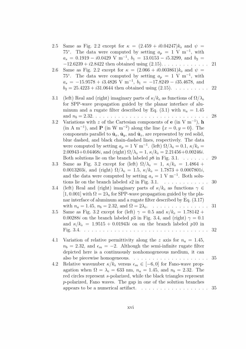
configuration, when λ0 = 633 nm, nℓ = 2.58, Lm = 30 nm, andΩ = 1.5λ0. Solid red line is for Np = 3 and dashed blue line is forNp = 4. Others parameters are given at the beginning of Sec. 8.3. . 93
8.4 Variation of Ap with Lm at the θ-values of the Ap-peaks for Np = 4in the TKR configuration. (a) Green solid line is for θ = 33.23,black dashed line for θ = 37.20, red chain-dashed line for θ =42.41, and blue dotted line is for θ = 48.01; (b) red solid line is forθ = 53.86, black dashed line for θ = 59.66, and blue chain-dashedline is for θ = 61.01. . . . . . . . . . . . . . . . . . . . . . . . . . 94
8.5 Variations of the Cartesian components Px and Pz (in W m−2) ofthe time-averaged Poynting vector along the z axis in (left) themetal film and (right) the rugate filter for Lm = 30 nm in the TKRconfiguration for a p-polarized incident plane wave (ap = 1 V m−1,as = 0). (top) θ = 33.23, (middle) θ = 42.41, and (bottom)θ = 59.66. Red solid line represents Px, blue dashed line representsPz, and Py is identically zero. . . . . . . . . . . . . . . . . . . . . . 96
8.6 Variations of the Cartesian components of the time-averaged Poynt-ing vector P(x = 0, z) (in W m−2) along the z axis in (top) theprism material, (middle) the metal film with Lm = 30 nm, and(bottom) the rugate filter for the canonical boundary-value prob-lem formulated in Sec. 8.2.2 for a p-polarized SPP wave with (left)κ/k0 = 1.4125 + 0.0004i, and (right) κ/k0 = 2.2302 + 0.0173i. Redsolid line represents Px, blue dashed line represents Pz, and Py isidentically zero. The computations were made with bp = 1 V m−1. . 97
8.7 Same as Fig. 8.3 except that As is plotted instead of Ap. . . . . . . 988.8 Variation of As vs. the thickness of the metal film Lm at the θ-
position of the As-peaks for Np = 3 in the TKR configuration.Solid red line is for θ = 38.97, black dashed line for θ = 44.01,blue chain-dashed for θ = 49.22, green dotted line for θ = 54.63,and orange dashed line (with larger dashes) is for θ = 60.66. . . . . 99
xx

8.9 Variations of the Cartesian components Px and Pz (in W m−2) ofthe time-averaged Poynting vector along the z axis in (left) themetal film and (right) the rugate filter for Lm = 30 nm in theTKR configuration for an s-polarized incident plane wave (ap = 0,as = 1 V m−1). (top) θ = 49.22, and (bottom) θ = 60.66. Redsolid line represents Px, blue dashed line represents Pz, and Py isidentically zero. . . . . . . . . . . . . . . . . . . . . . . . . . . . . . 100
8.10 Variations of the Cartesian components of the time-averaged Poynt-ing vector P(x = 0, z) (in W m−2) along the z axis in (top) theprism material, (middle) the metal film with Lm = 30 nm, and(bottom) the rugate filter for two s-polarized SPP waves obtainedfrom the solution of the canonical boundary-value problem shownin Fig. 8.2. (left) κ/k0 = 1.9534 + 0.0004i, and (right) κ/k0 =2.2490 + 1.0136× 10⁻⁵i. Red solid line represents Px, blue dashedline represents Pz, and Py is identically zero. The computationswere made with bs = 1 Vm−1. . . . . . . . . . . . . . . . . . . . . . 101
9.1 Schematic of the boundary-value problem solved using the RCWA. . 1079.2 Absorptance Ap as a function of the incidence angle θ when the
surface-relief grating is defined by either (a) Eq. (9.53) or (b) Eq. (9.2).Black squares represent d1 = 1500 nm, red circles d1 = 1000 nm,and blue triangles d1 = 800 nm. The grating depth (d2 − d1 =50 nm) and the thickness of the metallic layer (d3 − d2 = 30 nm)are the same for all cases. The vertical arrows identify SPP waves. . 113
9.3 Variation of the x-component of the time-averaged Poynting vectorP(x, z) along the z axis in the regions (left) 0 < z < d1 and (right)d1 < z < d3 at x = 0.75L for θ = 12.5, when the surface-reliefgrating is defined by either (a) Eq. (9.53) or (b) Eq. (9.2) and theincident plane wave is p polarized. Other parameters are the sameas for Fig. 9.2. . . . . . . . . . . . . . . . . . . . . . . . . . . . . . . 114
9.4 Absorptances (a) Ap and (b) As as functions of the incidence angleθ, when the surface-relief grating is defined by Eq. (9.2) with L1 =0.5L, λ0 = 633 nm, Ω = λ0, and L = λ0. Black squares are ford1 = 6Ω, red circles for d1 = 5Ω, and blue triangles for d1 = 4Ω.The grating depth (d2 − d1 = 50 nm) and the thickness of themetallic layer (d3 − d2 = 30 nm) are the same for all plots. Eachvertical arrow identifies an SPP wave. . . . . . . . . . . . . . . . . 116
9.5 Variation of the x-component of the time-averaged Poynting vectorP(x, z) along the z axis in the regions (left) 0 < z < d1 and (right)d1 < z < d3 at x = 0.75L, when the surface-relief grating is definedby Eq. (9.2). The grating period L = λ0 and the incident planewave is p polarized. Other parameters are the same as for Fig. 9.4. . 118
xxi
9.6 Same as Fig. 9.5 except that the incident plane wave is s polarized. 1189.7 Same as Fig. 9.4 except for L = 0.75λ0. . . . . . . . . . . . . . . . . 1199.8 Variation of the x-component of the time-averaged Poynting vector
P(x, z) along the z axis in the regions (left) 0 < z < d1 and (right)d1 < z < d3 at x = 0.75L, when the surface-relief grating is definedby Eq. (9.2) and the incident plane wave is p polarized. The gratingperiod L = 0.75λ0, Ω = λ0, and d1 = 6Ω. . . . . . . . . . . . . . . . 120
9.9 Same as Fig. 9.8 except that d1 = 4Ω. . . . . . . . . . . . . . . . . . 1209.10 Same as Fig. 9.6 except for L = 0.75λ0. . . . . . . . . . . . . . . . 1219.11 Absorptance Ap as a function of the incidence angle θ, when the
surface-relief grating is defined by Eq. (9.2) with L1 = 0.5L, λ0 =633 nm, Ω = 1.5λ0, and L = 0.8λ0. Black squares are for d1 =6Ω, red circles for d1 = 5Ω, and blue triangles for d1 = 4Ω. Thegrating depth (d2−d1 = 50 nm) and the width of the metallic layer(d3−d2 = 30 nm) are the same for all the plots. Each vertical arrowindicates an SPP wave. . . . . . . . . . . . . . . . . . . . . . . . . . 122
9.12 Variation of the x-component of the time-averaged Poynting vectorP(x, z) along the z axis in the regions (left) 0 < z < d1 and (right)d1 < z < d3 at x = 0.75L, when the surface-relief grating is definedby Eq. (9.2) and the incident plane wave is p polarized. The gratingperiod L = 0.8λ0 and d1 = 6Ω. . . . . . . . . . . . . . . . . . . . . . 123
9.13 Same as Fig. 9.12 except that d1 = 4Ω. . . . . . . . . . . . . . . . . 1249.14 Same as Fig. 9.11 except that As is plotted instead of Ap, and
L = 0.6λ0. . . . . . . . . . . . . . . . . . . . . . . . . . . . . . . . . 1249.15 Variation of the x-component of the time-averaged Poynting vector
P(x, z) along the z axis in the regions (left) 0 < z < d1 and (right)d1 < z < d3 at x = 0.75L for two s-polarized incident plane waves,when the surface-relief grating is defined by Eq. (9.2). The gratingperiod L = 0.6λ0, d1 = 4Ω, and Ω = 1.5λ0. . . . . . . . . . . . . . . 125
9.16 Same as Fig. 9.15 except that d1 = 6Ω. . . . . . . . . . . . . . . . 126
10.1 Absorptances (a) Ap and (b) As vs. the angle of incidence θ, whenL = 186 nm and d3 − d2 = 30 nm. The vertical arrow identifies theexcitation of an SPP wave. . . . . . . . . . . . . . . . . . . . . . . . 130
10.2 Variation of the x-component of the time-averaged Poynting vectorPx along the z axis at x = 0.75L for (a) a p-polarized incident planewave when θ = 17, and (b) an s-polarized incident plane wave whenθ = 13.3. The period of the surface-relief grating L = 186 nm andthe free-space wavelength λ0 = 620 nm. All other parameters arethe same as for Fig. 10.1. The horizontal scale for z ∈ (d1, d3) isexaggerated with respect to that for z ∈ (0, d1). . . . . . . . . . . . 131
xxii
10.3 Absorptances (a) Ap and (b) As vs. the angle of incidence θ, whenΩ = 200 nm, γ = 0.1, d3− d2 = 30 nm, and λ0 = 620 nm. Also, (a)L = 170 nm, and (b) L = 200 nm. Each vertical arrow indicatesthe excitation of an SPP wave. . . . . . . . . . . . . . . . . . . . . . 133
10.4 Variation of the x-component of the time-averaged Poynting vectorPx along the z axis at x = 0.75L for (a) two p-polarized incidentplane waves and (b) an s-polarized incident plane wave, at the θ-values of the absorptance peaks identified in Fig. 10.3 by verticalarrows. The horizontal scale for z ∈ (d1, d3) is exaggerated withrespect to that for z ∈ (0, d1). . . . . . . . . . . . . . . . . . . . . . 134
10.5 Same as Fig. 10.3 except for Ω = 300 nm, and (a) L = 195 nm and(b) L = 210 nm. . . . . . . . . . . . . . . . . . . . . . . . . . . . . 135
10.6 Variation of the x-component of the time-averaged Poynting vectorPx along the z axis at x = 0.75L for (a) three p-polarized incidentplane waves and (b) two s-polarized incident plane waves, at theθ-values of the absorptance peaks identified in Fig. 10.5 by verticalarrows. The horizontal scale for z ∈ (d1, d3) is exaggerated withrespect to that for z ∈ (0, d1). . . . . . . . . . . . . . . . . . . . . . 136
10.7 Same as Fig. 10.5 except for λ0 = 827 nm, ϵr = 10 + 0.005i, ϵm =−61.5 + 45.5i, and (a) L = 244.5 nm and (b) L = 282 nm. . . . . . 137
11.1 Schematic of the boundary-value problem solved using the RCWA. . 14111.2 Absorptance Ap vs. the angle of incidence θ when L = 380 nm,
ϕ = γ− = 0, and d3−d2 = 30 nm. The absorptance peak representsthe excitation of a p-polarized SPP wave. . . . . . . . . . . . . . . . 151
11.3 Variation of the x-component Px(x, z) of the time-averaged Poynt-ing vector P(x, z) along the z axis in the regions (left) 0 < z < d1and (right) d1 < z < d3, when L = 380 nm and ϕ = γ− = 0.The incident plane wave is p polarized and the angle of incidenceθ = 11.1. . . . . . . . . . . . . . . . . . . . . . . . . . . . . . . . . 152
11.4 Same as Fig. 11.2 except that L = 280 nm. . . . . . . . . . . . . . 15311.5 Same as Fig. 11.3 except that θ = 13.6 and L = 280 nm. . . . . . . 15411.6 Absorptance As vs. the angle of incidence θ when L = 340 nm,
ϕ = γ− = 0, and d3 − d2 = 30 nm. A vertical arrow identifies thepeak that represents the excitation of an s-polarized SPP wave. . . 155
11.7 Variation of the x-component Px(x, z) of the time-averaged Poynt-ing vector P(x, z) along the z axis in the regions (left) 0 < z < d1and (right) d1 < z < d3. The incident plane wave is s polarized andthe angle of incidence θ = 11.6. . . . . . . . . . . . . . . . . . . . 155
11.8 Absorptances Ap and As vs. θ when L = 286 nm, ϕ = 0, γ− = 75,and d3 − d2 = 30 nm. The vertical arrows identify the peaks thatrepresent the excitation of SPP waves. . . . . . . . . . . . . . . . . 157
xxiii
11.9 Variation of the x- and y-components of the time-averaged Poyntingvector P(0.75L, z) along the z axis in the regions (left) 0 < z < d1and (right) d1 < z < d3 for p- and s-polarized incident plane waveswhen θ = 9.2, L = 286 nm, ϕ = 0, γ− = 75, d1 = 6Ω, Lg =20 nm, and d3 − d2 = 30 nm. . . . . . . . . . . . . . . . . . . . . . 158
11.10Same as Fig. 11.9 except for θ = 15.5. . . . . . . . . . . . . . . . . 15911.11Absorptance A vs. α when L = 286 nm, ϕ = 0, γ− = 75, Lg =
20 nm, and d3−d2 = 30 nm. The electric field phasor of the incidentplane wave is defined by Eq. (11.80). . . . . . . . . . . . . . . . . . 160
12.1 A flow diagram showing the interconnections among different chap-ters of this thesis. The boxes with blue light background repre-sent the chapters containing the canonical boundary-value prob-lems, and the boxes with purple dark background represent thechapters that contain the boundary-value problems for the excita-tion of multiple surface waves. The boxes with white background donot contain any of the boundary-value problems (reproduced fromCh. 1). . . . . . . . . . . . . . . . . . . . . . . . . . . . . . . . . . . 165
A.1 κ/k0 versus n−avg for Tamm waves localized to the interface of a ho-
mogeneous dielectric material (∆−n = 0) and a rugate filter (n+
avg =1.885, ∆+
n = 0.87, Ω+ = λ0, and ϕ+ = 0), when the free-space wave-
length λ0 = 633 nm. The red circles indicate s-polarized Tammwaves and the black triangles are for p-polarized Tamm waves. Ifailed to find solutions to bridge the gaps in two branches of solu-tions; these gaps are likely to be numerical artefacts, as there is nophysical reason for them to exist. . . . . . . . . . . . . . . . . . . . 175
A.2 Variation of the magnitudes of the nonzero Cartesian components of(left) E (in V m−1) and (right) H (in A m−1) of Tamm waves alongthe z axis, when λ0 = 633 nm, n−
avg =√2, ∆−
n = 0, n+avg = 1.885,
∆+n = 0.87, Ω+ = λ0, and ϕ
+ = 0. The components parallel to ux,uy, and uz are represented by red dotted, blue dashed, and blacksolid lines, respectively. All calculations were made after settinga+ = a− = 1 V m−1. (top) p-polarization state and κ/k0 = 1.5286,(middle) s-polarization state and κ/k0 = 1.5430, and (bottom) s-polarization state and κ/k0 = 2.2143. . . . . . . . . . . . . . . . . 176
A.3 κ/k0 versus ∆+n for Tamm waves localized to the interface of a ho-
mogeneous dielectric material (n−avg =
√2.5, ∆−
n = 0) and a rugatefilter (n+
avg = 1.885, Ω+ = λ0, and ϕ+ = 0), when the free-spacewavelength λ0 = 633 nm. The red circles indicate s-polarized Tammwaves and the black triangles are for p-polarized Tamm waves. . . 178
xxiv
A.4 κ/k0 versus Ω+/λ0 for Tamm waves localized to the interface ofa homogeneous dielectric material (n−
avg =√2.5, ∆−
n = 0) and arugate filter (n+
avg = 1.885, ∆+n = 0.87, and ϕ+ = 0), when the
free-space wavelength λ0 = 633 nm. The red circles indicate s-polarized Tamm waves and the black triangles are for p-polarizedTamm waves. . . . . . . . . . . . . . . . . . . . . . . . . . . . . . . 179
A.5 κ/k0 versus ϕ− for Tamm waves localized to the phase-defect plane
z = 0 in a rugate filter, with n+avg = n−
avg = 1.885, ∆+n = ∆−
n = 0.87,Ω+ = Ω− = λ0, and ϕ
+ = 0, when the free-space wavelength λ0 =633 nm. The red circles indicate s−polarized Tamm waves and theblack triangles are for p-polarized Tamm waves. No solutions existfor ϕ− ∈ 0, π. . . . . . . . . . . . . . . . . . . . . . . . . . . . . 180
A.6 Variation of the magnitudes of the nonzero Cartesian componentsof (left) E (in V m−1) and (right) H (in A m−1) of Tamm wavesalong the z axis. All parameters are same as for Fig. A.5 exceptϕ− = 8 for the top and middle rows, and ϕ− = 174 for the bottomrow. The components parallel to ux, uy, and uz are represented byred dotted, blue dashed, and black solid lines, respectively. Allcalculations were made after setting a+ = a− = 1 V m−1. (top) p-polarization state and κ/k0 = 1.6155, (middle) s-polarization stateand κ/k0 = 1.8007, and (bottom) p-polarization state and κ/k0 =1.5718. . . . . . . . . . . . . . . . . . . . . . . . . . . . . . . . . . 181
A.7 Variation of the magnitudes of the nonzero Cartesian components of(left) E (in V m−1) and (right) H (in A m−1) of an optical Tammstate along the z axis. All parameters are same as for Fig. A.5except ϕ− = 30 and κ/k0 = 1.3611. The components parallel toux, uy, and uz are represented by red dotted, blue dashed, and blacksolid lines, respectively. All calculations were made after settinga+ = a− = 1 V m−1. The optical Tamm state is p-polarized. . . . . 182
A.8 κ/k0 versus n−avg for Tamm waves localized to the plane z = 0
in a rugate filter, with n+avg = 1.885, ∆−
n = ∆+n = 0.87, Ω− =
Ω+ = λ0, and ϕ− = ϕ+ = 0, when the free-space wavelength λ0 =
633 nm. The red circles indicate s-polarized Tamm waves and theblack triangles are for p-polarized Tamm waves. No solutions existwhen n−
avg = n+avg, because the physical discontinuity across the
interface z = 0 then disappears. The gaps including n−avg = n+
avg
are physical because the discontinuity across the interface z = 0then is too weak to support surface waves; however, other gaps inthe solutions are more likely to be numerical artefacts as there isno physical reasons for them to exist. . . . . . . . . . . . . . . . . . 183
xxv
A.9 Variation of the magnitudes of the nonzero Cartesian componentsof (left) E (in V m−1) and (right) H (in A m−1) of p-polarizedTamm waves along the z axis. All parameters are same as forFig. A.8 except (top) n−
avg = 1.5 and κ/k0 = 1.7467, and (bottom)n−avg = 2.3 and κ/k0 = 2.2064. The components parallel to ux, uy,
and uz are represented by red dotted, blue dashed, and black solidlines, respectively. . . . . . . . . . . . . . . . . . . . . . . . . . . . 184
A.10 κ/k0 versus ∆−n for Tamm waves localized to the plane z = 0 in a
rugate filter, with n+avg = n−
avg = 1.885, ∆+n = 0.87, Ω− = Ω+ = λ0,
ϕ− = ϕ+ = 0, and ∆−n ∈ [0, 0.87], when the free-space wavelength
λ0 = 633 nm.The red circles indicate s-polarized Tamm waves andthe black triangles are for p-polarized Tamm waves. No solutionscan exist when ∆−
n = 0.87. . . . . . . . . . . . . . . . . . . . . . . 185A.11 Variation of the magnitudes of the nonzero Cartesian components of
(left) E (in V m−1) and (right) H (in A m−1) of Tamm waves alongthe z axis. Distinct rugate filters having parameters n+
avg = 1.885,∆+
n = 0.87, ϕ+ = 0 and Ω+ = λ0, and n−avg = 1.6, ∆−
n = 0.6,ϕ− = 90 and Ω− = 0.5λ0, respectively, were chosen with the free-space wavelength fixed at λ0 = 633 nm. The field distributions werecalculated for κ/k0 = 1.6101. The components parallel to ux, uy,and uz are represented by red dotted, blue dashed, and black solidlines, respectively. . . . . . . . . . . . . . . . . . . . . . . . . . . . 186
xxvi
List of Tables
6.1 Penetration depths ∆+z = ∆−
z for L± = ±7.5 nm and γ− = γ+. Thesolutions are numbered in descending values of Re [κ/k0]. . . . . . . 61
6.2 Penetration depths ∆+z = ∆−
z for L± = ±45 nm and γ− = γ+. Thesolutions are numbered in descending values of Re [κ/k0]. . . . . . . 62
8.1 Values of the incidence angle θ and the relative wavenumber kx/k0,where a peak is present in Fig. 8.3 independent of the value ofNp. Each peak represents a p-polarized SPP wave, not a waveguidemode. . . . . . . . . . . . . . . . . . . . . . . . . . . . . . . . . . . 94
8.2 Relative wavenumbers κ/k0 of p-polarized SPP waves obtained bythe solution of the canonical boundary-value problem formulatedin Sec. 8.2.2 for Lm = 30 nm. Other parameters are given at thebeginning of Sec. 8.3. . . . . . . . . . . . . . . . . . . . . . . . . . . 95
8.3 Relative wavenumbers κ/k0 of p-polarized SPP waves guided bythe interface between semi-infinite metal and semi-infinite rugatefilter (Ch. 3). All the parameters are the same as for Table 8.2except that Lm → ∞. . . . . . . . . . . . . . . . . . . . . . . . . . 98
8.4 Values of the incidence angles θ, and the relative wavenumberskx/k0, where a peak is present in Fig. 8.7 independent of the valueof Np. . . . . . . . . . . . . . . . . . . . . . . . . . . . . . . . . . . 99
8.5 Same as Table 8.2 except that the relative wavenumbers of s-polarizedSPP waves are given instead of p-polarized SPP waves. . . . . . . . 100
8.6 Same as Table 8.3 except that the relative wavenumbers of s-polarizedSPP waves are given instead of p-polarized SPP waves. . . . . . . . 101
9.1 Relative wavenumbers k(n)x /k0 of Floquet harmonics at the θ-value
of the peak identified in Fig. 9.2 by a vertical arrow. A boldfaceentry signifies an SPP waves. . . . . . . . . . . . . . . . . . . . . . 113
9.2 Relative wavenumbers κ/k0 of possible SPP waves obtained by thesolution of the canonical boundary-value problem (Ch. 3) for Ω =λ0. Other parameters are provided in the beginning of Sec. 9.3.2.If κ represents an SPP wave propagating in the ux direction, −κrepresents an SPP wave propagating in the −ux direction. . . . . . 116
xxvii

9.3 Relative wavenumbers k(n)x /k0 of Floquet harmonics at the θ-values
of the peaks identified in Fig. 9.4 by vertical arrows when Ω = λ0
and L = λ0. Boldface entries signify SPP waves. . . . . . . . . . . . 1179.4 Relative wavenumbers k
(n)x /k0 of Floquet harmonics at the θ-values
of the peaks identified in Fig. 9.7 by vertical arrows when Ω = λ0
and L = 0.75λ0. Boldface entries signify SPP waves. . . . . . . . . . 1199.5 Same as Table 9.2 except for Ω = 1.5λ0. . . . . . . . . . . . . . . . . 1229.6 Relative wavenumbers k
(n)x /k0 of Floquet harmonics at the θ-values
of the peaks identified in Fig. 9.11 by vertical arrows when Ω =1.5λ0 and L = 0.8λ0. Boldface entries signify SPP waves. . . . . . . 122
9.7 Relative wavenumbers k(n)x /k0 of Floquet harmonics at the θ-values
of the peaks identified in Fig. 9.14 by vertical arrows when Ω =1.5λ0 and L = 0.6λ0. Boldface entries signify SPP waves. . . . . . . 125
10.1 Relative wavenumbers k(n)x /k0 of Floquet harmonics at the θ-position
of the Ap-peak identified in Fig. 10.1(a). A boldface entry signifiesan SPP wave. . . . . . . . . . . . . . . . . . . . . . . . . . . . . . . 130
10.2 Relative wavenumbers κ/k0 of p-polarized and s-polarized SPP wavessupported by the planar interface of bulk aluminum and the semi-conductor characterized by Eq. (10.3), when Ω = 200 nm, γ = 0.1,and λ0 = 620 nm. . . . . . . . . . . . . . . . . . . . . . . . . . . . . 132
10.3 Relative wavenumbers k(n)x /k0 of Floquet harmonics at the θ-values
of the absorptance peaks in Fig. 10.3. Boldface entries signify SPPwaves. . . . . . . . . . . . . . . . . . . . . . . . . . . . . . . . . . . 133
10.4 Same as Table 10.2 except for Ω = 300 nm. . . . . . . . . . . . . . . 13410.5 Relative wavenumbers k
(n)x /k0 of Floquet harmonics at the θ-values
of the absorptance peaks in Fig. 10.5. Boldface entries signify SPPwaves. . . . . . . . . . . . . . . . . . . . . . . . . . . . . . . . . . . 135
10.6 Same as Table 10.4 except for λ0 = 827 nm, ϵr = 10 + 0.005i, andϵm = −61.5 + 45.5i. . . . . . . . . . . . . . . . . . . . . . . . . . . . 136
10.7 Relative wavenumbers k(n)x /k0 of Floquet harmonics at the θ-values
of the absorptance peaks in Fig. 10.7. Boldface entries signify SPPwaves. . . . . . . . . . . . . . . . . . . . . . . . . . . . . . . . . . . 137
11.1 Relative wavenumbers κ/k0 of SPP waves obtained by the solutionof the canonical boundary-value problem (Ch. 2) when γ− = ϕ = 0.The constitutive parameters of the periodically nonhomogeneousSNTF and the metal are provided at the beginning of Sec. 11.3.If κ represents an SPP wave propagating in the ux direction, −κrepresents an SPP wave propagating in the −ux direction. . . . . . 150
11.2 Relative wavenumbers k(n)x /k0 of Floquet harmonics at the θ-value
of the absorptance peak in Fig. 11.2 when L = 380 nm and ϕ =γ− = 0. A boldface entry signifies an SPP wave. . . . . . . . . . . 152
xxviii
11.3 Relative wavenumbers k(n)x /k0 of Floquet harmonics at the θ-value
of the absorptance peak in Fig. 11.4 when L = 280 nm. A boldfaceentry signifies an SPP wave. . . . . . . . . . . . . . . . . . . . . . 153
11.4 Relative wavenumbers k(n)x /k0 of Floquet harmonics at the θ-value
of the peak identified by a vertical arrow in Fig. 11.6 when L =340 nm. A boldface entry signifies an SPP wave. . . . . . . . . . . 154
11.5 Relative wavenumbers κ/k0 of SPP waves obtained by the solutionof the canonical boundary-value problem (Ch. 2) for propagationat an angle of 75 to the morphologically significant plane of theSNTF. The constitutive parameters of the SNTF and the metal areprovided at the beginning of Sec. 11.3. The SPP waves are neitherp nor s polarized. If κ represents an SPP wave propagating in theux direction, −κ represents an SPP wave propagating in the −ux
direction. . . . . . . . . . . . . . . . . . . . . . . . . . . . . . . . . 15611.6 Relative wavenumbers k
(n)x /k0 of Floquet harmonics at the θ-values
of the peaks identified in Fig. 11.8 by vertical arrows when L =286 nm. Boldface entries signify SPP waves. . . . . . . . . . . . . . 157
11.7 Relative wavenumbers nℓ sin θℓ of SPP waves in the TKR configura-tion excited by s- and p-polarized incident plane waves propagatingin the morphologically significant plane of the SNTF [70]. Theconstitutive parameters of the periodically nonhomogeneous SNTFand the metal are provided at the beginning of Sec. 11.3, whereasnℓ = 2.58. . . . . . . . . . . . . . . . . . . . . . . . . . . . . . . . . 161
11.8 Same as Table 11.7 except that the morphologically significant planeof the SNTF makes an angle of 75 with the incidence plane [71]. . 161
A.1 Relative wavenumber κ/k0 of s-polarized and p-polarized Tammwaves supported by the interface of two distinct rugate filters, whoseparameters are provided in Section A.3.5. The free-space wave-length λ0 = 633 nm. . . . . . . . . . . . . . . . . . . . . . . . . . . 185
xxix

Acknowledgments
I would like to take this opportunity to thank my dissertation adviser, Prof.Akhlesh Lakhtakia, whose relentless supervision helped steer my research throughthick and thin. If it were not for his constant advice and guidance, this thesiswould never have come to exist in this form. It was not only his guidance in myacademic matters that made my journey through the Ph. D. smooth, but also hispersonal advice in almost all aspects of my life. He was not only the thesis advi-sor, but also a mentor who always gave priority to my professional and personaldevelopments.
I am also grateful to the members of my thesis committee, Prof. MichaelT. Lanagan, Prof. Osama O. Awadelkarim, and Prof. Jainendra K. Jain, fortaking time out of their busy schedules to evaluate this thesis and provide valuablefeedback. Thanks are also due to more than a dozen anonymous referees for theirthankless job of painfully reviewing the papers submitted for publication in variousjournals and making suggestions to improve the quality of the research reportedin this thesis.
I thank Dr. John A. Polo Jr. for his guidance and valuable inputs on theinitial work on SPP-wave propagation, and Dr. Husnul Maab for working withme on Fano and Tamm waves.
I am greatly indebted to my wife, Hina Akhtar, for her love and supportthroughout my Ph. D. studies. She made many sacrifices in order for me to finishmy dissertation in a timely manner.
Finally, the following funding sources are gratefully acknowledged:
(i) University Graduate Fellowship from the Graduate School (2009-10),
(ii) The Charles Godfrey Binder Endowment at the Department of EngineeringScience and Mechanics (Summers 2010, 2011),
(iii) Teaching assistantship from the Department of Engineering Science and Me-chanics (2010-11, Fall 2011), and
(iv) US National Science Foundation research grant: DMR-1125591 (Spring 2012).
xxx

Chapter 1
Introduction
The objective of the research conducted for this thesis was to theoretically in-vestigate the propagation and excitation of multiple surface waves—all at thesame frequency but with different polarization states, phase speeds, and spatialcharacteristics—guided by single or double interfaces present in a periodically non-homogeneous dielectric material. If one of the partnering materials is a metal, thesurface waves are called surface plasmon-polariton (SPP) waves. If both partner-ing materials are dielectric, with at least one being periodically nonhomogeneousnormal to the interface, the surface waves are called Tamm waves; and if that di-electric material is also anisotropic, the surface waves are called Dyakonov–Tammwaves. SPP waves also decays along the direction of propagation, whereas Tammand Dyakonov–Tamm waves propagate with negligible losses.
The surface waves chiefly studied for this thesis are SPP waves and Dyakonov–Tamm waves. The former are guided by an interface of a metal and a dielectricmaterial, and the latter by an interface of two dielectric materials with at least onebeing anisotropic and periodically nonhomogeneous normal to the interface. Twotypes of periodically nonhomogeneous dielectric materials have been consideredin this thesis: sculptured nematic thin film (SNTF) [1] and rugate filter [2]. AnSNTF is an anisotropic and optically continuous medium with a relative permit-tivity dyadic that is periodically nonhomogeneous in the thickness direction. Arugate filter is an isotropic dielectric material with a refractive index that variesperiodically, usually in a sinusoidal fashion, in one direction, which is also takento be the thickness direction in the present context.
Surface waves guided by a planar interface between a periodically nonhomoge-neous SNTF and an isotropic homogeneous medium possess remarkable propertiesand offer many possibilities for their use in chemical sensors, subwavelength opticsand on-chip communication. Surface-wave propagation guided by four types ofinterfaces with the SNTF was studied for this thesis: (i) an interface of a metaland a periodically nonhomogeneous SNTF, (ii) an interface between two differentSNTFs, (iii) a metal slab inserted in a periodically nonhomogeneous SNTF, and
1

(iv) a dielectric slab inserted in a periodically nonhomogeneous SNTF. Moreover,the excitation of multiple surface waves guided by a metal/SNTF interface wasstudied in the grating-coupled configuration. The SNTF was chosen as a peri-odically nonhomogeneous material to provide two main characteristics: periodicnonhomogeneity and porosity. The former property made possible the propagationof multiple surface waves while the latter can be used for sensing applications.
A rugate filter, being isotropic, is attractive for light-harvesting applicationsin thin-film solar cells due to the coupling of a part of the incident light withthe surface waves [3], thereby reducing the reflectance and transmittance of light.Therefore, the propagation of multiple surface waves guided by a metal/rugate-filter interface is an attractive subject for practical applications of immense tech-nological value. The propagation of multiple surface waves by a metal/rugate-filterinterface and the interface of two rugate filters was studied. The excitation of mul-tiple SPP waves was studied in the Turbadar–Kretschmann–Raether (TKR) andgrating-coupled configurations for the metal/rugate-filter interface. The rugatefilter was chosen because it is also periodically nonhomogeneous like an SNTF;however, it is an isotropic dielectric material unlike an SNTF. The investigationson surface-wave propagation by the interfaces of isotropic material and a rugatefilter revealed that the multiplicity of surface waves is due to the periodic nonho-mogeneity of the partnering dielectric material and not because of its anisotropy.This turned out to be a cornerstone for subsequent research on multiple surfacewaves, as a large variety of the materials used in practice are isotropic.
The work presented in this thesis was chiefly motivated by the desire to be ableto launch multiple surface waves of the same frequency but different polarizationstates, phase speeds, and spatial profiles. The possibility of exciting multipleSPP waves provides exciting prospects for enhancing the scope of the applicationsof SPP waves. For sensing applications, the use of more than one distinct SPPwaves would increase confidence in a reported measurement; also, more than oneanalyte could be sensed at the same time, thereby increasing the capabilities ofmulti-analyte sensors. For imaging applications, the simultaneous creation of twoimages may become possible. For plasmonic communications, the availability ofmultiple channels would make information transmission more reliable as well asenhance capacity. Moreover, light absorption can be enhanced in thin-film solarcells by the use of multiple SPP waves.
In this chapter, basic concepts needed for the rest of the thesis are provided:SPP waves in Sec. 1.1, Dyakonov–Tamm waves in Sec. 1.2, SNTFs in Sec. 1.3,rugate filters in Sec. 1.4, and common methods for excitation of surface waves arepresented in Sec. 1.5. Finally, the objectives of the research conducted and theorganization of the thesis are presented in Secs. 1.6 and 1.7, respectively.
In this thesis, an exp(−iωt) time-dependence is implicit, with ω denoting theangular frequency, t the time, and i =
√−1. The free-space wavenumber, the
free-space wavelength, and the intrinsic impedance of free space are denoted by
2

k0 = ω√ϵ0µ0, λ0 = 2π/k0, and η0 =
√µ0/ϵ0, respectively, with µ0 and ϵ0 being
the permeability and permittivity of free space. Vectors are in boldface, dyadicsare underlined twice, column 4-vectors are in boldface and enclosed within squarebrackets, and 4× 4 matrixes are underlined twice and square-bracketed. Dyadicshave been treated as 3 × 3 matrixes in this thesis [4]. The asterisk denotes thecomplex conjugate, the superscript T denotes the transpose, and the Cartesianunit vectors are identified as ux, uy, and uz.
1.1 Surface Plasmon-Polariton Waves
Among the various forms of electromagnetic surface waves, the SPP wave has thelongest history of theoretical development and application [5–7]. More than acentury ago, Zenneck [8] proposed that an electromagnetic wave in the microwaveregime could travel along the planar interface of air and ground. Sommerfeld [9]provided rigorous mathematical analysis of what has since become known as theZenneck wave [10, 11]. The underlying concept emerged again, about 60 yearsago [12], in the form of SPP wave—which is guided by the planar interface oftwo homogeneous, isotropic, dielectric materials, the real parts of whose relativepermittivity scalars have opposite signs [13, 14]. Commonly, the partnering ma-terial with negative real permittivity is a metal [15], but other materials can alsobe appropriate [16, 17]. The theory has evolved to encompass interfaces betweena metal and various dielectric materials of greater complexity. The inclusion ofanisotropic, homogeneous, dielectric materials [18–25] in the study of electromag-netic surface waves has been considered for some time now. SPP waves guidedby the interface of a metal and a periodically nonhomogeneous dielectric materialexhibit remarkable characteristics [16]. The nonhomogeneous dielectric materi-als investigated include continuously varying materials [26–29] such as cholestricliquid crystals, as well as layered structures [30–33].
This technoscientific ferment is due to a resonance phenomenon that ariseswhen the energy carried by photons in the partnering dielectric material is trans-ferred to free electrons in the metal partner at that interface, and vice versa.Different dielectric materials will become differently polarized on interrogation byan electromagnetic field, thereby enabling a widely used technique for sensingchemicals and biochemicals [34, 35]. Furthermore, SPP imaging systems are usedfor high-throughput analysis of biomolecular interactions—for proteomics, drugdiscovery, and pathway elucidation [36, 37]. SPP-based imaging techniques arealso going to be useful for lithography [13,39]. SPP-based sensing technology hasbeen successfully applied to the screening of bioaffinity interactions with DNA,carbohydrates, peptides, phage display libraries, and proteins [38]. Finally, asSPP waves can be excited in the terahertz and optical regimes, they may be use-ful for high-speed communication of information on computer chips [40]. Whereasconventional wires are very attenuative at frequencies beyond a few tens of GHz,
3
ohmic losses are minimal for plasmonic transmission [14] which enables long-rangecommunications [41].
At a specific frequency, the solution of a canonical boundary-value problem[13,14,35] shows that only one SPP wave can propagate along the interface, if thepartnering dielectric material is isotropic and homogeneous. The same conclusionholds true even if that material is anisotropic [20, 42]. However, if the partneringdielectric material is both anisotropic and periodically nonhomogeneous in thedirection normal to the interface, the solutions of the canonical boundary-valueproblem [26] show that more than one SPP waves—with different phase speeds,attenuation rates, and field distributions, but of the same frequency [27]—canpropagate guided by the interface. Experimental verification of this theoreticalprediction has been found [43,44]. Moreover, some researchers [45–48] have shownexperimentally and theoretically that s-polarized SPP waves can also be guidedby an interface of a metal and a periodic multi-layered dielectric material.
1.2 Dyakonov–Tamm Waves
Although there are two earlier reports [49, 50], the research on surface wavesguided by the interface of two dielectric materials started in earnest in 1988, whenDyakonov [51] studied the surface waves guided by an interface of an isotropicdielectric material and a uniaxial dielectric material. These surface waves arecalled Dyakonov waves. Dyakonov waves are found to be guided by the interfaceof two homogeneous dielectric materials, of which at least one material must beanisotropic [16, 52–55]. Since very restrictive conditions need to be satisfied inorder for Dyakonov waves to exist [54, 56], it took two decades for experimentalevidence of these new surface waves to emerge [57]. Dyakonov waves have potentialapplications in integrated optics, optical sensing, and waveguiding [53,58,59].
Lakhtakia and Polo investigated the effects of periodic nonhomogeneity of oneof the two partnering dielectric materials on surface-wave propagation, when thedirection of nonhomogeneity is normal to the interface [60]. They used a method-ology traceable to Tamm for a realistic Kronig–Penney model (that is, assumingthe solid to occupy only a half-space instead of the entire space [61]), leading tothe emergence of electronic states localized to the interface—called Tamm states,observed experimentally in 1990 [62]. The new type of surface waves are calledDyakonov–Tamm waves [60].
A significant difference between the Dyakonov waves and the Dyakonov–Tammwaves is the puny range of propagation directions in the interface plane of the for-mer type of waves [54, 56] in comparison to the wide range for the latter typeof waves. The extension of the range of directions must be due to the peri-odic nonhomogeneity of either one or both partnering dielectric materials [16].This periodic nonhomogeneity can be introduced by using a periodic sculpturedthin film (STF) [1, 63] as a partnering dielectric material. Lakhtakia and Polo
4

chose a chiral STF as one of the two partnering dielectric materials, the otherbeing isotropic and homogeneous. Agarwal et al. studied the propagation of theDyakonov–Tamm waves guided by the interface of an isotropic dielectric mate-rial and a periodically nonhomogeneous SNTF [64]. More recently, Gao et al.theoretically examined the propagation of Dyakonov–Tamm waves guided by atwist-defect interface in a chiral STF. Most significantly, they found that multipleDyakonov–Tamm waves—of same frequency, but different phase speed, field dis-tribution and the degree of localization to the interface—can be guided by thatinterface [65–67].1 The same conclusion was found to hold for the propagationof the Dyakonov–Tamm waves guided by an interface between two chiral STFsthat differ only in handedness [68]. In both instances, the most strongly localizedDyakonov–Tamm waves are essentially confined to within two or three structuralperiods normal to the interface.
1.3 Sculptured Nematic Thin Films
A sculptured thin film (STF) is an assembly of parallel columns of nanoscale cross-sectional diameter, microscopically, where each column is of the same shape [1,69].An STF is grown commonly using physical vapor deposition (PVD), where a direc-tional vapor flux is incident on a substrate, which could be fixed, rotating and/orrocking. Under the right temperature and pressure, the film grows with columnswhose shape is determined by the motion of the substrate. Macroscopically, foroptical purposes, an STF is a material continuum that is periodically nonhomoge-neous in a particular direction. Depending on the shape of the columns in an STF,it can be classified into three categories: (i) Columnar thin film (CTF), where allcolumns are parallel to a straight line; (ii) Sculptured nematic thin film (SNTF),where the shape of each column is described by a two dimensional curve in space;and (iii) Chiral sculptured thin film (CSTF), where each column is a helix. For thework undertaken for this thesis, only periodically nonhomogeneous SNTFs wereconsidered.
While an SNTF is grown, the substrate is only rocked about a tangentialaxis [1, Chap. 8]. The nature of the rocking defines the shape of the columns ofthe film and hence its macroscopic electromagnetic properties. The plane in whichthe columns lie is the morphologically significant plane of the SNTF.
Let the z-axis be parallel to the thickness direction of an SNTF. Then, aperiodically nonhomogeneous SNTF’s permittivity dyadic is of the form [44,70,71]
ϵSNTF
(z) = ϵ0 Sy(z) · ϵ
ref(z) · S−1
y(z) , (1.1)
1Agarwal et al. [64] found only one Dyakonov–Tamm wave but later more than one solutionswere found for the same interface (Ch. 7).
5
where the dyadics
Sy(z) = (uxux + uzuz) cos [χ(z)] + (uzux − uxuz) sin [χ(z)] + uyuy
ϵref
(z) = ϵa(z) uzuz + ϵb(z) uxux + ϵc(z) uyuy
(1.2)
depend on the vapor incidence angle χv(z) = χv(z ± 2Ω) with respect to thesubstrate (xy) plane, where 2Ω is the period. For this thesis, χv(z) = χv +δv sin(πz/Ω) that varies sinusoidally about the mean value χv with period 2Ω.The dyadic S
y(z) is a rotation matrix that describes the tilt of the columns of
the SNTF at a given value of z. The tilt angle χ(z) with respect to the substrateplane depends upon the vapor incidence angle χv(z). The quantities ϵa(z
′), ϵb(z′),
and ϵc(z′) are the eigenvalues of ϵ
ref(z′)—and hence of ϵ
SNTF(z)—and should
be interpreted as the principal relative permittivity scalars in the plane z = z′
[72]. These three quantities and χ(z′) depend on χv(z′), the conditions for the
fabrication of the SNTF, and the material(s) evaporated to fabricate the SNTF,and therefore need to be found experimentally.
For all the numerical results presented in this thesis, an SNTF made of titaniumoxide was considered for numerical results. The parameters of a CTF of titaniumoxide were found experimentally by Hodgkinson et al. [73] which have been usedfor an SNTF in this work. These parameters are [70]
ϵa(z) = [1.0443 + 2.7394v(z)− 1.3697v2(z)]2
ϵb(z) = [1.6765 + 1.5649v(z)− 0.7825v2(z)]2
ϵc(z) = [1.3586 + 2.1109v(z)− 1.0554v2(z)]2
χ(z) = tan−1[2.8818 tanχv(z)]
, (1.3)
where v(z) = 2χv(z)/π.
1.4 Rugate Filters
Rugate filters are isotropic dielectric thin films that have continuously varyingand periodic refractive index along the thickness direction [2]. A multi-layeredstructure with a large number of sufficiently thin layers made of isotropic dielectricmaterials of different refractive indexes may also be classified as a rugate filter [2].Rugate filters find applications as optical filters [74] and light-trapping layers inthin-film solar cells [75].
Rugate filters can be fabricated with various physical and chemical depositiontechniques. Physical deposition techniques include cluster beam deposition [76],magnetron sputtering [77], and ion-beam sputtering [78], whereas chemical depo-sition techniques include molecular assembly [79] and electrolysis [80].
6
The relative permittivity of a rugate filter with sinusoidally changing permit-tivity along the z axis is given by
ϵr(z) =
[(nb + na
2
)+
(nb − na
2
)sin(πz
Ω
)]2, (1.4)
where na and nb are the lowest and the highest indexes of refraction, respectively,and 2Ω is the period.
1.5 Excitation of Surface Waves
The propagation of multiple surface waves is studied in this thesis using canoni-cal boundary-value problems. The canonical problems provide an understandingof the underlying phenomenon and different factors affecting the propagation ofsurface waves, but they cannot be implemented experimentally because they in-volve at least one half-space occupied by a periodically nonhomogeneous dielectricmaterial. However, the solution of a canonical problem guides experimental imple-mentation. For instance, the solution to a canonical problem of SPP-wave prop-agation guided by a metal/SNTF interface gives the information on the spatialextent of surface waves into the partnering materials in a practical configuration.This information is crucial in deciding the thickness of the metal layer and thatof the SNTF in an experimental setup.
The excitation of the surface waves is a very challenging objective because ofthe different value of the phase speed of the surface waves than the phase speedin the bulk partnering materials. Many schemes have been developed to over-come this difficulty, and more common among them are explained in the followingsubsections.
1.5.1 Prism-Coupled Configuration
The most common method for excitation of SPP wave is prism-coupled configura-tion using the attenuated total reflection (ATR). There are two configurations toimplement the prism coupling: TKR and Turbadar-Otto (TO)2 [34]. In the TKRconfiguration, as shown in Fig. 1.1, a high-refractive-index prism is interfaced witha metal and a dielectric thin film. An oil, with refractive index the same as that ofthe prism is used between the prism and the metal to remove air pockets. Whenlight propagating in the prism is made incident on the metal film, a part of it isreflected back into the prism and a part is refracted into the metal. The waverefracting into the metal decays exponentially in the direction perpendicular to
2Turbadar in 1959 [81] had anticipated the 1968 papers of both Otto [82] and Kretschmannand Raether [83], but had not used the word “plasmon”.
7

the prism/metal interface. If the metal film is sufficiently thin, the wave pene-trates through the metal and couples with the surface plasmons at the boundaryof the metal at metal/dielectric interface. At a particular angle of incidence atthe prism/metal interface, the electromagnetic boundary conditions are satisfiedto launch the SPP wave at the metal/dielectric interface. The TKR configurationis used to excite multiple SPP waves at the metal/rugate-filter interface in Ch. 8.
Prism
Metal
Dielectric
Index matching oil
SPP wave
Incident lightReflected light
Figure 1.1: Schematic for the TKR configuration.
Prism
Dielectric
Metal
Index matching oil
SPP wave
Incident lightReflected light
Figure 1.2: Schematic for the TO configuration.
If the metal and dielectric films are interchanged in the TKR configuration, thenew configuration is called the TO configuration. In this configuration, as shown inFig. 1.2, the light incident on the prism/dielectric interface at an angle larger thanthe critical angle of incidence for these two materials produces an evanescent wavein the partnering dielectric material. If the dielectric film is sufficiently thin andthe phase speed of the evanescent wave parallel to the interface and the SPP waveare the same, an SPP wave is launched guided by the metal/dielectric interface.
The TKR configuration can only be used to excite SPP waves, whereas theTO configuration may be used to launch Tamm or Dyakonov-Tamm waves inaddition to SPP waves if the metal film is replaced, respectively, by an isotropicor anisotropic but periodically nonhomogeneous dielectric material.
8
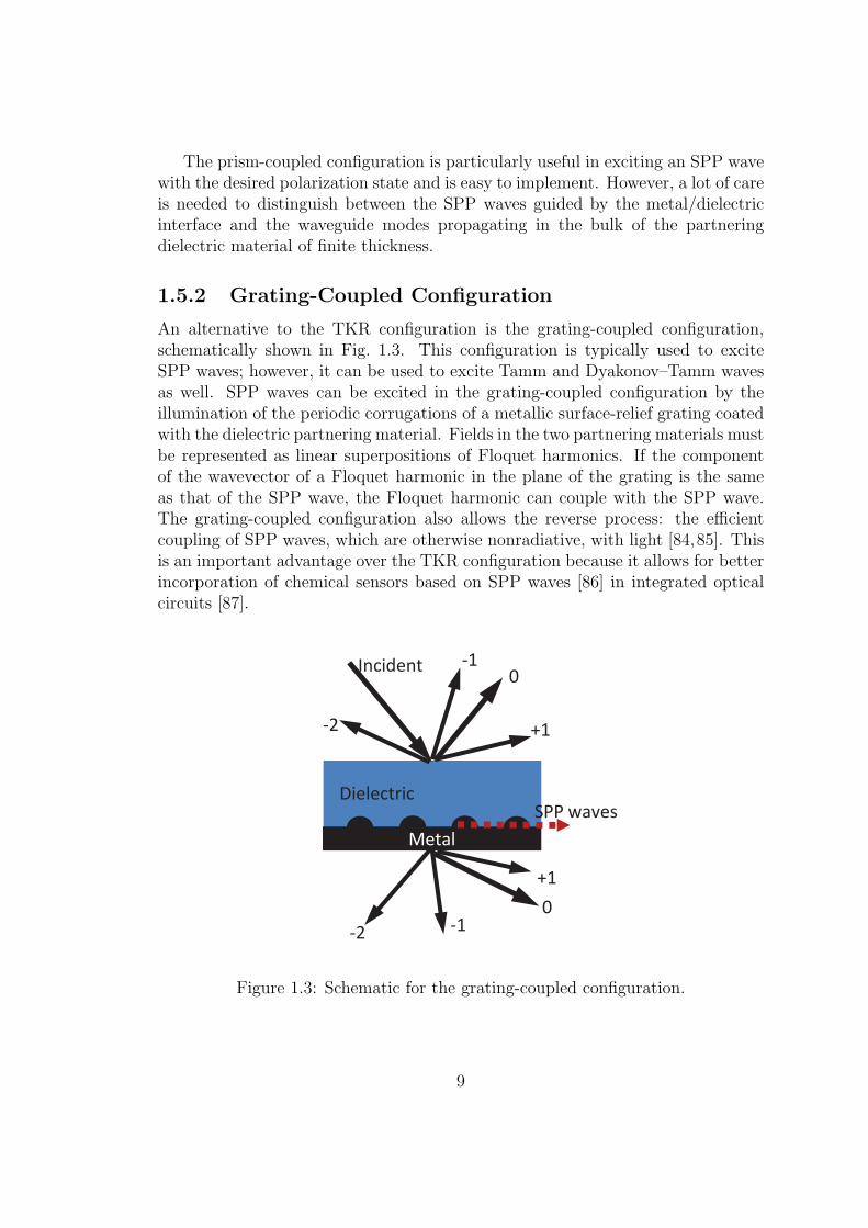
The prism-coupled configuration is particularly useful in exciting an SPP wavewith the desired polarization state and is easy to implement. However, a lot of careis needed to distinguish between the SPP waves guided by the metal/dielectricinterface and the waveguide modes propagating in the bulk of the partneringdielectric material of finite thickness.
1.5.2 Grating-Coupled Configuration
An alternative to the TKR configuration is the grating-coupled configuration,schematically shown in Fig. 1.3. This configuration is typically used to exciteSPP waves; however, it can be used to excite Tamm and Dyakonov–Tamm wavesas well. SPP waves can be excited in the grating-coupled configuration by theillumination of the periodic corrugations of a metallic surface-relief grating coatedwith the dielectric partnering material. Fields in the two partnering materials mustbe represented as linear superpositions of Floquet harmonics. If the componentof the wavevector of a Floquet harmonic in the plane of the grating is the sameas that of the SPP wave, the Floquet harmonic can couple with the SPP wave.The grating-coupled configuration also allows the reverse process: the efficientcoupling of SPP waves, which are otherwise nonradiative, with light [84,85]. Thisis an important advantage over the TKR configuration because it allows for betterincorporation of chemical sensors based on SPP waves [86] in integrated opticalcircuits [87].
SPP waves
Dielectric
Metal
Incident
Metal
0
+1
-1
-2
0
+1
-1 -2
Figure 1.3: Schematic for the grating-coupled configuration.
9
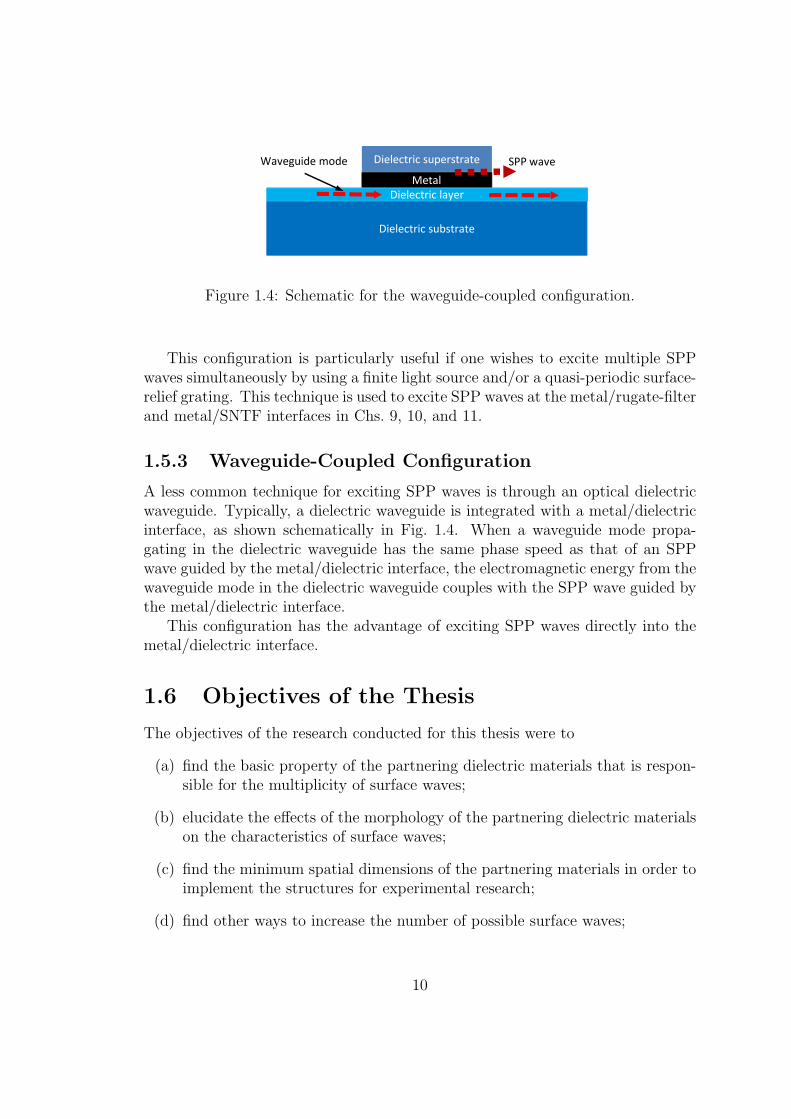
Dielectric superstrate
Metal
SPP wave
Dielectric layer
Dielectric substrate
Waveguide mode
Figure 1.4: Schematic for the waveguide-coupled configuration.
This configuration is particularly useful if one wishes to excite multiple SPPwaves simultaneously by using a finite light source and/or a quasi-periodic surface-relief grating. This technique is used to excite SPP waves at the metal/rugate-filterand metal/SNTF interfaces in Chs. 9, 10, and 11.
1.5.3 Waveguide-Coupled Configuration
A less common technique for exciting SPP waves is through an optical dielectricwaveguide. Typically, a dielectric waveguide is integrated with a metal/dielectricinterface, as shown schematically in Fig. 1.4. When a waveguide mode propa-gating in the dielectric waveguide has the same phase speed as that of an SPPwave guided by the metal/dielectric interface, the electromagnetic energy from thewaveguide mode in the dielectric waveguide couples with the SPP wave guided bythe metal/dielectric interface.
This configuration has the advantage of exciting SPP waves directly into themetal/dielectric interface.
1.6 Objectives of the Thesis
The objectives of the research conducted for this thesis were to
(a) find the basic property of the partnering dielectric materials that is respon-sible for the multiplicity of surface waves;
(b) elucidate the effects of the morphology of the partnering dielectric materialson the characteristics of surface waves;
(c) find the minimum spatial dimensions of the partnering materials in order toimplement the structures for experimental research;
(d) find other ways to increase the number of possible surface waves;
10
(e) study the excitation of multiple surface waves in prism- and grating-coupledconfigurations with periodically nonhomogeneous partnering dielectric ma-terials; and
(f) see if multiple SPP waves can lead to enhanced absorption of light in thin-film solar cells.
1.7 Organization of the Thesis
To achieve objectives (b) and (c) of the forgoing section, the canonical boundary-value problem of SPP-wave propagation guided by a single planar interface of ametal and an SNTF is formulated and solved in Ch. 2. A dispersion equation isobtained and solved to find the complex wavenumber for SPP waves which can beguided by the metal/SNTF interface. The spatial field and power profiles are alsogiven.
In Ch. 3, an interface of a metal and a rugate filter with a sinusoidal refrac-tive index profile is analyzed for objective (a) to elucidate the effect of periodicnonhomogeneity of the partnering dielectric material. The wavenumbers of thepossible SPP waves that can be supported by the metal/rugate-filter interface arefound as functions of the period of the rugate filter. In Ch. 4, the propagationof multiple Fano waves by an interface of a rugate filter and a material that hasa negative real permittivity is studied. This problem is an extension of the onesolved in Ch. 3.
To achieve objectives (b) and (c), Dyakonov–Tamm waves guided by a phase-twist combination defect in a periodically nonhomogeneous SNTF are studied inCh. 5. The phase defect is fixed at 180, whereas the twist defect is kept variableas also the direction of propagation, for numerical results. Multiple Dyakonov–Tamm waves that differ in spatial profile, degree of localization, and phase speedare found to propagate guided by the phase-twist combination defect, dependingon the angle between the morphologically significant planes of the SNTF on eitherside of the defect as well as on the direction of propagation.
SPP-wave propagation guided by a metallic slab inserted in a periodicallynonhomogeneous SNTF is considered in Ch. 6. The morphologically significantplanes of the SNTF on both sides of the metal slab could either be aligned ortwisted with respect to each other. The effect of slab thickness on the multiplicityand the spatial profiles of SPP waves is analyzed. In Ch. 7, the metal slab in theSNTF is replaced by a dielectric slab to study the effect of the coupling of thetwo interface on the propagation of Dyakonov–Tamm waves. The investigationspresented in Chs. 6 and 7 were conducted to achieve objective (d).
The excitation of multiple SPP waves at the metal/rugate-filter interface in theTKR and the grating-coupled configurations is studied, respectively, in Chs. 8 and9 to achieve objective (e). The results of the TKR and the grating-coupled con-
11
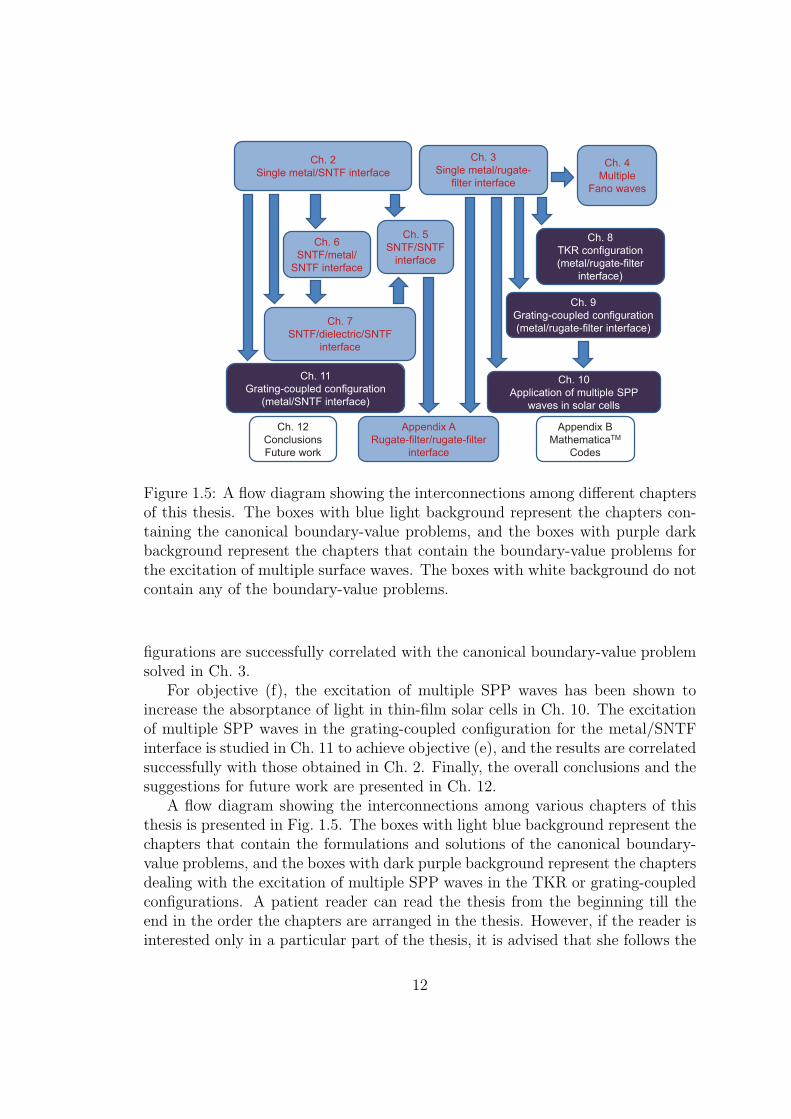
Ch. 2
Single metal/SNTF interface
Ch. 3
Single metal/rugate-
filter interface
Ch. 5
SNTF/SNTF
interface
Ch. 7
SNTF/dielectric/SNTF
interface
Ch. 4
Multiple
Fano waves
Ch. 6
SNTF/metal/
SNTF interface
Appendix A
Rugate-filter/rugate-filter
interface
Ch. 8
TKR configuration
(metal/rugate-filter
interface)
Ch. 9
Grating-coupled configuration
(metal/rugate-filter interface)
Ch. 10
Application of multiple SPP
waves in solar cells
Ch. 11
Grating-coupled configuration
(metal/SNTF interface)
Ch. 12
Conclusions
Future work
Appendix B
MathematicaTM
Codes
Figure 1.5: A flow diagram showing the interconnections among different chaptersof this thesis. The boxes with blue light background represent the chapters con-taining the canonical boundary-value problems, and the boxes with purple darkbackground represent the chapters that contain the boundary-value problems forthe excitation of multiple surface waves. The boxes with white background do notcontain any of the boundary-value problems.
figurations are successfully correlated with the canonical boundary-value problemsolved in Ch. 3.
For objective (f), the excitation of multiple SPP waves has been shown toincrease the absorptance of light in thin-film solar cells in Ch. 10. The excitationof multiple SPP waves in the grating-coupled configuration for the metal/SNTFinterface is studied in Ch. 11 to achieve objective (e), and the results are correlatedsuccessfully with those obtained in Ch. 2. Finally, the overall conclusions and thesuggestions for future work are presented in Ch. 12.
A flow diagram showing the interconnections among various chapters of thisthesis is presented in Fig. 1.5. The boxes with light blue background represent thechapters that contain the formulations and solutions of the canonical boundary-value problems, and the boxes with dark purple background represent the chaptersdealing with the excitation of multiple SPP waves in the TKR or grating-coupledconfigurations. A patient reader can read the thesis from the beginning till theend in the order the chapters are arranged in the thesis. However, if the reader isinterested only in a particular part of the thesis, it is advised that she follows the
12

flow diagram. For instance, if the reader wishes to read Ch. 11, she should beginwith Ch. 2 and then jump to to Ch. 11 or if the reader wishes to read Ch. 10,she should begin with Ch. 3 and then jump to Ch. 10—preferably going throughCh. 9 as well.
13

Chapter 2
SPP Waves Guided byMetal/SNTF Interface‡
2.1 Introduction
This chapter is devoted to the investigation on the propagation of a surface waveguided by the planar interface of a metal and an SNTF, the latter being peri-odically nonhomogeneous in the direction normal to the interface. In Refs. 70and 71, the absorptance, reflectance and transmittance of an incident linearly po-larized plane wave were calculated when this planar interface is implemented viaa metal-SNTF bilayer and a prism in the TKR configuration. The wavevector ofthe incident plane wave was supposed to lie wholly in the morphologically signifi-cant plane of the SNTF in Ref. 70, but that restriction was lifted in Ref. 71. Thecomputed results showed that multiple SPP waves, all of the same frequency orcolor, can be excited at the metal/SNTF interface. The guided SPP waves possessdifferent field structures as well as different phase speeds.
In Ref. 44, experimentally obtained data was presented in support of the theo-retical predictions of Ref. 70. The absorptances of two different metal-SNTF bilay-ers were evaluated as the difference between unity and the measured reflectance,the transmittance being assumed to be null-valued at angles of incidence exceed-ing the critical angle for the interface of the SNTF with the prism. Analysis ofthe collected data confirmed the possibility of exciting multiple SPP waves withdifferent phase speeds and field structures.
The method adopted for theoretical predictions and experimental verificationin Refs. 70, 71, and 44 was an indirect one, because the existence of SPP waveswas deduced from the absorptance, reflectance and transmittance characteristicsof a metal-SNTF bilayer. Each layer in the bilayer is of finite thickness. In the
‡This chapter is based on: M. Faryad, J. A. Polo Jr., and A. Lakhtakia, “Multiple trains ofsame-color surface plasmon-polaritons guided by the planar interface of a metal and a sculpturednematic thin film. Part IV: Canonical problem,” J. Nanophoton. 4, 043505 (2010).
14

canonical problem of SPP-wave propagation, the metal and the SNTF occupy half-spaces. The solution of the canonical problem provides incontrovertible proof ofthe existence of multiple SPP-wave modes, and also eliminates possible confusionwith waveguide modes spread over the entirety of the SNTF.
Accordingly, in this chapter, the goal was set to prove the existence of multipleSPP waves directly. The approach adopted is similar to that of Agarwal et al. [64],being independent of any incident plane wave. The formulated boundary-valueproblem was solved numerically for the SPP wavenumbers. The canonical problemis formulated in Sec. 2.2, and numerical results are presented and discussed inSec. 2.3. The concluding remarks are given in Sec. 2.4
2.2 Theory
Let the half-space z ≤ 0 be occupied by an isotropic and homogeneous metal withcomplex-valued relative permittivity scalar ϵm. The region z ≥ 0 is occupied bythe chosen SNTF as described in Sec. 1.3. Let the SPP wave propagate parallelto the unit vector ux cosψ + uy sinψ along the interface z = 0, and attenuate asz → ±∞. Therefore, in the region z ≤ 0, the wave vector may be written as
kmet = κ u1 − αmet uz , (2.1)
where κ2 + α2met = k20 ϵm, κ is complex-valued, and Im(αmet) > 0 for attenuation
as z → −∞; here and hereafter, the unit vectors u1 = ux cosψ + uy sinψ andu2 = −ux sinψ + uy cosψ. Accordingly, the field phasors in the metal may bewritten as
E(r) =
[ap
(αmet
k0
u1 +κ
k0
uz
)+ as u2
]exp(ikmet · r) , z ≤ 0 , (2.2)
and
H(r) = η−10
[−ap ϵmet u2 + as
(αmet
k0
u1 +κ
k0
uz
)]exp(ikmet · r) , z ≤ 0 . (2.3)
Here ap and as are unknown scalars with the same units as the electric field,with the subscripts p and s, respectively, denoting the parallel and perpendicularpolarization states with respect to the plane formed by u1 and uz.
For field representation in the SNTF, E(r) = e(z) exp (iκu1 · r) and H(r) =h(z) exp (iκu1 · r). The components ez(z) and hz(z) of the field phasors can befound in terms of the other components as follows:
ez(z) =ϵd(z) [ϵa(z)− ϵb(z)] sin [χ(z)] cos [χ(z)]
ϵa(z)ϵb(z)ex(z)
+κϵd(z)
ωϵ0ϵa(z)ϵb(z)[hx(z) sinψ − hy(z) cosψ] , z > 0 , (2.4)
hz(z) = − κ
ωµ0
[ex(z) sinψ − ey(z) cosψ] , z > 0 , (2.5)
15

where
ϵd(z) =ϵa(z) ϵb(z)
ϵa(z) cos2 [χ(z)] + ϵb(z) sin2 [χ(z)]
. (2.6)
The other components of the electric and magnetic field phasors are used inthe column vector
[f(z)] = [ex(z) ey(z) hx(z) hy(z)]T (2.7)
which satisfies the matrix differential equation [64]
d
dz[f(z)] = i
[P (z)
]· [f(z)] , z > 0 , (2.8)
where the 4×4 matrix
[P (z)] = ω
0 0 0 µ0
0 0 −µ0 00 −ϵ0 ϵc(z) 0 0
ϵ0 ϵd(z) 0 0 0
+κϵd(z) [ϵa(z)− ϵb(z)]
ϵa(z) ϵb(z)sin [χ(z)] cos [χ(z)]
cosψ 0 0 0sinψ 0 0 00 0 0 00 0 − sinψ cosψ
+κ2
ωϵ0
ϵd(z)
ϵa(z) ϵb(z)
0 0 cosψ sinψ − cos2 ψ0 0 sin2 ψ − cosψ sinψ0 0 0 00 0 0 0
+κ2
ωµ0
0 0 0 00 0 0 0
− cosψ sinψ cos2 ψ 0 0− sin2 ψ cosψ sinψ 0 0
. (2.9)
The piecewise uniform approximation technique [1] is used to determine thematrix [Q] that appears in the relation
[f(2Ω)] = [Q] · [f(0+)] (2.10)
to characterize the optical response of one period of the chosen SNTF for specificvalues of κ and ψ. By virtue of the Floquet–Lyapunov theorem [88], a matrix [Q]
can be defined such that[Q] = exp
i2Ω[Q]
. (2.11)
16

Both [Q] and [Q] share the same eigenvectors, and their eigenvalues are also re-
lated. Let [t](n), n ∈ [1, 4], be the eigenvector corresponding to the nth eigenvalueσn of [Q]; then, the corresponding eigenvalue αn of [Q] is given by
αn = −i lnσn2Ω
, n ∈ [1, 4] . (2.12)
After ensuring that Im(α1,2) > 0,
[f(0+)] =[[t](1) [t](2)
]·[b1b2
](2.13)
for SPP-wave propagation, where b1 and b2 are unknown dimensionless scalars;the other two eigenvalues of [Q] pertain to waves that amplify as z → ∞ and
cannot therefore contribute to the SPP wave. At the same time,
[f(0−)] =
αmet
k0cosψ − sinψ
αmet
k0sinψ cosψ
ϵmet
η0sinψ αmet
k0η0cosψ
− ϵmet
η0cosψ αmet
k0η0sinψ
·[apas
], (2.14)
by virtue of (2.2) and (2.3). Continuity of the tangential components of the electricand magnetic field phasors across the plane z = 0 requires that [f(0−)] = [f(0+)],which may be rearranged as the matrix equation
[Y ] ·
apasb1b2
=
0000
. (2.15)
For a nontrivial solution, the 4×4 matrix [Y ] must be singular, so that
det [Y ] = 0 (2.16)
is the dispersion equation for the SPP wave. This equation has to be solved inorder to determine the SPP wavenumber κ.
2.3 Numerical Results and Discussion
A MathematicaTM program was written and implemented to solve (2.16) using theNewton–Raphson method [89] to obtain κ for a specific value of ψ. The program isprovided in Appendix B.1. The solutions of the dispersion equation were searchedwhen Re [κ/k0] > 1. The free-space wavelength was fixed at λ0 = 633 nm. The
17

0 20 40 60 80
1.9
2.0
2.1
2.2
2.3
2.4
2.5
Ψ HdegLR
e@Κ
k 0D
0 20 40 60 80
0.01
0.02
0.03
0.04
0.05
Ψ HdegL
Im@Κ
k 0D
Figure 2.1: (left) Real and (right) imaginary parts of κ as functions of ψ, for SPP-wave propagation guided by the planar interface of aluminum and a titanium-oxideSNTF. Either two or three modes are possible, depending on ψ.
-0.4 -0.3 -0.2 -0.1 0.00
2
4
6
8
z W
Èe81
,2,z<È
0.0 0.5 1.0 1.5 2.00
10
20
30
z W
Èe81
,2,z<È
-0.4 -0.3 -0.2 -0.1 0.00.00
0.05
0.10
0.15
0.20
z W
Èh81
,2,z<È
0.0 0.5 1.0 1.5 2.00.00
0.05
0.10
0.15
0.20
z W
Èh81
,2,z<È
-0.4 -0.3 -0.2 -0.1 0.0-0.20
-0.15
-0.10
-0.05
0.00
z W
P81
,2,z<
0.0 0.5 1.0 1.5 2.00.0
0.5
1.0
1.5
2.0
2.5
z W
P81
,2,z<
Figure 2.2: Variations of components of e (in V m−1), h (in A m−1), and P (inW m−2) with z along the line x = 0, y = 0, for κ = (2.455 + i0.04208)k0 andψ = 0. The components parallel to u1, u2, and uz, are represented by black solid,red dashed, and blue chain-dashed lines, respectively. The data were computedby setting ap = 1 V m−1, with as = 0, b1 = 0, and b2 = −1.3026 − i7.9841 thenobtained using (2.15).
metal was taken to be aluminum: ϵm = −56 + i21. As in Ref. 71, the angles χv
and δv were taken to be 45 and 30, respectively, and Ω = 200 nm for all results
18
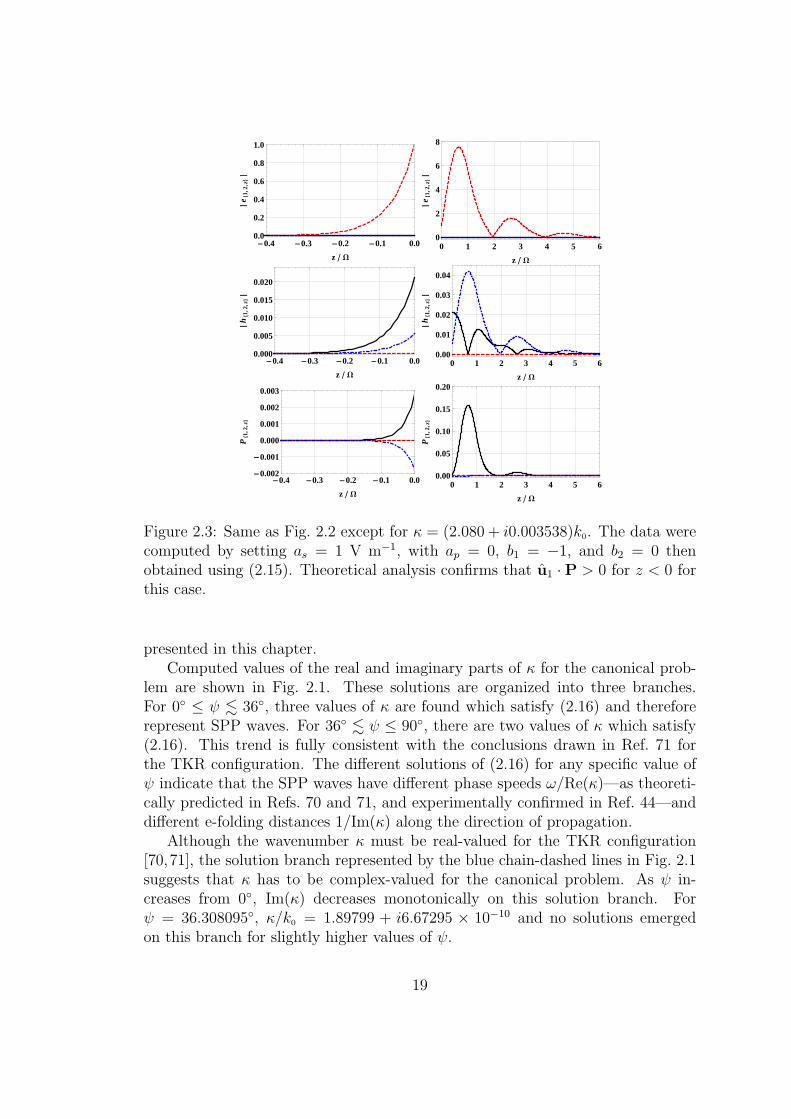
-0.4 -0.3 -0.2 -0.1 0.00.0
0.2
0.4
0.6
0.8
1.0
z W
Èe81
,2,z<È
0 1 2 3 4 5 60
2
4
6
8
z W
Èe81
,2,z<È
-0.4 -0.3 -0.2 -0.1 0.00.000
0.005
0.010
0.015
0.020
z W
Èh81
,2,z<È
0 1 2 3 4 5 60.00
0.01
0.02
0.03
0.04
z W
Èh81
,2,z<È
-0.4 -0.3 -0.2 -0.1 0.0-0.002
-0.001
0.000
0.001
0.002
0.003
z W
P81
,2,z<
0 1 2 3 4 5 60.00
0.05
0.10
0.15
0.20
z W
P81
,2,z<
Figure 2.3: Same as Fig. 2.2 except for κ = (2.080 + i0.003538)k0. The data werecomputed by setting as = 1 V m−1, with ap = 0, b1 = −1, and b2 = 0 thenobtained using (2.15). Theoretical analysis confirms that u1 ·P > 0 for z < 0 forthis case.
presented in this chapter.Computed values of the real and imaginary parts of κ for the canonical prob-
lem are shown in Fig. 2.1. These solutions are organized into three branches.For 0 ≤ ψ . 36, three values of κ are found which satisfy (2.16) and thereforerepresent SPP waves. For 36 . ψ ≤ 90, there are two values of κ which satisfy(2.16). This trend is fully consistent with the conclusions drawn in Ref. 71 forthe TKR configuration. The different solutions of (2.16) for any specific value ofψ indicate that the SPP waves have different phase speeds ω/Re(κ)—as theoreti-cally predicted in Refs. 70 and 71, and experimentally confirmed in Ref. 44—anddifferent e-folding distances 1/Im(κ) along the direction of propagation.
Although the wavenumber κ must be real-valued for the TKR configuration[70,71], the solution branch represented by the blue chain-dashed lines in Fig. 2.1suggests that κ has to be complex-valued for the canonical problem. As ψ in-creases from 0, Im(κ) decreases monotonically on this solution branch. Forψ = 36.308095, κ/k0 = 1.89799 + i6.67295 × 10−10 and no solutions emergedon this branch for slightly higher values of ψ.
19
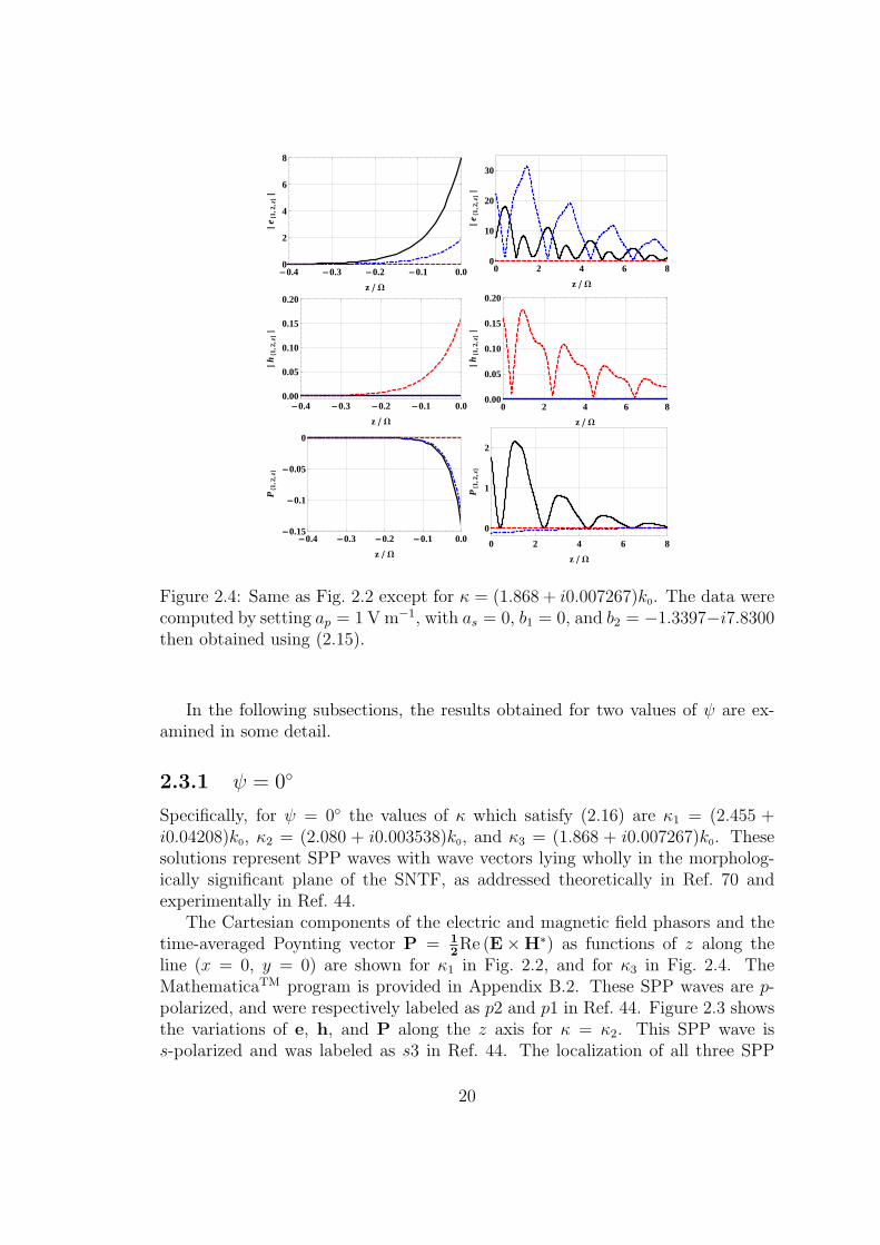
-0.4 -0.3 -0.2 -0.1 0.00
2
4
6
8
z W
Èe81
,2,z<È
0 2 4 6 80
10
20
30
z W
Èe81
,2,z<È
-0.4 -0.3 -0.2 -0.1 0.00.00
0.05
0.10
0.15
0.20
z W
Èh81
,2,z<È
0 2 4 6 80.00
0.05
0.10
0.15
0.20
z W
Èh81
,2,z<È
-0.4 -0.3 -0.2 -0.1 0.0
0
-0.05
-0.1
-0.15
z W
P81
,2,z<
0 2 4 6 8
0
1
2
z W
P81
,2,z<
Figure 2.4: Same as Fig. 2.2 except for κ = (1.868 + i0.007267)k0. The data werecomputed by setting ap = 1 V m−1, with as = 0, b1 = 0, and b2 = −1.3397−i7.8300then obtained using (2.15).
In the following subsections, the results obtained for two values of ψ are ex-amined in some detail.
2.3.1 ψ = 0
Specifically, for ψ = 0 the values of κ which satisfy (2.16) are κ1 = (2.455 +i0.04208)k0, κ2 = (2.080 + i0.003538)k0, and κ3 = (1.868 + i0.007267)k0. Thesesolutions represent SPP waves with wave vectors lying wholly in the morpholog-ically significant plane of the SNTF, as addressed theoretically in Ref. 70 andexperimentally in Ref. 44.
The Cartesian components of the electric and magnetic field phasors and thetime-averaged Poynting vector P = 1
2Re (E×H∗) as functions of z along the
line (x = 0, y = 0) are shown for κ1 in Fig. 2.2, and for κ3 in Fig. 2.4. TheMathematicaTM program is provided in Appendix B.2. These SPP waves are p-polarized, and were respectively labeled as p2 and p1 in Ref. 44. Figure 2.3 showsthe variations of e, h, and P along the z axis for κ = κ2. This SPP wave iss-polarized and was labeled as s3 in Ref. 44. The localization of all three SPP
20
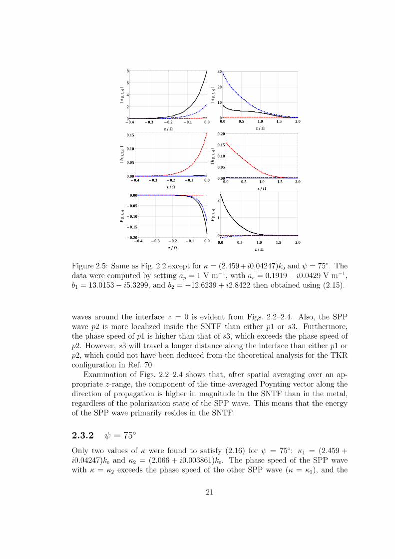
-0.4 -0.3 -0.2 -0.1 0.00
2
4
6
8
z W
Èe81
,2,z<È
0.0 0.5 1.0 1.5 2.00
10
20
30
z W
Èe81
,2,z<È
-0.4 -0.3 -0.2 -0.1 0.00.00
0.05
0.10
0.15
z W
Èh81
,2,z<È
0.0 0.5 1.0 1.5 2.00.00
0.05
0.10
0.15
0.20
z W
Èh81
,2,z<È
-0.4 -0.3 -0.2 -0.1 0.0-0.20
-0.15
-0.10
-0.05
0.00
z W
P81
,2,z<
0.0 0.5 1.0 1.5 2.0
0
1
2
z W
P81
,2,z<
Figure 2.5: Same as Fig. 2.2 except for κ = (2.459+ i0.04247)k0 and ψ = 75. Thedata were computed by setting ap = 1 V m−1, with as = 0.1919− i0.0429 V m−1,b1 = 13.0153− i5.3299, and b2 = −12.6239 + i2.8422 then obtained using (2.15).
waves around the interface z = 0 is evident from Figs. 2.2–2.4. Also, the SPPwave p2 is more localized inside the SNTF than either p1 or s3. Furthermore,the phase speed of p1 is higher than that of s3, which exceeds the phase speed ofp2. However, s3 will travel a longer distance along the interface than either p1 orp2, which could not have been deduced from the theoretical analysis for the TKRconfiguration in Ref. 70.
Examination of Figs. 2.2–2.4 shows that, after spatial averaging over an ap-propriate z-range, the component of the time-averaged Poynting vector along thedirection of propagation is higher in magnitude in the SNTF than in the metal,regardless of the polarization state of the SPP wave. This means that the energyof the SPP wave primarily resides in the SNTF.
2.3.2 ψ = 75
Only two values of κ were found to satisfy (2.16) for ψ = 75: κ1 = (2.459 +i0.04247)k0 and κ2 = (2.066 + i0.003861)k0. The phase speed of the SPP wavewith κ = κ2 exceeds the phase speed of the other SPP wave (κ = κ1), and the
21

-0.4 -0.3 -0.2 -0.1 0.00
5
10
15
z WÈ
e81
,2,z<È
0 1 2 3 4 5 60
40
80
120
z W
Èe81
,2,z<È
-0.4 -0.3 -0.2 -0.1 0.00.0
0.1
0.2
0.3
0.4
z W
Èh81
,2,z<È
0 1 2 3 4 5 60.0
0.2
0.4
0.6
0.8
z W
Èh81
,2,z<È
-0.4 -0.3 -0.2 -0.1 0.0
-0.4
-0.2
0.0
0.2
0.4
z W
P81
,2,z<
0 1 2 3 4 5 60
10
20
30
40
z W
P81
,2,z<
Figure 2.6: Same as Fig. 2.2 except for κ = (2.066+i0.003861)k0 and ψ = 75. Thedata were computed by setting ap = 1 V m−1, with as = −15.9578+i3.4826 V m−1,b1 = −17.8249− i35.4678, and b2 = 25.4223+ i31.0644 then obtained using (2.15).
former SPP wave will propagate a longer distance along the interface than thelatter SPP wave.
The variations of e, h, and P along the z axis are shown in Fig. 2.5 for κ1, andin Fig. 2.6 for κ2. These two SPP waves cannot be rigorously classified as eitherp- or s-polarized, which is consistent with the deductions in Ref. 71 for the TKRconfiguration. However, the electric field in Fig. 2.5 is predominantly oriented inthe plane formed by u1 and uz, thereby suggesting that the SPP wave for κ1 couldbe classified as quasi-p-polarized on both sides of the interface. In contrast, theelectric field in Fig. 2.6 is predominantly oriented parallel to u2, which impliesthat the SPP wave for κ2 is quasi-s-polarized on both sides of the interface.
Finally, it can be deduced from Figs. 2.5 and 2.6 that the energy content ofeither SPP wave for ψ = 75 resides primarily in the SNTF, just as of any of thethree SPP waves for ψ = 0.
22
2.4 Concluding Remarks
The solution of the canonical boundary-value problem
(i) proved directly that multiple SPP waves of the same frequency but differentphase speeds, attenuation rates, spatial profiles, and polarization states canbe guided by the planar interface of semi-infinite expanses of the metal andthe periodically nonhomogeneous SNTF; and
(ii) not only upheld the conclusions obtained in Refs. 44, 70 and 71, but alsogave additional information on the e-folding distance along the direction ofpropagation and the spatial extent of the SPP waves into the metal and theSNTF.
The excitation of multiple SPP waves at the metal/SNTF interface is studiedin Ch. 11 and the results of that chapter are successfully correlated with thoseobtained in this chapter.
23

Chapter 3
SPP Waves Guided byMetal/Rugate-Filter Interface‡
3.1 Introduction
At a specific frequency, the solution of a canonical boundary-value problem [13,14, 35] shows that only one SPP wave can propagate along the interface, if thepartnering dielectric material is isotropic and homogeneous. The same conclusionholds true even if that material is anisotropic [20]– [42]. However, if the partneringdielectric material is both anisotropic and periodically nonhomogeneous in thedirection normal to the interface, the solutions of the canonical boundary-valueproblem [26], as is also shown in Ch. 2, shows that more than one SPP waves—withdifferent phase speeds, attenuation rates, and field distributions, but of the samefrequency [27]—can propagate guided by the interface. Experimental verificationof this theoretical prediction has been found [43,44].
On the basis of foregoing discussion, it can be hypothesized that the phe-nomenon of the propagation of multiple SPP waves guided by a single interfacecould simply be due to the periodic nonhomogeneity of the dielectric partneringmaterial. In order to test this hypothesis, a canonical problem involving two half-spaces is set up, one filled homogeneously with a metal, the other occupied by anisotropic dielectric material whose refractive index varies sinusoidally along thenormal direction (as in a rugate filter [2,74]). The canonical boundary-value prob-lem is formulated in Sec. 3.2, and numerical results are presented and discussedin Sec. 3.3. Concluding remarks are presented in Sec. 3.4.
‡This chapter is based on: M. Faryad and A. Lakhtakia, “On surface plasmon-polariton wavesguided by the interface of a metal and a rugate filter with sinusoidal refractive-index profile,” J.Opt. Soc. Am. B 27, 2218–2223 (2010).
24

3.2 Theory
Let the half-space z ≤ 0 be occupied by an isotropic and homogeneous metal withcomplex-valued relative permittivity scalar ϵm. The region z ≥ 0 is occupied by arugate filter with relative permittivity
ϵd(z) =
[(nb + na
2
)+
(nb − na
2
)sin(πz
Ω
)]2, (3.1)
where na and nb are lowest and highest indexes of refraction, respectively, and 2Ωis the period.
Without loss of generality, let the SPP wave propagate parallel to the unitvector ux guided by the interface z = 0, and attenuate as z → ±∞. Therefore, inthe region z ≤ 0, the wave vector may be written as
kmet = κ ux − αmet uz , (3.2)
where κ2+α2met = k20 ϵm, κ is complex-valued, and Im(αmet) > 0 for attenuation as
z → −∞. Accordingly, the field phasors in the metallic half-space may be writtenas
E(r) =
[ap
(αmet
k0
ux +κ
k0
uz
)+ as uy
]exp(ikmet · r) , z ≤ 0 , (3.3)
and
H(r) = η−10
[−ap ϵmet uy + as
(αmet
k0
ux +κ
k0
uz
)]exp(ikmet · r) , z ≤ 0 . (3.4)
Here ap and as are unknown scalars with the same units as the electric field, and thesubscripts p and s, respectively, denote the p- (parallel-) and s- (perpendicular-)polarization states with respect to the xz plane.
For field representation in the rugate filter, let me write E(r) = e(z) exp (iκx)and H(r) = h(z) exp (iκx). The components ez(z) and hz(z) of the field phasorscan be found in terms of the other components as follows:
ez(z) = − κ
ωϵ0ϵr(z)hy(z), z > 0 , (3.5)
hz(z) =κ
ωµ0
ey(z), z > 0 . (3.6)
The other components of the electric and magnetic field phasors are used in thecolumn vector
[f(z)] = [ex(z) ey(z) hx(z) hy(z)]T (3.7)
which satisfies the matrix ordinary differential equation
d
dz[f(z)] = i
[P (z)
]· [f(z)] , z > 0 , (3.8)
25
where the 4×4 matrix
[P (z)] = ω
0 0 0 µ0
0 0 −µ0 00 −ϵ0 ϵd(z) 0 0
ϵ0 ϵd(z) 0 0 0
+κ2
ωϵ0ϵd(z)µ0
0 0 0 −µ0
0 0 0 00 ϵ0ϵd(z) 0 00 0 0 0
. (3.9)
The 4×4 matrix ordinary differential equation (3.8) can be partitioned intotwo autonomous 2×2 matrix ordinary differential equations, one for p-polarizedlight involving ex, hy and the other for s-polarized light involving ey, hx, butit would be better to treat Eq. (3.8) as a whole for both linear polarization statessimultaneously, to have a holistic view of the problem. The piecewise uniform ap-proximation technique [1] to determine the matrix [Q] that appears in the relation
[f(2Ω)] = [Q] · [f(0+)] (3.10)
to characterize the optical response of one period of the rugate filter for specificvalues of κ.
By virtue of the Floquet–Lyapunov theorem [88], a matrix [Q] can be defined
such that[Q] = exp
i2Ω[Q]
. (3.11)
Both [Q] and [Q] share the same (linearly independent) eigenvectors, and their
eigenvalues are also related. Let [t](n), n ∈ [1, 4], be the eigenvector correspondingto the nth eigenvalue σn of [Q]; then, the corresponding eigenvalue αn of [Q] is
given by
αn = −i lnσn2Ω
, n ∈ [1, 4] . (3.12)
After labeling the eigenvalues of [Q] such that Im(α1,2) > 0,it is set [94]
[f(0+)] =[[t](1) [t](2)
]·[b1b2
](3.13)
for SPP-wave propagation, where b1 and b2 are unknown dimensionless scalars;the other two eigenvalues of [Q] pertain to waves that amplify as z → ∞ and
cannot therefore contribute to the SPP wave. At the same time,
[f(0−)] =
αmet
k00
0 1
0 αmet
k0η0
− ϵmet
η00
·[apas
], (3.14)
26

by virtue of Eqs. (3.3) and (3.4). Continuity of the tangential components of theelectric and magnetic field phasors across the plane z = 0 requires that [f(0−)] =[f(0+)], which may be rearranged as the matrix equation
[Y ] ·
apasb1b2
=
0000
. (3.15)
For a nontrivial solution, the 4×4 matrix [Y ] must be singular, so that
det [Y ] = 0 (3.16)
is the dispersion equation for the SPP wave. This equation has to be solved inorder to determine the SPP wavenumber κ.
3.3 Numerical Results and Discussion
A MathematicaTM program was written and implemented to solve Eq. (3.16)using the Newton–Raphson method [89], and the solutions were searched whenRe [κ/k0] > 1. The free-space wavelength was fixed at λ0 = 633 nm, and the metalwas taken to be bulk aluminum: ϵm = −56 + i21. While Ω was kept variable, theminimum and maximum indexes of refraction of the rugate filter were fixed froman example provided by Baumeister [74]: na = 1.45 and nb = 2.32.
The solutions of the dispersion equation, calculated for 0.005 ≤ Ω/λ0 ≤ 2, areshown in Fig. 3.11. These solutions are organized in 16 branches: eight brancheslabeled as s1–s8 represent SPP waves with the s-polarization state, and eightbranches labeled as p1–p8 represent SPP waves with the p-polarization state. Atany value of Ω ≥ 0.145λ0, there are more than one possible SPP waves. Evidencefor the excitement of s-polarized SPP waves guided by the interface of a metaland an isotropic dielectric material does exist, although it is very rare [33,47].
Clearly from Fig. 3.1, more than one SPP waves can propagate for Ω ≥ 0.145λ0.These SPP waves have different phase speeds ω/Re(κ) and attenuation rates1/Im(κ). As both partnering materials are isotropic, this multiplicity must besurely due to the periodic nonhomogeneity of the dielectric partnering mate-rial (i.e., the rugate filter)—which is the chief result presented in this chapter.Although the observability of two SPP waves—one of either linear polarizationstate—when the partnering dielectric material is periodically nonhomogeneousin a piecewise uniform fashion had recently been established numerically for the
1Figures 3.1 and 3.4 are updated versions of Figs. 1 and 4, respectively, in: M. Faryad andA. Lakhtakia, “On surface plasmon-polariton waves guided by the interface of a metal and arugate filter with sinusoidal refractive-index profile,” J. Opt. Soc. Am. B 27, 2218–2223 (2010).
27
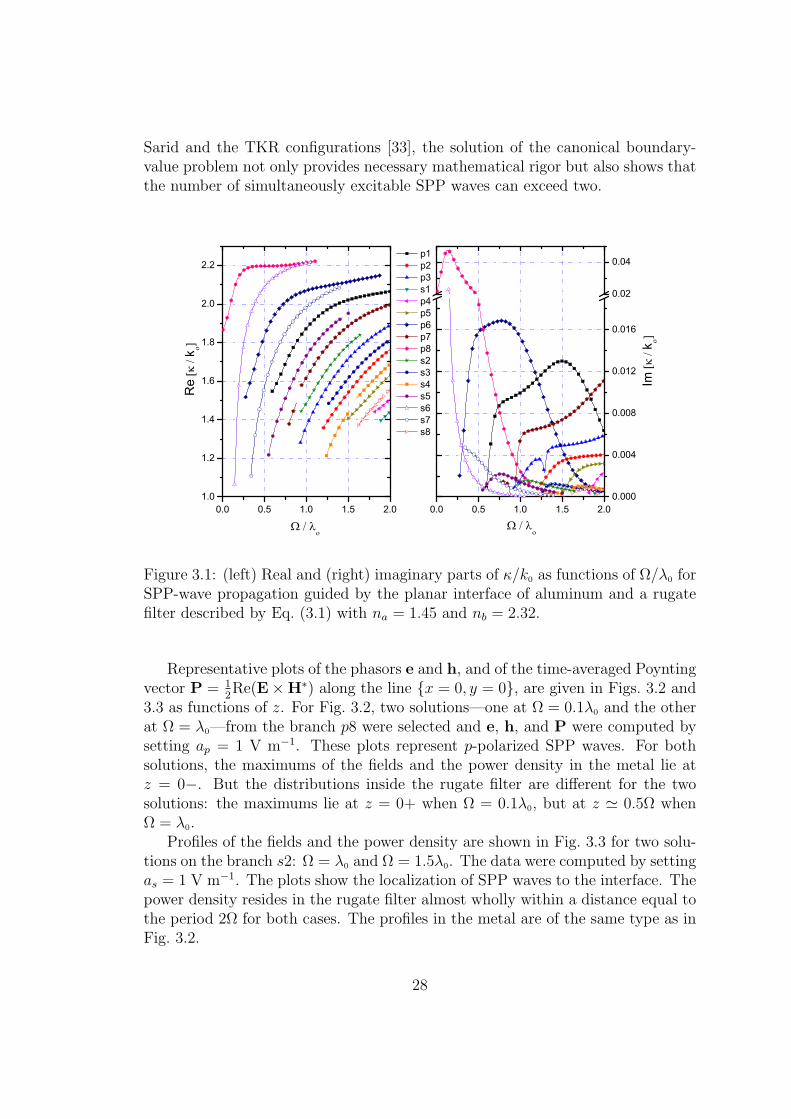
Sarid and the TKR configurations [33], the solution of the canonical boundary-value problem not only provides necessary mathematical rigor but also shows thatthe number of simultaneously excitable SPP waves can exceed two.
0.0 0.5 1.0 1.5 2.01.0
1.2
1.4
1.6
1.8
2.0
2.2
0.0 0.5 1.0 1.5 2.00.000
0.004
0.008
0.012
0.016
0.02
0.04
Imk
Re
k
p1 p2 p3 s1 p4 p5 p6 p7 p8 s2 s3 s4 s5 s6 s7 s8
Figure 3.1: (left) Real and (right) imaginary parts of κ/k0 as functions of Ω/λ0 forSPP-wave propagation guided by the planar interface of aluminum and a rugatefilter described by Eq. (3.1) with na = 1.45 and nb = 2.32.
Representative plots of the phasors e and h, and of the time-averaged Poyntingvector P = 1
2Re(E×H∗) along the line x = 0, y = 0, are given in Figs. 3.2 and
3.3 as functions of z. For Fig. 3.2, two solutions—one at Ω = 0.1λ0 and the otherat Ω = λ0—from the branch p8 were selected and e, h, and P were computed bysetting ap = 1 V m−1. These plots represent p-polarized SPP waves. For bothsolutions, the maximums of the fields and the power density in the metal lie atz = 0−. But the distributions inside the rugate filter are different for the twosolutions: the maximums lie at z = 0+ when Ω = 0.1λ0, but at z ≃ 0.5Ω whenΩ = λ0.
Profiles of the fields and the power density are shown in Fig. 3.3 for two solu-tions on the branch s2: Ω = λ0 and Ω = 1.5λ0. The data were computed by settingas = 1 V m−1. The plots show the localization of SPP waves to the interface. Thepower density resides in the rugate filter almost wholly within a distance equal tothe period 2Ω for both cases. The profiles in the metal are of the same type as inFig. 3.2.
28
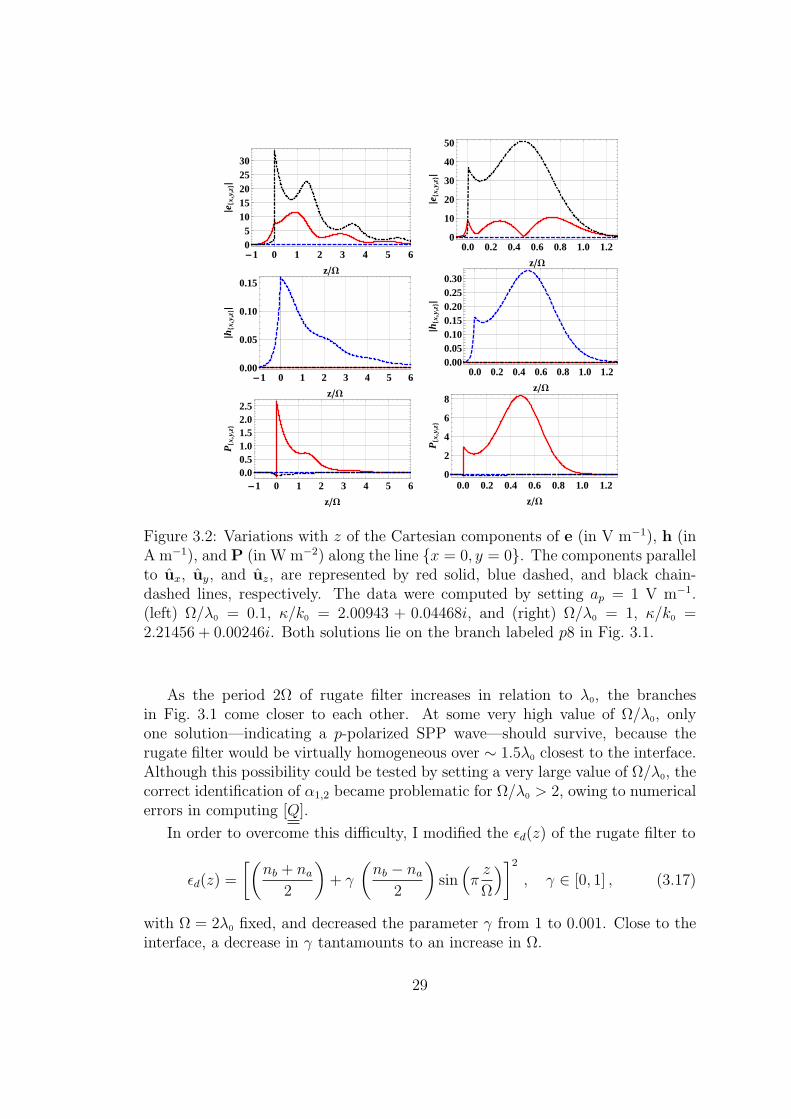
-1 0 1 2 3 4 5 605
1015202530
zW
Èe8x
,y,z<È
-1 0 1 2 3 4 5 60.00
0.05
0.10
0.15
zW
Èh8x
,y,z<È
-1 0 1 2 3 4 5 60.00.51.01.52.02.5
zW
P8x
,y,z<
0.0 0.2 0.4 0.6 0.8 1.0 1.20
10
20
30
40
50
zW
Èe8x
,y,z<È
0.0 0.2 0.4 0.6 0.8 1.0 1.20.000.050.100.150.200.250.30
zW
Èh8x
,y,z<È
0.0 0.2 0.4 0.6 0.8 1.0 1.20
2
4
6
8
zW
P8x
,y,z<
Figure 3.2: Variations with z of the Cartesian components of e (in V m−1), h (inA m−1), and P (in W m−2) along the line x = 0, y = 0. The components parallelto ux, uy, and uz, are represented by red solid, blue dashed, and black chain-dashed lines, respectively. The data were computed by setting ap = 1 V m−1.(left) Ω/λ0 = 0.1, κ/k0 = 2.00943 + 0.04468i, and (right) Ω/λ0 = 1, κ/k0 =2.21456 + 0.00246i. Both solutions lie on the branch labeled p8 in Fig. 3.1.
As the period 2Ω of rugate filter increases in relation to λ0, the branchesin Fig. 3.1 come closer to each other. At some very high value of Ω/λ0, onlyone solution—indicating a p-polarized SPP wave—should survive, because therugate filter would be virtually homogeneous over ∼ 1.5λ0 closest to the interface.Although this possibility could be tested by setting a very large value of Ω/λ0, thecorrect identification of α1,2 became problematic for Ω/λ0 > 2, owing to numericalerrors in computing [Q].
In order to overcome this difficulty, I modified the ϵd(z) of the rugate filter to
ϵd(z) =
[(nb + na
2
)+ γ
(nb − na
2
)sin(πz
Ω
)]2, γ ∈ [0, 1] , (3.17)
with Ω = 2λ0 fixed, and decreased the parameter γ from 1 to 0.001. Close to theinterface, a decrease in γ tantamounts to an increase in Ω.
29

-1 0 1 2 3 4 50
2
4
6
8
zW
Èe8x
,y,z<È
-1 0 1 2 3 4 50.0000.0050.0100.0150.0200.0250.030
zW
Èh8x
,y,z<È
-1 0 1 2 3 4 50.000.020.040.060.080.100.12
zW
P8x
,y,z<
-0.5 0.0 0.5 1.0 1.5 2.00
2
4
6
8
10
zW
Èe8x
,y,z<È
-0.5 0.0 0.5 1.0 1.5 2.00.00
0.01
0.02
0.03
0.04
zW
Èh8x
,y,z<È
-0.5 0.0 0.5 1.0 1.5 2.00.000.050.100.150.20
zW
P8x
,y,z<
Figure 3.3: Same as Fig. 3.2 except for (left) Ω/λ0 = 1, κ/k0 = 1.4864+0.0013203i,and (right) Ω/λ0 = 1.5, κ/k0 = 1.7873 + 0.0007801i, and the data were computedby setting as = 1 V m−1. Both solutions lie on the branch labeled s2 in Fig. 3.1.
In Fig. 3.4, the calculated solutions of the dispersion equation are organized asfunctions of γ ∈ [0.001, 1] in nine branches. The branches labeled as p1–p5, p7, s1,s4, and s8 are continuations of the similarly labeled branches in Fig. 3.1, while twonew branches—p9 and p10—emerge. All solution branches in Figs. 3.1 and 3.4 dieout when the imaginary part of κ decreases to zero, the sole exception being thebranch p10. This branch extends to γ = 0.001 in Fig. 3.4. As γ decreases evenfurther, the branch p10 approaches the solution for a metal/dielectric interfacewith the relative permittivity of the dielectric partnering material uniform at ϵd =(1/4) (na + nb)
2. For instance, at γ = 0.001, the solution of the dispersion equationgives a p-polarized SPP wave with wavenumber κ = (1.9395 + 0.02140i)k0, whilethe p-polarized wave at the interface of aluminum and a homogeneous isotropicdielectric with relative permittivity ϵd = 3.5532 has wavenumber κ = (1.9394 +0.02141i)k0 [34, 35].
Figure 3.5 shows the profiles of the fields and the time-averaged Poynting vectorfor (i) γ = 0.5 and κ/k0 = 1.78142+ 0.00288i on the branch labeled p3 in Fig. 3.4and (ii) γ = 0.1 and κ/k0 = 1.9515 + 0.01943i on the branch labeled p10 in thesame figure. Strong localization to the interface of the metal and the rugate filter
30
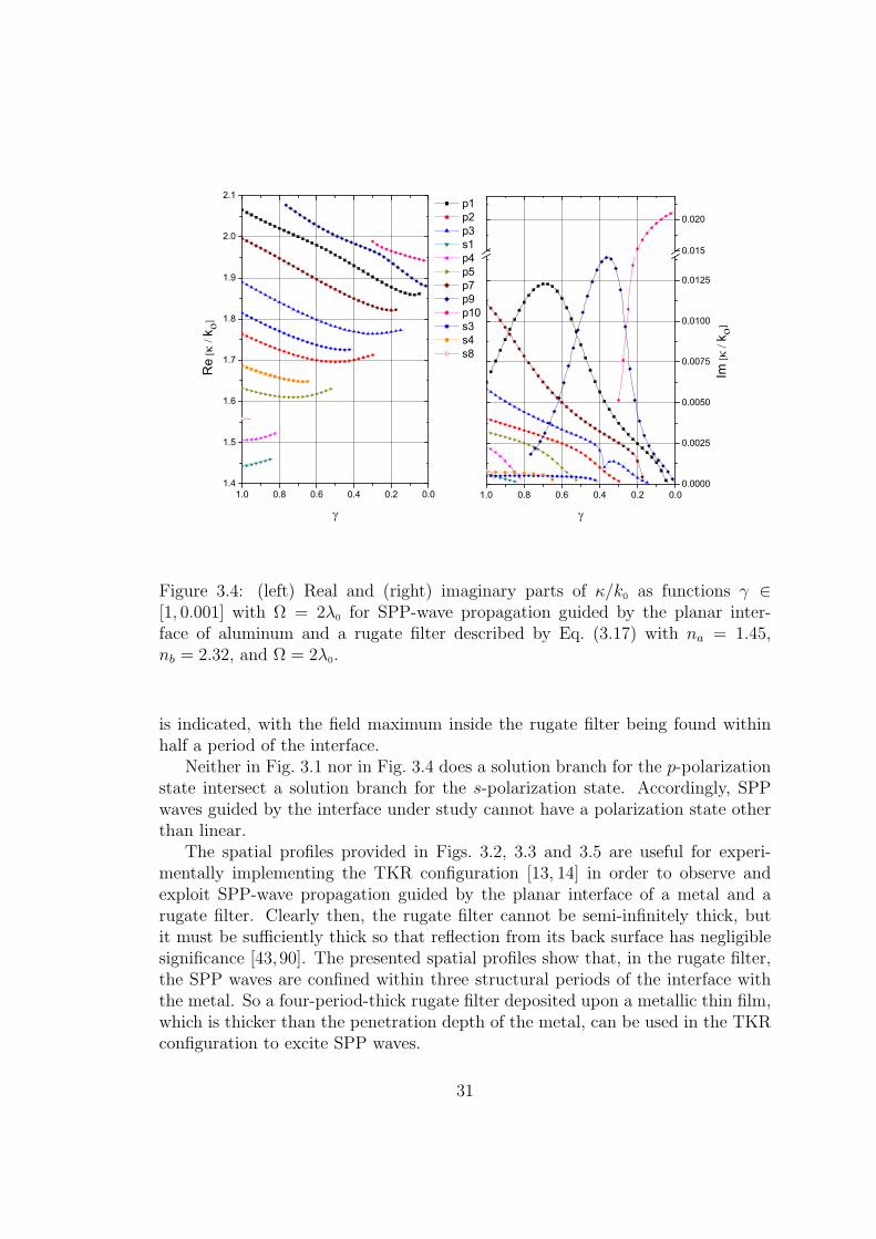
1.0 0.8 0.6 0.4 0.2 0.01.4
1.5
1.6
1.7
1.8
1.9
2.0
2.1
1.0 0.8 0.6 0.4 0.2 0.00.0000
0.0025
0.0050
0.0075
0.0100
0.0125
0.015
0.020 p1 p2 p3 s1 p4 p5 p7 p9 p10 s3 s4 s8
Re
k
Imk
Figure 3.4: (left) Real and (right) imaginary parts of κ/k0 as functions γ ∈[1, 0.001] with Ω = 2λ0 for SPP-wave propagation guided by the planar inter-face of aluminum and a rugate filter described by Eq. (3.17) with na = 1.45,nb = 2.32, and Ω = 2λ0.
is indicated, with the field maximum inside the rugate filter being found withinhalf a period of the interface.
Neither in Fig. 3.1 nor in Fig. 3.4 does a solution branch for the p-polarizationstate intersect a solution branch for the s-polarization state. Accordingly, SPPwaves guided by the interface under study cannot have a polarization state otherthan linear.
The spatial profiles provided in Figs. 3.2, 3.3 and 3.5 are useful for experi-mentally implementing the TKR configuration [13, 14] in order to observe andexploit SPP-wave propagation guided by the planar interface of a metal and arugate filter. Clearly then, the rugate filter cannot be semi-infinitely thick, butit must be sufficiently thick so that reflection from its back surface has negligiblesignificance [43, 90]. The presented spatial profiles show that, in the rugate filter,the SPP waves are confined within three structural periods of the interface withthe metal. So a four-period-thick rugate filter deposited upon a metallic thin film,which is thicker than the penetration depth of the metal, can be used in the TKRconfiguration to excite SPP waves.
31

-0.5 0.0 0.5 1.0 1.5 2.005
101520253035
zW
Èe8x
,y,z<È
-0.5 0.0 0.5 1.0 1.5 2.00.00
0.05
0.10
0.15
zW
Èh8x
,y,z<È
-0.5 0.0 0.5 1.0 1.5 2.00.00.51.01.52.02.53.0
zW
P8x
,y,z<
0.0 0.2 0.4 0.6 0.8 1.005
1015202530
zW
Èe8x
,y,z<È
0.0 0.2 0.4 0.6 0.8 1.00.00
0.05
0.10
0.15
zW
Èh8x
,y,z<È
0.0 0.2 0.4 0.6 0.8 1.00.00.51.01.52.02.5
zW
P8x
,y,z<
Figure 3.5: Same as Fig. 3.2 except for (left) γ = 0.5 and κ/k0 = 1.78142+0.00288ion the branch labeled p3 in Fig. 3.4, and (right) γ = 0.1 and κ/k0 = 1.9515 +0.01943i on on the branch labeled p10 in Fig. 3.4.
3.4 Concluding Remarks
SPP-wave propagation guided by the interface of a metal and a rugate filter witha sinusoidal refractive-index profile was studied to validate the hypothesis thatthe periodic nonhomogeneity of the dielectric partnering material is responsiblefor the existence of multiple SPP waves, all of the same frequency but differentphase speeds, attenuation rates, linear polarization states, and field distributions.Moreover, it was found that
(i) the period of the nonhomogeneity must exceed a minimum value for morethan one SPP waves to exist, and
(ii) only a single p-polarized SPP wave can propagate when the period becomesvery large such that the rugate filter is essentially uniform close to the in-terface.
The results obtained in this chapter are used as a guide to excite multipleSPP waves in the TKR and the grating-coupled configurations in Ch. 8 and 9,respectively.
32

Chapter 4
Propagation of Multiple FanoWaves‡
4.1 Introduction
Fano waves are the surface waves that are guided by the planar interface of twoisotropic, lossless, homogeneous mediums with relative permittivities of oppositesigns [11,91,92]. Similar to SPP waves which arise when the negative-permittivitypartnering medium is not lossless [92,93], Fano waves have the following properties:
(i) unattenuated propagation along the interface with a phase speed smallerthan the phase speed of light in the positive-permittivity partnering medium,
(ii) exponentially decaying field amplitudes on both sides of the interface, and
(iii) a p-polarization state.
The magnitude of the permittivity of the negative-permittivity partnering mediummust exceed that of the positive-permittivity partnering medium. At a givenfrequency, at most one Fano wave can propagate in a specified direction along theinterface.
As has been shown in Ch. 3, the planar interface of a metal and an isotropic,lossless, periodically nonhomogeneous, dielectric medium (a rugate filter) withpositive permittivity can guide multiple SPP waves at a specific frequency in theoptical regime. For this chapter, it was investigated if multiple Fano waves couldalso be supported by the interface of a positive-permittivity rugate filter and anegative-permittivity dielectric medium, both of which are isotropic and lossless.The theoretical formulation to tackle the underlying canonical boundary-valueproblem is exactly the same as in Ch. 3, for which reason it is not repeated in this
‡This chapter is based on: M. Faryad, H. Maab, and A. Lakhtakia, “Rugate-filter-guidedpropagation of multiple Fano waves,” J. Opt. (United Kingdom) 13, 075101 (2011).
33

chapter. Let me proceed directly to the presentation and discussion of illustrativenumerical results in Sec. 4.2. Concluding remarks are presented in Sec. 4.3.
4.2 Numerical Results and Discussion
Let the half-space z < 0 be occupied by an isotropic and homogeneous mediumwith relative permittivity ϵm < 0. The region z > 0 is occupied by a semi-infiniterugate filter with relative permittivity
ϵd(z) =
[(nb + na
2
)+
(nb − na
2
)sin(πz
Ω
)]2, z > 0 , (4.1)
where nb > na > 0 and 2Ω is the period. The variation of relative permittivityalong the z axis is shown in Fig. 4.1. An exp(−iωt) time-dependence is implicit,with ω denoting the angular frequency. Without loss of generality, surface-wavepropagation is taken to occur along the x axis with an exp(iκx) dependence. Fieldamplitudes must decay as z → ±∞. The free-space wavenumber and the free-space wavelength are denoted by k0 = ω
√ϵ0µ0 and λ0 = 2π/k0, respectively, with
µ0 and ϵ0 being the permeability and permittivity of free space.Before proceeding to the results for the current boundary-value problem, let me
consider the case when nb = na so that the rugate filter is replaced by a homoge-neous medium. A p-polarized surface wave can then propagate with wavenumber
κ∣∣∣nb=na
= k0na
√ϵm/ (n2
a + ϵm), (4.2)
but only ifϵm < −n2
a . (4.3)
The situation changes dramatically when nb and na are dissimilar—with ϵd(z) >0 ∀z > 0, of course. This becomes evident from Fig. 4.2, which contains solu-tions of the dispersion equation for surface-wave propagation when ϵm ∈ [−6, 0],Ω = λ0 = 633 nm, na = 1.45, and nb = 2.32. The minimum and maximumindexes of refraction of the rugate filter were fixed from an example provided byBaumeister [74], and the search for the solutions of the dispersion equation wasrestricted to κ/k0 > na.
Nine solutions of the dispersion equation were found for ϵm ≤ −n2b and up to
eight solutions were found for ϵm ∈ (−n2b , 0]; indeed, solutions exist even when
ϵm > −n2a. Since κ/k0 is real-valued for all the solutions found, the wave propaga-
tion is lossless. Some solutions possess the p-polarization state, the others beings-polarized. Clearly, the presence of periodic nonhomogeneity in the positive-permittivity dielectric partnering medium has
(i) engendered multiple Fano waves of two different linear polarization states,and
34

-2 -1 0 1 2 3 4-4
-2
0
2
4
6
zW
Rel
ativ
ePe
rmitt
ivity
Figure 4.1: Variation of relative permittivity along the z axis for na = 1.45,nb = 2.32, and ϵm = −2. Although the semi-infinite rugate filter depicted here isa continuously nonhomogeneous medium, it can also be piecewise homogeneous.
-6 -5 -4 -3 -2 -1 01.4
1.6
1.8
2.0
2.2
3.0
3.2
3.4
/ k0
m
Figure 4.2: Relative wavenuber κ/k0 versus ϵm ∈ [−6, 0] for Fano-wave propagationwhen Ω = λ0 = 633 nm, na = 1.45, and nb = 2.32. The red circles represent s-polarized, while the black triangles represent p-polarized, Fano waves. The gap inone of the solution branches appears to be a numerical artifact.
35

(ii) permitted Fano-wave propagation at low values of −ϵm, even as low as 0.
Without that periodicity, only one Fano wave is possible, that too if −ϵm is suffi-ciently large.
The exponential decay rate normal to the interface in the half-space z < 0 is
proportional to Im (αm) = Im(√
ϵmk20 − κ2)> 0. Since ϵm < 0, αm is purely
imaginary for real-valued κ, signifying a very high attenuation in the half-spacez < 0. Moreover, for fixed ϵm, the attenuation rate in the half space z < 0 is higherfor a Fano wave with a higher κ. For SPP-wave propagation, αm is generally acomplex number because both ϵm and κ are complex-valued.
-0.5 0 0.5 10
2
4
6
zW
ÈE8x
,y,z<È
0 1 2 3 40
2
4
6
zW
ÈE8x
,y,z<È
-0.5 0 0.5 10
0.005
0.01
0.015
0.02
zW
ÈH8x
,y,z<È
0 1 2 3 40
0.01
0.02
0.03
zW
ÈH8x
,y,z<È
Figure 4.3: Variations of the magnitudes of the Cartesian components of electricand magnetic field phasors (in V m−1 and A m−1, respectively) with z. The x-, y-, and z-directed components are represented by solid red, blue dashed, andblack chain-dashed lines, respectively for ϵm = −6. Left: κ/k0 = 3.1283 andp-polarization state. Right: κ/k0 = 1.9885 and s-polarization state.
Spatial profiles of the magnitudes of the Cartesian components of the electricand magnetic field phasors along a line normal to the interface are given in Fig. 4.3for two Fano waves, one p-polarized and the other s-polarized, when ϵm = −6.The figure shows relatively strong localization of the p-polarized wave to the planez = 0− than of the s-polarized wave due to the higher value of κ for the formerwave. Seven other Fano waves are also possible, per Fig. 4.2, and their spatialprofiles are qualitatively similar to the ones presented.
The spatial profiles in Fig. 4.4 are for two of the eight Fano waves possiblewhen ϵm = 0. One of the two spatial profiles is for a p-polarized Fano wave, the
36

0 1 2 3 40
1
2
3
4
zW
ÈE8x
,y,z<È
0 1 2 3 40
0.5
1
1.5
2
zW
ÈE8x
,y,z<È
0 1 2 3 40
0.005
0.01
0.015
0.02
zW
ÈH8x
,y,z<È
0 1 2 3 40
0.002
0.004
0.006
0.008
zWÈH8x
,y,z<È
Figure 4.4: Same as Fig. 4.3 except for ϵm = 0. Left: κ/k0 = 1.7145 and p-polarization state. Right: κ/k0 = 1.5161 and s-polarization state.
0.0 0.5 1.0 1.5 2.01.4
1.5
1.6
1.7
1.8
1.9
2.0
2.1
2.2
2.3
/ k
0
m
Figure 4.5: Same as Fig. 4.2, except that ϵm ∈ [0, 2]. The waves represented bythese solutions have to be classified as Tamm waves [16].
other for an s-polarized Fano wave. Since ϵm = 0, all components of the magnetic
37
field phasor vanish in the half space z < 0 for the p-polarized Fano wave, whichmeans that energy transport occurs only in the rugate filter.
As noted previously, when nb = na > 0, Fano-wave propagation can occur onlyif ϵm is sufficiently negative; surface-wave propagation is impossible if ϵm > 0.However, when nb > na, surface-wave propagation can occur even if ϵm is posi-tive. Solutions of the dispersion equation are presented in Fig. 4.5 for the sameparameters as for Fig. 4.2, except that ϵm ∈ [0, 2]. Such surface waves have to beclassified as Tamm waves [16]. Just a change in the sign of the relative permit-tivity of the homogeneous medium occupying the half space z < 0 leads to thepropagation of Tamm/Fano waves instead of Fano/Tamm waves, the periodicallynonhomogeneous medium in the other half space remaining unchanged. Thus, thehitherto different concepts of Fano waves and Tamm waves can be conceptuallyunified. Parenthetically, let me also note that Fano waves are replaced by surfaceplasmon-polariton waves, if the homogeneous medium in the region z < 0 withRe(ϵm) < 0 is also dissipative.
4.3 Concluding Remarks
A surface wave, called a Fano wave, can be guided by the interface of two isotropic,homogeneous, lossless, dielectric mediums only
(i) if the product of their relative permittivities is negative, and
(ii) the magnitude of the permittivity of the negative-permittivity partneringmedium is sufficiently high.
It has been shown in this chapter that multiple Fano waves—with differentphase speeds and polarization states—can propagate if the positive-permittivitypartnering medium is periodically nonhomogeneous normal to the interface. Norestriction exists on the magnitude of the permittivity of the negative-permittivitypartnering medium. Furthermore,
(i) the additional Fano waves, whose creation can be attributed to the periodicnonhomogeneity of the medium occupying the half space z > 0, are notwaveguide modes; and
(ii) Fano waves transmute into Tamm waves when both partnering mediumshave positive permittivities.
These findings buttress the hypothesis that periodic nonhomogeneity normal tothe interface results in the possibility of multiple surface waves as was seen in thelast chapter.
38
Chapter 5
Dyakonov–Tamm Waves Guidedby a Phase-Twist Defect in anSNTF ‡
5.1 Introduction
Gao et al. [65–68] theoretically examined the propagation of Dyakonov–Tammwaves guided by a twist defect in a chiral STF. Most significantly, they foundthat multiple Dyakonov–Tamm waves—of the same frequency, but different phasespeeds, field distributions, and the degrees of localization to the interface—canbe guided by the interface. The same conclusion was found to hold true forthe propagation of the Dyakonov–Tamm waves guided by an interface betweentwo chiral STFs that differ only in handedness [68]. In both instances, the moststrongly localized Dyakonov–Tamm waves are essentially confined within two orthree structural periods normal to the interface.
The propagation of Dyakonov–Tamm waves guided by the interface formedby a phase-twist combination defect in a periodically nonhomogeneous SNTF isstudied in this chapter in order to shed light on the effect of the morphology of theperiodically nonhomogeneous STF and the degree of localization of the Dyakonov–Tamm waves to the interface. The relevant canonical boundary-value problem isformulated in Sec. 5.2. Numerical results are discussed in Sec. 5.3, and concludingremarks are presented in Sec. 5.4.
‡This chapter is based on: M. Faryad and A. Lakhtakia, “Dyakonov–Tamm waves guidedby a phase-twist combination defect in a sculptured nematic thin film,” Opt. Commun. 284,160–168 (2011).
39
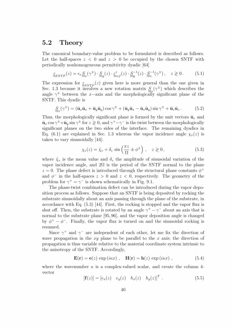
5.2 Theory
The canonical boundary-value problem to be formulated is described as follows.Let the half-spaces z < 0 and z > 0 be occupied by the chosen SNTF withperiodically nonhomogeneous permittivity dyadic [64]
εSNTF
(z) = ϵ0 Sz(γ±) · S
y(z) · ε
ref(z) · S−1
y(z) · S−1
z(γ±) , z ≷ 0 . (5.1)
The expression for εSNTF
(z) given here is more general than the one given inSec. 1.3 because it involves a new rotation matrix S
z(γ±) which describes the
angle γ± between the x−axis and the morphologically significant plane of theSNTF. This dyadic is
Sz(γ±) = (uxux + uyuy) cos γ
± + (uyux − uxuy) sin γ± + uzuz . (5.2)
Thus, the morphologically significant plane is formed by the unit vectors uz andux cos γ
±+uy sin γ± for z ≷ 0, and γ+−γ− is the twist between the morphologically
significant planes on the two sides of the interface. The remaining dyadics inEq. (6.1) are explained in Sec. 1.3 whereas the vapor incidence angle χv(z) istaken to vary sinusoidally [44]:
χv(z) = χv + δv sin(πzΩ
± ϕ±), z ≷ 0 , (5.3)
where χv is the mean value and δv the amplitude of sinusoidal variation of thevapor incidence angle, and 2Ω is the period of the SNTF normal to the planez = 0. The phase defect is introduced through the structural phase constants ϕ+
and ϕ− in the half-spaces z > 0 and z < 0, respectively. The geometry of theproblem for γ+ = γ− is shown schematically in Fig. 9.1.
The phase-twist combination defect can be introduced during the vapor depo-sition process as follows. Suppose that an SNTF is being deposited by rocking thesubstrate sinusoidally about an axis passing through the plane of the substrate, inaccordance with Eq. (5.3) [44]. First, the rocking is stopped and the vapor flux isshut off. Then, the substrate is rotated by an angle γ+ − γ− about an axis that isnormal to the substrate plane [95, 96], and the vapor deposition angle is changedby ϕ+ − ϕ−. Finally, the vapor flux is turned on and the sinusoidal rocking isresumed.
Since γ+ and γ− are independent of each other, let me fix the direction ofwave propagation in the xy plane to be parallel to the x axis; the direction ofpropagation is thus variable relative to the material coordinate system intrinsic tothe anisotropy of the SNTF. Accordingly,
E(r) = e(z) exp (iκx) , H(r) = h(z) exp (iκx) , (5.4)
where the wavenumber κ is a complex-valued scalar, and create the column 4-vector
[f(z)] = [ex(z) ey(z) hx(z) hy(z)]T . (5.5)
40
x, y
z
2Ω
SNTF
Figure 5.1: Schematic illustration of the geometry of the problem, when γ+ = γ−.
Whereas the axial field components ez(z) and hz(z) can be expressed as
κ
ez(z)0
hz(z)0
=[A±(z)
]· [f(z)] , z ≷ 0 , (5.6)
through the 4×4 matrix
[A±(z)
]=
0 0 0 − κ2
ωϵ0
ϵd(z)ϵa(z) ϵb(z)
0 0 0 0
0 κ2
ωµ00 0
0 0 0 0
+κϵd(z) [ϵa(z)− ϵb(z)]
ϵa(z) ϵb(z)sin [χ(z)] cos [χ(z)]
cos γ± sin γ± 0 0
0 0 0 00 0 0 − sin γ±
0 0 0 cos γ±
(5.7)
containing
ϵd(z) = ϵa(z) ϵb(z)/ϵa(z) cos
2 [χ(z)] + ϵb(z) sin2 [χ(z)]
. (5.8)
The column 4-vector [f(z)] satisfies the matrix ordinary differential equation
d
dz[f(z)] = i
[P±(z)
]· [f(z)] , z ≷ 0 , (5.9)
41
where the 4×4 matrix
[P±(z)] = [A±(z)] +
ω
0 0 0 µ0
0 0 −µ0 0ϵ0 [ϵc(z)− ϵd(z)] cos γ
± sin γ± −ϵ0[ϵc(z) cos
2 γ± + ϵd(z) sin2 γ±
]0 0
ϵ0[ϵc(z) sin
2 γ± + ϵd(z) cos2 γ±
]−ϵ0 [ϵc(z)− ϵd(z)] cos γ
± sin γ± 0 0
.
(5.10)
Equation (5.9) requires numerical solution by the piecewise uniform approxi-
mation technique [64]. The ultimate aim is to determine the matrixes[Q+]and[
Q−]that characterize the optical response of one period of the SNTF on either
side of the defect as follows:
[f(±2Ω)] =[Q±]· [f(0±)] . (5.11)
By virtue of the Floquet–Lyapunov theorem [88], the matrixes [Q+] and [Q
−] can
be defined such that[Q±] = exp
±i2Ω[Q±
]. (5.12)
Both [Q±] and [Q±] share the same eigenvectors, and their eigenvalues are also
related as follows. Let [t±](n)
, n ∈ [1, 4], be the eigenvector corresponding to the
nth eigenvalue σ±n of
[Q±]; then, the corresponding eigenvalue α±
n of [Q±] is given
by
α±n = ∓i lnσ
±n
2Ω. (5.13)
The electromagnetic fields of the Dyakonov–Tamm wave must diminish in mag-
nitude as z → ±∞. Therefore, in the half-space z > 0, the eigenvalues of [Q+] are
labeled such that Im[α+1,2
]> 0 and then set [94]
[f (0+)] =[[t+]
(1)[t+]
(2)]·
[A+
1
A+2
], (5.14)
where A+1,2 are unknown scalars; the other two eigenvalues of [Q
+] describe fields
that amplify as z → +∞ and cannot therefore contribute to the Dyakonov–Tammwave. A similar argument for the half-space z < 0 requires us to ensure thatIm[α−1,2
]< 0 and then set [94]
[f (0−)] =[[t−]
(1)[t−]
(2)]·
[A−
1
A−2
], (5.15)
42
where A−1,2 are unknown scalars.
Using Eqs. (5.14) and (5.15) to satisfy the continuity condition [f (0−)] =[f (0+)], a matrix equation is obtained that may be rearranged as
[M ] ·
A+
1
A+2
A−1
A−2
=
0
0
0
0
, (5.16)
where[M ] =
[[t+]
(1)[t+]
(2) − [t−](1) − [t−]
(2)]. (5.17)
For a nontrivial solution, the 4× 4 matrix[M(κ)
]must be singular, so that
det[M(κ)
]= 0 (5.18)
is the dispersion equation for the Dyakonov–Tamm wave.
5.3 Numerical Results and Discussion
The Newton-Raphson technique [89] was implemented on MathematicaTM to solvethe dispersion equation (5.18) for κ. The code for the program is provided inAppendix B.3. The free-space wavelength was fixed at λ0 = 633 nm and the half-period Ω = 200 nm for all calculations reported here. The angles χv and δv weretaken to be 45 and 30, respectively, for all results presented in this chapter. Thephase constants ϕ+ and ϕ− were taken to be 0 and 180, respectively, to generatea 180-phase defect. The angles γ+ and γ− were left as variables in the computerprogram. Moreover, the solutions of the dispersion equation were searched whenκ/k0 > 1.
The matrixes [Q+] and [Q−] were calculated using the piecewise uniform ap-
proximation technique. This technique consists of subdividing each period of theSNTF into a cascade of electrically thin sublayers parallel to the plane z = 0,and assuming the dielectric properties to be spatially uniform in each sublayer. Asufficiently large number N + 1 points z±n = ±2Ω (n/N), n ∈ [0, N ], are definedon each side of the phase-twist combination defect and the matrixes
[W±n] = exp
±i[P±(z±n−1 + z±n
2
)]2Ω
N
, n ∈ [1, N ] , (5.19)
are calculated for a specific value of κ; then
[Q±] ∼= [W±N] · [W±
N−1] · ... · [W±
2] · [W±
1] . (5.20)
43
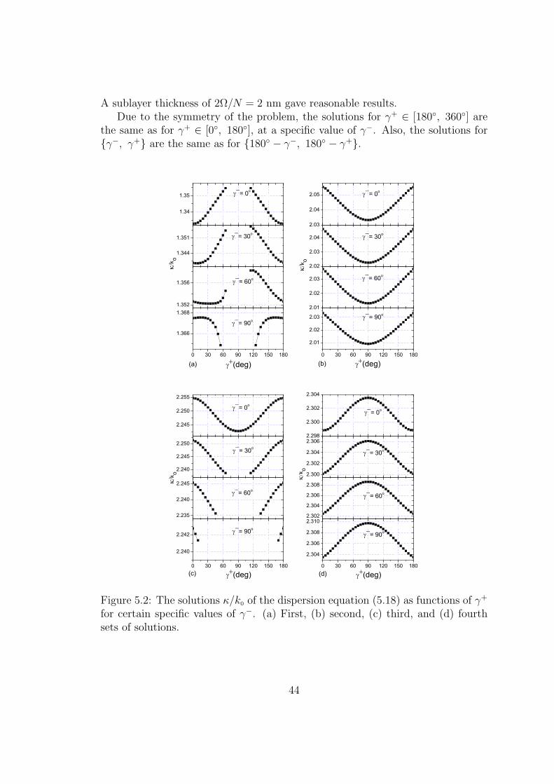
A sublayer thickness of 2Ω/N = 2 nm gave reasonable results.Due to the symmetry of the problem, the solutions for γ+ ∈ [180, 360] are
the same as for γ+ ∈ [0, 180], at a specific value of γ−. Also, the solutions forγ−, γ+ are the same as for 180 − γ−, 180 − γ+.
1.34
1.35
1.344
1.351
1.352
1.356
0 30 60 90 120 150 180
1.366
1.368
(a)
= 0o
= 30o
= 60o
= 90o
(deg)
k o
2.03
2.04
2.05
2.02
2.03
2.04
2.01
2.02
2.03
0 30 60 90 120 150 180
2.01
2.02
2.03
= 0o
(b)
k o
(deg)
= 30o
= 60o
= 90o
2.245
2.250
2.255
2.240
2.245
2.250
2.235
2.240
2.245
0 30 60 90 120 150 180
2.240
2.242
(c)
k o
= 30o
= 0o
(deg)
= 60o
= 90o
2.298
2.300
2.302
2.304
2.300
2.302
2.304
2.306
2.302
2.304
2.306
2.308
0 30 60 90 120 150 180
2.304
2.306
2.308
2.310
= 0o
(d)
= 30o
= 60o
k o
= 90o
(deg)
Figure 5.2: The solutions κ/k0 of the dispersion equation (5.18) as functions of γ+
for certain specific values of γ−. (a) First, (b) second, (c) third, and (d) fourthsets of solutions.
44
5.3.1 Multiple solutions of dispersion equation
Four sets of solutions of the dispersion equation (5.18) are found for γ+ ∈ [0, 180]when γ− was fixed in the interval [0, 90]. Representative results for γ− = 0,30, 60, and 90 are presented in Fig. 5.2 as functions of γ+.
The values of κ/k0 lie between 1.3 and 1.4 in the first set of solutions, presentedin Fig. 5.2(a). Solutions in this set exist
(i) for γ+ ∈ [0, 65] ∪ [115, 180] when γ− = 0, 30 and 60; and
(ii) for γ+ ∈ [0, 55] ∪ [125, 180] when γ− = 90.
It can be noted that solutions do not exist at and in some neighborhood of γ+ =90.
The second set of solutions is given in Fig. 5.2(b). These solutions span thewhole range of γ+ for all values of γ−, and the values of the relative wavenumberκ/k0 lies between 2.0 and 2.06.
The third set of solutions is given in Fig. 5.2(c). The values of the relativewavenumber κ/k0 lie between 2.23 and 2.26. A solution in the third set exists
(i) for γ+ ∈ [0, 180] when γ− = 0,
(ii) for γ+ ∈ [0, 65] ∪ [115, 180] when γ− = 30,
(iii) for γ+ ∈ [0, 45] ∪ [135, 180] when γ− = 60, and
(iv) for γ+ ∈ [0, 15] ∪ [165, 180] when γ− = 90.
The absence of solutions at and in some neighborhood of γ+ = 90, for γ− > 0,is reminiscent of the first set. The γ+-range in which no solution exists widens asγ− increases towards 90.
The solutions in the fourth set are shown in Fig. 5.2(d). Just like in the secondset, the solutions in the fourth set spans the whole range of γ+ for all values ofγ−. The values of the relative wavenumber κ/k0 lie between 2.9 and 2.31.
5.3.2 Decay constants
As mentioned in Sec. 5.2, Dyakonov–Tamm waves must decay away from the in-
terface. To ensure this, the eigenvalues of [Q+] are labeled such that Im
[α+1,2
]> 0,
and the eigenvalues of [Q−] such that Im
[α−1,2
]< 0. To study the decay of
Dyakonov–Tamm waves at distances sufficiently far away from the interface, theconstants that represent the decay after one period (2Ω) of the SNTF are cal-
culated. Since there are two eigenvalues each of [Q+] and [Q
−] that appear in
the representation of a Dyakonov–Tamm wave, there are two decay constants
45

0.7
0.8
0.9
1.0
0.7
0.8
0.9
1.0
0.7
0.8
0.9
1.0
0 30 60 90 120 150 180
0.7
0.8
0.9
1.0
= 0o
= 30o
= 60o
(a)
exp
(-v2)
exp
(-u2)
exp
(-v1)
exp
(-u1)
= 90o
(deg)
0.2
0.3
0.4
0.2
0.3
0.4
0.2
0.3
0.4
0 30 60 90 120 150 180
0.2
0.3
0.4
= 0o
(b) e
xp(-u
2) e
xp(-v
2)(deg)
= 30o
= 60o
e
xp(-u
1) e
xp(-v
1)
= 90o
0.0
0.3
0.6
0.0
0.3
0.6
0.3
0.6
0 30 60 90 120 150 1800.0
0.3
0.6
0.9
(c) (deg)
exp
(-u1)
exp
(-v1)
exp
(-u2)
exp
(-v2)
= 0o
= 30o
= 60o
= 90o
0.03
0.06
0.09
0.12
0.03
0.06
0.09
0.03
0.06
0.09
0.12
0 30 60 90 120 150 180
0.03
0.06
0.09
= 0o
(deg)
(d)
exp
(-v1)
exp
(-v2)
exp
(-u2)
= 30o
= 60o
exp
(-u1)
= 90o
Figure 5.3: The decay constants exp(−u1), exp(−u2), exp(−v1), and exp(−v2) forthe (a) first, (b) second, (c) third, and (d) fourth set of solutions in Fig. 5.2.
on either side of the interface. Four decay constants are defined [65, 67, 68] asexp(−u1), exp(−u2), exp(−v1), and exp(−v2), where u1,2 = 2Ω · Im
[α+1,2
]and
v1,2 = −2Ω · Im[α−1,2
]. The decay constants for all solutions of the dispersion
equation provided in Fig. 5.2 are presented in Fig. 5.3. The degree of localizationof the Dyakonov–Tamm wave to the defect interface depends on the value of thedecay constants. The Dyakonov–Tamm wave is strongly localized if the decay
46
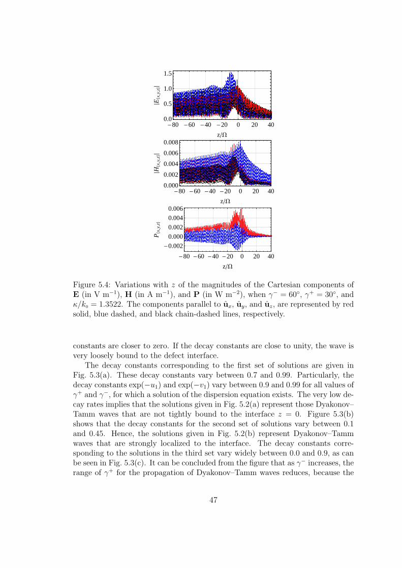
-80 -60 -40 -20 0 20 400.0
0.5
1.0
1.5
zW
ÈE8x
,y,z<È
-80 -60 -40 -20 0 20 400.000
0.002
0.004
0.006
0.008
zW
ÈH8x
,y,z<È
-80 -60 -40 -20 0 20 40
-0.002
0.000
0.002
0.004
0.006
zW
P8x
,y,z<
Figure 5.4: Variations with z of the magnitudes of the Cartesian components ofE (in V m−1), H (in A m−1), and P (in W m−2), when γ− = 60, γ+ = 30, andκ/k0 = 1.3522. The components parallel to ux, uy, and uz, are represented by redsolid, blue dashed, and black chain-dashed lines, respectively.
constants are closer to zero. If the decay constants are close to unity, the wave isvery loosely bound to the defect interface.
The decay constants corresponding to the first set of solutions are given inFig. 5.3(a). These decay constants vary between 0.7 and 0.99. Particularly, thedecay constants exp(−u1) and exp(−v1) vary between 0.9 and 0.99 for all values ofγ+ and γ−, for which a solution of the dispersion equation exists. The very low de-cay rates implies that the solutions given in Fig. 5.2(a) represent those Dyakonov–Tamm waves that are not tightly bound to the interface z = 0. Figure 5.3(b)shows that the decay constants for the second set of solutions vary between 0.1and 0.45. Hence, the solutions given in Fig. 5.2(b) represent Dyakonov–Tammwaves that are strongly localized to the interface. The decay constants corre-sponding to the solutions in the third set vary widely between 0.0 and 0.9, as canbe seen in Fig. 5.3(c). It can be concluded from the figure that as γ− increases, therange of γ+ for the propagation of Dyakonov–Tamm waves reduces, because the
47

-4 -2 0 2 40.0
0.5
1.0
1.5
2.0
2.5
zW
ÈE8x
,y,z<È
-4 -2 0 2 40.0000.0020.0040.0060.0080.0100.0120.014
zW
ÈH8x
,y,z<È
-4 -2 0 2 40.0000.0050.0100.0150.0200.025
zW
P8x
,y,z<
Figure 5.5: Same as Fig. 5.4 except that κ/k0 = 2.02646.
decay constant exp(−v1) grows rapidly as γ+ either increases from 0 or decreasesfrom 180. The growth rate of exp(−v1) is higher at a higher value of γ−. Finally,the decay constants for the solutions in Fig. 5.2(d) are given in Fig. 5.3(d). Thesedecay constants lie between 0.0 and 0.12. Evidently, the Dyakonov–Tamm wavescorresponding to the solutions in Fig. 5.2(d) are the most tightly bound to thephase-twist combination defect.
5.3.3 Spatial profiles
In order to further illustrate the anatomy of Dyakonov–Tamm waves, the spatialprofiles of the electric field phasor E, the magnetic field phasor H and the time-averaged Poynting vector P = (1/2)Re (E×H∗) are computed for all four solu-tions of the dispersion equation (5.18) when γ− = 60 and γ+ = 30. The coeffi-cients A+
2 , A−1 , and A
−2 were computed using Eq. (5.16) after setting A+
1 = 1 V m−1
therein. Spatial profiles of the four solutions are presented in Figs. 5.4–5.7.The spatial profiles for the first solution (κ/k0 = 1.3522) are presented in
Fig. 5.4. The decay is faster in the half-space z > 0 relative to the half-space z < 0,
48

-4 -2 0 2 40
1
2
3
4
5
zW
ÈE8x
,y,z<È
-4 -2 0 2 40.0000.0050.0100.0150.0200.0250.030
zW
ÈH8x
,y,z<È
-4 -2 0 2 40.00
0.02
0.04
0.06
0.08
zW
P8x
,y,z<
Figure 5.6: Same as Fig. 5.4 except that κ/k0 = 2.2395.
as also signified by the following values of the four decay constants: exp(−u1) =0.94 and exp(−u2) = 0.74 for z > 0, exp(−v1) = 0.99 and exp(−v2) = 0.84 forz < 0. The spatial profiles (not shown) and decay constants for other solutions inFig. 5.2(a) show qualitatively similar disparities, thereby permitting the conclusionthat the Dyakonov–Tamm waves from the first set of solutions are quite looselybound to the phase-twist combination defect.
In Fig. 5.5, the spatial profiles of the magnitudes of the components of E, H,and P are given for the second solution (κ/k0 = 2.02646). The Dyakonov–Tammwave is confined within one period of the SNTF on either side of the defect. Theasymmetry in the spatial profiles is due to the asymmetry of the arrangement ofthe morphologically significant planes of the SNTF on either side of the interface.The same observations and conclusions hold for the spatial profiles depicted inFig. 5.6 for the third solution (κ/k0 = 2.2395) as well as for the spatial profilesdepicted in Fig. 5.7 for the fourth solution (κ/k0 = 2.3050). Thus, it can beconcluded that all of these three Dyakonov–Tamm waves are tightly bound to thephase-twist combination defect.
49

-4 -2 0 2 40.0
0.5
1.0
1.5
zW
ÈE8x
,y,z<È
-4 -2 0 2 40.0000.0020.0040.0060.0080.010
zW
ÈH8x
,y,z<È
-4 -2 0 2 40.0000.0020.0040.0060.0080.010
zW
P8x
,y,z<
Figure 5.7: Same as Fig. 5.4 except that κ/k0 = 2.3050.
5.4 Concluding Remarks
The canonical boundary-value problem of surface-wave propagation guided by aphase-twist combination defect in a periodically nonhomogeneous SNTF is formu-lated and numerically solved . A structural phase difference ϕ+ − ϕ− was fixed at180 while the twist γ+−γ− between the morphologically significant planes of theSNTF on either side of the combination defect was kept variable. The direction ofpropagation (in the plane of the defect interface) was varied by choosing variousvalues of γ+ and γ−. It was found that
(i) multiple Dyakonov–Tamm waves can propagate, guided by the combinationdefect, depending upon the twist and the direction of propagation, withdifferent phase speeds and degrees of localization to the interface; and
(ii) the most strongly localized Dyakonov–Tamm waves are confined within onestructural period of the SNTF on either side of the defect interface.
Conclusion (ii) is in contrast to the results obtained for Dyakonov–Tamm wavesguided by a twist defect in a chiral STF, where Dyakonov–Tamm waves are at
50

best confined within two structural periods. As the chiral STFs of Gao et al. [65,67] and the SNTFs in this chapter are taken to be made of the same material(titanium oxide), and the periods differ by just 1.5%, the difference in the highestdegrees of localization must be attributed to the differences in the morphologicaldimensionality of the two types of STFs:
(i) the morphology of a chiral STF requires a three-dimensional curve for itsdescription, whereas
(ii) that of an SNTF only a two-dimensional curve.
Let me note that only Tamm waves will be guided by the structural defect ifthe partnering dielectric materials of this chapter were to be made isotropic, ashas been shown in Appendix A.
51

Chapter 6
SPP Waves Guided by a MetalSlab in an SNTF ‡
6.1 Introduction
The possibility of multiple SPP waves localized to the single interface of a metaland a periodically nonhomogeneous SNTF has been demonstrated both theoret-ically in Ch. 2 and elsewhere [70, 71], and experimentally [44]. Also, SPP-wavepropagation along the interface of a metal and a chiral STF has been shown boththeoretically [26] and experimentally [43] to admit more than one type of SPPwaves. A further increase in the number of SPP waves would require the use ofmultiple parallel metal/dielectric interfaces, which is already established well withisotropic dielectric materials [113–115]. Pursuing this line of thinking, the canoni-cal problem of wave propagation guided by a sufficiently thin metallic slab insertedin a periodically nonhomogeneous SNTF that completely occupies the half-spaceson both sides of the slab, is undertaken in this chapter. In Sec. 6.2, the theo-retical formulation of the canonical boundary-value problem is presented, wherea dispersion equation is obtained. Representative numerical results are discussedin Sec. 6.3 for a metallic slab made of bulk aluminum and for an electron-beamevaporated thin film. Finally, concluding remarks are given in Sec. 6.4. It must benoted that the canonical problem treated here underlies pragmatic configurationsto actually excite and exploit SPP waves [35,116,117].
.
‡This chapter is based on: (i) M. Faryad and A. Lakhtakia, “Surface plasmon-polariton wavepropagation guided by a metal slab in a sculptured nematic thin film,” J. Opt. (United Kingdom)12, 085102 (2010); (ii) M. Faryad and A. Lakhtakia, “Multiple surface-plasmon-polariton waveslocalized to a metallic defect layer in a sculptured nematic thin film,” Phys. Status Solidi—RapidRes. Lett. 4, 265–267 (2010); and (iii) M. Faryad and A. Lakhtakia, “Coupled surface-plasmon-polariton waves in a sculptured nematic thin film with a metallic defect layer,” Proc. SPIE7766, 77660L (2010).
52

6.2 Canonical Boundary-Value Problem
Suppose that the region L− ≤ z ≤ L+ is occupied by an isotropic and homogeneousmetal with complex-valued relative permittivity scalar ϵm. The thickness of themetal slab is denoted by Lmet = L+ − L−.
The regions z ≷ L± are occupied by the chosen SNTF with periodically non-homogeneous permittivity dyadic [70, 71]
ϵSNTF
(z) = ϵ0 Sz(γ±) · S
y(z) · ϵo
ref(z) · S−1
y(z) · S−1
z(γ±) , z ≷ L± , (6.1)
where the locally orthorhombic symmetry is expressed through the diagonal dyadic
ϵoref
(z) = ϵa(z) uzuz + ϵb(z) uxux + ϵc(z) uyuy (6.2)
and the local tilt dyadic
Sy(z) = (uxux + uzuz) cos [χ(z)] + (uzux − uxuz) sin [χ(z)] + uyuy (6.3)
expresses nematicity. Both the relative permittivity scalars ϵa,b,c(z) and the tiltangle χ(z) are supposed to have been nano-engineered by a periodic variation of thedirection of the vapor flux during fabrication by physical vapor deposition [1,44].This periodic variation is captured by the vapor incidence angle [44]
χv(z) = χv ± δv sin
[π(z − L±)
Ω
], z ≷ L± , (6.4)
that varies sinusoidally with z, where χv is the mean value and δv the amplitudeof the sinusoidal variation of the vapor incidence angle, and 2Ω is the period ofthe SNTF normal to the interface. The third dyadic in Eq. (6.1) was chosen as
Sz(γ±) = (uxux + uyuy) cos γ
± + (uyux − uxuy) sin γ± + uzuz , (6.5)
so that plane formed by the unit vectors uz and ux cos γ± + uy sin γ
± is the mor-phologically significant plane for z ≷ L±. Thus, there is sufficient flexibility in theformulation with respect to the twist γ+ − γ− of the two morphologically signif-icant planes. The geometry of the canonical problem is shown schematically inFig. 6.1.
Without loss of generality, let me choose the direction of SPP-wave propagationin the xy plane to be parallel to the x axis. Accordingly,
E(r) = e(z) exp (iκx)H(r) = h(z) exp (iκx)
, (6.6)
where κ is a complex-valued scalar.
53

x, y
z
2Ω
SNTF
metal slab
Lmet
Figure 6.1: Schematic illustration of the geometry of the canonical boundary-valueproblem for γ+ = γ−.
The axial field components ez(z) and hz(z) can be expressed in terms of thecolumn 4-vector
[f(z)] = [ex(z) ey(z) hx(z) hy(z)]T (6.7)
via
κ
ez(z)0
hz(z)0
=
[A±(z)
]· [f(z)] , z ≷ L± ,[
Amet(z)]· [f(z)] , z ∈ (L−, L+) ,
(6.8)
where one 4×4 matrix
[A±(z)
]=
0 0 0 − κ2
ωϵ0
ϵd(z)ϵa(z) ϵb(z)
0 0 0 0
0 κ2
ωµ00 0
0 0 0 0
+κϵd(z) [ϵa(z)− ϵb(z)]
ϵa(z) ϵb(z)sin [χ(z)] cos [χ(z)]
cos γ± sin γ± 0 0
0 0 0 00 0 0 − sin γ±
0 0 0 cos γ±
involves the auxiliary quantity
ϵd(z) = ϵa(z) ϵb(z)/ϵa(z) cos
2 [χ(z)] + ϵb(z) sin2 [χ(z)]
,
and the other 4×4 matrix
[Amet(z)
]=
0 0 0 − κ2
ωϵ0ϵm
0 0 0 0
0 κ2
ωµ00 0
0 0 0 0
.
54

The column 4-vector [f(z)] satisfies the matrix differential equations
d
dz[f(z)] = i
[P±(z)
]· [f(z)] , z ≷ L± , (6.9)
andd
dz[f(z)] = i
[Pmet(z)
]· [f(z)] , z ∈ (L−, L+) , (6.10)
where the 4×4 matrixes[P±(z)
]=[A±(z)
]+
ω
0 0 0 µ0
0 0 −µ0 0ϵ0 [ϵc(z)− ϵd(z)] cos γ
± sin γ± −ϵ0[ϵc(z) cos
2 γ± + ϵd(z) sin2 γ±
]0 0
ϵ0[ϵc(z) sin
2 γ± + ϵd(z) cos2 γ±
]−ϵ0 [ϵc(z)− ϵd(z)] cos γ
± sin γ± 0 0
and
[Pmet(z)
]=[Amet(z)
]+ ω
0 0 0 µ0
0 0 −µ0 00 −ϵ0ϵm 0 0
ϵ0ϵm 0 0 0
.
Equation (6.10) can be solved straightforwardly to yield
[f(L+)] = expi[Pmet
](L+ − L−)
· [f(L−] . (6.11)
Equation (6.9) requires numerical solution by the piecewise uniform approximation
technique [64]. The ultimate aim is to determine the matrixes[Q±]that appear
in the relations[f(L± ± 2Ω)] =
[Q±]· [f(L±)] (6.12)
to characterize the optical response of one period of the SNTF on either side ofthe metal slab. Basically, this technique consists of subdividing each period ofthe SNTF into a cascade of electrically thin sublayers parallel to the plane z = 0,and assuming the dielectric properties to be spatially uniform in each sublayer.A sufficiently large number N + 1 points z±n = L± ± 2Ω (n/N), n ∈ [0, N ], aredefined on each side of the metal slab and the matrixes
[W±n] = exp
±i[P±(z±n−1 + z±n
2
)]2Ω
N
, n ∈ [1, N ] , (6.13)
are calculated for a specific value of κ; then
[Q±] ∼= [W±N] · [W±
N−1] · ... · [W±
2] · [W±
1] . (6.14)
55

A sublayer thickness 2Ω/N = 2 nm was adequate for the results reported inSec. 6.3.
By virtue of the Floquet–Lyapunov theorem [88], the matrixes [Q±] can be
defined such that[Q±] = exp
±i2Ω[Q±
]. (6.15)
Both [Q±] and [Q±] share the same eigenvectors, and their eigenvalues are also
related as follows. Let [t±](n)
, n ∈ [1, 4], be the eigenvector corresponding to the
nth eigenvalue σ±n of
[Q±]; then, the corresponding eigenvalue α±
n of [Q±] is given
by
α±n = ∓i lnσ
±n
2Ω. (6.16)
The electromagnetic fields of the SPP wave must diminish in magnitude as
z → ±∞. Therefore, in the half-space z > L+, the eigenvalues of [Q+] are labeled
such that Im[α+1,2
]> 0 and then set
[f (L+)] =[[t+]
(1)[t+]
(2)]·
[A+
1
A+2
], (6.17)
where A+1,2 are unknown scalars; the other two eigenvalues of [Q
+] describe fields
that amplify as z → +∞ and cannot therefore contribute to the SPP wave. Asimilar argument for the half-space z < L− requires us to ensure that Im
[α−1,2
]< 0
and then to set
[f (L−)] =[[t−]
(1)[t−]
(2)]·
[A−
1
A−2
], (6.18)
where A−1,2 are unknown scalars.
Combining Eqs. (6.11), (6.17), and (6.18) to ensure the continuity of the tan-gential components of the electric and magnetic fields across each of the two met-al/SNTF interfaces, a matrix equation can be obtained:
[[t+]
(1)[t+]
(2)]·
[A+
1
A+2
]= exp
i[P s](L+ − L−)
·[[t−]
(1)[t−]
(2)]·
[A−
1
A−2
],
(6.19)which may be rearranged as
[M(κ)] ·
A+
1
A+2
A−1
A−2
=
0
0
0
0
. (6.20)
56

For a nontrivial solution, the 4× 4 matrix[M(κ)
]must be singular, so that
det[M(κ)
]= 0 (6.21)
is the dispersion equation for SPP-wave propagation.
6.3 Numerical Results and Discussion
A MathematicaTM program was written and implemented to solve (6.21) to obtainκ for specific values of γ+ and γ−. The code for the program is provided inAppendix B.4. The free-space wavelength was fixed at λ0 = 633 nm and the half-period Ω = 200 nm for all calculations. The angles χv and δv were taken to be45 and 30, respectively, for all results presented in this chapter. The dispersionequation (6.21) was solved using the Newton-Raphson technique [89] for a defectlayer made of bulk aluminum and electron-beam evaporated aluminum thin film,and the solutions were searched when Re [κ/k0] > 1.
6.3.1 Bulk aluminum defect layer
The dispersion equation for bulk aluminum defect layer was solved for three dif-ferent values of the twist between the morphologically significant planes on eitherside of the metal slab;
(i) γ− = γ+,
(ii) γ− = γ+ + 90, and
(iii) γ− = γ+ + 45,
while γ+ was kept as a variable. For each choice, the boundaries of the metalslab were taken to be at L± = ±7.5, ±12.5, ±25, or ±45 nm. These selectionsadequately represent the results of my investigation.
The metal was taken to be bulk aluminum (ϵm = −56 + 21i). The skin depth
of aluminum at the chosen wavelength is ∆met =Im[k0
√ϵm]−1
= 13.24 nm, aquantity of interest in relation to the thickness of the metal slab.
γ− = γ+
Let me begin with the case when the morphologically significant planes of theSNTF on both sides of the metal slab are aligned with each other and make anangle γ− = γ+ with respect to the direction of SPP-wave propagation in the xyplane.
The real and imaginary parts of κ/k0 which satisfies Eq. (6.21) are presentedin Fig. 6.2 as functions of γ+ ∈ [0, 90]; by virtue of symmetry, the solutions
57

0 15 30 45 60 75 901.85
1.90
1.95
2.00
2.05
2.10
2.4
2.5
2.6
2.7
0 15 30 45 60 75 900.000
0.005
0.010
0.015
0.020
0.025
0.180
0.185
0.190
Re
[k o
]
(deg)
Im [
k o]
(deg)(a)0 15 30 45 60 75 90
1.85
1.90
1.95
2.00
2.05
2.10
2.425
2.450
2.475
0 15 30 45 60 75 900.0000
0.0025
0.0050
0.0075
0.03
0.04
0.05
Re
[/k
o]
+(deg)
Im [
/ko]
+(deg)(c)
0 15 30 45 60 75 901.8
1.9
2.0
2.1
2.4
2.5
2.6
0 15 30 45 60 75 900.000
0.005
0.010
0.015
0.020
0.09
0.10
Re
[/k
o]
(deg) (b)
Im [
/ko]
+(deg)0 15 30 45 60 75 90
1.85
1.90
1.95
2.00
2.05
2.10
2.40
2.45
2.50
0 15 30 45 60 75 900.0000
0.0025
0.0050
0.0075
0.04
0.05
Re
[/k
o]
+(deg)
Im [
/ko]
+(deg)(d)
Figure 6.2: Variation of real and imaginary parts of κ/k0 with γ+, when γ− = γ+.
(a) L± = ±7.5 nm, (b) L± = ±12.5 nm, (c) L± = ±25 nm, and (d) L± = ±45 nm.
for 180 + γ+ and 360 − γ+ are the same as for γ+. For the thinnest metal slab(L± = ±7.5 nm), the solutions are organized in five branches which span the entirerange of γ+. As the metal slab thickens to 25 nm (L± = ±12.5 nm), the numberof branches does not change, but only four of those branches span the entire rangeof γ+ and one is confined to γ+ ∈ [0, 49]. Further thickening of the metal slab to50 nm (L± = ±25 nm) leads to five values of κ satisfying the dispersion equationonly in the range γ+ ∈ [0, 35], four in the range γ+ ∈ (35, 37], and three in therange γ+ ∈ (37, 90]. Finally, for a 90-nm thick metal slab (L± = ±45 nm) onlythree solutions exist for γ ∈ [0, 36] and two for γ ∈ (36, 90], these solutionsbeing the same as for a single metal/SNTF interface as given in Ch. 2. It canbe concluded that, as the thickness of the metal slab is increased, the couplingbetween two metal/SNTF interfaces z = L− and z = L+ decreases; ultimately,the two interfaces decouple from each other when the thickness Lmet significantlyexceeds twice the skin depth ∆met in the metal.
The solutions in Fig. 6.2 can be categorized into three sets. The first setcomprises those solutions for which Re[κ/k0] lies between 2.3 and 2.7. This sethas two branches when the metal slab is 15-nm thick, both branches spanning
58

(a)
-1.0 -0.5 0.0 0.5 1.0
0.000
0.002
0.004
0.006
0.008
0.010
zW
P8x
,y,z<
(d)
-1.5 -1.0 -0.5 0.0 0.5 1.0 1.5
0.000
0.002
0.004
0.006
0.008
zW
P8x
,y,z<
(b)
-4 -2 0 2 40.00
0.01
0.02
0.03
0.04
0.05
zW
P8x
,y,z<
(e)
-4 -2 0 2 40.000.050.100.150.200.250.300.35
zW
P8x
,y,z<
(c)
-6 -4 -2 0 2 4 6-0.002
0.0000.0020.0040.0060.0080.0100.012
zW
P8x
,y,z<
(f)
-6 -4 -2 0 2 4 6
0.000
0.002
0.004
0.006
0.008
0.010
zW
P8x
,y,z<
Figure 6.3: Variation of the Cartesian components of the time-averaged Poyntingvector P(x, z) (in W m−2) along the z axis when x = 0, L± = ±7.5 nm, andγ− = γ+. (a-c) γ+ = 0, and (d-f) γ+ = 25. (a) κ/k0 = 2.6387+i0.1839, (b) κ/k0 =2.0964 + i0.009997, (c) κ/k0 = 1.9048 + i0.02696, (d) κ/k0 = 2.6399 + i0.1848, (e)κ/k0 = 2.09285 + i0.00988, and (f) κ/k0 = 1.9103 + i0.02405. The x-, y- andz-directed components of P(x, z) are represented by solid red, dashed blue, andchain-dashed black lines, respectively.
the entire range of γ+. As the thickness Lmet increases, the two branches comecloser to each other and eventually merge completely. The second set comprisessolutions for which Re [κ/k0] lies between 2.05 and 2.1. It also has two brancheswhen Lmet = 15 nm, both branches coalescing into one branch as the thicknessincreases. Complete merger of the two branches of the first set occurs at a value ofLmet smaller than that for the two branches of the first set. Regardless of the valueof Lmet, solutions in the second set can be found over the entire range of γ+. Thethird set consists of solutions lying on just one branch (1.85 < Re [κ/k0] < 1.95),but the maximum value of γ+ on this branch decreases rapidly from 90 as Lmet
increases from 15 nm.The foregoing categorization is also meaningful as the spatial profiles of the
fields are very similar for both solutions (for a specific value of γ+) in the first twosets. The same remark can be made for the spatial profiles of the time-averaged
59

(a)
-1.5 -1.0 -0.5 0.0 0.5 1.0 1.5
0.0000.0050.0100.0150.0200.0250.0300.035
zW
P8x
,y,z<
(d)
-1.5 -1.0 -0.5 0.0 0.5 1.0 1.5
0.000
0.005
0.010
0.015
zW
P8x
,y,z<
(b)
-4 -2 0 2 40.00
0.05
0.10
0.15
zW
P8x
,y,z<
(e)
-4 -2 0 2 40.00
0.05
0.10
0.15
0.20
zW
P8x
,y,z<
(c)
-10 -5 0 5 10
0.0000.0050.0100.0150.0200.0250.0300.035
zW
P8x
,y,z<
(f)
-15 -10 -5 0 5 10 15
0.000
0.002
0.004
0.006
0.008
0.010
0.012
zW
P8x
,y,z<
Figure 6.4: Same as Fig. 6.3 except for L± = ±45 nm. (a) κ/k0 = 2.4549 +i0.04173, (b) κ/k0 = 2.08034+ i0.003574, (c) κ/k0 = 1.8683+ i0.00734, (d) κ/k0 =2.4557+ i0.04181, (e) κ/k0 = 2.0773+ i0.00363, and (f) κ/k0 = 1.8830+ i0.00413.
Poynting vector
P(x, z) =1
2Re [E(x, z)×H∗(x, z)] . (6.22)
Representative plots of P(0, z) against z are presented in Figs. 6.3 and 6.4 forcombinations of (i) three values of κ, one from each set, and (ii) two values of γ+.Whereas γ+ = 0 was chosen because it represents the propagation of SPP wavesin the morphologically significant plane of the SNTF on either side of the metalslab, γ+ = 25 was chosen for the direction of SPP-wave propagation oblique tothat plane.
Figure 6.3 shows the spatial profiles of P(0, z) for L± = ±7.5 nm and sixselected values of κ. In order to determine these profiles, first A+
1 was set equalto unity and then the remaining coefficients were found using Eq. (6.20); theexception is Figure 6.3(b), for which A+
2 = 1 was set and the remaining coefficientswere found using Eq. (6.20). The spatial profiles shown allow us to conc4lude that
(i) the SPP waves are bound strongly to both metal/SNTF interfaces, and
(ii) the power density mostly resides in the SNTF.
60
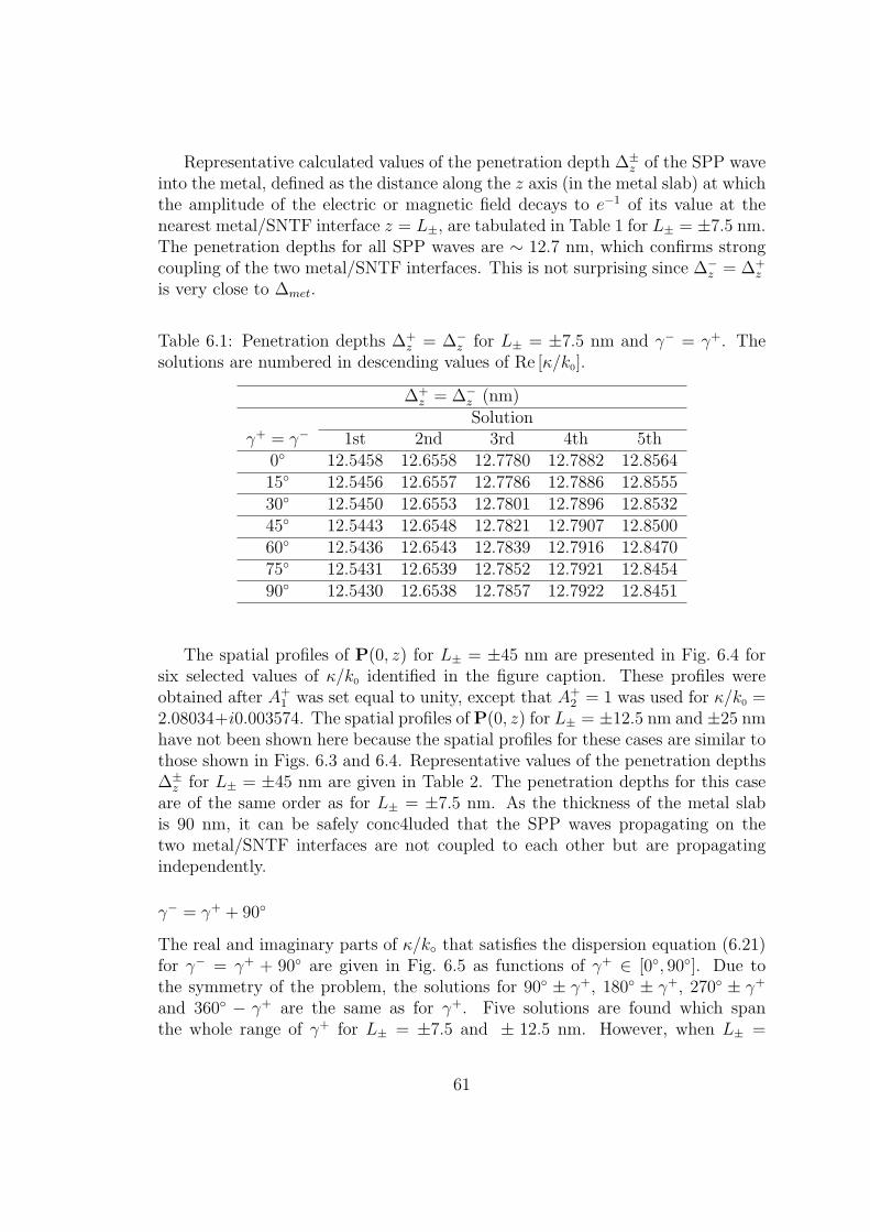
Representative calculated values of the penetration depth ∆±z of the SPP wave
into the metal, defined as the distance along the z axis (in the metal slab) at whichthe amplitude of the electric or magnetic field decays to e−1 of its value at thenearest metal/SNTF interface z = L±, are tabulated in Table 1 for L± = ±7.5 nm.The penetration depths for all SPP waves are ∼ 12.7 nm, which confirms strongcoupling of the two metal/SNTF interfaces. This is not surprising since ∆−
z = ∆+z
is very close to ∆met.
Table 6.1: Penetration depths ∆+z = ∆−
z for L± = ±7.5 nm and γ− = γ+. Thesolutions are numbered in descending values of Re [κ/k0].
∆+z = ∆−
z (nm)Solution
γ+ = γ− 1st 2nd 3rd 4th 5th0 12.5458 12.6558 12.7780 12.7882 12.856415 12.5456 12.6557 12.7786 12.7886 12.855530 12.5450 12.6553 12.7801 12.7896 12.853245 12.5443 12.6548 12.7821 12.7907 12.850060 12.5436 12.6543 12.7839 12.7916 12.847075 12.5431 12.6539 12.7852 12.7921 12.845490 12.5430 12.6538 12.7857 12.7922 12.8451
The spatial profiles of P(0, z) for L± = ±45 nm are presented in Fig. 6.4 forsix selected values of κ/k0 identified in the figure caption. These profiles wereobtained after A+
1 was set equal to unity, except that A+2 = 1 was used for κ/k0 =
2.08034+i0.003574. The spatial profiles of P(0, z) for L± = ±12.5 nm and ±25 nmhave not been shown here because the spatial profiles for these cases are similar tothose shown in Figs. 6.3 and 6.4. Representative values of the penetration depths∆±
z for L± = ±45 nm are given in Table 2. The penetration depths for this caseare of the same order as for L± = ±7.5 nm. As the thickness of the metal slabis 90 nm, it can be safely conc4luded that the SPP waves propagating on thetwo metal/SNTF interfaces are not coupled to each other but are propagatingindependently.
γ− = γ+ + 90
The real and imaginary parts of κ/k that satisfies the dispersion equation (6.21)for γ− = γ+ + 90 are given in Fig. 6.5 as functions of γ+ ∈ [0, 90]. Due tothe symmetry of the problem, the solutions for 90 ± γ+, 180 ± γ+, 270 ± γ+
and 360 − γ+ are the same as for γ+. Five solutions are found which spanthe whole range of γ+ for L± = ±7.5 and ± 12.5 nm. However, when L± =
61

Table 6.2: Penetration depths ∆+z = ∆−
z for L± = ±45 nm and γ− = γ+. Thesolutions are numbered in descending values of Re [κ/k0].
∆+z = ∆−
z (nm)Solution
γ+ = γ− 1st 2nd 3rd0 12.6206 12.7843 12.869115 12.6205 12.7848 12.866930 12.6201 12.7860 12.860845 12.6196 12.787760 12.6192 12.789175 12.6188 12.790190 12.6187 12.7904
0 15 30 45 60 75 901.9
2.0
2.1
2.2
2.3
2.4
2.5
2.6
0 15 30 45 60 75 900.000
0.005
0.010
0.015
0.17
0.18
0.19
Re
[k o
]
(deg)
Im [
k o]
(deg)(a)0 15 30 45 60 75 90
1.85
1.90
1.95
2.00
2.05
2.10
2.44
2.46
0 15 30 45 60 75 900.000
0.002
0.004
0.006
0.0080.03
0.04
0.05
R
e [
k o]
(deg) (c)
Im [
k o]
(deg)
0 15 30 45 60 75 901.8
2.0
2.2
2.4
2.6
0 15 30 45 60 75 900.000
0.005
0.010
0.015
0.08
0.09
Re
[k o
]
(deg)
Im [
k o]
(deg)(b)0 15 30 45 60 75 90
1.85
1.90
1.95
2.00
2.05
2.102.40
2.45
0 15 30 45 60 75 900.000
0.002
0.004
0.006
0.008
0.040
0.045
Re
[k o
]
(deg)
Im [
k o]
(deg)(d)
Figure 6.5: Same as Fig. 6.2 except that γ− = γ+ + 90.
±25 and ± 45 nm, only four solutions exist for γ ∈ (37, 53), but five for othervalues of γ+ ∈ [0, 37] ∪ [53, 90].
62
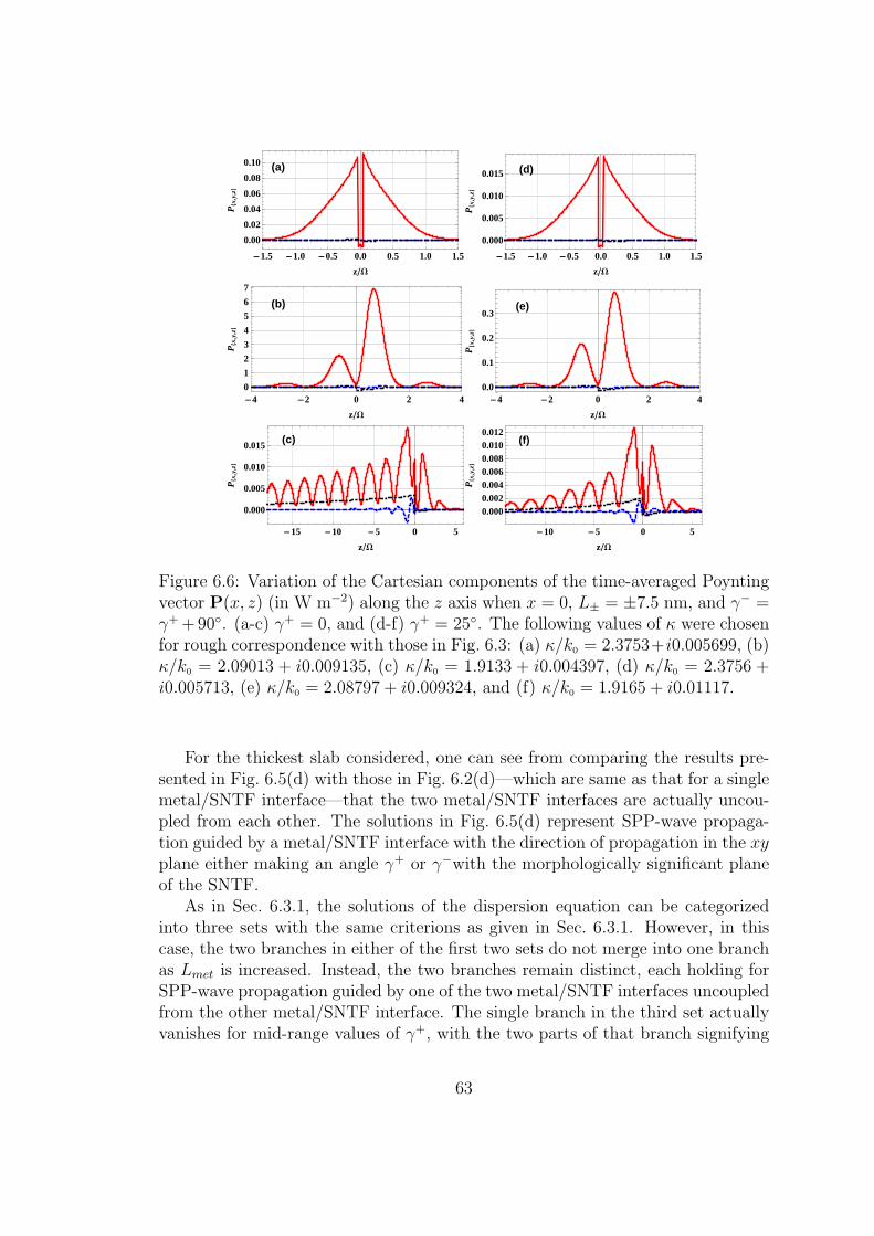
(a)
-1.5 -1.0 -0.5 0.0 0.5 1.0 1.5
0.00
0.02
0.04
0.06
0.08
0.10
zW
P8x
,y,z<
(d)
-1.5 -1.0 -0.5 0.0 0.5 1.0 1.5
0.000
0.005
0.010
0.015
zW
P8x
,y,z<
(b)
-4 -2 0 2 40
1
2
3
4
5
6
7
zW
P8x
,y,z<
(e)
-4 -2 0 2 40.0
0.1
0.2
0.3
zW
P8x
,y,z<
(c)
-15 -10 -5 0 5
0.000
0.005
0.010
0.015
zW
P8x
,y,z<
(f)
-10 -5 0 5
0.0000.0020.0040.0060.0080.0100.012
zW
P8x
,y,z<
Figure 6.6: Variation of the Cartesian components of the time-averaged Poyntingvector P(x, z) (in W m−2) along the z axis when x = 0, L± = ±7.5 nm, and γ− =γ++90. (a-c) γ+ = 0, and (d-f) γ+ = 25. The following values of κ were chosenfor rough correspondence with those in Fig. 6.3: (a) κ/k0 = 2.3753+i0.005699, (b)κ/k0 = 2.09013 + i0.009135, (c) κ/k0 = 1.9133 + i0.004397, (d) κ/k0 = 2.3756 +i0.005713, (e) κ/k0 = 2.08797 + i0.009324, and (f) κ/k0 = 1.9165 + i0.01117.
For the thickest slab considered, one can see from comparing the results pre-sented in Fig. 6.5(d) with those in Fig. 6.2(d)—which are same as that for a singlemetal/SNTF interface—that the two metal/SNTF interfaces are actually uncou-pled from each other. The solutions in Fig. 6.5(d) represent SPP-wave propaga-tion guided by a metal/SNTF interface with the direction of propagation in the xyplane either making an angle γ+ or γ−with the morphologically significant planeof the SNTF.
As in Sec. 6.3.1, the solutions of the dispersion equation can be categorizedinto three sets with the same criterions as given in Sec. 6.3.1. However, in thiscase, the two branches in either of the first two sets do not merge into one branchas Lmet is increased. Instead, the two branches remain distinct, each holding forSPP-wave propagation guided by one of the two metal/SNTF interfaces uncoupledfrom the other metal/SNTF interface. The single branch in the third set actuallyvanishes for mid-range values of γ+, with the two parts of that branch signifying
63
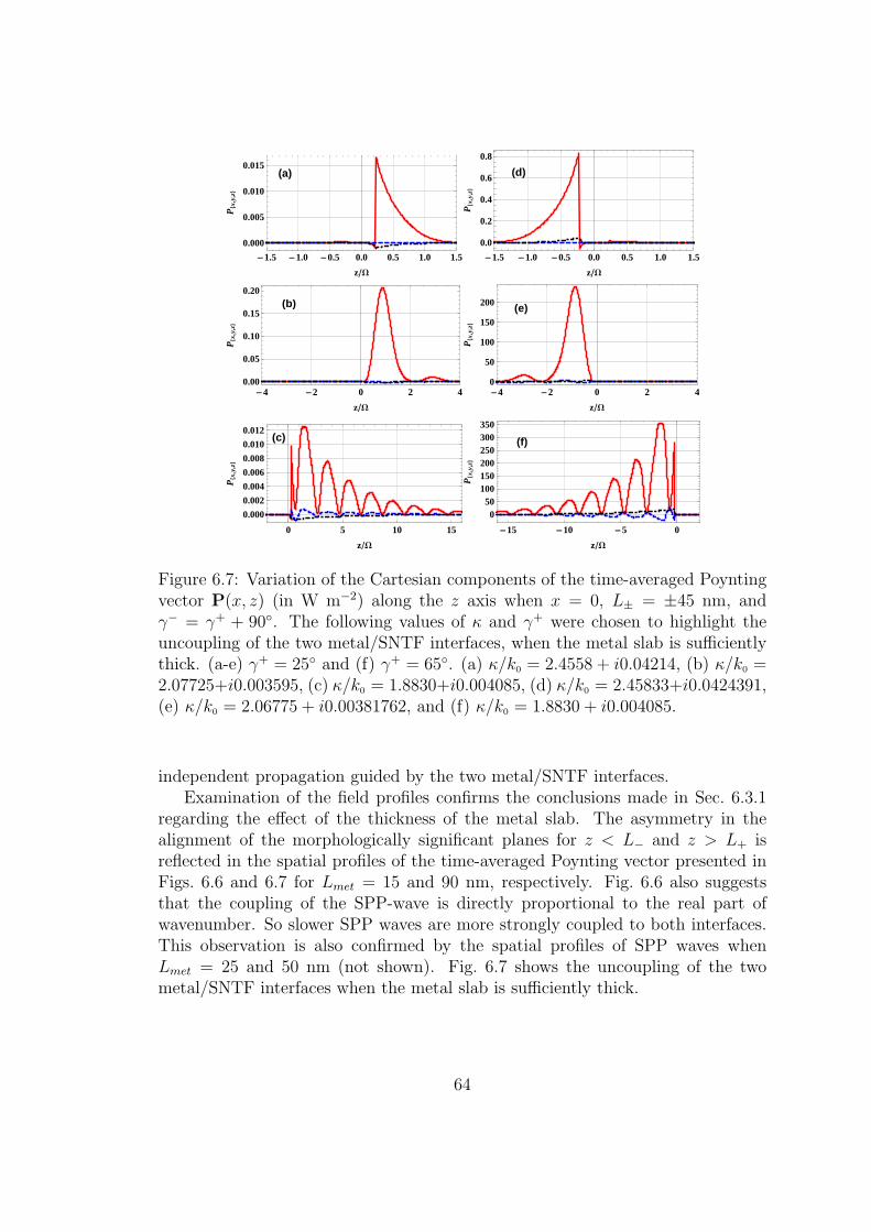
(a)
-1.5 -1.0 -0.5 0.0 0.5 1.0 1.5
0.000
0.005
0.010
0.015
zW
P8x
,y,z<
(d)
-1.5 -1.0 -0.5 0.0 0.5 1.0 1.5
0.0
0.2
0.4
0.6
0.8
zW
P8x
,y,z<
(b)
-4 -2 0 2 40.00
0.05
0.10
0.15
0.20
zW
P8x
,y,z<
(e)
-4 -2 0 2 40
50
100
150
200
zW
P8x
,y,z<
(c)
0 5 10 15
0.000
0.002
0.004
0.006
0.008
0.010
0.012
zW
P8x
,y,z<
(f)
-15 -10 -5 0
050
100150200250300350
zW
P8x
,y,z<
Figure 6.7: Variation of the Cartesian components of the time-averaged Poyntingvector P(x, z) (in W m−2) along the z axis when x = 0, L± = ±45 nm, andγ− = γ+ + 90. The following values of κ and γ+ were chosen to highlight theuncoupling of the two metal/SNTF interfaces, when the metal slab is sufficientlythick. (a-e) γ+ = 25 and (f) γ+ = 65. (a) κ/k0 = 2.4558 + i0.04214, (b) κ/k0 =2.07725+i0.003595, (c) κ/k0 = 1.8830+i0.004085, (d) κ/k0 = 2.45833+i0.0424391,(e) κ/k0 = 2.06775 + i0.00381762, and (f) κ/k0 = 1.8830 + i0.004085.
independent propagation guided by the two metal/SNTF interfaces.Examination of the field profiles confirms the conclusions made in Sec. 6.3.1
regarding the effect of the thickness of the metal slab. The asymmetry in thealignment of the morphologically significant planes for z < L− and z > L+ isreflected in the spatial profiles of the time-averaged Poynting vector presented inFigs. 6.6 and 6.7 for Lmet = 15 and 90 nm, respectively. Fig. 6.6 also suggeststhat the coupling of the SPP-wave is directly proportional to the real part ofwavenumber. So slower SPP waves are more strongly coupled to both interfaces.This observation is also confirmed by the spatial profiles of SPP waves whenLmet = 25 and 50 nm (not shown). Fig. 6.7 shows the uncoupling of the twometal/SNTF interfaces when the metal slab is sufficiently thick.
64
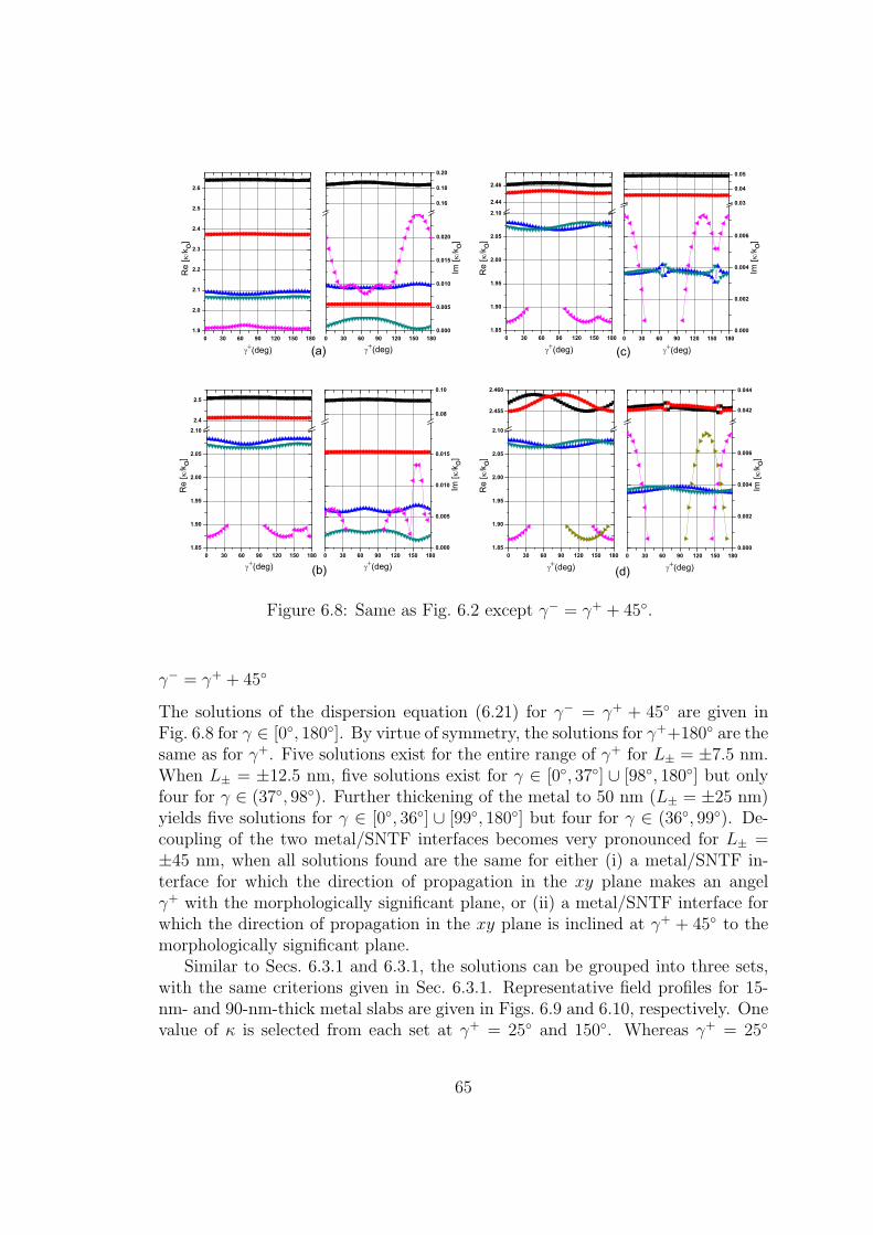
0 30 60 90 120 150 1801.9
2.0
2.1
2.2
2.3
2.4
2.5
2.6
0 30 60 90 120 150 1800.000
0.005
0.010
0.015
0.020
0.16
0.18
0.20
Re
[k o
]
(deg)
Im [
k o]
(deg)(a)0 30 60 90 120 150 180
1.85
1.90
1.95
2.00
2.05
2.10
2.44
2.46
0 30 60 90 120 150 1800.000
0.002
0.004
0.006
0.03
0.04
0.05
Re
[k o
]
(deg) (c)
Im [
k o]
(deg)
0 30 60 90 120 150 1801.85
1.90
1.95
2.00
2.05
2.10
2.4
2.5
0 30 60 90 120 150 1800.000
0.005
0.010
0.015
0.08
0.10
Re
[k o
]
(deg)
Im [
k o]
(deg)(b)0 30 60 90 120 150 180
1.85
1.90
1.95
2.00
2.05
2.10
2.455
2.460
0 30 60 90 120 150 1800.000
0.002
0.004
0.006
0.042
0.044
Re
[k o
]
(deg)
Im [
k o]
(deg)(d)
Figure 6.8: Same as Fig. 6.2 except γ− = γ+ + 45.
γ− = γ+ + 45
The solutions of the dispersion equation (6.21) for γ− = γ+ + 45 are given inFig. 6.8 for γ ∈ [0, 180]. By virtue of symmetry, the solutions for γ++180 are thesame as for γ+. Five solutions exist for the entire range of γ+ for L± = ±7.5 nm.When L± = ±12.5 nm, five solutions exist for γ ∈ [0, 37] ∪ [98, 180] but onlyfour for γ ∈ (37, 98). Further thickening of the metal to 50 nm (L± = ±25 nm)yields five solutions for γ ∈ [0, 36] ∪ [99, 180] but four for γ ∈ (36, 99). De-coupling of the two metal/SNTF interfaces becomes very pronounced for L± =±45 nm, when all solutions found are the same for either (i) a metal/SNTF in-terface for which the direction of propagation in the xy plane makes an angelγ+ with the morphologically significant plane, or (ii) a metal/SNTF interface forwhich the direction of propagation in the xy plane is inclined at γ+ + 45 to themorphologically significant plane.
Similar to Secs. 6.3.1 and 6.3.1, the solutions can be grouped into three sets,with the same criterions given in Sec. 6.3.1. Representative field profiles for 15-nm- and 90-nm-thick metal slabs are given in Figs. 6.9 and 6.10, respectively. Onevalue of κ is selected from each set at γ+ = 25 and 150. Whereas γ+ = 25
65
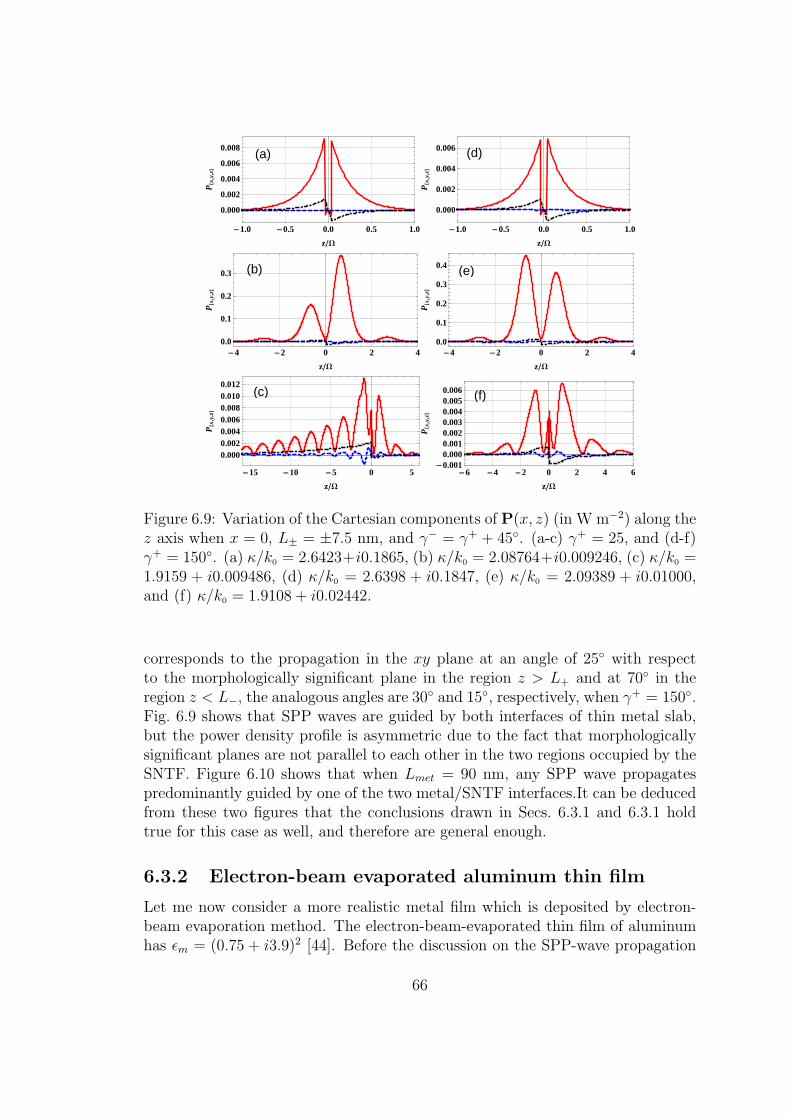
(a)
-1.0 -0.5 0.0 0.5 1.0
0.000
0.002
0.004
0.006
0.008
zW
P8x
,y,z<
(d)
-1.0 -0.5 0.0 0.5 1.0
0.000
0.002
0.004
0.006
zW
P8x
,y,z<
(b)
-4 -2 0 2 40.0
0.1
0.2
0.3
zW
P8x
,y,z<
(e)
-4 -2 0 2 40.0
0.1
0.2
0.3
0.4
zW
P8x
,y,z<
(c)
-15 -10 -5 0 5
0.0000.0020.0040.0060.0080.0100.012
zW
P8x
,y,z<
(f)
-6 -4 -2 0 2 4 6-0.001
0.0000.0010.0020.0030.0040.0050.006
zW
P8x
,y,z<
Figure 6.9: Variation of the Cartesian components of P(x, z) (in W m−2) along thez axis when x = 0, L± = ±7.5 nm, and γ− = γ+ + 45. (a-c) γ+ = 25, and (d-f)γ+ = 150. (a) κ/k0 = 2.6423+i0.1865, (b) κ/k0 = 2.08764+i0.009246, (c) κ/k0 =1.9159 + i0.009486, (d) κ/k0 = 2.6398 + i0.1847, (e) κ/k0 = 2.09389 + i0.01000,and (f) κ/k0 = 1.9108 + i0.02442.
corresponds to the propagation in the xy plane at an angle of 25 with respectto the morphologically significant plane in the region z > L+ and at 70 in theregion z < L−, the analogous angles are 30
and 15, respectively, when γ+ = 150.Fig. 6.9 shows that SPP waves are guided by both interfaces of thin metal slab,but the power density profile is asymmetric due to the fact that morphologicallysignificant planes are not parallel to each other in the two regions occupied by theSNTF. Figure 6.10 shows that when Lmet = 90 nm, any SPP wave propagatespredominantly guided by one of the two metal/SNTF interfaces.It can be deducedfrom these two figures that the conclusions drawn in Secs. 6.3.1 and 6.3.1 holdtrue for this case as well, and therefore are general enough.
6.3.2 Electron-beam evaporated aluminum thin film
Let me now consider a more realistic metal film which is deposited by electron-beam evaporation method. The electron-beam-evaporated thin film of aluminumhas ϵm = (0.75 + i3.9)2 [44]. Before the discussion on the SPP-wave propagation
66

(a)
-1.5 -1.0 -0.5 0.0 0.5 1.0 1.5
0.00.20.40.60.81.01.2
zW
P8x
,y,z<
(d)
-1.5 -1.0 -0.5 0.0 0.5 1.0 1.5
0.000
0.002
0.004
0.006
0.008
0.010
zW
P8x
,y,z<
(b)
-4 -2 0 2 40.00
0.05
0.10
0.15
0.20
zW
P8x
,y,z<
(e)
-4 -3 -2 -1 0 10
50
100
150
zW
P8x
,y,z<
(c)
-2 0 2 4 6 8 10 12
0.000
0.002
0.004
0.006
0.008
0.010
zW
P8x
,y,z<
(f)
-12 -10 -8 -6 -4 -2 0 2
0
2
4
6
8
10
zW
P8x
,y,z<
Figure 6.10: Same as Fig. 6.9 except that L± = ±45 nm. (a) κ/k0 = 2.4586 +i0.04246, (b) κ/k0 = 2.07725 + i0.003595, (c) κ/k0 = 1.8891 + i0.002576, (d)κ/k0 = 2.4559+ i0.04227, (e) κ/k0 = 2.07916+ i0.003560, and (f) κ/k0 = 1.8737+i0.006143.
0 15 30 45 60 75 90
1.5
1.8
2.1
2.4
2.7
0 15 30 45 60 75 900.000
0.005
0.010
0.015
0.020
0.20
0.25
Re
[k o
]
(deg)
Im [
k o]
(deg)
Figure 6.11: Real and imaginary parts of κ/k0, which represent SPP-wave prop-agation guided by the single interface of the chosen SNTF and electron-beam-evaporated aluminum: ϵm = (0.75 + i3.9)2.
67
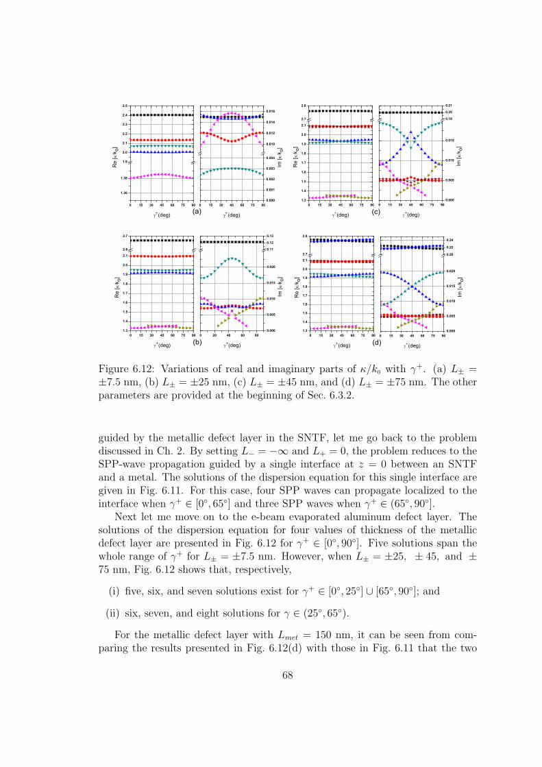
0 15 30 45 60 75 90
1.36
1.38
1.9
2.0
2.1
2.2
2.3
2.4
2.5
0 15 30 45 60 75 900.000
0.001
0.002
0.003
0.004
0.010
0.012
0.014
0.016
(a)
Re
[k o
]
(deg)
Im [
k o]
(deg)
0 15 30 45 60 75 901.3
1.4
1.5
1.6
1.7
1.8
1.9
2.0
2.1
2.7
2.8
0 15 30 45 60 75 900.000
0.005
0.010
0.015
0.19
0.20
0.21
(c)
Re
[k o
]
(deg)
Im [
k o]
(deg)
0 15 30 45 60 75 901.3
1.4
1.5
1.6
1.7
1.8
1.9
2.0
2.1
2.6
2.7
0 20 40 60 800.000
0.005
0.010
0.015
0.020
0.11
0.12
0.13
(b)
Re
[k o
]
(deg)
Im [
k o]
(deg)
0 15 30 45 60 75 901.3
1.4
1.5
1.6
1.7
1.8
1.9
2.0
2.1
2.7
2.8
0 15 30 45 60 75 900.000
0.005
0.010
0.015
0.020
0.20
0.22
0.24
(d)
Re
[k o
]
(deg)
Im [
k o]
(deg)
Figure 6.12: Variations of real and imaginary parts of κ/k0 with γ+. (a) L± =±7.5 nm, (b) L± = ±25 nm, (c) L± = ±45 nm, and (d) L± = ±75 nm. The otherparameters are provided at the beginning of Sec. 6.3.2.
guided by the metallic defect layer in the SNTF, let me go back to the problemdiscussed in Ch. 2. By setting L− = −∞ and L+ = 0, the problem reduces to theSPP-wave propagation guided by a single interface at z = 0 between an SNTFand a metal. The solutions of the dispersion equation for this single interface aregiven in Fig. 6.11. For this case, four SPP waves can propagate localized to theinterface when γ+ ∈ [0, 65] and three SPP waves when γ+ ∈ (65, 90].
Next let me move on to the e-beam evaporated aluminum defect layer. Thesolutions of the dispersion equation for four values of thickness of the metallicdefect layer are presented in Fig. 6.12 for γ+ ∈ [0, 90]. Five solutions span thewhole range of γ+ for L± = ±7.5 nm. However, when L± = ±25, ± 45, and ±75 nm, Fig. 6.12 shows that, respectively,
(i) five, six, and seven solutions exist for γ+ ∈ [0, 25] ∪ [65, 90]; and
(ii) six, seven, and eight solutions for γ ∈ (25, 65).
For the metallic defect layer with Lmet = 150 nm, it can be seen from com-paring the results presented in Fig. 6.12(d) with those in Fig. 6.11 that the two
68

(a)
-2 -1 0 1 2-0.02
0.00
0.02
0.04
0.06
zW
P8x
,y,z< (d)
-2 -1 0 1 2-0.005
0.0000.0050.0100.015
zW
P8x
,y,z<
(b)
-4 -2 0 2 40.000.020.040.060.080.10
zW
P8x
,y,z<
(e)
-4 -2 0 2 40.0000.0050.0100.0150.0200.0250.030
zW
P8x
,y,z<
(c)
-10 -5 0 5 100.0
0.5
1.0
1.5
zW
P8x
,y,z<
(f)
-10 -5 0 5 10
0.00.51.01.52.02.5
zW
P8x
,y,z<
Figure 6.13: Variation of the Cartesian components of the time-averaged Poyntingvector P(x, z) (in W m−2) along the z axis when x = 0, L± = ±7.5 nm. (a-c) γ+ = 0, and (d-f) γ+ = 25. The following values of κ were to highlightthe coupled SPP-waves propagation: (a) κ/k0 = 2.40502 + i0.015, (b) κ/k0 =2.06954 + i0.00239, (c) κ/k0 = 1.38082 + i0.00969, (d) κ/k0 = 2.40519 + i0.01502,(e) κ/k0 = 2.07249+i0.00297, and (f) κ/k0 = 1.38392+i0.01444. The componentsparallel to ux, uy, and uz, are represented by red solid, blue dashed, and blackchain-dashed lines, respectively.
metal/SNTF interfaces are actually uncoupled from each other. The solutionsin Fig. 6.12(d) represent SPP-wave propagation guided independently by the twometal/SNTF interfaces (as in Fig. 6.11). It can be concluded that, as the thicknessof the metallic defect layer is increased, the coupling between two metal/SNTFinterfaces located at z = L− and z = L+ decreases; ultimately, the two interfacesdecouple from each other when the thickness Lmet significantly exceeds twice the
skin depth ∆met =[Im(k0
√ϵm)]−1
in the metal. The skin depth in the electron-beam-evaporated aluminum thin film at the chosen wavelength is 24.91 nm.
The solutions in Fig. 6.12 can be divided into four sets. The first set comprisesthose solutions for which Re(κ/k0) lies between 2.3 and 2.8. This set has only onebranch representing the coupled SPP-wave propagation when Lmet = 15 nm, but it
69
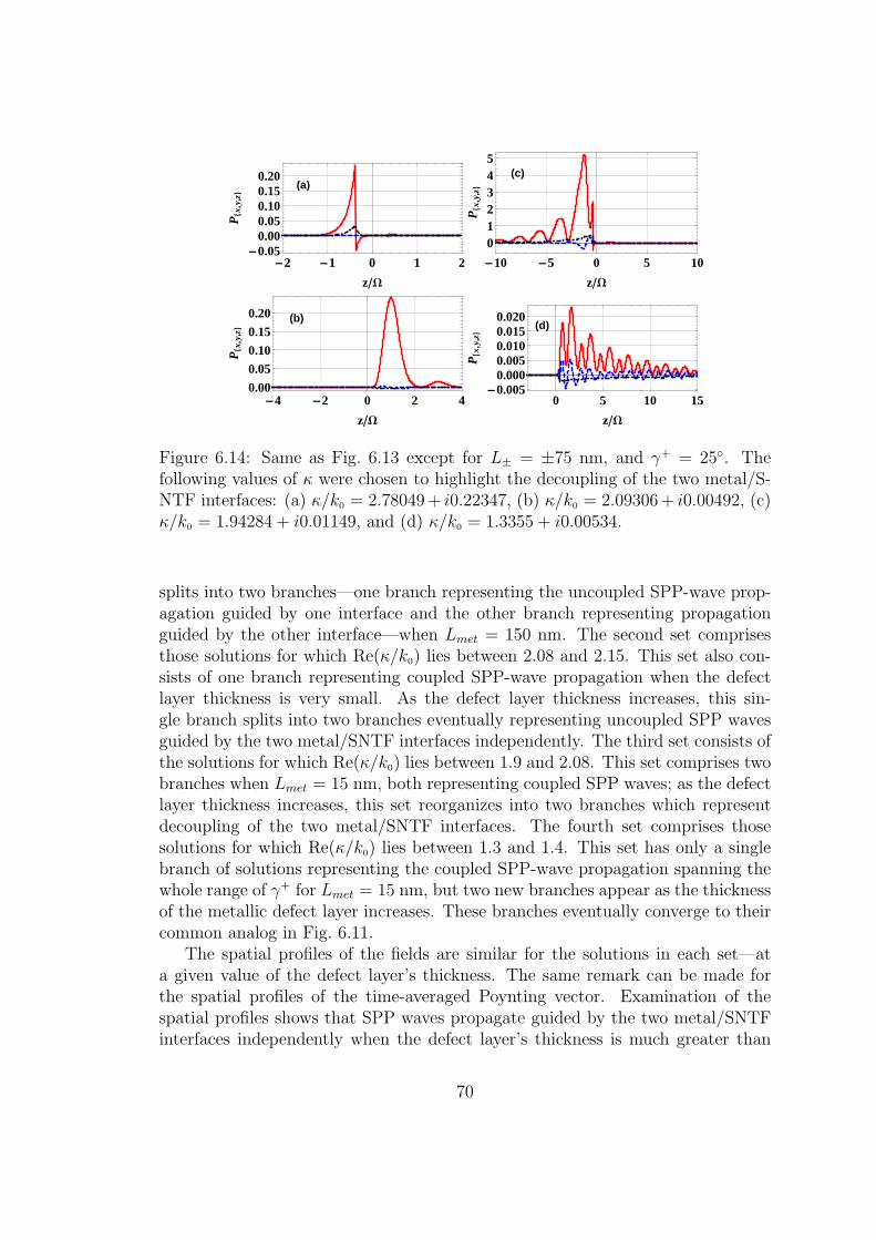
(a)
-2 -1 0 1 2-0.05
0.000.050.100.150.20
zW
P8x
,y,z<
(c)
-10 -5 0 5 10
012345
zW
P8x
,y,z<
(b)
-4 -2 0 2 40.00
0.05
0.10
0.15
0.20
zW
P8x
,y,z< (d)
0 5 10 15-0.005
0.0000.0050.0100.0150.020
zW
P8x
,y,z<
Figure 6.14: Same as Fig. 6.13 except for L± = ±75 nm, and γ+ = 25. Thefollowing values of κ were chosen to highlight the decoupling of the two metal/S-NTF interfaces: (a) κ/k0 = 2.78049+ i0.22347, (b) κ/k0 = 2.09306+ i0.00492, (c)κ/k0 = 1.94284 + i0.01149, and (d) κ/k0 = 1.3355 + i0.00534.
splits into two branches—one branch representing the uncoupled SPP-wave prop-agation guided by one interface and the other branch representing propagationguided by the other interface—when Lmet = 150 nm. The second set comprisesthose solutions for which Re(κ/k0) lies between 2.08 and 2.15. This set also con-sists of one branch representing coupled SPP-wave propagation when the defectlayer thickness is very small. As the defect layer thickness increases, this sin-gle branch splits into two branches eventually representing uncoupled SPP wavesguided by the two metal/SNTF interfaces independently. The third set consists ofthe solutions for which Re(κ/k0) lies between 1.9 and 2.08. This set comprises twobranches when Lmet = 15 nm, both representing coupled SPP waves; as the defectlayer thickness increases, this set reorganizes into two branches which representdecoupling of the two metal/SNTF interfaces. The fourth set comprises thosesolutions for which Re(κ/k0) lies between 1.3 and 1.4. This set has only a singlebranch of solutions representing the coupled SPP-wave propagation spanning thewhole range of γ+ for Lmet = 15 nm, but two new branches appear as the thicknessof the metallic defect layer increases. These branches eventually converge to theircommon analog in Fig. 6.11.
The spatial profiles of the fields are similar for the solutions in each set—ata given value of the defect layer’s thickness. The same remark can be made forthe spatial profiles of the time-averaged Poynting vector. Examination of thespatial profiles shows that SPP waves propagate guided by the two metal/SNTFinterfaces independently when the defect layer’s thickness is much greater than
70
twice the penetration depth in the metal. As that thickness is reduced, couplingof the two interfaces results in new SPP waves. The smaller is the thickness of themetallic defect layer, the stronger is the coupling effect.
The asymmetry in the alignment of the morphologically significant planes forz < L− and z > L+ is reflected in the spatial profiles of the time-averaged Poyntingvector presented in Figs. 6.13 and 6.14 for Lmet = 15 and 150 nm, respectively.In Fig. 6.13, the variations of the Cartesian components of P for γ+ = 0 and25 and for three values of κ—selected from the first, third and fourth sets—aregiven to show the coupled SPP-wave propagation. Figure 6.13 also suggests thatthe coupling is directly proportional to the real part of the wavenumber κ. Hence,slower SPP waves are more strongly coupled to both interfaces. This observationis also confirmed by the spatial profiles of SPP waves when Lmet = 50 and 90 nm(not shown). To highlight the uncoupled SPP-wave propagation guided by the twointerfaces independently when Lmet = 150 nm, the spatial distribution of powerdensity is shown in Fig. 6.14. For these plots one solution was selected from eachset at γ+ = 25.
6.4 Concluding Remarks
The canonical boundary-value problem to examine the characteristics of SPPwaves guided by a thin metal slab inserted in a periodically nonhomogeneousSNTF is formulated and numerically solved. The morphologically significantplanes on the two sides of the metal slab could be either parallel to or twistedwith respect to each other. It was found that
(i) when the metal slab is very thin, its two interfaces with the SNTF coupleto each other, thereby generating more modes of SPP-wave propagation;
(ii) as the metal slab thickness increases, the coupling between the two interfacesdecreases;
(iii) both the phase speed and the attenuation of an SPP wave depend on thetwist between the morphologically significant planes of the SNTF on the twosides of the metal slab;
(iv) smaller phase speeds are obtained with a thinner metal slab; and
(v) the two interfaces of a sufficiently thick metal slab with the SNTF indepen-dently guide SPP waves.
The results for bulk aluminum and an electron-beam evaporated thin film aresimilar except for the different penetration depths.
71
Chapter 7
Guided-Wave Propagation by aDielectric Slab in an SNTF‡
7.1 Introduction
The last two decades have opened new technoscientific avenues, including the ca-pability to design materials with nanoscale morphology [97–99]. Since solid-statetechnology is mostly planar, the need for two distinct modalities of guided-wavepropagation, among others, has arisen. First, efficient planar optical waveguidesin the cladding/core/cladding configuration are needed to transport optical sig-nals [100]; second, surface-plasmon-polariton (SPP) waves guided by planar met-al/dielectric interfaces are attractive as they are faster than purely electronic wavestraveling in good conductors [13, 14]. A major challenge to the adoption of SPP-based communication is the high attenuation of SPP waves [101], as becomesevident from the solutions of a relevant canonical boundary-value problem [102],primarily due to ohmic losses in the metal. Though several mitigation strategiesare being tried out [41], an obvious one is to replace the metal by a dielectricmaterial. That is the attraction of Dyakonov–Tamm waves.
Because of continued interest in conventional dielectric waveguides and opti-cal surface waves, I decided to find a structure which can transport electromag-netic energy via waveguide modes and Dyakonov–Tamm waves. The interface ofa homogeneous, isotropic dielectric material and a periodically nonhomogeneousSNTF [70] can support Dyakonov–Tamm waves [64]. Therefore, I set out to inves-tigate wave propagation guided by a homogeneous, isotropic dielectric slab insertedin a periodically nonhomogeneous SNTF, the dielectric slab being the core andthe SNTF being the cladding. The structure thus formed can be considered to bea canonical structure that allows (i) interaction between waves localized to differ-
‡This chapter is based on: M. Faryad and A. Lakhtakia, “Propagation of surface waves andwaveguide modes guided by a dielectric slab inserted in a sculptured nematic thin film,” Phys.Rev. A. 83, 013814 (2011).
72
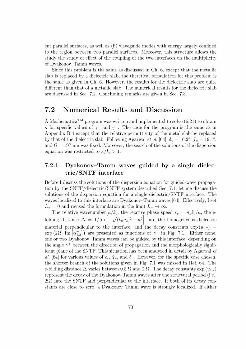
ent parallel surfaces, as well as (ii) waveguide modes with energy largely confinedto the region between two parallel surfaces. Moreover, this structure allows thestudy the study of effect of the coupling of the two interfaces on the multiplicityof Dyakonov–Tamm waves.
Since this problem is the same as discussed in Ch. 6, except that the metallicslab is replaced by a dielectric slab, the theretical formulation for this problem isthe same as given in Ch. 6. However, the results for the dielectric slab are quitedifferent than that of a metallic slab. The numerical results for the dielectric slabare discussed in Sec. 7.2. Concluding remarks are given in Sec. 7.3.
7.2 Numerical Results and Discussion
A MathematicaTM program was written and implemented to solve (6.21) to obtainκ for specific values of γ+ and γ−. The code for the program is the same as inAppendix B.4 except that the relative permittivity of the metal slab be replacedby that of the dielectric slab. Following Agarwal et al. [64], δv = 16.2, χv = 19.1,and Ω = 197 nm was fixed. Moreover, the search of the solutions of the dispersionequation was restricted to κ/k0 > 1.
7.2.1 Dyakonov–Tamm waves guided by a single dielec-tric/SNTF interface
Before I discuss the solutions of the dispersion equation for guided-wave propaga-tion by the SNTF/dielectric/SNTF system described Sec. 7.1, let me discuss thesolutions of the dispersion equation for a single dielectric/SNTF interface. Thewaves localized to this interface are Dyakonov–Tamm waves [64]. Effectively, I setL+ = 0 and revised the formulation in the limit L− → ∞.
The relative wavenumber κ/k0, the relative phase speed vr = nsk0/κ, the e-
folding distance ∆ = 1/Im[+√
(k0ns)2 − κ2]into the homogeneous dielectric
material perpendicular to the interface, and the decay constants exp (u1,2) =exp
(2Ω · Im
[α+1,2
])are presented as functions of γ+ in Fig. 7.1. Either none,
one or two Dyakonov–Tamm waves can be guided by this interface, depending onthe angle γ+ between the direction of propagation and the morphologically signif-icant plane of the SNTF. This situation has been analyzed in detail by Agarwal etal. [64] for various values of ϵs, χv, and δv. However, for the specific case chosen,the shorter branch of the solutions given in Fig. 7.1 was missed in Ref. 64. Thee-folding distance ∆ varies between 0.8 Ω and 2 Ω. The decay constants exp (u1,2)represent the decay of the Dyakonov–Tamm waves after one structural period (i.e.,2Ω) into the SNTF and perpendicular to the interface. If both of its decay con-stants are close to zero, a Dyakonov–Tamm wave is strongly localized. If either
73
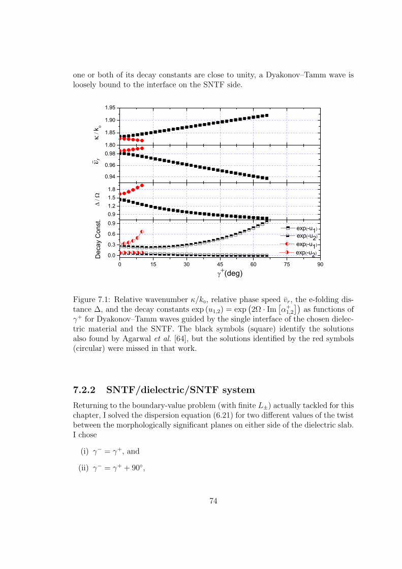
one or both of its decay constants are close to unity, a Dyakonov–Tamm wave isloosely bound to the interface on the SNTF side.
1.80
1.85
1.90
1.95
0.94
0.96
0.98
0.91.21.51.8
0 15 30 45 60 75 90
0.0
0.3
0.6
0.9
k o
exp(-u2)
exp(-u1)
exp(-u2)
exp(-u1)
Dec
ay C
onst
.
(deg)
Figure 7.1: Relative wavenumber κ/k0, relative phase speed vr, the e-folding dis-tance ∆, and the decay constants exp (u1,2) = exp
(2Ω · Im
[α+1,2
])as functions of
γ+ for Dyakonov–Tamm waves guided by the single interface of the chosen dielec-tric material and the SNTF. The black symbols (square) identify the solutionsalso found by Agarwal et al. [64], but the solutions identified by the red symbols(circular) were missed in that work.
7.2.2 SNTF/dielectric/SNTF system
Returning to the boundary-value problem (with finite L±) actually tackled for thischapter, I solved the dispersion equation (6.21) for two different values of the twistbetween the morphologically significant planes on either side of the dielectric slab.I chose
(i) γ− = γ+, and
(ii) γ− = γ+ + 90,
74
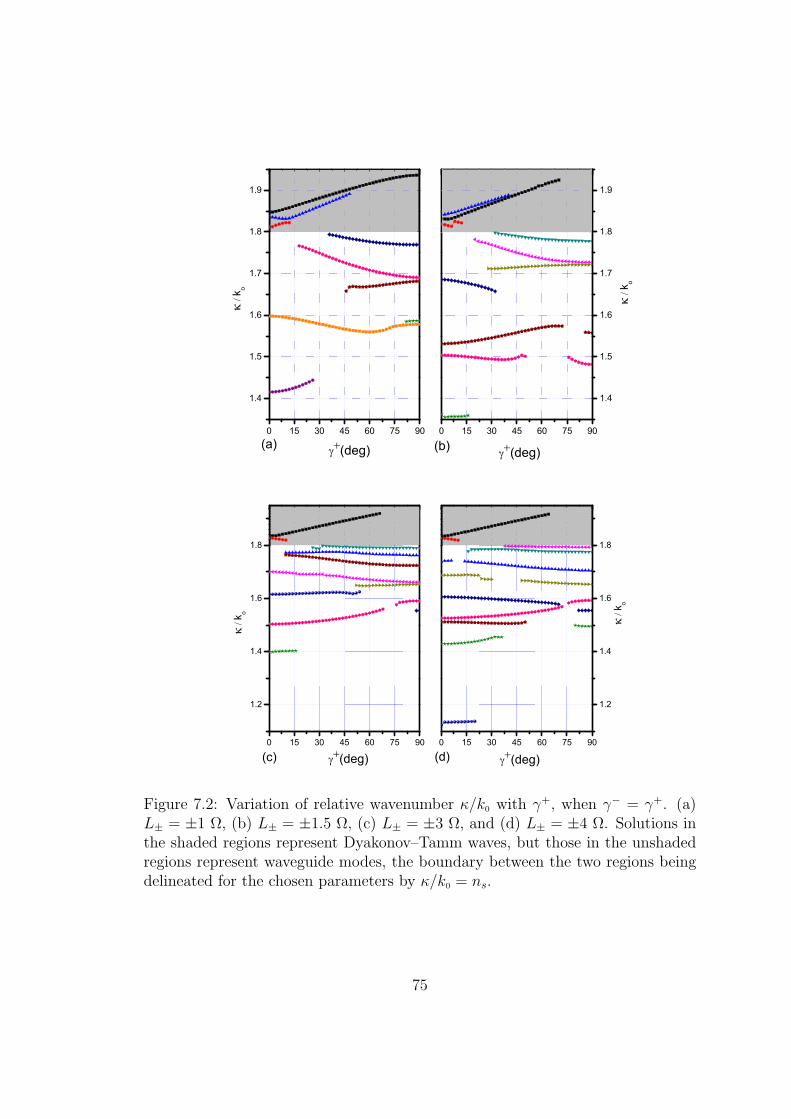
0 15 30 45 60 75 90
1.4
1.5
1.6
1.7
1.8
1.9
0 15 30 45 60 75 90
1.4
1.5
1.6
1.7
1.8
1.9
k o
k o
(deg)
(deg)(b)(a)
0 15 30 45 60 75 90
1.2
1.4
1.6
1.8
0 15 30 45 60 75 90
1.2
1.4
1.6
1.8
(d)(deg)
k o
k o
(c) (deg)
Figure 7.2: Variation of relative wavenumber κ/k0 with γ+, when γ− = γ+. (a)L± = ±1 Ω, (b) L± = ±1.5 Ω, (c) L± = ±3 Ω, and (d) L± = ±4 Ω. Solutions inthe shaded regions represent Dyakonov–Tamm waves, but those in the unshadedregions represent waveguide modes, the boundary between the two regions beingdelineated for the chosen parameters by κ/k0 = ns.
75

while γ+ was kept as a variable. For each choice, the boundaries of the dielectricslab were taken to be L± = ±Ω, ±1.5 Ω, ±3 Ω, or ±4 Ω nm. These selectionswere made so as to have Ls to be less than and greater than twice the e-foldingdistance ∆ within the dielectric slab along the z axis, in order to study the effectof coupling of the two interfaces.
γ− = γ+
Let me begin with the case when the morphologically significant planes of theSNTF on both sides of the dielectric slab are aligned with each other and make anangle γ− = γ+ with respect to the direction of wave propagation in the xy plane.By virtue of symmetry, the solutions for 180 + γ+ and 360 − γ+ are the same asfor γ+.
The solutions of the dispersion equation for various values of slab thickness—given in Fig. 7.2 as functions of γ+ ∈ [0, 90]—can be grouped into two categories,based on the value of κ. Within the dielectric slab, kz = +
√(k0ns)2 − κ2 is the
wavenumber along the z axis. If κ/k0 > ns, kz/k0 must be a complex number,signifying that these solutions do not represent waveguide modes, but Dyakonov–Tamm waves localized to the interfaces between the dielectric slab and the SNTF.However, the solution of the dispersion equation with κ/k0 < ns represent waveg-uide modes as kz would be a real number. This categorization is supported by acomparative analysis of the solutions presented in Figs. 7.1 and 7.2 as follows.
The solutions given in Fig. 7.2(a) for L± = ±Ω may be organized in threebranches with κ/k0 > ns and several branches with κ/k0 < ns. As the slabthickness Ls increases to 8 Ω in Fig. 7.2(d), the three branches with κ/k0 > ns
merge into two branches, but the number of branches for κ/k0 < ns goes onincreasing. The decrease in the number of solutions representing Dyakonov–Tammwaves is due to the uncoupling of the two interfaces z = L− and z = L+ as thethickness L+ − L− increases.
For L± = ±Ω, the slab thickness Ls is smaller than twice the e-folding distance∆ = 1/Im (kz). Hence, due to the coupling of the two interfaces I have moresolutions representing Dyakonov–Tamm waves. But Ls > 2∆ when L± = ±4 Ω(because ∆/Ω ∈ [0.8, 2]), and the two dielectric/SNTF interfaces are uncoupledfrom each other so that I have exactly the same solutions with κ/k0 > ns, as givenin Fig. 7.1 for a single dielectric/SNTF interface.
The increase in the number of waveguide modes with the increase in the thick-ness Ls of the dielectric slab is in accordance with the general behavior of waveg-uiding structures [104, 105]: the number of waveguide modes increases with theincrease in the cross-sectional dimensions of a waveguide.
The foregoing analysis is buttressed by the spatial profiles of the time-averagedPoynting vector
P(x, z) =1
2Re [E(x, z)×H∗(x, z)] ; (7.1)
76

(a)
-4 -2 0 2 40.0000.0010.0020.0030.0040.0050.0060.007
zW
P8x
,y,z<
(b)
-6 -4 -2 0 2 4 6
0.000
0.001
0.002
0.003
0.004
zW
P8x
,y,z<
(c)
-6 -4 -2 0 2 4 6
0.0000.0020.0040.0060.0080.010
zW
P8x
,y,z<
(d)
-4 -2 0 2 40.0
0.2
0.4
0.6
0.8
1.0
zW
P8x
,y,z<
(e)
-4 -2 0 2 40.00
0.05
0.10
0.15
zW
P8x
,y,z<
(f)
-6 -4 -2 0 2 4 6
0.0000.0050.0100.0150.0200.025
zW
P8x
,y,z<
Figure 7.3: Variation of the Cartesian components of P(z) (in W m−2) with z forγ− = γ+ and L± = ±Ω. The x-, y-, and z-directed components are representedby solid red, dashed blue and chain-dashed black lines. The orange-shaded regionrepresents the dielectric slab. γ+ = (a-d) 10 and (e-f) 80. κ/k0 = (a) 1.85608,(b) 1.83154, (c) 1.82269, (d) 1.59488, (e) 1.77007, and (f) 1.69357.
as κ is real, P(x, z) ≡ P(z). Representative plots of P(z) against z are presentedin Figs. 7.3 and 7.4 for four values of κ at γ+ = 10 and two values of κ atγ+ = 80. These spatial profiles were calculated by setting A+
1 = 1 Vm−1 anddetermining the remaining coefficients using Eq. (6.20). The shaded region in eachplot represents the region occupied by the dielectric slab. Each of Figs. 7.3(a), (b),and (c) represents the spatial profile of the power density of a Dyakonov–Tammwave, as the relative wavenumber κ/k0 > ns and the power density is strong ator close to the interfaces. In contrast, Figs. 7.3(d), (e), and (f) contain waveguidemodes because κ/k0 < ns.
The distinction between Dyakonov–Tamm waves and the waveguide modes ismore evident in the spatial profiles presented in Fig. 7.4 for L± = ±4 Ω. Thespatial profiles given in Figs. 7.4(a) and (b) represent Dyakonov–Tamm waves,whereas Figs. 7.4(c), (d), (e), and (f) contain the spatial profiles of waveguidemodes. Some of the waveguide modes do have maximums in their profiles at ornear the two dielectric SNTF/interfaces, but some other waveguide modes containmost of the power near the central axis.
77
(a)
-10 -5 0 5 100.0000.0010.0020.0030.0040.0050.006
zW
P8x
,y,z<
(b)
-15 -10 -5 0 5 10 150.000
0.002
0.004
0.006
zW
P8x
,y,z<
(c)
-10 -5 0 5 100.0
0.5
1.0
1.5
zW
P8x
,y,z<
(d)
-10 -5 0 5 100.00
0.05
0.10
0.15
zW
P8x
,y,z<
(e)
-10 -5 0 5 100.0
0.2
0.4
0.6
0.8
zW
P8x
,y,z<
(f)
-10 -5 0 5 10
0.000
0.005
0.010
0.015
0.020
zW
P8x
,y,z<
Figure 7.4: Same as Fig. 7.3 except for L± = ±4Ω and κ/k0 = (a) 1.84489, (b)1.81941, (c) 1.60496, (d) 1.5111, (e) 1.79381, and (f) 1.70705.
γ− = γ+ + 90
The solutions of the dispersion equation for γ− = γ+ + 90—the morphologicallysignificant planes of the SNTF on both sides are perpendicular to each other—aregiven in Fig. 7.5 as functions of γ+ ∈ [0, 90] for various values of slab thickness.Due to the symmetry of the problem, the solutions for 90±γ+, 180±γ+, 270±γ+and 360 − γ+ are the same as for γ+.
The solutions for this case can also be divided into two categories based on thevalue of κ/k0. The solutions with κ/k0 > ns represent Dyakonov–Tamm wavesthat strongly couple to either one or both of the dielectric/SNTF interfaces, whilethe solutions with κ/k0 < ns represent waveguide modes. For the thinnest dielec-tric slab, there are three branches representing Dyakonov–Tamm waves that arecoupled to both interfaces. As the slab thickness increases up to 8 Ω, the couplingdiminishes and the solutions representing Dyakonov–Tamm waves eventually be-come identical to the solutions of two independent dielectric/SNTF interfaces withthe morphologically significant plane located either at γ+ = 0 or at γ+ = 90. TheDyakonov–Tamm waves propagate independently guided by individual interfacesfor Ls = 8 Ω because the slab thickness is then much greater than the e-foldingdistance ∆ for all γ+. The number of solution branches representing waveguidemodes increases as the thickness of the dielectric slab increases from 2 Ω to 8 Ω.
Representative plots of P(z) vs. z for L± = ±1 Ω are given in Fig. 7.6 for three
78
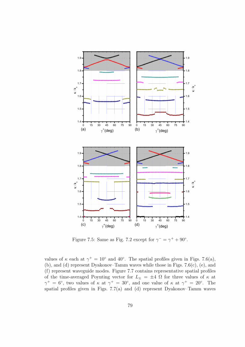
0 15 30 45 60 75 901.4
1.5
1.6
1.7
1.8
1.9
0 15 30 45 60 75 901.4
1.5
1.6
1.7
1.8
1.9
k o
(deg)
k o
(deg)(b)(a)
0 15 30 45 60 75 901.4
1.5
1.6
1.7
1.8
1.9
0 15 30 45 60 75 901.4
1.5
1.6
1.7
1.8
1.9
(deg)
k o
(deg)(d)(c)
k o
Figure 7.5: Same as Fig. 7.2 except for γ− = γ+ + 90.
values of κ each at γ+ = 10 and 40. The spatial profiles given in Figs. 7.6(a),(b), and (d) represent Dyakonov–Tamm waves while those in Figs. 7.6(c), (e), and(f) represent waveguide modes. Figure 7.7 contains representative spatial profilesof the time-averaged Poynting vector for L± = ±4 Ω for three values of κ atγ+ = 6, two values of κ at γ+ = 30, and one value of κ at γ+ = 20. Thespatial profiles given in Figs. 7.7(a) and (d) represent Dyakonov–Tamm waves
79
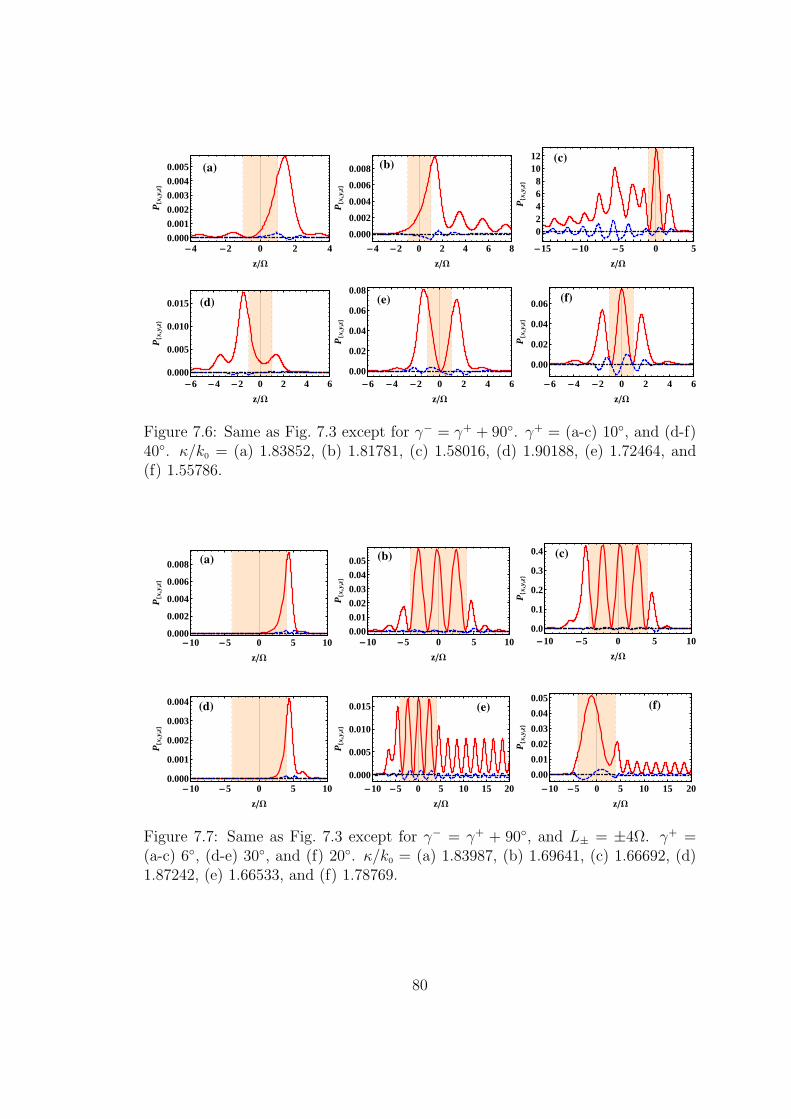
(a)
-4 -2 0 2 40.000
0.001
0.002
0.003
0.004
0.005
zW
P8x
,y,z<
(b)
-4 -2 0 2 4 6 8
0.000
0.002
0.004
0.006
0.008
zW
P8x
,y,z<
(c)
-15 -10 -5 0 5
02468
1012
zW
P8x
,y,z<
(d)
-6 -4 -2 0 2 4 60.000
0.005
0.010
0.015
zW
P8x
,y,z<
(e)
-6 -4 -2 0 2 4 60.00
0.02
0.04
0.06
0.08
zW
P8x
,y,z<
(f)
-6 -4 -2 0 2 4 6
0.00
0.02
0.04
0.06
zW
P8x
,y,z<
Figure 7.6: Same as Fig. 7.3 except for γ− = γ+ + 90. γ+ = (a-c) 10, and (d-f)40. κ/k0 = (a) 1.83852, (b) 1.81781, (c) 1.58016, (d) 1.90188, (e) 1.72464, and(f) 1.55786.
(a)
-10 -5 0 5 100.000
0.002
0.004
0.006
0.008
zW
P8x
,y,z<
(b)
-10 -5 0 5 100.00
0.01
0.02
0.03
0.04
0.05
zW
P8x
,y,z<
(c)
-10 -5 0 5 100.0
0.1
0.2
0.3
0.4
zW
P8x
,y,z<
(d)
-10 -5 0 5 100.000
0.001
0.002
0.003
0.004
zW
P8x
,y,z<
(e)
-10 -5 0 5 10 15 200.000
0.005
0.010
0.015
zW
P8x
,y,z<
(f)
-10 -5 0 5 10 15 20
0.00
0.01
0.02
0.03
0.04
0.05
zW
P8x
,y,z<
Figure 7.7: Same as Fig. 7.3 except for γ− = γ+ + 90, and L± = ±4Ω. γ+ =(a-c) 6, (d-e) 30, and (f) 20. κ/k0 = (a) 1.83987, (b) 1.69641, (c) 1.66692, (d)1.87242, (e) 1.66533, and (f) 1.78769.
80
localized to one interface while the profiles given in Figs. 7.7(b), (c), (e), and (f)represent waveguide modes. However, in Figs. 7.7(e) and (f) the decay rate of theDyakonov–Tamm wave in the SNTF z > L+ is very low. The asymmetry in thepower profiles in Figs. 7.6 and 7.7 is due to the asymmetry in the arrangement ofthe morphologically significant planes of the SNTF on either side of the dielectricslab.
Before continuing, let me note that Dyakonov–Tamm waves alone would prop-agate if the dielectric slab were to be absent (i.e. Ls = 0), as has been shown inCh. 5.
Analysis of Figs. 7.1, 7.2 and 7.5 reveals a major advantage of using the SNT-F/dielectric/SNTF system for the propagation of Dyakonov–Tamm waves as com-pared to the single SNTF/dielectric interface: the angular range of propagationand the possible number of Dyakonov–Tamm waves can be increased if the thick-ness of the dielectric slab is sufficiently small. Guided by a single SNTF/dielectricinterface, two Dyakonov–Tamm waves can propagate for γ+ ∈ [0, 10], one forγ+ ∈ (10, 66], and none for γ+ ∈ (66, 90]. However, the presented data indi-cate that an SNTF/dielectric/SNTF system with a dielectric slab of thickness 2Ωor less can support the propagation of
• three Dyakonov–Tamm waves for γ+ ∈ [0, 10], two for γ+ ∈ (10, 48], andone for γ+ ∈ (48, 90], when γ− = γ+,
• two Dyakonov–Tamm waves for γ+ ∈ [0, 10] ∪ [22, 68] ∪ [80, 90] andone for γ+ ∈ (10, 22) ∪ (68, 80), when γ− = γ+ + 90.
7.2.3 Comparison with SNTF/metal/SNTF system of Ch. 6
Wave propagation guided by an aluminum slab inserted in a periodically non-homogeneous SNTF was studied in detail in Ch. 6 for Ω = 200 nm, χv = 45
and δv = 30. However, similar calculations with Ω = 197 nm, χv = 19.1 andδv = 16.2 were performed, for direct comparison with the data presented in Figs.7.2–7.7, and the results showed same characteristics as in Ch. 6. The waves prop-agating in the SNTF/metal/SNTF system are classified as SPP waves which maybe coupled to either one or both of the metal/SNTF interfaces, depending on thethickness of metal slab.
Some attributes of wave propagation in the SNTF/metal/SNTF system aresimilar to those of guided-wave propagation in the SNTF/dielectric/SNTF system,but others are not. The following differences were noted:
• The wavenumber κ is a complex number for the SNTF/metal/SNTF systemP(x, z) = P(z) exp [−2Im(κ)x], but real for the SNTF/dielectric/SNTF sys-tem so that P(x, z) = P(z). Consequently, whereas attenuation must occurin the direction of propagation in the SNTF/metal/SNTF system, but thepropagation is lossless in the SNTF/dielectric/SNTF system.
81
• The dielectric core can support the propagation of waveguide modes whereasthe metallic core cannot. Therefore, both surface waves (Dyakonov–Tammwaves) and waveguide modes can propagate in the SNTF/dielectric/SNTFsystem, but only surface waves (SPP waves) can propagate in the SNT-F/metal/SNTF system.
• Coupling between the two interfaces exists only for very thin metal slabs(Ls . 60 nm), but for much thicker dielectric slabs (Ls . 1000 nm). This isbecause the imaginary parts of the relative permittivities of metals are veryhigh in the optical regime, but those of commonplace dielectric materials arevanishingly small.
• When both the morphologically significant planes of the SNTF on either sideof the dielectric slab are aligned parallel to each other, the allowable rangeof the direction of propagation for the Dyakonov–Tamm waves is restricted,as can be seen from Fig. 7.2. However, SPP waves can propagate in anydirection in the interface plane as is shown in Ch. 6, when the dielectric slabis replaced by a metal slab.
If one compares only surface-wave propagation in the two systems, three similari-ties must be noted:
• The wavenumber κ for Dyakonov–Tamm waves guided by the dielectric slaband Re (κ) for SPP waves guided by the metallic slab are greater than k0, soboth SPP and Dyakonov–Tamm waves have smaller phase speeds than thespeed of light in free space.
• The surface waves are strongly coupled to both interfaces when the slabthickness is less than twice the e-folding distance into the slab material. Asthe slab gets thicker, the coupling decreases.
• The coupling of two interfaces increases the number of possible surface wavesthat can be guided by the dielectric or metallic slab, although the effect ismore pronounced with a metallic slab.
7.3 Concluding Remarks
The canonical boundary-value problem of a dielectric slab inserted in an SNTF wassolved numerically to analyze guided-wave propagation in the SNTF/dielectric/S-NTF system. The problem was solved for two cases: (i) when the morphologicallysignificant planes of the SNTF on either sides are aligned with each other and (ii)when they are perpendicular to each other. For both the cases,
(i) multiple surface (Dyakonov–Tamm) waves and waveguide modes—with dif-ferent phase speeds and spatial profiles—propagate, and
82
(ii) as the thickness of the dielectric slab increases, the number of waveguidemodes increases; however,
(iii) with the increase of the slab thickness, the two dielectric/SNTF interfacesbegin to uncouple and ultimately, each interface guides multiple Dyakonov–Tamm waves all by itself.
If the dielectric slab is replaced by a metal slab, coupling of the two metal/S-NTF interfaces will also occur when the slab is very thin as was seen in Ch. 6.Multiple surface (SPP) waves guided by one or both of the metal/SNTF interfacescan propagate, but the SNTF/metal/SNTF system does not exhibit waveguidemodes.
83

Chapter 8
Prism-Coupled Excitation ofMultiple SPP Waves‡
8.1 Introduction
As shown in Ch. 3, multiple SPP waves can still be guided by metal/dielec-tric interface even when the periodically nonhomogeneous dielectric material isisotropic. The possibility of exciting multiple SPP waves of a specific frequencyusing isotropic materials could lead to new applications if a simple way can befound to excite them. For this purpose, I decided to theoretically investigate themost commonly used method of excitation of SPP waves: TKR configuration [34].The theoretical problem undertaken involves a metal-capped rugate filter witha prism on top of the metal film. Since the periodically nonhomogeneous andisotropic dielectric material can be fabricated as a rugate filter [2, 76, 78, 80], theproblem undertaken in this chapter can be experimentally implemented.
In the TKR configuration shown in Fig. 8.1, waves can be guided by
(i) the metal/rugate-filter interface (SPP waves), as seen in Ch. 3;
(ii) the prism/metal interface (SPP waves);
(iii) the prism/metal and the metal/rugate-filter interfaces jointly (coupled SPPwaves), as seen in Ch. 6; and
(iv) the rugate filter due to its finite thickness (waveguide modes [104,105]).
The propagation of coupled SPP waves critically depends on the thickness of themetal film in the TKR configuration, for which purpose the canonical boundary-value problem of coupled-SPP-wave propagation guided by a thin metal film, with
‡This chapter is based on: M. Faryad and A. Lakhtakia, “On multiple surface-plasmon-polariton waves guided by the interface of a metal film and a rugate filter in the Kretschmannconfiguration,” Opt. Commun. 284, 5678–5687 (2011).
84

a semi-infinite prism on one side and a semi-infinite rugate filter on the other side,has to be solved. This canonical problem, shown schematically in Fig. 8.2, wasalso taken up for this chapter. The propagation of waveguide modes depends onthe thickness of the rugate filter. The theoretical formulations of the TKR config-uration and the aforementioned canonical boundary-value problem are providedin Sec. 8.2. Numerical results are presented and discussed in Sec. 8.3. Finally,concluding remarks are presented in Sec. 8.4.
Metal film
Rugate filter
Incident light Reflected light
Transmitted light
SPP wavesz = 0
z = Lm
z = LΣ
x
z Homogeneous
dielectric
Homogeneous
dielectric
Transmitted light
Figure 8.1: Schematic of the TKR configuration.
8.2 Theoretical Formulations
8.2.1 TKR configuration
Let the half-spaces z ≤ 0 and z ≥ L be occupied by a dielectric material withrelative permittivity ϵℓ = n2
ℓ , the region 0 < z < Lm by a metal with relativepermittivity ϵm, and the region Lm < z < Lm + Ld = LΣ by a rugate filter withrelative permittivity
ϵd(z) =
[(nb + na
2
)+
(nb − na
2
)sin
(πz − Lm
Ω
)]2, z ∈ (Lm, LΣ) , (8.1)
where na and nb are the minimum and maximum refractive indexes, respectively,and 2Ω is the period of the rugate filter. The boundary-value problem is shownschematically in Fig. 8.1. The rugate filter was chosen to contain an integralnumber of periods, that is,
Ld = 2ΩNp , Np ∈ 1, 2, 3, ... . (8.2)
85

Furthermore, nℓ > nb is required for the TKR configuration.Let a linearly polarized plane wave, propagating in the half-space z ≤ 0 and
with its wave vector making an angle θ with the z axis, be incident on the metal-capped rugate filter. The incident, reflected and transmitted field phasors may berepresented as [70]
Einc(r) =(app
+ + ass)exp (ikxx+ ik0nℓz cos θ) , z ≤ 0 , (8.3)
Hinc(r) =nℓ
η0
(asp
+ − aps)exp (ikxx+ ik0nℓz cos θ) , z ≤ 0 , (8.4)
Eref (r) =(rpp
− + rss)exp (ikxx− ik0nℓz cos θ) , z ≤ 0 , (8.5)
Href (r) =nℓ
η0
(rsp
− − rps)exp (ikxx− ik0nℓz cos θ) , z ≤ 0 , (8.6)
Etr(r) =(tpp
+ + tss)exp [ikxx+ ik0nℓ (z − LΣ) cos θ] , z ≥ LΣ , (8.7)
Htr(r) =nℓ
η0
(tsp
+ − tps)exp [ikxx+ ik0nℓ (z − LΣ) cos θ] , z ≥ LΣ ,(8.8)
where the unit vectors s = uy, and p± = ∓ux cos θ + uz sin θ represent s- andp-polarization states, respectively, and
kx = k0nℓ sin θ ∈ R . (8.9)
The reflection amplitudes rp,s and the transmission amplitudes tp,s are to be de-termined in terms of known amplitudes ap,s of the incident plane wave.
Let me define the electric and magnetic field phasors for z ∈ (0, LΣ) as
E(r) = e(z) exp (ikxx)H(r) = h(z) exp (ikxx)
. (8.10)
Using them in the frequency-domain Maxwell curl postulates, a 2 × 2 matrixordinary differential equation can be obtained for each linear polarization state.
p-polarization state
Substitution of Eqs. (8.10) in the Maxwell curl postulates yields the 2× 2 matrixordinary differential equation
d
dz
[f (p) (z)
]= i[P (p)(z)
]·[f (p) (z)
], z ∈ (0, LΣ) , (8.11)
where [f (p) (z)
]=
[ex (z)hy (z)
], (8.12)
86

[P (p) (z)
]=[P (p)
m
]=
[0 ωµ0 − k2x
ωϵ0ϵm
ωϵ0ϵm 0
], z ∈ (0, Lm] , (8.13)
and[P (p) (z)
]=[P (p)
d(z)]=
[0 ωµ0 − k2x
ωϵ0ϵd(z)
ωϵ0ϵd (z) 0
], z ∈ (Lm, LΣ) . (8.14)
The column vectors[f (p) (0)
]and
[f (p) (LΣ)
]can be written using Eqs. (8.3)–
(8.8) as [f (p) (0)
]=
[− cos θ cos θ−nℓ
η0−nℓ
η0
]·[aprp
](8.15)
and [f (p) (L)
]= tp
[− cos θ−nℓ
η0
]. (8.16)
To find[f (p) (z)
]for z ∈ (0, LΣ), let me divide the region Lm < z < LΣ into Nd
slices, and consider the region 0 ≤ z ≤ Lm as one slice. So, in the region 0 < z <LΣ, I have Nd + 1 slices and Nd + 2 interfaces. In the jth slice, j ∈ [1, Nd + 1], Iapproximate
[P (z)(p)
]=[P (p)
]j=
[P (p)
(zj + zj−1
2
)], z ∈ (zj, zj−1) , (8.17)
so that Eq. (8.11) yields
[f (p)(zj−1)
]=[G(p)
]j· exp
−i∆j
[D(p)
]j
·[G(p)
]−1
j·[f (p)(zj)
], (8.18)
where ∆j = zj − zj−1,[G(p)
]jis a square matrix comprising the eigenvectors of[
P (p)]jas its columns, and the diagonal matrix
[D(p)
]jcontains the eigenvalues
of[P (p)
]jin the same order.
After the solution of Eq. (8.11) using Eq. (8.18), the straightforward method tofind the unknown reflection amplitude rp and transmission amplitude tp requiresthe implementation of standard boundary conditions at the interface planes z = 0,z = Lm, and z = LΣ. This method was successfully used in a similar problem [70],where an SNTF [1] was used instead of a rugate filter. However, when I im-plemented this method for the TKR configuration described in this chapter, thesolution did not converge for all values of the incidence angle θ. Usually, the so-lution converged only for θ ∈ [0, θc), where θc < 90 decreases as nℓ increases.So I had to reformulate the problem using a stable algorithm [106–109], which is
87
popular in finding reflected and transmitted fields for various gratings using therigorous coupled-wave approach. This method is described now.
Let me define auxiliary transmission coefficients t(j)p and transmission matrixes[
Z(p)]jby the relation [108][
f (p)(zj)]= t(j)p
[Z(p)
]j, j ∈ [0, Nd + 1] , (8.19)
where z0 = 0, t(Nd+1)p = tp, and
[Z(p)
]Nd+1
=
[− cos θ
−nℓ
η0
]. (8.20)
To find t(j)p and
[Z(p)
]jfor j ∈ [0, Nd], substitute Eq. (8.19) in (8.18), which
results in the relation
t(j−1)p
[Z(p)
]j−1
= t(j)p
[G(p)
]j·
e−i∆jd(1)j 0
0 e−i∆jd(2)j
·[G(p)
]−1
j·[Z(p)
]j,
j ∈ [1, Nd + 1] , (8.21)
where d(1)j and d
(2)j are the eigenvalues of the square matrix
[P (p)
]jsuch that the
imaginary part of d(1)j is greater than that of d
(2)j .
Since t(j)p and
[Z(p)
]jcannot be determined simultaneously from Eq. (8.21),
let me define [108]
t(j−1)p = t(j)p w
(1)j exp
(−i∆jd
(1)j
), (8.22)
where the scalars w(1)j and its counterpart w
(2)j are defined via[
w(1)j
w(2)j
]=[G(p)
]−1
j·[Z(p)
]j. (8.23)
Substitution of Eq. (8.22) in (8.21) results in the relation
[Z(p)
]j−1
=[G(p)
]j·
1
w(2)j
w(1)j
exp(−i∆jd
(2)j + i∆jd
(1)j
) , j ∈ [1, Nd + 1] .(8.24)
From Eqs. (8.23) and (8.24), I find[Z(p)
]0in terms of
[Z(p)
]Nd+1
. After parti-
tioning [Z(p)
]0=
[z(1)0
z(2)0
], (8.25)
88
and using Eqs. (8.32) and (8.19), rp and t(0)p are found as follows:
[t(0)p
rp
]= ap
[z(1)0 − cos θ
z(2)0
nℓ
η0
]−1
·[− cos θ−nℓ
η0
]. (8.26)
Equation (8.26) is obtained by enforcing the usual boundary conditions across the
plane z = 0. After t(0)p is known, tp = t
(Nd+1)p is found by reversing the sense of
iterations in Eq. (8.22).
s-polarization state
For the s-polarization state, the 2×2 matrix ordinary differential equation can beobtained in the metal and the rugate filter as
d
dz
[f (s) (z)
]= i
[P (s) (z)
]·[f (s) (z)
], z ∈ (0, LΣ) , (8.27)
where [f (s) (z)
]=
[ey (z)hx (z)
], (8.28)
[P (s) (z)
]=[P (s)
m
]=
[0 −ωµ0
k2xωµ0
− ωϵ0ϵm 0
], z ∈ (0, Lm] , (8.29)
and[P (s) (z)
]=[P (s)
d(z)]=
[0 −ωµ0
k2xωµ0
− ωϵ0ϵd (z) 0
], z ∈ (Lm, LΣ) . (8.30)
The column vectors[f (s) (0)
]and
[f (s) (LΣ)
]can be written using Eqs. (8.3)–
(8.8) as [f (s) (0)
]=
[1 1
−nℓ
η0cos θ nℓ
η0cos θ
]·[asrs
](8.31)
and [f (s) (L)
]= ts
[1
−nℓ
η0cos θ
]. (8.32)
The rest of the procedure to find the unknown reflection amplitude rs and trans-mission amplitude ts is the same as in Sec. 8.2.1 for the p-polarization state.
89
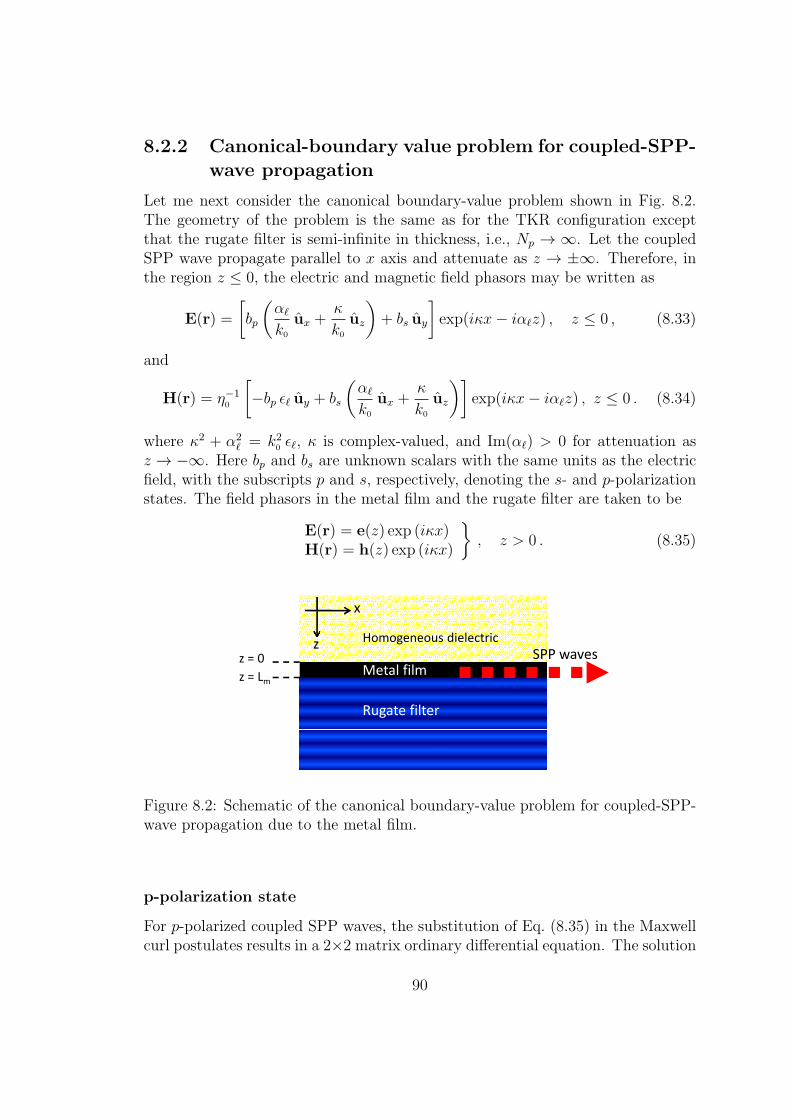
8.2.2 Canonical-boundary value problem for coupled-SPP-wave propagation
Let me next consider the canonical boundary-value problem shown in Fig. 8.2.The geometry of the problem is the same as for the TKR configuration exceptthat the rugate filter is semi-infinite in thickness, i.e., Np → ∞. Let the coupledSPP wave propagate parallel to x axis and attenuate as z → ±∞. Therefore, inthe region z ≤ 0, the electric and magnetic field phasors may be written as
E(r) =
[bp
(αℓ
k0
ux +κ
k0
uz
)+ bs uy
]exp(iκx− iαℓz) , z ≤ 0 , (8.33)
and
H(r) = η−10
[−bp ϵℓ uy + bs
(αℓ
k0
ux +κ
k0
uz
)]exp(iκx− iαℓz) , z ≤ 0 . (8.34)
where κ2 + α2ℓ = k20 ϵℓ, κ is complex-valued, and Im(αℓ) > 0 for attenuation as
z → −∞. Here bp and bs are unknown scalars with the same units as the electricfield, with the subscripts p and s, respectively, denoting the s- and p-polarizationstates. The field phasors in the metal film and the rugate filter are taken to be
E(r) = e(z) exp (iκx)H(r) = h(z) exp (iκx)
, z > 0 . (8.35)
Metal film
Rugate filter
SPP wavesz = 0
z = Lm
x
zHomogeneous dielectric
Figure 8.2: Schematic of the canonical boundary-value problem for coupled-SPP-wave propagation due to the metal film.
p-polarization state
For p-polarized coupled SPP waves, the substitution of Eq. (8.35) in the Maxwellcurl postulates results in a 2×2 matrix ordinary differential equation. The solution
90

of this equation in the metal film is[f (p) (Lm−)
]= exp
i[P (p)
mc
]Lm
·[f (p) (0+)
]. (8.36)
with [P (p)
mc
]=
[0 ωµ0 − κ2
ωϵ0ϵm
ωϵ0ϵm 0
]. (8.37)
The optical response of one period [1] of the rugate filter is given by a matrix[Q(p)
], defined via
[f (p) (Lm + 2Ω)
]=[Q(p)
]·[f (p) (Lm+)
], (8.38)
that has to be found using a piecewise uniform approximation. By virtue of the
Floquet–Lyapunov theorem [88], a matrix [Q(p)] can be defined such that
[Q(p)] = expi2Ω[Q
(p)]. (8.39)
Both [Q(p)] and [Q(p)] share the same eigenvectors, and their eigenvalues are also
related. Let [t](1) and [t](2), be the eigenvectors corresponding to the eigenvalues
σ1 and σ2, respectively, of [Q(p)]; then, the corresponding eigenvalue αn of [Q
(p)]
is given by
αn = −i lnσn2Ω
, n ∈ 1, 2 . (8.40)
After ensuring that Im(α1) > 0, I set
[f (p)(Lm+)] = cp [t](1) , (8.41)
where cp is an unknown scalar; the other eigenvalue of [Q(p)] pertains to a wave
that amplifies as z → ∞. The field at z = 0− can be written using Eqs. (8.33)and (8.34) as
[f (p)(0−)] = bp
[αℓ
k0
− ϵℓη0
]. (8.42)
Implementing the standard boundary conditions across the planes z = 0 andz = Lm, I arrive at the matrix equation
cp [t](1) = bp exp
i[P (p)
m,c
]Lm
·
[αℓ
k0
− ϵℓη0
](8.43)
91

by making the use of Eqs. (8.36), (8.41) and (8.42). Equation (8.43) can berearranged as [
M (p)]·[cpbp
]= [0] . (8.44)
For a nontrivial solution, the 2× 2 matrix [M (p)] must be singular, so that
det[M (p)
]= 0 (8.45)
is the required dispersion equation. This equation was solved for κ ∈ C using theNewton-Raphson method [89].
s-polarization state
The dispersion equation for s-polarized coupled SPP waves can be obtained in thesame way as in the foregoing subsection.
8.3 Numerical Results and Discussion
After finding the transmission and reflection amplitudes in the TKR configuration,two reflection coefficients
rpp = rp/ap , rss = rs/as , (8.46)
and two transmission coefficients
tpp = tp/ap , tss = ts/as , (8.47)
may be obtained. Now, the absorptances for p- and s-polarization states can bedefined as
Ap = 1−(|rpp|2 + |tpp|2
), As = 1−
(|rss|2 + |tss|2
), (8.48)
whereas Ap,s ∈ [0, 1] due to the principle of conservation of energy [70]. For allthe calculations reported in the remainder of this section, na = 1.45, nb = 2.32,and λ0 = 633 nm was fixed as in Ch. 3. The half-spaces z < 0 and z > LΣ weresupposed to be occupied by zinc selenide: nℓ = 2.58. The metal film was takenbe an aluminum thin film: ϵm = (0.75 + 3.9i)2 [44]. The half-period of the rugatefilter was taken to be Ω = 1.5λ0 because the interface of a semi-infinite metaland rugate filter can guide multiple p- and multiple s-polarized SPP waves at thisvalue of the half-period as was seen in Ch. 3. For the computation of absorptancesAp and As, the number of slices Nd were selected so as to have 2-nm-thick slices inLm < z < LΣ. The results for p-polarized SPP waves and s-polarized SPP wavesguided by the metal/rugate-filter in the TKR configuration of Sec. 8.2.1 are nowpresented and related to the results obtained from the solution of the canonicalboundary-value problem of Sec. 8.2.2.
92

8.3.1 p-polarization state
The variation of absorptance Ap vs. the angle of incidence θ is given in Fig. 8.3for Np ∈ 3, 4 and Lm = 30 nm. The absorptances were calculated for two valuesof Np in order to identify waveguide modes [104, 105], which must depend on Ld,as has been shown elsewhere [70,120]. A MathematicaTM program for calculatingAp versus θ is provided in Appendix B.5.
At seven values of the incidence angle θ, given in Table 8.1, a peak is presentindependent of the value of Np. The relative wavenumbers kx/k0 at these valuesof θ are also given in Table 8.1. The seven Ap-peaks in Fig. 8.3 represent theexcitation of p-polarized SPP waves because of the independence of their θ-valuefrom the value of Np. I arrived at the same conclusion from calculations madewith Np = 10 (not presented).
30 40 50 60 700.0
0.2
0.4
0.6
0.8
1.0
Θ HdegL
Ap
Figure 8.3: Absorptance Ap as function of the incidence angle θ in the TKRconfiguration, when λ0 = 633 nm, nℓ = 2.58, Lm = 30 nm, and Ω = 1.5λ0. Solidred line is for Np = 3 and dashed blue line is for Np = 4. Others parameters aregiven at the beginning of Sec. 8.3.
Now, the relative wavenumber of a p-polarized SPP wave that can be guidedby the prism/metal interface in the canonical configuration [34] is
κ/k0 =√ϵℓϵm/(ϵℓ + ϵm) = 3.2301 + 0.4091i , (8.49)
which is certainly not close to any of the relative wavenumbers given in Table 8.1.Therefore, any peak identified in Table 8.1 represents either an SPP wave guidedby the metal/rugate-filter interface or a coupled SPP wave guided by the metalfilm.
The variation of Ap with the thickness Lm of the metal film is illustrated inFig. 8.4 at the θ-values of the Ap-peaks for Np = 4. The value of Ap at eachpeak first increases and then decreases with the increase in the thickness of themetal film. This behavior is typical of the absorptance peak that represents the
93
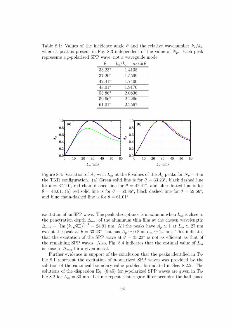
Table 8.1: Values of the incidence angle θ and the relative wavenumber kx/k0,where a peak is present in Fig. 8.3 independent of the value of Np. Each peakrepresents a p-polarized SPP wave, not a waveguide mode.
θ kx/k0 = nℓ sin θ
33.23 1.413837.20 1.559942.41 1.740048.01 1.917653.86 2.083659.66 2.226661.01 2.2567
(a)
0 10 20 30 40 50 600.0
0.2
0.4
0.6
0.8
1.0
Lm HnmL
Ap
(b)
0 10 20 30 40 50 600.0
0.2
0.4
0.6
0.8
1.0
Lm HnmL
Ap
Figure 8.4: Variation of Ap with Lm at the θ-values of the Ap-peaks for Np = 4 inthe TKR configuration. (a) Green solid line is for θ = 33.23, black dashed linefor θ = 37.20, red chain-dashed line for θ = 42.41, and blue dotted line is forθ = 48.01; (b) red solid line is for θ = 53.86, black dashed line for θ = 59.66,and blue chain-dashed line is for θ = 61.01.
excitation of an SPP wave. The peak absorptance is maximum when Lm is close tothe penetration depth ∆met of the aluminum thin film at the chosen wavelength:
∆met =[Im(k0
√ϵm)]−1
= 24.91 nm. All the peaks have Ap ≃ 1 at Lm ≃ 27 nmexcept the peak at θ = 33.23 that has Ap ≃ 0.8 at Lm ≃ 24 nm. This indicatesthat the excitation of the SPP wave at θ = 33.23 is not as efficient as that ofthe remaining SPP waves. Also, Fig. 8.4 indicates that the optimal value of Lm
is close to ∆met for a given metal.Further evidence in support of the conclusion that the peaks identified in Ta-
ble 8.1 represent the excitation of p-polarized SPP waves was provided by thesolution of the canonical boundary-value problem formulated in Sec. 8.2.2. Thesolutions of the dispersion Eq. (8.45) for p-polarized SPP waves are given in Ta-ble 8.2 for Lm = 30 nm. Let me repeat that rugate filter occupies the half-space
94

Table 8.2: Relative wavenumbers κ/k0 of p-polarized SPP waves obtained by thesolution of the canonical boundary-value problem formulated in Sec. 8.2.2 forLm = 30 nm. Other parameters are given at the beginning of Sec. 8.3.
p-pol 1.4125 + 0.0004i 1.5600 + 0.0008i 1.7401 + 0.0013i1.9175 + 0.0015i 2.0836 + 0.0018i 2.2302 + 0.0173i2.2498 + 0.0079i
z > Lm in that canonical boundary-value problem instead of having a finite thick-ness Ld = 2ΩNp as for the TKR configuration.
All solutions of the canonical boundary-value problem represent SPP waves.Depending on the thickness of the metal film, these SPP waves can either couplethe two interfaces of the metal film or not. The relative wavenumbers κ/k0 ofthe seven possible p-polarized solutions are given in Table 8.2. Comparison ofTables 8.1 and 8.2 shows that Re [κ/k0] of each item in Table 8.2 is close to therelative wavenumber kx/k0 at one of the Ap-peaks, signifying thereby that theseven peaks identified in Table 8.1 represent the excitation of p-polarized SPPwaves.
To analyze the spatial power-density profiles of the SPP waves excited byan incident p-polarized plane wave in the TKR configuration, I have shown thevariation of the Cartesian components of time-averaged Poynting vector
P(x, z) =1
2Re [E(x, z)×H∗(x, z)] (8.50)
in Fig. 8.5 for θ = 33.21, 42.41, and 59.66 along a line normal to the planez = Lm; P(x, z) ≡ P(z) as kx ∈ R. The figure shows that Pz decays in the metalfilm as z → Lm and is negligible in the rugate filter (z > Lm). This should beexpected because the incident plane wave decays as it penetrates into the metal.However, Px is localized to the metal/rugate-filter interface and decays away fromthat interface on both sides. The localization of the Px to the interface planez = Lm is a clear indicator of an SPP wave. Le me note that, while the variationof Px is similar in the metal for the three SPP waves, the spatial profiles of Px
in the rugate filter are different for different SPP waves, indicating the differentdegree of localization of the SPP wave excited with a different value of θ.
In all the plots presented in Fig. 8.5, Px(z = 0) = 0, whereas Px(z = LΣ) ≃ 0.For all other SPP waves excited by p-polarized incident plane waves, the samebehavior of Px and Pz was noted (profiles not shown). Because the thickness ofthe metal film is almost equal to the penetration depth of the metal, Px doesnot decay to zero in the thin metal film. For a sufficiently thick metal film, allthe power density may reside completely in the rugate filter and the metal film;however, no SPP waves may be excited in the TKR configuration if the metal filmis made too thick.
95

0.0 0.2 0.4 0.6 0.8 1.0-0.004-0.002
0.0000.0020.004
z Lm
P8x
,z<
0 2 4 6 80.0000.0050.0100.0150.020
Hz-LmLW
P8x
,z<
0.0 0.2 0.4 0.6 0.8 1.0-0.004-0.002
0.0000.0020.004
z Lm
P8x
,z<
0 1 2 3 40.000.010.020.030.04
Hz-LmLW
P8x
,z<
0.0 0.2 0.4 0.6 0.8 1.0-0.004-0.002
0.0000.0020.004
z Lm
P8x
,z<
0.0 0.5 1.0 1.5 2.00.0000.0020.0040.0060.008
Hz-LmLW
P8x
,z<
Figure 8.5: Variations of the Cartesian components Px and Pz (in W m−2) ofthe time-averaged Poynting vector along the z axis in (left) the metal film and(right) the rugate filter for Lm = 30 nm in the TKR configuration for a p-polarizedincident plane wave (ap = 1 V m−1, as = 0). (top) θ = 33.23, (middle) θ = 42.41,and (bottom) θ = 59.66. Red solid line represents Px, blue dashed line representsPz, and Py is identically zero.
The thin metal film in the TKR configuration, however, may lead to thecoupling of the two interface, that is, an SPP wave may be coupled to bothprism/metal and metal/rugate-filter interfaces, or an SPP wave may be excitedon the metal/rugate-filter interface. To distinguish between coupled and uncou-pled p-polarized SPP waves, the spatial power-density profiles of the SPP wavesguided by the thin metal film were examined. Representative spatial profiles ofpower density for two different p-polarized SPP waves are given in Fig. 8.6 for thecanonical boundary-value problem formulated in Sec. 8.2.2. The SPP wave withκ/k0 = 1.4125+ 0.0004i is loosely localized to prism/metal interface in the prism.However, the SPP wave with κ/k0 = 2.2302+0.0173i is strongly localized to boththe prism/metal and the metal/rugate-filter interfaces. The spatial power densityprofiles (not shown) of the remaining p-polarized SPP waves showed that all the
96

-6 -5 -4 -3 -2 -1 00.0000.0050.0100.0150.0200.025
zW
P8x
,z<
-6 -5 -4 -3 -2 -1 00.0000.0050.0100.0150.0200.025
zW
P8x
,z<
0.0 0.2 0.4 0.6 0.8 1.0-0.04
-0.02
0.00
0.02
0.04
zLm
P8x
,z<
0.0 0.2 0.4 0.6 0.8 1.0-0.04
-0.02
0.00
0.02
0.04
zLm
P8x
,z<
0 2 4 6 80.0
0.1
0.2
0.3
0.4
Hz-LmLW
P8x
,z<
0.0 0.5 1.0 1.5 2.00.00
0.05
0.10
0.15
0.20
Hz-LmLW
P8x
,z<
Figure 8.6: Variations of the Cartesian components of the time-averaged Poyntingvector P(x = 0, z) (in W m−2) along the z axis in (top) the prism material,(middle) the metal film with Lm = 30 nm, and (bottom) the rugate filter for thecanonical boundary-value problem formulated in Sec. 8.2.2 for a p-polarized SPPwave with (left) κ/k0 = 1.4125+0.0004i, and (right) κ/k0 = 2.2302+0.0173i. Redsolid line represents Px, blue dashed line represents Pz, and Py is identically zero.The computations were made with bp = 1 V m−1.
SPP waves are strongly localized to both the interfaces except the two SPP waveswith κ/k0 = 1.4125 + 0.0004i and κ/k0 = 1.5600 + 0.0008i; however, most of thepower density of each p-polarized SPP waves resides in the rugate filter. So, fiveout of the seven p-polarized SPP waves are coupled SPP waves.
To see if the coupling due to thin metal film results in new SPP waves inrelation to SPP waves guided by the metal/rugate-filter interface, the canonicalboundary-value problem of SPP-wave propagation by that interface was solved.The relative wavenumbers κ/k0 of seven possible p-polarized SPP waves that areguided by that interface are presented in Table 8.3. All the p-polarized SPP wavesthat are excited in the TKR configuration are also guided by the interface of semi-infinite metal and rugate filter. This shows that the coupling of the two interfaces
97
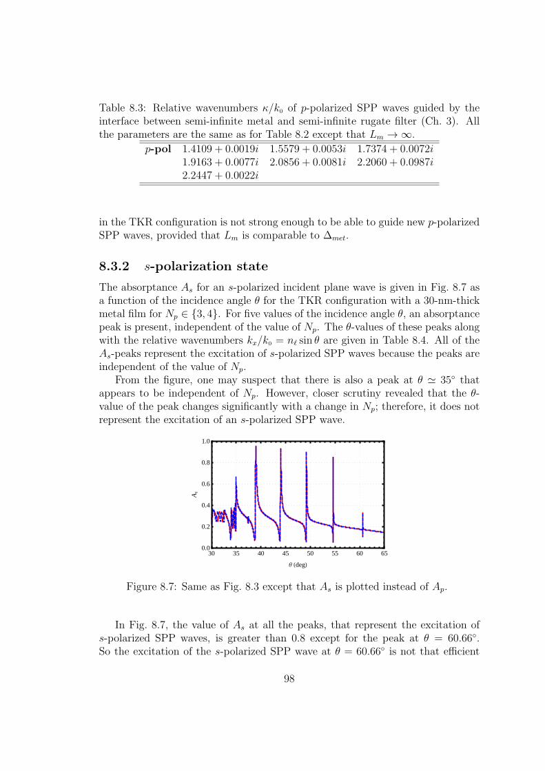
Table 8.3: Relative wavenumbers κ/k0 of p-polarized SPP waves guided by theinterface between semi-infinite metal and semi-infinite rugate filter (Ch. 3). Allthe parameters are the same as for Table 8.2 except that Lm → ∞.
p-pol 1.4109 + 0.0019i 1.5579 + 0.0053i 1.7374 + 0.0072i1.9163 + 0.0077i 2.0856 + 0.0081i 2.2060 + 0.0987i2.2447 + 0.0022i
in the TKR configuration is not strong enough to be able to guide new p-polarizedSPP waves, provided that Lm is comparable to ∆met.
8.3.2 s-polarization state
The absorptance As for an s-polarized incident plane wave is given in Fig. 8.7 asa function of the incidence angle θ for the TKR configuration with a 30-nm-thickmetal film for Np ∈ 3, 4. For five values of the incidence angle θ, an absorptancepeak is present, independent of the value of Np. The θ-values of these peaks alongwith the relative wavenumbers kx/k0 = nℓ sin θ are given in Table 8.4. All of theAs-peaks represent the excitation of s-polarized SPP waves because the peaks areindependent of the value of Np.
From the figure, one may suspect that there is also a peak at θ ≃ 35 thatappears to be independent of Np. However, closer scrutiny revealed that the θ-value of the peak changes significantly with a change in Np; therefore, it does notrepresent the excitation of an s-polarized SPP wave.
30 35 40 45 50 55 60 650.0
0.2
0.4
0.6
0.8
1.0
Θ HdegL
As
Figure 8.7: Same as Fig. 8.3 except that As is plotted instead of Ap.
In Fig. 8.7, the value of As at all the peaks, that represent the excitation ofs-polarized SPP waves, is greater than 0.8 except for the peak at θ = 60.66.So the excitation of the s-polarized SPP wave at θ = 60.66 is not that efficient
98

Table 8.4: Values of the incidence angles θ, and the relative wavenumbers kx/k0,where a peak is present in Fig. 8.7 independent of the value of Np.
θ kx/k0 = nℓ sin θ
38.97 1.622644.01 1.792549.22 1.953654.63 2.103860.66 2.2491
as those of the rest of the s-polarized SPP waves. Moreover, the comparison ofFigs. 8.3 and 8.7 shows that the peaks representing the excitation of s-polarizedSPP waves are narrower than those representing the excitation of p-polarized SPPwaves.
0 10 20 30 40 50 600.0
0.2
0.4
0.6
0.8
1.0
Lm HnmL
As
Figure 8.8: Variation of As vs. the thickness of the metal film Lm at the θ-position of the As-peaks for Np = 3 in the TKR configuration. Solid red line isfor θ = 38.97, black dashed line for θ = 44.01, blue chain-dashed for θ = 49.22,green dotted line for θ = 54.63, and orange dashed line (with larger dashes) isfor θ = 60.66.
To analyze the effect of the metal film’s thickness on the coupling efficiency,the variation of As vs. Lm is given in Fig. 8.8 for θ-values of all five As-peaks ofinterest. The graphs show that As reaches a maximum value close to Lm = 27 nm(the same value as for p-polarized incident plane waves) for all θ-values except forθ = 60.66. The maximum of the As-peak at θ = 60.66 occurs at Lm ≃ 12 nm;however, at Lm = 12 nm the value of As for other four As-peaks is less than0.4. Therefore, to excite maximum number of s-polarized SPP waves efficiently, avalue of Lm close to 27 nm should be used. This is in contrast to the excitation
99

of p-polarized SPP waves, where all possible SPP waves can be excited efficientlyusing a metal film with Lm = 27 nm.
The solution of the dispersion equation for s-polarized SPP waves guided bythe metal film, with the semi-infinite prism on one side and the semi-infinite rugatefilter on the other, are presented in Table 8.4. The value of Re [κ/k0] of each itemin Table 8.5 is close to the relative wavenumber kx/k0 at one of the As-peaksgiven in Table 8.4, reinforcing the conclusion that the peaks identified in Table 8.4represent the excitation of s-polarized SPP waves in the TKR configuration.
Table 8.5: Same as Table 8.2 except that the relative wavenumbers of s-polarizedSPP waves are given instead of p-polarized SPP waves.
s-pol 1.6226 + 0.0010i 1.7924 + 0.0008i 1.9534 + 0.0004i2.1038 + 0.0001i 2.2490 + 1.0136× 10⁻⁵i
0.0 0.2 0.4 0.6 0.8 1.00.0000.0020.0040.0060.008
z Lm
P8x
,z<
0 1 2 3 40.000.050.100.150.20
Hz-LmLW
P8x
,z<
0.0 0.2 0.4 0.6 0.8 1.00.0000
0.0005
0.0010
0.0015
z Lm
P8x
,z<
0 1 2 3 40.00.20.40.60.81.0
Hz-LmLW
P8x
,z<
Figure 8.9: Variations of the Cartesian components Px and Pz (in W m−2) of thetime-averaged Poynting vector along the z axis in (left) the metal film and (right)the rugate filter for Lm = 30 nm in the TKR configuration for an s-polarizedincident plane wave (ap = 0, as = 1 V m−1). (top) θ = 49.22, and (bottom)θ = 60.66. Red solid line represents Px, blue dashed line represents Pz, and Py isidentically zero.
Representative spatial profiles of the power density for two s-polarized SPPwaves are provided in Fig. 8.9 in the TKR configuration for θ = 49.22 and 60.66.For both the cases, Pz decays in the metal film as z → Lm and is negligible in therugate filter, as was the case for p-polarized incident plane wave. In the rugate
100

-6 -5 -4 -3 -2 -1 00.000
0.001
0.002
0.003
0.004
zW
P8x
,z<
-6 -5 -4 -3 -2 -1 00.000
0.001
0.002
0.003
0.004
zW
P8x
,z<
0.0 0.2 0.4 0.6 0.8 1.0-0.005
0.000
0.005
0.010
0.015
zLm
P8x
,z<
0.0 0.2 0.4 0.6 0.8 1.0-0.005
0.000
0.005
0.010
0.015
zLm
P8x
,z<
0.0 0.5 1.0 1.5 2.00.0
0.2
0.4
0.6
0.8
Hz-LmLW
P8x
,z<
0.0 0.5 1.0 1.5 2.00
1020304050
Hz-LmLW
P8x
,z<
Figure 8.10: Variations of the Cartesian components of the time-averaged Poyntingvector P(x = 0, z) (in W m−2) along the z axis in (top) the prism material,(middle) the metal film with Lm = 30 nm, and (bottom) the rugate filter fortwo s-polarized SPP waves obtained from the solution of the canonical boundary-value problem shown in Fig. 8.2. (left) κ/k0 = 1.9534+0.0004i, and (right) κ/k0 =2.2490 + 1.0136× 10⁻⁵i. Red solid line represents Px, blue dashed line representsPz, and Py is identically zero. The computations were made with bs = 1 Vm−1.
Table 8.6: Same as Table 8.3 except that the relative wavenumbers of s-polarizedSPP waves are given instead of p-polarized SPP waves.
s-pol 1.6205 + 0.0018i 1.7910 + 0.0012i 1.9528 + 0.0006i2.1037 + 0.0001i 2.2490 + 1.1021× 10⁻⁵i
filter, Px is confined to within one period 2Ω of the rugate filter for both s-polarizedSPP waves. For θ = 49.22, Px decays away from the interface in the metal film.However, for θ = 60.66, Px decays away from the interface at z = Lm but againstarts to amplify as z → 0, indicating that the SPP wave is not only guided by theinterface at z = Lm but may also be coupled to the interface at z = 0. The spatial
101

profiles of the power density of s-polarized SPP waves at θ = 38.97, 44.01, and54.63 were similar to that of the s-polarized SPP wave at θ = 49.22 (profiles notshown).
The spatial profiles of the power density of s-polarized SPP waves were exam-ined to see if the s-polarized SPP waves are coupled for the canonical boundary-value problem formulated in Sec. 8.2.2. Representative spatial profiles for twos-polarized SPP waves guided by the metal thin film with a semi-infinite rugatefilter on one side and a semi-infinite prism on the other side are given in Fig. 8.10for κ/k0 = 1.9534 + 0.0004i and 2.2490 + 1.10136 × 10⁻⁵i. The parameters forthe prism, the metal film, and the rugate filter are the same as for the TKR con-figuration. These two SPP waves correspond to the two SPP waves in Fig. 8.9.The spatial profiles (not shown) for the rest of s-polarized SPP waves of thecanonical boundary-value problem, are also similar to those shown in Fig. 8.10.Both profiles show that the s-polarized SPP waves are strongly localized to themetal/rugate-filter interface and very loosely localized to the prism/metal inter-face, indicating that the s-polarized SPP waves are not coupled. This is in contrastto the p-polarization state, where five of the seven SPP waves are coupled to bothinterfaces.
The canonical boundary-value problem of SPP-wave propagation by the inter-face of a semi-infinite metal and the semi-infinite rugate filter (Ch. 3) was solvedfor the s-polarization state, and the relative wavenumbers κ/k0 of five s-polarizedSPP waves are given in Table 8.6. The wavenumbers in Tables 8.5 and 8.6 arealmost the same, so the coupling due to the thin metal film has not resultedin new s-polarized SPP waves in TKR configuration, as was also the case withp-polarization state.
8.4 Concluding Remarks
The plane waves of either p- or s-polarization state, propagating in an opticallydenser dielectric material, were made incident on a metal-capped rugate filter. Theabsorptances were calculated using a stable algorithm as functions of the incidenceangle. The excitation of SPP waves was inferred from the presence of those peaksin the absorptance spectrum that were independent of the thickness of the rugatefilter. It was concluded that
(i) multiple p- and s-polarized SPP waves can be excited using the TKR con-figuration,
(ii) most of the possible SPP waves can be excited efficiently using a metal filmwith a thickness that is close to the penetration depth, and
(iii) the absorptance peaks representing the excitation of s-polarized SPP wavesare narrower than those representing p-polarized SPP waves.
102
A canonical boundary-value problem to study the propagation of coupled SPPwaves by a metal film, with a semi-infinite rugate filter on one side and a semi-infinite homogeneous dielectric material on the other side, was also formulated toobtain a dispersion equation for each of the two linear polarization states. Thesolution of the dispersion equations and the spatial profiles of the SPP waves
(i) reinforced the results of the TKR configuration, and
(ii) showed that p-polarized SPP waves are more likely to be coupled to both theprism/metal and metal/rugate-filter interfaces than s-polarized SPP waves.
However, the solution of another canonical boundary-value problem (Ch. 3) ofSPP-wave propagation by the interface of a semi-infinite metal and a semi-infiniterugate filter revealed that the coupling due to the thin metal film in the TKRconfiguration does not result in new SPP waves.
103

Chapter 9
Grating-Coupled Excitation ofMultiple SPP Waves Guided byMetal/Rugate-Filter Interface‡
9.1 Introduction
The canonical boundary-value problem solved in Ch. 3 showed that multipleSPP waves can be guided even if the dielectric partnering material is isotropic—provided that the material is also periodically nonhomogeneous normal to theinterface. This is a very attractive result, because both partnering materials areisotropic and because the dielectric partnering material can be fabricated as arugate filter [2, 76,78,80,110].
In Ch. 8, I presented the investigations on the prism-coupled (TKR configu-ration) excitation of multiple SPP waves. It was seen in that chapter that theabsorptance peaks independent of the thickness of the dielectric layer representthe excitation of SPP waves. For this chapter, I set out to investigate the exci-tation of multiple SPP waves by the periodically corrugated interface of a metaland a rugate filter, which is an alternative to the TKR configuration. Though theTKR configuration is easier to implement in a laboratory than the grating-coupledconfiguration, it does not allow the application of multiple SPP waves in the solarcells. However, as is shown in Ch. 10, the grating-coupled configuration can beused to enhance the absorption of light in thin-film solar cells. In the grating-coupled configuration, fields in the two partnering materials are represented as alinear superposition of Floquet harmonics. If the component of the wavevector ofa Floquet harmonic in the plane of the grating is the same as that of the SPPwave, the Floquet harmonic can couple with the SPP wave. The interplay of theperiodic nonhomogeneity of the dielectric partnering material and a periodically
‡This chapter is based on: M. Faryad and A. Lakhtakia, “Grating-coupled excitation ofmultiple surface-plasmon-polariton waves,” Phys. Rev. A 84, 033852 (2011).
104
corrugated interface is phenomenologically rich [111, 112], and should lead to theexcitation of multiple SPP waves as different Floquet harmonics.
The relevant boundary-value problem was formulated using the rigorous coupled-wave approach (RCWA) [106, 118]. In this numerical technique, the constitutiveparameters are expanded in terms of Fourier series with known expansion coef-ficients, and the electromagnetic field phasors are expanded in terms of Floquetharmonics whose coefficients are determined by substitution in the frequency-domain Maxwell curl postulates. The accuracy of solution is conventionally heldto depend only on the number of Floquet harmonics actually used in the com-putations [107]. The RCWA has been used to solve for scattering by a varietyof surface-relief gratings [106–108, 119], generally with both partnering materialsbeing homogeneous. The theoretical formulation of the boundary-value problem isprovided in Sec. 9.2 and the numerical results are discussed in Sec. 9.3. Concludingremarks are presented in Sec. 9.4.
9.2 Boundary-Value Problem
9.2.1 Description
Let me consider the boundary-value problem shown schematically in Fig. 9.1.The regions z < 0 and z > d3 are vacuous, the region 0 ≤ z ≤ d1 is occupied bythe dielectric partnering material with relative permittivity ϵd(z), and the regiond2 ≤ z ≤ d3 by the metallic partnering material with spatially uniform relativepermittivity ϵm. The region d1 < z < d2 contains a surface-relief grating of periodL along the x axis. The relative permittivity ϵg(x, z) = ϵg(x± L, z) in this regionis taken to be as
ϵg(x, z) =
ϵm − [ϵm − ϵd(z)]U [d2 − z − g(x)] , x ∈ (0, L1) ,
ϵd(z) , x ∈ (L1, L) ,(9.1)
for z ∈ (d1, d2), with
g(x) = (d2 − d1) sin
(πx
L1
), L1 ∈ (0, L) , (9.2)
and
U(ζ) =
1 , ζ ≥ 0 ,
0 , ζ < 0 .(9.3)
The depth of the surface-relief grating defined by Eq. (9.2) is d2 − d1. This par-ticular grating shape is chosen for the ease of fabrication; however, the theoreticalformulation given in the remainder of this section is independent of the shape ofthe surface-relief grating.
105
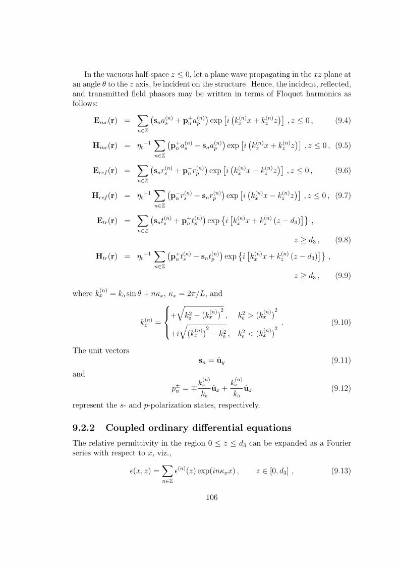
In the vacuous half-space z ≤ 0, let a plane wave propagating in the xz plane atan angle θ to the z axis, be incident on the structure. Hence, the incident, reflected,and transmitted field phasors may be written in terms of Floquet harmonics asfollows:
Einc(r) =∑n∈Z
(sna
(n)s + p+
n a(n)p
)exp
[i(k(n)x x+ k(n)z z
)], z ≤ 0 , (9.4)
Hinc(r) = η0−1∑n∈Z
(p+n a
(n)s − sna
(n)p
)exp
[i(k(n)x x+ k(n)z z
)], z ≤ 0 , (9.5)
Eref (r) =∑n∈Z
(snr
(n)s + p−
n r(n)p
)exp
[i(k(n)x x− k(n)z z
)], z ≤ 0 , (9.6)
Href (r) = η0−1∑n∈Z
(p−n r
(n)s − snr
(n)p
)exp
[i(k(n)x x− k(n)z z
)], z ≤ 0 , (9.7)
Etr(r) =∑n∈Z
(snt
(n)s + p+
n t(n)p
)exp
i[k(n)x x+ k(n)z (z − d3)
],
z ≥ d3 , (9.8)
Htr(r) = η0−1∑n∈Z
(p+n t
(n)s − snt
(n)p
)exp
i[k(n)x x+ k(n)z (z − d3)
],
z ≥ d3 , (9.9)
where k(n)x = k0 sin θ + nκx, κx = 2π/L, and
k(n)z =
+
√k20 − (k
(n)x )
2, k20 > (k
(n)x )
2
+i
√(k
(n)x )
2− k20 , k20 < (k
(n)x )
2. (9.10)
The unit vectorssn = uy (9.11)
and
p±n = ∓k(n)z
k0
ux +k(n)x
k0
uz (9.12)
represent the s- and p-polarization states, respectively.
9.2.2 Coupled ordinary differential equations
The relative permittivity in the region 0 ≤ z ≤ d3 can be expanded as a Fourierseries with respect to x, viz.,
ϵ(x, z) =∑n∈Z
ϵ(n)(z) exp(inκxx) , z ∈ [0, d3] , (9.13)
106
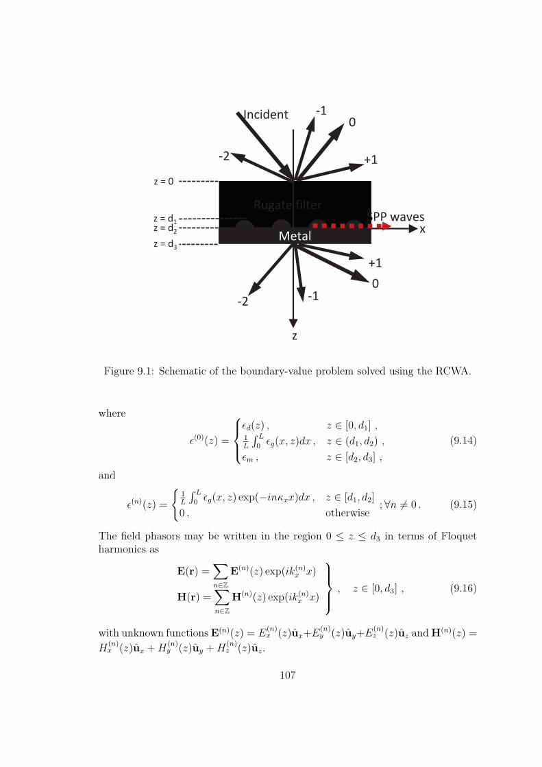
SPP waves Rugate filter
Metal
Incident
z
x
z = 0
z = d1 z = d2
z = d3
Metal
0
+1
-1
-2
0
+1
-1 -2
Figure 9.1: Schematic of the boundary-value problem solved using the RCWA.
where
ϵ(0)(z) =
ϵd(z) , z ∈ [0, d1] ,1L
∫ L
0ϵg(x, z)dx , z ∈ (d1, d2) ,
ϵm , z ∈ [d2, d3] ,
(9.14)
and
ϵ(n)(z) =
1L
∫ L
0ϵg(x, z) exp(−inκxx)dx , z ∈ [d1, d2]
0 , otherwise; ∀n = 0 . (9.15)
The field phasors may be written in the region 0 ≤ z ≤ d3 in terms of Floquetharmonics as
E(r) =∑n∈Z
E(n)(z) exp(ik(n)x x)
H(r) =∑n∈Z
H(n)(z) exp(ik(n)x x)
, z ∈ [0, d3] , (9.16)
with unknown functionsE(n)(z) = E(n)x (z)ux+E
(n)y (z)uy+E
(n)z (z)uz andH(n)(z) =
H(n)x (z)ux +H
(n)y (z)uy +H
(n)z (z)uz.
107

Substitution of Eqs. (9.13) and (9.16) in the frequency-domain Maxwell curlpostulates results in a system of four ordinary differential equations and two alge-braic equations as follows:
d
dzE(n)
x (z)− ik(n)x E(n)z (z) = ik0η0H
(n)y (z) , (9.17)
d
dzE(n)
y (z) = −ik0η0H(n)x (z) , (9.18)
k(n)x E(n)y (z) = k0η0H
(n)z (z) , (9.19)
d
dzH(n)
x (z)− ik(n)x H(n)z (z) = − ik0
η0
∑m∈Z
ϵ(n−m)(z)E(m)y (z) , (9.20)
d
dzH(n)
y (z) =ik0
η0
∑m∈Z
ϵ(n−m)(z)E(m)x (z) , (9.21)
k(n)x H(n)y (z) = −k0
η0
∑m∈Z
ϵ(n−m)(z)E(m)z (z) . (9.22)
Equations (9.17)–(9.22) hold ∀z ∈ (0, d3) and ∀n ∈ Z. These equations can berecast into an infinite system of coupled first-order ordinary differential equations.This system can not be implemented on a digital computer. Therefore, |n| ≤ Nt
was restricted and then define the column (2Nt + 1)-vectors
[Xσ(z)] = [X(−Nt)σ (z), X(−Nt)
σ (z), ..., X(0)σ (z), ..., X(Nt−1)
σ (z), X(Nt)σ (z)]T , (9.23)
for X ∈ E,H and σ ∈ x, y, z. Similarly, let me define (2Nt + 1)× (2Nt + 1)-matrixes
[Kx] = diag[k(n)x ] , [ϵ(z)] =
[ϵ(n−m)(z)
], (9.24)
where diag[k(n)x ] is a diagonal matrix.
Equations (9.19) and (9.22) yield
[Ez(z)] = −η0
k0
[ϵ(z)
]−1 ·[K
x
]· [Hy(z)] (9.25)
and
[Hz(z)] =1
η0k0
[K
x
]· [Ey(z)] , (9.26)
the use of which in Eqs. (9.17), (9.18), (9.20) and (9.21) eliminates E(n)z and
H(n)z ∀n ∈ Z, and gives the matrix ordinary differential equation
d
dz[f(z)] = i
[P (z)
]· [f(z)] , z ∈ (0, d3) , (9.27)
108

where the column vector [f(z)] with 4(2Nt + 1) components is defined as
[f(z)] =[[Ex(z)]
T , [Ey(z)]T , η0 [Hx(z)]
T , η0 [Hy(z)]T]T
(9.28)
and the 4(2Nt + 1)× 4(2Nt + 1)-matrix[P (z)
]is given by
[P (z)
]=
[0] [
0] [
0] [
P14(z)][
0] [
0]
−k0
[I] [
0][
0] [
P32(z)] [
0] [
0][
P41(z)] [
0] [
0] [
0]
, (9.29)
where[0]is the (2Nt+1)×(2Nt+1) null matrix and
[I]is the (2Nt+1)×(2Nt+1)
identity matrix, the three nonnull submatrixes on the right side of Eq. (9.29) areas follows: [
P14(z)]
= k0
[I]− 1
k0
[K
x
]·[ϵ(z)
]−1 ·[K
x
], (9.30)[
P32(z)]
=1
k0
[K
x
]2− k0
[ϵ(z)
], (9.31)[
P41(z)]
= k0
[ϵ(z)
]. (9.32)
9.2.3 Solution algorithm
The column vectors [f(0)] and [f(d3)] can be written using Eqs. (9.4)–(9.9) as
[f(0)] =
[Y +
e
] [Y −
e
][Y +
h
] [Y −
h
] ·[[A][R]
], [f(d3)] =
[Y +
e
][Y +
h
] · [T] , (9.33)
where
[A] =[a(−Nt)s , a(−Nt+1)
s , ..., a(0)s , ..., a(Nt−1)s , a(Nt)
s ,
a(−Nt)p , a(−Nt+1)
p , ..., a(0)p , ..., a(Nt−1)p , a(Nt)
p
]T, (9.34)
[R] =[r(−Nt)s , r(−Nt+1)
s , ..., r(0)s , ..., r(Nt−1)s , r(Nt)
s ,
r(−Nt)p , r(−Nt+1)
p , ..., r(0)p , ..., r(Nt−1)p , r(Nt)
p
]T, (9.35)
[T] =[t(−Nt)s , t(−Nt+1)
s , ..., t(0)s , ..., t(Nt−1)s , t(Nt)
s ,
t(−Nt)p , t(−Nt+1)
p , ..., t(0)p , ..., t(Nt−1)p , t(Nt)
p
]T, (9.36)
109

and the nonzero entries of (4Nt + 2)× (4Nt + 2)-matrixes[Y ±
e,h
]are as follows:(
Y ±e
)nm
= 1 , n = m+ 2Nt + 1 , (9.37)(Y ±e
)nm
= ∓k(n)z
k0, n = m− 2Nt − 1 , (9.38)(
Y ±h
)nm
= ∓k(n)z
k0, n = m ∈ [1, 2Nt + 1] , (9.39)(
Y ±h
)nm
= −1 , n = m ∈ [2Nt + 2, 4Nt + 2] . (9.40)
In order to devise a stable algorithm [106–109], the region 0 ≤ z ≤ d1 is dividedinto Nd slices and the region d1 < z < d2 into Ng slices, but the region d2 ≤ z ≤ d3is kept as just one slice. So, there are Nd+Ng+1 slices and Nd+Ng+2 interfaces.In the jth slice, j ∈ [1, Nd +Ng + 1], bounded by the planes z = zj−1 and z = zj,I approximate
[P (z)
]=[P]j=
[P
(zj + zj−1
2
)], z ∈ (zj, zj−1) , (9.41)
so that Eq. (9.27) yields
[f(zj−1)] =[G]j· exp
−i∆j
[D]j
·[G]−1
j· [f(zj)] , (9.42)
where ∆j = zj − zj−1,[G]jis a square matrix comprising the eigenvectors of
[P]j
as its columns, and the diagonal matrix[D]jcontains the eigenvalues of
[P]jin
the same order.Let me define auxiliary column vectors [T]j and auxiliary transmission matrixes[
Z]jby the relation [108]
[f(zj)] =[Z]j· [T]j , j ∈ [0, Nd +Ng + 1] , (9.43)
where z0 = 0,
[T]Nd+Ng+1 = [T] , and[Z]Nd+Ng+1
=
[Y +
e
][Y +
h
] . (9.44)
To find [T]j and[Z]jfor j ∈ [0, Nd +Ng], I substitute Eq. (9.43) in (9.42), which
results in the relation[Z]j−1
· [T]j−1 =[G]j·[e−i∆j [D]uj 0
0 e−i∆j [D]lj
]·[G]−1
j·[Z]j· [T]j ,
j ∈ [1, Nd +Ng + 1] , (9.45)
110
where[D]ujand
[D]ljare the upper and lower diagonal submatrixes of
[D]j, re-
spectively, when the eigenvalues are arranged in decreasing order of the imaginarypart.
Since [T]j and[Z]jcannot be determined simultaneously from Eq. (9.45), let
me define [108]
[T]j−1 = exp−i∆j
[D]uj
·[W]uj· [T]j , (9.46)
where the square matrix[W]ujand its counterpart
[W]ljare defined via[ [
W]uj[
W]lj
]=[G]−1
j·[Z]j. (9.47)
Substitution of Eq. (9.46) in (9.45) results in the relation
[Z]j−1
=[G]j·
[ [I]
exp−i∆j[D]lj
·[W]lj·[W]uj
−1
· expi∆j[D]uj
] ,j ∈ [1, Nd +Ng + 1] . (9.48)
From Eqs. (9.47) and (9.48), I find[Z]0in terms of
[Z]Nd+Ng+1
. After partitioning
[Z]0=
[ [Z]u0[
Z]l0
], (9.49)
and using Eqs. (9.33) and (9.43), [R] and [T]0 are found as follows:
[[T]0[R]
]=
[Z]u0 −[Y −
e
][Z]l0
−[Y −
h
] −1
·
[Y +
e
][Y +
h
] · [A] . (9.50)
Equation (9.50) is obtained by enforcing the usual boundary conditions acrossthe plane z = 0. After [T]0 is known, [T] = [T]Nd+Ng+1 is found by reversing the
sense of iterations in Eq. (9.46).
9.3 Numerical Results and Discussion
9.3.1 Homogeneous dielectric partnering material
Let me begin with the dielectric partnering material being homogeneous, i.e., ϵd(z)is independent of z. This case has been numerically illustrated by Homola [34,p. 38] and I adopted the same parameters: λ0 = 800 nm, ϵd = 1.766 (water),
111

ϵm = −25+ 1.44i (gold), and L = 672 nm. The incident plane wave is p polarized
(a(n)p = δn0 V m−1 and a
(n)s ≡ 0 ∀n ∈ Z) and the quantity of importance is the
absorptance
Ap = 1−Nt∑
n=−Nt
(∣∣r(n)s
∣∣2 + ∣∣r(n)p
∣∣2 + ∣∣t(n)s
∣∣2 + ∣∣t(n)p
∣∣2)Re(k(n)z
k(0)z
), (9.51)
which simplifies to
Ap = 1−Nt∑
n=−Nt
(∣∣r(n)p
∣∣2 + ∣∣t(n)p
∣∣2)Re(k(n)z
k(0)z
), (9.52)
because all materials are isotropic.Figure 9.2(a) shows the variation of Ap versus the incidence angle θ for a
sinusoidal surface-relief grating defined by [34]
g(x) =1
2(d2 − d1)
[1 + sin
(2πx
L
)](9.53)
instead of Eq. (9.2), and Fig. 9.2(b) shows the same for the surface-relief grat-ing defined by Eq. (9.2) with L1 = 0.5L. For computational purposes, I setNd = 1, Ng = 50, and Nt = 10, after ascertaining that all nonzero reflectances∣∣∣r(n)p
∣∣∣2 Re(k(n)z /k(0)z
)and transmittances
∣∣∣t(n)p
∣∣∣2 Re(k(n)z /k(0)z
)converged within
±0.5% for all n ∈ [−Nt, Nt].Each figure shows plots of Ap vs. θ for three different values of the thickness
d1, in order to distinguish [70] between
(i) surface waves, which must be independent of d1 for sufficiently large valuesof that parameter, and
(ii) waveguide modes [104,105], which must depend on d1,
as has been shown in Ref. 120 and in Ch. 7. In both figures, an absorptancepeak at θ ≃ 12.5 for all three values of d1 indicates the excitation of an SPPwave. Parenthetically, I note here that an SPP wave is a solution of a canonicalboundary-value problem involving the planar interface of two semi-infinite halfspaces, one of which is occupied by a metal and the other by a dielectric material;but, as the canonical boundary-value problem cannot be implemented practically,both materials must be present as sufficiently thick layers in a real situation sothat the SPP wave decays appreciably through the thickness of each layer.
The relative wavenumbers k(n)x /k0 of a few Floquet harmonics at θ = 12.5 are
given in Table 9.1. The solution of the canonical boundary-value problem [34]
112

0 5 10 15 20 250.0
0.2
0.4
0.6
0.8
1.0
0 5 10 15 20 250.0
0.2
0.4
0.6
0.8
1.0
A p(a)
(b)
A p
(deg)
Figure 9.2: Absorptance Ap as a function of the incidence angle θ when the surface-relief grating is defined by either (a) Eq. (9.53) or (b) Eq. (9.2). Black squaresrepresent d1 = 1500 nm, red circles d1 = 1000 nm, and blue triangles d1 = 800 nm.The grating depth (d2 − d1 = 50 nm) and the thickness of the metallic layer(d3 − d2 = 30 nm) are the same for all cases. The vertical arrows identify SPPwaves.
Table 9.1: Relative wavenumbers k(n)x /k0 of Floquet harmonics at the θ-value of
the peak identified in Fig. 9.2 by a vertical arrow. A boldface entry signifies anSPP waves.
n = −2 n = −1 n = 0 n = 1 n = 2θ = 12.5 −2.1645 −0.9740 0.2164 1.4069 2.5974
(when both partnering materials are semi-infinite along the z axis and their in-terface is planar) shows that the relative wavenumber κ/k0 of the SPP wave thatcan be guided by the planar gold-water interface is
κ/k0 =√ϵdϵm/(ϵd + ϵm) = 1.3784 + 0.0030i . (9.54)
113
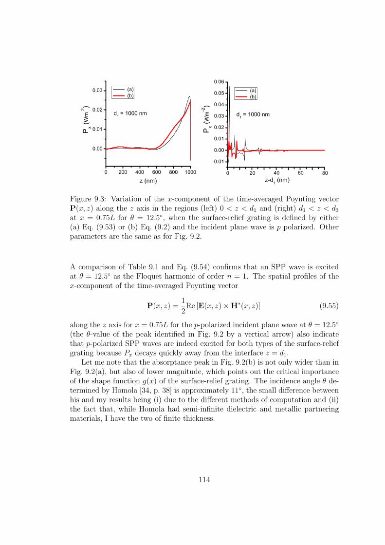
0 200 400 600 800 1000
0.00
0.01
0.02
0.03
-0.01
0.00
0.01
0.02
0.03
0.04
0.05
0.06P
x (Wm
-2)
d1 = 1000 nm
z (nm)
(a) (b)
0 20 40 60 80
Px (W
m-2)
d1 = 1000 nm
z-d1 (nm)
(a) (b)
Figure 9.3: Variation of the x-component of the time-averaged Poynting vectorP(x, z) along the z axis in the regions (left) 0 < z < d1 and (right) d1 < z < d3at x = 0.75L for θ = 12.5, when the surface-relief grating is defined by either(a) Eq. (9.53) or (b) Eq. (9.2) and the incident plane wave is p polarized. Otherparameters are the same as for Fig. 9.2.
A comparison of Table 9.1 and Eq. (9.54) confirms that an SPP wave is excitedat θ = 12.5 as the Floquet harmonic of order n = 1. The spatial profiles of thex-component of the time-averaged Poynting vector
P(x, z) =1
2Re [E(x, z)×H∗(x, z)] (9.55)
along the z axis for x = 0.75L for the p-polarized incident plane wave at θ = 12.5
(the θ-value of the peak identified in Fig. 9.2 by a vertical arrow) also indicatethat p-polarized SPP waves are indeed excited for both types of the surface-reliefgrating because Px decays quickly away from the interface z = d1.
Let me note that the absorptance peak in Fig. 9.2(b) is not only wider than inFig. 9.2(a), but also of lower magnitude, which points out the critical importanceof the shape function g(x) of the surface-relief grating. The incidence angle θ de-termined by Homola [34, p. 38] is approximately 11, the small difference betweenhis and my results being (i) due to the different methods of computation and (ii)the fact that, while Homola had semi-infinite dielectric and metallic partneringmaterials, I have the two of finite thickness.
114

9.3.2 Periodically nonhomogeneous dielectric partneringmaterial
Now let me move on to the excitation of multiple SPP waves by a surface-reliefgrating where the dielectric partnering material has a periodic nonhomogeneitynormal to the mean metal/dielectric interface:
ϵd(z) =
[(nb + na
2
)+
(nb − na
2
)sin
(πd2 − z
Ω
)]2, z > 0 , (9.56)
where 2Ω is the period. I chose na = 1.45 and nb = 2.32, the same parameters aswere used in Ch. 3. For all calculations reported in the remainder of this paper,I chose the metal to be bulk aluminum (ϵm = −56 + 21i) and the free-spacewavelength λ0 = 633 nm. The surface-relief grating is defined by Eq. (9.2) withL1 = 0.5L. I fixed Nt = 8 after ascertaining that the absorptances for Nt = 8converged to within ±1% of the absorptances calculated with Nt = 9. The gratingdepth d2− d1 = 50 nm and the thickness d3− d2 = 30 nm were also fixed, as theirvariations would not qualitatively affect the excitation of multiple SPP waves.Numerical results for Ω = λ0 and Ω = 1.5λ0 are now presented.
Ω = λ0
Let me commence with Ω = λ0. The solution of the corresponding canonicalboundary-value problem (when both the rugate filter and the metal are semi-infinite in thickness and their interface is planar) results in five p-polarized and twos-polarized SPP waves, the relative wavenmbers κ/k0 being provided in Table 9.2.I used the solution of the canonical boundary-value problem as a guide to choosethe grating period L and as a reference for the relative wavenumbers of SPPwaves. To analyze the excitation of s-polarized SPP waves in the grating-coupledconfiguration, I calculated the absorptance
As = 1−n=Nt∑n=−Nt
(∣∣r(n)s
∣∣2 + ∣∣t(n)s
∣∣2)Re(k(n)z
k(0)z
)(9.57)
for a(n)s = δn0 V m−1 and a
(n)p ≡ 0 ∀n ∈ Z. Both Ap and As were calculated as
functions of θ for d1 ∈ 4Ω, 5Ω, 6Ω, with Ng and Nd selected to have slices ofthickness 2 nm in the region 0 ≤ z ≤ d1 but 1 nm in the region d1 < z < d2. TheMathematicaTM program to calculate Ap versus θ is provided in Appendix B.6.The code for As is the same except that the matrix [P ] is different for s-polarizedincidence.
For all three values of d1, a peak is present at θ = 37.7 in the plots of Ap vs. θ
in Fig. 9.4(a). The relative wavenumbers k(n)x /k0 of several Floquet harmonics at
this incidence angle are given in Table 9.3. At θ = 37.7, k(1)x /k0 = 1.6115 is close
115

Table 9.2: Relative wavenumbers κ/k0 of possible SPP waves obtained by thesolution of the canonical boundary-value problem (Ch. 3) for Ω = λ0. Otherparameters are provided in the beginning of Sec. 9.3.2. If κ represents an SPPwave propagating in the ux direction, −κ represents an SPP wave propagating inthe −ux direction.
s-pol 1.48639 + 0.00132i 1.7324 + 0.0014i 1.9836 + 0.0006i∗
2.2128 + 9.6× 10⁻⁵i∗
p-pol 1.36479 + 0.00169i 1.61782 + 0.00548i 1.87437 + 0.00998i2.06995 + 0.01526i 2.21456 + 0.00246i
∗These solutions were missed in: M. Faryad and A. Lakhtakia, “Grating-coupledexcitation of multiple surface-plasmon-polariton waves,” Phys. Rev. A 84,033852 (2011).
15 20 25 30 35 40
0.2
0.4
0.6
0.8
10 15 20 25 30 350.0
0.2
0.4
0.6
0.8
1.0
A p
(b)
A s
(deg)
(a)
Figure 9.4: Absorptances (a) Ap and (b) As as functions of the incidence angle θ,when the surface-relief grating is defined by Eq. (9.2) with L1 = 0.5L, λ0 = 633 nm,Ω = λ0, and L = λ0. Black squares are for d1 = 6Ω, red circles for d1 = 5Ω, andblue triangles for d1 = 4Ω. The grating depth (d2−d1 = 50 nm) and the thicknessof the metallic layer (d3 − d2 = 30 nm) are the same for all plots. Each verticalarrow identifies an SPP wave.
116
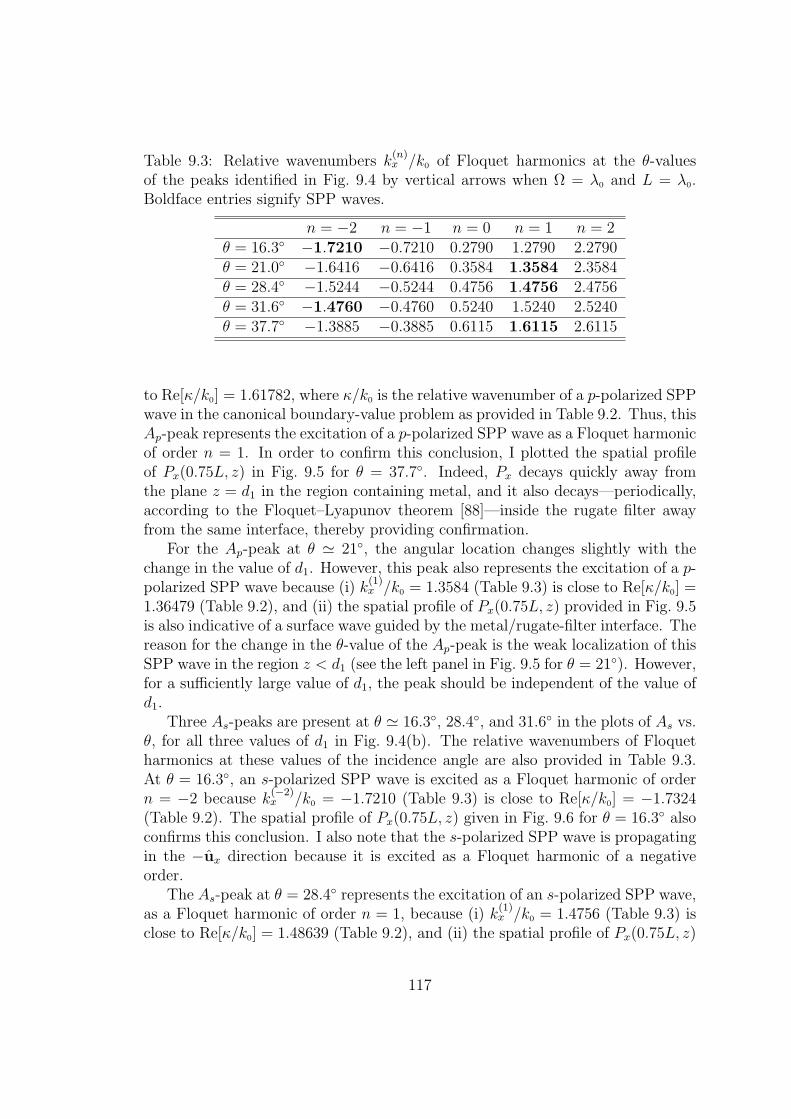
Table 9.3: Relative wavenumbers k(n)x /k0 of Floquet harmonics at the θ-values
of the peaks identified in Fig. 9.4 by vertical arrows when Ω = λ0 and L = λ0.Boldface entries signify SPP waves.
n = −2 n = −1 n = 0 n = 1 n = 2θ = 16.3 −1.7210 −0.7210 0.2790 1.2790 2.2790θ = 21.0 −1.6416 −0.6416 0.3584 1.3584 2.3584θ = 28.4 −1.5244 −0.5244 0.4756 1.4756 2.4756θ = 31.6 −1.4760 −0.4760 0.5240 1.5240 2.5240θ = 37.7 −1.3885 −0.3885 0.6115 1.6115 2.6115
to Re[κ/k0] = 1.61782, where κ/k0 is the relative wavenumber of a p-polarized SPPwave in the canonical boundary-value problem as provided in Table 9.2. Thus, thisAp-peak represents the excitation of a p-polarized SPP wave as a Floquet harmonicof order n = 1. In order to confirm this conclusion, I plotted the spatial profileof Px(0.75L, z) in Fig. 9.5 for θ = 37.7. Indeed, Px decays quickly away fromthe plane z = d1 in the region containing metal, and it also decays—periodically,according to the Floquet–Lyapunov theorem [88]—inside the rugate filter awayfrom the same interface, thereby providing confirmation.
For the Ap-peak at θ ≃ 21, the angular location changes slightly with thechange in the value of d1. However, this peak also represents the excitation of a p-polarized SPP wave because (i) k
(1)x /k0 = 1.3584 (Table 9.3) is close to Re[κ/k0] =
1.36479 (Table 9.2), and (ii) the spatial profile of Px(0.75L, z) provided in Fig. 9.5is also indicative of a surface wave guided by the metal/rugate-filter interface. Thereason for the change in the θ-value of the Ap-peak is the weak localization of thisSPP wave in the region z < d1 (see the left panel in Fig. 9.5 for θ = 21). However,for a sufficiently large value of d1, the peak should be independent of the value ofd1.
Three As-peaks are present at θ ≃ 16.3, 28.4, and 31.6 in the plots of As vs.θ, for all three values of d1 in Fig. 9.4(b). The relative wavenumbers of Floquetharmonics at these values of the incidence angle are also provided in Table 9.3.At θ = 16.3, an s-polarized SPP wave is excited as a Floquet harmonic of ordern = −2 because k
(−2)x /k0 = −1.7210 (Table 9.3) is close to Re[κ/k0] = −1.7324
(Table 9.2). The spatial profile of Px(0.75L, z) given in Fig. 9.6 for θ = 16.3 alsoconfirms this conclusion. I also note that the s-polarized SPP wave is propagatingin the −ux direction because it is excited as a Floquet harmonic of a negativeorder.
The As-peak at θ = 28.4 represents the excitation of an s-polarized SPP wave,as a Floquet harmonic of order n = 1, because (i) k
(1)x /k0 = 1.4756 (Table 9.3) is
close to Re[κ/k0] = 1.48639 (Table 9.2), and (ii) the spatial profile of Px(0.75L, z)
117
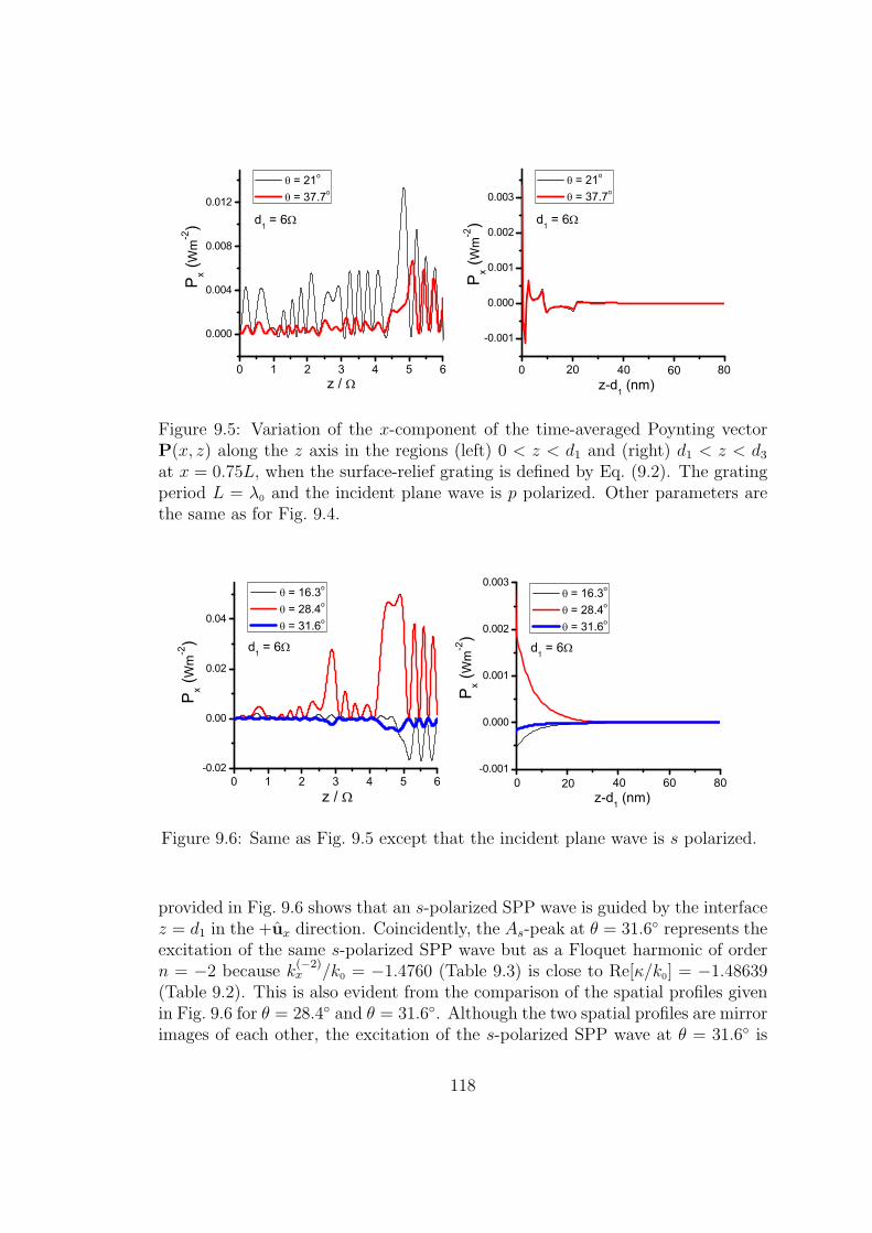
0 1 2 3 4 5 6
0.000
0.004
0.008
0.012
-0.001
0.000
0.001
0.002
0.003P
x (Wm
-2) d1 = 6
z /
= 21o
= 37.7o
Px (W
m-2)
z-d1 (nm)
d1 = 6
= 21o
= 37.7o
0 20 40 60 80
Figure 9.5: Variation of the x-component of the time-averaged Poynting vectorP(x, z) along the z axis in the regions (left) 0 < z < d1 and (right) d1 < z < d3at x = 0.75L, when the surface-relief grating is defined by Eq. (9.2). The gratingperiod L = λ0 and the incident plane wave is p polarized. Other parameters arethe same as for Fig. 9.4.
0 1 2 3 4 5 6-0.02
0.00
0.02
0.04
-0.001
0.000
0.001
0.002
0.003
Px (W
m-2) d1 = 6
z /
= 16.3o
= 28.4o
= 31.6o
Px (W
m-2)
z-d1 (nm)
d1 = 6
= 16.3o
= 28.4o
= 31.6o
0 20 40 60 80
Figure 9.6: Same as Fig. 9.5 except that the incident plane wave is s polarized.
provided in Fig. 9.6 shows that an s-polarized SPP wave is guided by the interfacez = d1 in the +ux direction. Coincidently, the As-peak at θ = 31.6 represents theexcitation of the same s-polarized SPP wave but as a Floquet harmonic of ordern = −2 because k
(−2)x /k0 = −1.4760 (Table 9.3) is close to Re[κ/k0] = −1.48639
(Table 9.2). This is also evident from the comparison of the spatial profiles givenin Fig. 9.6 for θ = 28.4 and θ = 31.6. Although the two spatial profiles are mirrorimages of each other, the excitation of the s-polarized SPP wave at θ = 31.6 is
118

not very efficient because it is excited as a Floquet harmonic of a higher order(|n| = 2).
25 30 35 40 45 50 55 60 65 70
0.2
0.4
0.6
0.8
20 25 30 35 40 45 50 55 60 65 700.0
0.2
0.4
0.6
0.8
1.0
(a)A s
A p
(deg)
(b)
Figure 9.7: Same as Fig. 9.4 except for L = 0.75λ0.
Table 9.4: Relative wavenumbers k(n)x /k0 of Floquet harmonics at the θ-values of
the peaks identified in Fig. 9.7 by vertical arrows when Ω = λ0 and L = 0.75λ0.Boldface entries signify SPP waves.
n = −2 n = −1 n = 0 n = 1 n = 2θ = 22.8 −2.2792 −0.9458 0.3875 1.7208 3.0542θ = 32.5 −2.1294 −0.7960 0.5373 1.8760 3.2040θ = 40.1 −2.0225 −0.6892 0.6441 1.9775 3.3108θ = 50.9 −1.8906 −0.5573 0.7760 2.1094 3.4427θ = 61.4 −1.7887 −0.4553 0.8780 2.2113 3.5446θ = 64.2 −1.7664 −0.4330 0.9003 2.2336 3.5670
Since not all possible SPP waves (predicted from the solution of the canonicalboundary-value problem) can be excited with period L = λ0 of the surface-reliefgrating, the grating period needs to be changed in order to excite the remainingSPP waves. The plots of Ap and As vs. θ for L = 0.75λ0 are presented in
119
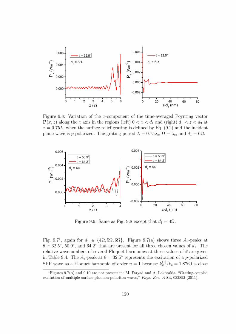
0 1 2 3 4 5 6
0.000
0.002
0.004
0.006
-0.002
0.000
0.002
0.004
0.006P
x (Wm
-2)
Px ( W
m-2)
z /
d1 = 6
= 32.5o
z-d1 (nm)
d1 = 6
= 32.5o
0 20 40 60 80
Figure 9.8: Variation of the x-component of the time-averaged Poynting vectorP(x, z) along the z axis in the regions (left) 0 < z < d1 and (right) d1 < z < d3 atx = 0.75L, when the surface-relief grating is defined by Eq. (9.2) and the incidentplane wave is p polarized. The grating period L = 0.75λ0, Ω = λ0, and d1 = 6Ω.
0 1 2 3 4
0.000
0.002
0.004
0.006
-0.002
0.000
0.002
0.004
Px (W
m-2) d1 = 4
= 50.9o
= 64.2o
Px (W
m-2)
z / z-d1 (nm)
d1 = 4
= 50.9o
= 64.2o
0 20 40 60 80
Figure 9.9: Same as Fig. 9.8 except that d1 = 4Ω.
Fig. 9.71, again for d1 ∈ 4Ω, 5Ω, 6Ω. Figure 9.7(a) shows three Ap-peaks atθ ≃ 32.5, 50.9, and 64.2 that are present for all three chosen values of d1. Therelative wavenumbers of several Floquet harmonics at these values of θ are givenin Table 9.4. The Ap-peak at θ = 32.5 represents the excitation of a p-polarized
SPP wave as a Floquet harmonic of order n = 1 because k(1)x /k0 = 1.8760 is close
1Figures 9.7(b) and 9.10 are not present in: M. Faryad and A. Lakhtakia, “Grating-coupledexcitation of multiple surface-plasmon-polariton waves,” Phys. Rev. A 84, 033852 (2011).
120

0 1 2 3 4 5 6-0.020.000.020.040.060.080.100.120.140.160.180.200.220.24
0.000
0.001
0.002
0.003 = 22.8o
= 40.1o
= 61.4o
d1 = 6
Px (W
m-2)
z /
= 22.8o
= 40.1o
= 61.4o
d1 = 6
Px (W
m-2)
z-d1 (nm)0 20 40 60 80
Figure 9.10: Same as Fig. 9.6 except for L = 0.75λ0.
to Re (1.87437 + 0.00998i) in Table 9.2. The spatial profile of Px(0.75L, z) givenin Fig. 9.8 also supports this conclusion. Similarly, the Ap-peaks at θ = 50.9 and64.2 represent the excitation of two other p-polarized SPP waves as a Floquetharmonic of the same order (n = 1), as is evident from the comparison of Tables 9.3and 9.4, and from the spatial profiles of Px(0.75L, z) provided in Fig. 9.9.
In the plots of As vs. θ in Fig. 9.7(b), three peaks at θ ≃ 22.8, 40.1, and 61.4
are present independent of the value of d1. The relative wavenumbers of severalFloquet harmonics at these values of θ are also given in Table 9.4. All of theseAs-peaks represent the excitation of s-polarized SPP waves as Floquet harmonicsof order n = 1 as can be seen by the comparison of Tables 9.3 and 9.4, and fromthe spatial profiles of Px(0.75L, z) provided in Fig. 9.10. It may be noted that thesame s-polarized SPP wave is excited as a Floquet harmonic of order n = 1 atθ = 22.8 in Fig. 9.7(b) and as a Floquet harmonic of order n = −1 in Fig. 9.4(b)at θ = 16.3.
Ω = 1.5λ0
The relative wavenumbers of possible SPP waves that can be guided by the pla-nar interface of the chosen rugate filter and the metal are given in Table 9.5 forΩ = 1.5λ0. In this case, the solution of the canonical boundary-value problemindicated that four s-polarized and six p-polarized SPP waves can be guided bythe metal/rugate-filter interface. For computations, the region d1 < z < d2 wasagain divided into 1-nm-thick slices; however, the region 0 ≤ z ≤ d1 was dividedinto 3-nm-thick slices to reduce the computation time, after ascertaining that theaccuracy of the computed reflectances and transmittances had not been adverselyaffected.
In the plots of Ap vs. θ for L = 0.8λ0, provided in Fig. 9.11, the excitation of
121

Table 9.5: Same as Table 9.2 except for Ω = 1.5λ0.
s-pol 1.4363 + 0.00025i 1.61507 + 0.00114i 1.78735 + 0.00078i1.9512 + 0.00037i
p-pol 1.40725 + 0.00052i 1.54121 + 0.00374i 1.71484 + 0.0049i1.88541 + 0.00739i 2.11513 + 0.0045i 2.02159 + 0.01301i
5 10 15 20 25 30 35 40 45 50 55
0.2
0.4
0.6
0.8
1.0
A p
(deg)
Figure 9.11: Absorptance Ap as a function of the incidence angle θ, when thesurface-relief grating is defined by Eq. (9.2) with L1 = 0.5L, λ0 = 633 nm, Ω =1.5λ0, and L = 0.8λ0. Black squares are for d1 = 6Ω, red circles for d1 = 5Ω, andblue triangles for d1 = 4Ω. The grating depth (d2 − d1 = 50 nm) and the width ofthe metallic layer (d3 − d2 = 30 nm) are the same for all the plots. Each verticalarrow indicates an SPP wave.
Table 9.6: Relative wavenumbers k(n)x /k0 of Floquet harmonics at the θ-values of
the peaks identified in Fig. 9.11 by vertical arrows when Ω = 1.5λ0 and L = 0.8λ0.Boldface entries signify SPP waves.
n = −2 n = −1 n = 0 n = 1 n = 2θ = 8.8 −2.3470 −1.0970 0.1530 1.4030 2.6530θ = 16.3 −2.2193 −0.9693 0.2807 1.5307 2.7807θ = 20.8 −2.1416 −0.8916 0.3584 1.6084 2.8584θ = 27.5 −2.0382 −0.7882 0.4618 1.7118 2.9618θ = 37.3 −1.8940 −0.6440 0.6060 1.8560 3.1060θ = 40 −1.8572 −0.6072 0.6428 1.8928 3.1428θ = 51.8 −1.7141 −0.4641 0.7859 2.0359 3.2859
p-polarized SPP waves is indicated at seven values of the incidence angle: θ ≃ 8.8,16.3, 20.8, 27.5, 37.3, 40, and 51.8. The relative wavenumbers k
(n)x /k0 of a few
122

Floquet harmonics at these values of the incidence angle are given in Table 9.6.The Ap-peak at θ = 8.8 represents the excitation of a p-polarized SPP wave
because k(1)x /k0 = 1.4030 is close to Re [κ/k0] = 1.40725 (Table 9.5). The spatial
profile of Px(0.75L, z) given in Fig. 9.12 for θ = 8.8 confirms the excitation of a p-polarized SPP wave; however, the SPP wave is very loosely bound to the interfacez = d1 in the region 0 < z < d1.
0 1 2 3 4 5 6
0.00
0.01
0.02
0.03
-0.002
0.000
0.002
0.004
Px (W
m-2)
z /
d1 = 6
= 8.8o
Px (W
m-2)
z-d1 (nm)
d1 = 6
= 8.8o
0 20 40 60 80
Figure 9.12: Variation of the x-component of the time-averaged Poynting vectorP(x, z) along the z axis in the regions (left) 0 < z < d1 and (right) d1 < z < d3 atx = 0.75L, when the surface-relief grating is defined by Eq. (9.2) and the incidentplane wave is p polarized. The grating period L = 0.8λ0 and d1 = 6Ω.
The Ap-peak at θ = 16.3 represents the excitation of another p-polarized SPP
wave, because k(1)x /k0 = 1.5307 is close to Re [κ/k0] = 1.54121 (Table 9.5). The
Ap-peak at θ = 20.8 also represents a p-polarized SPP wave because k(−2)x /k0 =
−2.1416 is close to Re [κ/k0] = −2.11513 (Table 9.5). Similarly, the Ap-peak atθ = 27.5 is due to the excitation of another p-polarized SPP wave as a Floquetharmonic of order n = 1. The spatial profiles of Px(0.75L, z) given in Fig. 9.13(a)for three different p-polarized plane waves incident at θ = 16.3, 20.8, and 27.5
also confirm that SPP waves are excited as Floquet harmonic of order n = 1,n = −2, and n = 1, respectively.
A comparison of Tables 9.5 and 9.6 shows that the Ap-peaks at θ = 37.3 and40 represent the excitation of the same p-polarized SPP wave; however, the SPPwave is excited as a Floquet harmonic of order n = −2 at θ = 37.3 but of ordern = 1 at θ = 40. Similarly, a p-polarized SPP wave is excited as a Floquetharmonic of order n = 1 at θ = 51.8. The spatial profiles of Px(0.75L, z) given inFig. 9.13(b) also support these conclusions.
In the plots of As vs. θ for L = 0.6λ0, provided in Fig. 9.14, four peaks at
123

0 1 2 3 4
-0.005
0.000
0.005
0.010
0.015
0.020
-0.006
-0.003
0.000
0.003
Px (W
m-2)
d1 = 4
= 16.3o
= 20.8o
= 27.5o
Px (W
m-2)
z /
d1 = 4 = 16.3o
= 20.8o
= 27.5o
0 20 40 60 80z-d1 (nm)
(a)
0 1 2 3 4
-0.003
0.000
0.003
0.006
0.009
-0.003
0.000
0.003
0.006
Px (W
m-2)
d1 = 4
= 37.3o
= 40o
= 51.8o
(b)
Px (W
m-2)
z /
d1 = 4
= 37.3o
= 40o
= 51.8o
0 20 40 60 80z-d1 (nm)
Figure 9.13: Same as Fig. 9.12 except that d1 = 4Ω.
0 5 10 15 200.0
0.2
0.4
0.6
0.8
1.0
(deg)
A s
Figure 9.14: Same as Fig. 9.11 except that As is plotted instead of Ap, and L =0.6λ0.
124

Table 9.7: Relative wavenumbers k(n)x /k0 of Floquet harmonics at the θ-values of
the peaks identified in Fig. 9.14 by vertical arrows when Ω = 1.5λ0 and L = 0.6λ0.Boldface entries signify SPP waves.
n = −2 n = −1 n = 0 n = 1 n = 2θ = 3.7 −3.2688 −1.6021 0.0645 1.7312 3.3979θ = 6.4 −3.2219 −1.5552 0.1115 1.7781 3.4448θ = 13.5 −3.0999 −1.4332 0.2334 1.9001 3.5668θ = 16.2 −3.0543 −1.3877 0.2790 1.9457 3.6123
0 1 2 3 4
-0.10
-0.05
0.00
0.05
0.10
0.15
-0.004
-0.002
0.000
0.002
0.004
Px (W
m-2)
d1 = 4
= 3.7o
= 6.4o
Px (W
m-2)
z /
d1 = 4
= 3.7o
= 6.4o
0 20 40 60 80z-d1 (nm)
Figure 9.15: Variation of the x-component of the time-averaged Poynting vectorP(x, z) along the z axis in the regions (left) 0 < z < d1 and (right) d1 < z < d3 atx = 0.75L for two s-polarized incident plane waves, when the surface-relief gratingis defined by Eq. (9.2). The grating period L = 0.6λ0, d1 = 4Ω, and Ω = 1.5λ0.
θ ≃ 3.7, 6.4, 13.5, and 16.2 are present for all values of d1. The As-peakat θ = 3.7 represents the excitation of an s-polarized SPP wave as a Floquetharmonic of order n = −1 because k
(1)x /k0 = −1.6021 is close to Re [κ/k0] =
−1.61507 (Table 9.5), which is a solution of the canonical boundary-value problemfor an s-polarized SPP wave, whereas the As-peak at θ = 6.4 represents theexcitation of another s-polarized SPP wave because k
(1)x /k0 = 1.7781 is close to
Re [κ/k0] = 1.78735 (Table 9.5). Similarly, two s-polarized SPP waves are excitedas a Floquet harmonic of order n = 1 at θ = 13.5 and of order n = −1 atθ = 16.2, respectively, as is evident from the comparison of Tables 9.6 and 9.7.The spatial profiles of Px(0.75L, z) given in Figs. 9.15 and 9.16 confirm theseconclusions.
125

0 1 2 3 4 5 6
-0.05
0.00
0.05
0.10
0.15
-0.004
-0.002
0.000
0.002
0.004
d1 = 6
= 13.5o
= 16.2o
Px (W
m-2)
z /
Px (W
m-2) d1 = 6
= 13.5o
= 16.2o
0 20 40 60 80z-d1 (nm)
Figure 9.16: Same as Fig. 9.15 except that d1 = 6Ω.
9.4 Concluding Remarks
In the last two subsections, I have deciphered a host of numerical results andidentified those absorptance peaks that indicate the excitation of SPP waves inthe grating-coupled configuration, when the dielectric partnering material is peri-odically nonhomogeneous normal to the mean plane of the surface-relief grating.It was found that
(i) the periodic nonhomogeneity of the dielectric partnering material enablesthe excitation of multiple SPP waves of both p- and s-polarization states;
(ii) fewer s-polarized SPP waves are excited than p-polarized SPP waves;
(iii) for a given period of the surface-relief grating, it is possible for two planewaves with different angles of incidence to excite the same SPP wave (Figs. 9.4(b) and 9.11);
(iv) not all SPP waves predicted by the solution of the canonical problem maybe excited in the grating-coupled configuration for a given period of thesurface-relief grating;
(v) the absorptance peaks representing the excitation of p-polarized SPP wavesare generally wider than those representing s-polarized SPP waves;
(vi) the absorptance peak is narrower for an SPP wave of higher phase speed(i.e. smaller Re(κ)); and
(vii) an SPP wave that is excited as a Floquet harmonic of order n = +1 forθ ∈ [0, π/2)—or n = −1 for θ ∈ (−π/2, 0], by virtue of symmetry—is themost efficient (Fig. 9.6).
126

It may be noted that some other combination of the periodic functions ϵd(z) andg(x) may allow all solutions of the canonical boundary-value problem to be excitedin the grating-coupled configuration with a specific d1, d2, d3.
127

Chapter 10
Enhanced Absorption of LightDue to Multiple SPP Waves‡
10.1 Introduction
For the last three decades, research to bring down the cost of photovoltaic (PV)solar cells has gained a huge momentum and many techniques to increase theefficiency of light harvesting by solar cells have been investigated. Among othermethods [121], the use of plasmonic structures to enhance the absorption of lightby PV solar cells has been studied [3,122,123]. The basic idea is to have periodictexturing of the metallic backing layer of a thin-film solar cell to help excite surface-plasmon-polariton (SPP) waves. As the partnering semiconductor in these studieshas been homogeneous, only one SPP wave (of p-polarization state) at a givenfrequency can be excited [13, 16] leading to modest gains in the absorption oflight.
In the last chapters, it has been shown that multiple SPP waves of differentpolarization states, phase speeds, and attenuation rates can be guided by the inter-face of a metal and a dielectric material that is periodically nonhomogeneous in thedirection normal to the metallic/dielectric interface. Also, it was shown in Ch. 9that multiple SPP waves can be excited using a grating-coupled configuration.Therefore, I set out to investigate if light absorption can be enhanced due to theexcitation of multiple SPP waves by a surface-relief grating on the metallic back-ing layer in a PV solar cell with a periodically nonhomogeneous semiconductor.For this purpose, a boundary-value problem of reflection by a surface-relief gratingcoated with a periodically nonhomogeneous semiconductor was investigated. Thetheoretical formulation of the boundary-value problem using the rigorous coupled-wave approach (RCWA) is explained in Ch. 9, and is not repeated in this chapter.Numerical results are presented and discussed in Sec. 10.2, and concluding remarks
‡This chapter is based on: M. Faryad and A. Lakhtakia, “Enhanced absorption of light duemultiple surface-plasmon-polariton waves,” Proc. SPIE 8110, 81100F (2011).
128

are presented in Sec. 10.3.
10.2 Numerical Results and Discussion
The absorptance
Ap = 1−n=Nt∑n=−Nt
(∣∣r(n)p
∣∣2 + ∣∣t(n)p
∣∣2)Re(k(n)z
k(0)z
)(10.1)
for a p-polarized incident plane wave (a(n)p = δn0 and a
(n)s ≡ 0 ∀n ∈ Z) and the
absorptance
As = 1−n=Nt∑n=−Nt
(∣∣r(n)s
∣∣2 + ∣∣t(n)s
∣∣2)Re(k(n)z
k(0)z
), (10.2)
for an s-polarized incident plane wave (a(n)s = δn0 and a
(n)p ≡ 0∀n ∈ Z) were
calculated as functions of the incidence angle θ. The value of Nd was chosen so asto have 2 nm-thick slices in the region 0 < z < d1, and fixed Nt = 8 and Ng = 50after ascertaining that the absorptances converged. I also fixed d3 − d2 = 30 nmand set
ϵd(z) = ϵr
[1 + γ sin
(πd2 − z
Ω
)]2, (10.3)
where 2Ω is the period and γ ∈ [0, 1]. Numerical results for homogeneous and peri-odically nonhomogeneous semiconductor partnering materials are now presented.
10.2.1 Homogeneous semiconductor partnering material
Suppose that the semiconductor is homogeneous: γ = 0. For illustrative purposes,I chose this material to be a-Si1−xCx : H with ϵr = 11 + 0.01i [124, Fig. 1(c)] atλ0 = 620 nm, and the metal as bulk aluminum: ϵm = −56 + 21i [125]. Theinterface of the chosen homogeneous semiconductor and metal can guide only onep-polarized SPP wave with the relative wavenumber
κ/k0 =√ϵrϵm/(ϵr + ϵm) = 3.6368 + 0.1436i (10.4)
but no s-polarized SPP waves [13,16].The absorptances Ap and As vs. θ are given in Fig. 10.1 for two values of
d1 with a surface-relief grating of period L = 186 nm, and for one value of d1without a surface-relief grating (i.e., Lg = 0). The absorptances were calculatedfor two values of d1 in order to distinguish between [70] (i) waveguide modes thatdepend on the thickness of the semiconductor layer [104] and (ii) surface wavesthat should be independent of that thickness when the semiconductor layer is suffi-ciently thick. In Fig. 10.1(a), a peak at θ ≃ 17 is present regardless of the value of
129
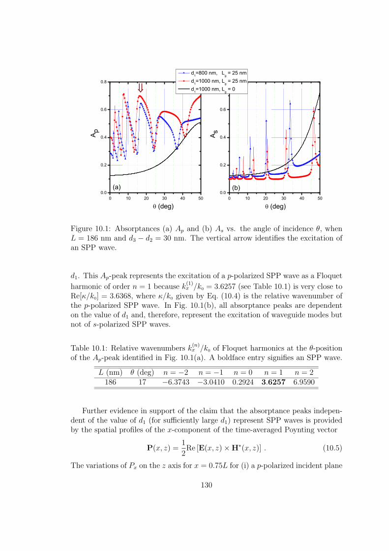
0 10 20 30 40 500.0
0.2
0.4
0.6
0.8
0 10 20 30 40 500.0
0.2
0.4
0.6
0.8
(b)(a)
d1=800 nm, L
g = 25 nm
d1=1000 nm, L
g = 25 nm
d1=1000 nm, L
g = 0
(deg) (deg)
A sA p
Figure 10.1: Absorptances (a) Ap and (b) As vs. the angle of incidence θ, whenL = 186 nm and d3 − d2 = 30 nm. The vertical arrow identifies the excitation ofan SPP wave.
d1. This Ap-peak represents the excitation of a p-polarized SPP wave as a Floquet
harmonic of order n = 1 because k(1)x /k0 = 3.6257 (see Table 10.1) is very close to
Re[κ/k0] = 3.6368, where κ/k0 given by Eq. (10.4) is the relative wavenumber ofthe p-polarized SPP wave. In Fig. 10.1(b), all absorptance peaks are dependenton the value of d1 and, therefore, represent the excitation of waveguide modes butnot of s-polarized SPP waves.
Table 10.1: Relative wavenumbers k(n)x /k0 of Floquet harmonics at the θ-position
of the Ap-peak identified in Fig. 10.1(a). A boldface entry signifies an SPP wave.
L (nm) θ (deg) n = −2 n = −1 n = 0 n = 1 n = 2186 17 −6.3743 −3.0410 0.2924 3.6257 6.9590
Further evidence in support of the claim that the absorptance peaks indepen-dent of the value of d1 (for sufficiently large d1) represent SPP waves is providedby the spatial profiles of the x-component of the time-averaged Poynting vector
P(x, z) =1
2Re [E(x, z)×H∗(x, z)] . (10.5)
The variations of Px on the z axis for x = 0.75L for (i) a p-polarized incident plane
130

-0.002
0.000
0.002
0.004
-0.012
-0.008
-0.004
0.000
0.004
0.008d1 = 800 nmd2 = d1+25 nmd3 = d2+30 nm
d3d3d2d2 d1
d1 00
Px
(b)(a)
z
d1 = 1000 nmd2 = d1+25 nmd3 = d2+30 nm
Px
z
Figure 10.2: Variation of the x-component of the time-averaged Poynting vectorPx along the z axis at x = 0.75L for (a) a p-polarized incident plane wave whenθ = 17, and (b) an s-polarized incident plane wave when θ = 13.3. The period ofthe surface-relief grating L = 186 nm and the free-space wavelength λ0 = 620 nm.All other parameters are the same as for Fig. 10.1. The horizontal scale for z ∈(d1, d3) is exaggerated with respect to that for z ∈ (0, d1).
wave at θ = 17 (the θ-value of the peak identified in Fig 10.1(a) by an arrow) and(ii) an s-polarized incident plane wave at θ = 13.3 (the θ-value of a randomlychosen peak in Fig. 10.1(b) for d1 = 1000 nm) are shown in Figs. 10.2(a) and(b), respectively. In Fig. 10.2(a), the energy is tightly bound to the plane z = d1suggesting that an SPP wave is excited as was claimed in the foregoing paragraph.However, Fig. 10.2(b) shows that the wave is being guided by the homogeneoussemiconductor layer, indicating a waveguide mode.
Figure 10.1 shows that the absorptance in the presence of a surface-relief grat-ing is generally higher than the absorptance without a surface-relief grating for p-polarized incident plane waves, while the difference is not significant for s-polarizedincident plane waves. Since both SPP waves and waveguide modes are excited byp-polarized incident plane waves, while only waveguide modes can be excited bys-polaarized incident plane waves, it can be inferred that the excitation of an SPPwave enhances the absorption.
10.2.2 Periodically nonhomogeneous semiconductor part-nering material
Let me now introduce periodic nonhomogeneity (γ = 0) in the semiconductorpartnering material normal to the mean interface of the surface-relief grating.The solution of the relevant canonical boundary-value problem (Ch. 3) shows that
131

the planar interface of a metal and a periodically nonhomogeneous semiconductorcan guide multiple SPP waves of both p- and s-polarization states. The resultsfor Ω = 200 nm and 300 nm are now presented and discussed.
Ω = 200 nm
Suppose that Ω = 200 nm, γ = 0.1, λ0 = 620 nm, ϵr = 11 + 0.01i [124, Fig. 1(c)],and ϵm = −56 + 21i [125]. The relative wavenumbers of SPP waves that can beguided by the planar interface of the metal and the chosen periodically nonhomo-geneous semiconductor were obtained by the solution of the canonical boundary-value problem and are given in Table 10.2. This table shows that two p- and ones-polarized SPP waves can be guided by the planar interface of the two chosenpartnering materials.
Table 10.2: Relative wavenumbers κ/k0 of p-polarized and s-polarized SPP wavessupported by the planar interface of bulk aluminum and the semiconductor char-acterized by Eq. (10.3), when Ω = 200 nm, γ = 0.1, and λ0 = 620 nm.
pol. state κ/k0
p 3.2276 + 0.0239i 3.8114 + 0.1390is 3.3889 + 0.0039i
Plots of the absorptances Ap and As vs. θ are provided in Fig. 10.3 for Lg = 0and Lg > 0. Two Ap-peaks, at θ ≃ 12 and 25.1, in Fig. 10.3(a) are independentof the thickness of the semiconductor layer. The relative wavenumbers of Floquetharmonics at these values of θ are given in Table 10.3. Since k
(1)x /k0 = 3.8550 at
θ = 12 is close to Re[κ/k0] = 3.8114 (Table 10.2), the first Ap-peak representsthe excitation of a p-polarized SPP wave as a Floquet harmonic of order n = 1.Similarly, the Ap-peak at θ = 25.1 in Fig. 10.3(a) represents the excitation ofanother p-polarized SPP wave as a Floquet harmonic of order n = −1. Thespatial profiles of the x-component of the time-averaged Poynting vector for thesetwo p-polarized SPP waves, provided in Fig. 10.4(a), support the conclusion thatp-polarized SPP waves are excited. Let me note that the p-polarized SPP wavethat is excited as a Floquet harmonic of order n = 1 propagates in the +ux
direction while the SPP wave that is excited as a Floquet harmonic of ordern = −1 propagates in the −ux propagation.
One As-peak at θ ≃ 16.2 is present in Fig. 10.3(b) independent of the valueof d1 when Lg = 0. The relative wavenumbers of Floquet harmonics at this valueof θ are also given in Table 10.3. A comparison of Tables 10.2 and 10.3 showsthat an s-polarized SPP wave is excited as a Floquet harmonic of order n = 1 atθ = 16.2. The variation of Px along the z axis given in Fig. 10.4(b) also indicatesthe excitation of an s-polarized SPP wave.
132

0 10 20 30 400.0
0.2
0.4
0.6
0.8
0 10 20 30 400.0
0.2
0.4
0.6
0.8
1.0
(b)
A p
(deg)
d1=7 , L
g = 20 nm
d1=8 , L
g = 20 nm
d1=8 , L
g = 0
(a)
d1=8 , L
g = 0
d1=8 , L
g = 25 nm
d1=7 , L
g = 25 nm
(deg) A
s
Figure 10.3: Absorptances (a) Ap and (b) As vs. the angle of incidence θ, whenΩ = 200 nm, γ = 0.1, d3 − d2 = 30 nm, and λ0 = 620 nm. Also, (a) L = 170 nm,and (b) L = 200 nm. Each vertical arrow indicates the excitation of an SPP wave.
Table 10.3: Relative wavenumbers k(n)x /k0 of Floquet harmonics at the θ-values of
the absorptance peaks in Fig. 10.3. Boldface entries signify SPP waves.
L (nm) θ (deg) n = −2 n = −1 n = 0 n = 1 n = 2170 12 −7.0862 −3.4392 0.2079 3.8550 7.5020170 25.1 −6.8699 −3.2229 0.4242 4.0713 7.7183200 16.2 −5.9210 −2.8210 0.2790 3.3790 6.4790
The excitation of two p-polarized SPP waves is accompanied by a very signifi-cant increase in the absorptance for a p-polarized incident plane wave, as is evidentfrom the comparison of the absorptances for Lg = 0 and Lg > 0 in Fig. 10.3(a).Similarly, the excitation of an s-polarized SPP wave in the grating-coupled config-uration is correlated with a significant increase in the absorptance in Fig. 10.3(b).
Ω = 300 nm
Let me now present the numerical results for Ω = 300 nm and γ = 0.1. Thesolution of the canonical boundary-value problem shows that three p- and two s-polarized SPP waves—withe relative wavenumbers given in Table 10.4—are guided
133

-0.004
-0.002
0.000
0.002
0.004
0.006
-0.02
0.00
0.02
0.04
0.06
0.08
0.10
(b)
Px
d1 = 8d2 = d1+20 nmd3 = d2+30 nm
z
= 12o
= 25.1o
(a)
0 0d3 d3d2d2 d1
d1
Px
d1 = 8d2 = d1+25 nmd3 = d2+30 nm
z
= 16.2o
Figure 10.4: Variation of the x-component of the time-averaged Poynting vectorPx along the z axis at x = 0.75L for (a) two p-polarized incident plane waves and(b) an s-polarized incident plane wave, at the θ-values of the absorptance peaksidentified in Fig. 10.3 by vertical arrows. The horizontal scale for z ∈ (d1, d3) isexaggerated with respect to that for z ∈ (0, d1).
by the planar interface of the chosen metal and the periodically nonhomogeneoussemiconductor at λ0 = 620 nm.
Table 10.4: Same as Table 10.2 except for Ω = 300 nm.
pol. state κ/k0
p 3.0552 + 0.0097i 3.4109 + 0.0187i 3.7688 + 0.1327is 3.1453 + 0.0038i 3.4856 + 0.0024i
The absorptances Ap and As as functions of θ are given in Fig. 10.5 for Lg =0 and Lg > 0. In Fig. 10.5(a), three peaks at θ ≃ 7.7, 13.4, and 39.4 areindependent of the value of d1 when Lg > 0. The relative wavenumbers of Floquetharmonics at these values of θ are provided in Table 10.5, and a comparison ofTables 10.4 and 10.5 shows that each Ap-peak represents the excitation of a p-polarized SPP wave. The spatial profiles of Px along the z axis at x = 0.75L givenin Fig. 10.6(a) also suggests the same conclusion.
Two peaks are present in Fig. 10.5(b) at θ ≃ 10.3 and 31.8, independentof the value of d1 in the absorptance curves for the grating-coupled configuration(i.e., Lg > 0). The relative wavenumbers of Floquet harmonics at these values ofθ are also given in Table 10.5. A comparison of Tables 10.4 and 10.5 shows thatan s-polarized SPP wave is excited corresponding to each As-peak as a Floquet
134

0 10 20 30 40 500.0
0.2
0.4
0.6
0.8
1.0
0 10 20 30 40 500.0
0.2
0.4
0.6
0.8
1.0
(b)(a)
A sA p
(deg)
d1=8 , L
g = 20 nm
d1=7 , L
g = 20 nm
d1=8 , L
g = 0
d1=8 , L
g = 25 nm
d1=7 , L
g = 25 nm
d1=8 , L
g = 0
(deg)
Figure 10.5: Same as Fig. 10.3 except for Ω = 300 nm, and (a) L = 195 nm and(b) L = 210 nm.
Table 10.5: Relative wavenumbers k(n)x /k0 of Floquet harmonics at the θ-values of
the absorptance peaks in Fig. 10.5. Boldface entries signify SPP waves.
L (nm) θ (deg) n = −2 n = −1 n = 0 n = 1 n = 2195 7.7 −6.2250 −3.0455 0.1339 3.3135 6.4930195 13.4 −6.1272 −2.9477 0.2318 3.4112 6.5907195 39.4 −5.7242 −2.5448 0.6347 3.8142 6.9937210 10.3 −5.7260 −2.7739 0.1788 3.1312 6.0837210 31.8 −5.3778 −2.4254 0.5270 3.4793 6.4317
harmonic of order n = 1. The spatial profiles of Px(x = 0.75L, z), given inFig. 10.6(b), at the θ-values of the As-peaks also show that s-polarized SPP wavesare indeed excited.
A comparison of plots for Lg = 0 and Lg > 0 in Fig. 10.5(a) for p-polarizedincident plane waves shows that the absorptance increases wherever an SPP wave isexcited, but this conclusion appears unwarranted from Fig. 10.5(b) for s-polarizedincident plane waves. However, the possibility of increasing As by changing thegrating period L still remains and requires further exploration.
The periodically nonhomogeneous semiconductor with Ω = 300 nm and γ = 0.1was also investigated at λ0 = 827 nm. The relative permittivity of a-Si1−xCx : H at
135

-0.006
-0.004
-0.002
0.000
0.002
0.004
0.006
0.00
0.01
0.02
0.03
0.04d1 = 8d2 = d1+20 nmd3 = d2+30 nm
Px
z
= 7.7o
= 13.4o
= 39.4o
(b)(a)
d1 = 8d2 = d1+25 nmd3 = d2+30 nm
Px
00 d3d3d2d2 d1
d1z
= 10.3o
= 31.8o
Figure 10.6: Variation of the x-component of the time-averaged Poynting vectorPx along the z axis at x = 0.75L for (a) three p-polarized incident plane waves and(b) two s-polarized incident plane waves, at the θ-values of the absorptance peaksidentified in Fig. 10.5 by vertical arrows. The horizontal scale for z ∈ (d1, d3) isexaggerated with respect to that for z ∈ (0, d1).
λ0 = 827 nm was taken to be ϵr = 10+0.005i [124, Fig. 1(c)] and of bulk aluminumas ϵm = −61.5+45.5i [125]. The solution of the canonical boundary-value problemfor these parameters shows that two p- and two s-polarized SPP waves can beguided by the planar interface of the metal and the periodically nonhomogeneoussemiconductor, with relative wavenumbers available in Table 10.6.
Table 10.6: Same as Table 10.4 except for λ0 = 827 nm, ϵr = 10 + 0.005i, andϵm = −61.5 + 45.5i.
pol. state κ/k0
p 3.0901 + 0.0378i 3.5004 + 0.1320is 2.7980 + 0.0052i 3.2485 + 0.0038i
For λ0 = 827 nm, the absorptances Ap and As are plotted as functions of θin Fig. 10.7, for Lg = 0 and Lg > 0. Two Ap-peaks at θ ≃ 2.6 and 16.4 inFig. 10.7(a), along with two As-peaks at θ ≃ 8.2 and 18.1 in Fig. 10.7(b), areindependent of the value of d1. The relative wavenumbers of Floquet harmonics atthe θ-values of these peaks are given in Table 10.7. Comparison of Tables 10.6 and10.7 show that each Ap- (As-) peak represents the excitation of a p- (s-) polarizedSPP wave. Moreover, Fig. 10.7 shows that, for both linear polarization states ofthe incident plane wave, the excitation of multiple SPP waves is accompanied bya significant enhancement of absorption.
136

0 10 20 30 40 500.0
0.2
0.4
0.6
0.8
1.0
0 10 20 30 40 500.0
0.2
0.4
0.6
0.8
1.0
(deg)A sA p
d1=7 , L
g = 20 nm
d1=8 , L
g = 20 nm
d1=8 , L
g = 0
d1=7 , L
g = 20 nm
d1=8 , L
g = 20 nm
d1=8 , L
g = 0
(b)(a)
(deg)
Figure 10.7: Same as Fig. 10.5 except for λ0 = 827 nm, ϵr = 10 + 0.005i, ϵm =−61.5 + 45.5i, and (a) L = 244.5 nm and (b) L = 282 nm.
Table 10.7: Relative wavenumbers k(n)x /k0 of Floquet harmonics at the θ-values of
the absorptance peaks in Fig. 10.7. Boldface entries signify SPP waves.
L (nm) θ (deg) n = −2 n = −1 n = 0 n = 1 n = 2244.5 2.6 −6.7195 −3.3371 0.0454 3.4278 6.8102244.5 16.4 −6.4825 −3.1001 0.2823 3.6648 7.0472282 8.2 −5.7226 −2.7900 0.1426 3.0752 6.0079282 18.1 −5.5546 −2.6220 0.3107 3.2433 6.1759
10.3 Concluding Remarks
The absorptances for p- and s-polarized incident plane waves were calculated asfunctions of the incidence angle θ, using RCWA, for a finitely thick and periodicallynonhomogeneous semiconductor layer on top of a metallic surface-relief grating.The excitation of surface plasmon-polariton waves was inferred from
(i) the absorptance peaks whose θ-locations were independent of the thicknessof the semiconductor layer when that layer was made sufficiently thick, andwas confirmed by the
(ii) analysis of the spatial profiles of the time-averaged Poynting vector.
137

Moreover, it was seen that
(iii) the use of a metallic surface-relief grating, as opposed to that of a metallicslab with planar faces, can significantly enhance absorption for both p- ands-polarized incidence when one or more SPP waves are excited.
138
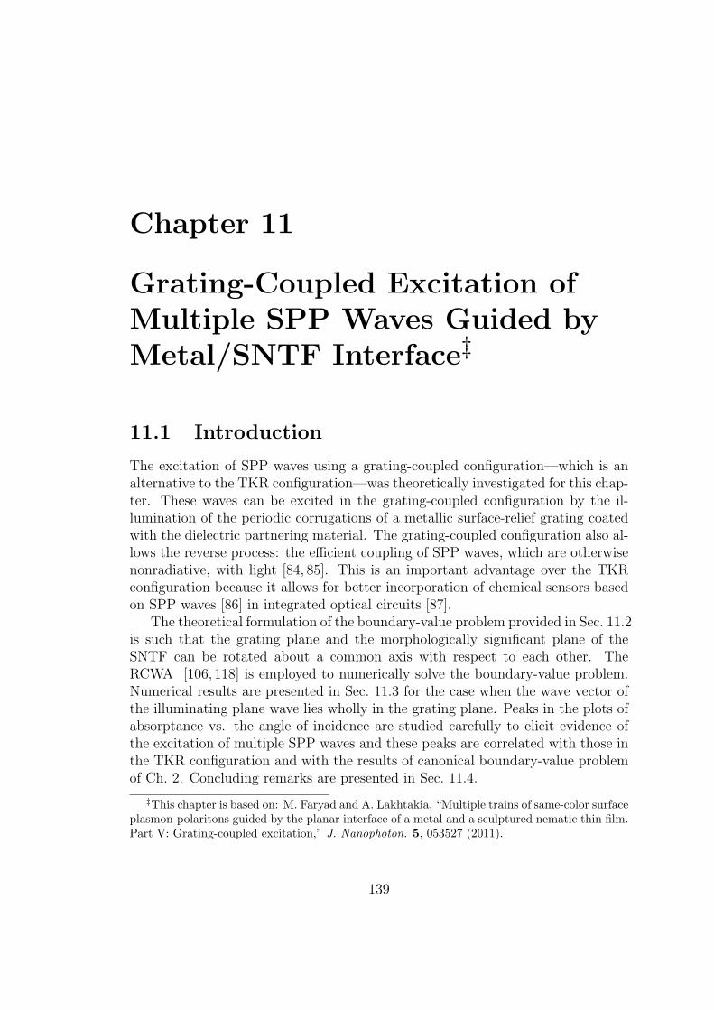
Chapter 11
Grating-Coupled Excitation ofMultiple SPP Waves Guided byMetal/SNTF Interface‡
11.1 Introduction
The excitation of SPP waves using a grating-coupled configuration—which is analternative to the TKR configuration—was theoretically investigated for this chap-ter. These waves can be excited in the grating-coupled configuration by the il-lumination of the periodic corrugations of a metallic surface-relief grating coatedwith the dielectric partnering material. The grating-coupled configuration also al-lows the reverse process: the efficient coupling of SPP waves, which are otherwisenonradiative, with light [84, 85]. This is an important advantage over the TKRconfiguration because it allows for better incorporation of chemical sensors basedon SPP waves [86] in integrated optical circuits [87].
The theoretical formulation of the boundary-value problem provided in Sec. 11.2is such that the grating plane and the morphologically significant plane of theSNTF can be rotated about a common axis with respect to each other. TheRCWA [106, 118] is employed to numerically solve the boundary-value problem.Numerical results are presented in Sec. 11.3 for the case when the wave vector ofthe illuminating plane wave lies wholly in the grating plane. Peaks in the plots ofabsorptance vs. the angle of incidence are studied carefully to elicit evidence ofthe excitation of multiple SPP waves and these peaks are correlated with those inthe TKR configuration and with the results of canonical boundary-value problemof Ch. 2. Concluding remarks are presented in Sec. 11.4.
‡This chapter is based on: M. Faryad and A. Lakhtakia, “Multiple trains of same-color surfaceplasmon-polaritons guided by the planar interface of a metal and a sculptured nematic thin film.Part V: Grating-coupled excitation,” J. Nanophoton. 5, 053527 (2011).
139

11.2 Boundary-Value Problem
11.2.1 Description
Let me consider the boundary-value problem shown schematically in Fig. 11.1.The regions z < 0 and z > d3 are vacuous. The region 0 ≤ z ≤ d1 is occupied byan SNTF with a periodically nonhomogeneous permittivity dyadic [44,70,71]
ϵSNTF
(z) = ϵ0 Sz(γ−) · S
y(z) · ϵ
ref(z) · S−1
y(z) · S−1
z(γ−) , (11.1)
where the dyadics
Sy(z) = (uxux + uzuz) cos [χ(z)] + (uzux − uxuz) sin [χ(z)] + uyuy
ϵref
(z) = ϵa(z) uzuz + ϵb(z) uxux + ϵc(z) uyuy
(11.2)
depend on the vapor incidence angle χv(z) = χv + δv sin [π(d2 − z)/Ω] that issupposedly made to vary sinusoidally with period 2Ω during the deposition of theSNTF by a physical evaporation process in a vacuum chamber. The third dyadicin Eq. (11.1) was chosen as
Sz(γ−) = (uxux + uyuy) cos γ
− + (uyux − uxuy) sin γ− + uzuz , (11.3)
so that the plane formed by the unit vectors uz and ux cos γ− + uy sin γ
− is themorphologically significant plane of the SNTF. Thus, there is sufficient flexibilityin the formulation with respect to the orientation of the morphologically significantplane. The region d2 ≤ z ≤ d3 is occupied by the partnering metallic materialwith spatially uniform relative permittivity ϵm.
The region d1 < z < d2 contains a metallic surface-relief grating of periodL along the x axis, with the SNTF present in the troughs. The xz plane is thegrating plane. The relative permittivity dyadic ϵ
g(x, z) = ϵ
g(x±L, z) in this region
is taken to be as
ϵg(x, z) =
ϵmI −
[ϵmI + ϵ
SNTF(z)]U [d2 − z − g(x)] , x ∈ (0, L1) ,
ϵSNTF
(z) , x ∈ (L1, L) ,(11.4)
for z ∈ (d1, d2), withI = uxux + uyuy + uzuz , (11.5)
g(x) = (d2 − d1) sin (πx/L1) , L1 ∈ (0, L) , (11.6)
and
U(ζ) =
1 , ζ ≥ 0 ,
0 , ζ < 0 .(11.7)
The depth of the surface-relief grating defined by Eq. (11.6) is Lg = d2−d1. Let menote that the permittivity dyadic defined by Eq. (11.4) is a simplistic description
140
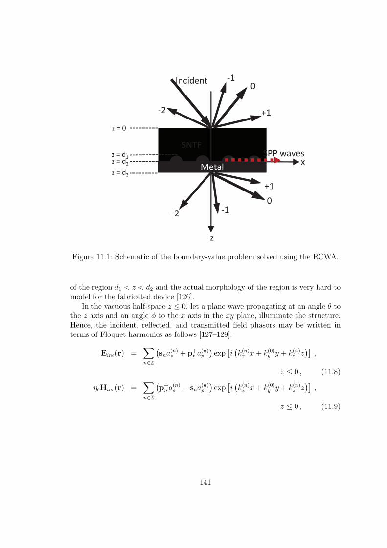
SPP waves
SNTF
Metal
Incident
z
x
z = 0
z = d1
z = d2
z = d3
Metal
0
+1
-1
-2
0
+1
-1 -2
Figure 11.1: Schematic of the boundary-value problem solved using the RCWA.
of the region d1 < z < d2 and the actual morphology of the region is very hard tomodel for the fabricated device [126].
In the vacuous half-space z ≤ 0, let a plane wave propagating at an angle θ tothe z axis and an angle ϕ to the x axis in the xy plane, illuminate the structure.Hence, the incident, reflected, and transmitted field phasors may be written interms of Floquet harmonics as follows [127–129]:
Einc(r) =∑n∈Z
(sna
(n)s + p+
n a(n)p
)exp
[i(k(n)x x+ k(0)y y + k(n)z z
)],
z ≤ 0 , (11.8)
η0Hinc(r) =∑n∈Z
(p+n a
(n)s − sna
(n)p
)exp
[i(k(n)x x+ k(0)y y + k(n)z z
)],
z ≤ 0 , (11.9)
141

Eref (r) =∑n∈Z
(snr
(n)s + p−
n r(n)p
)exp
[i(k(n)x x+ k(0)y y − k(n)z z
)],
z ≤ 0 , (11.10)
η0Href (r) =∑n∈Z
(p−n r
(n)s − snr
(n)p
)exp
[i(k(n)x x+ k(0)y y − k(n)z z
)],
z ≤ 0 , (11.11)
Etr(r) =∑n∈Z
(snt
(n)s + p+
n t(n)p
)exp
i[k(n)x x+ k(0)y y + k(n)z (z − d3)
],
z ≥ d3 , (11.12)
η0Htr(r) =∑n∈Z
(p+n t
(n)s − snt
(n)p
)exp
i[k(n)x x+ k(0)y y + k(n)z (z − d3)
],
z ≥ d3 , (11.13)
where k(n)x = k0 cosϕ sin θ + nκx, κx = 2π/L, k
(0)y = k0 sinϕ sin θ,
k(n)xy =
√(k
(n)x )
2+ (k
(0)y )
2, (11.14)
and
k(n)z =
+
√k20 − (k
(n)xy )
2, k20 > (k
(n)xy )
2
+i
√(k
(n)xy )
2− k20 , k20 < (k
(n)xy )
2. (11.15)
The unit vectors
sn =−k(0)y ux + k
(n)x uy
k(n)xy
(11.16)
and
p±n = ∓k
(n)z
k0
(k(n)x ux + k
(0)y uy
k(n)xy
)+k(n)xy
k0
uz (11.17)
represent the s- and p-polarization states, respectively. Whereasa(n)s , a
(s)p
,
n ∈ Z, are the known amplitudes of the incident electric field phasor, the reflection
amplitudesr(n)s , r
(s)p
and the transmission amplitudes
t(n)s , t
(s)p
, n ∈ Z, have
to be determined.
11.2.2 Coupled ordinary differential equations
The relative permittivity dyadic in the region 0 ≤ z ≤ d3 can be expanded as aFourier series with respect to x, viz.,
ϵ(x, z) =∑n∈Z
ϵ(n)(z) exp(inκxx) , z ∈ [0, d3] , (11.18)
142

where
ϵ(0)(z) =
ϵSNTF
(z) , z ∈ [0, d1] ,
1L
∫ L
0ϵg(x, z)dx , z ∈ (d1, d2) ,
ϵmI , z ∈ [d2, d3] ,
(11.19)
and
ϵ(n)(z) =
1L
∫ L
0ϵg(x, z) exp(−inκxx)dx , z ∈ [d1, d2]
0 , otherwise;∀n = 0 , (11.20)
where 0 is the null dyadic. The coefficient dyadic ϵ(n)(z) on the right side ofEq. (11.18) can be expanded as
ϵ(n)(z) = ϵ(n)xx (z)uxux + ϵ(n)xy (z)uxuy + ϵ(n)xz (z)uxuz
+ ϵ(n)yx (z)uyux + ϵ(n)yy (z)uyuy + ϵ(n)yz (z)uyuz
+ ϵ(n)zx (z)uzux + ϵ(n)zy (z)uzuy + ϵ(n)zz (z)uzuz . (11.21)
The field phasors may be written in the region 0 ≤ z ≤ d3 in terms of Floquetharmonics as
E(r) =∑n∈Z
[E(n)
x (z)ux + E(n)y (z)uy + E(n)
z (z)uz
]exp
[i(k(n)x x+ k(0)y y
)]H(r) =
∑n∈Z
[H(n)
x (z)ux +H(n)y (z)uy +H(n)
z (z)uz
]exp
[i(k(n)x x+ k(0)y y
)] ,
z ∈ [0, d3] , (11.22)
with unknown functions E(n)x,y,z(z) and H
(n)x,y,z(z). Substitution of Eqs. (11.18) and
(11.22) in the frequency-domain Maxwell curl postulates results in a system offour ordinary differential equations
d
dzE(n)
x (z)− ik(n)x E(n)z (z) = ik0η0H
(n)y (z) , (11.23)
d
dzE(n)
y (z)− ik(0)y E(n)z (z) = −ik0η0H
(n)x (z) , (11.24)
d
dzH(n)
x (z)− ik(n)x H(n)z (z) = − ik0
η0
×∑m∈Z
[ϵ(n−m)yx (z)E(m)
x (z) + ϵ(n−m)yy (z)E(m)
y (z) + ϵ(n−m)yz (z)E(m)
z (z)],
(11.25)
d
dzH(n)
y (z)− ik(0)y H(n)z (z) =
ik0
η0
×∑m∈Z
[ϵ(n−m)xx (z)E(m)
x (z) + ϵ(n−m)xy (z)E(m)
y (z) + ϵ(n−m)xz (z)E(m)
z (z)],
(11.26)
143

and two algebraic equations
k(n)x E(n)y (z)− k(0)y E(n)
x (z) = k0η0H(n)z (z) , (11.27)
k(n)x H(n)y (z)− k(0)y H(n)
x (z) = −k0
η0
×∑m∈Z
[ϵ(n−m)zx (z)E(m)
x (z) + ϵ(n−m)zy (z)E(m)
y (z) + ϵ(n−m)zz (z)E(m)
z (z)].
(11.28)
Equations (11.23)–(11.28) hold ∀z ∈ (0, d3) and ∀n ∈ Z. These equations canbe recast into an infinite system of coupled first-order ordinary differential equa-tions, but that system can not be implemented on a digital computer. Therefore,I restrict |n| ≤ Nt and then define the column (2Nt + 1)-vectors
[Xσ(z)] = [X(−Nt)σ (z), X(−Nt)
σ (z), ..., X(0)σ (z), ..., X(Nt−1)
σ (z), X(Nt)σ (z)]T ,
(11.29)for X ∈ E,H and σ ∈ x, y, z. Similarly, I define (2Nt+1)×(2Nt+1)-matrixes
[Kx] = diag[k(n)x ] , [ϵ
αβ(z)] =
[ϵ(n−m)αβ (z)
], (11.30)
where diag[k(n)x ] is a diagonal matrix, α ∈ x, y, z, and β ∈ x, y, z.
Substitution of Eqs. (11.27) and (11.28) into Eqs. (11.23)–(11.26), to eliminate
E(n)z and H
(n)z ∀n ∈ Z, gives the matrix ordinary differential equation
d
dz
[f(z)
]= i[P (z)
]·[f(z)
], z ∈ (0, d3) , (11.31)
where the column vector [f(z)] with 4(2Nt + 1) components is defined as[f(z)
]=[[Ex(z)]
T , [Ey(z)]T , η0 [Hx(z)]
T , η0 [Hy(z)]T]T
; (11.32)
and the 4(2Nt + 1)× 4(2Nt + 1)-matrix[P (z)
]is given by
[P (z)
]=
[P
11(z)] [
P12(z)] [
P13(z)] [
P14(z)]
[P
21(z)] [
P22(z)] [
P23(z)] [
P24(z)]
[P
31(z)] [
P32(z)] [
P33(z)] [
P34(z)]
[P
41(z)] [
P42(z)] [
P43(z)] [
P44(z)]
, (11.33)
144
where [P
11(z)]
= −[K
x
]·[ϵzz(z)]−1
·[ϵzx(z)], (11.34)[
P12(z)]
= −[K
x
]·[ϵzz(z)]−1
·[ϵzy(z)], (11.35)[
P13(z)]
=k(0)y
k0
[K
x
]·[ϵzz(z)]−1
, (11.36)[P
14(z)]
= k0
[I]− 1
k0
[K
x
]·[ϵzz(z)]−1
·[K
x
], (11.37)[
P21(z)]
= −k(0)y
[ϵzz(z)]−1
·[ϵzx(z)], (11.38)[
P22(z)]
= −k(0)y
[ϵzz(z)]−1
·[ϵzy(z)], (11.39)[
P23(z)]
= −k0
[I]+k(0)y
2
k0
[ϵzz(z)]−1
, (11.40)[P
24(z)]
= −k(0)y
k0
[ϵzz(z)]−1
·[K
x
], (11.41)
[P
31(z)]
= −k0
[ϵyx(z)]+ k0
[ϵyz(z)]·[ϵzz(z)]−1
·[ϵzx(z)]− k
(0)y
k0
[K
x
](11.42)[
P32(z)]
=1
k0
[K
x
]2− k0
[ϵyy(z)]+ k0
[ϵyz(z)]·[ϵzz(z)]−1
·[ϵzy(z)],
(11.43)[P
33(z)]
= −k(0)y
[ϵyz(z)]·[ϵzz(z)]−1
, (11.44)[P
34(z)]
=[ϵyz(z)]·[ϵzz(z)]−1
·[K
x
], (11.45)[
P41(z)]
= k0
[ϵxx(z)]− k0
[ϵxz(z)]·[ϵzz(z)]−1
·[ϵzx(z)]− k
(0)y
2
k0
[I],
(11.46)[P
42(z)]
= k0
[ϵxy(z)]− k0
[ϵxz(z)]·[ϵzz(z)]−1
·[ϵzy(z)]+k(0)y
k0
[K
x
],
(11.47)[P
43(z)]
= k(0)y
[ϵxz(z)]·[ϵzz(z)]−1
, (11.48)[P
44(z)]
= −[ϵxz(z)]·[ϵzz(z)]−1
·[K
x
], (11.49)
and[I]is the (2Nt + 1)× (2Nt + 1) identity matrix.
145

When ϕ = 0,[P
13(z)]=[P
21(z)]=[P
22(z)]=[P
24(z)]=[P
33(z)]=[P
43(z)]=[0],
(11.50)where
[0]is the (2Nt + 1)× (2Nt + 1) null matrix; and[
P12(z)]=[P
31(z)]=[P
34(z)]=[P
42(z)]=[0], (11.51)
andϵSNTF
(z) = ϵ0 Sy(z) · ϵ
ref(z) · S−1
y(z) (11.52)
when γ− = 0 as well. Thus, when γ− = ϕ = 0, k(0)y = 0,[
ϵxz(z)]=[ϵzx(z)], (11.53)[
ϵxy(z)]=[ϵyx(z)]=[ϵyz(z)]=[ϵzy(z)]=[0], (11.54)
and
[P (z)
]=
[P
11(z)] [
0] [
0)] [
P14(z)]
[0] [
0]
−k0
[I] [
0][
0] [
P32(z)] [
0] [
0][
P41(z)] [
0] [
0] [
P44(z)]
. (11.55)
11.2.3 Solution algorithm
The column vectors[f(0)
]and
[f(d3)
]can be written using Eqs. (11.8)–(11.13)
as
[f(0)
]=
[Y +
e
] [Y −
e
][Y +
h
] [Y −
h
] ·
[[A]
[R]
],
[f(d3)
]=
[Y +
e
][Y +
h
] · [T] , (11.56)
where
[A] =[a(−Nt)s , a(−Nt+1)
s , ..., a(0)s , ..., a(Nt−1)s , a(Nt)
s ,
a(−Nt)p , a(−Nt+1)
p , ..., a(0)p , ..., a(Nt−1)p , a(Nt)
p
]T, (11.57)
[R] =[r(−Nt)s , r(−Nt+1)
s , ..., r(0)s , ..., r(Nt−1)s , r(Nt)
s ,
r(−Nt)p , r(−Nt+1)
p , ..., r(0)p , ..., r(Nt−1)p , r(Nt)
p
]T, (11.58)
[T] =[t(−Nt)s , t(−Nt+1)
s , ..., t(0)s , ..., t(Nt−1)s , t(Nt)
s ,
t(−Nt)p , t(−Nt+1)
p , ..., t(0)p , ..., t(Nt−1)p , t(Nt)
p
]T, (11.59)
146

and the nonzero entries of (4Nt + 2)× (4Nt + 2)-matrixes[Y ±
e,h
]are as follows:
(Y ±h
)nm
=
sn · ux , n = m ∈ [1, 2Nt + 1] ,
p±n · uy , n = m ∈ [2Nt + 2, 4Nt + 2] ,
p±n · ux , n = m+ 2Nt + 1 ,
sn · uy , n = m− 2Nt + 1 ,
(11.60)
(Y ±e
)nm
=
p±n · ux , n = m ∈ [1, 2Nt + 1] ,
−sn · uy , n = m ∈ [2Nt + 2, 4Nt + 2] ,
−sn · ux , n = m+ 2Nt + 1 ,
p±n · uy , n = m− 2Nt + 1 .
(11.61)
In order to devise a stable algorithm to determine the unknown [R] and [T]for known [A] [106–109], the region 0 ≤ z ≤ d1 is divided into Nd slices and theregion d1 ≤ z ≤ d2 into Ng slices, but the region d2 ≤ z ≤ d3 is kept as just oneslice. So, there are Nd +Ng +1 slices and Nd +Ng +2 interfaces. In the jth slice,j ∈ [1, Nd +Ng + 1], bounded by the planes z = zj−1 and z = zj, I approximate[
P (z)]=[P]j=
[P
(zj + zj−1
2
)], z ∈ (zj, zj−1) , (11.62)
with z0 = 0 and zNd+Ng+1 = d3. Equation (11.31) yields [130][f(zj−1)
]=[G]j· exp
−i∆j
[D]j
·[G]−1
j·[f(zj)
], (11.63)
where ∆j = zj − zj−1,[G]jis a square matrix comprising the eigenvectors of
[P]j
as its columns, and the diagonal matrix[D]jcontains the eigenvalues of
[P]jin
the same order.Let me define auxiliary column vectors [T]j and auxiliary transmission matrixes[
Z]jby the relation [108][
f(zj)]=[Z]j· [T]j , j ∈ [0, Nd +Ng + 1] ; (11.64)
hence,
[T]Nd+Ng+1 = [T] , and[Z]Nd+Ng+1
=
[Y +
e
][Y +
h
] . (11.65)
To find [T]j and[Z]jfor j ∈ [0, Nd +Ng], I substitute Eq. (11.64) in (11.63),
which results in the relation[Z]j−1
· [T]j−1 =[G]j·[e−i∆j [D]uj 0
0 e−i∆j [D]lj
]·[G]−1
j·[Z]j· [T]j ,
j ∈ [1, Nd +Ng + 1] , (11.66)
147

where[D]ujand
[D]ljare the upper and lower diagonal submatrixes of
[D]j, re-
spectively, when the eigenvalues are arranged in decreasing order of the imaginarypart.
Since both [T]j and[Z]jcannot be determined simultaneously from Eq. (11.66),
let me formulate [108]
[T]j−1 = exp−i∆j
[D]uj
·[W]uj· [T]j , (11.67)
where the square matrix[W]ujand its counterpart
[W]ljare defined via[ [
W]uj[
W]lj
]=[G]−1
j·[Z]j. (11.68)
Substitution of Eq. (11.67) in (11.66) results in the relation
[Z]j−1
=[G]j·
[ [I]
exp−i∆j[D]lj
·[W]lj·[W]uj
−1
· expi∆j[D]uj
] ,j ∈ [1, Nd +Ng + 1] . (11.69)
From Eqs. (11.68) and (11.69), I find[Z]0in terms of
[Z]Nd+Ng+1
. After parti-
tioning [Z]0=
[ [Z]u0[
Z]l0
], (11.70)
and using Eqs. (11.56) and (11.64), [R] and [T]0 are found as follows:
[[T]0[R]
]=
[Z]u0 −[Y −
e
][Z]l0
−[Y −
h
] −1
·
[Y +
e
][Y +
h
] · [A] . (11.71)
Equation (11.71) was obtained by enforcing the usual boundary conditionsacross the plane z = 0. After [T]0 is known, [T] = [T]Nd+Ng+1 is found by
reversing the sense of iterations in Eq. (11.67).
11.2.4 Absorptance
For planewave illumination, a(n)s = a
(n)p = 0 ∀n ∈ [−Nt,−1]∪ [1, Nt]. The elements
of the 2× 2 matrixes in the relations[r(n)s
r(n)p
]=
[r(n)ss r
(n)sp
r(n)ps r
(n)pp
]·
[a(0)s
a(0)p
], n ∈ Z , (11.72)
148
and [t(n)s
t(n)p
]=
[t(n)ss t
(n)sp
t(n)ps t
(n)pp
]·
[a(0)s
a(0)p
], n ∈ Z , (11.73)
are the reflection and transmission coefficients. Co-polarized coefficients have bothsubscripts identical, but cross-polarized coefficients do not. Reflectances and trans-
mittances of order n are defined, for example, as R(n)sp = |r(n)sp |2Re
[k(n)z /k
(0)z
]and
T(n)sp = |t(n)sp |2Re
[k(n)z /k
(0)z
].
The planewave absorptance of the structure is given by
A = 1−Nt∑
n=−Nt
|r(n)s |2 + |r(n)p |2 + |t(n)s |2 + |t(n)p |2
|a(0)s |2 + |a(0)p |2Re
(k(n)z
k(0)z
). (11.74)
This expression can be written in terms of the reflection and transmission coeffi-cients as
A = As|a(0)s |2
|a(0)s |2 + |a(0)p |2+ Ap
|a(0)p |2
|a(0)s |2 + |a(0)p |2
+Nt∑
n=−Nt
(r(n)ss r
(n)sp
∗+ r(n)ps r
(n)pp
∗+ t(n)ss t
(n)sp
∗+ t(n)ps t
(n)pp
∗) a
(0)s a
(0)p
∗
|a(0)s |2 + |a(0)p |2Re
(k(n)z
k(0)z
)
+Nt∑
n=−Nt
(r(n)ss
∗r(n)sp + r(n)ps
∗r(n)pp + t(n)ss
∗t(n)sp + t(n)ps
∗t(n)pp
) a(0)s
∗a(0)p
|a(0)s |2 + |a(0)p |2Re
(k(n)z
k(0)z
),
(11.75)
whereAs = 1−
∑n∈Z
R(n)ss +R(n)
ps + T (n)ss + T (n)
ps (11.76)
is the absorptance for s-polarized illumination and
Ap = 1−∑n∈Z
R(n)sp +R(n)
pp + T (n)sp + T (n)
pp (11.77)
is the absorptance for p-polarized illumination.
11.3 Numerical Results and Discussion
For the illustrative numerical results presented in this section, I chose the sameparameters for the periodically nonhomogeneous SNTF and the metal as in Ch. 2.The free-space wavelength was fixed at λ0 = 633 nm, and the metal was taken
149
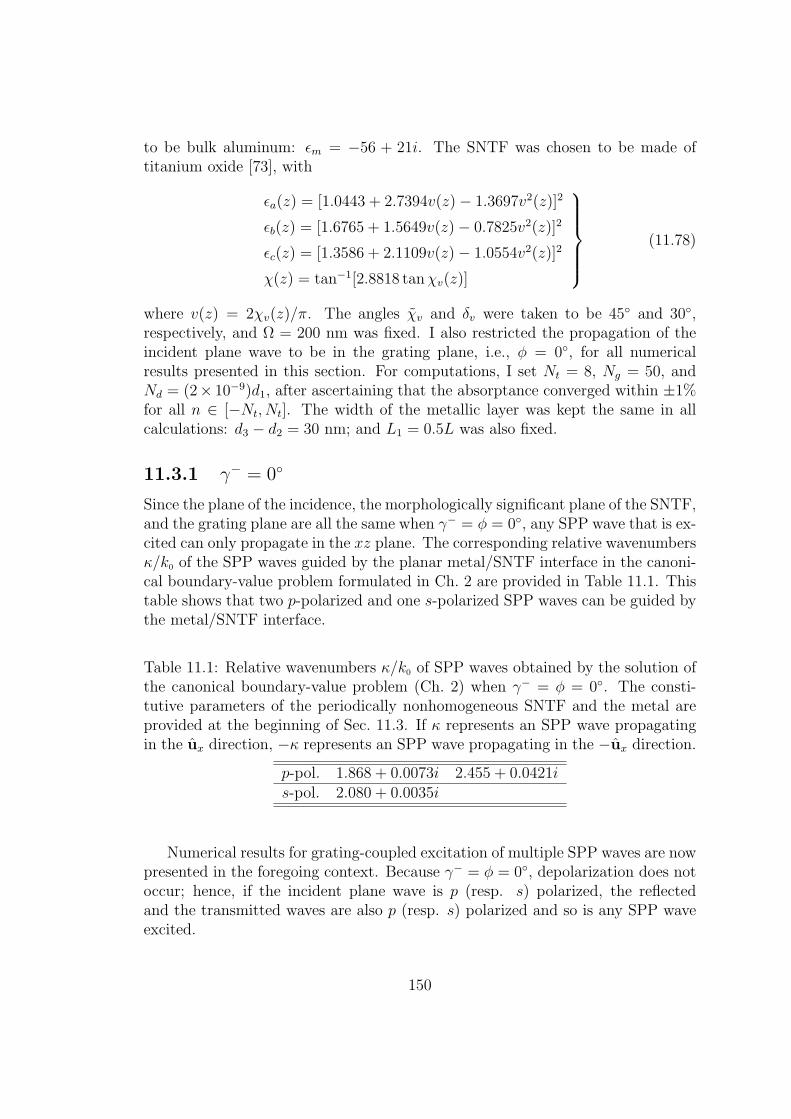
to be bulk aluminum: ϵm = −56 + 21i. The SNTF was chosen to be made oftitanium oxide [73], with
ϵa(z) = [1.0443 + 2.7394v(z)− 1.3697v2(z)]2
ϵb(z) = [1.6765 + 1.5649v(z)− 0.7825v2(z)]2
ϵc(z) = [1.3586 + 2.1109v(z)− 1.0554v2(z)]2
χ(z) = tan−1[2.8818 tanχv(z)]
(11.78)
where v(z) = 2χv(z)/π. The angles χv and δv were taken to be 45 and 30,respectively, and Ω = 200 nm was fixed. I also restricted the propagation of theincident plane wave to be in the grating plane, i.e., ϕ = 0, for all numericalresults presented in this section. For computations, I set Nt = 8, Ng = 50, andNd = (2× 10⁻⁹)d1, after ascertaining that the absorptance converged within ±1%for all n ∈ [−Nt, Nt]. The width of the metallic layer was kept the same in allcalculations: d3 − d2 = 30 nm; and L1 = 0.5L was also fixed.
11.3.1 γ− = 0
Since the plane of the incidence, the morphologically significant plane of the SNTF,and the grating plane are all the same when γ− = ϕ = 0, any SPP wave that is ex-cited can only propagate in the xz plane. The corresponding relative wavenumbersκ/k0 of the SPP waves guided by the planar metal/SNTF interface in the canoni-cal boundary-value problem formulated in Ch. 2 are provided in Table 11.1. Thistable shows that two p-polarized and one s-polarized SPP waves can be guided bythe metal/SNTF interface.
Table 11.1: Relative wavenumbers κ/k0 of SPP waves obtained by the solution ofthe canonical boundary-value problem (Ch. 2) when γ− = ϕ = 0. The consti-tutive parameters of the periodically nonhomogeneous SNTF and the metal areprovided at the beginning of Sec. 11.3. If κ represents an SPP wave propagatingin the ux direction, −κ represents an SPP wave propagating in the −ux direction.
p-pol. 1.868 + 0.0073i 2.455 + 0.0421is-pol. 2.080 + 0.0035i
Numerical results for grating-coupled excitation of multiple SPP waves are nowpresented in the foregoing context. Because γ− = ϕ = 0, depolarization does notoccur; hence, if the incident plane wave is p (resp. s) polarized, the reflectedand the transmitted waves are also p (resp. s) polarized and so is any SPP waveexcited.
150

Excitation by a p-polarized incident plane wave
9 10 11 12 13 140.2
0.4
0.6
0.8
1.0
(deg)
A p d
1 = 7 , L
g = 25nm
d1 = 7 , L
g = 20nm
d1 = 8 , L
g = 20nm
Figure 11.2: Absorptance Ap vs. the angle of incidence θ when L = 380 nm,ϕ = γ− = 0, and d3 − d2 = 30 nm. The absorptance peak represents theexcitation of a p-polarized SPP wave.
The absorptance Ap is plotted in Fig. 11.2 as a function of the angle of incidenceθ, when L = 380 nm and ϕ = γ− = 0, for three combinations of d1 and Lg. TheMathematicaTMcode is provided in Appendix B.7 to calculate Ap and As. Theabsorptance peak at θ ≃ 11.1 is present in Fig. 11.2 independent of thicknessd1 of the SNTF and the grating depth Lg. The presence of the peak for bothvalues of d1 indicates that this peak represents the excitation of a p-polarized SPPwave [70, 71]—and not of a waveguide mode [104, 105], which must depend ond1. The increase in the height of the Ap-peak with the increase in the value ofLg is another indicator that the peak represents the excitation of an SPP wavebecause the excitation efficiency is commonly held to increase with increasinggrating depth [34].
The relative wavenumbers k(n)x /k0 of a few Floquet harmonics at θ = 11.1
when L = 380 nm are presented in Table 11.2. A comparison of Tables 11.1and 11.2 shows that, as k
(1)x /k0 = 1.8583 is very close to Re (1.868 + 0.0073i), the
p-polarized SPP wave is excited as a Floquet harmonic of order n = 1.To examine the spatial variation of the power density of the SPP wave in the
151

Table 11.2: Relative wavenumbers k(n)x /k0 of Floquet harmonics at the θ-value of
the absorptance peak in Fig. 11.2 when L = 380 nm and ϕ = γ− = 0. A boldfaceentry signifies an SPP wave.
n = −2 n = −1 n = 0 n = 1 n = 2θ = 11.1 −3.1391 −1.4733 0.1925 1.8583 3.5241
structure, the time-averaged Poynting vector
P(x, z) =1
2Re [E(x, z)×H∗(x, z)] , (11.79)
was calculated. The x-component Px of P(x, z) is presented in Fig. 11.3 alongthe z axis when a p-polarized plane wave is incident on the structure at an angleθ = 11.1, L = 380 nm, and x = 0.25L or 0.75L. The spatial profiles show thatthe energy is bound to the plane z = d1 and most of the power density residesin the SNTF. This shows that a surface wave—a p-polarized SPP wave—is beingguided by the metal/SNTF interface. However, the SPP wave is weakly localizedto the plane z = d1 in the SNTF.
0 1 2 3 4 5 6 7 8-0.005
0.000
0.005
0.010
0.015
0.020
-0.005
0.000
0.005
0.010
0.015
0.020
Px (W
m-2)
z /
d1 = 8
d2 = d
1+20nm
d3 = d
2+30nm
x = 0.25 L x = 0.75 L
Px (W
m-2)
z-d1 (nm)
d1 = 8
d2 = d
1+20nm
d3 = d
2+30nm
x = 0.25 L x = 0.75 L
0 10 20 30 40 50
Figure 11.3: Variation of the x-component Px(x, z) of the time-averaged Poyntingvector P(x, z) along the z axis in the regions (left) 0 < z < d1 and (right) d1 < z <d3, when L = 380 nm and ϕ = γ− = 0. The incident plane wave is p polarizedand the angle of incidence θ = 11.1.
To excite the second p-polarized SPP wave predicted by the canonical boundary-value problem with κ/k0 = 2.455 + 0.0421i, the grating period L was reduced to280 nm. The absorptance Ap is presented as a function of θ in Fig. 11.4, when
152

6 9 12 15 18 210.1
0.2
0.3
0.4
0.5
0.6
A p
(deg)
d1 = 6 , L
g = 20nm
d1 = 6 , L
g = 25nm
d1 = 7 , L
g = 20nm
Figure 11.4: Same as Fig. 11.2 except that L = 280 nm.
L = 280 nm and γ− = ϕ = 0, again for three combinations of d1 and Lg. Anabsorptance peak at θ ≃ 13.6, which is present in all three curves, indicates theexcitation of a p-polarized SPP wave. The relative wavenumbers of a few Floquetharmonics at θ = 13.6 when L = 280 nm are provided in Table 11.3. Sincek(1)x /k0 = 2.4959 is very close to Re (2.455 + 0.0421i), the p-polarized SPP wave is
excited as a Floquet harmonic of order n = 1.
Table 11.3: Relative wavenumbers k(n)x /k0 of Floquet harmonics at the θ-value of
the absorptance peak in Fig. 11.4 when L = 280 nm. A boldface entry signifiesan SPP wave.
n = −2 n = −1 n = 0 n = 1 n = 2θ = 13.6 −4.2863 −2.0256 0.2351 2.4959 4.7566
The variations of Px(0.25L, z) and Px(0.75L, z) along the z axis are shown inFig. 11.5 when a p-polarized plane wave is incident on the structure at an angleθ = 13.6, and L = 280 nm. The plots show that the power density is stronglylocalized to the metal/SNTF interface. A comparison of Figs. 11.2 and 11.4 showthat the Ap-peak representing the excitation of a p-polarized SPP wave with asmaller phase speed—i.e., larger magnitude of Re(κ)—is broader. Also, the SPP
153

0 1 2 3 4 5 6 7-0.004
-0.002
0.000
0.002
0.004
0.006
0.008
-0.004
-0.002
0.000
0.002
0.004
0.006
0.008
z /
Px (W
m-2)
x = 0.25 L x = 0.75 L
d1 = 7
d2 = d
1+20nm
d3 = d
2+30nm
z-d1 (nm)
Px (W
m-2)
x = 0.25 L x = 0.75 L
d1 = 7
d2 = d
1+20nm
d3 = d
2+30nm
0 10 20 30 40 50
Figure 11.5: Same as Fig. 11.3 except that θ = 13.6 and L = 280 nm.
wave with the broader absorptance peak is more tightly localized in the SNTF tothe plane z = d1.
Excitation by an s-polarized incident plane wave
The absorptance As was calculated as a function of the angle of incidence θ whenL = 340 nm and γ− = ϕ = 0. In Fig. 11.6, As is presented with respect to θfor three combinations of d1 and Lg. The peaks present in the absorptance curvesfor d1 = 8Ω at θ ≃ 8.5 and 15, and for d1 = 7Ω at θ ≃ 12.1, are due tothe excitation of waveguide modes because their θ-positions are dependent on thevalue of d1.
An As-peak in Fig. 11.6 at θ ≃ 11.6 represents the excitation of an s-polarizedSPP wave because that peak exists for all values of d1. The change in the θ-positionof the peak when Lg is reduced from 25 to 20 nm is negligible. This absorptancepeak, representing the excitation of an s-polarized SPP wave, is narrower than ofthose representing the two p-polarized SPP waves in Sec. 11.3.1. Finally, I notethat the s-polarized SPP wave is also excited as a Floquet harmonic of order n = 1:k(1)x /k0 = 2.0628 in Table 11.4 is very close to Re (2.080 + 0.0035i) in Table 11.1.
Table 11.4: Relative wavenumbers k(n)x /k0 of Floquet harmonics at the θ-value of
the peak identified by a vertical arrow in Fig. 11.6 when L = 340 nm. A boldfaceentry signifies an SPP wave.
n = −2 n = −1 n = 0 n = 1 n = 2θ = 11.6 −3.5224 −1.6607 0.2011 2.0628 3.9246
154

8 10 12 14 160.0
0.2
0.4
0.6
0.8
1.0
A s
(deg)
d1 = 7 , L
g = 25nm
d1 = 8 , L
g = 20nm
d1 = 8 , L
g = 25nm
Figure 11.6: Absorptance As vs. the angle of incidence θ when L = 340 nm,ϕ = γ− = 0, and d3 − d2 = 30 nm. A vertical arrow identifies the peak thatrepresents the excitation of an s-polarized SPP wave.
0 1 2 3 4 5 6 7
0.00
0.02
0.04
0.06
0.08
0.10
0.000
0.002
0.004
0.006
0.008
0.010
Px (W
m-2)
z /
x = 0.25 L x = 0.75 L
d1 = 7
d2 = d
1+25nm
d3 = d
2+30nm
Px (W
m-2)
x = 0.25 L x = 0.75 L
d1 = 7
d2 = d
1+25nm
d3 = d
2+30nm
z-d1 (nm)0 10 20 30 40 50
Figure 11.7: Variation of the x-component Px(x, z) of the time-averaged Poyntingvector P(x, z) along the z axis in the regions (left) 0 < z < d1 and (right) d1 < z <d3. The incident plane wave is s polarized and the angle of incidence θ = 11.6.
Two spatial profiles of the x-component of the time-averaged Poynting vector
155

P(x, z) when θ = 11.6 are given in Fig. 11.7. These spatial profiles show that thes-polarized SPP wave is guided by the metal/SNTF interface because the powerdensity is localized to the same plane.
Before moving to the data obtained for γ− = 75, let me note that the spatialprofiles in the SNTF (0 < z < d1) of the p- and s-polarized SPP waves presentedin Figs. 11.3, 11.5, and 11.7 are similar to the profiles determined by the solutionof the canonical boundary-value problem (Figs. 2.4, 2.2, and 2.3, respectively, inCh. 2.
11.3.2 γ− = 75
When ϕ = 0 and γ− = 75, the morphologically significant plane of the SNTFmakes an angle of 75 with the xz plane—the incidence plane and the gratingplane. Relative wavenumbers κ/k0, obtained from the solution of the canonicalboundary-value problem for SPP waves propagating at an angle of 75 with respectto the morphologically significant plane, are presented in Table 11.5. The two SPPwaves, whose relative wavenumbers are provided in this table, are neither purelyp nor s polarized because of the anisotropy of the SNTF.
Table 11.5: Relative wavenumbers κ/k0 of SPP waves obtained by the solution ofthe canonical boundary-value problem (Ch. 2) for propagation at an angle of 75
to the morphologically significant plane of the SNTF. The constitutive parametersof the SNTF and the metal are provided at the beginning of Sec. 11.3. The SPPwaves are neither p nor s polarized. If κ represents an SPP wave propagating inthe ux direction, −κ represents an SPP wave propagating in the −ux direction.
2.0664 + 0.0039i 2.4588 + 0.0425i
The absorptances Ap and As were calculated for L = 286 nm, ϕ = 0, andγ− = 75, and are presented in Fig. 11.8 as functions of the angle of incidence θ.Independent of the value of d1 and the polarization state of the incident plane wave,an absorptance peak is present at θ ≃ 9.2. The relative wavenumbers k
(n)x /k0 of
Floquet harmonics at θ = 9.2 are provided in Table 11.6. A comparison ofTables 11.5 and 11.6 show that the peak represents the excitation of an SPP waveas a Floquet harmonic of order n = −1 because k
(−1)x /k0 = −2.0534 in Table 11.6
is very close to Re (−2.0664− 0.0039i) in Table 11.5.The spatial profiles of the x- and y-components of P(0.75L, z) given in Fig. 11.9
for θ = 9.2 indicate that the SPP wave is localized to the metal/SNTF interface.As the magnitude of Py is approximately ten times smaller than that of Px, theSPP wave transports energy mainly along the −ux direction. This is reasonablebecause the SPP wave is excited in the grating-coupled configuration as a Floquet
156

6 9 12 15 18 21
0.1
0.2
0.3
0.4
Abso
rpta
nce
(deg)
A
p, d
1 = 5 , L
g = 20nm
As, d
1 = 5 , L
g = 20nm
Ap, d
1 = 6 , L
g = 20nm
As, d
1 = 6 , L
g = 20nm
Figure 11.8: Absorptances Ap and As vs. θ when L = 286 nm, ϕ = 0, γ− = 75,and d3 − d2 = 30 nm. The vertical arrows identify the peaks that represent theexcitation of SPP waves.
harmonic of negative order. The notable characteristic of this SPP wave is that itcan be excited by a plane wave of either polarization state; however, the excitationis more efficient if the incident plane wave is s polarized.
Table 11.6: Relative wavenumbers k(n)x /k0 of Floquet harmonics at the θ-values of
the peaks identified in Fig. 11.8 by vertical arrows when L = 286 nm. Boldfaceentries signify SPP waves.
n = −2 n = −1 n = 0 n = 1 n = 2θ = 9.2 −4.2667 −2.0534 0.1599 2.3732 4.5864θ = 15.5 −4.1593 −1.9460 0.2672 2.4805 4.6938
At θ ≃ 15.5 in Fig. 11.8, a peak is present independent of the value of d1 inthe plots of Ap but not of As. A comparison of Tables 11.5 and 11.6 shows that theAp-peak represents the excitation of an SPP wave as a Floquet harmonic of order
n = 1 because k(1)x /k0 = 2.4805 in Table 11.6 is very close to Re (2.4588 + 0.0425i)
in Table 11.5. Contrary to the SPP wave excited at θ = 9.2, the absence of thepeak in the curves of As shows that this SPP wave is excited only by a p-polarized
157

0 1 2 3 4 5 6-0.020
-0.015
-0.010
-0.005
0.000
-0.0015
-0.0010
-0.0005
0.0000P
x (W m
-2)
z /
p pol. s pol.
z-d1 (nm)
Px (W
m-2)
p pol. s pol.
0 10 20 30 40 50
0 1 2 3 4 5 6-0.004
-0.002
0.000
0.002
0.004
-0.0010
-0.0005
0.0000
0.0005
0.0010
z /
Py (W
m-2)
p pol. s pol.
Py (W
m-2)
p pol. s pol.
z-d1 (nm)0 10 20 30 40 50
Figure 11.9: Variation of the x- and y-components of the time-averaged Poyntingvector P(0.75L, z) along the z axis in the regions (left) 0 < z < d1 and (right) d1 <z < d3 for p- and s-polarized incident plane waves when θ = 9.2, L = 286 nm,ϕ = 0, γ− = 75, d1 = 6Ω, Lg = 20 nm, and d3 − d2 = 30 nm.
incident plane wave. The spatial profiles of P(0.75L, z) at θ = 15.5 for s- andp-polarized incident plane waves, given in Fig. 11.10, also support this conclusion;furthermore, the SPP wave is strongly localized in the SNTF to the plane z = d1.
Let me note that the Ap- and As-peaks at θ = 9.2 are narrower than the Ap-peak at θ = 15.5, thereby supporting the conclusion drawn in Sec. 11.3.1 that theabsorptance peak representing the excitation of an SPP wave with smaller phasespeed is broader. The spatial profiles in the SNTF (0 < z < d1) of the SPP wavespresented in Figs. 11.9 and 11.10 are similar to the profiles for the correspondingSPP waves guided by the planar metal/SNTF interface in the canonical boundary-value problem (Figs. 2.6 and 2.5, respectively, in Ch. 2).
To analyze the effect of the direction of electric field phasor of the linearly
158
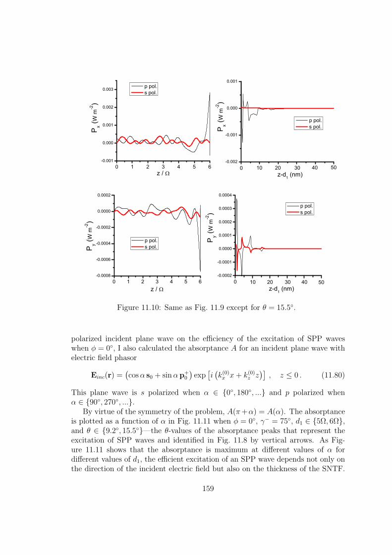
0 1 2 3 4 5 6-0.001
0.000
0.001
0.002
0.003
-0.002
-0.001
0.000
0.001
z /
Px (W
m-2)
p pol. s pol.
Px (W
m-2)
p pol. s pol.
z-d1 (nm)0 10 20 30 40 50
0 1 2 3 4 5 6-0.0008
-0.0006
-0.0004
-0.0002
0.0000
0.0002
-0.0002
-0.0001
0.0000
0.0001
0.0002
0.0003
0.0004
z /
Py (W
m-2)
p pol. s pol.
z-d1 (nm)0 10 20 30 40 50
p pol. s pol.
Py (W
m-2)
Figure 11.10: Same as Fig. 11.9 except for θ = 15.5.
polarized incident plane wave on the efficiency of the excitation of SPP waveswhen ϕ = 0, I also calculated the absorptance A for an incident plane wave withelectric field phasor
Einc(r) =(cosα s0 + sinαp+
0
)exp
[i(k(0)x x+ k(0)z z
)], z ≤ 0 . (11.80)
This plane wave is s polarized when α ∈ 0, 180, ... and p polarized whenα ∈ 90, 270, ....
By virtue of the symmetry of the problem, A(π+α) = A(α). The absorptanceis plotted as a function of α in Fig. 11.11 when ϕ = 0, γ− = 75, d1 ∈ 5Ω, 6Ω,and θ ∈ 9.2, 15.5—the θ-values of the absorptance peaks that represent theexcitation of SPP waves and identified in Fig. 11.8 by vertical arrows. As Fig-ure 11.11 shows that the absorptance is maximum at different values of α fordifferent values of d1, the efficient excitation of an SPP wave depends not only onthe direction of the incident electric field but also on the thickness of the SNTF.
159

0 15 30 45 60 75 90 105 120 135 150 165 1800.05
0.10
0.15
0.20
0.25
0.30
0.35
0.40
0.45
A
(deg)
= 9.2o, d1 = 5
= 9.2o, d1 = 6
= 15.5o, d1 = 5
= 15.5o, d1 = 6
Figure 11.11: Absorptance A vs. α when L = 286 nm, ϕ = 0, γ− = 75,Lg = 20 nm, and d3 − d2 = 30 nm. The electric field phasor of the incident planewave is defined by Eq. (11.80).
To explain this conclusion, let me use Eq. (11.80) in Eq. (11.75) to obtain
A = As cos2 α + Ap sin
2 α +1
2sin 2α
Nt∑n=−Nt
(r(n)ss r
(n)sp
∗+ r(n)ps r
(n)pp
∗+ t(n)ss t
(n)sp
∗
+ t(n)ps t(n)pp
∗+ r(n)ss
∗r(n)sp + r(n)ps
∗r(n)pp + t(n)ss
∗t(n)sp + t(n)ps
∗t(n)pp
)Re
(k(n)z
k(0)z
)(11.81)
Equation (11.81) shows that A depends on α, and more generally, on the vibra-tion ellipse of the incident plane wave. In addition, as depolarization affects theabsorptance and depolarization must depend on d1, the absorptance must also de-pend on the thickness of the SNTF. The higher the absorptance, the more efficientis the excitation of the SPP wave.
11.3.3 Comparison with the TKR configuration
The excitation of multiple SPP waves guided by a planar metal/SNTF interfacein the Kretschmann configuration was studied theoretically earlier in this series[70, 71]. In this configuration, a plane wave propagating in a half space occupied
160
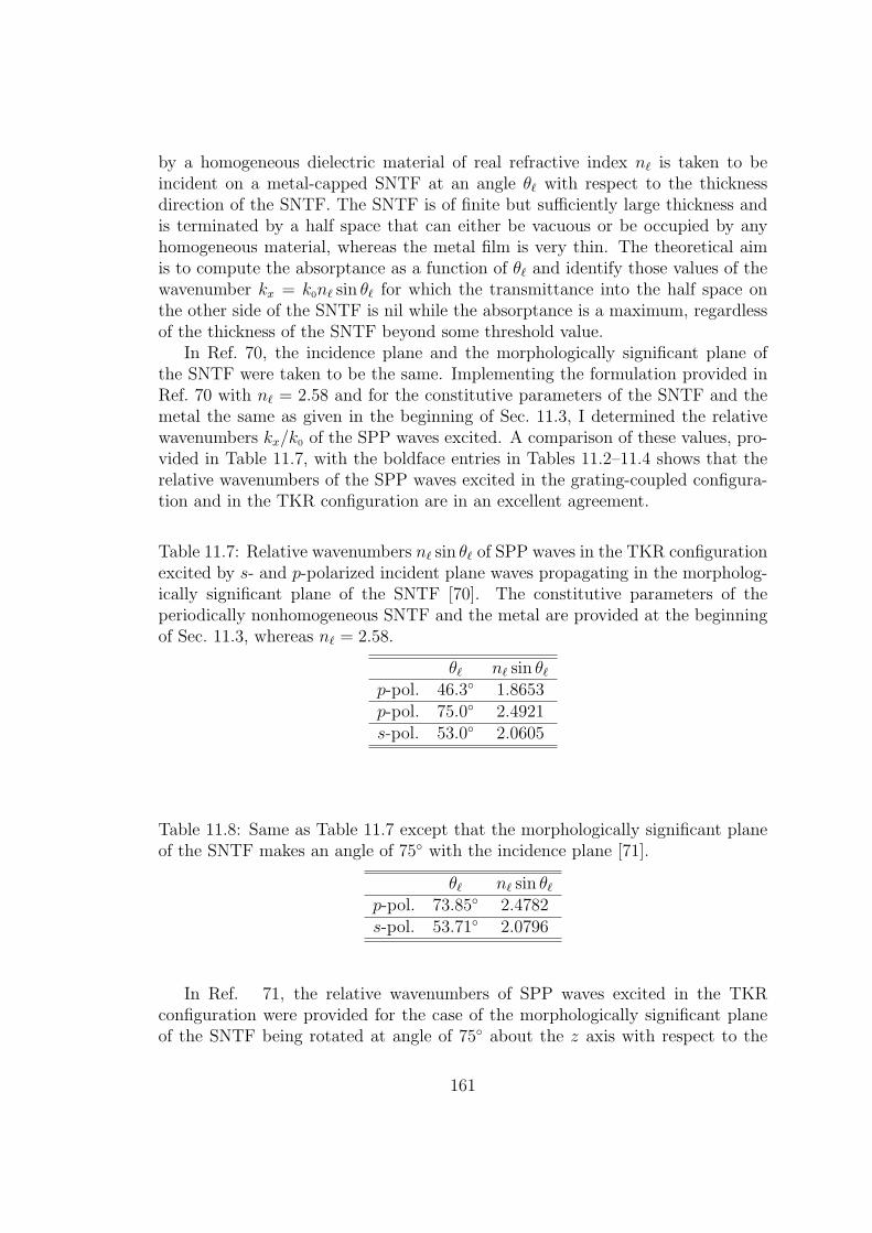
by a homogeneous dielectric material of real refractive index nℓ is taken to beincident on a metal-capped SNTF at an angle θℓ with respect to the thicknessdirection of the SNTF. The SNTF is of finite but sufficiently large thickness andis terminated by a half space that can either be vacuous or be occupied by anyhomogeneous material, whereas the metal film is very thin. The theoretical aimis to compute the absorptance as a function of θℓ and identify those values of thewavenumber kx = k0nℓ sin θℓ for which the transmittance into the half space onthe other side of the SNTF is nil while the absorptance is a maximum, regardlessof the thickness of the SNTF beyond some threshold value.
In Ref. 70, the incidence plane and the morphologically significant plane ofthe SNTF were taken to be the same. Implementing the formulation provided inRef. 70 with nℓ = 2.58 and for the constitutive parameters of the SNTF and themetal the same as given in the beginning of Sec. 11.3, I determined the relativewavenumbers kx/k0 of the SPP waves excited. A comparison of these values, pro-vided in Table 11.7, with the boldface entries in Tables 11.2–11.4 shows that therelative wavenumbers of the SPP waves excited in the grating-coupled configura-tion and in the TKR configuration are in an excellent agreement.
Table 11.7: Relative wavenumbers nℓ sin θℓ of SPP waves in the TKR configurationexcited by s- and p-polarized incident plane waves propagating in the morpholog-ically significant plane of the SNTF [70]. The constitutive parameters of theperiodically nonhomogeneous SNTF and the metal are provided at the beginningof Sec. 11.3, whereas nℓ = 2.58.
θℓ nℓ sin θℓp-pol. 46.3 1.8653p-pol. 75.0 2.4921s-pol. 53.0 2.0605
Table 11.8: Same as Table 11.7 except that the morphologically significant planeof the SNTF makes an angle of 75 with the incidence plane [71].
θℓ nℓ sin θℓp-pol. 73.85 2.4782s-pol. 53.71 2.0796
In Ref. 71, the relative wavenumbers of SPP waves excited in the TKRconfiguration were provided for the case of the morphologically significant planeof the SNTF being rotated at angle of 75 about the z axis with respect to the
161

incidence plane, when nℓ = 2.58 and the constitutive parameters of the SNTFand the metal are the same as in the beginning of Sec. 11.3. These relativewavenumbers are given in Table 11.8, and are in excellent agreement with theboldface entries in Table 11.6 for the grating-coupled configuration.
Besides the agreement of relative wavenumbers of SPP waves in the grating-coupled and the TKR configurations, I noted that in both configurations
(i) the absorptance peaks representing excitation by p-polarized plane wavesare broader than those by s-polarized plane waves; and
(ii) the higher the phase speed of an SPP wave, the narrower is the absorptancepeak representing the excitation of that SPP wave.
Moreover,
(iii) the spatial profiles of SPP waves are similar in both configurations. This canbe seen by comparing Figs. 11.3, 11.5, and 11.7 with Fig. 18 in Ref. 70,1
and Figs. 11.9 and 11.10 in this chapter with Figs. 6 and 3, respectively, inRef. 71.
11.4 Concluding Remarks
The excitation of surface-plasmon-polariton waves by the illumination of a metal-lic surface-relief grating coated with a periodically nonhomogeneous SNTF byan obliquely incident plane wave was theoretically investigated. The absorptanceswere calculated using the rigorous coupled-wave approach as functions of the angleof incidence with respect to the thickness direction of the SNTF and the polar-ization state of the incident plane wave, when the incidence plane and the gratingplane are identical. The excitation of SPP waves was inferred by those peaks inthe absorptance curves
(i) that were independent of the thickness of the SNTF when that thickness issufficiently large;
(ii) where the wavenumber of one of the Floquet harmonics matches that of anSPP wave predicted by the solution of the canonical boundary-value problem(Ch. 2); and
(iii) the spatial profile of the components of time-averaged Poynting vector indi-cated the existence of a surface wave.
1The difference in the values of χv, 45 in this chapter and 30 in Ref. 70, does not create a
significant difference in the spatial profiles.
162

If the morphologically significant plane of the SNTF is parallel to the incidenceplane (and the grating plane), p- and s-polarized SPP waves can be excited, re-spectively, by p- and s-polarized incident plane waves. If the morphologicallysignificant plane is not parallel to the incidence plane, SPP waves that are neitherp nor s polarized can be excited.
In the curves of absorptance as a function of the angle of incidence with respectto the thickness direction of the SNTF,
(i) the peaks representing excitation by incident p-polarized plane waves aregenerally broader than those representing excitation by incident s-polarizedplane waves, and
(ii) the lower the phase speed of an SPP wave, the broader the peaks are in theabsorptance curves.
The efficient excitation of SPP waves depends on the vibration ellipse of theincident plane wave as well as on the thickness of the SNTF.
163

Chapter 12
Conclusions and Suggestions forFuture Work
12.1 Conclusions
As was discussed in Ch. 1, the objectives of the research conducted for this thesiswere to
(a) find the basic property of the partnering dielectric materials that is respon-sible for the multiplicity of surface waves;
(b) elucidate the effects of the morphology of the partnering dielectric materialson the characteristics of surface waves;
(c) find the minimum spatial dimensions of the partnering materials in order toimplement the structures for experimental research;
(d) find other ways to increase the number of possible surface waves;
(e) study the excitation of multiple surface waves in prism- and grating-coupledconfigurations with periodically nonhomogeneous partnering dielectric ma-terials; and
(f) see if multiple SPP waves can lead to enhanced absorption of light in thin-film solar cells.
To achieve these objectives, the propagation and excitation of multiple surfacewaves guided by the interfaces of two dissimilar materials were theoretically stud-ied. The various boundary-value problems investigated are shown in flow diagramin Fig. 12.1 (reproduced from Ch. 1). Two types of surface waves were extensivelystudied: surface plasmon-polariton (SPP) waves, and Dyakonov–Tamm waves.Multiple SPP waves guided by the interface of a metal and a periodically nonho-mogeneous sculptured nematic thin film (SNTF), the interface of a metal and a
164
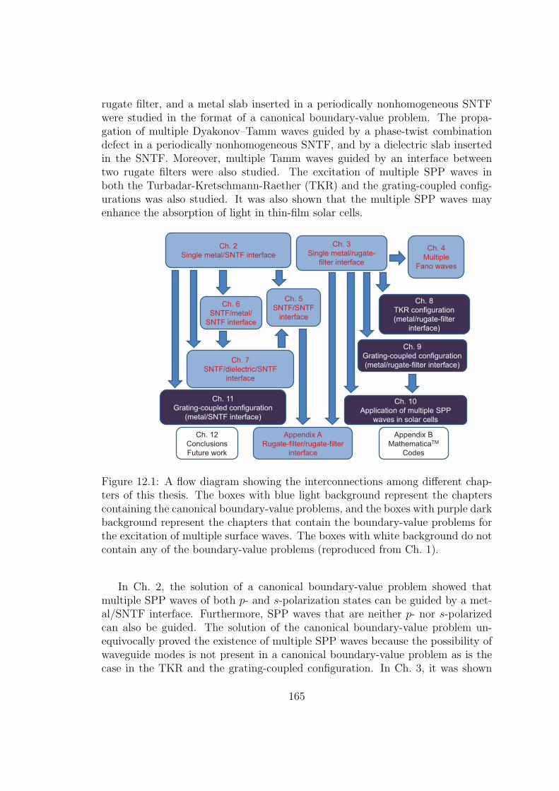
rugate filter, and a metal slab inserted in a periodically nonhomogeneous SNTFwere studied in the format of a canonical boundary-value problem. The propa-gation of multiple Dyakonov–Tamm waves guided by a phase-twist combinationdefect in a periodically nonhomogeneous SNTF, and by a dielectric slab insertedin the SNTF. Moreover, multiple Tamm waves guided by an interface betweentwo rugate filters were also studied. The excitation of multiple SPP waves inboth the Turbadar-Kretschmann-Raether (TKR) and the grating-coupled config-urations was also studied. It was also shown that the multiple SPP waves mayenhance the absorption of light in thin-film solar cells.
Ch. 2
Single metal/SNTF interface
Ch. 3
Single metal/rugate-
filter interface
Ch. 5
SNTF/SNTF
interface
Ch. 7
SNTF/dielectric/SNTF
interface
Ch. 4
Multiple
Fano waves
Ch. 6
SNTF/metal/
SNTF interface
Appendix A
Rugate-filter/rugate-filter
interface
Ch. 8
TKR configuration
(metal/rugate-filter
interface)
Ch. 9
Grating-coupled configuration
(metal/rugate-filter interface)
Ch. 10
Application of multiple SPP
waves in solar cells
Ch. 11
Grating-coupled configuration
(metal/SNTF interface)
Ch. 12
Conclusions
Future work
Appendix B
MathematicaTM
Codes
Figure 12.1: A flow diagram showing the interconnections among different chap-ters of this thesis. The boxes with blue light background represent the chapterscontaining the canonical boundary-value problems, and the boxes with purple darkbackground represent the chapters that contain the boundary-value problems forthe excitation of multiple surface waves. The boxes with white background do notcontain any of the boundary-value problems (reproduced from Ch. 1).
In Ch. 2, the solution of a canonical boundary-value problem showed thatmultiple SPP waves of both p- and s-polarization states can be guided by a met-al/SNTF interface. Furthermore, SPP waves that are neither p- nor s-polarizedcan also be guided. The solution of the canonical boundary-value problem un-equivocally proved the existence of multiple SPP waves because the possibility ofwaveguide modes is not present in a canonical boundary-value problem as is thecase in the TKR and the grating-coupled configuration. In Ch. 3, it was shown
165
that multiple SPP waves can be guided by an interface of a metal and a period-ically nonhomogeneous dielectric material even if that material is isotropic. Thiswas an important discovery as it showed that it is the periodic nonhomogeity ofthe partnering dielectric material that is responsible for the multiplicity of SPPwaves provided that the period of the dielectric material is within a certain rangeof values. The results obtained in Ch. 3 proved to be a cornerstone for most ofthe research conducted by me.
In Ch. 4, it was seen that SPP waves transmute into Fano waves when theimaginary part of the permittivity of the partnering metal is made zero. Moreover,the nonhomogeneity of the partnering dielectric material led to the excitation ofnot one but multiple Fano waves, supporting further the hypothesis that periodicnonhomogeneity of the dielectric material leads towards multiple surface waves.
To further increase the number of possible surface waves, it was hypothesizedthat two interfaces in close proximity could lead to new surface waves. For thispurpose, the canonical boundary-value problem of SPP wave-propagation by anSNTF/metal/SNTF system was solved in Ch. 6. The solution of the canonicalproblem showed that the coupling of the two metal/SNTF interfaces results innew SPP waves provided the metallic layer between the two SNTFs is thinnerthan twice the penetration depth of the SPP waves into the metal. In Ch. 7,the effect of coupling on the Dyakonov–Tamm waves was studied by solving acanonical problem of SNTF/dielectric/SNTF system. Again, it was seen that asufficiently thin dielectric layer can lead to new Dyakonov–Tamm waves that wereotherwise absent from the single dielectric/SNTF interface. Moreover, waveguidemodes were also found to be guided by the dielectric slab in addition to the surfacewaves. Propagation guided by the SNTF/dielectric/SNTF system is lossless (oralmost lossless with actual materials), but not by the SNTF/metal/SNTF sys-tem. However, one slight disadvantage of the SNTF/dielectric/SNTF system isthe shorter angular sector—when both the interfaces are uncoupled—for the prop-agation directions of Dyakonov–Tamm waves when compared to SPP waves. Thecapability for lossless propagation of surface waves in any direction could be usefulfor sensing and communication applications that are currently restricted by the at-tenuative propagation of SPP waves [14,34,35,40,41]. Multiple Dyakonov–Tammwaves can lead to enhanced confidence in sensing measurements and may increasethe capabilities of multi-analyte sensors. The coexistence of the Dyakonov–Tammwaves and the waveguide modes could lead to enhanced sensing modalities. Thepresence of multiple Dyakonov–Tamm waves and waveguide modes may also beuseful for multi-channel communication at a specific frequency.
The excitation of multiple SPP waves in the TKR configuration was studiedin Ch. 8. A plane wave of either p- or s-polarization state, propagating in anoptically denser dielectric material, was taken to be incident on a metal-cappedrugate filter. The absorptances were calculated using a stable numerical algorithmas functions of the incidence angle. The excitation of SPP waves was inferred from
166

the presence of those peaks in the absorptance spectrum that were independent ofthe thickness of the rugate filter. A canonical boundary-value problem to studythe propagation of coupled SPP waves by a metal film, with a semi-infinite rugatefilter on one side and a semi-infinite homogeneous dielectric material on the otherside, was also formulated to obtain a dispersion equation for each of the twolinear polarization states. The solution of the dispersion equations and the spatialprofiles of the SPP waves showed that p-polarized SPP waves are more likelyto couple to the prism/metal interface than s-polarized SPP waves. However,the solution of another canonical boundary-value problem (Ch. 3) of SPP-wavepropagation by the interface of a semi-infinite metal and a semi-infinite rugate filterrevealed that the coupling due to the thin metal film in the TKR configurationdoes not result in new SPP waves.
The excitation of multiple SPP waves by a surface-relief grating formed by ametal and a dielectric material, both of finite thickness, was studied theoreticallyin Ch. 9 using the rigorous coupled-wave approach (RCWA) for a practically im-plementable setup. The presence of an SPP wave was inferred by a peak in theplot of absorptance vs. the angle of incidence θ, provided that the θ-location ofthe peak turned out to be independent of the thickness of the dielectric partner-ing material. If that material is homogeneous, only one p-polarized SPP wave,that too of p-polarization state, is excited. In general, the absorptance peak isnarrower for an s-polarized SPP wave than for of a p-polarized SPP wave, andthe absorptance peak is narrower for an SPP wave of higher phase speed. Thefact that only p-polarized SPP waves can be excited when the partnering dielec-tric material is homogeneous indicates the difficulty of exciting s-polarized SPPwaves—which is reflected both in the narrower peaks for As than for Ap in theresults presented in Chs. 8, 9, 10, and 11, as well as in the greater number ofsolutions of a relevant canonical boundary-value problem in Ch. 3 for p- than fors-polarized SPP waves. Underlying all of these observations is the great mismatchin optical admittance [33] across metal/dielectric interfaces that usually prevailsfor s-polarized fields [48].
In Ch. 10, the excitation of multiple SPP waves was shown to increase theabsorption in thin-film solar cells. For the chosen semiconductor material andthe metal, it was seen that periodically corrugated metallic back surface may leadto excitation of both p- and s-polarized SPP waves, thereby, increasing the over-all absorption in the structure. Though, the excitation of waveguide modes alsoplays a role in the enhancement of absorption in the grating-coupled configuration.However, the geometric parameters of the surface-relief grating and the periodi-cally nonhomogeneous semiconductor layer shall have to be optimized carefully inorder to obtain an overall enhanced absorption of the insolation flux over the 400–1200-nm wavelength range. I hope that this work will turn out to be a useful firststep towards the exploitation of multiple SPP waves in enhancing the efficiency ofthin-film solar cells.
167

Finally, the excitation of SPP waves guided by a metal/SNTF interface wasinvestigated in Ch. 11. The results obtained in this chapter not only reinforced theconclusions drawn by the investigations on the related canonical boundary-valueproblem, but also opened routes towards the excitation of multiple SPP wavesguided by the interface of a metal and a periodically nonhomogeneous SNTF.It was seen that efficient excitation of SPP waves does not only depend on thepolarization ellipse of the incident linearly polarized plane wave but also on thethickness of the SNTF. So, optimization of the grating profile and the SNTFthickness may be necessary for efficient simultaneous excitation of many SPPwaves as well as for broadband performance.
The excitation of different SPP waves in the grating-coupled configurationsometimes requires different periods of the surface-relief grating, as was seen inChs. 9, 10, and 11. Therefore, the simultaneous excitation of all possible SPPwaves may be achieved using a quasi-periodic grating [131].
In summary, it was found that
(i) it is the periodic nonhomogeneity (not the anisotropy) of the partneringdielectric material normal to the interface that is responsible for the multi-plicity of surface waves;
(ii) multiple SPP, Tamm, Dyakonov–Tamm, and Fano waves of the same fre-quency and different phase speeds and spatial profiles can be guided by aninterface of two different materials provided that at least one of them isperiodically nonhomogeneous normal to the interface;
(iii) the morphology of the partnering dielectric material affects the number,the phase speeds, the spatial profiles, and the degrees of localization of thesurface waves;
(iv) the number of surface waves can be increased further by the coupling of twointerfaces separated by a sufficiently thin layer;
(v) multiple surface waves can be excited in the TKR and the grating-coupledconfigurations with periodically nonhomogeneous dielectric materials; and
(vi) multiple SPP waves can be used to enhance the light absorption in a thin-filmsolar cell.
These conclusions relate to objectives (a)-(f) in the same order.Since a variety of theoretical problems of practical significance have been for-
mulated and solved in this thesis, it is hoped that it will provide a rigorous the-oretical footing for later research on the exploitation of multiple surface waves inoptical applications.
Let me conclude by noting that all computations in this thesis were madeat a single free-space wavelength λ0 (except in Ch. 10, where two values of λ0
168

were considered); however, multiple SPP waves can be expected at other valuesof λ0 too. The numbers of p- and s-polarized SPP waves and their wavenumbersin any related canonical boundary-value problem must depend on λ0. This isbecause all constitutive parameters of causal materials are frequency-dependent,not to mention that the effects of the spatial dimensions of the materials requireinterpretation in terms of λ0.
12.2 Suggestions for Future Work
The study of multiple surface waves is still in its infancy, and there is considerableroom available to work both theoretically and experimentally, and both to gainunderstanding of the phenomenon of multiplicity and its exploitation for practicaldevices. I have a few suggestions for theoretical work on multiple surface wavesbased on the work reported in this thesis.
12.2.1 Excitation of multiple surface waves with a finitesource
The study of excitation of multiple surface waves with a finite source, such as aline source, in either the TKR or the grating-coupled configuration will not onlyincrease the scope of applications of surface waves but can also provide a routetowards exciting multiple surface waves without the inconvenience of changingthe angle of incidence. This study can lead to the possibility of exciting multiplesurface waves in nano-devices with embedded light sources. This problem canbe analyzed easily by expressing the electromagnetic field of the finite source asa spectrum of planewaves [132, Sec. 2.2], and utilizing the same analytical andnumerical tools explained in Chs. 8, 9, and 11.
12.2.2 Simultaneous excitation of all possible SPP wavesusing quasi-periodic surface-relief grating
As was seen in Chs. 9, 10, and 11 that the excitation of different SPP waves requiresthat different choices may be needed for the period of the surface-relief grating.This is impossible to achieve with one fixed structure but can be overcome byhaving a new surface-relief grating such that each period of the new surface-reliefgrating contains, say, two or three periods of two (or as many as one likes) differentsurface-relief gratings. This new structure will allow the simultaneous excitationof all possible SPP waves without having to change anything. This problem canbe tackled with the formulations provided in Chs. 9 and 11 by taking a newgrating shape-function g(x). However, for computations, the number of terms in
169

the Fourier expansion of the grating shape-function g(x) needs to be much higherthan what was used in Chs. 9 and 11 in order to get converged solutions.
12.2.3 Excitation of Tamm and Dyakonov–Tamm waves
As was described in the introduction to Ch. 7, the scope of application of SPPwaves is limited due to the propagation losses along the direction of propagation.This limitation can be overcome by having the ability to excite other types ofsurface waves, that is, Tamm and Dyakonov–Tamm waves. These waves propa-gate with negligible losses. So, the problem of excitation of multiple Tamm andDyakonov–Tamm waves is very important to enhance the scope of applications ofmultiple surface waves. The study of excitation of Tamm and Dyakonov–Tammwaves can be done with the same formulation as provided in Chs. 8, 9, and 11:just the permittivity of the metal layers in those chapters needs to be replaced bythe permittivity of the chosen dielectric materials.
12.2.4 Thin-film solar cell with actual configuration
In Ch. 10, it was seen that the light absorption can be enhanced if the partneringsemiconductor material in the grating-coupled configuration is made periodicallynonhomogeneous normal to the mean metal/semiconductor interface. However,the boundary value problem in that chapter can not be used for actual solar cellsbecause it does not have any p− n junctions and no antireflection (AR) coatingsor transparent conducting oxide (TCO) layer for electrical connection. Moreover,the problem solved in that chapter was limited only to the enhancement of lightabsorption and not the output power. I believe, a complete problem that includethe geometry of actual solar cell with the aim to optimize the output power isworth investigating. For this purpose, the formulation given in Ch. 9 will have tobe modified in order to include layered structure of the solar cell.
170

Appendix A
Propagation of Multiple TammWaves‡
A.1 Introduction
The reports on the propagation of surface waves when both partnering dielec-tric materials are periodically nonhomogeneous normal to the interface are muchscarcer and of very recent vintage [65–68, 133, 134]. In all of these reports, bothpartnering materials are also anisotropic. Numerical studies have shown that,depending on the direction of propagation in the interface plane, from none upto four surface waves—with different phase speeds, spatial distributions of theelectromagnetic field components, and degrees of localization—can propagate ata particular frequency and for a chosen set of partnering materials. Would similarcharacteristics be exhibited if both partnering materials were isotropic, in contrastto those in previous works in Refs. 65–68,133, and 134, and in Ch. 5 of this thesis?The work reported in this appendix was undertaken to satisfy that curiosity.
The isotropic but periodically nonhomogeneous material chosen for this pur-pose has a refractive index that varies sinusoidally about a mean value. Suchcontinuously nonhomogeneous materials are routinely used as rugate filters forrejecting light in a specific frequency band [2, 74] and may have application insolar cells too [75]. Because of analogy with the surface Tamm states [61, 62] insolid-state electronics, the surface waves supported by rugate filters—and otherperiodically nonhomogeneous materials such as the piecewise homogeneous pho-tonic crystals [135, 136]—are called Tamm waves [16, 137]. However, a subset ofthese can also be classified as optical Tamm states [138].
A synoptic view of the canonical problem of surface waves supported by theinterface of two distinct, semi-infinite rugate filters with sinusoidal refractive-index
‡This appendix is based on: H. Maab, M. Faryad, and A. Lakhtakia, “Surface electromagneticwaves supported by the interface of two semi-infinite rugate filters with sinusoidal refractive indexprofiles,” J. Opt. Soc. Am. A 28, 1204–1212 (2011).
171

profiles is provided here. The two filters can differ in the mean refractive index,the amplitude of the refractive-index modulation, and the period of the same mod-ulation. Alternatively, the two rugate filters can be identical except for a phasedefect [65–67]. Since surface waves generally decay away from the interface, thecanonical problem involving two semi-infinite rugate filters can be practically im-plemented using two rugate filters of sufficient thickness. Surface waves can beexcited using an end-fire coupling technique [41] involving either a diffraction grat-ing [14] or a fiber [35]. Section A.2 provides the necessary theoretical formulation,while numerical results are presented and discussed in Section A.3. Finally, theconcluding remarks are presented in Sec. A.4.
A.2 Theory
Let the refractive index at the chosen angular frequency ω for all z ∈ (−∞,∞) bespecified as
n(z) =
n−(z) = n−
avg + (∆−n /2) sin(ϕ
− + πz/Ω−) , z < 0 ,n+(z) = n+
avg + (∆+n /2) sin(ϕ
+ + πz/Ω+) , z > 0 ,(A.1)
so that n±(z±2Ω±) = n±(z). Here, n±avg are the mean refractive indexes, whereas
∆n±, 2Ω±, and ϕ±, respectively, are the amplitudes, periods, and phases of therefractive-index modulation. Other periodic profiles of n±(z) can also be accom-modated by the formulation described in this section.
Without any loss of generality, I take the propagation direction in the interfaceplane z = 0 to be parallel to the x axis. Since both dielectric materials areisotropic, the surface waves are either s-polarized or p-polarized. These two typesof surface waves can be handled separately.
A.2.1 s-polarized surface waves
For an s-polarized surface wave, I have
E(r) = ey(z)uy exp (iκx)
andH(r) = [hx(z)ux + (κ/k0η0) ey(z)uz] exp (iκx) ,
where ω/Re(κ) is the phase speed of the surface wave along the x axis. Further-more, the frequency-domain Maxwell equations yield the matrix ordinary differ-ential equation
d
dz
[ey(z)
hx(z)
]= −iω
0 µ0
ϵ0
[n2(z)−
(κk0
)2]0
·
[ey(z)
hx(z)
], z = 0 . (A.2)
172
Equation (A.2) has to be solved in order to determine the matrixes[Q±]that
appear in the relations[ey(±2Ω±)
hx(±2Ω±)
]=[Q±]·
[ey(0±)
hx(0±)
](A.3)
and characterize the optical responses of one period of the rugate filters on the twosides of the interface. These matrixes can be calculated using standard numericaltechniques [65, 89]. Thereafter, the eigenvalues σ±
1 and σ±2 = 1/σ±
1 , and the cor-
responding eigenvectors[1, t±1
]Tand
[1, t±2
]T, of
[Q±]can be calculated, where
the eigenvalues and the eigenvectors have been labeled such that Re(lnσ±
1
)< 0
(Ch. 5). Consistent with the requirement that the electromagnetic field mustdecay as z → ±∞, I get [136][
ey(0±)
hx(0±)
]= a±
[1
t±1
], (A.4)
where a± are unknown coefficients. As the usual boundary conditions must holdacross the interface z = 0—i.e., ey(0+) = ey(0−) and hx(0+) = hx(0−)—I obtain[
1 −1
t+1 −t−1
]·
[a+
a−
]=
[0
0
], (A.5)
which yields the identity a+ = a− and the dispersion equation
t+(κ) = t−(κ) (A.6)
for the s-polarized surface wave.
A.2.2 p-polarized surface waves
For a p-polarized surface wave, I have
H(r) = hy(z)uy exp (iκx)
andE(r) =
ex(z)ux −
[κη0/k0n
2(z)]hy(z)uz
exp (iκx) .
Furthermore, the frequency-domain Maxwell equations yield the matrix ordinarydifferential equation
d
dz
[ex(z)
hy(z)
]= iω
0 µ0
n2(z)
[n2(z)−
(κk0
)2]ϵ0n
2(z) 0
·
[ex(z)
hy(z)
], z = 0 .
(A.7)The remainder of the procedure to determine the dispersion equation of the p-polarized surface wave is exactly the same as in Section A.2.1.
173
A.3 Numerical Results and Discussion
A computer program was prepared to find the solutions of the dispersion equationsof s− and p-polarized surface waves, using the Newton–Raphson method [89]. Allcalculations were made for λ0 = 633 nm. Several different cases were solved inorder to understand the characteristics of surface waves supported by rugate filterswith sinusoidal refractive-index profiles. The search for solutions was confined toreal-valued κ, because all refractive indexes were taken to be real-valued.
A.3.1 Homogeneous-dielectric/rugate-filter interface
Let me begin with surface-wave propagation guided by the interface of a homoge-neous dielectric material (z < 0) and a rugate filter (z > 0). For this purpose, letme set ∆−
n = 0 and ϕ+ = 0.Figure A.1 shows the solutions κ/k0 of the dispersion equations for Tamm
waves of both linear polarization states when n+avg = 1.885, ∆+
n = 0.87, Ω+ = λ0,and ϕ+ = 0, while n−
avg ∈ [1.3, 2.2]; parenthetically, I note that these parametersfor a rugate filter are realizable [74]. The immediately obvious conclusion fromthe figure is that more than one solutions are possible. The number of solutionsdecreases as n−
avg increases towards the maximum value n+avg + ∆+
n /2 of n+(z).Thus, in Fig. A.1, only two solutions exist for the highest value of n−
avg althougheight solutions exist for the lowest value of n−
avg.The multiplicity of solutions in Fig. A.1 is just like that for surface-plasmon-
polariton (SPP) waves guided by the interface of a metal and a rugate filter (Ch. 3).However, whereas those SPP waves are much more likely to be p-polarized thans-polarized as was seen in Ch. 3, the polarization states of Tamm waves here arealmost equally—but not always equally—split between s and p.
The presented data also show that the phase speed of a Tamm wave is smallerthan the phase speed in the homogeneous partnering material, because κ > k0n
−avg.
Furthermore, as k0(n+avg −∆+
n /2) < κ < k0(n+avg +∆+
n /2), the phase speed of theTamm wave is intermediate to both the minimum and the maximum phase speedsin the rugate filter. Exploration of the κ-range beyond k0(n
+avg +∆+
n /2) failed toturn up solutions.
For a fixed value of n−avg, the different Tamm waves have distinct phase speeds.
They also have different spatial distributions of the components of the electro-magnetic field despite the identity a+ = a−. Figure A.2 shows field distributionprofiles for three of the eight Tamm waves for n−
avg =√2, the other parameters
being the same as for Fig. A.1. Inside the homogeneous partnering material, thenonzero field components decay exponentially as z → −∞, the variation being
of the type exp
[z√κ2 −
(k0n−
avg
)2]with κ > k0n
−avg. Thus, the higher the value
of κ (i.e., the lower the phase speed) at fixed n−avg, the more tightly bound is the
174

1.3 1.4 1.5 1.6 1.7 1.8 1.9 2.0 2.1 2.21.5
1.6
1.7
1.8
1.9
2.0
2.1
2.2
2.3
/ k0
n-avg
Figure A.1: κ/k0 versus n−avg for Tamm waves localized to the interface of a homo-
geneous dielectric material (∆−n = 0) and a rugate filter (n+
avg = 1.885, ∆+n = 0.87,
Ω+ = λ0, and ϕ+ = 0), when the free-space wavelength λ0 = 633 nm. The redcircles indicate s-polarized Tamm waves and the black triangles are for p-polarizedTamm waves. I failed to find solutions to bridge the gaps in two branches of solu-tions; these gaps are likely to be numerical artefacts, as there is no physical reasonfor them to exist.
Tamm wave to the plane z = 0−.In contrast, the field distribution has to be far more complicated inside the
rugate filter (z > 0). Following the dictates of the Floquet–Lyapunov theorem [88],the z-dependence of each nonzero component of the electromagnetic field is theproduct of two factors. One of these factors decays exponentially as z → ∞, butthe other factor is faithfully reproduced unit cell by unit cell. The undulations ofthe second factor in each unit cell can be cast in terms of a semiclassical coupledwave theory [139, 140]. Hence, in Fig. A.2, the average of a nonzero componentover the q-th unit cell z ∈ [2(q − 1)Ω+, 2qΩ+] is higher than the average over the(q+1)-th unit cell z ∈ [2qΩ+, 2(q + 1)Ω+], q ∈ 1, 2, ..., but the variations insidetwo adjacent unit cells look quite similar in form.
The maximum field strength of a Tamm wave does not necessarily lie at theinterface plane. Thus, in Fig. A.2, the maximum magnitudes inside the rugate
175

-2 0 2 4 60
0.2
0.6
1
1.4
zW+
e 8x,
y,z<
-2 0 2 4 60
0.001
0.003
0.005
0.007
zW+
h 8x,
y,z<
-2 0 2 4 60
0.4
0.8
1.2
zW+
e 8x,
y,z<
-2 0 2 4 60
0.001
0.003
0.005
zW+h 8
x,y,
z<
-2 0 2 4 60
2
4
6
8
10
zW+
e 8x,
y,z<
-2 0 2 4 60
0.02
0.04
0.06
zW+
h 8x,
y,z<
Figure A.2: Variation of the magnitudes of the nonzero Cartesian components of(left) E (in V m−1) and (right) H (in A m−1) of Tamm waves along the z axis,when λ0 = 633 nm, n−
avg =√2, ∆−
n = 0, n+avg = 1.885, ∆+
n = 0.87, Ω+ = λ0,and ϕ+ = 0. The components parallel to ux, uy, and uz are represented by reddotted, blue dashed, and black solid lines, respectively. All calculations were madeafter setting a+ = a− = 1 V m−1. (top) p-polarization state and κ/k0 = 1.5286,(middle) s-polarization state and κ/k0 = 1.5430, and (bottom) s-polarization stateand κ/k0 = 2.2143.
filter lie at z ≃ 1.4Ω+ in the plots in the top and middle rows, and at z = 0.5Ω+
in the bottom row.In order to quantify the degree of localization of the Tamm wave to the
plane z = 0+, let me define the decay constant β+ = exp[Re(lnσ+
1
)]. Since
Re (ln σ+) < 0, and thus 0 < β+ < 1; the smaller the decay constant is, thestronger is the Tamm wave localized to the interface. The decay constant of thep-polarized Tamm wave (top row in Fig. A.2) is β+ = 0.2437, while the decayconstants of the two s-polarized Tamm waves are β+ = 0.1881 (middle row) and
176

β+ = 0.0005 (bottom row), respectively. These values of β+ illustrate the weakerlocalization of the p-polarized Tamm wave in comparison to the stronger localiza-tion of the two s-polarized Tamm waves, in Fig. A.2.
The effect of the amplitude ∆+n of the refractive-index modulation of the rugate
filter was examined next. For this purpose, calculations were made with n−avg =√
2.5, Ω+ = λ0, and n+avg = 1.885 fixed, while ∆+
n ≤ 2. No solutions can exist for∆+
n = 0 because both the partnering materials then are homogeneous with relativepermittivities that are positive and real-valued [14,35], and none was found. Thesmallest value of ∆+
n for which a solutions was found is 0.01; the solution is for thes-polarization state, as shown in Fig. A.3. The smallest value of ∆+
n is a physicalrequirement in order for the discontinuity at the interface to be able to guide asurface wave. Fewer solutions are present for lower values than for the highervalues of ∆+
n . For lower values of ∆+n , the decay constant β+ is close to unity
signifying that the Tamm waves are weakly bound to the interface z = 0+; as ∆+n
increases, β+ decreases signifying more tightly bound Tamm waves. Furthermore,solutions with higher phase speed ω/κ emerge and the phase-speed distributiongenerally widens as ∆+
n increases.In order to investigate the role of the period of the rugate filter, the same ex-
ercise as for Fig. A.3 was conducted, except that ∆+n = 0.87 was fixed but Ω+/λ0
was varied between 0 and 2.0. As Fig. A.4 shows, the number of solutions is gen-erally small when the period of the rugate filter is small. I were not able to findany solutions of the dispersion equations when Ω+ < 0.32λ0. This limit suggests aphysical restriction on the minimum value of the period in order for a surface waveto be guided by the interface of a homogeneous material and a periodically non-homogeneous material. As the period 2Ω+ increases, more solutions can emerge,but there is an upper limit to the number of solutions since all solutions in thefigure are confined to the range k0(n
+avg −∆+
n /2) < κ < k0(n+avg +∆+
n /2). Furtherincrease of the period 2Ω+ should lead to a decrease in the number of solutions;indeed, when 2Ω+ is very large, the periodically nonhomogeneous material be-comes virtually homogeneous close to the interface and no surface wave can thenbe supported.
A.3.2 Rugate filter with a phase defect
If n−avg = n+
avg, ∆−n = ∆+
n , Ω− = Ω+, but ϕ− = ϕ+, one can say that the entire
space z ∈ (−∞,∞) is occupied by a single rugate filter which has a phase defectϕ+ − ϕ− at the plane z = 0. I chose to investigate the propagation of Tammwaves guided by the phase defect at λ0 = 633 nm by fixing n−
avg = n+avg = 1.885,
∆−n = ∆+
n = 0.87, Ω− = Ω+ = λ0, ϕ+ = 0, but keeping ϕ− ∈ [0, 2π) variable.
Clearly, n(z) is continuous across the plane z = 0, and the phase defect vanishes,when ϕ− = 0 or 2π. In contrast, a phase defect does exist despite the continuity ofn(z) across the plane z = 0 when ϕ− = π; however, I could not find any solutions
177

0.2 0.4 0.6 0.8 1.0 1.2 1.4 1.6 1.8 2.0
1.6
1.7
1.8
1.9
2.0
2.1
2.2
2.3
2.4
2.5
2.6
/ k0
+n
0.01
Figure A.3: κ/k0 versus ∆+n for Tamm waves localized to the interface of a homoge-
neous dielectric material (n−avg =
√2.5, ∆−
n = 0) and a rugate filter (n+avg = 1.885,
Ω+ = λ0, and ϕ+ = 0), when the free-space wavelength λ0 = 633 nm. The redcircles indicate s-polarized Tamm waves and the black triangles are for p-polarizedTamm waves.
of the dispersion equations that signifies Tamm waves. For other values of ϕ−,n(z) is discontinuous across the plane z = 0.
The solutions of the dispersion equations for Tamm waves bound to the phase-defect plane z = 0 are shown in Fig. A.5. Clearly, multiple Tamm waves can beguided by a phase defect in a rugate filter. For ϕ− /∈ 0, π, up to 12 solutions arepossible with κ > k0(n
+avg −∆+
n /2), almost always equally divided between the s-and p-polarization states. As ϕ− increases from 0, the number of solutions increasesepisodically. All branches of s-polarized solutions are paired with branches of p-polarized solutions, and all of these solutions satisfy the inequality κ > k0(n
+avg −
∆+n /2).Four unpaired branches of p-polarized solutions also exist in Fig. A.5. One
branch satisfies the inequality κ > k0(n+avg−∆+
n /2) and therefore indicates Tamm-wave propagation. For the other three unpaired branches, κ < k0(n
+avg − ∆+
n /2).Solutions on these three branches are special because κ/k0 is less than the mini-mum value of the refractive index of the rugate filter on either side of the phase
178
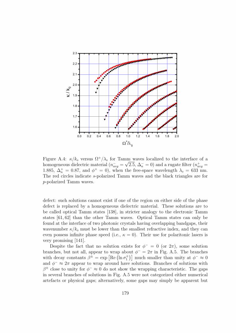
0.0 0.2 0.4 0.6 0.8 1.0 1.2 1.4 1.6 1.8 2.0
1.6
1.7
1.8
1.9
2.0
2.1
2.2
2.3
/ k
0
+/ 0
Figure A.4: κ/k0 versus Ω+/λ0 for Tamm waves localized to the interface of ahomogeneous dielectric material (n−
avg =√2.5, ∆−
n = 0) and a rugate filter (n+avg =
1.885, ∆+n = 0.87, and ϕ+ = 0), when the free-space wavelength λ0 = 633 nm.
The red circles indicate s-polarized Tamm waves and the black triangles are forp-polarized Tamm waves.
defect: such solutions cannot exist if one of the region on either side of the phasedefect is replaced by a homogeneous dielectric material. These solutions are tobe called optical Tamm states [138], in stricter analogy to the electronic Tammstates [61, 62] than the other Tamm waves. Optical Tamm states can only befound at the interface of two photonic crystals having overlapping bandgaps, theirwavenumber κ/k0 must be lower than the smallest refractive index, and they caneven possess infinite phase speed (i.e., κ = 0). Their use for polaritonic lasers isvery promising [141].
Despite the fact that no solution exists for ϕ− = 0 (or 2π), some solutionbranches, but not all, appear to wrap about ϕ− = 2π in Fig. A.5. The brancheswith decay constants β± = exp
[Re(lnσ±
1
)]much smaller than unity at ϕ− ≈ 0
and ϕ− ≈ 2π appear to wrap around have solutions. Branches of solutions withβ± close to unity for ϕ− ≈ 0 do not show the wrapping characteristic. The gapsin several branches of solutions in Fig. A.5 were not categorized either numericalartefacts or physical gaps; alternatively, some gaps may simply be apparent but
179

30 60 90 120 150 180 210 240 270 300 330
1.4
1.5
1.6
1.7
1.8
1.9
2.0
2.1
2.2
/ k0
-(deg)
0.02 359.9
Figure A.5: κ/k0 versus ϕ− for Tamm waves localized to the phase-defect plane z =
0 in a rugate filter, with n+avg = n−
avg = 1.885, ∆+n = ∆−
n = 0.87, Ω+ = Ω− = λ0,and ϕ+ = 0, when the free-space wavelength λ0 = 633 nm. The red circles indicates−polarized Tamm waves and the black triangles are for p-polarized Tamm waves.No solutions exist for ϕ− ∈ 0, π.
not real.The eigenvalues σ±
1,2 depend on the matrixes[Q±], which are responses of one
period of the rugate filter on either side of the interface. As the same rugate filter
exists on both sides of a phase defect interface,[Q+]and
[Q−]are related such
that σ+ℓ = σ−
ℓ , ℓ ∈ 1, 2; hence, β+ = β−, and the decay constants on either sideof the phase-defect interface are identical.
Spatial profiles of the electromagnetic field are shown in Fig. A.6 for two p-polarized Tamm waves at ϕ− = 8 and 174, and one s-polarized Tamm wave atϕ− = 8. The decay constants at ϕ− = 8 for the p-polarized wave are β+ = β− =0.2821, and for the s-polarized wave are β+ = β− = 0.0221. The decay constantsat ϕ− = 174 for the p-polarized wave are β+ = β− = 0.3240. Of these threeTamm waves, the s-polarized wave is most strongly localized to the phase-defect
180

-6 -4 -2 0 2 4 60
1
2
3
4
zW+
e 8x,
y,z<
-6 -4 -2 0 2 4 60.000
0.005
0.010
0.015
0.020
zW+
h 8x,
y,z<
-6 -4 -2 0 2 4 60.0
0.2
0.4
0.6
0.8
1.0
zW+
e 8x,
y,z<
-6 -4 -2 0 2 4 60.000
0.001
0.002
0.003
0.004
0.005
zW+h 8
x,y,
z<
-6 -4 -2 0 2 4 602468
101214
zW+
e 8x,
y,z<
-6 -4 -2 0 2 4 60.00
0.02
0.04
0.06
0.08
zW+
h 8x,
y,z<
Figure A.6: Variation of the magnitudes of the nonzero Cartesian components of(left) E (in V m−1) and (right) H (in A m−1) of Tamm waves along the z axis.All parameters are same as for Fig. A.5 except ϕ− = 8 for the top and middlerows, and ϕ− = 174 for the bottom row. The components parallel to ux, uy, anduz are represented by red dotted, blue dashed, and black solid lines, respectively.All calculations were made after setting a+ = a− = 1 V m−1. (top) p-polarizationstate and κ/k0 = 1.6155, (middle) s-polarization state and κ/k0 = 1.8007, and(bottom) p-polarization state and κ/k0 = 1.5718.
interface.Figure A.7 shows the spatial profile of the electromagnetic field at ϕ− = 30
for a p-polarized optical Tamm state. The value of κ/k0 is less than the minimumvalue of the refractive index on either side of the phase-defect interface. The decayconstants are β+ = β− = 0.7765, which indicate weak localization to the interface
181
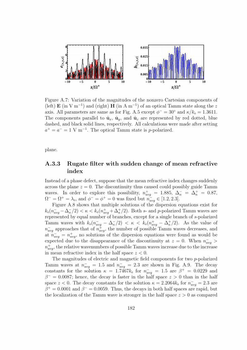
-10 -5 0 5 100
2
4
6
8
zW+
e 8x,
y,z<
-10 -5 0 5 100
0.005
0.015
0.025
0.035
zW+
h 8x,
y,z<
Figure A.7: Variation of the magnitudes of the nonzero Cartesian components of(left) E (in V m−1) and (right) H (in A m−1) of an optical Tamm state along the zaxis. All parameters are same as for Fig. A.5 except ϕ− = 30 and κ/k0 = 1.3611.The components parallel to ux, uy, and uz are represented by red dotted, bluedashed, and black solid lines, respectively. All calculations were made after settinga+ = a− = 1 V m−1. The optical Tamm state is p-polarized.
plane.
A.3.3 Rugate filter with sudden change of mean refractiveindex
Instead of a phase defect, suppose that the mean refractive index changes suddenlyacross the plane z = 0. The discontinuity thus caused could possibly guide Tammwaves. In order to explore this possibility, n+
avg = 1.885, ∆−n = ∆+
n = 0.87,Ω− = Ω+ = λ0, and ϕ
− = ϕ+ = 0 was fixed but n−avg ∈ [1.2, 2.3].
Figure A.8 shows that multiple solutions of the dispersion equations exist fork0(n
−avg−∆−
n /2) < κ < k0(n+avg+∆+
n /2). Both s- and p-polarized Tamm waves arerepresented by equal number of branches, except for a single branch of s-polarizedTamm waves with k0(n
−avg − ∆−
n /2) < κ < k0(n+avg − ∆+
n /2). As the value ofn−avg approaches that of n+
avg, the number of possible Tamm waves decreases, andat n−
avg = n+avg, no solutions of the dispersion equations were found as would be
expected due to the disappearance of the discontinuity at z = 0. When n−avg >
n+avg, the relative wavenumbers of possible Tamm waves increase due to the increase
in mean refractive index in the half space z < 0.The magnitudes of electric and magnetic field components for two p-polarized
Tamm waves at n−avg = 1.5 and n−
avg = 2.3 are shown in Fig. A.9. The decayconstants for the solution κ = 1.7467k0 for n−
avg = 1.5 are β+ = 0.0229 andβ− = 0.0087; hence, the decay is faster in the half space z > 0 than in the halfspace z < 0. The decay constants for the solution κ = 2.2064k0 for n
−avg = 2.3 are
β+ = 0.0001 and β− = 0.0059. Thus, the decays in both half spaces are rapid, butthe localization of the Tamm wave is stronger in the half space z > 0 as compared
182
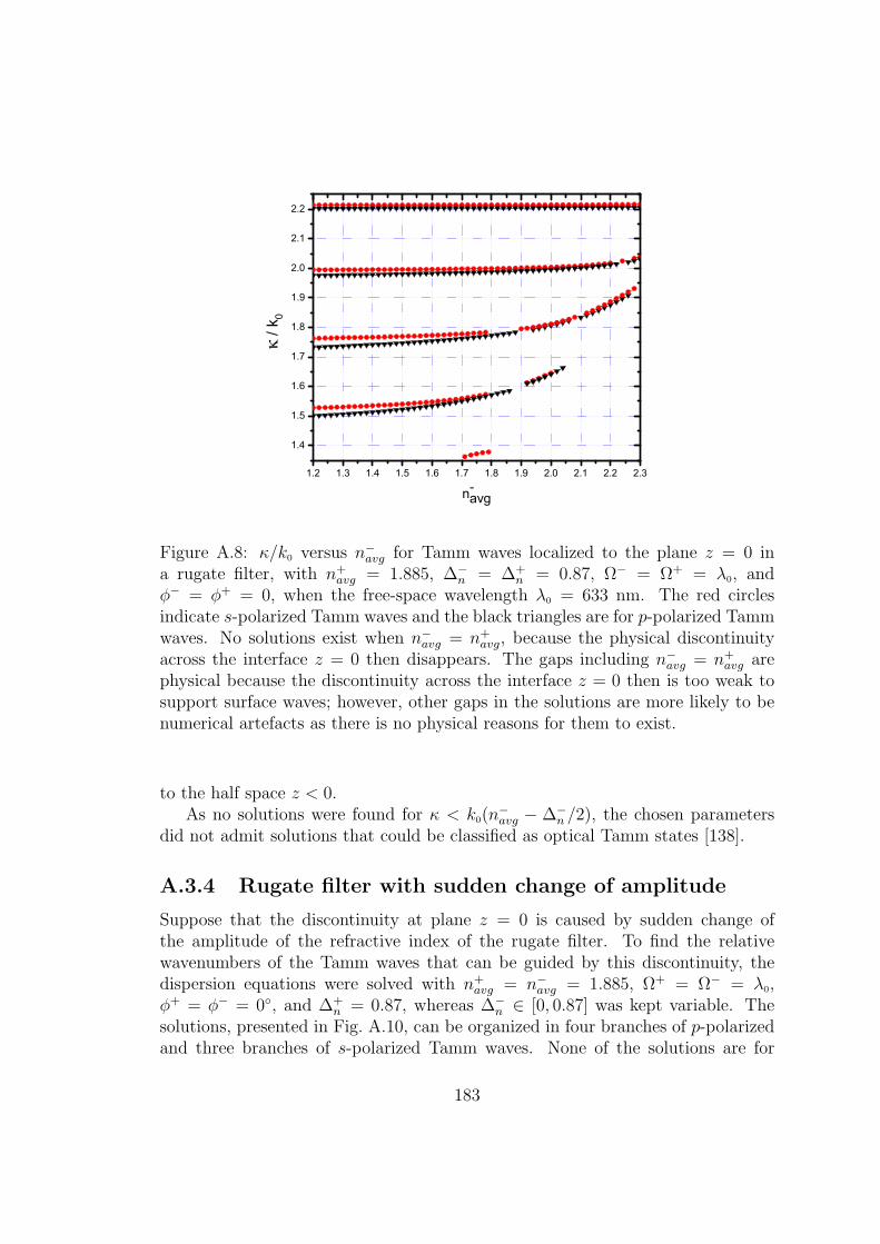
1.2 1.3 1.4 1.5 1.6 1.7 1.8 1.9 2.0 2.1 2.2 2.3
1.4
1.5
1.6
1.7
1.8
1.9
2.0
2.1
2.2
/ k0
n-avg
Figure A.8: κ/k0 versus n−avg for Tamm waves localized to the plane z = 0 in
a rugate filter, with n+avg = 1.885, ∆−
n = ∆+n = 0.87, Ω− = Ω+ = λ0, and
ϕ− = ϕ+ = 0, when the free-space wavelength λ0 = 633 nm. The red circlesindicate s-polarized Tamm waves and the black triangles are for p-polarized Tammwaves. No solutions exist when n−
avg = n+avg, because the physical discontinuity
across the interface z = 0 then disappears. The gaps including n−avg = n+
avg arephysical because the discontinuity across the interface z = 0 then is too weak tosupport surface waves; however, other gaps in the solutions are more likely to benumerical artefacts as there is no physical reasons for them to exist.
to the half space z < 0.As no solutions were found for κ < k0(n
−avg − ∆−
n /2), the chosen parametersdid not admit solutions that could be classified as optical Tamm states [138].
A.3.4 Rugate filter with sudden change of amplitude
Suppose that the discontinuity at plane z = 0 is caused by sudden change ofthe amplitude of the refractive index of the rugate filter. To find the relativewavenumbers of the Tamm waves that can be guided by this discontinuity, thedispersion equations were solved with n+
avg = n−avg = 1.885, Ω+ = Ω− = λ0,
ϕ+ = ϕ− = 0, and ∆+n = 0.87, whereas ∆−
n ∈ [0, 0.87] was kept variable. Thesolutions, presented in Fig. A.10, can be organized in four branches of p-polarizedand three branches of s-polarized Tamm waves. None of the solutions are for
183
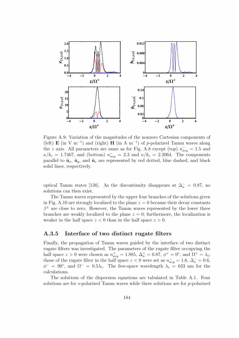
-4 -2 0 2 40.0
0.5
1.0
1.5
2.0
zW+
e 8x,
y,z<
-4 -2 0 2 40
0.004
0.008
0.012
zW+
h 8x,
y,z<
-4 -2 0 2 40
5
10
15
20
zW+
e 8x,
y,z<
-4 -2 0 2 40
0.02
0.06
0.1
0.14
zW+
h 8x,
y,z<
Figure A.9: Variation of the magnitudes of the nonzero Cartesian components of(left) E (in V m−1) and (right) H (in A m−1) of p-polarized Tamm waves alongthe z axis. All parameters are same as for Fig. A.8 except (top) n−
avg = 1.5 andκ/k0 = 1.7467, and (bottom) n−
avg = 2.3 and κ/k0 = 2.2064. The componentsparallel to ux, uy, and uz are represented by red dotted, blue dashed, and blacksolid lines, respectively.
optical Tamm states [138]. As the discontinuity disappears at ∆−n = 0.87, no
solutions can then exist.The Tamm waves represented by the upper four branches of the solutions given
in Fig. A.10 are strongly localized to the plane z = 0 because their decay constantsβ± are close to zero. However, the Tamm waves represented by the lower threebranches are weakly localized to the plane z = 0; furthermore, the localization isweaker in the half space z < 0 than in the half space z > 0.
A.3.5 Interface of two distinct rugate filters
Finally, the propagation of Tamm waves guided by the interface of two distinctrugate filters was investigated. The parameters of the rugate filter occupying thehalf space z > 0 were chosen as n+
avg = 1.885, ∆+n = 0.87, ϕ+ = 0, and Ω+ = λ0;
those of the rugate filter in the half space z < 0 were set as n−avg = 1.6, ∆−
n = 0.6,ϕ− = 90, and Ω− = 0.5λ0. The free-space wavelength λ0 = 633 nm for thecalculations.
The solutions of the dispersion equations are tabulated in Table A.1. Foursolutions are for s-polarized Tamm waves while three solutions are for p-polarized
184

0.0 0.1 0.2 0.3 0.4 0.5 0.6 0.7 0.81.6
1.7
1.8
1.9
2.0
2.1
2.2
2.3
/ k0
-n
Figure A.10: κ/k0 versus ∆−n for Tamm waves localized to the plane z = 0 in a
rugate filter, with n+avg = n−
avg = 1.885, ∆+n = 0.87, Ω− = Ω+ = λ0, ϕ
− = ϕ+ = 0,and ∆−
n ∈ [0, 0.87], when the free-space wavelength λ0 = 633 nm.The red circlesindicate s-polarized Tamm waves and the black triangles are for p-polarized Tammwaves. No solutions can exist when ∆−
n = 0.87.
Table A.1: Relative wavenumber κ/k0 of s-polarized and p-polarized Tamm wavessupported by the interface of two distinct rugate filters, whose parameters areprovided in Section A.3.5. The free-space wavelength λ0 = 633 nm.
s-pol p-pol
2.2147 2.20452.0021 1.99271.8013 1.61011.6178
Tamm waves; no solutions representing optical Tamm states were found. The
185
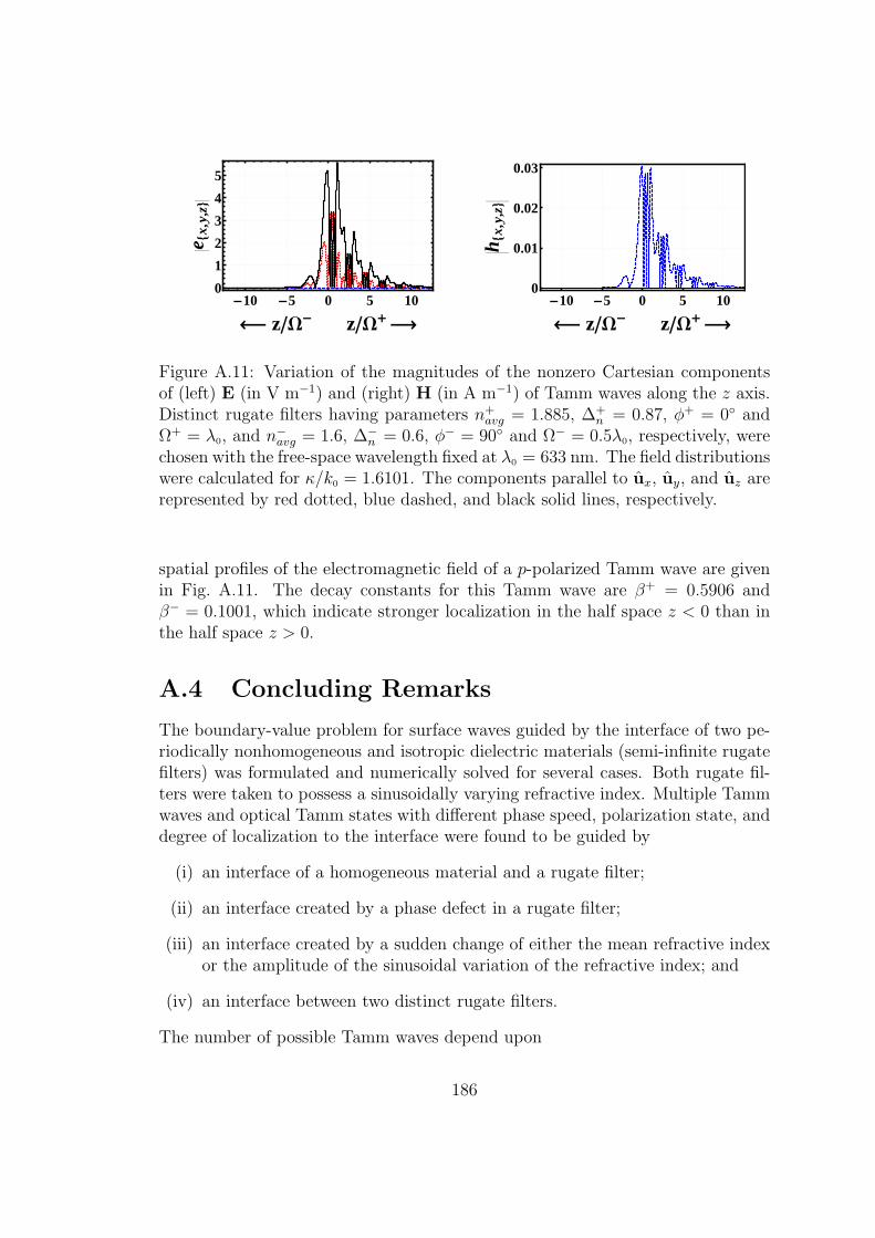
-10 -5 0 5 100
1
2
3
4
5
zW- zW+
e 8x,
y,z<
-10 -5 0 5 100
0.01
0.02
0.03
zW- zW+
h 8x,
y,z<
Figure A.11: Variation of the magnitudes of the nonzero Cartesian componentsof (left) E (in V m−1) and (right) H (in A m−1) of Tamm waves along the z axis.Distinct rugate filters having parameters n+
avg = 1.885, ∆+n = 0.87, ϕ+ = 0 and
Ω+ = λ0, and n−avg = 1.6, ∆−
n = 0.6, ϕ− = 90 and Ω− = 0.5λ0, respectively, werechosen with the free-space wavelength fixed at λ0 = 633 nm. The field distributionswere calculated for κ/k0 = 1.6101. The components parallel to ux, uy, and uz arerepresented by red dotted, blue dashed, and black solid lines, respectively.
spatial profiles of the electromagnetic field of a p-polarized Tamm wave are givenin Fig. A.11. The decay constants for this Tamm wave are β+ = 0.5906 andβ− = 0.1001, which indicate stronger localization in the half space z < 0 than inthe half space z > 0.
A.4 Concluding Remarks
The boundary-value problem for surface waves guided by the interface of two pe-riodically nonhomogeneous and isotropic dielectric materials (semi-infinite rugatefilters) was formulated and numerically solved for several cases. Both rugate fil-ters were taken to possess a sinusoidally varying refractive index. Multiple Tammwaves and optical Tamm states with different phase speed, polarization state, anddegree of localization to the interface were found to be guided by
(i) an interface of a homogeneous material and a rugate filter;
(ii) an interface created by a phase defect in a rugate filter;
(iii) an interface created by a sudden change of either the mean refractive indexor the amplitude of the sinusoidal variation of the refractive index; and
(iv) an interface between two distinct rugate filters.
The number of possible Tamm waves depend upon
186

(i) the refractive index of the homogeneous dielectric partner,
(ii) the amplitude and the period of the sinusoidal nonhomogeneity, and
(iii) the mean refractive index of the rugate filter.
The period of the rugate filter has to be greater than a certain value in order forthe Tamm waves to exist.
While the relative wavenumbers of Tamm waves guided by the interface of ahomogeneous dielectric material and a rugate filter are always greater than therefractive index of the homogeneous material, the phase-defect interface in a rugatefilter was also found to guide surface waves with relative wavenumbers that aresmaller than the minimum refractive index on either side of the phase defect.These surface waves can be classified as optical Tamm states. The Tamm wavescan be either p- or s-polarized, whereas all optical Tamm states were found to bep-polarized.
187

Appendix B
MathematicaTM Codes
B.1 Newton-Raphson Method to Find κ in the
Canonical Boundary-Value Problem of Ch. 2
munot = 4∗ Pi∗ 10ˆ(−7);epsnot = 8.854 10ˆ(−12);lamnot = 633 10ˆ(−9);knot = (2 ∗Pi )/ lamnot ;etanot = Sqrt [ munot/ epsnot ] ;omega = knot/Sqrt [ epsnot ∗ munot ] ;ns = 1.37986 + I ∗7 . 60947 ;epsmet = −56 + I ∗21 ;Cap omega = 200∗ 10ˆ(−9);de l tav = (30∗Pi )/180 ;Chit = (45∗Pi )/180 ;Cap delta = 2∗10ˆ(−9);Ns = 2 Cap omega/Cap delta ;de l tak = 10ˆ(−6);
(∗ Module to c a l c u l a t e determinent o f M∗)
getMdet [ kappa , s t a t e ] :=Module [ kappa = kappa , f l a g 2 = s t a t e ,f l a g = 0 ;While [ f l a g == 0 ,CN = IdentityMatrix [ 4 ] ;For [ n = 1 , n <= 2∗Ns , n++,x1 = 2∗n∗Cap omega/Ns ;x2 = 2∗(n − 1)∗Cap omega/Ns ;
188
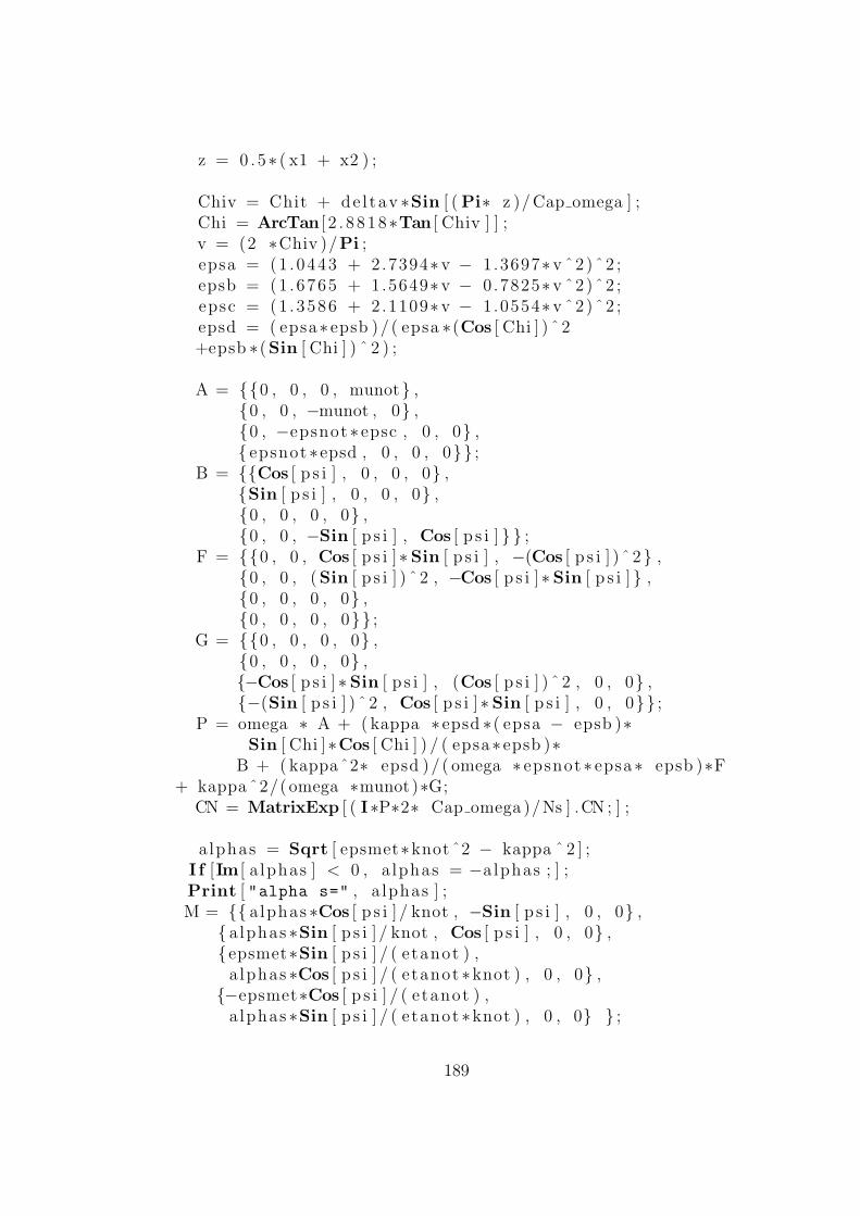
z = 0 .5∗ ( x1 + x2 ) ;
Chiv = Chit + de l tav ∗Sin [ (Pi∗ z )/Cap omega ] ;Chi = ArcTan [ 2 . 8 818∗Tan [ Chiv ] ] ;v = (2 ∗Chiv )/Pi ;epsa = (1 .0443 + 2.7394∗v − 1.3697∗v ˆ2)ˆ2 ;epsb = (1 .6765 + 1.5649∗v − 0.7825∗v ˆ2)ˆ2 ;epsc = (1 .3586 + 2.1109∗v − 1.0554∗v ˆ2)ˆ2 ;epsd = ( epsa∗ epsb )/ ( epsa ∗(Cos [ Chi ] ) ˆ 2+epsb ∗(Sin [ Chi ] ) ˆ 2 ) ;
A = 0 , 0 , 0 , munot ,0 , 0 , −munot , 0 ,0 , −epsnot ∗ epsc , 0 , 0 , epsnot ∗epsd , 0 , 0 , 0 ;
B = Cos [ p s i ] , 0 , 0 , 0 ,Sin [ p s i ] , 0 , 0 , 0 ,0 , 0 , 0 , 0 ,0 , 0 , −Sin [ p s i ] , Cos [ p s i ] ;
F = 0 , 0 , Cos [ p s i ]∗Sin [ p s i ] , −(Cos [ p s i ] ) ˆ 2 ,0 , 0 , (Sin [ p s i ] ) ˆ 2 , −Cos [ p s i ]∗Sin [ p s i ] ,0 , 0 , 0 , 0 ,0 , 0 , 0 , 0 ;
G = 0 , 0 , 0 , 0 ,0 , 0 , 0 , 0 ,−Cos [ p s i ]∗Sin [ p s i ] , (Cos [ p s i ] ) ˆ 2 , 0 , 0 ,−(Sin [ p s i ] ) ˆ 2 , Cos [ p s i ]∗Sin [ p s i ] , 0 , 0 ;
P = omega ∗ A + (kappa ∗ epsd ∗( epsa − epsb )∗Sin [ Chi ]∗Cos [ Chi ] ) / ( epsa∗ epsb )∗
B + ( kappaˆ2∗ epsd )/ ( omega ∗ epsnot ∗ epsa∗ epsb )∗F+ kappa ˆ2/(omega ∗munot)∗G;
CN = MatrixExp [ ( I∗P∗2∗ Cap omega )/Ns ] .CN ; ] ;
a lphas = Sqrt [ epsmet∗knot ˆ2 − kappa ˆ 2 ] ;I f [Im [ a lphas ] < 0 , a lphas = −alphas ; ] ;Print [ "alpha s=" , a lphas ] ;M = alphas ∗Cos [ p s i ] / knot , −Sin [ p s i ] , 0 , 0 ,
alphas ∗Sin [ p s i ] / knot , Cos [ p s i ] , 0 , 0 ,epsmet∗Sin [ p s i ] / ( etanot ) ,a lphas ∗Cos [ p s i ] / ( etanot ∗knot ) , 0 , 0 ,
−epsmet∗Cos [ p s i ] / ( etanot ) ,a lphas ∗Sin [ p s i ] / ( etanot ∗knot ) , 0 , 0 ;
189
eigvalueN , e igvectorN = Eigensystem [CN] ;e igvectorN = Transpose [ e igvectorN ] ;
e igvalueQ = −I∗Log [ e igvalueN ]/ (2∗Cap omega ) ;
n = 3 ;For [m = 1 , m < 5 , m++,I f [Im [ e igvalueQ [ [m] ] ] > 0 ,Print [Im [ e igvalueQ [ [m ] ] ] ] ;M[ [ All , n ] ] = e igvectorN [ [ All , m] ] ; n++];
I f [ n == 5 , m = 5 ; ] ; ] ;
detM = Det [M] ;I f [ detM != 0 , f l a g = 1 ; Break [ ] ; ] ;I f [ detM == 0 && f l a g 2 == 1 ,kappa = −0.0000001∗ knot + kappa ;f l a g = 0 ; ] ;
I f [ detM == 0 && f l a g 2 == 2 ,kappa = 0.0000001∗ knot + kappa ;
f l a g = 0 ; ] ; ] ;detM ]
(∗Newton−Raphson Method ∗)p s i = (0∗Pi )/180 ;y = 1 ;mold = 1 ;t o l = 10ˆ(−14);kappa = N[ ( 2 . 0 6 ) ∗ knot ]While [Abs [Re [ mold ] ] > t o l | | Abs [Im [ mold ] ] > to l ,Print [ S ty l e [ "Iteration No = " , 18 , Red ] , y ] ;y = y + 1 ;kappaold = (1)∗ kappa ;mold = getMdet [ kappaold , 1 ] ;kappanew = (1 + de l tak )∗ kappa ;mol = getMdet [ kappanew , 2 ] ;qold = (mol − mold )/ ( kappanew − kappaold ) ;kappa = kappa − mold/ qold ;Print [ "Det M old=" , mold ] ;Print [ "kappa=" , kappa/knot ] ;I f [ y == 50 , Quit [ ] ; ] ; ]
190

B.2 Plotting the Components of P of a p-Polarized
SPPWave in the Canonical Boundary-Value
Problem of Ch. 2
munot = 4∗ Pi∗ 10ˆ(−7);epsnot = 8.854 10ˆ(−12);lamnot = 633 10ˆ(−9);knot = (2 ∗Pi )/ lamnot ;etanot = Sqrt [ munot/ epsnot ] ;omega = knot/Sqrt [ epsnot ∗ munot ] ;ns = 1.37986 + I ∗7 . 60947 ;epsmet = −56 + I ∗21 ;Cap omega = 200∗ 10ˆ(−9);de l tav = (30∗Pi )/180 ;Chit = (45∗Pi )/180 ;p s i = (0∗Pi )/180 ;kappa = (2 .4550 + I ∗0 .04208)∗ knot ;Cap delta = 2∗10ˆ(−9);Ns = 2 Cap omega/Cap delta ;de l tak = 10ˆ(−6);
(∗ Module to c a l c u l a t e determinent o f M∗)
CN = IdentityMatrix [ 4 ] ;For [ n = 1 , n <= Ns , n++,
x1 = 2∗n∗Cap omega/Ns ;x2 = 2∗(n − 1)∗Cap omega/Ns ;z = 0 .5∗ ( x1 + x2 ) ;Chiv = Chit + de l tav ∗Sin [ (Pi∗ z )/Cap omega ] ;Chi = ArcTan [ 2 . 8818∗Tan [ Chiv ] ] ;v = (2 ∗Chiv )/Pi ;
epsa = (1 .0443 + 2.7394∗v − 1.3697∗v ˆ2)ˆ2 ;epsb = (1 .6765 + 1.5649∗v − 0.7825∗v ˆ2)ˆ2 ;epsc = (1 .3586 + 2.1109∗v − 1.0554∗v ˆ2)ˆ2 ;epsd = ( epsa∗ epsb )/ ( epsa ∗(Cos [ Chi ] ) ˆ 2+ epsb ∗(Sin [ Chi ] ) ˆ 2 ) ;
A = 0 , 0 , 0 , munot ,0 , 0 , −munot , 0 ,0 , −epsnot ∗ epsc , 0 , 0 ,
191

epsnot ∗epsd , 0 , 0 , 0 ;B = Cos [ p s i ] , 0 , 0 , 0 ,
Sin [ p s i ] , 0 , 0 , 0 ,0 , 0 , 0 , 0 ,0 , 0 , −Sin [ p s i ] , Cos [ p s i ] ;
F = 0 , 0 , Cos [ p s i ]∗Sin [ p s i ] , −(Cos [ p s i ] ) ˆ 2 ,0 , 0 , (Sin [ p s i ] ) ˆ 2 , −Cos [ p s i ]∗Sin [ p s i ] ,0 , 0 , 0 , 0 ,0 , 0 , 0 , 0 ;
G = 0 , 0 , 0 , 0 ,0 , 0 , 0 , 0 ,−Cos [ p s i ]∗Sin [ p s i ] , (Cos [ p s i ] ) ˆ 2 , 0 , 0 ,−(Sin [ p s i ] ) ˆ 2 , Cos [ p s i ]∗Sin [ p s i ] , 0 , 0 ;
P = omega ∗ A + (kappa ∗ epsd ∗( epsa − epsb )∗Sin [ Chi ]∗Cos [ Chi ] ) / ( epsa∗ epsb )∗
B + ( kappaˆ2∗ epsd )/ ( omega ∗ epsnot ∗ epsa∗ epsb )∗ F+ kappa ˆ2/(omega ∗munot)∗G;CN = MatrixExp [ ( I∗P∗2∗ Cap omega )/Ns ] .CN ; ] ;
a lphas = Sqrt [ knot ˆ2∗ns ˆ2 − kappa ˆ 2 ] ;I f [Im [ a lphas ] < 0 , a lphas = −alphas ; ] ;
M = alphas ∗Cos [ p s i ] / knot , −Sin [ p s i ] , 0 , 0 , alphas ∗Sin [ p s i ] / knot , Cos [ p s i ] , 0 , 0 ,epsmet∗Sin [ p s i ] / ( etanot ) ,a lphas ∗Cos [ p s i ] / ( etanot ∗knot ) , 0 , 0 ,
−epsmet∗Cos [ p s i ] / ( etanot ) ,a lphas ∗Sin [ p s i ] / ( etanot ∗knot ) , 0 , 0 ;
eigvalueN , e igvectorN = Eigensystem [CN] ;e igvectorN = Transpose [ e igvectorN ] ;
e igvalueQ = −I∗Log [ e igvalueN ]/ (2∗Cap omega ) ;n = 3 ;For [m = 1 , m < 5 , m++,
I f [Im [ e igvalueQ [ [m] ] ] > 0 ,M[ [ All , n ] ] = e igvectorN [ [ All , m] ] ;
n++] ; ] ;detM = Det [M] ;newM = 0 , 0 , 0 , 0 , 0 , 0 , 0 , 0 , 0 ;newM = M[ [ 2 ; ; 4 , 2 ; ; 4 ] ] ;bmat = M[ [ 2 ; ; 4 , 1 ] ] ;
192

Mp = alphas ∗Cos [ p s i ] / knot , −Sin [ p s i ] , alphas ∗Sin [ p s i ] / knot , Cos [ p s i ] ,epsmet∗Sin [ p s i ] / ( etanot ) ,a lphas ∗Cos [ p s i ] / ( etanot ∗knot ) ,
−epsmet∗Cos [ p s i ] / ( etanot ) ,a lphas ∗Sin [ p s i ] / ( etanot ∗knot ) ;
ap = 1 ;as = 0 ;b1 = 0 ;b2 = −M[ [ 1 , 1 ] ] /M[ [ 1 , 3 ] ] ;Print [ "b2 = " , b2 ] ;
fLp = Mp. ap , ase 1 p l i s t = ;e 2 p l i s t = ;e z p l i s t = ;h 1 p l i s t = ;h 2 p l i s t = ;h z p l i s t = ;p 1 p l i s t = p2p l i s t = ;p z p l i s t = ;
CN = IdentityMatrix [ 4 ] ;For [ n = 1 , n <= Ns , n++,
x1 = 2∗n∗Cap omega/Ns ;x2 = 2∗(n − 1)∗Cap omega/Ns ;z = 0 .5∗ ( x1 + x2 ) ;
Chiv = Chit + de l tav ∗Sin [ (Pi∗ z )/Cap omega ] ;Chi = ArcTan [ 2 . 8818∗Tan [ Chiv ] ] ;v = (2 ∗Chiv )/Pi ;
epsa = (1 .0443 + 2.7394∗v − 1.3697∗v ˆ2)ˆ2 ;epsb = (1 .6765 + 1.5649∗v − 0.7825∗v ˆ2)ˆ2 ;epsc = (1 .3586 + 2.1109∗v − 1.0554∗v ˆ2)ˆ2 ;epsd = ( epsa∗ epsb )/ ( epsa ∗(Cos [ Chi ] ) ˆ 2+ epsb ∗(Sin [ Chi ] ) ˆ 2 ) ;
A = 0 , 0 , 0 , munot ,0 , 0 , −munot , 0 ,
193

0 , −epsnot ∗ epsc , 0 , 0 , epsnot ∗epsd , 0 , 0 , 0 ;
B = Cos [ p s i ] , 0 , 0 , 0 ,Sin [ p s i ] , 0 , 0 , 0 ,0 , 0 , 0 , 0 ,0 , 0 , −Sin [ p s i ] , Cos [ p s i ] ;
F = 0 , 0 , Cos [ p s i ]∗Sin [ p s i ] , −(Cos [ p s i ] ) ˆ 2 ,0 , 0 , (Sin [ p s i ] ) ˆ 2 , −Cos [ p s i ]∗Sin [ p s i ] ,0 , 0 , 0 , 0 ,0 , 0 , 0 , 0 ;
G = 0 , 0 , 0 , 0 ,0 , 0 , 0 , 0 ,−Cos [ p s i ]∗Sin [ p s i ] , (Cos [ p s i ] ) ˆ 2 , 0 , 0 ,−(Sin [ p s i ] ) ˆ 2 , Cos [ p s i ]∗Sin [ p s i ] , 0 , 0 ;
P = omega ∗ A +B∗( kappa ∗ epsd ∗( epsa − epsb )∗Sin [ Chi ]∗Cos [ Chi ] ) / ( epsa∗ epsb )
+ ( kappaˆ2∗ epsd )/ ( omega∗ epsnot ∗ epsa∗ epsb )∗ F+ kappa ˆ2/(omega ∗munot)∗G;
exp , eyp , hxp , hyp = CN. fLp ;ezp = ( epsd ∗( epsa − epsb )∗Sin [ Chi ]∗Cos [ Chi ] ) / ( epsa∗ epsb )∗ exp+ ( kappa ∗ epsd )/ ( omega ∗ epsnot ∗ epsa∗ epsb )∗ ( hxp∗Sin [ p s i ]− hyp∗Cos [ p s i ] ) ;hzp = −(kappa /(omega ∗munot ) )∗ ( exp∗Sin [ p s i ] − eyp∗Cos [ p s i ] ) ;hxpc = Conjugate [ hxp ] ;hypc = Conjugate [ hyp ] ;hzpc = Conjugate [ hzp ] ;pxp = Re [ eyp∗hzpc − ezp∗hypc ] / 2 ;pyp = Re [ ezp∗hxpc − exp∗hzpc ] / 2 ;pzp = Re [ exp∗hypc − eyp∗hxpc ] / 2 ;
e1p = exp∗Cos [ p s i ] + eyp∗Sin [ p s i ] ;e2p = −exp∗Sin [ p s i ] + eyp∗Cos [ p s i ] ;h1p = hxp∗Cos [ p s i ] + hyp∗Sin [ p s i ] ;h2p = −hxp∗Sin [ p s i ] + hyp∗Cos [ p s i ] ;p1p = pxp∗Cos [ p s i ] + pyp∗Sin [ p s i ] ;p2p = −pxp∗Sin [ p s i ] + pyp∗Cos [ p s i ] ;
e 1 p l i s t = Append [ e 1 p l i s t , ( z )/Cap omega ,Abs [ exp∗Cos [ p s i ] + eyp∗Sin [ p s i ] ] ] ;
e 2 p l i s t = Append [ e 2 p l i s t , ( z )/Cap omega ,Abs[−exp∗Sin [ p s i ] + eyp∗Cos [ p s i ] ] ] ;
194

e z p l i s t = Append [ e z p l i s t , ( z )/Cap omega , Abs [ ezp ] ] ;h 1 p l i s t = Append [ h 1p l i s t , ( z )/Cap omega ,
Abs [ hxp∗Cos [ p s i ] + hyp∗Sin [ p s i ] ] ] ;h 2 p l i s t = Append [ h 2p l i s t , ( z )/Cap omega ,
Abs[−hxp∗Sin [ p s i ] + hyp∗Cos [ p s i ] ] ] ;h z p l i s t = Append [ h zp l i s t , ( z )/Cap omega , Abs [ hzp ] ] ;p 1 p l i s t = Append [ p 1p l i s t ,
( z )/Cap omega , pxp∗Cos [ p s i ] + pyp∗Sin [ p s i ] ] ;p 2 p l i s t = Append [ p 2p l i s t , ( z )/Cap omega , −pxp∗Sin [ p s i ]+ pyp∗Cos [ p s i ] ] ;p z p l i s t = Append [ p zp l i s t , ( z )/Cap omega , pzp ] ;
CN = MatrixExp [ ( I∗P∗2∗ Cap omega )/Ns ] .CN ; ] ;
e 1ml i s t = ;e 2ml i s t = ;e zm l i s t = ;h1ml i s t = ;h2ml i s t = ;hzml i s t = ;p1ml i s t = p2ml i s t = ;pzml i s t = ;For [ z = 0∗Cap omega , z >= −0.41∗Cap omega ,z = z − 0 .01∗Cap omega ,exm = (ap∗ alphas ∗Cos [ p s i ] / knot − as∗Sin [ p s i ] ) ∗Exp[−I∗ alphas ∗z ] ;eym = (ap∗ alphas ∗Sin [ p s i ] / knot + as∗Cos [ p s i ] ) ∗Exp[−I∗ alphas ∗z ] ;ezm = ap∗kappa∗Exp[−I∗ alphas ∗z ] / knot ;hxm = ( as∗ alphas ∗Cos [ p s i ] / knot + ap∗epsmet∗Sin [ p s i ] ) ∗
Exp[−I∗ alphas ∗z ] / ( etanot ) ;hym = ( as∗ alphas ∗Sin [ p s i ] / knot − ap∗epsmet∗Cos [ p s i ] ) ∗
Exp[−I∗ alphas ∗z ] / ( etanot ) ;hzm = as∗kappa∗Exp[−I∗ alphas ∗z ] / ( knot∗ etanot ) ;
hxmc = Conjugate [ hxm ] ;hymc = Conjugate [ hym ] ;hzmc = Conjugate [ hzm ] ;pxm = Re [ eym∗hzmc − ezm∗hymc ] / 2 ;pym = Re [ ezm∗hxmc − exm∗hzmc ] / 2 ;pzm = Re [ exm∗hymc − eym∗hxmc ] / 2 ;
e1m = exm∗Cos [ p s i ] + eym∗Sin [ p s i ] ;
195

e2m = −exm∗Sin [ p s i ] + eym∗Cos [ p s i ] ;h1m = hxm∗Cos [ p s i ] + hym∗Sin [ p s i ] ;h2m = −hxm∗Sin [ p s i ] + hym∗Cos [ p s i ] ;p1m = pxm∗Cos [ p s i ] + pym∗Sin [ p s i ] ;p2m = −pxm∗Sin [ p s i ] + pym∗Cos [ p s i ] ;
e 1ml i s t = Append [ e1ml i s t , ( z )/Cap omega ,Abs [ exm∗Cos [ p s i ] + eym∗Sin [ p s i ] ] ] ;
e 2ml i s t = Append [ e2ml i s t , ( z )/Cap omega ,Abs[−exm∗Sin [ p s i ] + eym∗Cos [ p s i ] ] ] ;
e zm l i s t = Append [ e zml i s t , ( z )/Cap omega , Abs [ ezm ] ] ;h1ml i s t = Append [ h1mlist , ( z )/Cap omega ,
Abs [ hxm∗Cos [ p s i ] + hym∗Sin [ p s i ] ] ] ;h2ml i s t = Append [ h2mlist , ( z )/Cap omega ,
Abs[−hxm∗Sin [ p s i ] + hym∗Cos [ p s i ] ] ] ;hzml i s t = Append [ hzml i st , ( z )/Cap omega , Abs [ hzm ] ] ;p1ml i s t = Append [ p1mlist ,( z )/Cap omega , pxm∗Cos [ p s i ] + pym∗Sin [ p s i ] ] ;
p2ml i s t = Append [ p2mlist ,( z )/Cap omega , −pxm∗Sin [ p s i ] + pym∗Cos [ p s i ] ] ;
pzml i s t = Append [ pzml i st , ( z )/Cap omega , pzm ] ; ]
ep = L i s tL ineP lo t [ e 1p l i s t , e 2 p l i s t , e z p l i s t ] ;hp = Li s tL ineP lo t [ h1p l i s t , h2p l i s t , h z p l i s t ] ;pp = Li s tL ineP lo t [ p1p l i s t , p2p l i s t , p z p l i s t ] ;
em = Li s tL ineP lo t [ e1ml i s t , e2ml i s t , e zm l i s t ] ;hm = Li s tL ineP lo t [ h1mlist , h2mlist , hzml i s t ] ;pm = Li s tL ineP lo t [ p1mlist , p2mlist , pzml i s t ] ;g = Grid [em, ep , hm, hp , pm, pp , Spac ings −> 0 , 0 ]
B.3 Newton-Raphson Method to Find κ in the
Canonical Boundary-Value Problem of Ch. 5
munot = 4∗ Pi∗ 10ˆ(−7);epsnot = 8.854 10ˆ(−12);lamnot = 633 10ˆ(−9);knot = (2 ∗Pi )/ lamnot ;etanot = Sqrt [ munot/ epsnot ] ;omega = knot/Sqrt [ epsnot ∗ munot ] ;ns = 1.37986 + I ∗7 . 60947 ;epsmet = −56 + I ∗21 ;
196
Cap omega = 200∗ 10ˆ(−9);de l tav = (30∗Pi )/180 ;Chit = (45∗Pi )/180 ;Cap delta = 2∗10ˆ(−9);Ns = 2 Cap omega/Cap delta ;de l tak = 10ˆ(−6);
(∗ Module to c a l c u l a t e determinent o f M∗)
getMdet [ kappa , s t a t e ] :=Module [ kappa = kappa , f l a g 2 = s t a t e ,f l a g = 0 ;While [ f l a g == 0 ,CNp = IdentityMatrix [ 4 ] ;CNn = IdentityMatrix [ 4 ] ;For [ n = 1 , n <= Ns , n++,x1 = 2∗n∗Cap omega/Ns ;x2 = 2∗(n − 1)∗Cap omega/Ns ;z = 0 .5∗ ( x1 + x2 ) ;
Chivp = Chit + de l tav ∗Sin [ (Pi∗ ( z ) )/ Cap omega ] ;Chivn = Chit − de l tav ∗Sin [ (Pi∗ (−z ) )/ Cap omega ] ;Chip = ArcTan [ 2 . 8818∗Tan [ Chivp ] ] ;Chin = ArcTan [ 2 . 8818∗Tan [ Chivn ] ] ;vp = (2 ∗Chivp )/Pi ;vn = (2 ∗Chivn )/Pi ;
epsap = (1 .0443 + 2.7394∗vp − 1.3697∗vp ˆ2)ˆ2 ;epsbp = (1 .6765 + 1.5649∗vp − 0.7825∗vp ˆ2)ˆ2 ;epscp = (1 .3586 + 2.1109∗vp − 1.0554∗vp ˆ2)ˆ2 ;epsdp = ( epsap∗epsbp )/ ( epsap ∗(Cos [ Chip ] ) ˆ 2+ epsbp ∗(Sin [ Chip ] ) ˆ 2 ) ;
epsan = (1 .0443 + 2.7394∗vn − 1.3697∗vn ˆ2)ˆ2 ;epsbn = (1 .6765 + 1.5649∗vn − 0.7825∗vn ˆ2)ˆ2 ;epscn = (1 .3586 + 2.1109∗vn − 1.0554∗vn ˆ2)ˆ2 ;epsdn = ( epsan∗epsbn )/ ( epsan ∗(Cos [ Chin ] ) ˆ 2+ epsbn ∗(Sin [ Chin ] ) ˆ 2 ) ;
Ap = 0 , 0 , 0 , munot ,0 , 0 , −munot , 0 , epsnot ∗( epscp − epsdp )∗Cos [ gammap]∗
197

Sin [ gammap ] , −epsnot ∗( epscp ∗(Cos [ gammap] ) ˆ 2+ epsdp ∗(Sin [ gammap ] ) ˆ 2 ) , 0 , 0 ,
epsnot ∗( epscp ∗(Sin [ gammap] ) ˆ 2 + epsdp ∗(Cos [ gammap ] ) ˆ 2 ) ,−epsnot ∗( epscp − epsdp )∗Cos [ gammap ] ∗Sin [ gammap ] , 0 , 0 ;
Bp = Cos [ gammap ] , Sin [ gammap ] , 0 , 0 ,0 , 0 , 0 , 0 ,0 , 0 , 0 , −Sin [ gammap] ,0 , 0 , 0 , Cos [ gammap ] ;
Fp = 0 , 0 ,0 , −((kappaˆ2∗ epsdp )/( omega ∗ epsnot ∗ epsap∗ epsbp ) ) ,
0 , 0 , 0 , 0 ,0 , kappa ˆ2/(omega ∗munot ) , 0 , 0 ,0 , 0 , 0 , 0 ;
Pp = omega ∗ Ap + ( kappa ∗epsdp ∗( epsap − epsbp )∗Sin [ Chip ]∗Cos [ Chip ] ) / ( epsap∗epsbp )∗Bp + Fp ;
An = 0 , 0 , 0 , munot ,0 , 0 , −munot , 0 , epsnot ∗( epscn − epsdn )∗Cos [ gamman]∗ Sin [ gamman ] ,−epsnot ∗( epscn ∗(Cos [ gamman] ) ˆ 2 + epsdn ∗(Sin [ gamman ] ) ˆ 2 ) ,0 , 0 , epsnot ∗( epscn ∗(Sin [ gamman] ) ˆ 2 + epsdn ∗(Cos [ gamman ] ) ˆ 2 ) ,
−epsnot ∗( epscn − epsdn )∗Cos [ gamman ] ∗Sin [ gamman ] , 0 , 0 ;Bn = Cos [ gamman ] , Sin [ gamman ] , 0 , 0 ,
0 , 0 , 0 , 0 ,0 , 0 , 0 , −Sin [ gamman] ,0 , 0 , 0 , Cos [ gamman ] ;
Fn = 0 , 0 , 0 ,−((kappaˆ2∗ epsdn )/ ( omega ∗ epsnot ∗ epsan∗ epsbn ) ) ,
0 , 0 , 0 , 0 , 0 , kappa ˆ2/(omega ∗munot ) , 0 , 0 ,0 , 0 , 0 , 0 ;
Pn = omega ∗ An + ( kappa ∗epsdn ∗( epsan − epsbn )∗Sin [ Chin ]∗Cos [ Chin ] ) / ( epsan∗epsbn )∗Bn + Fn ;
CNp = MatrixExp [ ( I∗Pp∗2∗ Cap omega )/Ns ] .CNp;CNn = MatrixExp[−(( I∗Pn∗2∗ Cap omega )/Ns ) ] .CNn ; ] ;
Mp = 0 , 0 ,0 , 0 ,0 , 0 ,0 , 0 ;Mn = 0 , 0 ,0 , 0 ,0 , 0 ,0 , 0 ;
eigvalueNp , e igvectorNp = Eigensystem [CNp ] ;e igvectorNp = Transpose [ e igvectorNp ] ;
198

eigvalueNn , e igvectorNn = Eigensystem [CNn ] ;e igvectorNn = Transpose [ e igvectorNn ] ;
e igvalueQp = −I∗Log [ e igvalueNp ]/ (2∗Cap omega ) ;e igvalueQn = I∗Log [ e igvalueNn ]/ (2∗Cap omega ) ;
n = 1 ;For [m = 1 , m < 5 , m++,I f [Im [ e igvalueQp [ [m] ] ] > 0 ,Mp[ [ All , n ] ] = eigvectorNp [ [ All , m] ] ;n++] ; ] ;
n = 1 ;For [m = 1 , m < 5 , m++,I f [Im [ e igvalueQn [ [m] ] ] < 0 ,Mn[ [ All , n ] ] = eigvectorNn [ [ All , m] ] ;n++] ; ] ;
M = Transpose [ Join [Transpose [Mp] , Transpose [Mn ] ] ] ;detM = Det [M] ;I f [ detM != 0 , f l a g = 1 ; Break [ ] ; ] ;I f [ detM == 0 && f l a g 2 == 1 ,kappa = −0.0000001∗ knot + kappa ;f l a g = 0 ; ] ;
I f [ detM == 0 && f l a g 2 == 2 ,kappa = 0.0000001∗ knot + kappa ;f l a g = 0 ; ] ; ] ;
detM ]
(∗Newton−Raphson Method ∗)gammap = (0∗Pi )/180 ;gamman = (90∗Pi )/180 ;y = 1 ;mold = 1 ;t o l = 10ˆ(−14);kappa = N[ ( 2 . 0 4 ) ∗ knot ]While [Abs [ mold ] > to l ,Print [ S ty l e [ "Iteration No = " , 18 , Red ] , y ] ;y = y + 1 ;kappaold = (1)∗ kappa ;mold = getMdet [ kappaold , 1 ] ;kappanew = (1 + de l tak )∗ kappa ;
mol = getMdet [ kappanew , 2 ] ;
199
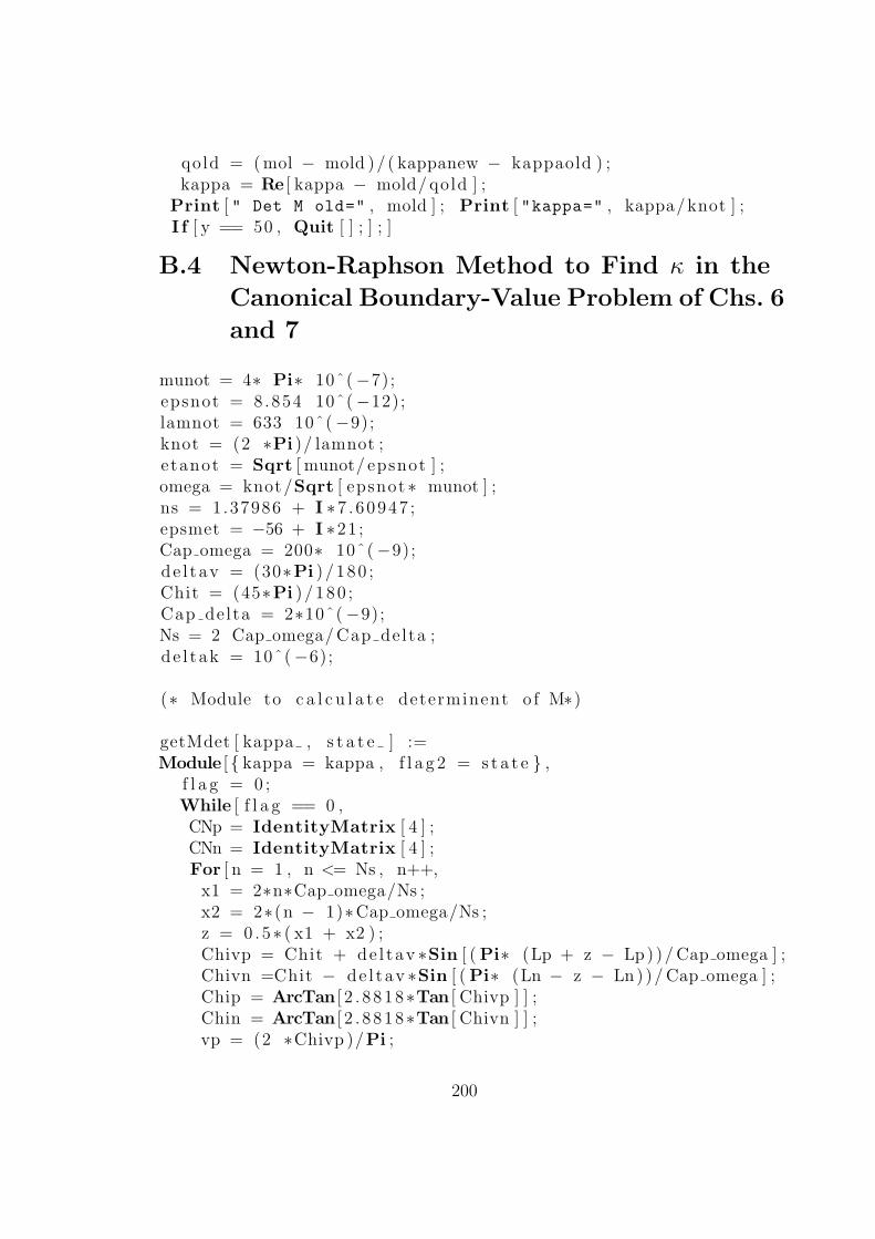
qold = (mol − mold )/ ( kappanew − kappaold ) ;kappa = Re [ kappa − mold/ qold ] ;
Print [ " Det M old=" , mold ] ; Print [ "kappa=" , kappa/knot ] ;I f [ y == 50 , Quit [ ] ; ] ; ]
B.4 Newton-Raphson Method to Find κ in the
Canonical Boundary-Value Problem of Chs. 6
and 7
munot = 4∗ Pi∗ 10ˆ(−7);epsnot = 8.854 10ˆ(−12);lamnot = 633 10ˆ(−9);knot = (2 ∗Pi )/ lamnot ;etanot = Sqrt [ munot/ epsnot ] ;omega = knot/Sqrt [ epsnot ∗ munot ] ;ns = 1.37986 + I ∗7 . 60947 ;epsmet = −56 + I ∗21 ;Cap omega = 200∗ 10ˆ(−9);de l tav = (30∗Pi )/180 ;Chit = (45∗Pi )/180 ;Cap delta = 2∗10ˆ(−9);Ns = 2 Cap omega/Cap delta ;de l tak = 10ˆ(−6);
(∗ Module to c a l c u l a t e determinent o f M∗)
getMdet [ kappa , s t a t e ] :=Module [ kappa = kappa , f l a g 2 = s t a t e ,
f l a g = 0 ;While [ f l a g == 0 ,CNp = IdentityMatrix [ 4 ] ;CNn = IdentityMatrix [ 4 ] ;For [ n = 1 , n <= Ns , n++,x1 = 2∗n∗Cap omega/Ns ;x2 = 2∗(n − 1)∗Cap omega/Ns ;z = 0 .5∗ ( x1 + x2 ) ;Chivp = Chit + de l tav ∗Sin [ (Pi∗ (Lp + z − Lp))/Cap omega ] ;Chivn =Chit − de l tav ∗Sin [ (Pi∗ (Ln − z − Ln))/Cap omega ] ;Chip = ArcTan [ 2 . 8818∗Tan [ Chivp ] ] ;Chin = ArcTan [ 2 . 8818∗Tan [ Chivn ] ] ;vp = (2 ∗Chivp )/Pi ;
200

vn = (2 ∗Chivn )/Pi ;
epsap = (1 .0443 + 2.7394∗vp − 1.3697∗vp ˆ2)ˆ2 ;epsbp = (1 .6765 + 1.5649∗vp − 0.7825∗vp ˆ2)ˆ2 ;epscp = (1 .3586 + 2.1109∗vp − 1.0554∗vp ˆ2)ˆ2 ;epsdp = ( epsap∗epsbp )/ ( epsap ∗(Cos [ Chip ] ) ˆ 2+ epsbp ∗(Sin [ Chip ] ) ˆ 2 ) ;
epsan = (1 .0443 + 2.7394∗vn − 1.3697∗vn ˆ2)ˆ2 ;epsbn = (1 .6765 + 1.5649∗vn − 0.7825∗vn ˆ2)ˆ2 ;epscn = (1 .3586 + 2.1109∗vn − 1.0554∗vn ˆ2)ˆ2 ;epsdn = ( epsan∗epsbn )/ ( epsan ∗(Cos [ Chin ] ) ˆ 2+ epsbn ∗(Sin [ Chin ] ) ˆ 2 ) ;
Ap = 0 , 0 , 0 , munot ,0 , 0 , −munot , 0 , epsnot ∗( epscp − epsdp )∗Cos [ gammap]∗ Sin [ gammap ] ,−epsnot ∗( epscp ∗(Cos [ gammap] ) ˆ 2
+ epsdp ∗(Sin [ gammap ] ) ˆ 2 ) , 0 , 0 , epsnot ∗( epscp ∗(Sin [ gammap] ) ˆ 2
+ epsdp ∗(Cos [ gammap ] ) ˆ 2 ) ,−epsnot ∗( epscp − epsdp )∗Cos [ gammap ] ∗Sin [ gammap ] ,0 , 0 ;Bp = Cos [ gammap ] , Sin [ gammap ] , 0 , 0 ,
0 , 0 , 0 , 0 , 0 , 0 , 0 , −Sin [ gammap] ,0 , 0 , 0 , Cos [ gammap] ;
Fp = 0 , 0 , 0 ,−((kappaˆ2∗ epsdp )/( omega ∗ epsnot ∗ epsap∗ epsbp ) ) ,
0 , 0 , 0 , 0 , 0 , kappa ˆ2/(omega ∗munot ) , 0 , 0 ,0 , 0 , 0 , 0 ;
Pp = omega ∗ Ap + ( kappa ∗epsdp ∗( epsap − epsbp )∗Sin [ Chip ]∗Cos [ Chip ] ) / ( epsap∗epsbp )∗Bp + Fp ;
An = 0 , 0 , 0 , munot , 0 , 0 , −munot , 0 , epsnot ∗( epscn − epsdn )∗Cos [ gamman]∗Sin [ gamman ] ,−epsnot ∗( epscn ∗(Cos [ gamman] ) ˆ 2
+ epsdn ∗(Sin [ gamman] ) ˆ 2 ) , 0 , 0 , epsnot ∗( epscn ∗(Sin [ gamman] ) ˆ 2 + epsdn ∗(Cos [ gamman ] ) ˆ 2 ) ,
−epsnot ∗( epscn − epsdn )∗Cos [ gamman ] ∗Sin [ gamman ] , 0 , 0 ;Bn = Cos [ gamman ] , Sin [ gamman ] , 0 , 0 ,
0 , 0 , 0 , 0 , 0 , 0 , 0 , −Sin [ gamman] ,0 , 0 , 0 , Cos [ gamman ] ;
201

Fn = 0 , 0 , 0 ,−((kappaˆ2∗ epsdn )/( omega ∗ epsnot ∗ epsan∗ epsbn ) ) ,
0 , 0 , 0 , 0 , 0 , kappa ˆ2/(omega ∗munot ) , 0 , 0 ,0 , 0 , 0 , 0 ;
Pn = omega ∗ An + ( kappa ∗epsdn ∗( epsan − epsbn )∗Sin [ Chin ]∗Cos [ Chin ] ) / ( epsan∗epsbn )∗Bn + Fn ;
CNp = MatrixExp [ ( I∗Pp∗2∗ Cap omega )/Ns ] .CNp;CNn = MatrixExp[−(( I∗Pn∗2∗ Cap omega )/Ns ) ] .CNn ; ] ;
Amet = 0 , 0 , 0 , munot , 0 , 0 , −munot , 0 ,0 , −epsnot ∗epsmet , 0 , 0 , epsnot ∗epsmet , 0 , 0 , 0 ;
Bmet = 0 , 0 , 0 , −(kappa ˆ2/(omega ∗ epsnot ∗epsmet ) ) ,0 , 0 , 0 , 0 ,0 , kappa ˆ2/(omega ∗munot ) , 0 , 0 ,0 , 0 , 0 , 0 ;
Pmet = omega ∗Amet + Bmet ;
Mp = 0 , 0 ,0 , 0 ,0 , 0 ,0 , 0 ;Mn =0 , 0 ,0 , 0 ,0 , 0 ,0 , 0 ;
eigvalueNp , e igvectorNp = Eigensystem [CNp ] ;e igvectorNp = Transpose [ e igvectorNp ] ;
eigvalueNn , e igvectorNn = Eigensystem [CNn ] ;e igvectorNn = Transpose [ e igvectorNn ] ;
e igvalueQp = −I∗Log [ e igvalueNp ]/ (2∗Cap omega ) ;e igvalueQn = I∗Log [ e igvalueNn ]/ (2∗Cap omega ) ;
n = 1 ;For [m = 1 , m < 5 , m++,I f [Im [ e igvalueQp [ [m] ] ] > 0 ,Mp[ [ All , n ] ] = eigvectorNp [ [ All , m] ] ;n++] ; ] ;
n = 1 ;For [m = 1 , m < 5 , m++,I f [Im [ e igvalueQn [ [m] ] ] < 0 ,Mn[ [ All , n ] ] = eigvectorNn [ [ All , m] ] ;n++] ; ] ;
M = Transpose [ Join [Transpose [Mp] ,Transpose [MatrixExp [ I∗Pmet∗(Lp − Ln ) ] .Mn ] ] ] ;
202

detM = Det [M] ;I f [ detM != 0 , f l a g = 1 ; Break [ ] ; ] ;I f [ detM == 0 && f l a g 2 == 1 ,
kappa = −0.0000001∗ knot + kappa ;f l a g = 0 ; ] ;
I f [ detM == 0 && f l a g 2 == 2 ,kappa = 0.0000001∗ knot + kappa ;f l a g = 0 ; ] ; ] ;
detM ]
(∗ Newton−Raphson Method ∗)gammap = (0∗Pi )/180 ;gamman = (0∗Pi )/180 ;Lp = 7.5∗10ˆ(−9) ;Ln = −7.5∗10ˆ(−9);y = 1 ;mold = 1 ;t o l = 10ˆ(−14);kappa = N[ ( 1 . 8 7 ) ∗ knot ]While [Abs [Re [ mold ] ] > t o l | | Abs [Im [ mold ] ] > to l ,Print [ S ty l e [ "Iteration No = " , 18 , Red ] , y ] ;y = y + 1 ;kappaold = (1)∗ kappa ;mold = getMdet [ kappaold , 1 ] ;kappanew = (1 + de l tak )∗ kappa ;
mol = getMdet [ kappanew , 2 ] ;qold = (mol − mold )/ ( kappanew − kappaold ) ;kappa = kappa − mold/ qold ;
Print [ " Det M old=" , mold ] ; Print [ "kappa=" , kappa/knot ] ;I f [ y == 50 , Quit [ ] ; ] ; ]
B.5 Ap vs. θ in the TKR Configuration of Ch. 8
munot = 4∗ Pi∗ 10ˆ(−7);epsnot = 8.854 ∗10ˆ(−12);lamnot = 633∗10ˆ(−9);knot = N[ ( 2 ∗Pi )/ lamnot ] ;e tanot = Sqrt [ munot/ epsnot ] ;omega = knot/Sqrt [ epsnot ∗ munot ] ;nss = 0 .75 + I ∗ 3 . 9 ;epm = nss ˆ2 ;
203

nl = 2 . 5 8 ;na = 1 . 4 5 ;nb = 2 . 3 2 ;NA = (na + nb)/2NB = (nb − na ) / 2 ;Np = 3 ;HP = 1.5∗ lamnot ;Ld = 2∗HP∗Np;Ns = 2∗HP/(2∗10ˆ(−9)) ;Print [ Ns ] ;Ns = 950 ;tn = 30 ;tm = 65 ;Lm = 30∗10ˆ(−9);
a p l i s t = ;For [NN = tn , NN < tm , NN = NN + 0.01 ,theta = NN∗Pi /180 ;kappa = knot∗ nl ∗Sin [ theta ] ;
Z [ Ns + 1 ] = −Cos [ theta ] , −nl / etanot ;
For [ n = Ns + 1 , n >= 2 , n−−,x1 = Lm + (Ld)∗ ( n − 1)/Ns ;x2 = Lm + (Ld)∗ ( n − 2)/Ns ;z = 0 .5∗ ( x1 + x2 ) ;epd = (NA + NB∗Sin [Pi ( z − Lm)/HP] ) ˆ 2 ;Pd = 0 , omega∗munot − kappa ˆ2/(omega∗ epsnot ∗epd ) ,omega∗ epsnot ∗epd , 0 ;
DN1, GN11 = Eigensystem [ Pd ] ;GN1 = Transpose [GN11 ] ;I f [Im [DN1 [ [ 1 ] ] ] < Im [DN1 [ [ 2 ] ] ] ,a1 = DN1 [ [ 1 ] ] ;b1 = GN1 [ [ All , 1 ] ] ;DN1 [ [ 1 ] ] = DN1 [ [ 2 ] ] ;DN1 [ [ 2 ] ] = a1 ;GN1 [ [ All , 1 ] ] = GN1 [ [ All , 2 ] ] ;GN1 [ [ All , 2 ] ] = b1 ; ] ;
W = Inverse [GN1 ] . Z [ n ] ;WU[ n ] = W[ [ 1 , 1 ] ] ;WL[ n ] = W[ [ 2 , 1 ] ] ;DM = DiagonalMatrix [DN1 ] ;
204

DU[ n ] = DM[ [ 1 , 1 ] ] ;DL[ n ] = DM[ [ 2 , 2 ] ] ;Lower1 =Exp[−I∗Ld∗DL[ n ] /Ns ]∗WL[ n ]∗Exp [ I∗Ld∗DU[ n ] /Ns ] /WU[ n ] ;Dummy1 = 1 , Lower1 ;Z [ n − 1 ] = GN1.Dummy1 ; ] ;
Pm = 0 , omega∗munot − kappa ˆ2/(omega∗ epsnot ∗epm) ,omega∗ epsnot ∗epm , 0 ;
DN3, GN33 = Eigensystem [Pm] ;GN3 = Transpose [GN33 ] ;
I f [Im [DN3 [ [ 1 ] ] ] < Im [DN3 [ [ 2 ] ] ] ,a3 = DN3 [ [ 1 ] ] ;b3 = GN3 [ [ All , 1 ] ] ;DN3 [ [ 1 ] ] = DN3 [ [ 2 ] ] ;DN3 [ [ 2 ] ] = a3 ;GN3 [ [ All , 1 ] ] = GN3 [ [ All , 2 ] ] ;GN3 [ [ All , 2 ] ] = b3 ; ] ;
W = Inverse [GN3 ] . Z [ 1 ] ;WU[ 1 ] = W[ [ 1 , 1 ] ] ;WL[ 1 ] = W[ [ 2 , 1 ] ] ;DM = DiagonalMatrix [DN3 ] ;DU[ 1 ] = DM[ [ 1 , 1 ] ] ;DL[ 1 ] = DM[ [ 2 , 2 ] ] ;Lower2 = Exp[−I∗Lm∗DL[ 1 ] ] ∗WL[ 1 ] ∗Exp [ I∗Lm∗DU[ 1 ] ] /WU[ 1 ] ;Dummy2 = 1 , Lower2 ;Z [ 0 ] = GN3.Dummy2;
dummy60 = Z [ 0 ] [ [ 1 , 1 ] ] , −Cos [ theta ] ,Z [ 0 ] [ [ 2 , 1 ] ] , n l / etanot ;
T0RP = Inverse [ dummy60].−Cos [ theta ] , −nl / etanot ;T0P = T0RP[ [ 1 , 1 ] ] ;RP = T0RP[ [ 2 , 1 ] ] ;TP[ 0 ] = T0P;TP[ 1 ] = Exp [ I∗Lm∗DU[ 1 ] ] ∗TP[ 0 ] /WU[ 1 ] ;
Clear [ i ] ;For [ i = 2 , i <= Ns + 1 , i++,TP[ i ] = Exp [ I∗Ld∗DU[ i ] /Ns ]∗TP[ i − 1 ]/WU[ i ] ; ] ;rpp = Abs [RP] ˆ 2 ;PAB = 1 − Abs [TP[ Ns + 1 ] ] ˆ 2 − Abs [RP] ˆ 2 ;
205
a p l i s t = Append [ a p l i s t , NN, PAB ] ; ]
Needs [ "PlotLegends ‘" ] ;applot = L i s tL ineP lo t [ a p l i s t ]a p l i s t // MatrixForm
B.6 Ap vs. θ in the Grating-Coupled Configura-
tion of Chs. 9 and 10
munot = 4∗ Pi∗ 10ˆ(−7);epsnot = 8.854 10ˆ(−12);lamnot = 633 10ˆ(−9);knot = N[ ( 2 ∗Pi )/ lamnot ] ;e tanot = Sqrt [ munot/ epsnot ] ;omega = knot/Sqrt [ epsnot ∗ munot ] ;nss = 1.37986 + I ∗7 . 6097 ;epm = nss ˆ2 ;L = lamnot ;d1 = 4∗ lamnot ;d2 = d1 + 50∗10ˆ(−9);d3 = d2 + 30∗10ˆ(−9);L1 = 0 .5 L ;na = 1 . 4 5 ;nb = 2 . 3 2 ;NA = (na + nb)/2NB = (nb − na ) / 2 ;HP = lamnot ;a p l i s t = ;
Nt = 8 ;Nd = d1 /2 ;Ng = 50 ;Ns = Nd + Ng ;(∗ begin Module ep s i l o n ( z , n ) ∗)epzn [ zz , nn ] := Module [ z = zz , n = nn , y , A, B, CD ,
A = epm + epd ;B = epm − epd ;CD = d2 − d1 ;y = L1∗ArcSin [ ( d2 − z )/CD]/Pi ;epd = (NA + NB∗Sin [Pi ( d2 − z )/HP] ) ˆ 2 ;I f [ n == 0 ,I f [ z <= d1 ,
206

ep s i l o n = epd ; ] ;I f [ z > d1 && z < d2 ,e p s i l o n = ( epd ∗(L − L1 + 2∗y ) + epm∗(L1 − 2∗y ) )/L ; ] ;
I f [ z >= d2 ,e p s i l o n = epm ; ] ;
] ;
I f [ n != 0 ,I f [ z <= d1 ,e p s i l o n = 0 ; ] ;
I f [ z > d1 && z < d2 ,e p s i l o n = (B∗Exp[−I∗n∗(L1 − y)∗2∗Pi/L ]
− B∗Exp[−I∗n∗y∗2∗Pi/L ] ) ∗I /(n∗2∗Pi ) ; ] ;
I f [ z >= d2 ,e p s i l o n = 0 ; ] ;
] ;e p s i l o n]
(∗ end Module ep s i l o n ( z , n ) ∗)For [NN = 1 , NN <= 70 , NN = NN + 0 .1 ,theta = NN∗Pi /180 ;Print [ "NN = " , NN] ;(∗ begin wavenumber c a l c u l a t i o n ∗)Block [n , kxnn , kxn ,kxn = ;For [ n = −Nt , n <= Nt , n = n + 1 ,kxnn = knot∗Sin [ theta ] + n∗2∗Pi/L ;kxn = Append [ kxn , N[ kxnn ] ] ; ] ;
KX = DiagonalMatrix [ kxn ] ; ] ;Block [n , y , kxnn ,kzn = ;y = 0 ;For [ n = −Nt , n <= Nt , n = n + 1 ,y = y + 1 ;kxnn = knot∗Sin [ theta ] + n∗2∗Pi/L ;I f [ knot ˆ2 >= kxnnˆ2 ,kzn = Append [ kzn , y , N[ Sqrt [ knot ˆ2 − kxnn ˆ 2 ] ] ] ; ] ;
I f [ knot ˆ2 < kxnnˆ2 ,kzn = Append [ kzn ,
y , I∗N[ Sqrt[−knot ˆ2 + kxnn ˆ 2 ] ] ] ; ] ; ] ; ] ;
207

(∗ end wavenumber c a l c u l a t i o n ∗)NMat = DiagonalMatrix [ ConstantArray [ 0 , 2∗Nt + 1 ] ] ;Block [ i1 , j1 , i2 , j2 , i3 , j3 , i4 , j 4 ,Ype = Table [Which [ i 1 == j1 , −kzn [ [ i1 , 2 ] ] / knot ,! ( i 1 == j1 ) , 0 ] , i1 , 2∗Nt + 1 , j1 , 2∗Nt + 1 ] ;
Yme = Table [Which [ i 2 == j2 , kzn [ [ i2 , 2 ] ] / knot ,! ( i 2 == j2 ) , 0 ] , i2 , 2∗Nt + 1 , j2 , 2∗Nt + 1 ] ;
Yph = Table [Which [ i 3 == j3 , −1, ! i 3 == j3 , 0 ] , i3 , 2∗Nt + 1 , j3 , 2∗Nt + 1 ] ;Ymh = Table [Which [ i 4 == j4 , −1, ! i 4 == j4 , 0 ] , i4 , 2∗Nt + 1 , j4 , 2∗Nt + 1 ] ;YP = ArrayFlatten [Ype , Yph ] ;YM = ArrayFlatten [Yme , Ymh ] ; ] ;
AP = Normal [SparseArray [Nt + 1 , 1 −> 1 ,2∗Nt + 1 , 1 −> 0 ] ] ;
(∗ STABLE method beg ins ∗)
Z [ Ns + 1 ] = YP;
Block [P3 , i , j , p , q , a3 , b3 , EPZ3 , GN33 ,EPZ3 = Table [ I f [ i == j , epm , 0 ] , i , 2∗Nt + 1 , j , 2∗Nt + 1 ] ;
P143 = knot∗IdentityMatrix [ 2∗Nt + 1 ]− (1/ knot )∗KX. Inverse [ EPZ3 ] .KX;P233 = −knot∗IdentityMatrix [ 2∗Nt + 1 ] ;P323 = (1/ knot )∗KX.KX − knot∗EPZ3 ;P413 = knot∗EPZ3 ;P3 = ArrayFlatten [NMat, P143 , P413 , NMat ] ;
DN3, GN33 = Eigensystem [ P3 ] ;GN3 = Transpose [GN33 ] ;
For [ p = 1 , p < 2∗(2∗Nt + 1) , p = p + 1 ,For [ q = 1 , q <= 2∗(2∗Nt + 1) − p , q = q + 1 ,
I f [Im [DN3 [ [ q ] ] ] < Im [DN3 [ [ q + 1 ] ] ] ,a3 = DN3 [ [ q ] ] ;b3 = GN3 [ [ All , q ] ] ;DN3 [ [ q ] ] = DN3 [ [ q + 1 ] ] ;DN3 [ [ q + 1 ] ] = a3 ;GN3 [ [ All , q ] ] = GN3 [ [ All , q + 1 ] ] ;GN3 [ [ All , q + 1 ] ] = b3 ;
208
] ; ] ; ] ; ] ;W = Inverse [GN3 ] . Z [ Ns + 1 ] ;WU[Ns + 1 ] = W[ [ 1 ; ; 2∗Nt + 1 , All ] ] ;WL[Ns + 1 ] = W[ [ 2 ∗Nt + 2 ; ; (4∗Nt + 2) , All ] ] ;DM = DiagonalMatrix [DN3 ] ;DU[Ns + 1 ] = DM[ [ 1 ; ; 2∗Nt + 1 , 1 ; ; 2∗Nt + 1 ] ] ;DL[ Ns + 1 ] = DM[ [ 2 ∗Nt + 2 ; ; (4∗Nt + 2) ,
2∗Nt + 2 ; ; (4∗Nt + 2 ) ] ] ;Lower2 = MatrixExp[−I ∗( d3 − d2 )∗DL[Ns + 1 ] ] .WL[Ns + 1 ]
. Inverse [WU[Ns + 1 ] ]
.MatrixExp [ I ∗( d3 − d2 )∗DU[Ns + 1 ] ] ;Dummy2 = ArrayFlatten [ IdentityMatrix [ 2∗Nt + 1 ] , Lower2 ] ;Z [ Ns ] = GN3.Dummy2;
For [ n = Ns , n >= Nd + 1 , n−−,x1 = d1 − ( d1 − d2 )∗ ( n − Nd)/Ng ;x2 = d1 − ( d1 − d2 )∗ ( n − 1 − Nd)/Ng ;z = 0 .5∗ ( x1 + x2 ) ;e l i s t = ;For [ ind = −2∗Nt , ind <= 2∗Nt , ind = ind + 1 ,e l i s t = Append [ e l i s t , epzn [ z , ind ] ] ; ] ;
EPZ2 = Table [ e l i s t [ [ j − i + 2∗Nt + 1 ] ] , i , 1 , 2∗Nt + 1 , j , 1 , 2∗Nt + 1 ] ;
P142 = knot∗IdentityMatrix [ 2∗Nt + 1 ]− (1/ knot )∗KX. Inverse [ EPZ2 ] .KX;P412 = knot∗EPZ2 ;P2 = ArrayFlatten [NMat, P142 , P412 , NMat ] ;DN2, GN22 = Eigensystem [ P2 ] ;GN2 = Transpose [GN22 ] ;
For [ p = 1 , p < 2∗(2∗Nt + 1) , p = p + 1 ,For [ q = 1 , q <= 2∗(2∗Nt + 1) − p , q = q + 1 ,
I f [Im [DN2 [ [ q ] ] ] < Im [DN2 [ [ q + 1 ] ] ] ,a = DN2 [ [ q ] ] ;b = GN2 [ [ All , q ] ] ;DN2 [ [ q ] ] = DN2 [ [ q + 1 ] ] ;DN2 [ [ q + 1 ] ] = a ;GN2 [ [ All , q ] ] = GN2 [ [ All , q + 1 ] ] ;GN2 [ [ All , q + 1 ] ] = b ;] ; ] ; ] ;
W = Inverse [GN2 ] . Z [ n ] ;
209

WU[ n ] = W[ [ 1 ; ; 2∗Nt + 1 , All ] ] ;WL[ n ] = W[ [ 2 ∗Nt + 2 ; ; (4∗Nt + 2) , All ] ] ;DM = DiagonalMatrix [DN2 ] ;DU[ n ] = DM[ [ 1 ; ; 2∗Nt + 1 , 1 ; ; 2∗Nt + 1 ] ] ;DL[ n ] = DM[ [ 2 ∗Nt + 2 ; ; (4∗Nt + 2) , 2∗Nt + 2 ; ; (4∗Nt + 2 ) ] ] ;Lower2 = MatrixExp[−I ∗( d2 − d1 )∗DL[ n ] /Ng ] .WL[ n ]. Inverse [WU[ n ] ] .MatrixExp [ I ∗( d2 − d1 )∗DU[ n ] /Ng ] ;Dummy2 = ArrayFlatten [ IdentityMatrix [ 2∗Nt + 1 ] , Lower2 ] ;Z [ n − 1 ] = GN2.Dummy2 ; ] ;
Clear [ n , x1 , x2 , z , a , b , p , q ] ;For [ n = Nd, n >= 1 , n−−,x1 = (d1 )∗n/Nd;x2 = (d1 )∗ ( n − 1)/Nd;z = 0 .5∗ ( x1 + x2 ) ;epd = (NA + NB∗Sin [Pi ( d2 − z )/HP] ) ˆ 2 ;EPZ1 = Table [ I f [ i == j , epd , 0 ] ,
i , 2∗Nt + 1 , j , 2∗Nt + 1 ] ;P141 = knot∗IdentityMatrix [ 2∗Nt + 1 ]− (1/ knot )∗KX. Inverse [ EPZ1 ] .KX;P411 = knot∗EPZ1 ;P1 = ArrayFlatten [NMat, P141 , P411 , NMat ] ;DN1, GN11 = Eigensystem [ P1 ] ;GN1 = Transpose [GN11 ] ;
For [ p = 1 , p < 2∗(2∗Nt + 1) , p = p + 1 ,For [ q = 1 , q <= 2∗(2∗Nt + 1) − p , q = q + 1 ,
I f [Im [DN1 [ [ q ] ] ] < Im [DN1 [ [ q + 1 ] ] ] ,a = DN1 [ [ q ] ] ;b = GN1 [ [ All , q ] ] ;DN1 [ [ q ] ] = DN1 [ [ q + 1 ] ] ;DN1 [ [ q + 1 ] ] = a ;GN1 [ [ All , q ] ] = GN1 [ [ All , q + 1 ] ] ;GN1 [ [ All , q + 1 ] ] = b ;] ; ] ; ] ;
W = Inverse [GN1 ] . Z [ n ] ;WU[ n ] = W[ [ 1 ; ; 2∗Nt + 1 , All ] ] ;WL[ n ] = W[ [ 2 ∗Nt + 2 ; ; (4∗Nt + 2) , All ] ] ;DM = DiagonalMatrix [DN1 ] ;DU[ n ] = DM[ [ 1 ; ; 2∗Nt + 1 , 1 ; ; 2∗Nt + 1 ] ] ;DL[ n ] = DM[ [ 2 ∗Nt + 2 ; ; (4∗Nt + 2) , 2∗Nt + 2 ; ; (4∗Nt + 2 ) ] ] ;
210

Lower1 = MatrixExp[−I ∗( d1 )∗DL[ n ] /Nd ] .WL[ n ] . Inverse [WU[ n ] ].MatrixExp [ I ∗( d1 )∗DU[ n ] /Nd ] ;Dummy1 = ArrayFlatten [ IdentityMatrix [ 2∗Nt + 1 ] , Lower1 ] ;Z [ n − 1 ] = GN1.Dummy1 ; ] ;
dummy60 = ArrayFlatten [Z [ 0 ] , −YM ] ;T0RP = Inverse [ dummy60 ] .YP.AP;RP = T0RP[ [ 2 ∗Nt + 2 ; ; (4∗Nt + 2) , All ] ] ;T0P = T0RP[ [ 1 ; ; 2∗Nt + 1 , All ] ] ;TP[ 0 ] = T0P;Clear [ i ] ;For [ i = 1 , i <= Nd, i++,TP[ i ] = Inverse [WU[ i ] ] .MatrixExp [ I ∗( d1 )∗DU[ i ] /Nd ] .TP[ i − 1 ] ; ] ;Clear [ i ] ;For [ i = Nd + 1 , i <= Ns , i++,TP[ i ] = Inverse [WU[ i ] ] .MatrixExp [ I ∗( d2 − d1 )∗DU[ i ] /Ng ].TP[ i − 1 ] ; ] ;
TP[ Ns + 1 ] =Inverse [WU[Ns + 1 ] ] .MatrixExp [ I ∗( d3 − d2 )∗DU[Ns + 1 ] ] .TP[ Ns ] ;
(∗ STABLE method ends ∗)RP2 = Abs [RP] ˆ 2 ;TP2 = Abs [TP[ Ns + 1 ] ] ˆ 2 ;Block [n , kxnn , kzr ,kzr = ;For [ n = −Nt , n <= Nt , n = n + 1 ,kxnn = knot∗Sin [ theta ] + n∗2∗Pi/L ;I f [ knot ˆ2 >= kxnnˆ2 ,kzr = Append [ kzr ,
(N[ Sqrt [ knot ˆ2 − kxnn ˆ 2 ] ] ) / ( knot∗Cos [ theta ] ) ] ; ] ;I f [ knot ˆ2 < kxnnˆ2 ,kzr = Append [ kzr , 0 ] ; ] ; ] ;
RKZ = DiagonalMatrix [ kzr ] ; ] ;
(∗ p inc ident , p r e f l e c t e d and transmit ted ∗)RPp = Transpose [Transpose [RP2 ] .RKZ] ;
TPp = Transpose [Transpose [TP2 ] .RKZ] ;
PRT = RPp + TPp;PAB = 1 − Total [PRT] ;
211
a p l i s t = Append [ a p l i s t , NN, PAB [ [ 1 ] ] ] ; ]L i s tL ineP lo t [ a p l i s t ]Print [ a p l i s t // MatrixForm ] ;
B.7 Ap and As vs. θ in the Grating-Coupled Con-
figuration of Ch. 11
munot = 4∗ Pi∗ 10ˆ(−7);epsnot = 8.854 10ˆ(−12);lamnot = 633 10ˆ(−9);knot = N[ ( 2 ∗Pi )/ lamnot ] ;e tanot = Sqrt [ munot/ epsnot ] ;omega = knot/Sqrt [ epsnot ∗ munot ] ;nss = 1.37986 + I ∗7 . 6097 ;epm = nss ˆ2 ;Cap omega = 200∗ 10ˆ(−9);de l tav = (30∗Pi )/180 ;Chit = (45∗Pi )/180 ;gamma = 40∗Pi /180 ;L = 1.7∗Cap omega ;d1 = 7∗Cap omega ;d2 = d1 + 20∗10ˆ(−9);d3 = d2 + 30∗10ˆ(−9);L1 = 0.5∗L ;
a p l i s t = ;a s l i s t = ;Nt = 8 ;Nd = d1 ∗10ˆ9/2;Ng = 50 ;Ns = Nd + Ng ;
Sz = Cos [ gamma] , −Sin [ gamma] , 0 ,Sin [ gamma] , Cos [ gamma] , 0 , 0 , 0 ,1 ;
(∗ begin Module ep s i l o n ( z , n ) ∗)epzn [ epdd , zz , nn ] :=Module [ epd = epdd , z = zz , n = nn , y , A, B, CD ,A = epm + epd ;B = epm − epd ;CD = d2 − d1 ;y = L1∗ArcSin [ ( d2 − z )/CD]/Pi ;
212
I f [ n == 0 ,I f [ z <= d1 ,e p s i l o n = epd ; ] ;
I f [ z > d1 && z < d2 ,e p s i l o n = ( epd ∗(L − L1 + 2∗y ) + epm∗(L1 − 2∗y ) )/L ; ] ;
I f [ z >= d2 ,e p s i l o n = epm ; ] ;
] ;
I f [ n != 0 ,I f [ z <= d1 ,e p s i l o n = 0 ; ] ;
I f [ z > d1 && z < d2 ,e p s i l o n = (B∗Exp[−I∗n∗(L1 − y)∗2∗Pi/L ]
− B∗Exp[−I∗n∗y∗2∗Pi/L ] ) ∗ I /(n∗2∗Pi ) ; ] ;I f [ z >= d2 ,e p s i l o n = 0 ; ] ;
] ;e p s i l o n]
epzncros s [ epdd , zz , nn ] :=Module [ epd = epdd , z = zz , n = nn , y , A, B, CD ,A = epd ;B = −epd ;CD = d2 − d1 ;y = L1∗ArcSin [ ( d2 − z )/CD]/Pi ;
I f [ n == 0 ,I f [ z <= d1 ,e p s i l o n = epd ; ] ;
I f [ z > d1 && z < d2 ,e p s i l o n = epd ∗(L − L1 + 2∗y )/L ; ] ;
I f [ z >= d2 ,e p s i l o n = 0 ; ] ;
] ;
I f [ n != 0 ,I f [ z <= d1 ,e p s i l o n = 0 ; ] ;
I f [ z > d1 && z < d2 ,e p s i l o n = (B∗Exp[−I∗n∗(L1 − y)∗2∗Pi/L ]
− B∗Exp[−I∗n∗y∗2∗Pi/L ] ) ∗ I /(n∗2∗Pi ) ; ] ;
213

I f [ z >= d2 ,e p s i l o n = 0 ; ] ;
] ;e p s i l o n]
(∗ end Module ep s i l o n ( z , n ) ∗)For [NN = 5 , NN <= 20 , NN = NN + 0 .1 ,theta = NN∗Pi /180 ;Print [ "NN = " , NN] ;(∗ begin wavenumber c a l c u l a t i o n ∗)Block [n , kxnn , kxn ,kxn = ;For [ n = −Nt , n <= Nt , n = n + 1 ,kxnn = knot∗Sin [ theta ] + n∗2∗Pi/L ;kxn = Append [ kxn , N[ kxnn ] ] ; ] ;
KX = DiagonalMatrix [ kxn ] ; ] ;Block [n , y , kxnn ,kzn = ;y = 0 ;For [ n = −Nt , n <= Nt , n = n + 1 ,y = y + 1 ;kxnn = knot∗Sin [ theta ] + n∗2∗Pi/L ;I f [ knot ˆ2 >= kxnnˆ2 ,kzn = Append [ kzn , y , N[ Sqrt [ knot ˆ2 − kxnn ˆ 2 ] ] ] ; ] ;
I f [ knot ˆ2 < kxnnˆ2 ,kzn = Append [ kzn , y ,
I∗N[ Sqrt[−knot ˆ2 + kxnn ˆ 2 ] ] ] ; ] ; ] ; ] ;
(∗ end wavenumber c a l c u l a t i o n ∗)
NMat = DiagonalMatrix [ ConstantArray [ 0 , 2∗Nt + 1 ] ] ;
Block [ i1 , j1 , i2 , j2 , i3 , j3 , i4 , j 4 ,Ype = Table [Which [ ( i 1 == j1 + 2∗Nt + 1) ,
1 , i 1 == j1 − 2∗Nt − 1 , −kzn [ [ i1 , 2 ] ] / knot ,! ( ( ( i 1 == j1 + 2∗Nt + 1) | | i 1 == j1 − 2∗Nt − 1 ) ) , 0 ] , i1 , 4∗Nt + 2 , j1 , 4∗Nt + 2 ] ;
Yme = Table [Which [ ( i 2 == j2 + 2∗Nt + 1) ,1 , i 2 == j2 − 2∗Nt − 1 , kzn [ [ i2 , 2 ] ] / knot ,! ( ( ( i 2 == j2 + 2∗Nt + 1) | | i 2 == j2 − 2∗Nt − 1 ) ) , 0 ] ,
i2 , 4∗Nt + 2 , j2 , 4∗Nt + 2 ] ;Yph = Table [Which [ ( i 3 == j3 && i3 <= 2∗Nt + 1) ,
214
−kzn [ [ i3 , 2 ] ] / knot , i 3 == j3 && i3 > 2∗Nt + 1 ,−1, ! i 3 == j3 , 0 ] , i3 , 4∗Nt + 2 , j3 , 4∗Nt + 2 ] ;
Ymh = Table [Which [ ( i 4 == j4 && i4 <= 2∗Nt + 1) ,kzn [ [ i4 , 2 ] ] / knot , i 4 == j4 && i4 > 2∗Nt + 1 , −1,! i 4 == j4 , 0 ] , i4 , 4∗Nt + 2 , j4 , 4∗Nt + 2 ] ;
YP = ArrayFlatten [Ype , Yph ] ;YM = ArrayFlatten [Yme , Ymh ] ; ] ;
(∗ Y matr ixes ends ∗)AS = Normal [SparseArray [Nt + 1 , 1 −> 1 ,
4∗Nt + 2 , 1 −> 0 ] ] ;AP = Normal [SparseArray [3∗Nt + 2 , 1 −> 1 ,
4∗Nt + 2 , 1 −> 0 ] ] ;
Z [ Ns + 1 ] = YP;
Block [P3 , i , j , p , q , a3 , b3 , EPZ3 , GN33 ,EPZ3 = Table [ I f [ i == j , epm , 0 ] , i , 2∗Nt + 1 , j , 2∗Nt + 1 ] ;
P143 = knot∗IdentityMatrix [ 2∗Nt + 1 ]− (1/ knot )∗KX. Inverse [ EPZ3 ] .KX;P233 = −knot∗IdentityMatrix [ 2∗Nt + 1 ] ;P323 = (1/ knot )∗KX.KX − knot∗EPZ3 ;P413 = knot∗EPZ3 ;P3 = ArrayFlatten [NMat, NMat, NMat, P143 ,NMat, NMat, P233 ,NMat , NMat, P323 ,
NMat, NMat , P413 , NMat, NMat, NMat ] ;
DN3, GN33 = Eigensystem [ P3 ] ;GN3 = Transpose [GN33 ] ;
For [ p = 1 , p < 4∗(2∗Nt + 1) , p = p + 1 ,For [ q = 1 , q <= 4∗(2∗Nt + 1) − p , q = q + 1 ,
I f [Im [DN3 [ [ q ] ] ] < Im [DN3 [ [ q + 1 ] ] ] ,a3 = DN3 [ [ q ] ] ;b3 = GN3 [ [ All , q ] ] ;DN3 [ [ q ] ] = DN3 [ [ q + 1 ] ] ;DN3 [ [ q + 1 ] ] = a3 ;GN3 [ [ All , q ] ] = GN3 [ [ All , q + 1 ] ] ;GN3 [ [ All , q + 1 ] ] = b3 ;] ; ] ; ] ; ] ;
215

W = Inverse [GN3 ] . Z [ Ns + 1 ] ;WU[Ns + 1 ] = W[ [ 1 ; ; 4∗Nt + 2 , All ] ] ;WL[Ns + 1 ] = W[ [ 4 ∗Nt + 3 ; ; 2∗(4∗Nt + 2) , All ] ] ;DM = DiagonalMatrix [DN3 ] ;DU[Ns + 1 ] = DM[ [ 1 ; ; 4∗Nt + 2 , 1 ; ; 4∗Nt + 2 ] ] ;DL[ Ns + 1 ] = DM[ [ 4 ∗Nt + 3 ; ; 2∗(4∗Nt + 2) ,
4∗Nt + 3 ; ; 2∗(4∗Nt + 2 ) ] ] ;Lower2 = MatrixExp[−I ∗( d3 − d2 )∗DL[Ns + 1 ] ] .WL[Ns + 1 ]. Inverse [WU[Ns + 1 ] ] .MatrixExp [ I ∗( d3 − d2 )
∗DU[Ns + 1 ] ] ;Dummy2 = ArrayFlatten [ IdentityMatrix [ 4∗Nt + 2 ] , Lower2 ] ;Z [ Ns ] = GN3.Dummy2;
For [ n = Ns , n >= Nd + 1 , n−−,x1 = d1 − ( d1 − d2 )∗ ( n − Nd)/Ng ;x2 = d1 − ( d1 − d2 )∗ ( n − 1 − Nd)/Ng ;z = 0 .5∗ ( x1 + x2 ) ;Chiv = Chit + de l tav ∗Sin [ (Pi∗ ( d2 − z ) )/ Cap omega ] ;Chi = ArcTan [ 2 . 8818∗Tan [ Chiv ] ] ;v = (2 ∗Chiv )/Pi ;
epa = (1 .0443 + 2.7394∗v − 1.3697∗v ˆ2)ˆ2 ;epb = (1 .6765 + 1.5649∗v − 0.7825∗v ˆ2)ˆ2 ;epc = (1 .3586 + 2.1109∗v − 1.0554∗v ˆ2)ˆ2 ;Sy = Cos [ Chi ] , 0 , −Sin [ Chi ] , 0 , 1 , 0 ,
Sin [ Chi ] , 0 , Cos [ Chi ] ;e p r e f = epb , 0 , 0 , 0 , epc , 0 , 0 , 0 , epa ;ep sn t f = Sz . Sy . ep r e f . Inverse [ Sy ] . Inverse [ Sz ] ;epsxx = epsn t f [ [ 1 , 1 ] ] ;epsxy = epsn t f [ [ 1 , 2 ] ] ;epsxz = epsn t f [ [ 1 , 3 ] ] ;epsyx = epsn t f [ [ 2 , 1 ] ] ;epsyy = epsn t f [ [ 2 , 2 ] ] ;epsyz = epsn t f [ [ 2 , 3 ] ] ;epszx = epsn t f [ [ 3 , 1 ] ] ;epszy = epsn t f [ [ 3 , 2 ] ] ;epszz = epsn t f [ [ 3 , 3 ] ] ;e l i s t x x = ;e l i s t x y = ;e l i s t x z = ;e l i s t y x = ;e l i s t y y = ;
216
e l i s t y z = ;e l i s t z x = ;e l i s t z y = ;e l i s t z z = ;For [ ind = −2∗Nt , ind <= 2∗Nt , ind = ind + 1 ,e l i s t x x = Append [ e l i s t x x , epzn [ epsxx , z , ind ] ] ; ] ;
For [ ind = −2∗Nt , ind <= 2∗Nt , ind = ind + 1 ,e l i s t y y = Append [ e l i s t y y , epzn [ epsyy , z , ind ] ] ; ] ;
For [ ind = −2∗Nt , ind <= 2∗Nt , ind = ind + 1 ,e l i s t z z = Append [ e l i s t z z , epzn [ epszz , z , ind ] ] ; ] ;
For [ ind = −2∗Nt , ind <= 2∗Nt , ind = ind + 1 ,e l i s t x y = Append [ e l i s t x y , epzncros s [ epsxy , z , ind ] ] ; ] ;
For [ ind = −2∗Nt , ind <= 2∗Nt , ind = ind + 1 ,e l i s t x z = Append [ e l i s t x z , epzncros s [ epsxz , z , ind ] ] ; ] ;
For [ ind = −2∗Nt , ind <= 2∗Nt , ind = ind + 1 ,e l i s t y x = Append [ e l i s t y x , epzncros s [ epsyx , z , ind ] ] ; ] ;
For [ ind = −2∗Nt , ind <= 2∗Nt , ind = ind + 1 ,e l i s t y z = Append [ e l i s t y z , epzncros s [ epsyz , z , ind ] ] ; ] ;
For [ ind = −2∗Nt , ind <= 2∗Nt , ind = ind + 1 ,e l i s t z x = Append [ e l i s t z x , epzncros s [ epszx , z , ind ] ] ; ] ;
For [ ind = −2∗Nt , ind <= 2∗Nt , ind = ind + 1 ,e l i s t z y = Append [ e l i s t z y , epzncros s [ epszy , z , ind ] ] ; ] ;
EPZ2xx = Table [ e l i s t x x [ [ j − i + 2∗Nt + 1 ] ] , i , 1 , 2∗Nt + 1 , j , 1 , 2∗Nt + 1 ] ;
EPZ2xy = Table [ e l i s t x y [ [ j − i + 2∗Nt + 1 ] ] , i , 1 , 2∗Nt + 1 , j , 1 , 2∗Nt + 1 ] ;
EPZ2xz = Table [ e l i s t x z [ [ j − i + 2∗Nt + 1 ] ] , i , 1 , 2∗Nt + 1 , j , 1 , 2∗Nt + 1 ] ;
EPZ2yx = Table [ e l i s t y x [ [ j − i + 2∗Nt + 1 ] ] , i , 1 , 2∗Nt + 1 , j , 1 , 2∗Nt + 1 ] ;
EPZ2yy = Table [ e l i s t y y [ [ j − i + 2∗Nt + 1 ] ] , i , 1 , 2∗Nt + 1 , j , 1 , 2∗Nt + 1 ] ;
EPZ2yz = Table [ e l i s t y z [ [ j − i + 2∗Nt + 1 ] ] , i , 1 , 2∗Nt + 1 , j , 1 , 2∗Nt + 1 ] ;
EPZ2zx = Table [ e l i s t z x [ [ j − i + 2∗Nt + 1 ] ] , i , 1 , 2∗Nt + 1 , j , 1 , 2∗Nt + 1 ] ;
EPZ2zy = Table [ e l i s t z y [ [ j − i + 2∗Nt + 1 ] ] , i , 1 , 2∗Nt + 1 , j , 1 , 2∗Nt + 1 ] ;
EPZ2zz = Table [ e l i s t z z [ [ j − i + 2∗Nt + 1 ] ] , i , 1 , 2∗Nt + 1 , j , 1 , 2∗Nt + 1 ] ;
P112 = −KX. Inverse [ EPZ2zz ] . EPZ2zx ;
217
P122 = −KX. Inverse [ EPZ2zz ] . EPZ2zy ;P142 = knot∗IdentityMatrix [ 2∗Nt + 1 ]
− (1/ knot )∗ KX. Inverse [ EPZ2zz ] .KX;P232 = −knot∗IdentityMatrix [ 2∗Nt + 1 ] ;P312 = −knot∗EPZ2yx + knot∗EPZ2yz . Inverse [ EPZ2zz ] . EPZ2zx ;P322 = (1/ knot )∗KX.KX − knot∗EPZ2yy
+ knot∗EPZ2yz . Inverse [ EPZ2zz ] . EPZ2zy ;P342 = EPZ2yz . Inverse [ EPZ2zz ] .KX;P412 = knot∗EPZ2xx − knot∗EPZ2xz . Inverse [ EPZ2zz ] . EPZ2zx ;P422 = knot∗EPZ2xy − knot∗EPZ2xz . Inverse [ EPZ2zz ] . EPZ2zy ;P442 = −EPZ2xz . Inverse [ EPZ2zz ] .KX;P2 = ArrayFlatten [P112 , P122 , NMat, P142 ,NMat, NMat, P232 ,NMat , P312 , P322 ,NMat, P342 , P412 , P422 , NMat, P442 ] ;
DN2, GN22 = Eigensystem [ P2 ] ;GN2 = Transpose [GN22 ] ;
For [ p = 1 , p < 4∗(2∗Nt + 1) , p = p + 1 ,For [ q = 1 , q <= 4∗(2∗Nt + 1) − p , q = q + 1 ,
I f [Im [DN2 [ [ q ] ] ] < Im [DN2 [ [ q + 1 ] ] ] ,a = DN2 [ [ q ] ] ;b = GN2 [ [ All , q ] ] ;DN2 [ [ q ] ] = DN2 [ [ q + 1 ] ] ;DN2 [ [ q + 1 ] ] = a ;GN2 [ [ All , q ] ] = GN2 [ [ All , q + 1 ] ] ;GN2 [ [ All , q + 1 ] ] = b ;] ; ] ; ] ;
W = Inverse [GN2 ] . Z [ n ] ;WU[ n ] = W[ [ 1 ; ; 4∗Nt + 2 , All ] ] ;WL[ n ] = W[ [ 4 ∗Nt + 3 ; ; 2∗(4∗Nt + 2) , All ] ] ;DM = DiagonalMatrix [DN2 ] ;DU[ n ] = DM[ [ 1 ; ; 4∗Nt + 2 , 1 ; ; 4∗Nt + 2 ] ] ;DL[ n ] = DM[ [ 4 ∗Nt + 3 ; ; 2∗(4∗Nt + 2) ,
4∗Nt + 3 ; ; 2∗(4∗Nt + 2 ) ] ] ;Lower2 = MatrixExp[−I ∗( d2 − d1 )∗DL[ n ] /Ng ] .WL[ n ] .Inverse [WU[ n ] ] .MatrixExp [ I ∗( d2 − d1 )
∗DU[ n ] /Ng ] ;Dummy2 = ArrayFlatten [ IdentityMatrix [ 4∗Nt + 2 ] , Lower2 ] ;Z [ n − 1 ] = GN2.Dummy2 ; ] ;
218
Clear [ n , x1 , x2 , z , a , b , p , q ] ;For [ n = Nd, n >= 1 , n−−,x1 = (d1 )∗n/Nd;x2 = (d1 )∗ ( n − 1)/Nd;z = 0 .5∗ ( x1 + x2 ) ;Chiv = Chit + de l tav ∗Sin [ (Pi∗ ( d2 − z ) )/ Cap omega ] ;Chi = ArcTan [ 2 . 8818∗Tan [ Chiv ] ] ;v = (2 ∗Chiv )/Pi ;
epa = (1 .0443 + 2.7394∗v − 1.3697∗v ˆ2)ˆ2 ;epb = (1 .6765 + 1.5649∗v − 0.7825∗v ˆ2)ˆ2 ;epc = (1 .3586 + 2.1109∗v − 1.0554∗v ˆ2)ˆ2 ;Sy = Cos [ Chi ] , 0 , −Sin [ Chi ] , 0 , 1 , 0 ,
Sin [ Chi ] , 0 , Cos [ Chi ] ;e p r e f = epb , 0 , 0 , 0 , epc , 0 , 0 , 0 , epa ;ep sn t f = Sz . Sy . ep r e f . Inverse [ Sy ] . Inverse [ Sz ] ;epsxx = epsn t f [ [ 1 , 1 ] ] ;epsxy = epsn t f [ [ 1 , 2 ] ] ;epsxz = epsn t f [ [ 1 , 3 ] ] ;epsyx = epsn t f [ [ 2 , 1 ] ] ;epsyy = epsn t f [ [ 2 , 2 ] ] ;epsyz = epsn t f [ [ 2 , 3 ] ] ;epszx = epsn t f [ [ 3 , 1 ] ] ;epszy = epsn t f [ [ 3 , 2 ] ] ;epszz = epsn t f [ [ 3 , 3 ] ] ;EPZ1xx = Table [ I f [ i == j , epsxx , 0 ] ,
i , 2∗Nt + 1 , j , 2∗Nt + 1 ] ;EPZ1xy = Table [ I f [ i == j , epsxy , 0 ] ,
i , 2∗Nt + 1 , j , 2∗Nt + 1 ] ;EPZ1xz = Table [ I f [ i == j , epsxz , 0 ] ,
i , 2∗Nt + 1 , j , 2∗Nt + 1 ] ;EPZ1yx = Table [ I f [ i == j , epsyx , 0 ] ,
i , 2∗Nt + 1 , j , 2∗Nt + 1 ] ;EPZ1yy = Table [ I f [ i == j , epsyy , 0 ] ,
i , 2∗Nt + 1 , j , 2∗Nt + 1 ] ;EPZ1yz = Table [ I f [ i == j , epsyz , 0 ] ,
i , 2∗Nt + 1 , j , 2∗Nt + 1 ] ;EPZ1zx = Table [ I f [ i == j , epszx , 0 ] ,
i , 2∗Nt + 1 , j , 2∗Nt + 1 ] ;EPZ1zy = Table [ I f [ i == j , epszy , 0 ] ,
i , 2∗Nt + 1 , j , 2∗Nt + 1 ] ;EPZ1zz = Table [ I f [ i == j , epszz , 0 ] ,
219

i , 2∗Nt + 1 , j , 2∗Nt + 1 ] ;P111 = −KX. Inverse [ EPZ1zz ] . EPZ1zx ;P121 = −KX. Inverse [ EPZ1zz ] . EPZ1zy ;P141 = knot∗IdentityMatrix [ 2∗Nt + 1 ]− (1/ knot )∗ KX. Inverse [ EPZ1zz ] .KX;P231 = −knot∗IdentityMatrix [ 2∗Nt + 1 ] ;P311 = −knot∗EPZ1yx + knot∗EPZ1yz . Inverse [ EPZ1zz ] . EPZ1zx ;P321 = (1/ knot )∗KX.KX − knot∗EPZ1yy+ knot∗EPZ1yz . Inverse [ EPZ1zz ] . EPZ1zy ;P341 = EPZ1yz . Inverse [ EPZ1zz ] .KX;P411 = knot∗EPZ1xx − knot∗EPZ1xz . Inverse [ EPZ1zz ] . EPZ1zx ;P421 = knot∗EPZ1xy − knot∗EPZ1xz . Inverse [ EPZ1zz ] . EPZ1zy ;P441 = −EPZ1xz . Inverse [ EPZ1zz ] .KX;P1 = ArrayFlatten [P111 , P121 , NMat, P141 ,NMat, NMat, P231 ,NMat , P311 , P321 ,NMat, P341 , P411 , P421 , NMat, P441 ] ;DN1, GN11 = Eigensystem [ P1 ] ;GN1 = Transpose [GN11 ] ;
For [ p = 1 , p < 4∗(2∗Nt + 1) , p = p + 1 ,For [ q = 1 , q <= 4∗(2∗Nt + 1) − p , q = q + 1 ,
I f [Im [DN1 [ [ q ] ] ] < Im [DN1 [ [ q + 1 ] ] ] ,a = DN1 [ [ q ] ] ;b = GN1 [ [ All , q ] ] ;DN1 [ [ q ] ] = DN1 [ [ q + 1 ] ] ;DN1 [ [ q + 1 ] ] = a ;GN1 [ [ All , q ] ] = GN1 [ [ All , q + 1 ] ] ;GN1 [ [ All , q + 1 ] ] = b ;] ; ] ; ] ;
W = Inverse [GN1 ] . Z [ n ] ;WU[ n ] = W[ [ 1 ; ; 4∗Nt + 2 , All ] ] ;WL[ n ] = W[ [ 4 ∗Nt + 3 ; ; 2∗(4∗Nt + 2) , All ] ] ;DM = DiagonalMatrix [DN1 ] ;DU[ n ] = DM[ [ 1 ; ; 4∗Nt + 2 , 1 ; ; 4∗Nt + 2 ] ] ;DL[ n ] = DM[ [ 4 ∗Nt + 3 ; ; 2∗(4∗Nt + 2) ,
4∗Nt + 3 ; ; 2∗(4∗Nt + 2 ) ] ] ;Lower1 = MatrixExp[−I ∗( d1 )∗DL[ n ] /Nd ] .WL[ n ]. Inverse [WU[ n ] ] .MatrixExp [ I ∗( d1 )
∗DU[ n ] /Nd ] ;Dummy1 = ArrayFlatten [ IdentityMatrix [ 4∗Nt + 2 ] , Lower1 ] ;Z [ n − 1 ] = GN1.Dummy1 ; ] ;
220

dummy60 = ArrayFlatten [Z [ 0 ] , −YM ] ;T0RP = Inverse [ dummy60 ] .YP.AP;T0P = T0RP[ [ 1 ; ; 4∗Nt + 2 , All ] ] ;RP = T0RP[ [ 4 ∗Nt + 3 ; ; 2∗(4∗Nt + 2) , All ] ] ;TP[ 0 ] = T0P;Clear [ i ] ;For [ i = 1 , i <= Nd, i++,TP[ i ]=Inverse [WU[ i ] ] .MatrixExp [ I ∗( d1 )∗DU[ i ] /Nd ] .TP[ i − 1 ] ; ] ;Clear [ i ] ;For [ i = Nd + 1 , i <= Ns , i++,TP[ i ]=Inverse [WU[ i ] ] .MatrixExp [ I ∗( d2 − d1 )∗DU[ i ] /Ng ]
.TP[ i − 1 ] ; ] ;TP[ Ns + 1]= Inverse [WU[Ns + 1 ] ] .MatrixExp [ I ∗( d3 − d2 )
∗DU[Ns + 1 ] ] .TP[ Ns ] ;
T0RS = Inverse [ dummy60 ] .YP.AS;T0S = T0RS [ [ 1 ; ; 4∗Nt + 2 , All ] ] ;RS = T0RS [ [ 4 ∗Nt + 3 ; ; 2∗(4∗Nt + 2) , All ] ] ;TS [ 0 ] = T0S ;Clear [ i ] ;For [ i = 1 , i <= Nd, i++,TS [ i ]=Inverse [WU[ i ] ] .MatrixExp [ I ∗( d1 )∗DU[ i ] /Nd ] . TS [ i − 1 ] ; ] ;
Clear [ i ] ;For [ i = Nd + 1 , i <= Ns , i++,TS [ i ]=Inverse [WU[ i ] ] .MatrixExp [ I ∗( d2 − d1 )∗DU[ i ] /Ng ]
.TS [ i − 1 ] ; ] ;TS [ Ns + 1]= Inverse [WU[Ns + 1 ] ] .MatrixExp [ I ∗( d3 − d2 )
∗DU[Ns + 1 ] ] . TS [ Ns ] ;
RP2 = Abs [RP] ˆ 2 ;TP2 = Abs [TP[ Ns + 1 ] ] ˆ 2 ;RS2 = Abs [RS ] ˆ 2 ;TS2 = Abs [TS [ Ns + 1 ] ] ˆ 2 ;Block [n , kxnn , kzr ,kzr = ;For [ n = −Nt , n <= Nt , n = n + 1 ,kxnn = knot∗Sin [ theta ] + n∗2∗Pi/L ;I f [ knot ˆ2 >= kxnnˆ2 ,kzr = Append [ kzr ,
(N[ Sqrt [ knot ˆ2 − kxnn ˆ 2 ] ] ) / ( knot∗Cos [ theta ] ) ] ; ] ;
221

I f [ knot ˆ2 < kxnnˆ2 ,kzr = Append [ kzr , 0 ] ; ] ; ] ;
RKZ = DiagonalMatrix [ kzr ] ; ] ;
(∗ p inc ident , p r e f l e c t e d and transmit ted Pp ∗)RPp = RP2 [ [ 2 ∗Nt + 2 ; ; 4∗Nt + 2 , All ] ] ;RPpt = Transpose [Transpose [RPp ] .RKZ] ;
TPp = TP2 [ [ 2 ∗Nt + 2 ; ; 4∗Nt + 2 , All ] ] ;TPpt = Transpose [Transpose [TPp ] .RKZ] ;(∗ p inc ident , s r e f l e c t e d transmit ted Sp ∗)RSp = RP2 [ [ 1 ; ; 2∗Nt + 1 , All ] ] ;RSpt = Transpose [Transpose [RSp ] .RKZ] ;
TSp = TP2 [ [ 1 ; ; 2∗Nt + 1 , All ] ] ;TSpt = Transpose [Transpose [ TSp ] .RKZ] ;(∗ s inc ident , s r e f l e c t e d and transmit ted Ss ∗)
RSs = RS2 [ [ 1 ; ; 2∗Nt + 1 , All ] ] ;RSst = Transpose [Transpose [ RSs ] .RKZ] ;
TSs = TS2 [ [ 1 ; ; 2∗Nt + 1 , All ] ] ;TSst = Transpose [Transpose [ TSs ] .RKZ] ;(∗ s inc ident , p r e f l e c t e d and transmit ted Ps ∗)RPs = RS2 [ [ 2 ∗Nt + 2 ; ; 4∗Nt + 2 , All ] ] ;RPst = Transpose [Transpose [ RPs ] .RKZ] ;
TPs = TS2 [ [ 2 ∗Nt + 2 ; ; 4∗Nt + 2 , All ] ] ;TPst = Transpose [Transpose [ TPs ] .RKZ] ;(∗ ∗∗∗∗∗∗∗∗∗ ∗)PRT = RPpt + TPpt + RSpt + TSpt ;PAB = 1 − Total [PRT] ;SRT = RSst + TSst + RPst + TPst ;SAB = 1 − Total [SRT ] ;
a p l i s t = Append [ a p l i s t , NN, PAB [ [ 1 ] ] ] ;a s l i s t = Append [ a s l i s t , NN, SAB [ [ 1 ] ] ] ; ]
L i s tL ineP lo t [ ap l i s t , a s l i s t ]Print [ a p l i s t // MatrixForm , a s l i s t // MatrixForm ] ;
222

Bibliography
[1] A. Lakhtakia and R. Messier, Sculptured Thin Films: Nanoengineered Mor-phology and Optics, SPIE Press, Bellingham, WA, USA (2005).
[2] B. G. Bovard, “Rugate filter theory: an overview,” Appl. Opt. 32, 5427–5442(1993).
[3] V. E. Ferry, L. A. Sweatlock, D. Pacifici, and H. A. Atwater, “Plasmonicnanostructure design for efficient light coupling into solar cells,” Nano Lett.8, 4391–4397 (2008).
[4] H. C. Chen, Theory of Electromagnetic Waves: A Coordinate-free Approach,McGraw–Hill, New York, USA (1983).
[5] C. J. Bouwkamp, “On Sommerfeld’s surface wave,” Phys. Rev. 80, 294–294(1950).
[6] H. M. Barlow, Radio Surface Waves, Clarendon Press (1962).
[7] A. D. Boardman (Ed.), Electromagnetic Surface Modes, Wiley, Chicester,United Kingdom (1982).
[8] J. Zenneck, “Uber die Fortpflanzung ebener elektromagnetischer Wellenlangs einer ebenen Lieterflache und ihre Beziehung zur drahtlosen Telegra-phie,” Ann. Phys. Lpz. 23, 846–866 (1907).
[9] A. Sommerfeld, “Uber die Ausbreitung der Wellen in der drahtlosen Tele-graphie,” Ann. Phys. Lpz. 28, 665–736 (1909).
[10] D. A. Hill and J. R. Wait, “On the excitation of the Zenneck surface waveover the ground at 10 MHz,” Ann. Telecommun. 35, 179–182 (1980).
[11] V. N. Datsko and A. A. Kopylov, “On surface electromagnetic waves,” Sov.Phys. Usp. 51, 101–102 (2008).
[12] R. H. Ritchie and H. B. Eldridge, “Optical emission from irradiated foils.I,” Phys. Rev. 126, 1935–1947 (1962).
223

[13] S. A. Maier, Plasmonics: Fundamentals and Applications, Springer, NewYork, USA (2007).
[14] M. Dragoman and D. Dragoman, “Plasmonics: Applications to nanoscaleterahertz and optical devices,” Prog. Quantum Electron. 32, 1–41 (2008).
[15] M. G. Blaber, M. D. Arnold, and M. J. Ford, “A review of the opticalproperties of alloys and intermetallics for plasmonics,” J. Phys.: Condens.Matter 22, 143201 (2001).
[16] J. A. Polo Jr. and A. Lakhtakia, “Surface electromagnetic waves: A review,”Laser Photon. Rev. 5, 234–246 (2011).
[17] P. R. West, S. Ishii, G. V. Naik, N. K. Emani, V. M. Shalaev, and A.Boltasseva, “Searching for better plasmonic materials,” Laser Photon. Rev.4, 795–808 (2010).
[18] G. Borstel and H. J. Falge, “Surface phonon-polaritons,” in Ref. 7.
[19] R. F. Wallis, “Surface magnetoplasmons on semiconductors,” in Ref. 7.
[20] S. J. Elston and J. R. Sambles, “Surface plasmon-polaritons on ananisotropic substrate,” J. Mod. Opt. 37, 1895–1902 (1990).
[21] R. A. Depine and M. L. Gigli, “Excitation of surface plasmons and totalabsorption of light at the flat boundary between a metal and a uniaxialcrystal,” Opt. Lett. 20, 2243–2245 (1995).
[22] H. Wang, “Excitation of surface plasmon oscillations at an interface betweenanisotropic dielectric and metallic media,” Opt. Mater. 4, 651–656 (1995).
[23] R. A. Depine and M. L. Gigli, “Resonant excitation of surface modes at asingle flat uniaxial-metal interface,” J. Opt. Soc. Am. A 14, 510–519 (1997).
[24] W. Yan, L. Shen, L. Ran, and J. A. Kong, “Surface modes at the interfacesbetween isotropic media and indefinite media,” J. Opt. Soc. Am. A 24, 530–535 (2007).
[25] I. Abdulhalim, “Surface plasmon TE and TM waves at the anisotropic film-metal interface,” J. Opt. A: Pure Appl. Opt. 11, 015002 (2009).
[26] J. A. Polo Jr. and A. Lakhtakia, “On the surface plasmon polariton wave atthe planar interface of a metal and a chiral sculptured thin film,” Proc. R.Soc. Lond. A 465, 87–107 (2009).
[27] J. A. Polo Jr. and A. Lakhtakia, “Energy flux in a surface-plasmon-polaritonwave bound to the planar interface of a metal and a structurally chiralmaterial,” J. Opt. Soc. Am. A 26, 1696–1703 (2009).
224

[28] G. J. Sprokel, R. Santo, and J. D. Swalen, “Determination of the surfacetilt angle by attenuated total reflection,” Mol. Cryst. Liq. Cryst. 68, 29–38(1981).
[29] G. J. Sprokel, “The reflectivity of a liquid crystal cell in a surface plasmonexperiment,” Mol. Cryst. Liq. Cryst. 68, 39–45 (1981).
[30] R. Haupt and L. Wendler, “Dispersion and damping properties of plasmonpolaritons in superlattice structures II. Semi-infinte superlattice,” Phys. Sta-tus Solidi B 142, 423–435 (1987).
[31] J. A. Gaspar-Armenta and F. Villa, “Photonic surface-wave excitation: pho-tonic crystal-metal interface,” J. Opt. Soc. Am. B 20, 2349–2354 (2003).
[32] R. Das and R. Jha, “On the modal characteristics of surface plasmon po-laritons at a metal-Bragg interface at optical frequencies,” Appl. Opt. 48,4904–4908 (2009).
[33] Y.-J. Jen, A. Lakhtakia, C.-W. Yu, and T.-Y. Chan, “Multilayered struc-tures for p- and s-polarized long-range surface-plasmon-polariton propaga-tion,” J. Opt. Soc. Am. 26, 2600–2606 (2009).
[34] J. Homola (Ed.), Surface Plasmon Resonance Based Sensors, Springer, Hei-delberg, Germany (2006).
[35] I. Abdulhalim, M. Zourob, and A. Lakhtakia, “Surface plasmon resonancefor biosensing: A mini-review,” Electromagnetics 28, 214–242 (2008).
[36] I. Abdulhalim, M. Zourob, and A. Lakhtakia, Handbook of Biosensors andBiochips Eds., R Marks, D Cullen, I Karube, C R Lowe, and H H Weetall,Wiley, Chichester 413–46 (2007).
[37] K. U.-Aoki, K. Shimada, M. Nagano, M. Kawai, and H. Koga, “A novelapproach to protein expression profiling using antibody microarrays com-bined with surface plasmon resonance technology,” Proteomics 5, 2396–2401(2005).
[38] V. Kanda, P. Kitov, D. R. Budle, and M. T. McDermott, “Surface plasmonresonance imaging measurements of the inhibition of Shiga-like toxin bysynthetic multivalent inhibitors,” Anal. Chem. 77, 7497–7504 (2005).
[39] P. G. Kik, S. A. Maier, and H. A. Atwater, “Plasmon printing—A newapproach to near-field lithography,” MRS Symp. Proc. 705, Y3.6 (2002).
[40] S. A. Maier, M. L. Brongersma, P. G. Kik, S. Meltzer, A. A. G. Requicha,and H. A. Atwater, “Plasmonics—A route to nanoscale optical devices,”Adv. Mater. 13, 1501–1505 (2001).
225

[41] P. Berini, “Long-range surface plasmon polaritons,” Adv. Opt. Photon. 1,484–588 (2009).
[42] T. G. Mackay and A. Lakhtakia, “Modeling columnar thin films as plat-forms for surface-plasmonic-polaritonic optical sensing,” Photon. Nanos-truct. Fund. Appl. 8, 140–149 (2010).
[43] Devender, D. P. Pulsifer, and A. Lakhtakia, “Multiple surface plasmon po-lariton waves,” Electron. Lett. 45, 1137–1138 (2009).
[44] A. Lakhtakia, Y.-J. Jen, and C.-F. Lin, “Multiple trains of same-color surfaceplasmon-polaritons guided by the planar interface of a metal and a sculp-tured nematic thin film. Part III: Experimental evidence,” J. Nanophoton.3, 033506 (2009).
[45] J. A. Gaspar-Armenta and F. Villa, “Photonic surface-wave excitation: pho-tonic crystal-metal interface,” J. Opt. Soc. Am. B 20, 2349–2354 (2003).
[46] W. M. Robertson and M. S. May, “Surface electromagnetic wave excitationon one-dimensional photonic band-gap arrays,” Appl. Phys. Lett. 74, 1800–1802 (1999).
[47] Z. Salamon, H. A. Macleod, and G. Tollin, “Coupled plasmon-waveguideresonators: A new spectroscopic tool for probing proteolipid film structureand properties,” Biophys. J. 73, 2791–2797 (1997).
[48] Z. Salamon and G. Tollin, “Optical anisotropy in lipid bilayer membrane:Coupled plasmon-waveguide resonance measurements of molecular orienta-tion, polarizability, and shape,” Biophys. J. 80, 1557–1567 (2001).
[49] R. F. Wallis, J. J. Brion, E. Burstein, and A. Hartstein, “Theory of sur-face polaritons in anisotropic dielectric media with application to surfacemagnetoplasmons in semiconductor,” Phys. Rev. B 9, 3424–3437 (1974).
[50] F. N. Marchevskii, V. L. Strizhevskii, and S. V. Strizhevskii, “Singularelectromagnetic-waves in bounded anisotropic media,” Sov. Phys. Sol. State26, 911–912 (1984).
[51] M. I. D’yakonov, “New type of electromagnetic wave propagating at aninterface,” Sov. Phys. JETP 67, 714–716 (1988).
[52] D. B. Walker, E.N. Glytsis, and T.K. Gaylord, “Surface mode at isotropic-uniaxial andisotropic-biaxial interfaces,” J. Opt. Soc. Am. A 15, 248–260(1998).
[53] L.-C. Crasovan, D. Artigas, D. Mihalache, and L. Torner, “Optical Dyakonovsurface wave at magnetic interfaces,” Opt. Lett. 30, 3075–3077 (2005).
226

[54] O. Takayama, L.-C. Crasovan, S. K. Johansen, D. Mihalache, D. Artigas,and L. Torner, “Dyakonov surface waves: A review,” Electromagnetics 28,126–174 (2008).
[55] V. M. Galynsky, A. N. Furs, and L. M. Barkovsky, “Integral formalism forsurface electromagnetic waves in bianisotropic media,” J. Phys. A: Math.Gen. 37, 5083–5096 (2004).
[56] S. R. Nelatury, J. A. Polo Jr., and A. Lakhtakia, “On widening the angu-lar existence domain for Dyakonov surface waves using the Pockels effect,”Microwave Opt. Technol. Lett. 50, 2360–2362 (2008).
[57] O. Takayama, L.-C. Crasovan, D. Artigas, and L. Torner, “Observation ofDyakonov surface waves,” Phys. Rev. Lett. 102, 043902 (2009).
[58] L. Torner, J. P. Torres, and D. Mihalache, “New type of guided waves inbirefringent media,” IEEE Photon. Technol. Lett. 5, 201–203 (1993).
[59] L. Torner, J. P. Torres, C. Ojeda, and D. Mihalache, “Hybrid waves guidedby ultrathin films,” J. Lightwave Technol. 13 2027–2033 (1995).
[60] A. Lakhtakia and J. A. Polo Jr., “Dyakonov–Tamm wave at the planarinterface of a chiral sculptured thin film and an isotropic dielectric material,”J. Eur. Opt. Soc. Rapid Publ. 2, 07021 (2007).
[61] I. Tamm, “Uber eine mogliche Art der Elektronenbindung an Kristal-loberflachen,” Z. Phys. 76, 849–850 (1932).
[62] H. Ohno, E. E. Mendez, J. A. Brum, J. M. Hong, F. Agullo-Rueda, L.L. Chang, and L. Esaki, “Observation of ‘Tamm states’ in superlattices,”Phys. Rev. Lett. 64, 2555–2558 (1990).
[63] A. Lakhtakia, “Sculptured thin films: accomplishments and emerging uses,”Mater. Sci. Engg. C 19, 427–434 (2002).
[64] K. Agarwal, J. A. Polo Jr., and A. Lakhtakia, “Theory of Dyakonov–Tammwaves at the planar interface of a sculptured nematic thin film and anisotropic dielectric material,” J. Opt. A: Pure Appl. Opt. 11, 074003 (2009).
[65] J. Gao, A. Lakhtakia, J. A. Polo Jr., and M. Lei, “Dyakonov–Tamm wavesguided by a twist defect in a structurally chiral material,” J. Opt. Soc. Am.A 26, 1615–1621 (2009).
[66] J. Gao, A. Lakhtakia, J. A. Polo Jr., and M. Lei, “Dyakonov–Tamm wavesguided by a twist defect in a structurally chiral material: erratum,” J. Opt.Soc. Am. A 26, 2399 (2009).
227

[67] J. Gao, A. Lakhtakia, and M. Lei, “On Dyakonov–Tamm waves localized toa central twist defect in a structurally chiral material,” J. Opt. Soc. Am. B26, B74–B82 (2009).
[68] J. Gao, A. Lakhtakia, and M. Lei, “Dyakonov–Tamm waves guided by theinterface between two structurally chiral materials that differ only in hand-edness,” Phys. Rev. A 81, 013801 (2010).
[69] R. Messier and A. Lakhtakia, “Sculptured thin films—II. Experiments andapplications,” Mater. Res. Innov. 2, 217–222 (1999).
[70] M. A. Motyka and A. Lakhtakia, “Multiple trains of same-color surfaceplasmon-polaritons guided by the planar interface of a metal and a sculp-tured nematic thin film,” J. Nanophoton. 2, 021910 (2008).
[71] M. A. Motyka and A. Lakhtakia, “Multiple trains of same-color surfaceplasmon-polaritons guided by the planar interface of a metal and a sculp-tured nematic thin film. Part II: Arbitrary incidence,” J. Nanophoton. 3,033502 (2009).
[72] T. G. Mackay and A. Lakhtakia, Electromagnetic Anisotropy and Bian-isotropy: A Field Guide, World Scientific, Singapore (2010).
[73] I. J. Hodgkinson, Q. h. Wu, and J. Hazel, “Empirical equations for theprincipal refractive indices and column angle of obliquely deposited filmsof tantalum oxide, titanium oxide, and zirconium oxide,” Appl. Opt. 37,2653–2659 (1998).
[74] P. W. Baumeister, Optical Coating Technology, Sec. 5.3.3.2, SPIE Press,Bellingham, WA, USA (2004).
[75] S. Fahr, C. Ulbrich, T. Kirchartz, U. Rau, C. Rockstuhl, and F. Lederer,“Rugate filter for light-trapping in solar cells,” Opt. Express 16 9332–9343(2008).
[76] R. Overend, D. R. Gibson, R. Marshall, and K. Lewis, “Rugate filter fabri-cation using neutral cluster beam deposition,” Vacuum 43, 51–54 (1992).
[77] Z. J.-Chao, F. Ming, S. Y.-Chuan, J. Y.-Xia, and H. H.-Bo, “Rugate fil-ters prepared by rapidly alternating deposition,” Chin. Phys. B 20, 094212(2011).
[78] C. C. Lee, C. J. Tang, and J. Y. Wu, “Rugate filter made with compositethin films by ion-beam sputtering,” Appl. Opt. 45, 1333–1337 (2006).
228

[79] A. J. Nolte, M. F. Rubner, and R. E. Cohen, “Creative effective refrac-tive index gradients within polyelectrorolyte multilayer films: molecularlyassembled rugte filters,” Langmuir 20, 3304–3310, (2004).
[80] E. Lorenzo, C. J. Oton, N. E. Capuj, M. Ghulinyan, D. Navarro-Urrios,Z. Gaburro, and L. Pavesi, “Fabrication and optimization of rugate filtersbased on porous silicon,” Phys. Status Solidi C 2, 3227–3231 (2005).
[81] T. Turbadar, “Complete absorption of light by thin metal films,” Proc. Phys.Soc. 73, 40–44 (1959).
[82] A. Otto, “Excitation of nonradiative surface plasma waves in silver by themethod of frustrated total reflection,” Z. Phys. 216, 398–410 (1968).
[83] E. Kretschmann and H. Raether, “Radiative decay of non radiative surfaceplasmons excited by light,” Z. Naturforsch. A 23, 2135–2136 (1968).
[84] J. Moreland, A. Adams, and P. K. Hansma, “Efficiency of light emissionfrom surface plasmons,” Phys. Rev. B 25, 2297–2300 (1982).
[85] P. T. Worthing and W. L. Barnes, “Efficient coupling of surface plasmonpolaritons to radiation using a bi-grating,” Appl. Phys. Lett. 79, 3035–3037(2001).
[86] W. L. Barnes, A. Dereux, and T. W. Ebbesen, “Surface plasmon subwave-length optics,” Nature 424, 824–830 (2003).
[87] P. V. Lambeck, “Integrated optical sensors for the chemical domain,” Meas.Sci. Technol. 17, R93–R116 (2006).
[88] V. A. Yakubovich and V. M. Starzhinskii, Linear Differential Equations withPeriodic Coefficients, Wiley, New York, NY, USA (1975).
[89] Y. Jaluria, Computer Methods for Engineering, Taylor & Francis, Washing-ton, DC, USA (1996).
[90] A. Lakhtakia, “Surface-plasmon wave at the planar interface of a metal filmand a structurally chiral medium,” Opt. Commun. 279, 291–297 (2007).
[91] U. Fano, “The theory of anomalous diffraction gratings and of quasi-stationary waves on metallic surfaces (Sommerfeld’s waves),” J. Opt. Soc.Am. 31, 213–22 (1941).
[92] V. M. Agranovich “Surface electromagnetic waves and Raman scattering onsurface polaritons,” Sov. Phys. Usp. 21, 995–997 (1978).
229

[93] J. M. Pitarke, V. M. Silkin, E. V. Chulkov, and P. M. Echenique “Theoryof surface plasmons and surface-plasmon polaritons,” Rept. Prog. Phys. 70,1–87 (2007).
[94] A. Lakhtakia, “Reflection of an obliquely incident plane wave by a half spacefilled by a helicoidal bianisotropic medium,” Phys. Lett. A 374, 3887–3894(2010).
[95] I. J. Hodgkinson, Q. h. Wu, K. E. Thorn, A. Lakhtakia, and M. W. McCall,“Spacerless circular-polarization spectralhole filters using chiral sculpturedthin films: theory and experiment,” Opt. Commun. 184, 57–66 (2000).
[96] S. M. Pursel, M. W. Horn, and A. Lakhtakia, “Tuning of sculptured-thinfilmspectral-hole filters by postdeposition etching,” Opt. Eng. 46, 040507 (2007).
[97] National Research Council, Condensed-Matter and Material Physics, Na-tional Academy Press, Washington, DC, USA (1999).
[98] G. Cao, Nanostructures and Nanomaterials: Synthesis, Properties and Ap-plications, Imperial College Press, London, United Kingdom (2004).
[99] R. J. Martın-Palma and A. Lakhtakia, Nanotechnology: A Crash Course,Chap. 6, SPIE Press, Bellingham, WA, USA (2010).
[100] J. I. Mackenzie, “Dielectric solid-state planar waveguide lasers: a review,”IEEE J. Sel. Top. Quantum Electron., 13, 626–637 (2007).
[101] M. Takabayashi, M. Haraguchi, and M. Fukui, “Propagation length of long-range surface optic waves in islandized silver films,” J. Mod. Opt. 44, 119–125(1997).
[102] A. V. Zayats, I. I. Smolyaninov, and A. A. Maradudin, “Nano-optics ofsurface plasmon polaritons,” Phys. Rep. 408, 131–314 (2005).
[103] J. M. Jarem and P. P. Banerjee, Computational Methods for Electromagneticand Optical Systems, Marcel Dekker, New York, USA (2000).
[104] D. Marcuse, Theory of Dielectric Optical Waveguides, Academic Press, SanDiego, CA, USA (1991).
[105] N. S. Kapany and J. J. Burke, Optical Waveguides, Academic Press, NewYork, NY, USA (1972).
[106] L. Li, “Multilayer modal method for diffraction gratings of arbitrary profile,depth, and permittivity,” J. Opt. Soc. Am. A 10, 2581–2591 (1993).
230
[107] M. G. Moharam, E. B. Grann, and D. A. Pommet, “Formulation for stableand efficient implementation of the rigorous coupled-wave analysis of binarygratings,” J. Opt. Soc. Am. A 12, 1068–1076 (1995).
[108] F. Wang, M. W. Horn, and A. Lakhtakia, “Rigorous electromagnetic mod-eling of near-field phase-shifting contact lithography,” Microelectron. Eng.71, 34–53 (2004).
[109] N. Chateau and J.-P. Hugonin, “Algorithm for the rigorous coupled-waveanalysis of grating diffraction,” J. Opt. Soc. Am. A 11, 1321–1331 (1994).
[110] A. Lakhtakia, “Reflection from a semi-infinite rugate filter,” J. Mod. Opt.58, 562–565 (2011).
[111] M. W. McCall and A. Lakhtakia, “Coupling of a surface grating to a struc-turally chiral volume grating,” Electromagnetics 23, 1–26 (2003).
[112] J. P. McIlroy, M. W. McCall, A. Lakhtakia, and I. J. Hodgkinson, “Strongcoupling of a surface-relief dielectric grating to a structurally chiral volumegrating,” Optik 116, 311–324 (2005).
[113] E. N. Economou, “Surface plasmons in thin films,” Phys. Rev. 182, 539–554(1969).
[114] L. Wendler and R. Haupt, “An improved virtual mode theory of ATR ex-periments on surface-polaritons–Applications to long range surface plasmon-polaritons in asymmetric layer structures,” Phys. Status Solidi B 143, 131–148 (1987).
[115] F. Yang, J. R. Sambles, and G. W. Bradberry, “Long-range surface-modessupported by thin-films,” Phys. Rev. B 44, 5855–5872 (1991).
[116] M. Zourob and A. Lakhtakia (Eds.), Optical Guided-wave Chemical andBiosensors I , Heidelberg: Springer (2010).
[117] M. Zourob and A. Lakhtakia (Eds.), Optical Guided-wave Chemical andBiosensors II , Heidelberg: Springer (2010).
[118] M. G. Moharam and T. K. Gaylord, “Diffraction analysis of dielectricsurface-relief gratings,” J. Opt. Soc. Am. 72, 1385–1392 (1982).
[119] E. N. Glytsis and T. K. Gaylord, “Rigorous three-dimensional coupled wavediffraction analysis of single and cascaded anisotropic gratings,” J. Opt. Soc.Am. A 4, 2061–2080 (1987).
[120] A. Otto and W. Sohler, “Modification of the total reflection modes in adielectric film by one metal boundary,” Opt. Commun. 3, 254–258 (1971).
231

[121] A. Gombert and A. Luque, “Photonics in photovoltaic systems,” Phys. Sta-tus Solidi A 205, 2757–2765 (2008).
[122] D. M. Schaadt, B. Feng, and E. T. Yu, “Enhanced semiconductor opticalabsorption via surface plasmon excitation in metal nanoparticles,” Appl.Phys. Lett. 86, 063106 (2005).
[123] H. A. Atwater and A. Polman, “Plasmonics for improved photovoltaic de-vices,” Nature Mater. 9, 205–213 (2010).
[124] A. S. Ferlauto, G. M. Ferreira, J. M. Pearce, C. R. Wronski, R. W. Collins,X. Deng, and G. Ganguly, “Analytical model for the optical functions ofamorphous semiconductors from the near-infrared to ultraviolet: Applica-tions in thin film photovoltaics,” J. Appl. Phys. 92, 2424–2436 (2002).
[125] http://www.luxpop.org/ (last accessed on July 15, 2011).
[126] V. Fiumara, F. Chiadini, A. Scaglione, and A. Lakhtakia, “Theory of thin-film, narrowband, linear-polarization rejection filters with superlattice struc-ture,” Opt. Commun. 268, 182–188 (2006).
[127] F. Wang, A. Lakhtakia, and R. Messier, “Coupling of Rayleigh–Woodanomalies and the circular Bragg phenomenon in slanted chiral sculpturedthin films,” Eur. Phys. J. Appl. Phys. 20, 91–103 (2002).
[128] K. Rokushima, R. Antos, J. Mistrık, S. Visnovsky, and T. Yamaguchi, “Op-tics of anisotropic nanostructures,” Czech. J. Phys. 56, 665–764 (2006).
[129] M. Onishi, K. Crabtree, and R. A. Chipman, “Formulation of rigorouscoupled-wave theory for gratings in bianisotropic media,” J. Opt. Soc. Am.A 28, 1747–1758 (2011).
[130] H. Hochstadt, Differential Equations: A Modern Approach, Dover Press,New York, NY, USA (1975).
[131] I. Dolev, M. Volodarsky, G. Porat, and A. Arie, “Multiple coupling of surfaceplasmons in quasiperiodic gratings,” Opt. Lett. 36, 1584–1586 (2011).
[132] W. C. Chew, Waves and Fields in Inhomogeneous Media, IEEE Press, Pis-cataway, NJ, USA (1990).
[133] J. Gao, A. Lakhtakia, and M. Lei, “Simultaneous propagation of twoDyakonov–Tamm waves guided by the planar interface created in a chiralsculptured thin film by a sudden change of vapor flux direction,” Phys. Lett.A 374, 3370–3372 (2010).
232

[134] J. Gao, A. Lakhtakia, and M. Lei, “Synoptic view of Dyakonov–Tammwaves localized to the planar interface of two chiral sculptured thin films,”J. Nanophoton. 5, 051502 (2011).
[135] P. Yeh, A. Yariv, and A. Y. Cho, “Optical surface waves in periodic layeredmedia,” Appl. Phys. Lett. 32, 104–105 (1978).
[136] J. Martorell, D. W. L. Sprung, and G. V. Morozov, “Surface TE waves on1D photonic crystals,” J. Opt. A: Pure Appl. Opt. 8, 630–638 (2006).
[137] A. Namdar, “Tamm states in one-dimensional photonic crystals containingleft-handed materials,” Opt. Commun. 278, 194–198 (2007).
[138] A. Kavokin, I. Shelykh, and G. Malpuech, “Lossless interface modes atthe boundary between two periodic dielectric structures,” Phys. Rev. B 72,233102 (2005).
[139] G. V. Morozov, D. W. L. Sprung, and J. Martorell, “Semiclassical coupled-wave theory and its application to TE waves in one-dimensional photoniccrystals,” Phys. Rev. E 69, 016612 (2004).
[140] G. V. Morozov, D. W. L. Sprung, and J. Martorell, “Semiclassical coupledwave theory for TM waves in one-dimensional photonic crystals,” Phys. Rev.E 70, 016606 (2004).
[141] A. Kavokin, I. Shelykh, and G. Malpuech, “Optical Tamm states for thefabrication of polariton lasers,” Appl. Phys. Lett. 87, 261105 (2005).
233

VITA
Muhammad Faryad
Muhammad Faryad was born on Marh 18, 1982 in Sialkot,Pakistan. He received his B.Sc. degree in Mathematics andPhysics from University of Punjab, Lahore, Pakistan, in 2002,and his M.Sc. and M.Phil. degrees in Electronics from Quaid-i-Azam University, Islamabad, Pakistan in 2006 and 2008, re-spectively. He was awarded Certificates of Merit in M. Sc. andM. Phil. in Quaid-i-Azam University for outstanding academicachievements. He coauthored ten journal articles and two con-ference proceeding papers during his M. Phil.
Faryad joined the Department of Engineering Science and Mechanics at the Penn-sylvania State University as a Ph. D. student in August 2009. He was advised byAkhlesh Lakhtakia, the Charles Godfrey Binder Endowment Professor. During hisPh. D., Faryad coauthored twelve journal articles and two conference proceedingpapers, and received the following awards:
(i) College of Engineering Fellowship from College of Engineering (2009-12),
(ii) Sabih & Guler Hayek Graduate Scholarship in Engineering Science and Me-chanics (2011),
(iii) A Society of Photo-Optical Instrumentation Engineers (SPIE) scholarship(2011), and
(iv) Alumni Association Dissertation Award (2012).
Faryad is a student member of SPIE and OSA.
![Excitation and Propagation of Guided Waves in Multilayer ... · propagation in hollow cylindrical structures. Li et al.[9] modeled the guided wave propagation in a pressure vessel](https://img.pdfslide.net/doc/110x75/60610ee6bd7e2a0a42396346/excitation-and-propagation-of-guided-waves-in-multilayer-propagation-in-hollow.jpg)


![AXIALLY SYMMETRIC TRANSIENT ELECTROMAG- NETIC FIELDS … · solve problems of electromagnetic waves excitation and propagation in waveguides [17{28], cavities [29{33], free space,](https://img.pdfslide.net/doc/110x75/5fa7903a1752ef57ee48e3b6/axially-symmetric-transient-electromag-netic-fields-solve-problems-of-electromagnetic.jpg)