Embed Size (px)
Citation preview
Properties of Real-World Digital Logic Diagrams
Christine Alvarado, Harvey Mudd CollegeMichael Lazzareschi, Pomona College
May 24, 2007

Problem: Design a 1-bit full adder

Cin B A Cout Sum
0 0 0 0 0
0 0 1 0 1
0 1 0 0 1
0 1 1 1 0
1 0 0 0 1
1 0 1 1 0
1 1 0 1 0
1 1 1 1 0
Correct!
AND-2
AND-2
XOR-2
XOR-2
OR-2

Disconnect between Sketching and Simulation
"Most of the time the lab was more about battling Xilinx than actually learning anything useful" –HMC, E85 student

Bridging the Gap Between Sketching and Simulation
Students should think about what they draw not how they draw it
Few drawing restrictions + robust recognition requires understanding of natural drawing style
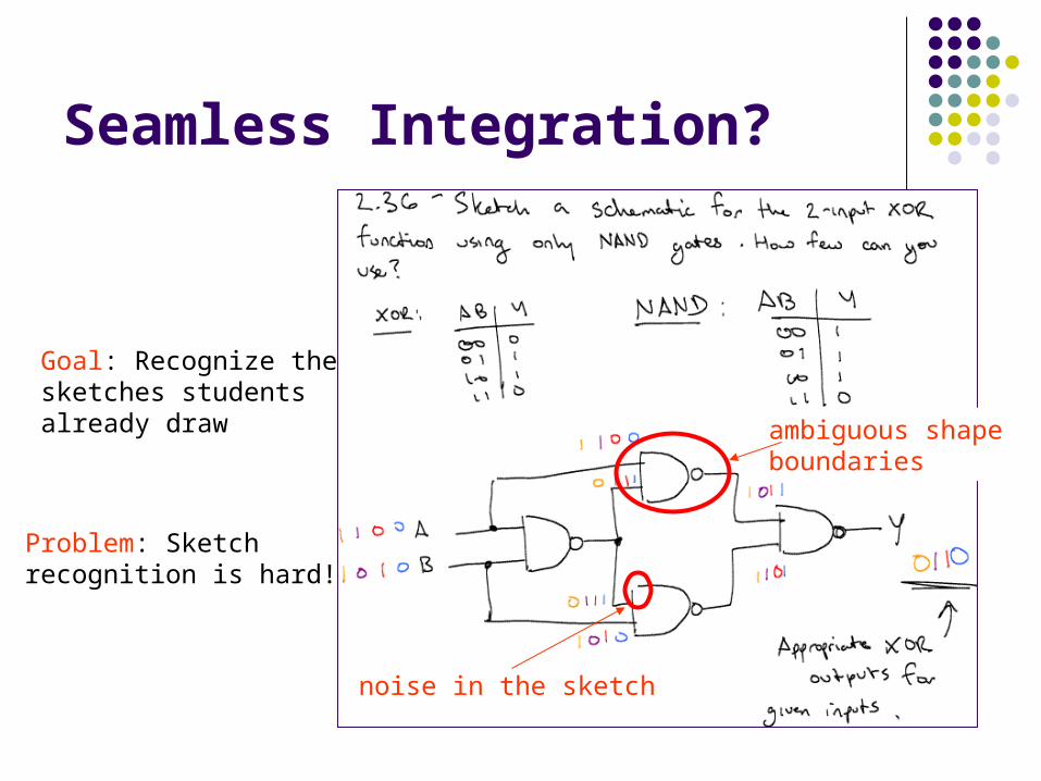
Seamless Integration?
Goal: Recognize thesketches students already draw
Problem: Sketchrecognition is hard!
noise in the sketch
ambiguous shapeboundaries

Drawing Style Restrictions
One stroke/symbol (i.e., gesture-based input)
Pause between symbols
Symbols contain temporally contiguous strokes
Are these restrictions natural?

Our study
Data collection: Problem sets, notes
labs from digital design class
Drawn in WindowsJournal (no recognition)
Measured: Number of strokes per symbol Pause time between symbols Stroke order

Dataset
98 digital circuit diagrams extracted from 13 students' notes, problem sets and labs
Stroke: time-ordered set of points (x, y, time)
Diagram: time-ordered set of strokes

Dataset: Labeling
A
wire AND OR NOT NAND NOR XOR label
Digital Logic Symbols
NAND
label
other
wire
wire

1890 54
8 507
161
817 13
3
121
68
8
12
45
439 89
16
23
334
8 4
36
2
0
16
0%10%20%30%40%50%60%70%80%90%
100%
Consecutive Non Consecutive
Results: Stroke Order
Individual range: 70% - 96%
AND
NAND
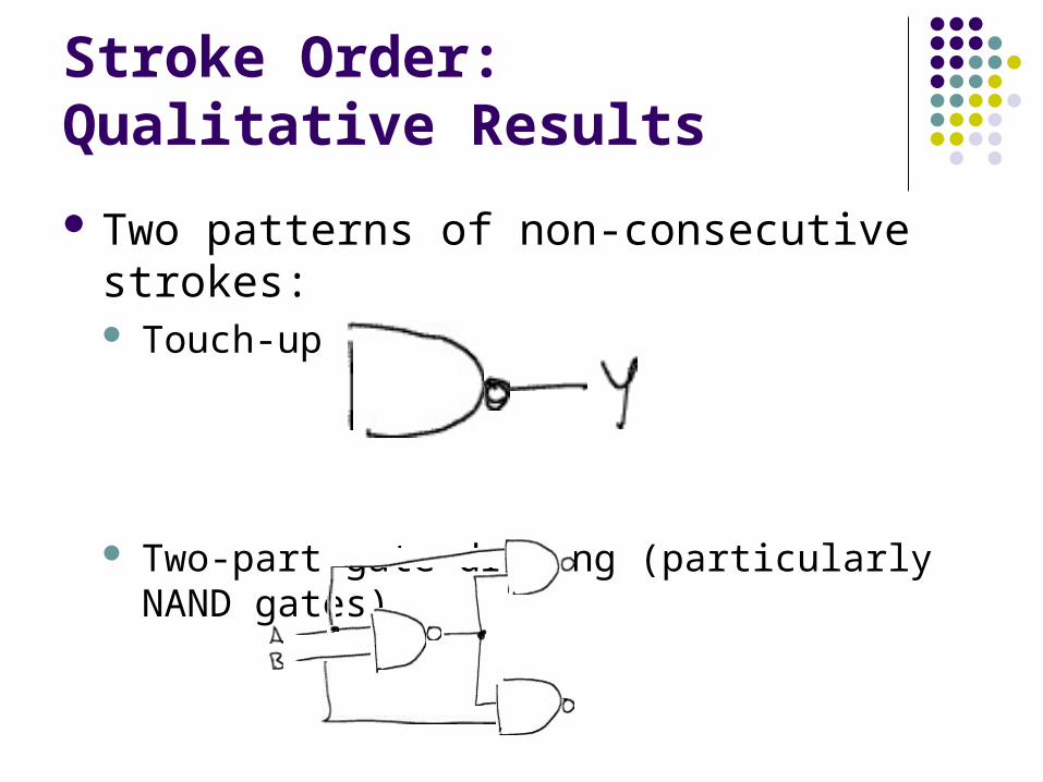
Stroke Order:Qualitative Results
Two patterns of non-consecutive strokes: Touch-up stroke
Two-part gate drawing (particularly NAND gates)

Results: Stroke Timing
0
500
1000
1500
2000
2500
3000
3500
4000
0 1 2 3 4 5 6 7 8 9 10 11 12 13
User ID
Pa
use
Tim
e (
mse
c)
Same Shape New Shape
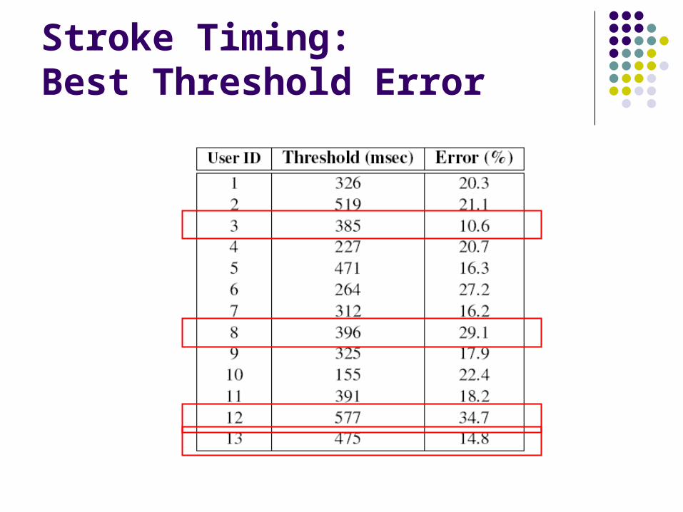
Stroke Timing: Best Threshold Error

Results: Strokes Per SymbolAND Gates
Students use a range of drawing patterns Some students consistent, some inconsistent
0%
20%
40%
60%
80%
100%
1 2 3 4 5 6 7 8 9 10 11 12 13
>= 10 Strokes9 Strokes8 Strokes 7 Strokes6 Strokes5 Strokes4 Strokes3 Strokes2 Strokes1 Stroke

0%
20%
40%
60%
80%
100%
1 2 3 4 5 6 7 8 9 10 11 12 13
1 Stroke 2 Strokes 3 Strokes 4 Strokes 5 Strokes
6 Strokes 7 Strokes 8 Strokes 9 Strokes >= 10 Strokes
0%
20%
40%
60%
80%
100%
1 2 3 4 5 6 7 8 9 10 11 12 13
Results: Strokes per SymbolAND vs. NOT
AND
NOT

Results: Strokes per Symbolwires
Most wires drawn with 1 stroke… …yet some students > 5 strokes
0%
20%
40%
60%
80%
100%
1 2 3 4 5 6 7 8 9 10 11 12 13
1 Stroke 2 Strokes 3 Strokes 4 Strokes 5 Strokes6 Strokes 7 Strokes 8 Strokes 9 Strokes >=10 Strokes
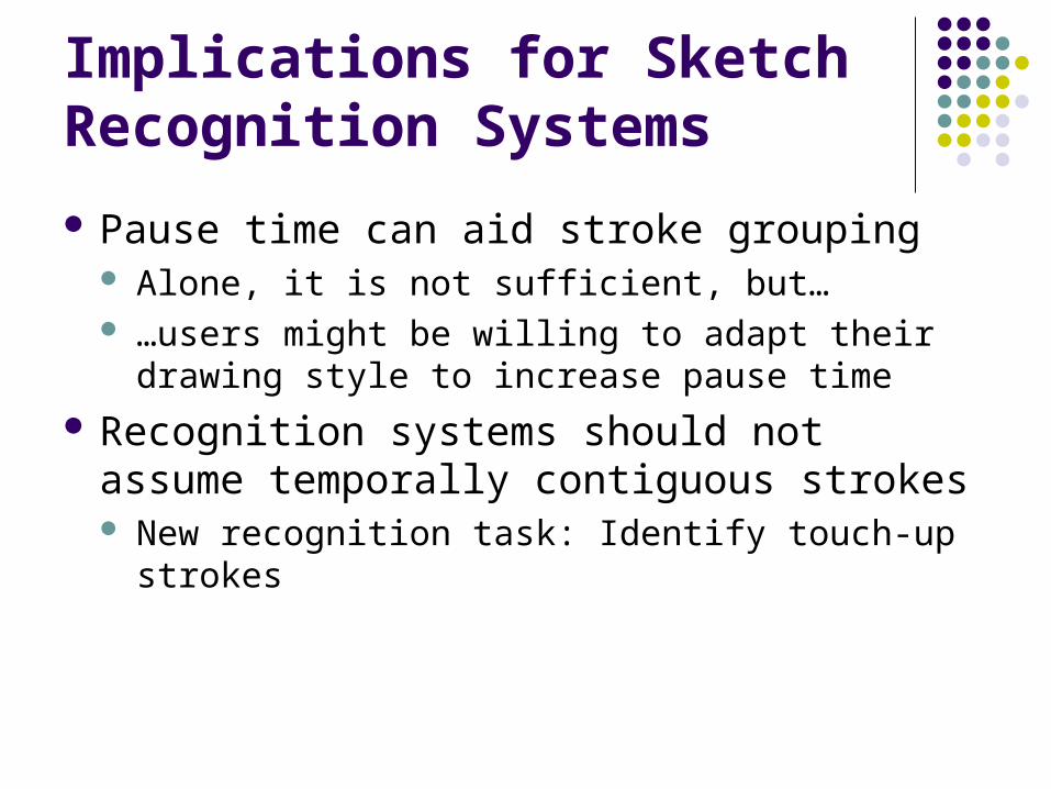
Implications for Sketch Recognition Systems
Pause time can aid stroke grouping Alone, it is not sufficient, but… …users might be willing to adapt their drawing
style to increase pause time Recognition systems should not assume
temporally contiguous strokes New recognition task: Identify touch-up strokes
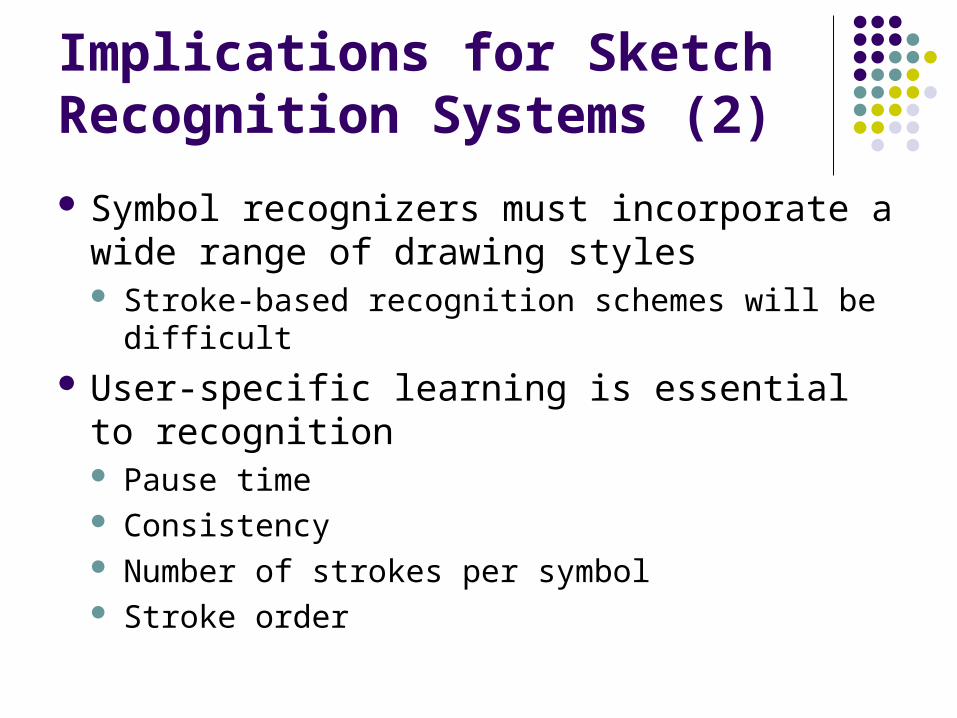
Implications for Sketch Recognition Systems (2)
Symbol recognizers must incorporate a wide range of drawing styles Stroke-based recognition schemes will be difficult
User-specific learning is essential to recognition Pause time Consistency Number of strokes per symbol Stroke order

Future work
Analyze additional domains
Front End
Circuit Recognitionand Translation
Simulation (Xilinx)
Verilog file
hand-drawn sketch
Incorporate knowledge into
recognition system design

Questions?