Embed Size (px)
Citation preview

Properties of Semiconductor Alloys:Group-IV, III–V and II–VI
Semiconductors
SADAO ADACHI
Gunma University, Gunma, Japan


Properties of Semiconductor Alloys:Group-IV, III–V and II–VI
Semiconductors
Wiley Series in Materials for Electronic & Optoelectronic Applications
Series Editors
Peter Capper, SELEX Sensors and Airborne Systems Infrared Ltd, Southampton, UKSafa Kasap, University of Saskatchewan, CanadaArthur Willoughby, University of Southampton, Southampton, UK
Published titles
Bulk Crystal Growth of Electronic, Optical and Optoelectronic Materials, Edited byP. CapperProperties of Group-IV, III–V and II–VI Semiconductors, S. AdachiCharge Transport in Disordered Solids with Applications in Electronics, Edited byS. BaranovskiOptical Properties of Condensed Matter and Applications, Edited by J. SinghThin Film Solar Cells: Fabrication, Characterization and Applications, Edited byJ. Poortmans and V. ArkhipovDielectric Films for Advanced Microelectronics, Edited by M. R. Baklanov, M. Green andK. MaexLiquid Phase Epitaxy of Electronic, Optical and Optoelectronic Materials, Edited byP. Capper and M. MaukMolecular Electronics: From Principles to Practice, M. PettyLuminescent Materials and Applications, Edited by A. KitaiCVD Diamond for Electronic Devices and Sensors, Edited by R. S. Sussman
Forthcoming Titles
Zinc Oxide Materials for Electronic and Optoelectronic Device Applications, Edited byC. Litton, D. C. Reynolds and T. C. CollinsMercury Cadmium Telluride: Growth, Properties and Applications, Edited by P. Capper andJ. GarlandPhotovoltaic Materials: From Crystalline Silicon to Third-Generation Approaches, Edited byG. J. ConibeerSilicon Photonics: Fundamentals and Devices, J. Deen and P. K. BasuInorganic Glasses for Photonics: Fundamentsls, Engineering and Applications, A. Jha, R. M.Almeida, M. Clara Goncalves and P. G. Kazansky
Properties of Semiconductor Alloys:Group-IV, III–V and II–VI
Semiconductors
SADAO ADACHI
Gunma University, Gunma, Japan
This edition first published 2009# 2009 John Wiley & Sons Ltd
Registered officeJohn Wiley & Sons Ltd, The Atrium, Southern Gate, Chichester, West Sussex, PO19 8SQ, United Kingdom
For details of our global editorial offices, for customer services and for information about how to apply forpermission to reuse the copyright material in this book please see our website at www.wiley.com.
The right of the authors to be identified as the authors of this work has been asserted in accordance with theCopyright, Designs and Patents Act 1988.
All rights reserved. No part of this publication may be reproduced, stored in a retrieval system or transmitted, in anyform or by any means, electronic, mechanical, photocopying, recording or otherwise, except as permitted by the UKCopyright, Designs and Patents Act 1988, without the prior permission of the publisher.
Wiley also publishes its books in a variety of electronic formats. Some content that appears in print may not beavailable in electronic books.
Designations used by companies to distinguish their products are often claimed as trademarks. All brand names andproduct names used in this book are trade names, service marks, trademarks or registered trademarks of theirrespective owners. The publisher is not associated with any product or vendor mentioned in this book. Thispublication is designed to provide accurate and authoritative information in regard to the subject matter covered. It issold on the understanding that the publisher is not engaged in rendering professional services. If professional adviceor other expert assistance is required, the services of a competent professional should be sought.
The publisher and the author make no representations or warranties with respect to the accuracy or completeness ofthe contents of this work and specifically disclaim all warranties, including without limitation any impliedwarranties of fitness for a particular purpose. This work is sold with the understanding that the publisher isnot engaged in rendering professional services. The advice and strategies contained herein may not be suitable forevery situation. In view of ongoing research, equipment modifications, changes in governmental regulations and theconstant flow of information relating to the use of experimental reagents, equipment and devices, the reader is urgedto review and evaluate the information provided in the package insert or instructions for each chemical, piece ofequipment, reagent or device for, among other things, any changes in the instructions or indication of usage and foradded warnings and precautions. The fact that an organization or Website is referred to in this work as a citation and/or a potential source of further information does not mean that the author or the publisher endorses the informationthe organization or Website may provide or recommendations it may make. Further, readers should be aware thatInternet Websites listed in this work may have changed or disappeared between when this work was written andwhen it is read. No warranty may be created or extended by any promotional statements for this work. Neither thepublisher nor the author shall be liable for any damages arising herefrom.
Library of Congress Cataloging-in-Publication Data
Adachi, Sadao, 1950–Properties of semiconductor alloys : group-IV, III–V and II–VI
semiconductors / Sadao Adachi.p. cm.
Includes bibliographical references and index.ISBN 978-0-470-74369-01. Semiconductors–Materials. 2. Semiconductors–Analysis.
3. Silicon alloys. I. Title.TK7871.85.A32 2009621.381502–dc22 2008046980
A catalogue record for this book is available from the British Library.
ISBN 978-0-470-74369-0 (HB)
Typeset in 10/12pt Times by Thomson Digital, Noida, India.Printed and bound in Great Britain by CPI Antony Rowe, Ltd, Chippenham, Wiltshire
Front cover image of a photodiode array reproduced by kind permission of Dr. Jian-young Wu. Courtesy of WutechInstruments and RedShirtImaging.
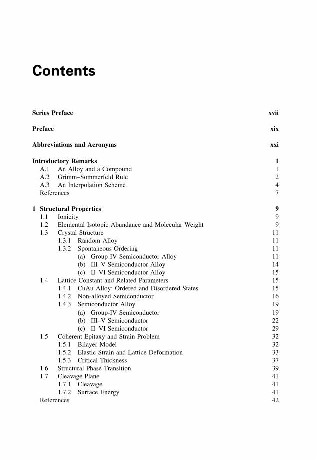
Contents
Series Preface xvii
Preface xix
Abbreviations and Acronyms xxi
Introductory Remarks 1
A.1 An Alloy and a Compound 1
A.2 Grimm–Sommerfeld Rule 2
A.3 An Interpolation Scheme 4
References 7
1 Structural Properties 9
1.1 Ionicity 9
1.2 Elemental Isotopic Abundance and Molecular Weight 9
1.3 Crystal Structure 11
1.3.1 Random Alloy 11
1.3.2 Spontaneous Ordering 11
(a) Group-IV Semiconductor Alloy 11
(b) III–V Semiconductor Alloy 14
(c) II–VI Semiconductor Alloy 15
1.4 Lattice Constant and Related Parameters 15
1.4.1 CuAu Alloy: Ordered and Disordered States 15
1.4.2 Non-alloyed Semiconductor 16
1.4.3 Semiconductor Alloy 19
(a) Group-IV Semiconductor 19
(b) III–V Semiconductor 22
(c) II–VI Semiconductor 29
1.5 Coherent Epitaxy and Strain Problem 32
1.5.1 Bilayer Model 32
1.5.2 Elastic Strain and Lattice Deformation 33
1.5.3 Critical Thickness 37
1.6 Structural Phase Transition 39
1.7 Cleavage Plane 41
1.7.1 Cleavage 41
1.7.2 Surface Energy 41
References 42
2 Thermal Properties 45
2.1 Melting Point and Related Parameters 45
2.1.1 Phase Diagram 45
(a) Group-IV Semiconductor Alloy 45
(b) III–V Semiconductor Alloy 45
(c) II–VI Semiconductor Alloy 48
2.1.2 Melting Point 51
2.2 Specific Heat 51
2.2.1 Group-IV Semiconductor Alloy 51
2.2.2 III–V Semiconductor Alloy 54
2.2.3 II–VI Semiconductor Alloy 56
2.3 Debye Temperature 56
2.3.1 General Considerations 56
2.3.2 Group-IV Semiconductor Alloy 57
2.3.3 III–V Semiconductor Alloy 58
2.3.4 II–VI Semiconductor Alloy 58
2.4 Thermal Expansion Coefficient 59
2.4.1 Group-IV Semiconductor Alloy 59
2.4.2 III–V Semiconductor Alloy 61
2.4.3 II–VI Semiconductor Alloy 63
2.5 Thermal Conductivity and Diffusivity 63
2.5.1 Thermal Conductivity 63
(a) General Considerations 63
(b) Group-IV Semiconductor Alloy 66
(c) III–V Semiconductor Alloy 68
(d) II–VI Semiconductor Alloy 74
2.5.2 Thermal Diffusivity 75
(a) General Considerations 75
(b) Alloy Value 75
References 76
3 Elastic Properties 81
3.1 Elastic Constant 81
3.1.1 General Considerations 81
3.1.2 Room-temperature Value 81
(a) Group-IV Semiconductor Alloy 81
(b) III–V Semiconductor Alloy 81
(c) II–VI Semiconductor Alloy 84
3.1.3 External Perturbation Effect 86
(a) Temperature Effect 86
(b) Pressure Effect 88
3.2 Third-order Elastic Constant 89
3.3 Young’s Modulus, Poisson’s Ratio and Similar Properties 89
3.3.1 Group-IV Semiconductor Alloy 89
3.3.2 III–V Semiconductor Alloy 89
3.3.3 II–VI Semiconductor Alloy 90
vi CONTENTS
3.4 Microhardness 92
3.4.1 Group-IV Semiconductor Alloy 92
3.4.2 III–V Semiconductor Alloy 92
3.4.3 II–VI Semiconductor Alloy 93
3.5 Sound Velocity 96
References 97
4 Lattice Dynamic Properties 99
4.1 Phonon Dispersion Relationships 99
4.2 Phonon Frequency 99
4.2.1 General Considerations 99
4.2.2 Room-temperature Value 100
(a) Group-IV Semiconductor Alloy 100
(b) III–V Semiconductor Alloy 104
(c) II–VI Semiconductor Alloy 109
4.2.3 External Perturbation Effect 112
(a) Group-IV Semiconductor Alloy 112
(b) III–V Semiconductor Alloy 113
(c) II–VI Semiconductor Alloy 115
4.3 Mode Gr€uneisen Parameter 119
4.3.1 Phonon Deformation Potential 121
References 123
5 Collective Effects and Some Response Characteristics 125
5.1 Piezoelectric Constant 125
5.1.1 General Considerations 125
5.1.2 Alloy Value 125
5.2 Fr€ohlich Coupling Constant 129
5.2.1 General Considerations 129
5.2.2 Alloy Value 129
References 131
6 Energy-band Structure: Energy-band Gaps 133
6.1 Introductory Remarks 133
6.1.1 Quasi-cubic Band Model 133
6.1.2 Bowing Parameter 136
6.1.3 Ordered Alloy 136
6.2 Group-IV Semiconductor Alloy 139
6.2.1 Binary Alloy 139
(a) CSi 139
(b) CGe 140
(c) SiGe 141
(d) GeSn 144
6.2.2 Ternary Alloy 145
(a) CSiGe 145
(b) SiGeSn 147
6.2.3 Summary 147
CONTENTS vii
6.3 III–V Semiconductor Ternary Alloy 149
6.3.1 (III, III)–N Alloy 149
(a) c-AlGaN 149
(b) w-AlGaN 150
(c) c-AlInN 152
(d) w-AlInN 152
(e) c-GaInN 152
(f) w-GaInN 152
6.3.2 (III, III)–P Alloy 153
(a) AlGaP 153
(b) AlInP 153
(c) GaInP 155
6.3.3 (III, III)–As Alloy 157
(a) AlGaAs 157
(b) AlInAs 160
(c) GaInAs 161
6.3.4 (III, III)–Sb Alloy 163
(a) AlGaSb 163
(b) AlInSb 165
(c) GaInSb 166
6.3.5 Dilute-nitride III–(V, V) Alloy 166
(a) General Considerations 166
(b) GaNP 170
(c) GaNAs 171
(d) GaNSb 172
(e) InNP 173
(f) InNAs 173
(g) InNSb 174
6.3.6 Al–(V, V) Alloy 174
6.3.7 Ga–(V, V) Alloy 175
(a) GaPAs 175
(b) GaPSb 176
(c) GaAsSb 178
6.3.8 In–(V, V) Alloy 179
(a) InPAs 179
(b) InPSb 179
(c) InAsSb 181
6.3.9 Summary 183
6.4 III–V Semiconductor Quaternary Alloy 184
6.4.1 Dilute-nitride Quaternary Alloy 184
(a) AlGaNAs 184
(b) GaInNP 185
(c) GaInNAs 185
(d) GaNPAs 185
6.4.2 (III, III)–(V, V) Alloy 186
(a) AlGaPAs 186
(b) AlGaAsSb 187
viii CONTENTS
(c) AlInAsSb 188
(d) GaInPAs 189
(e) GaInAsSb 191
6.4.3 (III, III, III)–V Alloy 193
(a) AlGaInP 193
(b) AlGaInAs 194
6.4.4 III–(V, V, V) Alloy 195
6.4.5 Summary 196
6.5 II–VI Semiconductor Alloy 197
6.5.1 (II, II)–O Ternary Alloy 197
(a) BeZnO 197
(b) MgZnO 197
(c) ZnCdO 198
6.5.2 (II, II)–S Ternary Alloy 198
(a) MgZnS 198
(b) ZnCdS 200
(c) ZnHgS 200
(d) CdHgS 200
6.5.3 (II, II)–Se Ternary Alloy 201
(a) BeZnSe 201
(b) BeCdSe 202
(c) MgZnSe 202
(d) MgCdSe 202
(e) ZnCdSe 203
(f) CdHgSe 203
6.5.4 (II, II)–Te Ternary Alloy 204
(a) BeZnTe 204
(b) MgZnTe 205
(c) MgCdTe 206
(d) ZnCdTe 206
(e) ZnHgTe 207
(f) CdHgTe 208
6.5.5 Zn–(VI, VI) Ternary Alloy 208
(a) ZnOS 208
(b) ZnOSe 209
(c) ZnSSe 209
(d) ZnSTe 210
(e) ZnSeTe 210
6.5.6 Cd–(VI, VI) Ternary Alloy 210
(a) CdSSe 210
(b) CdSTe 211
(c) CdSeTe 211
6.5.7 (II, II)–(VI, VI) Quaternary Alloy 212
(a) MgZnSSe 212
(b) MgZnSeTe 213
6.5.8 (II, II, II)–VI Quaternary Alloy 213
(a) BeMgZnSe 213
CONTENTS ix
(b) BeZnCdSe 213
(c) MgZnCdSe 214
6.5.9 Summary 214
References 216
7 Energy-band Structure: Effective Masses 229
7.1 Introductory Remarks 229
7.1.1 Electron Effective Mass 229
7.1.2 Hole Effective Mass 230
7.1.3 Interpolation Scheme 232
7.2 Group-IV Semiconductor Alloy 234
7.2.1 CSi Binary Alloy 234
7.2.2 SiGe Binary Alloy 237
7.3 III–V Semiconductor Ternary Alloy 238
7.3.1 (III, III)–N Alloy 238
7.3.2 (III, III)–P Alloy 238
7.3.3 (III, III)–As Alloy 239
(a) AlGaAs 239
(b) AlInAs 241
(c) GaInAs 241
7.3.4 (III, III)–Sb Alloy 242
7.3.5 Dilute-nitride III–(V, V) Alloy 243
(a) Ga–(N, V) Alloy 243
(b) In–(N, V) Alloy 244
7.3.6 Al–(V, V) Alloy 245
7.3.7 Ga–(V, V) Alloy 245
(a) GaPAs 245
(b) GaAsSb 246
7.3.8 In–(V, V) Alloy 246
(a) InPAs 246
(b) InAsSb 247
7.4 III–V Semiconductor Quaternary Alloy 248
7.4.1 Dilute-nitride Quaternary Alloy 248
7.4.2 (III, III)–(V, V) Alloy 248
(a) GaInPAs 248
(b) GaInAsSb 249
7.4.3 (III, III, III)–V Alloy 250
(a) AlGaInP 250
(b) AlGaInAs 250
7.4.4 III–(V, V, V) Alloy 250
7.5 II–VI Semiconductor Alloy 251
7.5.1 (II, II)–VI Ternary Alloy 251
7.5.2 II–(VI, VI) Ternary Alloy 253
7.5.3 (II, II)–(VI, VI) Quaternary Alloy 253
7.6 Concluding Remarks 254
7.6.1 Composition Dependence 254
7.6.2 External Perturbation Effect 254
References 256
x CONTENTS
8 Deformation Potentials 259
8.1 Intravalley Deformation Potential: � Point 259
8.1.1 Group-IV Semiconductor Alloy 259
8.1.2 III–V Semiconductor Ternary Alloy 261
(a) AlGaN 261
(b) GaInN 262
(c) AlInP 262
(d) GaInP 263
(e) AlGaAs 263
(f) AlInAs 264
(g) GaInAs 265
(h) GaNAs 265
(i) GaPAs 266
8.1.3 III–V Semiconductor Quaternary Alloy 266
8.1.4 II–VI Semiconductor Alloy 266
8.2 Intravalley Deformation Potential: High-symmetry
Points 267
8.2.1 Group-IV Semiconductor Alloy 267
8.2.2 III–V Semiconductor Alloy 269
8.2.3 II–VI Semiconductor Alloy 270
8.3 Intervalley Deformation Potential 270
8.3.1 Group-IV Semiconductor Alloy 270
8.3.2 III–V Semiconductor Alloy 271
8.3.3 II–VI Semiconductor Alloy 272
References 272
9 Heterojunction Band Offsets and Schottky Barrier
Height 275
9.1 Heterojunction Band Offsets 275
9.1.1 General Considerations 275
9.1.2 Group-IV Semiconductor Heterostructure System 275
(a) CSi/Si 275
(b) SiGe/Si 276
(c) CSiGe/Si 276
(d) CSi/SiGe 277
9.1.3 III–V Semiconductor Heterostructure System:
Lattice-matched Ternary-alloy System 277
(a) GaInP/GaAs 277
(b) GaInP/AlInP 277
(c) GaInP/AlGaAs 278
(d) AlGaAs/GaAs 278
(e) AlInAs/InP 279
(f) GaInAs/InP 279
(g) GaInAs/AlInAs 280
(h) InAsSb/GaSb 280
9.1.4 III–V Semiconductor Heterostructure System:
Lattice-matched Quaternary Alloy 280
(a) GaInPAs/InP 280
CONTENTS xi
(b) AlGaAsSb/GaSb 281
(c) AlGaAsSb/InP 281
(d) AlGaAsSb/InAs 281
(e) GaInAsSb/GaSb 281
(f) GaInAsSb/InP 281
(g) GaInAsSb/InAs 281
(h) AlGaAsSb/GaInAsSb 282
(i) AlInAsSb/GaInAsSb 282
(j) AlGaInP/AlInP 282
(k) AlGaInP/GaInP 282
(l) AlGaInAs/GaInAs 283
9.1.5 III–V Semiconductor Heterostructure System:
Lattice-mismatched Alloy System 283
(a) w-AlGaN/w-GaN 283
(b) w-AlInN/w-InN 284
(c) w-GaInN/w-GaN 284
(d) GaInAs/GaAs 284
(e) Dilute-nitride-based Heterostructure System 286
9.1.6 II–VI Semiconductor Heterostructure System 287
(a) (II, II)–O-based Heterostructure System 287
(b) (II, II)–S-based Heterostructure System 287
(c) (II, II)–Se-based Heterostructure System 287
(d) (II, II)–Te-based Heterostructure System 288
(e) Zn–(VI, VI)-based Heterostructure System 289
(f) (II, II)–VI-based and II–(VI, VI)-based Heterostructure
Systems 289
(g) (II, II)–(VI, VI)-based Heterostructure System 289
(h) (II, II, II)–VI-based Heterostructure System 289
9.2 Schottky Barrier Height 289
9.2.1 General Considerations 289
9.2.2 Group-IV Semiconductor Alloy 290
(a) SiGe Binary Alloy 290
(b) CSiGe Ternary Alloy 291
9.2.3 III–V Semiconductor Ternary Alloy 291
(a) (III, III)–N Alloy 291
(b) (III, III)–P Alloy 292
(c) (III, III)–As Alloy 292
(d) (III, III)–Sb Alloy 294
(e) Ga–(V, V) Alloy 295
9.2.4 III–V Semiconductor Quaternary Alloy 296
(a) (III, III)–(V, V) Alloy 296
(b) (III, III, III)–V Alloy 297
9.2.5 II–VI Semiconductor Alloy 299
(a) (II, II)–Te Ternary Alloy 299
(b) Zn–(VI, VI) Ternary Alloy 300
References 300
xii CONTENTS
10 Optical Properties 307
10.1 Introductory Remarks 307
10.1.1 Optical Dispersion Relations 307
10.1.2 Static and High-frequency Dielectric Constants 308
10.2 Group-IV Semiconductor Alloy 308
10.2.1 Binary Alloy 308
(a) CSi 308
(b) CGe 309
(c) SiGe 309
(d) GeSn 310
10.2.2 Ternary Alloy 311
10.3 III–V Semiconductor Ternary Alloy 311
10.3.1 (III, III)–N Alloy 311
(a) c-(III, III)–N Alloy 311
(b) w-AlGaN 312
(c) w-AlInN 313
(d) w-GaInN 313
10.3.2 (III, III)–P Alloy 314
(a) AlGaP 314
(b) AlInP 314
(c) GaInP 315
10.3.3 (III, III)–As Alloy 316
(a) AlGaAs 316
(b) AlInAs 316
(c) GaInAs 318
10.3.4 (III, III)–Sb Alloy 319
(a) AlGaSb 319
(b) GaInSb 319
10.3.5 Dilute-nitride III–(V, V) Alloy 320
(a) GaNP 320
(b) GaNAs 321
(c) GaNSb 321
(d) InNP 322
(e) InNAs 322
10.3.6 Al–(V, V) Alloy 322
10.3.7 Ga–(V, V) Alloy 323
(a) GaPAs 323
(b) GaPSb 324
(c) GaAsSb 324
10.3.8 In–(V, V) Alloy 324
(a) InPAs 324
(b) InPSb 325
(c) InAsSb 325
10.4 III–V Semiconductor Quaternary Alloy 326
10.4.1 Dilute-nitride Quaternary Alloy 326
(a) GaInNP 326
(b) GaInNAs 326
CONTENTS xiii
10.4.2 (III, III)–(V, V) Alloy 326
(a) AlGaPAs 326
(b) AlGaAsSb 327
(c) GaInPAs 327
(d) GaInAsSb 328
10.4.3 (III, III, III)–V Alloy 330
(a) AlGaInP 330
(b) AlGaInAs 331
10.4.4 III–(V, V, V) Alloy 332
10.5 II–VI Semiconductor Alloy 332
10.5.1 (II, II)–O Ternary Alloy 332
(a) BeZnO 332
(b) MgZnO 332
(c) ZnCdO 333
10.5.2 (II, II)–S Ternary Alloy 333
(a) MgZnS 333
(b) ZnCdS 334
10.5.3 (II, II)–Se Ternary Alloy 335
(a) BeZnSe 335
(b) BeCdSe 335
(c) MgZnSe 335
(d) MgCdSe 337
(e) ZnCdSe 337
(f) CdHgSe 338
10.5.4 (II, II)–Te Ternary Alloy 339
(a) BeZnTe 339
(b) MgZnTe 339
(c) MgCdTe 340
(d) ZnCdTe 340
(e) ZnHgTe 342
(f) CdHgTe 342
10.5.5 Zn–(VI, VI) Ternary Alloy 343
(a) ZnOS 343
(b) ZnSSe 343
(c) ZnSTe 343
(d) ZnSeTe 344
10.5.6 Cd–(VI, VI) Ternary Alloy 344
(a) CdSSe 344
(b) CdSTe 345
(c) CdSeTe 346
10.5.7 (II, II)–(VI, VI) Quaternary Alloy 346
(a) MgZnSSe 346
(b) MgZnSeTe 346
10.5.8 (II, II, II)–VI Quaternary Alloy 346
(a) BeMgZnSe 346
(b) BeZnCdSe 346
(c) MgZnCdSe 346
References 347
xiv CONTENTS
11 Elasto-optic, Electro-optic and Nonlinear Optical
Properties 357
11.1 Elasto-optic Effect 357
11.1.1 Group-IV Semiconductor Alloy 357
11.1.2 III–V Semiconductor Alloy 357
11.1.3 II–VI Semiconductor Alloy 357
11.2 Linear Electro-optic Constant 358
11.2.1 Group-IV Semiconductor Alloy 358
11.2.2 III–V Semiconductor Alloy 358
11.2.3 II–VI Semiconductor Alloy 358
11.3 Quadratic Electro-optic Constant 360
11.3.1 Group-IV Semiconductor Alloy 360
11.3.2 III–V Semiconductor Alloy 360
11.3.3 II–VI Semiconductor Alloy 360
11.4 Franz–Keldysh Effect 360
11.4.1 Group-IV Semiconductor Alloy 360
11.4.2 III–V Semiconductor Alloy 360
11.4.3 II–VI Semiconductor Alloy 360
11.5 Nonlinear Optical Constant 361
11.5.1 Group-IV Semiconductor Alloy 361
11.5.2 III–V Semiconductor Alloy 361
11.5.3 II–VI Semiconductor Alloy 362
References 362
12 Carrier Transport Properties 365
12.1 Introductory Remarks 365
12.2 Low-field Mobility 367
12.2.1 Group-IV Semiconductor Alloy 367
(a) CSi Binary Alloy 367
(b) SiGe Binary Alloy 367
12.2.2 III–V Semiconductor Ternary Alloy 368
(a) (III, III)–N Alloy 368
(b) (III, III)–P Alloy 369
(c) (III, III)–As Alloy 369
(d) (III, III)–Sb Alloy 369
(e) Dilute-nitride III–(V, V) Alloy 371
(f) Ga–(V, V) Alloy 371
(g) In–(V, V) Alloy 371
12.2.3 III–V Semiconductor Quaternary Alloy 371
(a) Dilute-nitride Alloy 371
(b) (III, III)–(V, V) Alloy 372
(c) (III, III, III)–V Alloy 373
12.2.4 II–VI Semiconductor Alloy 374
(a) (II, II)–O Ternary Alloy 374
(b) (II, II)–Se Ternary Alloy 374
(c) (II, II)–Te Ternary Alloy 375
(d) Zn–(V, V) Ternary Alloy 376
CONTENTS xv
12.3 High-field Transport 376
12.3.1 Group-IV Semiconductor Alloy 376
12.3.2 III–V Semiconductor Ternary Alloy 376
(a) (III, III)–N Alloy 376
(b) (III, III)–P Alloy 376
(c) (III, III)–As Alloy 377
(d) Dilute-nitride III–(V, V) Alloy 378
12.3.3 III–V Semiconductor Quaternary Alloy 378
12.3.4 II–VI Semiconductor Alloy 379
12.4 Minority-carrier Transport 379
12.4.1 Group-IV Semiconductor Alloy 379
(a) SiGe Binary Alloy 379
(b) CSiGe Ternary Alloy 380
12.4.2 III–V Semiconductor Ternary Alloy 380
(a) (III, III)–N Alloy 380
(b) (III, III)–As Alloy 380
(c) Ga–(V, V) Alloy 381
12.4.3 III–V Semiconductor Quaternary Alloy 381
(a) (III, III)–(V, V) Alloy 381
(b) (III, III, III)–V Alloy 382
12.4.4 II–VI Semiconductor Alloy 382
12.5 Impact Ionization Coefficient 382
12.5.1 Group-IV Semiconductor Alloy 382
12.5.2 III–V Semiconductor Ternary Alloy 382
(a) (III, III)–N Alloy 382
(b) (III, III)–P Alloy 383
(c) (III, III)–As Alloy 383
(d) (III, III)–Sb Alloy 384
(e) Dilute-nitride III–(V, V) Alloy 384
(f) Ga–(V, V) Alloy 385
(g) In–(V, V) Alloy 385
12.5.3 III–V Semiconductor Quaternary Alloy 385
(a) (III, III)–(V, V) Alloy 385
(b) (III, III, III)–V Alloy 385
12.5.4 II–VI Semiconductor Alloy 386
References 386
Index 391
xvi CONTENTS
Series Preface
WILEY SERIES IN MATERIALS FOR ELECTRONIC ANDOPTOELECTRONIC APPLICATIONS
This book series is devoted to the rapidly developing class of materials used for electronic andoptoelectronic applications. It is designed to provide much-needed information on thefundamental scientific principles of these materials, together with how these are employedin technological applications. The books are aimed at (postgraduate) students, researchers andtechnologists, engaged in research, development and the study of materials in electronics andphotonics, and industrial scientists developing new materials, devices and circuits for theelectronic, optoelectronic and communications industries.
The development of new electronic and optoelectronic materials depends not only onmaterials engineering at a practical level, but also on a clear understanding of the properties ofmaterials, and the fundamental science behind these properties. It is the properties of amaterialthat eventually determine its usefulness in an application. The series therefore also includessuch titles as electrical conduction in solids, optical properties, thermal properties, and so on,all with applications and examples of materials in electronics and optoelectronics. Thecharacterization of materials is also covered within the series in as much as it is impossibleto develop new materials without the proper characterization of their structure and properties.Structure-property relationships have always been fundamentally and intrinsically importantto materials science and engineering.
Materials science is well known for being one of themost interdisciplinary sciences. It is theinterdisciplinary aspect of materials science that has led to many exciting discoveries, newmaterials and new applications. It is not unusual to find scientists with a chemical engineeringbackground working on materials projects with applications in electronics. In selecting titlesfor the series, we have tried to maintain the interdisciplinary aspect of the field, and hence itsexcitement to researchers in this field.
Peter CapperSafa Kasap
Arthur Willoughby

Preface
Semiconductor alloys provide a natural means of tuning the magnitude of the band-gap energyand other material properties so as to optimize and widen the application of semiconductordevices. Current research and development in semiconductor alloys is focused on areas ofimproved materials growth, development of unique materials characterization and suitableprocess technologies, fabrication of novel devices using artificially controlled materialsstructures and better understanding of degradation mechanisms in electronic and optoelec-tronic devices for improved device reliability.
Even though the basic semiconductor alloy concepts are understood at this time, thedetermination of some device parameters has been hampered by a lackof definite knowledge ofmany material parameters. The main purpose of this book is to provide a comprehensivetreatment of the materials aspects of group-IV, III�Vand II�VI semiconductor alloys used invarious electronic and optoelectronic devices. The topics treated in this book include thestructural, thermal, mechanical, lattice vibronic, electronic, optical and carrier transportproperties of such semiconductor alloys. The book covers not only commonly known alloys(SiGe, AlGaAs, GaInPAs, ZnCdTe, etc.) but also new alloys, such as dilute-carbon alloys(CSiGe, CSiSn, etc.), III�N alloys, dilute-nitride alloys (GaNAs, GaInNAs, etc.) and Mg- orBe-based II�VI semiconductor alloys.
The reader may also find the companion book �Properties of Group-IV, III�V and II�VISemiconductors� published in this series useful since it emphasizes the endpoint semiconductorprinciples and properties.
The extensive bibliography is included for those who wish to find additional information ifrequired. It is hoped that the book will attract the attention of not only semiconductor deviceengineers, but also solid-state physicists andmaterials scientists, and particularly postgraduatestudents, R&D staff and teaching and research professionals.
Sadao Adachi,Gunma University, Japan

Abbreviations and Acronyms
BAC band anticrossing
bct body-centered tetragonal
BZ Brillouin zone
c- cubic-
CB conduction band
CL cathodoluminescence
Cl-VPE chloride-transport vapor-phase epitaxy
CP critical point
CR cyclotron resonance
C–V capacitance–voltage
CVD chemical vapor deposition
DLTS deep-level transient spectroscopy
DOS density of states
DP deformation potential
ER electroreflectance
EXAFS extended X-ray absorption fine-structure spectroscopy
fcc face-centered cubic
FET field effect transistor
FTIR Fourier transform infrared
HBT heterojunction bipolar transistor
HH heavy-hole
HREELS high-resolution electron-energy-loss spectroscopy
HRXRD high-resolution X-ray diffraction
HT-VPE hydride-transport vapor-phase epitaxy
IR infrared
I–V current–voltage
LA longitudinal acoustic
LH light-hole
LO longitudinal optical
LPE liquid-phase epitaxy
MBE molecular beam epitaxy
MDF model dielectric function
MOCVD metalorganic chemical vapor deposition
MOMBE metalorganic molecular beam epitaxy
MQW multiple quantum well
MREI modified random-element-isodisplacement
PDP phonon deformation potential
PIXE particle-induced X-ray emission
PL photoluminescence
PLD pulsed-laser deposition
PLE photoluminescence excitation
PR photoreflectance
PzR piezoreflectance
QW quantum well
RBS Rutherford backscattering spectrometry
rf radio-frequency
RHEED reflection high-energy electron diffraction
SE spectroscopic ellipsometry
SL superlattice
SO spin–orbit
TA transverse acoustic
TEM transmission electron microscopy
THM traveling heater method
TO transverse optical
TP triple-period
TR thermoreflectance
UHV ultrahigh vacuum
UV ultraviolet
VB valence band
VCA virtual crystal approximation
VPE vapor-phase epitaxy
w- wurtzite
WDXS wavelength-dispersive X-ray spectroscopy
XPS X-ray photoelectron spectroscopy
XRD X-ray diffraction
1D one-dimensional
2D two-dimensional
3D three-dimensional
xxii ABBREVIATIONS AND ACRONYMS
Introductory Remarks
A.1 AN ALLOYAND A COMPOUND
An alloy is a combination, either in solution or compound, of two or more elements. An alloywith two components is called a binary alloy; onewith three is a ternary alloy; onewith four is aquaternary alloy; onewith five is a pentanary alloy. The resulting alloy substance generally hasproperties significantly different from those of its components. The proportions of theingredients are available.
A chemical compound is a substance consisting of two or more chemical elements that arechemically combined in fixed proportions. The ratio of each element is usually expressed bychemical formula. For example,water is a compound consisting of twohydrogen atoms bondedto an oxygen atom (H2O). The atoms within a compound can be held together by a variety ofinteractions, ranging from covalent bonds to electrostatic forces in ionic bonds. A continuumofbond polarities exists between the purely covalent and ionic bonds. For example, H2O is heldtogether by polar covalent bonds. NaCl is an example of an ionic compound.
Simply, an alloy is formed from a physical mixture of two or more substances, while acompound is formed from a chemical reaction. An alloy crystal is sometimes called a mixedcrystal or a solid solution. For example, GaAs is a compound consisting of Ga atoms bonded toAs atoms. It is not an alloy. AlxGa1�xAs is an alloy compound consisting of AlAs and GaAswith amole ratio of x:(1� x). The bonds in GaAs andAlAs are not adequately described by anyof these extreme types, but have characteristics intermediate to those usually associated withthe covalent and ionic terms. The bonds in diamond, C�C, can be described by the covalentbond term only. It is an elemental semiconductor, not a compound semiconductor. Similarly, Siand Ge are elemental semiconductors. Like AlxGa1�xAs, SixGe1�x (0� x� 1.0) is an alloysemiconductor. The bonds Si�Ge, Si�Si and Ge�Ge in SixGe1�x are, therefore, described bythe covalent term only. It should be noted, however, that silicon carbide (SiC) is a compound,not an alloy. This is because that the chemical bonds in SiC cannot be described only by thecovalent term, but have characteristics intermediate to those associated with the covalent andionic terms, like GaAs and AlAs.
There is an ordered alloy phase in SixGe1�x binary alloy [1]. This phase exhibits long-rangeorder rather than random arrangement of atoms as expected previously. The ordered phase, asexpected, occurs mostly in bulk SixGe1�x layers at x� 0.5 and can be explained by therhombohedral structure. Note that SiC is thought to be an ordered alloy. It crystallizes in a largenumber of polytypes. The various types of SiC differ one from another only by the order inwhich successive planes of Si (or C) atoms are stacked along the c axis; one polytype is thecubic, zinc-blende structure (3C) while the reminder, including two of the more frequentlyoccurring forms, 6H (hexagonal) and 15R (rhombohedral), possess uniaxial symmetry [2].There is no diamond structure in the SiC polytypes. An ordered alloy phase has been found notonly in SixGe1�x, but also in many III–V and II–VI semiconductor alloys [3].
Properties of Semiconductor Alloys: Group-IV, III-V and II-VI Semiconductors Sadao Adachi
�2009 John Wiley & Sons, Ltd
A.2 GRIMM–SOMMERFELD RULE
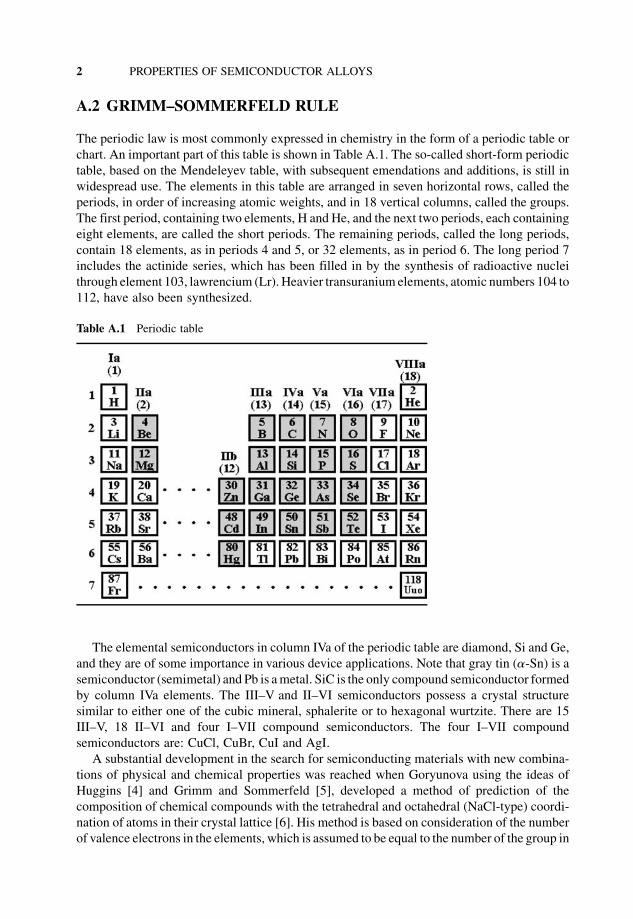
The periodic law is most commonly expressed in chemistry in the form of a periodic table orchart. An important part of this table is shown in Table A.1. The so-called short-form periodictable, based on the Mendeleyev table, with subsequent emendations and additions, is still inwidespread use. The elements in this table are arranged in seven horizontal rows, called theperiods, in order of increasing atomic weights, and in 18 vertical columns, called the groups.The first period, containing two elements, H and He, and the next two periods, each containingeight elements, are called the short periods. The remaining periods, called the long periods,contain 18 elements, as in periods 4 and 5, or 32 elements, as in period 6. The long period 7includes the actinide series, which has been filled in by the synthesis of radioactive nucleithrough element 103, lawrencium (Lr). Heavier transuranium elements, atomic numbers 104 to112, have also been synthesized.
The elemental semiconductors in column IVa of the periodic table are diamond, Si and Ge,and they are of some importance in various device applications. Note that gray tin (a-Sn) is asemiconductor (semimetal) and Pb is ametal. SiC is the only compound semiconductor formedby column IVa elements. The III–V and II–VI semiconductors possess a crystal structuresimilar to either one of the cubic mineral, sphalerite or to hexagonal wurtzite. There are 15III–V, 18 II–VI and four I–VII compound semiconductors. The four I–VII compoundsemiconductors are: CuCl, CuBr, CuI and AgI.
A substantial development in the search for semiconducting materials with new combina-tions of physical and chemical properties was reached when Goryunova using the ideas ofHuggins [4] and Grimm and Sommerfeld [5], developed a method of prediction of thecomposition of chemical compounds with the tetrahedral and octahedral (NaCl-type) coordi-nation of atoms in their crystal lattice [6]. His method is based on consideration of the numberof valence electrons in the elements, which is assumed to be equal to the number of the group in
Table A.1 Periodic table
2 PROPERTIES OF SEMICONDUCTOR ALLOYS
the periodic table towhich they belong (so-called full or normal valency) and can be expressedin the form of the equation system [7]
XAi¼1
Bixi¼4
Xni¼1
Bixi¼XAi¼nþ1
ð8�BiÞxiXAi¼1
xi¼1
ðA:1Þ
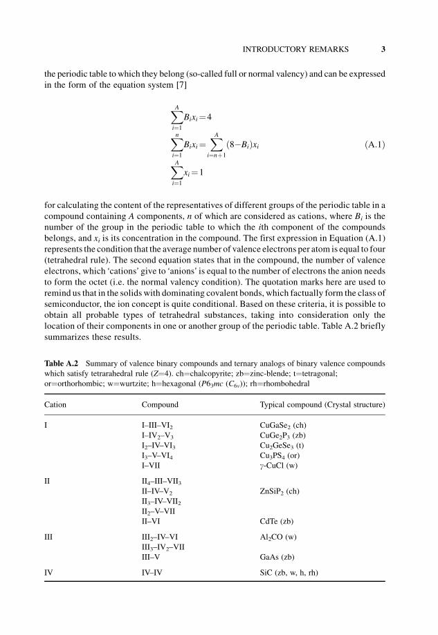
for calculating the content of the representatives of different groups of the periodic table in acompound containing A components, n of which are considered as cations, where Bi is thenumber of the group in the periodic table to which the ith component of the compoundsbelongs, and xi is its concentration in the compound. The first expression in Equation (A.1)represents the condition that the average number of valence electrons per atom is equal to four(tetrahedral rule). The second equation states that in the compound, the number of valenceelectrons, which �cations� give to �anions� is equal to the number of electrons the anion needsto form the octet (i.e. the normal valency condition). The quotation marks here are used toremind us that in the solids with dominating covalent bonds, which factually form the class ofsemiconductor, the ion concept is quite conditional. Based on these criteria, it is possible toobtain all probable types of tetrahedral substances, taking into consideration only thelocation of their components in one or another group of the periodic table. Table A.2 brieflysummarizes these results.
Table A.2 Summary of valence binary compounds and ternary analogs of binary valence compoundswhich satisfy tetrarahedral rule (Z¼4). ch¼chalcopyrite; zb¼zinc-blende; t¼tetragonal;or¼orthorhombic; w¼wurtzite; h¼hexagonal (P63mc (C6v)); rh¼rhombohedral
Cation Compound Typical compound (Crystal structure)
I I–III–VI2 CuGaSe2 (ch)I–IV2–V3 CuGe2P3 (zb)I2–IV–VI3 Cu2GeSe3 (t)I3–V–VI4 Cu3PS4 (or)I–VII g-CuCl (w)
II II4–III–VII3II–IV–V2 ZnSiP2 (ch)II3–IV–VII2II2–V–VIIII–VI CdTe (zb)
III III2–IV–VI Al2CO (w)III3–IV2–VIIIII–V GaAs (zb)
IV IV–IV SiC (zb, w, h, rh)
INTRODUCTORY REMARKS 3
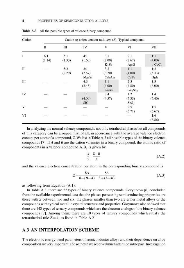
In analyzing the normal valency compounds, not only tetrahedral phases but all compoundsof this category can be grouped, first of all, in accordance with the average valence electroncontent per atom of a compound, Z. We list in Table A.3 all possible types of the binary valencecompounds [7]. If A and B are the cation valencies in a binary compound, the atomic ratio ofcomponents in a valence compound AxBy is given by
x
y¼8�B
AðA:2Þ
and the valence electron concentration per atom in the corresponding binary compound is
Z¼ 8A
8�ðB�AÞ¼8A
8þðA�BÞ ðA:3Þ
as following from Equation (A.1).In Table A.3, there are 22 types of binary valence compounds. Goryunova [6] concluded
from the available experimental data that the phases possessing semiconducting properties arethose with Z between two and six; the phases smaller than two are either metal alloys or thecompounds with typical metallic crystal structure and properties. Goryunova also showed thatthere are 148 types of ternary compounds which are the electron analogs of the binary valencecompounds [7]. Among them, there are 10 types of ternary compounds which satisfy thetetrarahedral rule Z¼ 4, as listed in Table A.2.
A.3 AN INTERPOLATION SCHEME
The electronic energy-band parameters of semiconductor alloys and their dependence on alloycompositionareveryimportant,andsotheyhavereceivedmuchattentioninthepast.Investigation
Table A.3 All the possible types of valence binary compound
Cation Cation to anion content ratio x/y, (Z), Typical compound
II III IV V VI VII
I 6:1(1.14)
5:1(1.33)
4:1(1.60)
3:1(2.00)
2:1(2.67)
1:1(4.00)
K3Sb Ag2S g-CuClII — 5:2
(2.29)2:1(2.67)
3:2(3.20)
1:1(4.00)
1:2(5.33)
Mg2Si Cd3As2 CdTe HgI2III — — 4:3
(3.43)1:1(4.00)
2:3(4.80)
1:3(6.00)
GaAs Ga2Se3IV — — 1:1
(4.00)3:4(4.57)
1:2(5.33)
1:4(6.40)
SiC SnS2V — — — — 2:5
(5.71)1:5(6.67)
VI — — — — — 1:6(6.86)
4 PROPERTIES OF SEMICONDUCTOR ALLOYS
of many device parameters have, however, been hampered by a lack of definite knowledge ofvarious material parameters. This necessitates the use of some sort of interpolation scheme.
If the linear interpolation scheme is used, the ternarymaterial parameter T for an alloy of theform AxB1�xC can be derived from binary parameters (B) by
TðxÞ¼xBACþð1�xÞBBC�aþbx ðA:4Þ
where a�BBC and b�BAC�BBC. Some material parameters, however, deviate significantlyfrom the linear relationship shown in Equation (A.4), and exhibit an approximately quadraticdependence on x. The ternary material parameter in such a case can be very efficientlyapproximated by the relationship
TðxÞ¼xBACþð1�xÞBBCþxð1�xÞCAB�aþbxþcx2 ðA:5Þ
where a�BBC, b�BAC�BBC þ CAB and c��CAB. The parameter c is called a bowingparameter.
The quaternarymaterial AxB1�xCyD1�y is thought to be constructed from four binaries: AC,AD,BC andBD. If the linear interpolation scheme is used, the quaternarymaterial parameterQcan be derived from the binary parameters by
Qðx;yÞ¼xyBACþxð1�yÞBADþð1�xÞyBBCþð1�xÞð1�yÞBBD ðA:6Þ
If one of the four binary parameters (e.g. BAD) is lacking, Q can be estimated from
Qðx;yÞ¼xBACþðy�xÞBBCþð1�yÞBBD ðA:7Þ
The quaternarymaterial AxByC1�x�yD is thought to be constructed from three binaries: AD,BD and CD. The corresponding linear interpolation is given by
Qðx;yÞ¼xBADþyBBDþð1�x�yÞBCD ðA:8Þ
If relationships for the ternary parameters are available, the quaternarymaterial parameterQcan be expressed either as (AxB1�xCyD1�y)
Qðx;yÞ¼xð1�xÞ½yTABCðxÞþð1�yÞTABDðxÞ�þyð1�yÞ½xTACDðyÞþð1�xÞTBCDðyÞ�xð1�xÞþyð1�yÞ ðA:9Þ
or (AxByC1�x�yD)
Qðx;yÞ¼xyTABDðuÞþyð1�x�yÞTBCDðvÞþxð1�x�yÞTACDðwÞxyþyð1�x�yÞþxð1�x�yÞ ðA:10Þ
with
u¼ð1�x�yÞ=2v¼ð2�x�2yÞ=2w¼ð2�2x�yÞ=2
ðA:11Þ
INTRODUCTORY REMARKS 5
If a quaternary bowing term DABCD¼�d is considered in Equation (A.9) orEquation (A.10), we can obtain
Qðx;yÞ¼fxð1�xÞ½yTABCðxÞþð1�yÞTABDðxÞþyð1�yÞDABCD�þyð1�yÞ ;
�½xTACDðyÞþð1�xÞTBCDðyÞþxð1�xÞDABCDg�½xð1�xÞþyð1�yÞ��1 ðA:12Þfor the AxB1�xCyD1�y quaternary or
Qðx;yÞ¼xyTABDðuÞþyð1�x�yÞTBCDðvÞþxð1�x�yÞTACDðwÞþxyð1�x�yÞDABCD
xyþyð1�x�yÞþxð1�x�yÞ ðA:13Þ
for the AxByC1�x�yD quaternary.The weighted form of Equation (A.12) can be written as
Qðx;yÞ ¼ yð1�xÞBBCþxyBACþð1�yÞxBADþð1�xÞð1�yÞBCDþxð1�xÞð1�yÞCABðDÞ
þxð1�xÞyCABðCÞ þð1�xÞyð1�yÞCðBÞCDþxyð1�yÞCðAÞCD
þxð1�xÞyð1�yÞDABCD ðA:14Þ
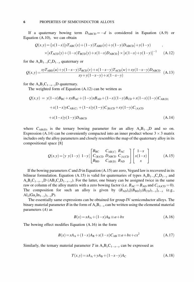
where CAB(D) is the ternary bowing parameter for an alloy AxB1�xD and so on.Expression (A.14) can be conveniently compacted into an inner product whose 3� 3 matrixincludes only the alloy parameters and closely resembles the map of the quaternary alloy in itscompositional space [8]
Qðx;yÞ¼ y yð1�yÞ 1�y½ �BBC CABðCÞ BAC
CðBÞCD DABCD CðAÞCDBBD CABðDÞ BAD
24
35
1�xxð1�xÞ
x
24
35 ðA:15Þ
If the bowing parametersC andD in Equation (A.15) are zero, Vegard law is recovered in itsbilinear formulation. Equation (A.15) is valid for quaternaries of types AxB1�xCyD1�y andAxByC1�x�yD (ABxCyD1�x�y). For the latter, one binary can be assigned twice in the sameraw or column of the alloy matrix with a zero bowing factor (i.e. BAC¼BAD and C(A)CD¼ 0).The composition for such an alloy is given by (BAD)x[(BBD)y(BCD)1�y]1�x (e.g.,Alx(GayIn1�y)1�xP).
The essentially same expressions can be obtained for group-IV semiconductor alloys. Thebinary material parameter B in the form of AxB1�x can be written using the elemental materialparameters (A) as
BðxÞ¼xAAþð1�xÞAB�aþbx ðA:16ÞThe bowing effect modifies Equation (A.16) in the form
BðxÞ¼xAAþð1�xÞABþxð1�xÞCAB�aþbxþcx2 ðA:17Þ
Similarly, the ternary material parameter T in AxByC1�x�y can be expressed as
Tðx;yÞ¼xAAþyABþð1�x�yÞAC ðA:18Þ
6 PROPERTIES OF SEMICONDUCTOR ALLOYS