Embed Size (px)
Citation preview
Journal of Modern OpticsVol. 56, Nos. 2–3, 20 January–10 February 2009, 240–252
Properties of silicon photon counting detectors and silicon photomultipliers
A.G. Stewart, L. Wall and J.C. Jackson*
SensL, Lee House, Riverview Business Park, Blackrock, Cork, Ireland
(Received 28 January 2008; final version received 11 September 2008)
Geiger-mode avalanche photodiodes (APD) or photon counting detectors (PCD) have become the basis ofa range of new detectors and applications. Such devices are sensitive to single photons and are being adaptedto create different detector technologies such as the silicon photomultiplier (SPM). A silicon photomultiplier,so-called because of its similarity in performance to conventional photomultiplier tubes, is based on an arrayof photon counting detectors but with a single common output. While the silicon photomultiplier does notprovide positional information, it does allow photon number resolution and photon counting at higher countrates than are achievable with a solitary PCD. These new detectors are enabling a range of new applications in thefields of medicine, biology, high-energy physics and space exploration. In this paper we report the performance ofPCD with dimensions ranging from 20mm� 20 mm to 200 mm� 200mm and on 1mm2 silicon photomultipliersand illustrate the use of an SPM in single photon counting mode.
Keywords: photon counting; silicon photodetectors; silicon photomultiplier; photomultiplier tube; Geiger-mode;photon timing
1. Introduction
Photon counting detectors (PCD), based on silicon
Geiger-mode avalanche photodiodes (APDs) [1], have
recently come to the market in a range of commercial
products [2] and are used in a diverse range of applica-
tions from the life sciences to astronomy. In theirsimplest form, these detectors make excellent photon
counters with high optical detection efficiency and
fast timing response. However, the photon counting
detectors can also be considered as building blocks
for other detector concepts. For example, by mono-
lithically assembling an N�M array of individually
addressed photon counting detectors, a photon count-
ing camera or DigitalAPD can be realised. Such
a configuration would allow two-dimensional imaging
to be performed under extremely low-light level
conditions [3].Another Geiger-mode photodiode detector array
concept is that of the silicon photomultiplier (SPM)
[4–8]. An SPM detector consists of an array of photon
counting microcells with a single common output.
Each photon counting microcell consists of a Geiger-
mode photodiode in series with a monolithically
integrated quenching element. By connecting all the
SPM microcells in parallel, the SPM can be considered
to be an analogue detector in which the output
photocurrent or number of Geiger pulses is propor-
tional to the number of incident photons. The SPM
detector has many of the attributes of conventionalphotomultiplier tube (PMT) detectors including highgain and single photon sensitivity at room temp-erature. In addition the SPM has all the benefits of asolid-state device such as compactness, high degreeof robustness and low operating bias voltage. The SPMdetector also has two key advantages over the PMT,these are insensitivity to magnetic fields and the SPMis not damaged by exposure to high photon flux.In addition, the SPM offers photon number resolutionwhich is critical for a number of applications includinglinear-optics quantum computing [9]. The SPM isproving useful in a number of applications includingmicroscopy and is particularly suited to the opticalreadout of scintillator crystals and fibres. Scintillatorcrystals and fibres are used to convert high-energyphotons (Gamma and X-ray) and high-energy particlesinto short flashes of lower energy photons with wave-lengths typically in the visible region of the spectrum.Scintillators are widely used in high-energy physicsand nuclear medicine. Positron emission tomography(PET) is a medical imaging technique that producesthree-dimensional images or maps of functional pro-cesses in the body. PET systems rely on the fast andefficient detection of anti-parallel 511 keV gamma raysfrom positron annihilation and SPM detectors areideally suited to the detection of the visible photonsemitted by the scintillator when the gamma raysinteract with the scintillator crystal [10,11].
*Corresponding author. Email: [email protected]
ISSN 0950–0340 print/ISSN 1362–3044 online
� 2009 Taylor & Francis
DOI: 10.1080/09500340802474425
http://www.informaworld.com
2. Silicon photon counting detectors
Planar structure silicon photon counting detectors withwide active areas are required to obtain high photoncollection efficiency without the need for complexand costly optical alignment components and for fibrepigtailing where the fibres typically have diametersof 100 mm. We have fabricated silicon PCD deviceswith a square geometry where the optically sensitiveareas have the dimensions of 10, 20, 50, 100, 150 and200 mm per edge. The devices are fabricated on 100mmdiameter silicon epitaxy on p-type wafers and areformed from planar nþ-p junctions. A selectivelyimplanted region forms an enrichment area thatdefines the optically active area and determines thebreakdown voltage of the device. The polysilicon nþ
top contact layer is formed by diffusion from aphosphorous implant. The nþ layer extends beyondthe enrichment region to form a guard ring. This helpsto reduce the electric field at the edge of the diodeand gives a uniform breakdown [12]. The process alsoprovides for high value, compact resistors which areused for passive quenching circuits where required forPCD and SPM.
Both PCD and SPM devices are characterised onwafer for pre-breakdown leakage current, breakdownvoltage and dark count rate. This is achieved usingan automated wafer probe station from Cascade andcomputer controlled test equipment. The data is usedto create a wafer map that can be used to locate theposition of the best performing detectors. Once thewafer is sawn, the individual silicon die are auto-matically picked and assembled.
2.1. Breakdown voltage
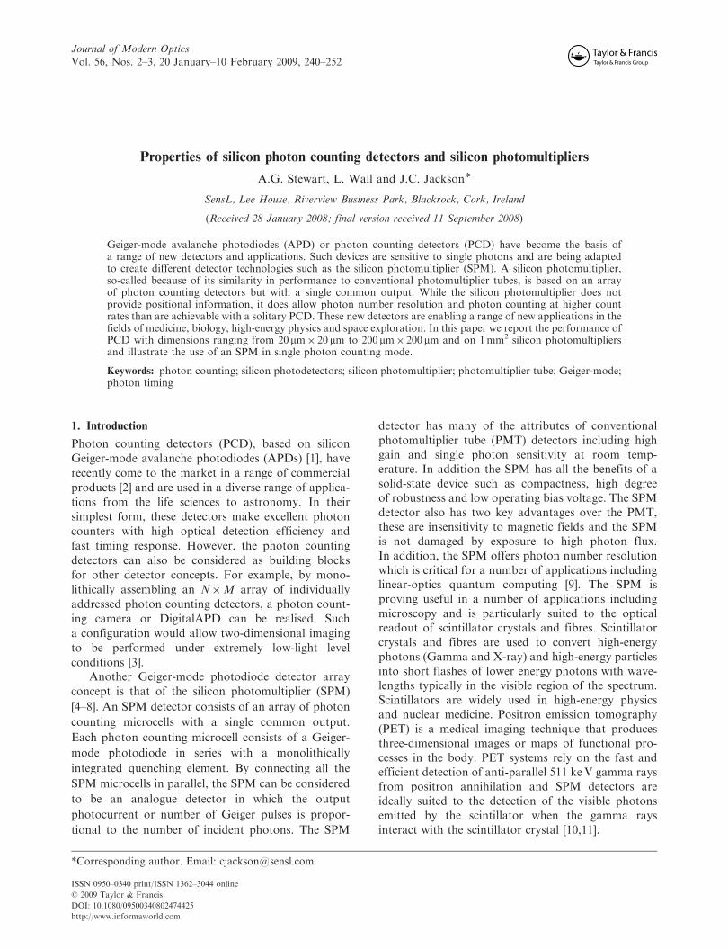
The breakdown voltage of the devices is set by thedopant concentration on the low-doped side of the p-njunction. The uniformity in breakdown voltage acrossa wafer is therefore a good indicator of the processuniformity and is critical in the development of theSPM detectors since variation in the breakdownvoltage across the array of microcells would resultin variations in optical detection efficiency and gain.Figure 1(a) shows the room temperature breakdownvoltage statistics for a total of 420 PCDdevices with active areas of 50 mm� 50 mm and100 mm� 100 mm. The figure shows a histogram ofthe breakdown voltages together with a cumulativeprobability plot. The data shows that 90% of the PCDdevices on the wafer have a breakdown voltagebetween 27.8 and 28V and that 40% of the deviceshave a breakdown voltage of 27.9V. The extremelytight breakdown voltage distribution across the waferis crucial for the development of silicon
photomultipliers and results from the detector design
and the uniformity afforded by modern batch pro-cessed semiconductor fabrication.
2.2. Dark count rate
The dark count rate of the photon counting detectorsis assessed at wafer level as a function of bias voltage
and temperature. The bias voltage is typicallyexpressed as the bias voltage applied in excess ofthe breakdown voltage and is referred to as theoverbias. Since the breakdown voltage is a function oftemperature [13] the same bias voltage at different
temperatures results in different overbias values. Assuch the breakdown voltage should be determinedat different temperatures in order to determine theoverbias. On production wafers all the devices on theentire wafer are measured and the results used to
create a statistical analysis of the wafer dark countrate level as well as allowing individual detectors to bebinned and sorted for assembly. Figure 1(b) showsa cumulative probability plot of the dark count ratedata obtained for all 150mm� 150 mm and all
200 mm� 200 mm PCD devices on a 100mm wafer.The dark count rate was measured at 4V above thebreakdown voltage and at �20�C. The figure showsthat the typical median dark count value fora 150 mm� 150 mm PCD device at 4V above the
breakdown voltage and at �20�C is 5.9 kcps while themedian dark count rate for a 200 mm� 200 mm PCDdevice under identical conditions is 10.3 kcps. Suchprobability plots are used to bin the detectorsaccording to dark count rate. The ratio of the
median dark count rates of the detectors is 0.57while the ratio of the active areas is 0.56; showingthat the dark count rate scales with the area of thedevice.
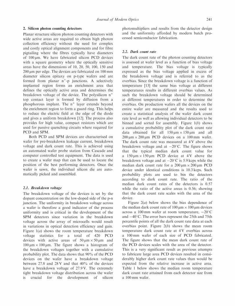
Figure 2(a) below shows the bias dependence ofthe median dark count rate of 100 mm� 100 mm devices
across a 100mm wafer at room temperature, �20�Cand �40�C. The error bars represent the 25th and 75thpercentile points of all the dark count rate data at eachoverbias point. Figure 2(b) shows the mean roomtemperature dark count rate at 4V overbias across
a 100mm wafer of each size of PCD fabricated.The figure shows that the mean dark count rate ofthe PCD devices scales with the area of the detector.This is a very significant result as previous attemptsto fabricate large area PCD devices resulted in consi-
derably higher dark count rate values than would beexpected from the relative increase in active area.Table 1 below shows the median room temperaturedark count rate attained from each detector size froma 100mm wafer.
Journal of Modern Optics 241
2.3. Photon detection probability
The PCD devices are mounted on thermoelectric
coolers (TEC) and housed in hermetically sealed
T08 cans. When the detectors have been packaged
the optical efficiency and spectral response of the
detectors is measured. The photon detection prob-ability (PDP) is given by the quantum efficiency of
silicon, which is a function of wavelength, and the
carrier avalanche initiation probability. The PDP can
be written as
PDPð�,VÞ ¼ �ð�Þ � "ðVÞ , ð1Þ
where �(�) is the quantum efficiency at a given wave-
length � and "(V ) is the carrier avalanche initiation
probability and is a function of the applied bias V.
To measure the optical efficiency or PDP of a detector,
the detector is mounted in an integrating sphere and
the optical efficiency measured relative to a calibrated
large-area silicon PIN diode (Newport 1853-C).
The PCD and Newport detector are mounted in
adjacent ports of an integrating sphere and illuminated
with a low-level continuous signal from a Bentham
TMC300 monochromator and white light source
through a third port in the integrating sphere.
Figure 1. (a) Histogram (primary y-axis) and cumulative probability (secondary y-axis) plot of room temperature breakdownvoltage of 50 mm� 50mm and 100 mm� 100 mm PCD devices across a wafer and (b) cumulative plot of the dark count rate acrossa 100mm wafer at 4V above the breakdown voltage and at �20�C for 150 mm� 150mm (circles) and 200 mm� 200mm (squares)photon counting detectors.
242 A.G. Stewart et al.
The PCD is passively quenched and the signal level
adjusted such that the detected photon rate is typically
less than 100 kHz. The PCD dark count and signal
count rates are then recorded at each wavelength
together with the photon flux as measured by the
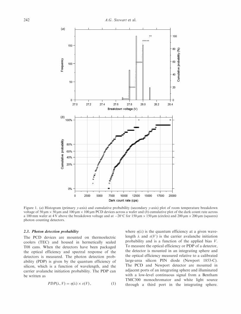
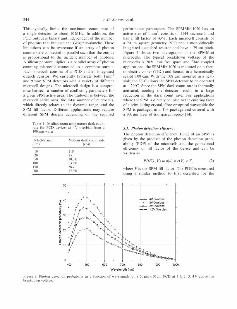
Newport reference detector. Figure 3 shows the PDP
as a function of wavelength of a 50 mm� 50 mmPCD detector at room temperature at 1.5, 2, 3 and
4V above the breakdown voltage. The detectors have
a peak PDP of 42% at 480 nm and at 4V above
breakdown.
3. Silicon photomultipliers
One limitation of photon counting detectors is the
need to quench and reset after every detected photon.
Figure 2. (a) Median dark count rate of 100 mm� 100 mm photon counting detectors as a function of overbias across 100mmwafer at room temperature, �20�C and �40�C and (b) median room temperature dark count rate at 4V overbias as a function ofPCD device area. (The colour version of this figure is included in the online version of the journal.)
Journal of Modern Optics 243
This typically limits the maximum count rate of
a single detector to about 10MHz. In addition, the
PCD output is binary and independent of the number
of photons that initiated the Geiger avalanche. These
limitations can be overcome if an array of photon
counters are connected in parallel such that the output
is proportional to the incident number of photons.
A silicon photomultiplier is a parallel array of photon
counting microcells connected to a common output.
Each microcell consists of a PCD and an integrated
quench resistor. We currently fabricate both 1mm2
and 9mm2 SPM detectors with a variety of different
microcell designs. The microcell design is a compro-
mise between a number of conflicting parameters for
a given SPM active area. The trade-off is between the
microcell active area, the total number of microcells,
which directly relates to the dynamic range, and the
SPM fill factor. Different applications may require
different SPM designs depending on the required
performance parameters. The SPMMini1020 has an
active area of 1mm2, consists of 1144 microcells and
has a fill factor of 43%. Each microcell consists of
a 20 mm square geometry PCD and a monolithically
integrated quenched resistor and have a 29 mm pitch.
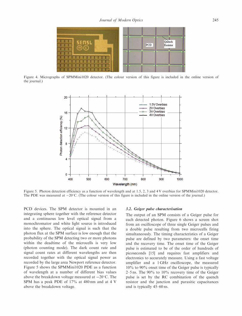
Figure 4 shows two micrographs of the SPMMini
microcells. The typical breakdown voltage of the
microcells is 28V. For free space and fibre coupled
applications, the SPMMini1020 is mounted on a ther-
moelectric cooler (TEC) and housed in a hermetically
sealed T08 can. With the T08 can mounted in a heat-
sink, the TEC allows the SPM detector to be operated
at �20�C. Since the SPM dark count rate is thermally
activated, cooling the detector results in a large
reduction in the dark count rate. For applications
where the SPM is directly coupled to the emitting facet
of a scintillating crystal, fibre or optical waveguide the
SPM is packaged in a T05 package and covered with
a 300 mm layer of transparent epoxy [14].
3.1. Photon detection efficiency
The photon detection efficiency (PDE) of an SPM is
given by the product of the photon detection prob-
ability (PDP) of the microcells and the geometrical
efficiency or fill factor of the device and can be
written as
PDEð�,VÞ ¼ �ð�Þ � "ðVÞ � F , ð2Þ
where F is the SPM fill factor. The PDE is measured
using a similar method to that described for the
Figure 3. Photon detection probability as a function of wavelength for a 50 mm� 50 mm PCD at 1.5, 2, 3, 4V above thebreakdown voltage.
Table 1. Median room temperature dark countrate for PCD devices at 4V overbias from a100mm wafer.
Detector size Median dark count rate(mm) (cps)
10 11020 1 k50 10.3 k100 23.9 k150 58 k200 77.9 k
244 A.G. Stewart et al.
PCD devices. The SPM detector is mounted in an
integrating sphere together with the reference detector
and a continuous low level optical signal from a
monochromator and white light source is introduced
into the sphere. The optical signal is such that the
photon flux at the SPM surface is low enough that the
probability of the SPM detecting two or more photons
within the deadtime of the microcells is very low
(photon counting mode). The dark count rate and
signal count rates at different wavelengths are then
recorded together with the optical signal power as
recorded by the large area Newport reference detector.
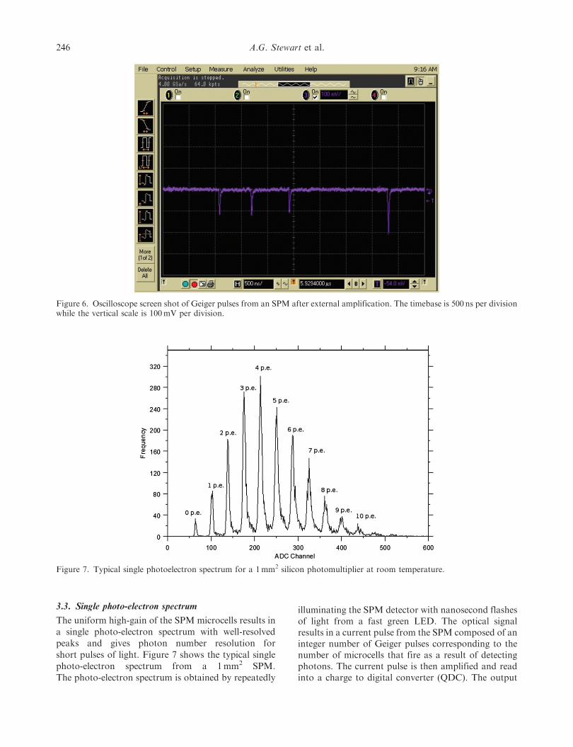
Figure 5 shows the SPMMini1020 PDE as a function
of wavelength at a number of different bias values
above the breakdown voltage measured at �20�C. The
SPM has a peak PDE of 17% at 480 nm and at 4 V
above the breakdown voltage.
3.2. Geiger pulse characterisation
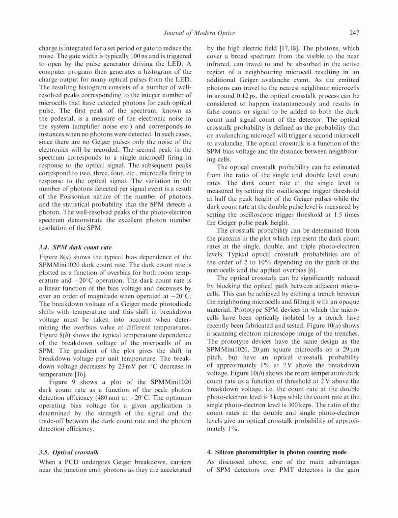
The output of an SPM consists of a Geiger pulse foreach detected photon. Figure 6 shows a screen shotfrom an oscilloscope of three single Geiger pulses anda double pulse resulting from two microcells firingsimultaneously. The timing characteristics of a Geigerpulse are defined by two parameters: the onset timeand the recovery time. The onset time of the Geigerpulse is estimated to be of the order of hundreds ofpicoseconds [15] and requires fast amplifiers andelectronics to accurately measure. Using a fast voltageamplifier and a 1GHz oscilloscope, the measured10% to 90% onset time of the Geiger pulse is typically2–5 ns. The 90% to 10% recovery time of the Geigerpulse is set by the RC combination of the quenchresistor and the junction and parasitic capacitancesand is typically 45–60 ns.
Figure 5. Photon detection efficiency as a function of wavelength and at 1.5, 2, 3 and 4V overbias for SPMMini1020 detector.The PDE was measured at �20�C. (The colour version of this figure is included in the online version of the journal.)
Figure 4. Micrographs of SPMMini1020 detector. (The colour version of this figure is included in the online version ofthe journal.)
Journal of Modern Optics 245
3.3. Single photo-electron spectrum
The uniform high-gain of the SPM microcells results ina single photo-electron spectrum with well-resolvedpeaks and gives photon number resolution for
short pulses of light. Figure 7 shows the typical singlephoto-electron spectrum from a 1mm2 SPM.
The photo-electron spectrum is obtained by repeatedly
illuminating the SPM detector with nanosecond flashesof light from a fast green LED. The optical signalresults in a current pulse from the SPM composed of aninteger number of Geiger pulses corresponding to thenumber of microcells that fire as a result of detectingphotons. The current pulse is then amplified and readinto a charge to digital converter (QDC). The output
Figure 6. Oscilloscope screen shot of Geiger pulses from an SPM after external amplification. The timebase is 500 ns per divisionwhile the vertical scale is 100mV per division.
Figure 7. Typical single photoelectron spectrum for a 1mm2 silicon photomultiplier at room temperature.
246 A.G. Stewart et al.
charge is integrated for a set period or gate to reduce thenoise. The gate width is typically 100 ns and is triggeredto open by the pulse generator driving the LED. Acomputer program then generates a histogram of thecharge output for many optical pulses from the LED.The resulting histogram consists of a number of well-resolved peaks corresponding to the integer number ofmicrocells that have detected photons for each opticalpulse. The first peak of the spectrum, known asthe pedestal, is a measure of the electronic noise inthe system (amplifier noise etc.) and corresponds toinstances when no photons were detected. In such cases,since there are no Geiger pulses only the noise of theelectronics will be recorded. The second peak in thespectrum corresponds to a single microcell firing inresponse to the optical signal. The subsequent peakscorrespond to two, three, four, etc., microcells firing inresponse to the optical signal. The variation in thenumber of photons detected per signal event is a resultof the Poissonian nature of the number of photonsand the statistical probability that the SPM detects aphoton. The well-resolved peaks of the photo-electronspectrum demonstrate the excellent photon numberresolution of the SPM.
3.4. SPM dark count rate
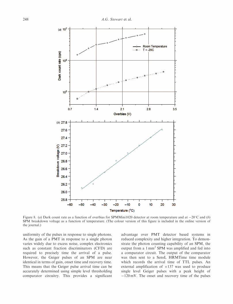
Figure 8(a) shows the typical bias dependence of theSPMMini1020 dark count rate. The dark count rate isplotted as a function of overbias for both room temp-erature and �20�C operation. The dark count rate isa linear function of the bias voltage and decreases byover an order of magnitude when operated at �20�C.The breakdown voltage of a Geiger mode photodiodeshifts with temperature and this shift in breakdownvoltage must be taken into account when deter-mining the overbias value at different temperatures.Figure 8(b) shows the typical temperature dependenceof the breakdown voltage of the microcells of anSPM. The gradient of the plot gives the shift inbreakdown voltage per unit temperature. The break-down voltage decreases by 23mV per �C decrease intemperature [16].
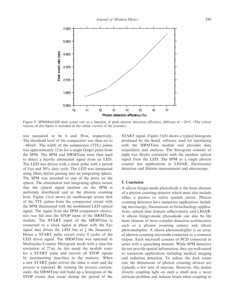
Figure 9 shows a plot of the SPMMini1020dark count rate as a function of the peak photondetection efficiency (480 nm) at �20�C. The optimumoperating bias voltage for a given application isdetermined by the strength of the signal and thetrade-off between the dark count rate and the photondetection efficiency.
3.5. Optical crosstalk
When a PCD undergoes Geiger breakdown, carriersnear the junction emit photons as they are accelerated
by the high electric field [17,18]. The photons, which
cover a broad spectrum from the visible to the nearinfrared, can travel to and be absorbed in the active
region of a neighbouring microcell resulting in anadditional Geiger avalanche event. As the emittedphotons can travel to the nearest neighbour microcells
in around 0.12 ps, the optical crosstalk process can beconsidered to happen instantaneously and results infalse counts or signal to be added to both the dark
count and signal count of the detector. The opticalcrosstalk probability is defined as the probability thatan avalanching microcell will trigger a second microcell
to avalanche. The optical crosstalk is a function of theSPM bias voltage and the distance between neighbour-ing cells.
The optical crosstalk probability can be estimated
from the ratio of the single and double level countrates. The dark count rate at the single level ismeasured by setting the oscilloscope trigger threshold
at half the peak height of the Geiger pulses while thedark count rate at the double pulse level is measured bysetting the oscilloscope trigger threshold at 1.5 times
the Geiger pulse peak height.The crosstalk probability can be determined from
the plateaus in the plot which represent the dark countrates at the single, double, and triple photo-electron
levels. Typical optical crosstalk probabilities are ofthe order of 2 to 10% depending on the pitch of themicrocells and the applied overbias [6].
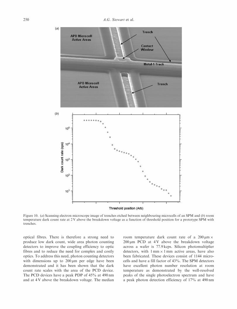
The optical crosstalk can be significantly reduced
by blocking the optical path between adjacent micro-cells. This can be achieved by etching a trench betweenthe neighboring microcells and filling it with an opaque
material. Prototype SPM devices in which the micro-cells have been optically isolated by a trench haverecently been fabricated and tested. Figure 10(a) shows
a scanning electron microscope image of the trenches.The prototype devices have the same design as theSPMMini1020, 20 mm square microcells on a 29 mmpitch, but have an optical crosstalk probabilityof approximately 1% at 2V above the breakdownvoltage. Figure 10(b) shows the room temperature dark
count rate as a function of threshold at 2V above thebreakdown voltage, i.e. the count rate at the doublephoto-electron level is 3 kcps while the count rate at the
single photo-electron level is 300 kcps. The ratio of thecount rates at the double and single photo-electron
levels give an optical crosstalk probability of approxi-mately 1%.
4. Silicon photomultiplier in photon counting mode
As discussed above, one of the main advantagesof SPM detectors over PMT detectors is the gain
Journal of Modern Optics 247
uniformity of the pulses in response to single photons.As the gain of a PMT in response to a single photonvaries widely due to excess noise, complex electronicssuch as constant fraction discriminators (CFD) arerequired to precisely time the arrival of a pulse.However, the Geiger pulses of an SPM are nearidentical in terms of gain, onset time and recovery time.This means that the Geiger pulse arrival time can beaccurately determined using simple level thresholdingcomparator circuitry. This provides a significant
advantage over PMT detector based systems inreduced complexity and higher integration. To demon-strate the photon counting capability of an SPM, theoutput from a 1mm2 SPM was amplified and fed intoa comparator circuit. The output of the comparatorwas then sent to a SensL HRMTime time modulewhich records the arrival time of TTL pulses. Anexternal amplification of �137 was used to producesingle level Geiger pulses with a peak height of�120mV. The onset and recovery time of the pulses
Figure 8. (a) Dark count rate as a function of overbias for SPMMini1020 detector at room temperature and at �20�C and (b)SPM breakdown voltage as a function of temperature. (The colour version of this figure is included in the online version ofthe journal.)
248 A.G. Stewart et al.
was measured to be 6 and 30 ns, respectively.
The threshold level of the comparator was then set to
�60mV. The width of the comparator (TTL) pulses
was approximately 12 ns for a single Geiger pulse from
the SPM. The SPM and HRMTime were then used
to detect a heavily attenuated signal from an LED.
The LED was driven with a clock pulse with a period
of 8 ms and 50% duty cycle. The LED was attenuated
using filters before passing into an integrating sphere.
The SPM was attached to one of the ports on the
sphere. The attenuation and integrating sphere ensure
that the optical signal incident on the SPM is
uniformly distributed and at the photon counting
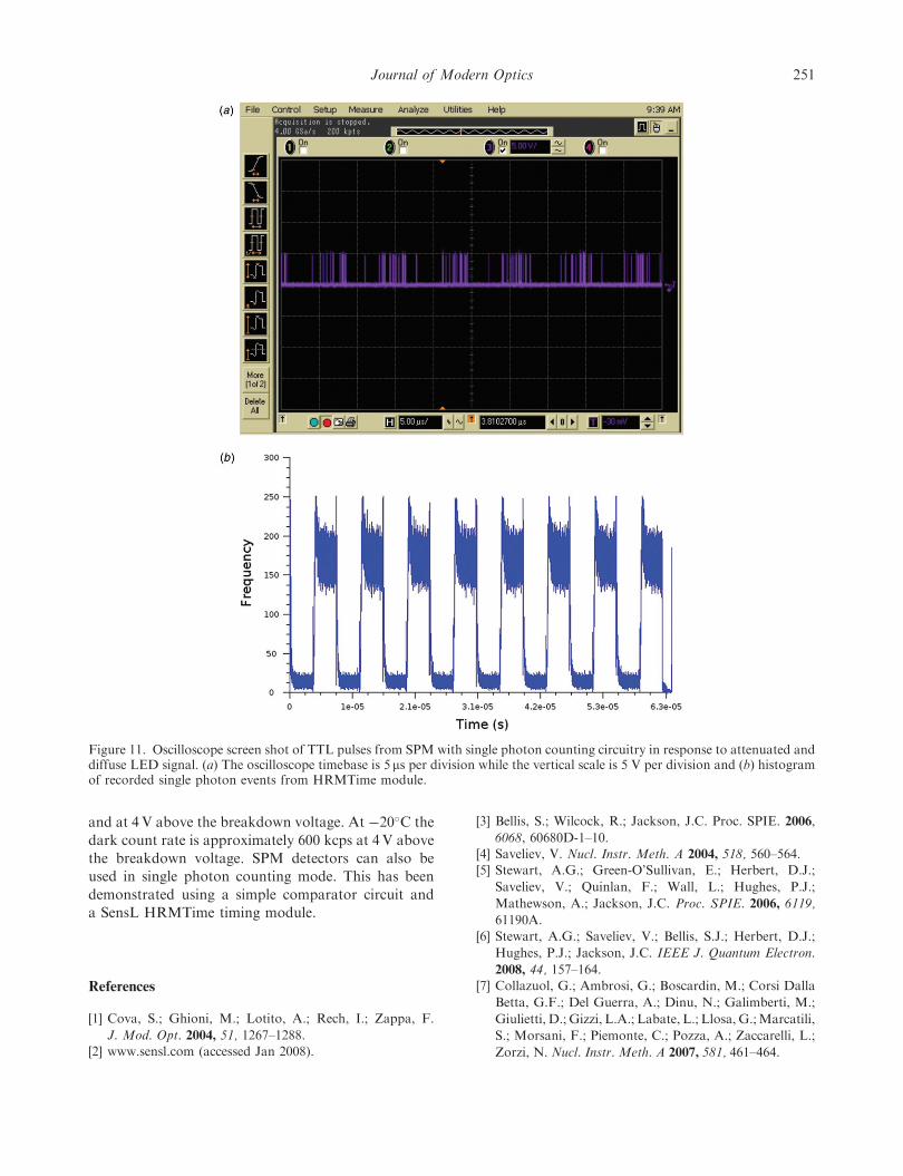
level. Figure 11(a) shows an oscilloscope screen shot
of the TTL pulses from the comparator circuit with
the SPM illuminated with the modulated LED optical
signal. The signal from the SPM comparator electro-
nics was fed into the STOP input of the HRMTime
module. The START input of the HRMTime is
connected to a clock signal in phase with the 8 mssignal that drives the LED but at 1
8 the frequency.
Hence a START pulse occurs every 8 cycles of the
LED driver signal. The HRMTime was operated in
Multiscalar/Counter Histogram mode with a time-bin
resolution of 27 ps. In this mode the module waits
for a START pulse and records all STOP signals
by incrementing time-bins in the memory. When
a new START pulse arrives the timer is reset and the
process is repeated. By running the process continu-
ously, the HRMTime will build up a histogram of the
STOP events that occur during the period of the
START signal. Figure 11(b) shows a typical histogramproduced by the SensL software used for interfacingwith the HRMTime module and provides dataacquisition and analysis. The histogram consists ofeight 4 ms blocks consistent with the incident opticalsignal from the LED. The SPM as a single photoncounter has applications in LIDAR, fluorescencedetection and lifetime measurement and microscopy.
5. Conclusion
A silicon Geiger-mode photodiode is the basic elementof a photon counting detector which must also includeeither a passive or active quench circuit. Photoncounting detectors have numerous applications includ-ing microscopy, fluorescence in biotechnology applica-tions, optical time domain reflectometry and LIDAR.A silicon Geiger-mode photodiode can also be thebasic element of more complex detection architecturessuch as a photon counting camera and siliconphotomultiplier. A silicon photomultiplier is an arrayof photon counting microcells connected to a commonoutput. Each microcell consists of PCD connected inseries with a quenching element. While SPM detectorsdo not provide spatial information, they are well-suitedto numerous applications including medical imagingand radiation detection. To reduce the dark countrate the dimensions of photon counting devices aretypically a few tens of microns. However, this makesdirectly coupling light on such a small area a moreintricate problem and induces losses when coupling to
Figure 9. SPMMini1020 dark count rate as a function of peak photon detection efficiency (480 nm) at �20�C. (The colourversion of this figure is included in the online version of the journal.)
Journal of Modern Optics 249
optical fibres. There is therefore a strong need to
produce low dark count, wide area photon counting
detectors to improve the coupling efficiency to optic
fibres and to reduce the need for complex and costly
optics. To address this need, photon counting detectors
with dimensions up to 200 mm per edge have been
demonstrated and it has been shown that the dark
count rate scales with the area of the PCD device.
The PCD devices have a peak PDP of 45% at 490 nm
and at 4V above the breakdown voltage. The median
room temperature dark count rate of a 200mm�200 mm PCD at 4V above the breakdown voltage
across a wafer is 77.9 kcps. Silicon photomultiplier
detectors, with 1mm� 1mm active areas, have also
been fabricated. These devices consist of 1144 micro-
cells and have a fill factor of 43%. The SPM detectors
have excellent photon number resolution at room
temperature as demonstrated by the well-resolved
peaks of the single photoelectron spectrum and have
a peak photon detection efficiency of 17% at 490 nm
Figure 10. (a) Scanning electron microscope image of trenches etched between neighbouring microcells of an SPM and (b) roomtemperature dark count rate at 2V above the breakdown voltage as a function of threshold position for a prototype SPM withtrenches.
250 A.G. Stewart et al.
and at 4V above the breakdown voltage. At �20�C the
dark count rate is approximately 600 kcps at 4V above
the breakdown voltage. SPM detectors can also be
used in single photon counting mode. This has been
demonstrated using a simple comparator circuit and
a SensL HRMTime timing module.
References
[1] Cova, S.; Ghioni, M.; Lotito, A.; Rech, I.; Zappa, F.
J. Mod. Opt. 2004, 51, 1267–1288.[2] www.sensl.com (accessed Jan 2008).
[3] Bellis, S.; Wilcock, R.; Jackson, J.C. Proc. SPIE. 2006,
6068, 60680D-1–10.[4] Saveliev, V. Nucl. Instr. Meth. A 2004, 518, 560–564.[5] Stewart, A.G.; Green-O’Sullivan, E.; Herbert, D.J.;
Saveliev, V.; Quinlan, F.; Wall, L.; Hughes, P.J.;
Mathewson, A.; Jackson, J.C. Proc. SPIE. 2006, 6119,
61190A.
[6] Stewart, A.G.; Saveliev, V.; Bellis, S.J.; Herbert, D.J.;
Hughes, P.J.; Jackson, J.C. IEEE J. Quantum Electron.
2008, 44, 157–164.[7] Collazuol, G.; Ambrosi, G.; Boscardin, M.; Corsi Dalla
Betta, G.F.; Del Guerra, A.; Dinu, N.; Galimberti, M.;
Giulietti, D.; Gizzi, L.A.; Labate, L.; Llosa, G.;Marcatili,
S.; Morsani, F.; Piemonte, C.; Pozza, A.; Zaccarelli, L.;
Zorzi, N. Nucl. Instr. Meth. A 2007, 581, 461–464.
Figure 11. Oscilloscope screen shot of TTL pulses from SPM with single photon counting circuitry in response to attenuated anddiffuse LED signal. (a) The oscilloscope timebase is 5ms per division while the vertical scale is 5 V per division and (b) histogramof recorded single photon events from HRMTime module.
Journal of Modern Optics 251
[8] Gomi, S.; Hano, H.; Iijima, T.; Itoh, S.; Kawagoe, K.;Kim, S.H.; Kubota, T.; Maeda, T.; Matsumura, T.;
Mazuka, Y.; Miyabayashi, K.; Miyata, H.; Murakami,T.; Nakadaira, T.; Nakaya, T.; Otono, H.; Sano, E.;Shinkawa, T.; Sudo, Y.; Takeshita, T.; Taguchi, M.;Tsubokawa, T.; Uozumi, S.; Yamaoka, M.; Yamazaki,
H.; Yokoyama, M.; Yoshimura, K.; Yoshioka, T. Nucl.Instr. Meth. A 2007, 581, 427–432.
[9] Knill, E.; Laflamme, R.; Milburn, G.J. Nature 2001,
409, 46–52.[10] McElroy, D.P.; Saveliev, V.; Reznik, A.; Rowlands, J.A.
Nucl. Instr. Meth. A 2007, 571, 106–109.
[11] Herbert, D.J.; Stewart, A.G.; Hughes, P.J.; Jackson, J.C.IEEE Nuclear Science Symposium and Medical ImagingConference (NSS-MIC 2007).
[12] Jackson, J.C.; Morrison, A.P.; Phelan, D.;Mathewson, A. IEEE International Electron Devices
Meeting 2002, 32, 797–800.[13] Sze, S.M. Physics of Semiconductor Devices, 2nd ed.;
Wiley-Interscience: New York, 1981; pp. 105–106.[14] SPMScint1020 Datasheet, 2007. www.sensl.com
(accessed Jan 2008).[15] Kovaltchouk, D.V.; Lolos, G.J.; Papandreou, Z.;
Wolbaum, K. Nulc. Instr. Meth. A 2005, 538, 408–415.
[16] Goetzberger, A.; McDonald, B.; Haitz, R.H.; Scarlet,R.M. J. Appl. Phys. 1963, 34, 1591–1600.
[17] Jackson, J.C.; Morrison, A.P.; Phelan, D.; Mathewson,
A. IEEE Trans. Electron Devices. 2002, 32, 797–800.[18] Akil, N. IEEE Trans. Electron Devices. 1999, 46,
1022–1028.
252 A.G. Stewart et al.