Embed Size (px)
Citation preview
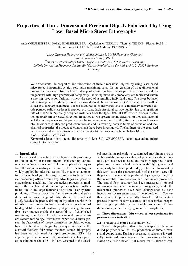
JLMN-Journal of Laser Micro/Nanoengineering Vol. 3, No. 2, 2008
Properties of Three-Dimensional Precision Objects Fabricated by Using Laser Based Micro Stereo Lithography
Andre NEUMEISTER*, Roland HIMMELHUBER**, Christian MATERLIK*, Thorsten TEMME*, Florian PAPE***, Hans-Heinrich GATZEN***, and Andreas OSTENDORF*
*Laser Zentrum Hannover e.V., Hollerithallee 8, 30419 Hannover, Germany E-mail: [email protected]
**micro resist technology GmbH, Köpenicker Str. 325, 12555 Berlin, Germany ***Leibniz Universität Hannover, Institut für Mikrotechnologie, An der Universität 2, 30823 Garbsen,
Germany
We demonstrate the properties and fabrication of three-dimensional objects by using laser based mico stereo lithography. A high resolution machining setup for the creation of three-dimensional precision components from a UV-curable photo-resin has been developed. Micro-mechanical ar-rangements with high geometrical complexity, including movable components are fabricated within a one step production fashion, without the need of assembling individual parts. The layer-by-layer fabrication process is directly based on a user defined, three-dimensional CAD model which will be sliced at a constant increment. For the illumination of individual layers, a frequency-converted di-ode-pumped solid-state laser is applied, providing high structural surface quality due to a repetition rate of 100 MHz. Specially designed materials from the type ORMOCER® offer a process resolu-tion up to 20 µm in vertical direction. In particular, we present the modification of the resin material and the consequences on the process resolution to achieve the suitability for micro stereo lithogra-phy. In order to qualify the production process and its resulting parts in terms of precision and me-chanical properties, the produced components have been investigated. The hardness of the generated parts has been determined to more than 1 GPa at a lateral process resolution below 10 µm.
Keywords: laser micro stereo lithography (micro SL), ORMOCER®, nano indentation, micro computer tomography
1. Introduction Laser based production technologies with processing
resolutions down to the sub-micron level open up various new technology sectors and fields of applications. Apart from the use in laboratory environment, laser technology is widely applied in industrial sectors like medicine, automo-tive or biotechnology. The usage of lasers as tools in mate-rial processing offers diverse key advantages compared to conventional machining: the contactless processing mini-mizes the mechanical stress during production. Further-more, due to the large number of available laser systems providing different properties (i.e. wavelength and pulse duration), a broad range of materials can be machined [1, 2]. Besides the precise drilling of injection nozzles with ultrashort laser pulses, high-quality stents are made out of biodegradable materials without post-processing. Innova-tive laser sources enable the accessibility of established machining technologies from the macro scale towards mi-cro system technology. Within this paper, the authors pre-sent the fabrication of three-dimensional precision objects, based on the stereo lithography principle. As one of the classical freeform fabrication methods, stereo lithography has been basically used for rapid prototyping (RP). The applied optical equipment in RP machines enables a proc-ess resolution of about 75 – 150 µm. Oriented at the classi-
cal machining principle, a customized machining system with a suitable setup for enhanced process resolution down to 10 µm has been released and recently reported. Exem-plary, micro mechanical devices with high geometrical complexity have been produced [3]. The main focus within this work is on the characterisation of the micro stereo li-thography process and the produced objects, regarding both the achievable form accuracy and mechanical properties. The spatial form accuracy has been measured by optical microscopy and micro computer tomography, while the mechanical properties have been distinguished by nano indentation measurements and nano scratch tests. The au-thors aim is to provide a fully characterized fabrication process in terms of form accuracy and mechanical proper-ties, being applicable for the reliable production of three dimensional parts with high geometrical complexity.
2. Three dimensional fabrication of test specimens for process characterization
2.1 Principle of stereo lithography (SL) Stereo lithography utilizes the principle of photo in-
duced polymerization for the production of three dimen-sional components. During processing, a substrate is verti-cally positioned inside a resin filled processing chamber. Based on a user-defined CAD model, that is sliced at con-
67
JLMN-Journal of Laser Micro/Nanoengineering Vol. 3, No. 2, 2008
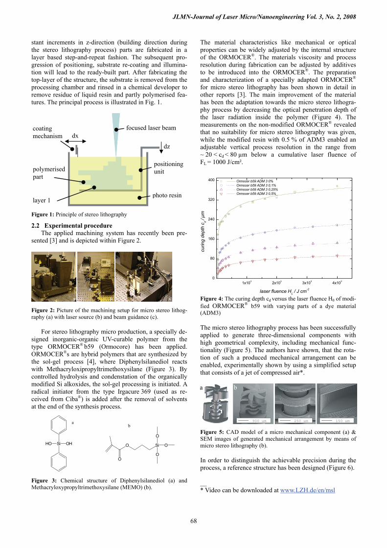
stant increments in z-direction (building direction during the stereo lithography process) parts are fabricated in a layer based step-and-repeat fashion. The subsequent pro-gression of positioning, substrate re-coating and illumina-tion will lead to the ready-built part. After fabricating the top-layer of the structure, the substrate is removed from the processing chamber and rinsed in a chemical developer to remove residue of liquid resin and partly polymerised fea-tures. The principal process is illustrated in Fig. 1.
Figure 1: Principle of stereo lithography
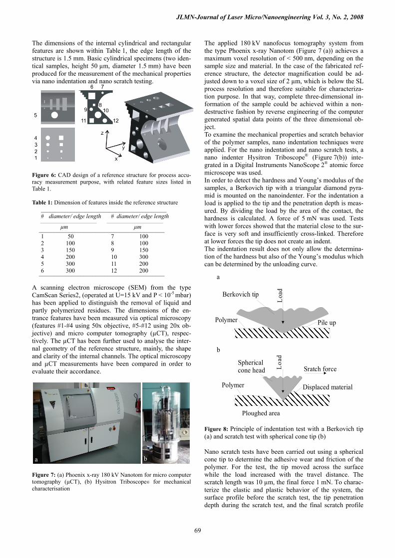
2.2 Experimental procedure The applied machining system has recently been pre-
sented [3] and is depicted within Figure 2.
Figure 2: Picture of the machining setup for micro stereo lithog-raphy (a) with laser source (b) and beam guidance (c).
For stereo lithography micro production, a specially de-signed inorganic-organic UV-curable polymer from the type ORMOCER® b59 (Ormocore) has been applied. ORMOCER®s are hybrid polymers that are synthesized by the sol-gel process [4], where Diphenylsilanediol reacts with Methacryloxipropyltrimethoxysilane (Figure 3). By controlled hydrolysis and condenstation of the organically modified Si alkoxides, the sol-gel processing is initiated. A radical initiator from the type Irgacure 369 (used as re-ceived from Ciba®) is added after the removal of solvents at the end of the synthesis process.
Si OHHO O
O
Si
O
O
O
ab
Figure 3: Chemical structure of Diphenylsilanediol (a) and Methacryloxypropyltrimethoxysilane (MEMO) (b).
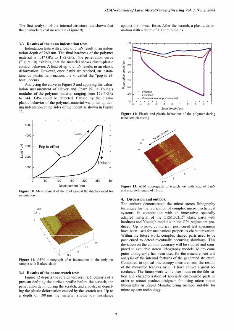
The material characteristics like mechanical or optical properties can be widely adjusted by the internal structure of the ORMOCER®. The materials viscosity and process resolution during fabrication can be adjusted by additives to be introduced into the ORMOCER®. The preparation and characterization of a specially adapted ORMOCER® for micro stereo lithography has been shown in detail in other reports [3]. The main improvement of the material has been the adaptation towards the micro stereo lithogra-phy process by decreasing the optical penetration depth of the laser radiation inside the polymer (Figure 4). The measurements on the non-modified ORMOCER® revealed that no suitability for micro stereo lithography was given, while the modified resin with 0.5 % of ADM3 enabled an adjustable vertical process resolution in the range from ~ 20 < cd < 80 µm below a cumulative laser fluence of FL = 1000 J/cm².
focused laser beamcoating dx mechanism
dz
positioningpolymerised unit part
1x10³ 2x10³ 3x10³ 4x1030
80
160
240
320
400 Ormocer b59 ADM 3 0% Ormocer b59 ADM 3 0,1% Ormocer b59 ADM 3 0,25% Ormocer b59 ADM 3 0,5%
curin
g de
pth
c d / µ
m
laser fluence H0 / J cm-2
Figure 4: The curing depth cd versus the laser fluence H0 of modi-fied ORMOCER® b59 with varying parts of a dye material (ADM3)
photo resinlayer 1
The micro stereo lithography process has been successfully applied to generate three-dimensional components with high geometrical complexity, including mechanical func-tionality (Figure 5). The authors have shown, that the rota-tion of such a produced mechanical arrangement can be enabled, experimentally shown by using a simplified setup that consists of a jet of compressed air*.
a b
900 µm 250 µm 150 µm
Figure 5: CAD model of a micro mechanical component (a) & SEM images of generated mechanical arrangement by means of micro stereo lithography (b). In order to distinguish the achievable precision during the process, a reference structure has been designed (Figure 6). __ * Video can be downloaded at www.LZH.de/en/msl
68
JLMN-Journal of Laser Micro/Nanoengineering Vol. 3, No. 2, 2008
The dimensions of the internal cylindrical and rectangular features are shown within Table 1, the edge length of the structure is 1.5 mm. Basic cylindrical specimens (two iden-tical samples, height 50 µm, diameter 1.5 mm) have been produced for the measurement of the mechanical properties via nano indentation and nano scratch testing.
Figure 6: CAD design of a reference structure for process accu-racy measurement purpose, with related feature sizes listed in Table 1. Table 1: Dimension of features inside the reference structure
__________________________________________ # diameter/ edge length # diameter/ edge length
__________________________________ __________________________________
µm µm __________________________________________ 1 50 7 100 2 100 8 100 3 150 9 150 4 200 10 300 5 300 11 200 6 300 12 200 __________________________________________
A scanning electron microscope (SEM) from the type CamScan Series2, (operated at U=15 kV and P < 10-5 mbar) has been applied to distinguish the removal of liquid and partly polymerized residues. The dimensions of the en-trance features have been measured via optical microscopy (features #1-#4 using 50x objective, #5-#12 using 20x ob-jective) and micro computer tomography (µCT), respec-tively. The µCT has been further used to analyse the inter-nal geometry of the reference structure, mainly, the shape and clarity of the internal channels. The optical microscopy and µCT measurements have been compared in order to evaluate their accordance.
Figure 7: (a) Phoenix x-ray 180 kV Nanotom for micro computer tomography (µCT), (b) Hysitron Triboscope® for mechanical characterisation
The applied 180 kV nanofocus tomography system from the type Phoenix x-ray Nanotom (Figure 7 (a)) achieves a maximum voxel resolution of < 500 nm, depending on the sample size and material. In the case of the fabricated ref-erence structure, the detector magnification could be ad-justed down to a voxel size of 2 µm, which is below the SL process resolution and therefore suitable for characteriza-tion purpose. In that way, complete three-dimensional in-formation of the sample could be achieved within a non-destructive fashion by reverse engineering of the computer generated spatial data points of the three dimensional ob-ject. To examine the mechanical properties and scratch behavior of the polymer samples, nano indentation techniques were applied. For the nano indentation and nano scratch tests, a nano indenter Hysitron Triboscope® (Figure 7(b)) inte-grated in a Digital Instruments NanoScope 2® atomic force microscope was used. In order to detect the hardness and Young’s modulus of the samples, a Berkovich tip with a triangular diamond pyra-mid is mounted on the nanoindenter. For the indentation a load is applied to the tip and the penetration depth is meas-ured. By dividing the load by the area of the contact, the hardness is calculated. A force of 5 mN was used. Tests with lower forces showed that the material close to the sur-face is very soft and insufficiently cross-linked. Therefore at lower forces the tip does not create an indent. The indentation result does not only allow the determina-tion of the hardness but also of the Young’s modulus which can be determined by the unloading curve.
LoadBerkovich tip
Sratch force
Displaced material
Load
Phlouged Area
Polymer Pile up
Spherical cone head
a
b
Polymer
Ploughed area
Figure 8: Principle of indentation test with a Berkovich tip (a) and scratch test with spherical cone tip (b) Nano scratch tests have been carried out using a spherical cone tip to determine the adhesive wear and friction of the polymer. For the test, the tip moved across the surface while the load increased with the travel distance. The scratch length was 10 µm, the final force 1 mN. To charac-terize the elastic and plastic behavior of the system, the surface profile before the scratch test, the tip penetration depth during the scratch test, and the final scratch profile
b a
69
JLMN-Journal of Laser Micro/Nanoengineering Vol. 3, No. 2, 2008
after the scratch test were recorded. Figure 8 shows the principle of an indentation and a scratch test. During the indentation test, material is piled up at the edge of the indent. During the scratch test, displaced material accumulates in front of the tip and next to it.
3. Results
3.1 Scanning electron microscopy SEM analyses have shown, that the fabricated structure
is clearly defined and no residues (resin or chemicals due to cleaning) are left on the structures’ surface. Detailed im-ages of the structure are shown within Figure 9.
Figure 9: SEM images of the reference structure, fabricated with a cumulative fluence of FL= 208 Jcm-2
According to the CAD model, all channels have an open, defined entrance. On the top surface of the structure, rec-tangular and circular features down to ~50 µm (edge length and diameter) are visible. The individual layers of the structure can be detected clearly. Optical microscopy and computer tomography are used to further analyze the form accuracy in more detail.
3.2 Optical microscopy and micro computer tomogra-phy
The measurement data generated with optical micros-copy is listed within Table 2; the data generated with micro computer tomography is shown in Table 3, respectively. Table 2: Measured geometry features via optical microscopy ____________________________________________________ # diameter, (deviation)/ m # edge length, (deviation)/ µ _________________ ___________________ µ m
(x-dir.) (y-dir.) (x-dir.) (y-dir.) ____________________________________________________ 1 38 (-12) 38 (-12) 1 44 (-6) 50 (0) 2 89 (-11) 89 (-11) 2 93 (-7) 94 (-6) 3 136 (-14) 136 (-14) 3 139 (-11) 140 (-10) 4 184 (-16) 184 (-16) 4 187 (-13) 194 (-6) _______________________________________________
(x-dir.) (z-dir.) (x-dir.) (z-dir.) ____________________________________________________ 7 90 (-10) 67 (-33) 8 91 (-9) 51 (-49) 9 137 (-13) 108 (-42) 12 191 (-9) 166 (-34) 11 191 (-9) 166 (-34) 10 278 (-22) 265 (-35) 6 279 (-31) 268 (-32) ____________________________________________________
The measurement of the features #1-#4 shows, that the deviation on the contour accuracy is independent from the size, shape and measurement direction of the generated through hole. Furthermore, the results generated with opti-cal microscopy (Table 2) agree with the results generated by µCT (Table 3) very well. The deviation average is ~ 13 µm, which is in the order of the half of the curing width at the deployed fabrication parameters. Table 3: Measured geometry features via computer tomography ____________________________________________________ diameter, (deviation)/ µm # edge length, (deviation)/ µ _________________ ___________________ # m
(x-dir.) (y-dir.) (x-dir.) (y-dir.) ___________________________________________________ 1 38 (-12) 38 (-12) 1 39 (-11) 44 (-6) 2 88 (-12) 88 (-12) 2 91 (-9) 93 (-7) 3 136 (-14) 136 (-14) 3 139 (-11) 140 (-10) 4 184 (-16) 184 (-16) 4 186 (-14) 190 (-10) _______________________________________________
(x-dir.) (z-dir.) (x-dir.) (z-dir.) ____________________________________________________ 7 82 (-18) 66 (-34) 8 84 (-16) 43 (-57) 9 - - 12 185 (-15) 153 (-47) 11 185 (-15) 153 (-47) 10 - - - - ____________________________________________________ For minimizing this error, the lateral dimension of the laser spot size at structural edges needs to be considered, result-ing in a negative offset do of the laser scanning path at structural edges (do ~ 0.5 curing width cw). Whether any shrinkage occurs during the curing process, and may lead to further inaccuracy, needs to be figured out in more de-tailed experimentation. The deviation of the vertically ar-ranged features (#7–#12) can not simply be interpreted by an offset error, since a distinctive difference between the deviations in x- and y-direction has been detected. While the error in the x-direction is exactly in the order of the previously measured through holes #1-#4, the one in the y-direction is in the range between 32 and 49 µm. The differ-ence is caused by the optical penetration of the laser radia-tion into the liquid resin with subsequently initiated polym-erization. According to Figure 4, the process parameters (cumulative laser fluence FL = 208 Jcm-2 [10.4 mJcm-2 at a hatch distance dh = 0.001 mm]) lead to a curing depth of around cd= 45 µm which is in agreement with the detected deviation. Since the penetration of the optical radiation inside the material is required for layer bonding and suffi-cient cohesion between individual layers, a further reduc-tion of the penetration depth may result in a micro part with poor structural stability.
Figure 9: Vertical cross section images of the internal structure of the demonstrator, generated by means of µCT
220 µm 130 µm 220 µm
130 µm 130 µm 220 µm
70
JLMN-Journal of Laser Micro/Nanoengineering Vol. 3, No. 2, 2008
The first analysis of the internal structure has shown that the channels reveal no residue (Figure 9).
3.3 Results of the nano indentation tests Indentation tests with a load of 5 mN result in an inden-
tation depth of 260 nm. The final hardness of the polymer material is 1.47 GPa to 1.82 GPa. The penetration curve (Figure 10) exhibits, that the material shows elasto-plastic contact behavior. A load of up to 2 mN results in an elastic deformation. However, once 2 mN are reached, an instan-taneous plastic deformation, the so-called the “pop-in ef-fect”, occurs.
Analysing the curve in Figure 3 and applying the calcu-lation measurement of Oliver and Pharr [5], a Young’s modulus of the polymer material ranging from 129.6 GPa to 144.1 GPa could be detected. Caused by the elasto-plastic behavior of the polymer, material was piled up dur-ing indentation at the sides of the indent as shown in Figure 11.
0 50 100 150 200 250 3000
1000
2000
3000
4000
5000
Load
/ µN
Displacement / nm Figure 10: Measurement of the load against the displacement for indentation
0.51.0
1.5µm
0.5µm
0
Figure 11: AFM micrograph after indentation in the polymer sample with Berkovich tip
3.4 Results of the nanoscratch tests Figure 12 depicts the scratch test results. It consists of a
prescan defining the surface profile before the scratch, the penetration depth during the scratch, and a postscan depict-ing the plastic deformation caused by the scratch test. Up to a depth of 180 nm the material shows low resistance
against the normal force. After the scratch, a plastic defor-mation with a depth of 100 nm remains.
-5 -4 -3 -2 -1 0 1 2 3 4 5700
600
500
400
300
200
100
0
-100
Prescan Postscan Penetration during scratch test
Pen
etra
tion
dept
h / n
m
Scan length / µm Figure 12: Elastic and plastic behaviour of the polymer during nano scratch testing
5
10
µm
1.0µm
0
0
-5
µm
Scratch direction
Load
Pop in effect
Unload
Figure 13: AFM micrograph of scratch test with load of 1 mN and a scratch length of 10 µm
4. Discussion and outlook The authors demonstrated the micro stereo lithography technique for the fabrication of complex micro mechanical systems. In combination with an innovative, specially adapted material of the ORMOCER® class, parts with hardness and Young’s modulus in the GPa regime are pro-duced. Up to now, cylindrical, post cured test specimens have been used for mechanical properties characterization. Within the future work, complex shaped parts need to be post cured to detect eventually occurring shrinkage. This deviation on the contour accuracy will be studied and com-pared to available stereo lithography models. Micro com-puter tomography has been used for the measurement and analysis of the internal features of the generated structure. Compared to optical microscopy measurement, the results of the measured features by µCT have shown a great ac-cordance. The future work will closer focus on the fabrica-tion and characterization of specially customized parts in order to attract product designers for using micro stereo lithography as Rapid Manufacturing method suitable for micro system technology.
71
JLMN-Journal of Laser Micro/Nanoengineering Vol. 3, No. 2, 2008
Acknowledgments The authors would like to thank Phoenix x-ray GmbH, Wunstorf (Germany) for micro computer tomography measurements. Parts of the results have been funded by the European commission within the project “Rapid Production Tool for micro mechanical systems (PronTo)”. ORMOCER® is registered trademark of the „Fraunhofer Gesellschaft zur Foerderung der angewandten Forschung in Deutschland e.V.” Triboscope® is registred trademark of Hysitron Incorpo-rated, NanoScope 2® is registred trademark of Digital In-struments.
References [1] H. Rohde, E. Meiners: J. Laser Appl., 8, (1996)
95-101 [2] H.-K. Toenshoff, A. Ostendorf, S. Nolte, F. Korte,
T. Bauer: Proc. of SPIE Vol. 4088, (2000) 136-139 [3] A. Neumeister, R. Himmelhuber, T. Temme, U.
Stute: Proc. of 17th Solid Freeform Fabrication Symposium, Austin (2006) 12-24
[4] R. Buestrich, F. Kahlenberg, M. Popall, P. Dannberg, R. Mueller-Fieldler, O. Roesch: J. of sol-gel science technology, 20, (2001) 181
[5] W.C. Oliver, G.M. Pharr: J. of Materials Research, 7(6), (1992) 1564–1583,
(Received: May 08, 2007, Accepted: January 17, 2008)
72