Embed Size (px)
Citation preview

Dayane do Carmo Mendonça
Proposal of Minimum Cell Operation Control
for Efficiency Improvement in DSCC
MMCC-based STATCOMs
Belo Horizonte, MG
2021


Dayane do Carmo Mendonça
Proposal of Minimum Cell Operation Control for
Efficiency Improvement in DSCC MMCC-based
STATCOMs
Dissertacao submetida a banca examinadora
designada pelo Colegiado do Programa de
Pos-Graduacao em Engenharia Eletrica do
Centro Federal de Educacao Tecnologica de
Minas Gerais e da Universidade Federal de
Sao Joao Del Rei, como parte dos requisitos
necessarios a obtencao do grau de Mestre em
Engenharia Eletrica.
Centro Federal de Educacao Tecnologica de Minas Gerais
Programa de Pos-Graduacao em Engenharia Eletrica
Orientador: Prof. Dr. Heverton Augusto Pereira
Coorientador: Prof. Dr. Allan Fagner Cupertino
Belo Horizonte, MG
2021

Mendonça, Dayane do CarmoM539p Proposal of minimum cell operation control for efficiency
improvement in DSCC MMCC-based STATCOMs / Dayane do CarmoMendonça. – 2021.
119 f.: il., gráfs, tabs.
Dissertação de mestrado apresentada ao Programa de Pós-Graduaçãoem Engenharia Elétrica em associação ampla entre a UFSJ e oCEFET-MG.
Orientador: Heverton Augusto Pereira.Coorientador: Allan Fagner Cupertino.Banca examinadora: Heverton Augusto Pereira, Allan Fagner
Cupertino, Marcelo Martins Stopa e Pedro Gomes Barbosa.Dissertação (mestrado) – Centro Federal de Educação Tecnológica
de Minas Gerais.
1. Conversores de corrente elétrica – Teses. 2. Sistemas de energiaelétrica – Perdas elétricas – Teses. 3. Sistemas elétricos de potência –Controle – Teses. 4. Estabilidade do sistema de energia elétrica – Teses.I. Pereira, Heverton Augusto. II. Cupertino, Allan Fagner. III. CentroFederal de Educação Tecnológica de Minas Gerais. IV. UniversidadeFederal de São João del-Rei. V. Título.
CDD 621.3815322
Elaboração da ficha catalográfica pela bibliotecária Jane Marangon Duarte,CRB 6o 1592 / Cefet/MG

Dayane do Carmo Mendonça
Proposal of Minimum Cell Operation Control for
Efficiency Improvement in DSCC MMCC-based
STATCOMs
Dissertacao submetida a banca examinadora designada pelo Colegiado do Programade Pos-Graduacao em Engenharia Eletrica do Centro Federal de Educacao Tecnologica deMinas Gerais e da Universidade Federal de Sao Joao Del Rei, como parte dos requisitosnecessarios a obtencao do grau de Mestre em Engenharia Eletrica.
Trabalho aprovado em 16 de Abril de 2021.
COMISSAO EXAMINADORA
Prof. Dr. Heverton Augusto Pereira
Orientador
Prof. Dr. Allan Fagner Cupertino
Coorientador
Prof. Dr. Marcelo Martins Stopa
Convidado 1
Prof. Dr. Pedro Gomes Barbosa
Convidado 2
Belo Horizonte, MG
2021


A minha famılia, mentores e amigos.


Agradecimentos
Agradeco primeiramente a Deus pelo dom da vida e por iluminar todos os meus
passos durante esta jornada. Aos meus pais, Odail e Luciana, pelo exemplo de integridade
e carater, pelo amor sem medida, incentivo, compreensao e exemplos de vida. Ao meu
irmao Arlan pela companhia, conselhos e ajuda nos estudos. Ao meu noivo Allan, por
todo o carinho, amor, paciencia e apoio. Aos meus avos, tios, primos e amigos pela torcida.
Aqueles que ja nao estao mais aqui, mas que sempre torceram por mim e continuam
iluminando meu caminho de onde estiverem.
Aos professores que me orientaram neste trabalho, Prof. Heverton e Prof. Allan.
Aos membros do grupo de pesquisa GESEP, por todo companherismo e conhecimento
compartilhado. Por fim, agradeco ao CEFET-MG pelo apoio financeiro.


“Por vezes sentimos que aquilo que fazemos nao e senao uma gota de agua no mar. Mas o
mar seria menor se lhe faltasse uma gota.”
(Madre Teresa de Calcuta)


Resumo
O cenario atual dos sistemas eletricos de potencia e caracterizado por estruturas complexas,
presenca de cargas nao lineares e alta insercao de energias renovaveis, como energia solar
e eolica. Desta forma, o compensador sıncrono estatico (do ingles, Static synchronous
Compensator — STATCOM) surge para regulacao de tensao e controle de potencia reativa
nesses sistemas. Como os STATCOMs sao dispositivos que operam em hot standby, ou
seja, estao sempre conectados a rede, a eficiencia do conversor e muito importante. Nesse
cenario, as topologias de conversores modulares multinıveis em cascata (do ingles, Modular
Multilevel Cascade Converter — MMCC) tem sido usadas para a realizacao do STATCOM
devido a sua alta eficiencia. Para melhorar a eficiencia do STATCOM, diferentes estrategias
tem sido propostas na literatura. No entanto, a maioria das estrategias exigem modificacoes
no hardware. Alem disso, a maioria das propostas que nao exigem modificacao no hardware
tem o potencial apenas de reduzir as perdas de comutacao. No entanto, como o MMCC
geralmente trabalha com frequencias de comutacao na faixa de 100 - 200 Hz, as perdas de
conducao predominam. De fato, poucas estrategias para reduzir as perdas de conducao
foram propostas na literatura. Esta dissertacao de mestrado visa preencher esse vazio. Este
trabalho propoe um controle de operacao com numero mınimo de celulas para reduzir as
perdas de energia no STATCOM com base no MMCC. O princıpio da tecnica e desconectar
celulas do MMCC, de acordo com a referencia de potencia reativa. Para isso, sao derivadas
expressoes analıticas para a tensao mınima do barramento cc para manter a operacao
do conversor na regiao linear do modulador. Essas expressoes sao usadas para calcular
o numero de celulas que podem ser retiradas do conversor para determinadas condicoes
de operacao. Alem disso, o potencial da estrategia proposta para reducao de perdas de
energia e as limitacoes da abordagem sao investigadas. O desempenho dinamico do esquema
proposto e avaliado com base em simulacoes no PLECS de um STATCOM de 17 MVA
e 13,8 kV. Por fim, foi realizado um estudo de economia de energia de um ano para um
perfil de potencia reativa real, que apresentou uma reducao de 7,37 % nas perdas totais
de energia. Os resultados indicaram que essa metodologia e uma solucao inovadora para
reduzir perdas de energia e custos operacionais. A tecnica proposta pode ser aplicada em
STATCOMs baseados em MMCC com mais de 10 celulas por braco e nao requer hardware
adicional.
Palavras-chaves: Conversor Modular Multinıvel em Cascata, Operacao com Numero
Mınimo de Celulas, Perdas de Energia, STATCOM.


Abstract
The current power systems scenario is characterized by complex structures, presence of
nonlinear loads and high penetration of renewable energy such as solar and wind power
plants. Then, the Static synchronous Compensator (STATCOM) emerges to perform
voltage regulation and reactive power control in these power systems. Since STATCOMs
are hot standby devices, the converter efficiency is very important. In this scenario, modular
multilevel cascade converter (MMCC) topologies have been used for STATCOM realization
due to their high efficiency. To further improve the STATCOM efficiency, different strategies
have been proposed in literature. However, most of the strategies require modification in
the hardware. In addition, most proposals that do not require modification to the hardware
have the potential only to reduce switching losses. Nevertheless, since MMCC usually
employs switching frequencies in the range of 100 - 200 Hz, the conduction losses dominate.
Indeed, few strategies to reduce conduction losses have been proposed in the literature.
This Master Thesis aims to fill this void. This work proposes a minimum cell operation
control to reduce power losses in STATCOM based on MMCC. The main principle is
to bypass cells from the MMCC, according to the reactive power reference. For such,
analytical expressions for the minimum dc-link voltage to keep the converter operation in
the modulator linear region are derived. These expressions are used to compute the number
of cells which can be bypassed for given operation conditions. Moreover, the potential
of the proposed strategy for power losses reduction and the limitations of the proposed
approach are investigated. The dynamic performance of the proposed scheme is evaluated
based on simulations in PLECS of a 17 MVA, 13.8 kV STATCOM. Finally, an one-year
energy saving study was conducted for a real reactive power profile, which presented a
7.37 % reduction in the total energy losses. The results indicated that this methodology
is a breakthrough solution to reduce power losses and operational costs. The proposed
technique can be applied in MMCC-based STATCOMs with more than 10 cells per arm
and does not require additional hardware.
Key-words: Modular Multilevel Cascade Converter, Minimum Cell Operation, Power
Losses, STATCOM.


List of Figures
Figure 1 – Reactive power compensators: (a) Fixed Series Capacitors; (b)
Thyristor-Controlled Series Capacitor (TCSC); (c) Static Synchronous
Series Compensator (SSSC); (d) Fixed Shunt Capacitor/Inductor Bank ;
(e) Synchronous Condensers (SC); (f) Static VAR Compensator (SVC);
(g) Static Synchronous Compensator (STATCOM). . . . . . . . . . . . 32
Figure 2 – Two-level voltage source converter. . . . . . . . . . . . . . . . . . . . . 35
Figure 3 – Two-level voltage source converter with: (a) series connection of
semiconductor switches; (b) multi-stage transformer. . . . . . . . . . . 35
Figure 4 – (a) Two-level voltage source converter; (b) 12-pulse converter; (c) quasi
24-pulse converter. . . . . . . . . . . . . . . . . . . . . . . . . . . . . . 36
Figure 5 – Neutral Point Clamped (NPC) converter. . . . . . . . . . . . . . . . . . 37
Figure 6 – (a) NPC converter; (b) 12-pulse converter; (c) 24-pulse converter. . . . 37
Figure 7 – Flying Capacitor (FC) converter. . . . . . . . . . . . . . . . . . . . . . 38
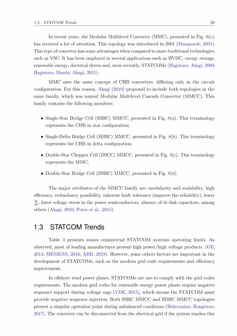
Figure 8 – MMCC family members: (a) Single-Star Bridge Cell (SSBC) MMCC;
(b) Single-Delta Bridge Cell (SDBC) MMCC; (c) Double-Star Chopper
Cell (DSCC) MMCC; (d) Double-Star Bridge Cell (DSBC) MMCC. . . 40
Figure 9 – Overview of the proposed strategies for power loss reduction in MMCC. 42
Figure 10 – (a) MMCC-based STATCOM in the electric power system; (b)
STATCOM average model; (c) Phasor diagram of STATCOM. . . . . . 44
Figure 11 – Structure of the Master Thesis. . . . . . . . . . . . . . . . . . . . . . . 45
Figure 12 – Schematic of the DSCC MMCC-based STATCOM. . . . . . . . . . . . 49
Figure 13 – Arm-average model of a DSCC MMCC-based STATCOM. . . . . . . . 50
Figure 14 – Equivalent circuit showing the behavior of the: (a) output currents; (b)
circulating currents. . . . . . . . . . . . . . . . . . . . . . . . . . . . . 51
Figure 15 – Qualitative analysis of the effective dc-link voltage design: (a) negligible
dc-link voltage ripple assuming that the converter absorbs rated reactive
power; (b) non-negligible dc-link voltage ripple assuming that the
converter absorbs rated reactive power (with overmodulation); (c)
non-negligible dc-link voltage ripple assuming that the converter absorbs
rated reactive power (without overmodulation); (d) negligible dc-link
voltage ripple assuming that the converter provides rated reactive
power; (e) non-negligible dc-link voltage ripple assuming that the
converter provides rated reactive power (without overmodulation); (f)
non-negligible dc-link voltage ripple assuming that the converter provides
rated reactive power (without overmodulation). . . . . . . . . . . . . . 56
Figure 16 – (a) STATCOM average model; (b) Phasor diagram of STATCOM. . . . 57

Figure 17 – Output voltage (rms) synthesized by the converter. . . . . . . . . . . . 57
Figure 18 – (a) Insertion index limited by the zero voltage; (b) Insertion index
limited by the sum of capacitor voltage ripples. . . . . . . . . . . . . . 59
Figure 19 – Minimum dc-link voltage for operation in the linear region of the
modulator as function of the operating angle of the output current
(parameters in Table 5). . . . . . . . . . . . . . . . . . . . . . . . . . . 62
Figure 20 – Phasor diagram of STATCOM (a) absorbing reactive power; (b)
providing reactive power. Remark: is = Is cos(ωnt − φ). . . . . . . . . . 63
Figure 21 – Minimum dc-link voltage as function of the operating angle of the output
current and the current output Is (parameters in Table 5). . . . . . . . 63
Figure 22 – Minimum dc-link voltage as function of the operating reactive power
and (a) cell capacitance variation, (b) output reactance variation. . . . 64
Figure 23 – Number of unnecessary cells as function of the operating reactive power
and (a) cell capacitance variation, (b) reactance variation. . . . . . . . 65
Figure 24 – Qualitative analysis of the DSCC MMCC-based STATCOM operation
during the insertion transient: (a) Ideal waveforms for hot standby
operation; (b) Ideal waveforms for operation in overmodulation region
for rated reactive power supply operation (before insertion); (c) Ideal
waveforms for operation for rated reactive power supply operation (after
insertion); (d) Ideal waveforms for hot standby operation; (e) Ideal
waveforms for operation in overmodulation region for rated reactive
power absorption operation (before insertion); (f) Ideal waveforms for
operation for rated reactive power absorption operation (after insertion). 71
Figure 25 – Conduction states of the bypass switch elements during the bypass and
insertion procedures. The maximum delay of the contactor is assumed
to be equal to 60 ms for both turn-on and turn-off. . . . . . . . . . . . 73
Figure 26 – Direct voltage control of a DSCC MMCC-based STATCOM. . . . . . . 76
Figure 27 – Closed-loop voltage control of a DSCC MMCC-based STATCOM. . . . 76
Figure 28 – Open-loop voltage control of a DSCC MMCC-based STATCOM. . . . . 77
Figure 29 – Complete control strategy of a DSCC MMCC-based STATCOM. . . . 78
Figure 30 – Block diagram of the modulation method. . . . . . . . . . . . . . . . . 79
Figure 31 – Block diagram of the output current control. . . . . . . . . . . . . . . . 81
Figure 32 – Block diagram of the circulating current control. . . . . . . . . . . . . . 82
Figure 33 – Block diagram of the global energy control. . . . . . . . . . . . . . . . . 83
Figure 34 – Reactive power reference profile employed in the simulation. . . . . . . 85
Figure 35 – Methodology for energy loss (MWh) calculation for an one-year mission
profile. . . . . . . . . . . . . . . . . . . . . . . . . . . . . . . . . . . . . 86
Figure 36 – Mission profile of (a) ambient temperature, (b) reactive power. . . . . . 86

Figure 37 – Data extracted from a power module datasheet (part number
FF800R17KP4-B2): (a) Turn-on switching energy (IGBT); (b) Turn-off
switching energy (IGBT); (c) Reverse recovery energy (diode); (d)
Typical IGBT on-state characteristics; (e) Typical diode forward
characteristics. . . . . . . . . . . . . . . . . . . . . . . . . . . . . . . . 87
Figure 38 – Thermal model of the power devices in a chopper cell with common
heatsink. . . . . . . . . . . . . . . . . . . . . . . . . . . . . . . . . . . . 88
Figure 39 – Dynamic behavior of the instantaneous active and reactive power when
the converter is subjected to the reference profile of Fig. 34. . . . . . . 93
Figure 40 – Dynamic behavior of the total MMCC storage energy when the converter
is subjected to the reference profile of Fig. 34. . . . . . . . . . . . . . . 94
Figure 41 – (a) Dynamic behavior of the cell capacitor voltages of phase A (upper
arm) when the converter is subjected to the reference profile of Fig. 34,
(b) detail in reactive power absorption operation, (c) detail in reactive
power supply operation. . . . . . . . . . . . . . . . . . . . . . . . . . . 94
Figure 42 – (a) Dynamic behavior of the DSCC MMCC-based STATCOM when 4
cells are bypassed: (a) cell capacitor voltages of upper arm (phase A),
(b) number of inserted cells, (c) output current. . . . . . . . . . . . . . 95
Figure 43 – (a) Dynamic behavior of the DSCC MMCC-based STATCOM when 4
cells are inserted: (a) cell capacitor voltages of upper arm (phase A),
(b) number of inserted cells, (c) output current. . . . . . . . . . . . . . 96
Figure 44 – Dynamic behavior of the circulating current when the converter is
subjected to the reference profile of Fig. 34. . . . . . . . . . . . . . . . 97
Figure 45 – (a) Dynamic behavior of the output current when the converter is
subjected to the reference profile of Fig. 34, (b) detail in reactive power
absorption operation, (c) detail in reactive power supply operation. . . 97
Figure 46 – (a) Inserted voltage and sum of capacitor voltages estimation of the
phase A (upper arm), (b) detail in reactive power absorption operation,
(c) detail in reactive power supply operation. . . . . . . . . . . . . . . . 98
Figure 47 – (a) Insertion number for the upper arm, (b) detail in reactive power
absorption operation, (c) detail in reactive power supply operation. . . 99
Figure 48 – (a) Sum of capacitor voltages (estimated and measured), (b) detail in
reactive power absorption operation, (c) detail in reactive power supply
operation. . . . . . . . . . . . . . . . . . . . . . . . . . . . . . . . . . . 100
Figure 49 – DSCC MMCC-based STATCOM losses with reactive power
compensation variation. w refers to with the methodology proposed,
i.e., the minimum cell operation control. w/o refers to not using the
methodology proposed, i.e, the conventional control. . . . . . . . . . . . 101


List of Tables
Table 1 – Comparison among technologies of reactive power compensation. Adapted
from: Neutz (2013). . . . . . . . . . . . . . . . . . . . . . . . . . . . . . 34
Table 2 – Summary of multilevel converters characteristics. . . . . . . . . . . . . . 38
Table 3 – STATCOMs system capability. . . . . . . . . . . . . . . . . . . . . . . . 40
Table 4 – Summary of the proposed strategies for efficiency improvement in MMCC. 43
Table 5 – Parameters of the DSCC MMCC-based STATCOM. . . . . . . . . . . . 62
Table 6 – Foster and case to heatsink parameters of the thermal model. . . . . . . 88
Table 7 – Cauer parameters of the thermal model. . . . . . . . . . . . . . . . . . . 88
Table 8 – Parameters of the heatsink and fluid cooling impedances. . . . . . . . . 90
Table 9 – Heatsink and fluid cooling impedances. . . . . . . . . . . . . . . . . . . 90
Table 10 – Parameters of the DSCC MMCC-based STATCOM. . . . . . . . . . . . 91
Table 11 – Controller parameters of the DSCC MMCC-based STATCOM. . . . . . 91
Table 12 – Benchmarking of the proposed and conventional control strategy of a
DSCC MMCC-based STATCOM. . . . . . . . . . . . . . . . . . . . . . 98
Table 13 – DSCC MMCC-based STATCOM energy consumption (EC) for an
one-year mission profile. . . . . . . . . . . . . . . . . . . . . . . . . . . . 100


List of abbreviations and acronyms
ABB Asea Brown Boveri (Swedish-Swiss multinational corporation)
ac Alternating Current
BPF Band-Pass Filtering
CAPEX Capital Expenditure
CHB Cascaded H-bridge
dc Direct Current
DSBC Double-Star Bridge Cell
DSCC Double-Star Chopper Cell
DPWM Discontinuous Pulse Width Modulation
EC Energy Consumption
FC Flying Capacitor
FPGA Field Programmable Gate Array
GE General Electric
GTO Gate Turn-Off Thyristor
HVDC High-Voltage Direct Current
IGBT Insulated Gate Bipolar Transistor
IGCT Integrated Gate-Comutated Thyristor
LMMC Lattice Modular Multilevel Converter
LPF Low Pass Filter
MAF Moving Average Filter
MMC Modular Multilevel Converter
MMCC Modular Multilevel Cascade Converter
MTTR Mean Time To Repair

NLC Nearest Level Control
NPC Neutral Point Clamped
OPEX Operational Expenditure
PCB Printed Circuit Board
PCC Point of Common Coupling
PI Proportional Integral
PIM Plastic IGBT Modules
PR Proportional Resonant
pu Per Unit
PWM Pulse Width Modulation
rms Root Mean Square
SC Synchronous Condensers
SDBC Single-Delta Bridge Cell
SHE PWM Selective Harmonic Elimination Pulse Width Modulation
SSBC Single-Star Bridge Cell
SSSC Static Synchronous Series Compensator
STATCOM Static Synchronous Compensator
SVC Static VAR Compensator
TCSC Thyristor-Controlled Series Capacitor
TDD Total Demand Distortion
VSC Voltage Source Converter
zoh Zero-order Hold

List of symbols
Ah Heatsink surface area
C Cell capacitance
ch Specific heat capacity
Ch−a Heatsink-to-ambient thermal capacitance
Ch−f Heatsink-to-fluid thermal capacitance
D1 Bottom diode of the chopper cell
D2 Top diode of the chopper cell
dh Heatsink thickness
fc Fluid flow convection coefficient
fm Frequency of the capacitor voltage ripple
fn Line frequency
fsw Sampling frequency
il Lower arm current
Is Output current amplitude
is Output current
isαβ Output current in stationary reference frame
iu Upper arm current
Imax Maximum amplitude of arm current
Ips Rated current of the semiconductor device
ix,avg Average current values in the switch x (S1, S2, D1 or D2)
ix,rms rms current values in the switch x (S1, S2, D1 or D2)
iz Circulating current
izac Fundamental component of the circulating current

izdc dc component of the circulating current
kh Thermal conductivity of the heatsink material
KI Current sizing factor
ki,W Integral gain of the energy controller
kp,I Proportional gain of the output current controller
kp,W Proportional gain of the energy controller
kp,Z Proportional gain of the circulating current controller
kr,I Resonant gain of the output current controller
kr,Z Resonant gain of the circulating current controller
Larm Arm inductance
Lf Transformer inductance
mmax Maximum modulation index
mi Modulation index
mu Ideal modulation signal of upper arm
N Number of cells
Nf Number of unnecessary cells
nl Lower arm insertion index
Nmin Minimum number of cells
nu Upper arm insertion index
P Active power
p3n Three-phase instantaneous active power
Pcond,x Conduction losses of the switch x (S1, S2, D1 or D2)
Pind Ohmic losses in the inductor
pl Lower arm instantaneous active power
pu Upper arm instantaneous active power
Rarm Arm resistance

Rf Transformer resistance
Rf−a Fluid-to-ambient thermal resistance
Rh−a Heatsink-to-ambient thermal resistance
Rh−f Heatsink-to-fluid thermal resistance
rx Resistance of the switch x (S1, S2, D1 or D2)
S1 Bottom IGBT of the chopper cell
S2 Top IGBT of the chopper cell
Sn Rated power
ST Vacuum contactor of the bypass structure
T Thyristor of the bypass structure
t Time
Ta Ambient temperature
Tc Case temperature
Tj Junction temperature
Tsw Sampling time
vcell Nominal cell voltage
vd dc-link voltage
vd0 Minimum dc-link voltage limited by the zero voltage
vd,min Minimum dc-link voltage for operation in the linear region
vdn Nominal dc-link voltage
Vg Amplitude grid voltage
Vg rms grid voltage
vg Grid voltage
vgαβ Grid voltage in stationary reference frame
vl Lower arm voltage
Vs Output voltage amplitude
vs Output voltage
vu Upper arm voltage
Vx Voltage of the switch x (S1, S2, D1 or D2)
vz Internal voltage
vΣCl Sum of the capacitor voltages of the lower arm
vΣCu Sum of the capacitor voltages of the upper arm
Q Reactive power
xeq Equivalent output reactance
xeq(pu) Maximum per unit value of the output reactance
WT Total MMCC storage energy
Zc−h Case-to-heatsink thermal impedance
Zj−c Junction-to-case thermal impedance
Zh−a Heatsink-to-ambient thermal impedance
∆V Voltage ripple
∆vd dc-link voltage ripple
∆Vg Grid voltage variation
∆xeq Output reactance variation
∆W∆ Difference of the upper and lower arm energies
∆WΣ Sum of the upper and lower arm energies
φ Displacement angle of the output current
ωn Line frequency in rad/s
θz Angle that define the arm current zero-crossings
Λmax Maximum modulation gain
ρh Heatsink material density
Superscripts
∗ Reference value

Subscripts
, a Phase A
, b Phase B
, c Phase C
, abs STATCOM absorbs reactive power
, prov STATCOM provides reactive power
, n Phases A, B or C
, x Switch of the chopper cell (S1, S2, D1 or D2)

Contents
1 INTRODUCTION . . . . . . . . . . . . . . . . . . . . . . . . . . . . . 31
1.1 Context and Relevance . . . . . . . . . . . . . . . . . . . . . . . . . . 31
1.2 STATCOM Realization . . . . . . . . . . . . . . . . . . . . . . . . . . . 34
1.3 STATCOM Trends . . . . . . . . . . . . . . . . . . . . . . . . . . . . . 39
1.4 Overview of the Proposed Strategies for Efficiency Improvement
in MMCC . . . . . . . . . . . . . . . . . . . . . . . . . . . . . . . . . . 41
1.5 Purpose and Contributions . . . . . . . . . . . . . . . . . . . . . . . 44
1.6 Master Thesis Outline . . . . . . . . . . . . . . . . . . . . . . . . . . . 45
1.7 List of Publications . . . . . . . . . . . . . . . . . . . . . . . . . . . . 46
2 DSCC MMCC-BASED STATCOM . . . . . . . . . . . . . . . . . . . . 49
2.1 Topology . . . . . . . . . . . . . . . . . . . . . . . . . . . . . . . . . . 49
2.2 Dynamic Modelling . . . . . . . . . . . . . . . . . . . . . . . . . . . . 50
2.2.1 Instantaneous power flow in DSCC MMCC . . . . . . . . . . . . . . . . 52
2.3 Insertion Indexes . . . . . . . . . . . . . . . . . . . . . . . . . . . . . 54
2.4 Dc-link Voltage Design . . . . . . . . . . . . . . . . . . . . . . . . . . 55
2.5 Chapter Conclusions . . . . . . . . . . . . . . . . . . . . . . . . . . . 57
3 MINIMUM CELL OPERATION CONTROL . . . . . . . . . . . . . . . 59
3.1 Limits of Linear Modulation Region: Minimum dc-link Voltage . . 59
3.2 Analysis of the Minimum Cell Operation Control . . . . . . . . . . . 63
3.2.1 Potential of Bypassing Unnecessary Cells . . . . . . . . . . . . . . . . 63
3.2.2 Potential to Reduce Conduction Losses . . . . . . . . . . . . . . . . . 64
3.3 Limitations . . . . . . . . . . . . . . . . . . . . . . . . . . . . . . . . . 68
3.3.1 Minimum number of cells Nmin . . . . . . . . . . . . . . . . . . . . . . . 68
3.3.2 Maximum number of bypassed cells Nf,prov and Nf,abs . . . . . . . . . 70
3.4 Bypass and Insertion Procedures . . . . . . . . . . . . . . . . . . . 72
3.5 Chapter Conclusions . . . . . . . . . . . . . . . . . . . . . . . . . . . 73
4 CONTROL STRATEGY AND CONTROL TUNING . . . . . . . . . . 75
4.1 Control Strategies . . . . . . . . . . . . . . . . . . . . . . . . . . . . . 75
4.1.1 Direct voltage control . . . . . . . . . . . . . . . . . . . . . . . . . . . . 75
4.1.2 Closed-loop voltage control . . . . . . . . . . . . . . . . . . . . . . . . 76
4.1.3 Open-loop voltage control . . . . . . . . . . . . . . . . . . . . . . . . . 77
4.2 Control Tuning . . . . . . . . . . . . . . . . . . . . . . . . . . . . . . . 80
4.2.1 Output current control . . . . . . . . . . . . . . . . . . . . . . . . . . . 80

4.2.2 Circulating current control . . . . . . . . . . . . . . . . . . . . . . . . . 81
4.2.3 Global energy control . . . . . . . . . . . . . . . . . . . . . . . . . . . . 82
4.3 Chapter Conclusions . . . . . . . . . . . . . . . . . . . . . . . . . . . 84
5 CASE STUDY AND SYSTEM PARAMETERS . . . . . . . . . . . . . 85
5.1 Case Study . . . . . . . . . . . . . . . . . . . . . . . . . . . . . . . . . 85
5.1.1 Dynamic Behavior . . . . . . . . . . . . . . . . . . . . . . . . . . . . . . 85
5.1.2 Energy Consumption . . . . . . . . . . . . . . . . . . . . . . . . . . . . 85
5.2 System Parameters . . . . . . . . . . . . . . . . . . . . . . . . . . . . 90
5.3 Chapter Conclusions . . . . . . . . . . . . . . . . . . . . . . . . . . . 91
6 RESULTS . . . . . . . . . . . . . . . . . . . . . . . . . . . . . . . . . 93
6.1 Dynamic Behavior . . . . . . . . . . . . . . . . . . . . . . . . . . . . . 93
6.2 Energy Consumption . . . . . . . . . . . . . . . . . . . . . . . . . . . 99
6.3 Chapter Conclusions . . . . . . . . . . . . . . . . . . . . . . . . . . . 100
7 CLOSURE . . . . . . . . . . . . . . . . . . . . . . . . . . . . . . . . . 103
7.1 Conclusions . . . . . . . . . . . . . . . . . . . . . . . . . . . . . . . . 103
7.2 Future Works . . . . . . . . . . . . . . . . . . . . . . . . . . . . . . . . 104
REFERENCES . . . . . . . . . . . . . . . . . . . . . . . . . . . . . . 105
APPENDIX 113
APPENDIX A – MATHEMATICAL DEVELOPMENTS - CHAPTER 3 115
A.1 Derivation of (3.11) . . . . . . . . . . . . . . . . . . . . . . . . . . . . . 115
APPENDIX B – IGBT MODULE . . . . . . . . . . . . . . . . . . . . 117
B.1 Arm currents . . . . . . . . . . . . . . . . . . . . . . . . . . . . . . . . 117
B.2 Current efforts in semiconductor devices . . . . . . . . . . . . . . . 117
B.3 Voltage rating . . . . . . . . . . . . . . . . . . . . . . . . . . . . . . . 118
31
1 Introduction
1.1 Context and Relevance
The current power systems scenario is characterized by complex and time-variant
structures, presence of nonlinear loads (such as electric drives, electric arc furnaces, etc) and
high penetration of renewable energy such as solar and wind power plants (Dhal; Rajan,
2014; Ma; Huang; Zhou, 2015). These phenomena can lead to grid voltage disturbances,
reactive current and power quality deterioration, which affects the power system overall
efficiency (Dixon et al., 2005).
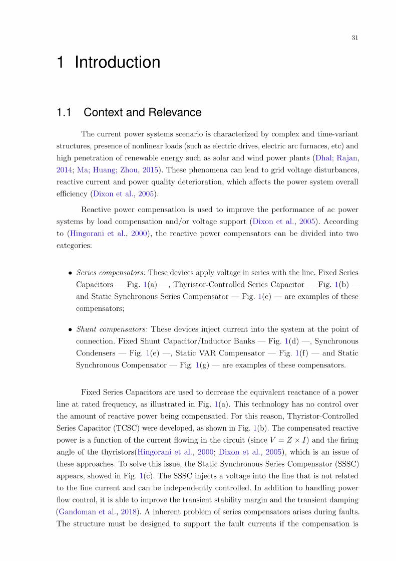
Reactive power compensation is used to improve the performance of ac power
systems by load compensation and/or voltage support (Dixon et al., 2005). According
to (Hingorani et al., 2000), the reactive power compensators can be divided into two
categories:
• Series compensators : These devices apply voltage in series with the line. Fixed Series
Capacitors — Fig. 1(a) —, Thyristor-Controlled Series Capacitor — Fig. 1(b) —
and Static Synchronous Series Compensator — Fig. 1(c) — are examples of these
compensators;
• Shunt compensators: These devices inject current into the system at the point of
connection. Fixed Shunt Capacitor/Inductor Banks — Fig. 1(d) —, Synchronous
Condensers — Fig. 1(e) —, Static VAR Compensator — Fig. 1(f) — and Static
Synchronous Compensator — Fig. 1(g) — are examples of these compensators.
Fixed Series Capacitors are used to decrease the equivalent reactance of a power
line at rated frequency, as illustrated in Fig. 1(a). This technology has no control over
the amount of reactive power being compensated. For this reason, Thyristor-Controlled
Series Capacitor (TCSC) were developed, as shown in Fig. 1(b). The compensated reactive
power is a function of the current flowing in the circuit (since V = Z × I) and the firing
angle of the thyristors(Hingorani et al., 2000; Dixon et al., 2005), which is an issue of
these approaches. To solve this issue, the Static Synchronous Series Compensator (SSSC)
appears, showed in Fig. 1(c). The SSSC injects a voltage into the line that is not related
to the line current and can be independently controlled. In addition to handling power
flow control, it is able to improve the transient stability margin and the transient damping
(Gandoman et al., 2018). A inherent problem of series compensators arises during faults.
The structure must be designed to support the fault currents if the compensation is

32 Chapter 1. Introduction
required in such events. Otherwise, a bypass structure must be employed (Hingorani et al.,
2000; Silva, 2003; Dixon et al., 2005).
Load
(a)
Source
Load
Source
Load
Source
Load
Source
Load
Source
Load
Source
Load
Source
( )d
( )f
( )c
( )g
( )b
( )e
Figure 1 – Reactive power compensators: (a) Fixed Series Capacitors; (b)Thyristor-Controlled Series Capacitor (TCSC); (c) Static SynchronousSeries Compensator (SSSC); (d) Fixed Shunt Capacitor/Inductor Bank ; (e)Synchronous Condensers (SC); (f) Static VAR Compensator (SVC); (g) StaticSynchronous Compensator (STATCOM).
Regarding the shunt compensation, Fixed Shunt Capacitor/Inductor Bank — Fig.
1(b) — was used to correct power factor in 1914. Despite their simplicity and lower cost,

1.1. Context and Relevance 33
these solutions cannot change the compensation amount of the reactive power, which is not
efficient when the reactive power varies over a wide range. From the late 1920s until the
late 1970s, several Synchronous Condensers (SC), as shown Fig. 1(e), were used in electrical
power systems. However, synchronous condensers require considerable foundations and a
significant amount of starting and protection devices. In addition, they represent a part
in short-circuit current, and they cannot be adjusted fast enough to balance fast load
changes. Furthermore, their losses and costs are much higher than those observed in static
compensators. Nevertheless, they are still widely used, due to the additional capacity to
provide inertia, which is very important in primary frequency regulation (Hingorani et al.,
2000; Dixon et al., 2005; Singh et al., 2009; Igbinovia et al., 2015).
In the 1970s, the technology of thyristor valves and digital controls were initially
extended to the development of Static VAR Compensator (SVC) for load compensation
and voltage regulation in long transmission lines, as illustrated in Fig. 1(f). It addresses
the problem of keeping steady-state and dynamic voltages within bounds (Hingorani et al.,
2000; Dixon et al., 2005; Singh et al., 2009; Igbinovia et al., 2015). Furthermore, SVCs are
used to improve the dynamic stability, damp power swings and reduce system losses by
using reactive power control. However, the ability to compensate reactive power depends
on the voltage (Q = V 2
X), i.e., the compensation margin decreases during voltage sags
(Gandoman et al., 2018).
The Static Synchronous Compensator (STATCOM) has become a prominent device
for reactive power compensation and dynamic performance improvement in the power
systems (Shinde; Pulavarthi, 2017). It was developed as an advance of the SVC and is
based on Voltage Source Converter (VSC) using IGBTs, IGCTs or GTOs, as shown in Fig.
1(g). The major attributes of STATCOM are (Padiyar, 2007; Singh et al., 2009; Gandoman
et al., 2018):
• Fast time response;
• Smaller footprint;
• Lower harmonic distortion;
• Better support during voltage disturbances;
• Independence of the voltage applied;
• Higher operational flexibility;
• Excellent dynamic characteristics under various operating conditions.
Neutz (2013) presents a comparison of some reactive power shunt compensators, as
shown in Table 1. As observed, STATCOM is an interesting candidate for reactive power

34 Chapter 1. Introduction
compensation during fast transients. A feature of this device is that it is hot stand-by.
This results in an increase in the operational expenditure.
Table 1 – Comparison among technologies of reactive power compensation. Adapted from:Neutz (2013).
TechnologySpeed ofResponse
RepeatedOperationPossible
StepsInertia
(active power)Cost CAPEX1
/OPEX2
Fixed ShuntCapacitor/Inductor
BankSlow
Dischargetime and wearof switchgear
Fixed No Low
SVC Fast Continuous Continuous NoCheaper thanSTATCOM forlarge systems
SC Fast Continuous Continuous YesHigh OPEX,bad MTTR3,
permanent losses
STATCOM Fast Continuous ContinuousPossible withadded energy
storage
High CAPEXif no hybridsolution
1CAPEX is the capital expenditure and it is related to converter cost: capacitors, magnetic devices,semiconductor devices, controllers, PCBs, cooling system, among others.
2OPEX is the operational expenditure and it is mainly associated to the maintenance costs and the costs of thepower losses.
3The Mean Time To Repair (MTTR) is the time needed to repair a failed hardware module.
Static Synchronous Compensators have been employed at different power and
voltage levels. At the distribution voltage level, STATCOMs are mainly used to
mitigate power quality problems (Reed; Takeda; Iyoda, 1999). At the transmission and
sub-transmission voltage levels, STATCOMs have been employed for voltage control
and power oscillation damping (Hingorani et al., 2000; Zhang et al., 2006). In large
renewable energy power plants, STATCOMs have been employed for fast reactive power
compensation and grid code fulfillment (Neutz, 2013). In recent years, energy storage
systems have been integrated in STATCOMs to provide inertia and frequency regulation
capabilities (Chakraborty et al., 2012). Modernization of the power system in terms of
reactive power compensation is expected as it tends to replace traditional thyristor systems
with STATCOM systems, similarly to what happened in High-Voltage Direct Current
(HVDC) systems (Behrouzian, 2016).
1.2 STATCOM Realization
The early STATCOMs were based on two-level converters. Since the number of
voltage levels is quite reduced, high switching frequencies must be employed to comply with
the harmonic standards. Moreover, the converter output voltage is limited in the kilovolts
range because of the limited blocking voltage of the commercial available semiconductor
devices (up to 6.5 kV for silicon-based devices). Therefore, a step-up transformer is required,
as illustrated in Fig. 2. This transformer reduces the converter efficiency and increases the
STATCOM weight and volume (Sharifabadi et al., 2016).

1.2. STATCOM Realization 35
S2
S1
D2
D1
C
C
vd
1
2
Figure 2 – Two-level voltage source converter.
On the other hand, it is possible to connect several semiconductor devices in series
to increase the output voltage and remove the step-up transformer. However, it is still
necessary to guarantee the operation and fault tolerance of these semiconductor switches
(Sharifabadi et al., 2016). This topology is illustrated in Fig. 3(a). Another solution is the
use of multi-stage transformer topologies shown in Fig. 3(b). Nevertheless, the use of this
type of transformer makes the project very expensive, very large and inefficient (Fujii;
Schwarzer; De Doncker, 2005).
Sn+1
S1
Dn+1
D1
C
C
vd
Sn D
n
S2n D
2n
1
2
S2
S1
D2
D1C
vd
S4
S3
D4
D3 Y Y
Y Y
ditto
(a)
(b)
Figure 3 – Two-level voltage source converter with: (a) series connection of semiconductorswitches; (b) multi-stage transformer.
In addition, when the power is high, the two-level converters are connected
in parallel and multi-pulse converters appear. The 12-pulse converters require twice
two-level converters (Fig 4(a)) connected in parallel over the single dc-link where they are
series-connected to transformers on the output side as seen in Fig 4(b). This approach
requires a different transformer connection for each two-level VSC. The main improvement
of the multi-pulse converters is the cancellation of the harmonics in sidebands at the entire
multiple frequencies of the number of pulses of the converter (Shahnia; Rajakaruna; Ghosh,
2014).
Furthermore, a quasi 24-pulse converter requires four two-level VSC connected

36 Chapter 1. Introduction
in parallel, as shown in Fig 4(c) (Shahnia; Rajakaruna; Ghosh, 2014). A problem with
this approach is the transformer, which increases the volume and the energy losses of the
STATCOM.
S2
S1
D2
D1
C
Cvd
1
2
Y
Y
(a)
(b)
C
Cvd
1
2
Y
Y
Y
(c)
Figure 4 – (a) Two-level voltage source converter; (b) 12-pulse converter; (c) quasi 24-pulseconverter.
An alternative to overcome the limitations of two-level VSC is the multilevel
converter concept. The multilevel topologies show improvements in harmonic properties
and do not require direct series connection for increasing the operating voltage. The most
common multilevel converter topologies are the Neutral Point Clamped (NPC), Flying
Capacitor converter (FC), Cascaded H-bridge converter (CHB) and Modular Multilevel
Converter (MMC) (Franquelo et al., 2008).
NPC (Fig. 5) was the first multilevel topology used on a large scale, introduced
in 1979 (Baker, 1979). However, the application of medium voltage is limited by the
number of levels due to the complexity of the system and large number of components
required (Sharifabadi et al., 2016). Another disadvantage is the uneven distribution of
losses between the semiconductors, which limits the switching frequency and the output
power (Behrouzian; Bongiorno; De La Parra, 2013). As in the two-level converter, NPC
converters can be connected in parallel for 12-pulse and 24-pulse converters, as shown in
Figs. 6(b) and 6(c), respectively (Shahnia; Rajakaruna; Ghosh, 2014).
The Flying Capacitor (FC) converter was introduced by Meynard and Foch (1992)

1.2. STATCOM Realization 37
S1 D
1
C
C
vd
S2 D
2
1
2
S3 D
3
S4 D
4
D5
D6
Figure 5 – Neutral Point Clamped (NPC) converter.
C
Cvd
1
2
Y
S1 D
1
S2 D
2
S3 D
3
S4 D
4
D5
D6
(a)
(b)
C
Cvd
1
2
Y
Y
+7.5°
+7.5°
-7.5°
-7.5°
(c)
Figure 6 – (a) NPC converter; (b) 12-pulse converter; (c) 24-pulse converter.
and can be considered as an alternative to overcome some of the NPC drawbacks. This
topology is shown in Fig. 7. Additional output levels are achieved through capacitors.
It provides redundant switching states that can be used to control the capacitor charge.
Moreover, this converter can achieve loss equalization, natural capacitor balancing and
superior harmonic performance. However, when the number of levels increase, the circuit
becomes very complex due to the increase in the number of flying capacitors connected at
different points by semiconductor devices that create many meshes. This complicates the
mechanical design of the converter (Behrouzian; Bongiorno; De La Parra, 2013; Sharifabadi
et al., 2016).
Cascaded connection of bridge cells was introduced in the 1970s for single-phase

38 Chapter 1. Introduction
S1 D1C
C
vd
S2 D2
1
2
S3 D3
S4 D4
Cf
Figure 7 – Flying Capacitor (FC) converter.
system (Mcmurray, 1971; Baker; Bannister, 1975). A three-phase STATCOM based on
star-connected cascaded multilevel converter (Fig. 8(a)) was proposed in 1996 by Fang
Zheng Peng et al. (1996). In addition, a three-phase STATCOM based on delta-connected
cascaded multilevel converter, Fig. 8(b), was proposed in 2004 by Peng and Jin Wang
(2004). In this topology, no clamping components are necessary and low switching frequency
can be used (Fujii; Schwarzer; De Doncker, 2005). CHB consists of many full bridge cells
connected in series. This structure can reach medium output voltage levels using low-voltage
and mature semiconductors technology. In addition, the topology is modular, which leads
to a fault-tolerant structure (Behrouzian; Bongiorno; De La Parra, 2013).
Franquelo et al. (2008), Behrouzian, Bongiorno and De La Parra (2013) present a
comparison of some characteristics of NPC, FC and CHB multilevel converters, as shown
in Table 2. As observed, the CHB presents good characteristics justifying its use in several
applications. This converter was first adopted by Alstom for high-powered STATCOMs
employing GTOs (Ainsworth et al., 1998). Furthermore, manufacturers like ABB, Siemens
and GE already market the STATCOMs based on this converter topology (GE, 2016;
ABB, 2019; SIEMENS, 2019b).
Table 2 – Summary of multilevel converters characteristics.
Characteristics NPC FC CHB
Modularity Low High HighFault tolerance Difficult Easy Easy
Reliability Low Low HighLoss distribution Unequal Uniform Uniform
Low switching CapableCapable with large
capacitorsCapable with higher
voltage levelsMaximum practical
levels3-5 levels 5-7 levels No theoretical limit
Common dc-link Yes Yes NoEfficiency Medium Medium High
1.3. STATCOM Trends 39
In recent years, the Modular Multilevel Converter (MMC), presented in Fig. 8(c),
has received a lot of attention. This topology was introduced in 2001 (Marquardt, 2001).
This type of converter has some advantages when compared to more traditional technologies,
such as VSC. It has been employed in several applications such as HVDC, energy storage,
renewable energy, electrical drives and, more recently, STATCOMs (Hagiwara; Akagi, 2009;
Hagiwara; Maeda; Akagi, 2011).
MMC uses the same concept of CHB converters, differing only in the circuit
configuration. For this reason, Akagi (2010) proposed to include both topologies in the
same family, which was named Modular Multilevel Cascade Converter (MMCC). This
family contains the following members:
• Single-Star Bridge Cell (SSBC) MMCC, presented in Fig. 8(a). This terminology
represents the CHB in star configuration;
• Single-Delta Bridge Cell (SDBC) MMCC, presented in Fig. 8(b). This terminology
represents the CHB in delta configuration;
• Double-Star Chopper Cell (DSCC) MMCC, presented in Fig. 8(c). This terminology
represents the MMC;
• Double-Star Bridge Cell (DSBC) MMCC, presented in Fig. 8(d).
The major attributes of the MMCC family are: modularity and scalability, high
efficiency, redundancy possibility, inherent fault tolerance (improve the reliability), lowerdvdt, lower voltage stress in the power semiconductors, absence of dc-link capacitors, among
others (Akagi, 2010; Perez et al., 2015).
1.3 STATCOM Trends
Table 3 presents somes commercial STATCOM systems operating limits. As
observed, most of leading manufactures present high power/high voltage products. (GE,
2014; SIEMENS, 2016; ABB, 2019). However, some others factors are important in the
development of STATCOMs, such as the modern grid code requirements and efficiency
improvement.
In offshore wind power plants, STATCOMs are use to comply with the grid codes
requirements. The modern grid codes for renewable energy power plants require negative
sequence support during voltage sags (VDE, 2015), which means the STATCOM must
provide negative sequence injection. Both SSBC MMCC and SDBC MMCC topologies
present a singular operation point during unbalanced conditions (Behrouzian; Bongiorno,
2017). The converter can be disconnected from the electrical grid if the system reaches this

40 Chapter 1. Introduction
CS1
S2
D1
D2
Cell N
Cell 2 Clu
ster
BCS3
S4
D3
D4
Clu
ster
CA
Lcl
ABC
LfLfLf
LclLcl
CS1
S2
D1
D2
Cell N
Cell 2 Clu
ster
BCS3
S4
D3
D4
Clu
ster
CA
Lcl
ABC
LfLfLf
LclLcl
CS1
S2
D1
D2
Cell N
Cell 2
S3
S4
D3
D4
Larm
Larm
Low
er a
rmA
Larm
Larm
Low
er a
rm B
Larm
Larm
Low
er a
rm C
Upper
arm
B
Upper
arm
C
Lf
ABC
CS1
S2
D1
D2
Cell N
Cell 2
Larm
Larm
Low
er a
rmA
Larm
Larm
Low
er a
rm B
Larm
Larm
Low
er a
rm C
Upper
arm
B
Upper
arm
C
Lf
ABC
(a) (b)
(c) (d)
Figure 8 – MMCC family members: (a) Single-Star Bridge Cell (SSBC) MMCC; (b)Single-Delta Bridge Cell (SDBC) MMCC; (c) Double-Star Chopper Cell (DSCC)MMCC; (d) Double-Star Bridge Cell (DSBC) MMCC.
Table 3 – STATCOMs system capability.
Trade Mark ManufacturerReactive PowerOperating Range
Voltage OperatingRange
SVC Light ABBup to 360 Mvar
(inductive and capacitive)up to 69 kV
GE-STATCOM GEup to 300 Mvar
(inductive and capacitive)up to 63 kV
SVC Plus Siemensup to 70 Mvar (inductive)and 100 Mvar (capacitive)
up to 132 kV

1.4. Overview of the Proposed Strategies for Efficiency Improvement in MMCC 41
singular point. In this scenario, recent publications indicate DSCC MMCC as the most
suitable for STATCOMs which are submitted to unbalanced voltage conditions (Cupertino
et al., 2019a; Tanaka et al., 2019).
On the other hand, STATCOMs are usually hot stand-by devices and its operational
costs are very relevant. The overall cost of the STATCOM is given by CAPEX +
OPEX (Tsolaridis et al., 2016). CAPEX is the capital expenditure and OPEX is the
operational expenditure. CAPEX is related to converter cost: capacitors, magnetic devices,
semiconductor devices, controllers, PCBs, cooling system, among others. OPEX is mainly
associated to the maintenance costs and the costs of the power losses (Cupertino, 2019).
Due to the important role of the power losses in the STATCOM cost, some studies
have proposed techniques to reduce power losses in MMCC. The present Master Thesis
aims to improve the efficiency of a MMCC-based STATCOM. Next section presents an
overview of the strategies proposed in literature for efficiency improvement in MMCC.
1.4 Overview of the Proposed Strategies for Efficiency
Improvement in MMCC
This Master Thesis classifies the strategies for efficiency improvement into four
groups, as shown in Fig. 9: Cell design, circulating current control, modulation schemes
and control strategies.
Regarding cell design, Modeer, Nee and Norrga (2011), Solas et al. (2013), Sousa et
al. (2018) compared different cell topologies in terms of power losses for HVDC application.
The idea is to use cell topologies that have lower power losses in semiconductor devices.
Lin et al. (2016) propose the hybrid MMCC as a fault-tolerant dc solution with minimal
power losses. Each arm of the converter is composed of a series connection of full-bridge
and half-bridge cells. Furthermore, Oliveira and Yazdani (2017) propose a topology (lattice
modular multilevel converter — LMMC —) more efficient than the half-bridge, full-bridge
and clamp-double cells, while it offers the same fault handling capability as that presented
in full-bridge cells. The use of wide band-gap devices is discussed in (Peftitsis et al.,
2012; Wu et al., 2015; Avila et al., 2017). These references indicate a significant efficiency
improvement when high switching frequencies (range of kHz) are employed. Judge et al.
(2019) proposed a bypass branch formed of series thyristors or diodes, aiming to reduce
the power losses resulting from achieving dc-fault tolerance in MMCC-HVDC systems.
Circulating current also plays an important role in MMCC losses. Jacobson et
al. (2010) propose a passive suppression method which attenuates the second harmonic
circulating current. Besides, several references employed active methods for circulating
current suppression (Tu; Xu; Xu, 2011; Li et al., 2015; Li et al., 2018). Li et al. (2018)

42 Chapter 1. Introduction
Strategies for efficiency improvement
TopologiesWide
bandgapPassive
filterActivecontrol
2nd harmonicinjection
NLC SHE PWMCell voltage
reduction
Cell design Circulatingcurrent
Modulationstrategies
Thyristorbypass
DPWMTemperature
balanceMinimum cell
operation
Control
Modeer et al.
2011
Solas et al.
2013
Sousa et al.
2018
Peftitsis et al.
2012
Wu et al.
2015
Avila et al.
2017
Judge et al.
2019Jacobson et al.
2010
Li et al.
2018
Tu et al.
2011
Li et al.
2015
Li et al.
2018
Yang et al.
2018Hassanpoor et al.
2015
Hassanpoor et al.
2016
Moranchel et al.
2015
Pérez-Basante et al.
2018
Picas et al.
2015
Farias et al.
2018
Sangwongwanich et al.
2016
ThisMaster Thesis
Lin et al.
2016
Oliveira et al.
2017
Figure 9 – Overview of the proposed strategies for power loss reduction in MMCC.
indicate passive and active methods to reduce current stress and power losses in MMCC.
Recently, Yang et al. (2018) proposed the injection of optimal second-order harmonic into
the arm current to reduce the MMCC losses. This strategy takes advantage of the superior
conduction characteristics of the anti-parallel diodes within each IGBT module to increase
the efficiency.
Different modulation strategies have been proposed to improve MMCC efficiency,
mainly focusing on switching loss reduction. Hassanpoor, Norrga and Nami (2015) studied
nearest level control (NLC) with different sorting and selection methods and compared
it with phase-shifted PWM strategy. Hassanpoor et al. (2016) proposed an optimized
sorting algorithm which concentrates the switching events at low currents and reduces
the converter switching losses. On the other hand, Moranchel et al. (2016), Perez-Basante
et al. (2018) proposed the selective harmonic elimination pulse width modulation (SHE
PWM). SHE PWM allows controlling the harmonics generated at the converter output
while it provides reduced switching losses. Picas et al. (2015) proposed the discontinuous
modulation (DPWM) to reduce the MMCC switching losses.
Farias et al. (2018) presented a control strategy for an MMCC with redundant cells.
The proposed algorithm shares the dc-link voltage among all converter cells (redundant
and non redundant) reducing the individual cell voltage and the switching losses. A
temperature balancing algorithm for MMCC is proposed by Sangwongwanich et al. (2016).
This approach can reduce the total conduction and switching losses in MMCC-HVDC
systems.
Table 4 presents a summary of the main strategies for power loss reduction in
MMCC. As observed, most of the strategies proposed in the literature require modification
in the hardware to reduce power losses. Strategies that do not require modification are
interesting for systems already installed and have a lower cost. However, most proposals

1.4. Overview of the Proposed Strategies for Efficiency Improvement in MMCC 43
that do not require modification to the hardware have the potential only to reduce switching
losses. Nevertheless, since MMCC usually employs switching frequencies in the range of
100 - 200 Hz (Eremia; Liu; Edris, 2016), the conduction losses dominate. Indeed, few
strategies to reduce conduction losses have been proposed in the literature. This Master
Thesis aims to fill this void. The goal is to use the own cell bypass structures to reduce
the power losses based on the minimum cell control operation principle.
Table 4 – Summary of the proposed strategies for efficiency improvement in MMCC.
ReferencePotential of PowerLoss Reduction
ComplexityRequiredHardware
Modification
Modeer, Nee and Norrga (2011)Solas et al. (2013)
Reduces conductionand
switching losses
High, dependingon the type ofcell adopted
Yes
Sousa et al. (2018)Reduces conduction
andswitching losses
Low Yes
Lin et al. (2016)Reduces conduction
andswitching losses
Medium Yes
Oliveira and Yazdani (2017)Reduces conduction
andswitching losses
High Yes
Peftitsis et al. (2012)Wu et al. (2015)Avila et al. (2017)
Reduces conductionand
switching lossesLow Yes
Judge et al. (2019)Reduces conduction
andswitching losses
High Yes
Jacobson et al. (2010)Reduces switching
lossesMedium Yes
Tu, Xu and Xu (2011)Li et al. (2015)Li et al. (2018)
Yang et al. (2018)
Reduces switchinglosses
Low No
Hassanpoor, Norrga and Nami (2015)Hassanpoor et al. (2016)Moranchel et al. (2016)
Perez-Basante et al. (2018)Picas et al. (2015)
Reduces switchinglosses
Medium No
Farias et al. (2018)Reduces switching
lossesMedium Yes
Sangwongwanich et al. (2016)Reduces conduction
andswitching losses
Medium No

44 Chapter 1. Introduction
1.5 Purpose and Contributions
In order to understand the proposal of this Master Thesis, let us consider the
MMCC-based STATCOM connected to the grid, as shown in Fig. 10(a). Since the MMCC
is a voltage source converter, its average steady-state behavior can be modeled by the
simplified circuit shown in Fig. 10(b).
IS
Φ Vg r Ieq S
j xeq SIVs
A
B
C
Ncells
(N - M )1
cells
(N - M )2
cells
VsVg
reqj xeq
Transmission andDistribution System
PCC
MM C STATCOMC
Generation System
Lg
SubstationIgIs
(a)
(b)
Is
Wind Farms
Photovoltaic Panels
( )c
.. .
.
.
..
.
Figure 10 – (a) MMCC-based STATCOM in the electric power system; (b) STATCOMaverage model; (c) Phasor diagram of STATCOM.
The phasor representation of Fig. 10(b) is illustrated in Fig. 10(c). As observed,
depending on the operating angle of the output current, the converter must synthesize a
voltage higher or lower than the point of common coupling (PCC) voltage. For example,
point C requires less voltage than points A and B. The voltage variation is directly related
with the magnitude of the arm inductance and the transformer impedance.
The phasor diagram suggests that, for each angle of the output current, a number
of cells is necessary to synthesize the required output voltage. The minimum cell operation
control consists in bypassing unnecessary cells from the MMCC, which reduces the number
of conducting devices. This approach can reduce conduction losses to a certain extent.
As will be shown in the next chapters, the non-negligible ripple in the MMCC capacitor
voltages also contributes to bypass more cells depending on the converter operation point.
Therefore, the main goals of this work are presented:
• Obtain analytical expressions for the minimum dc-link voltage to keep the converter
operation in the linear region;

1.6. Master Thesis Outline 45
• Investigate the potential and limitations of the minimum cell control approach;
• Evaluate the converter dynamic behavior when the proposed strategy is employed;
• Evaluate the power loss reduction, based on a real measured reactive power mission
profile.
1.6 Master Thesis Outline
This Master Thesis is organized in 6 chapters, following the structure presented
in Fig. 11. Chapter 2 presents the DSCC MMCC design and dynamic modelling. The
boundary between linear and overmodulation region, potential for conduction loss reduction
and limitations of the proposed strategy are discussed in Chapter 3. Chapter 4 contains
the control strategy. The case studies and system parameters are presented in Chapter 5.
The dynamic behavior and energy consumption results are discussed in Chapter 6. Finally,
Chapter 7 presents the conclusions and the future developments of this work.
Proposal of Minimum Cell Operation Control for Efficiency
Improvement in DSCC MMCC-based STATCOMs
Master Thesis
Chapter 1: Introduction
Chapter 2: DSCC MMCC-based STATCOM
Chapter 3: Minimum Cell Operation Control
Chapter 4: Control Strategy and Control Tuning
Chapter 5: Case Study and System Parameters
Chapter 6: Results
Chapter 7: Closure
Figure 11 – Structure of the Master Thesis.

46 Chapter 1. Introduction
1.7 List of Publications
The findings of this Master Thesis have resulted in the publication of 1 journal
paper:
• D.C. Mendonca, A.F. Cupertino, H.A. Pereira, R. Teodorescu “Minimum Cell
Operation Control for Power Loss Reduction in MMC-Based STATCOM”. IEEE
Journal of Emerging and Selected Topics in Power Electronics, 2021.
The author also contributed to the following journal and conference publications in
the topic of modular multilevel cascade converters:
• D.C. Mendonca, A.F. Cupertino, H.A. Pereira, S.I. Seleme, R. Teodorescu
“Fault-tolerant Strategy for a Delta-CHB-based STATCOM in the Overmodulation
Region”. Brazilian Journal of Power Electronics, In Press.
• W.C.S. Amorim, D.C. Mendonca, R.O. de Sousa, A.F. Cupertino, H.A. Pereira
“Analysis of Double Star Modular Multilevel Topologies Applied in HVDC System for
Grid Connection of Offshore Wind Power Plants”. Journal of Control, Automation
and Electrical Systems, 2020.
• D.C. Mendonca, A.F. Cupertino, H.A. Pereira, S.I. Seleme, R. Teodorescu “Inherent
Redundancy of SDBC-MMCC in the Overmodulation Region”. 2019 IEEE 15th
Brazilian Power Electronics Conference and 5th Southern Power Electronics
Conference (COBEP/SPEC).
• R.O. de Sousa, W.C.S. Amorim, D.C. Mendonca, A.F. Cupertino, H.A. Pereira, L.M.F
Morais“Thermal Stress Evaluation of a Multifunctional Modular Multilevel Converter
- STATCOM Operating as Active Filter”. 2019 IEEE 15th Brazilian Power Electronics
Conference and 5th Southern Power Electronics Conference (COBEP/SPEC).
and the following book chapter has been submitted:
• D. C. Mendonca, R. O. Sousa, J. V. M. Farias, H. A. Pereira, S. I. Seleme Jr., A. F.
Cupertino “Multilevel Converter for Static Synchronous Compensators: State-of-art,
Applications and Trends”. In: Power Electronics for Green Energy Conversion, Wiley
- Scrivener.
Finally, the author also contributed to the following paper in another topic:

1.7. List of Publications 47
• J. M. S. Callegari, L. S. Gusman, D. C. Mendonca, W. C. Amorim, I. S. L. Alves,
H. A. Pereira, F. A. C. Pinto “Detection of Stressed Electronic Components in PV
Inverter using Thermal Imaging”. IEEE Latin America Transactions, 2020.


49
2 DSCC MMCC-based STATCOM
2.1 Topology
Figure 12 illustrates the DSCC MMCC-based STATCOM topology. There are N
cells per arm, which are low-voltage converters. Each chopper cell is composed of four
semiconductor switches (S1, S2, D1 and D2) and a capacitor (C). Two arm inductances for
each phase (Larm) are used to connect the upper and lower arms at the converter output
terminals and limit the circulating currents (iz) between the arms. Lf is the transformer
inductance used to connect the converter into the grid. When the cells are based on
traditional industrial power modules, a bypass structure based on a thyristor (T) and a
vacuum contactor (ST ) is employed (Ladoux; Serbia; Carroll, 2015). This structure is used
to remove faulty cells from the converter.
Each cell can be inserted or bypassed into the DSCC MMCC arm circuit. If inserted,
the voltage at the cell terminals is equal to the capacitor voltage. If bypassed, the voltage
at the cell terminals is equal to zero. In addition, by successively controlled switching of
the cells of each arm, a multilevel output voltage waveform can be generated. Thus, the
higher the number of inserted cells, the higher the number of levels of output voltage.
C
S1ST
Larm
Larm
Lfiua
ila
CellN
isvd
Cell1
Larm
Larm
iua
ila
CellN
Cell1
Larm
Larm
iua
ila
CellN
Cell1
Larm
Larm
iu
il
CellN
Cell1
CellNCellNCellNCellN
Cell1Cell1Cell1Cell1 S2
D1
D2
vu
vl
T
BypassStructure
Upper
arm
LowerarmLeg
Figure 12 – Schematic of the DSCC MMCC-based STATCOM.

50 Chapter 2. DSCC MMCC-based STATCOM
2.2 Dynamic Modelling
The arm-average model of a DSCC MMCC-based STATCOM is illustrated in Fig.
13. This model considers perfect balancing capacitor voltages and negligible harmonic
components. Therefore, the capacitor voltages are represented by controlled voltage sources.
Larm Larm Larm
Rarm Rarm Rarm
Larm Larm Larm
Rarm Rarm Rarm
vu,a vu,b vu,c
vl,a vl,b vl,c
Lf Rf
A
B
C
iu,a iu,b iu,c
il,a il,b il,c
is,a
is,b
is,c
Figure 13 – Arm-average model of a DSCC MMCC-based STATCOM.
The output currents can be calculated by the upper and lower arm currents, iu and
il respectively, as follows (Harnefors et al., 2013):
is = iu − il. (2.1)
Figure 14(a) illustrates the equivalent circuit that describes the behavior of the
output current per phase. Based on Millman’s theorem 1 (Millman, 1940), the following
relationship is obtained:
vg = vs −(
Larm
2+ Lf
)dis
dt−(
Rarm
2+ Rf
)is, (2.2)
where vg is the grid voltage, vs is the output voltage of the converter, Rarm is the arm
inductor resistance and Rf is the arm transformer resistance. In addition, the output
1 According to Millman (1940), the association of voltage sources connected in parallel can be reducedto just one equivalent voltage source. Therefore, the term 1
2that appears in equation (2.2) is due to
this theorem.

2.2. Dynamic Modelling 51
Larm
Rarm
vu
Lf Rf
Larm
Rarm
vl
vg
iliu
is
Larm
Rarm
Larm
Rarm
vu
vl
vdiz
(a)
(b)
Figure 14 – Equivalent circuit showing the behavior of the: (a) output currents; (b)circulating currents.
voltage synthesized by the converter (which drives the output current) is given by:
vs =−vu + vl
2, (2.3)
where vu and vl are the upper and lower arm voltages, respectively.
Figure 14(b) illustrates the equivalent circuit that describes the behavior of the
circulating current per phase. The following relationship is obtained:
vd
2−
vz︷ ︸︸ ︷(vu + vl
2
)−Larm
diz
dt− Rarmiz = 0, (2.4)
where vz is the internal voltage and vd is the effective dc-link voltage, which drives the
circulating current. In addition, the circulating current is given by:
iz =iu + il
2. (2.5)
The upper and lower arm voltages can be obtained through the internal (2.4) and
output (2.3) voltages of the converter, as follows:
vu = vz − vs,
vl = vz + vs.(2.6)

52 Chapter 2. DSCC MMCC-based STATCOM
Moreover, the upper and lower arm currents can be obtained through the circulating
(2.5) and output (2.1) currents of the converter, as follows:
iu = is
2+ iz,
il = − is
2+ iz.
(2.7)
In addition, the sum of the arm currents must be zero (Sharifabadi et al., 2016).
Accordinglly:
∑
n=a,b,c
iu,n =∑
n=a,b,c
il,n = 0. (2.8)
Replacing (2.7) into (2.8) yields:
iz,a + iz,b + iz,c = 0. (2.9)
The trivial solution of (2.9) is iz,a = iz,b = iz,c = 0. However, iz,c = −iz,b − iz,a with
free iz,a and iz,b is also a possible solution. In other words, the circulating current of one
phase must be linear combination of the currents of the other two phases.
2.2.1 Instantaneous power flow in DSCC MMCC
The instantaneous active power of each arm can be obtained through the arm
voltages and arm currents. Accordingly:
pu = vuiu,
pl = vlil.(2.10)
Replacing (2.6) and (2.7) into (2.10), the following relationship is obtained:
pu = (vz − vs)(
is
2+ iz
),
pl = (vz + vs)(− is
2+ iz
).
(2.11)
Equation (2.11) can be rewritten as follows:
pu = vzis
2+ vziz − vs
is
2− vsiz,
pl = −vzis
2+ vziz − vs
is
2+ vsiz.
(2.12)

2.2. Dynamic Modelling 53
For sake of simplification, vz ≈ vd
2is assumed, i.e., Rarm is neglected and steady-state
conditions are assumed (Sharifabadi et al., 2016). Therefore, (2.12) can be approximated
by:
pu ≈ vd
2is
2+ vd
2iz − vs
is
2− vsiz,
pl ≈ −vd
2is
2+ vd
2iz − vs
is
2+ vsiz.
(2.13)
Analyzing (2.13), the following conclusions can be stated:
1. The term vd
2is
2leads to a fundamental oscillating power in the cell capacitor voltages.
In addition, the opposite signal in the instantaneous powers of the upper and
lower arms suggests that there is no fundamental-frequency oscillating power in the
converter output;
2. The term vd
2iz suggests that a dc component of the circulating current leads to
an average power. Furthermore, as aforementioned in (2.9), the sum of the power
transferred for the three phases must be zero. This condition indicates that a dc
circulating current can exchange energy among the converter phases;
3. The term vsis
2leads to a dc component and a second harmonic power oscillation.
The dc component represents the active power transferred from the cells to the grid.
Moreover, a second harmonic power oscillation leads to a second-harmonic ripple in
the cell capacitor voltages;
4. The term vsiz suggests that a fundamental frequency can perform energy exchange
between the upper and lower arms, since these terms present opposite signals in pu
and pl.
The three-phase instantaneous active power of the converter 2 is given by:
p3n =vd
2
=0︷ ︸︸ ︷(iz,a + iz,b + iz,c) +vs,a
is,a
2+ vs,b
is,b
2+ vs,c
is,c
2. (2.14)
Under balanced conditions, the second-order oscillations cancel each other and the
three-phase power is constant, as expected for three-phase converters. In a MMCC-based
STATCOM, the dc power component in p3n is controlled to provide the converter losses
and keep constant the converter energy storage.
2 The three-phase instantaneous active power of the converter is calculated by the sum of the sixinstantaneous active power of each arm. In other words, p3n = pu,a + pl,a + pu,b + pl,b + pu,c + pl,c.
54 Chapter 2. DSCC MMCC-based STATCOM
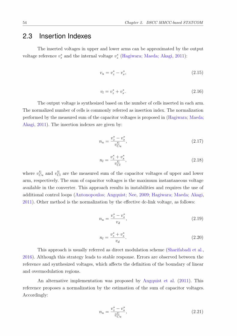
2.3 Insertion Indexes
The inserted voltages in upper and lower arms can be approximated by the output
voltage reference v∗
s and the internal voltage v∗
z (Hagiwara; Maeda; Akagi, 2011):
vu = v∗
z − v∗
s , (2.15)
vl = v∗
z + v∗
s . (2.16)
The output voltage is synthesized based on the number of cells inserted in each arm.
The normalized number of cells is commonly referred as insertion index. The normalization
performed by the measured sum of the capacitor voltages is proposed in (Hagiwara; Maeda;
Akagi, 2011). The insertion indexes are given by:
nu =v∗
z − v∗
s
vΣCu
, (2.17)
nl =v∗
z + v∗
s
vΣCl
, (2.18)
where vΣCu and vΣ
Cl are the measured sum of the capacitor voltages of upper and lower
arm, respectively. The sum of capacitor voltages is the maximum instantaneous voltage
available in the converter. This approach results in instabilities and requires the use of
additional control loops (Antonopoulos; Angquist; Nee, 2009; Hagiwara; Maeda; Akagi,
2011). Other method is the normalization by the effective dc-link voltage, as follows:
nu =v∗
z − v∗
s
vd
, (2.19)
nl =v∗
z + v∗
s
vd
. (2.20)
This approach is usually referred as direct modulation scheme (Sharifabadi et al.,
2016). Although this strategy leads to stable response. Errors are observed between the
reference and synthesized voltages, which affects the definition of the boundary of linear
and overmodulation regions.
An alternative implementation was proposed by Angquist et al. (2011). This
reference proposes a normalization by the estimation of the sum of capacitor voltages.
Accordingly:
nu =v∗
z − v∗
s
vΣCu
, (2.21)

2.4. Dc-link Voltage Design 55
nl =v∗
z + v∗
s
vΣCl
, (2.22)
where vΣCu and vΣ
Cl are the estimation of the sum of capacitor voltages of upper and lower
arm, respectively.
This approach ensures stability in the control of circulating current and the errors
observed between the reference and synthesized voltages can be compensated by the output
current control loops (Sharifabadi et al., 2016). Therefore, the present Master Thesis uses
the approach based on the estimation of the sum of capacitor voltages 3.
2.4 Dc-link Voltage Design
This section presents the design methodology proposed by Cupertino et al. (2018).
The minimum effective dc-link voltage is given by (Fujii; Schwarzer; De Doncker, 2005;
Cupertino et al., 2018):
vd =2√
2√3(1 − ∆vd)
Vs
λmmax
, (2.23)
where λ is the modulation gain, ∆vd is the dc-link voltage ripple and Vs is the minimum
line-to-line voltage (rms) synthesized by the converter. The parameter mmax refers to the
maximum modulation index and can be computed by the carrier frequency fc and the
minimum on-time and dead time Td, as follows (Fujii; Schwarzer; De Doncker, 2005):
mmax =
(1
fc
− 2Td
)fc. (2.24)
In addition, Vs is given by (Fujii; Schwarzer; De Doncker, 2005):
Vs = (1 + ∆Vg)[1 + xeq(pu)(1 + ∆xeq)]Vg, (2.25)
where Vg is the grid voltage, ∆Vg is the grid voltage variation, xeq(pu) is the maximum per
unit value of the output reactance and ∆xeq is the output reactance variation.
The dc-link voltage is an important parameter to avoid overmodulation (Fujii;
Schwarzer; De Doncker, 2005). In order to understand the proposal dc-link voltage design
proposed in (Cupertino et al., 2018), let us consider the ideal waveforms of the Fig. 15.
The reference voltage of the lower arm (vl) is calculated based on (2.16) and (2.25). In
addition, the injection of 16of third harmonic is assumed.
3 The sum of the capacitor voltages estimation will be presented in Chapter 3.

56 Chapter 2. DSCC MMCC-based STATCOM
Figure 15(a) illustrates the ideal waveforms for the dc-link voltage with negligible
ripple when the converter absorbs reactive power. When a voltage ripple is considered in
the dc-link, as illustrated in Fig. 15(b), the converter operates in the overmodulation region.
One solution is to calculate the dc-link voltage considering the ripple ∆vd, as in (2.23).
Therefore, the dc-link voltage value is increased and the converter does not overmodulate,
as shown in Fig. 15(c).
In the reactive power supply region, no overmodulation in the converter is observed
due to the ripple waveform, as shown in Fig. 15(e). Therefore, when considering the same
dc-link voltage value as in reactive power absorption, the result of Fig. 15(f) is obtained.
vd
vd
vd
vd
v,
d
v,
d
Δvd
Δvd
(b) (c)
(d) (e) (f)
Overmodulation
Figure 15 – Qualitative analysis of the effective dc-link voltage design: (a) negligible dc-linkvoltage ripple assuming that the converter absorbs rated reactive power; (b)non-negligible dc-link voltage ripple assuming that the converter absorbsrated reactive power (with overmodulation); (c) non-negligible dc-link voltageripple assuming that the converter absorbs rated reactive power (withoutovermodulation); (d) negligible dc-link voltage ripple assuming that theconverter provides rated reactive power; (e) non-negligible dc-link voltageripple assuming that the converter provides rated reactive power (withoutovermodulation); (f) non-negligible dc-link voltage ripple assuming that theconverter provides rated reactive power (without overmodulation).
As observed, the methodology proposed by Cupertino et al. (2018) is conservative
because it calculates the voltage synthesized by the converter without considering the
operating angle, as in (2.25). Figure 16(a) presents the STATCOM average model and
the phasor diagram is ilustrated in Fig. 16(b). As observed, Vs varies according to the
operating angle of the converter (φ). Equation (2.25) leads to a maximum value of Vs in
the phasor diagram.

2.5. Chapter Conclusions 57
IS
Φ Vg r Ieq S
j xeq SI
Vs
VsVg
reqj xeq
(a)
Is
(b)
Eq. (2.25)
. ..
.
.
. ..
Figure 16 – (a) STATCOM average model; (b) Phasor diagram of STATCOM.
Figure 17 illustrates the output voltage synthesized by the converter depending
on the operating angle. As observed, in the reactive power absorption region, the output
voltage required is less than that calculated by equation (2.25). Therefore, the waveform of
the voltage reference in Figs. 15(a)-(c) should be smaller. In addition, the sum of capacitor
voltages ripple waveform plays an important role in the converter operation. Therefore, a
clear definition of the converter operation limits is very important to define the minimum
voltage control strategy. This analysis will be carried out in chapter 3.
-150 -100 -50 0 50 100 150
Outp
ut
volt
age
( )
ϕ (°)
Vg
V s
Eq. (2.25)
Figure 17 – Output voltage (rms) synthesized by the converter.
2.5 Chapter Conclusions
In this chapter, the topology, dynamic modelling, insertion indexes and DSCC
MMCC design were presented. The basic equations of the DSCC MMCC were derived and

58 Chapter 2. DSCC MMCC-based STATCOM
discussions on the instantaneous powers and their effect on the converter were discussed.
In addition, it was discussed about the stability of the converter that will depend on the
type of normalization performed.
Moreover, other important point is about the dc-link voltage calculation of the
traditional approaches, that does not take into account the waveform of the voltage
reference and the capacitor voltage ripples. This conservative approach leads to higher
values than the necessary depending of the operation conditions. Chapter 3 will discuss
this topic and the minimum voltage control strategy will be derived.

59
3 Minimum Cell Operation Control
This chapter aims to introduce the minimum dc-link voltage operation control.
The potential of bypassing unnecessary cells from the MMCC is presented. In addition, a
sensitivity analysis for cell capacitance and converter reactance is performed. A simplified
analytical power losses model for MMCC, aiming to show the potential for power losses
reduction, is developed. Finally, the limitations of the proposed strategy and implementation
issues are discussed.
3.1 Limits of Linear Modulation Region: Minimum dc-link
Voltage
This section aims to introduce the strategy of minimum dc-link voltage operating,
vd, keeping the converter in the linear region of the modulator. Unlike traditional two-level
converters, MMCC has a non-negligible ripple that limits the maximum output voltage, Vs
(Sharifabadi et al., 2016). The insertion index is limited by the zero voltage, as illustrated
in Fig. 18(a), and the sum of capacitor voltage ripples, as shown in Fig. 18(b), depending
on the operating angle of the output current (Cupertino et al., 2019b).
b( )a( )
Zero voltage
Figure 18 – (a) Insertion index limited by the zero voltage; (b) Insertion index limited bythe sum of capacitor voltage ripples.
For the sake of symmetry, only the lower arm of one phase is analyzed. The internal
voltage reference is given by (Sharifabadi et al., 2016):
v∗
z ≈vd
2, (3.1)
Besides, the third harmonic injection (16pu) is considered to extend the linear

60 Chapter 3. Minimum Cell Operation Control
operation of the converter. Accordingly:
v∗
s = Vs cos(ωnt) −Vs
6cos(3ωnt), (3.2)
where Vs is the output voltage amplitude and ωn is the line fundamental frequency in
rad/s.
In addition, the converter output current is given by:
is = Is cos(ωnt − φ), (3.3)
where Is is the output current amplitude and φ is the displacement angle of the output
current.
Moreover, the estimation of the sum of the capacitor voltages 1 presented in (2.22)
is given by (Angquist et al., 2011):
vΣCl = vd + ∆vΣ
Cl, (3.4)
where ∆vΣCl is the sum of capacitor voltage ripples, given by:
∆vΣCl =
N
2Cvd
(∆WΣ − ∆W∆). (3.5)
∆WΣ and ∆W∆ are given by:
∆WΣ = −VsIs
4ωn
sin(2ωnt − φ) +VsIs
24ωn
sin(2ωnt + φ) +VsIs
48ωn
sin(4ωnt − φ), (3.6)
∆W∆ =vdIs
2ωn
sin(ωnt − φ) −2Vsiz
ωn
sin(ωnt) +Vsiz
9ωn
sin(3ωnt). (3.7)
Finally, iz is given by:
iz =VsIs cos(φ)
2vd
. (3.8)
The output voltage required for grid-connected applications when the converter
injects current (Is) can be computed by inspection of Fig. 10(c), as follows:
Vs =
√[Vg (1 + ∆Vg) + xeq Is sin(φ)
]2+[xeq Is cos(φ)
]2, (3.9)
1 The sum of the capacitor voltage is calculated using the energy stored in the capacitors. The energystored in an upper arm is given by
∫vu × iu
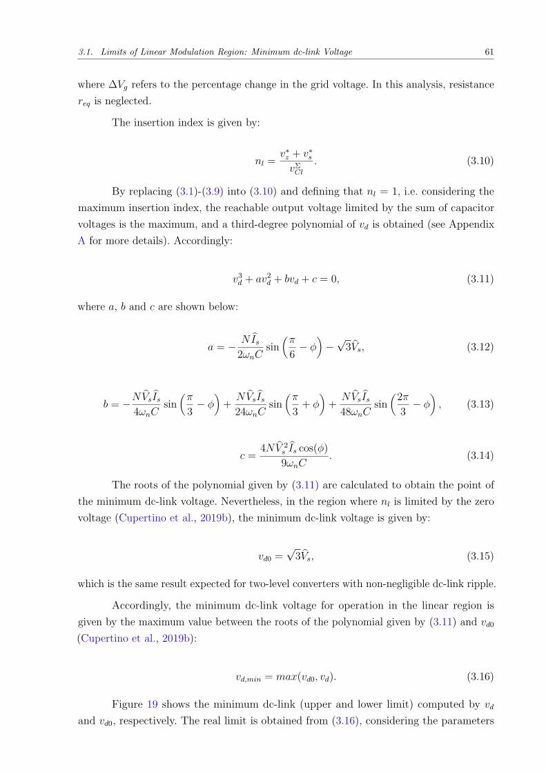
3.1. Limits of Linear Modulation Region: Minimum dc-link Voltage 61
where ∆Vg refers to the percentage change in the grid voltage. In this analysis, resistance
req is neglected.
The insertion index is given by:
nl =v∗
z + v∗
s
vΣCl
. (3.10)
By replacing (3.1)-(3.9) into (3.10) and defining that nl = 1, i.e. considering the
maximum insertion index, the reachable output voltage limited by the sum of capacitor
voltages is the maximum, and a third-degree polynomial of vd is obtained (see Appendix
A for more details). Accordingly:
v3d + av2
d + bvd + c = 0, (3.11)
where a, b and c are shown below:
a = −NIs
2ωnCsin
(π
6− φ
)−
√3Vs, (3.12)
b = −NVsIs
4ωnCsin
(π
3− φ
)+
NVsIs
24ωnCsin
(π
3+ φ
)+
NVsIs
48ωnCsin
(2π
3− φ
), (3.13)
c =4NV 2
s Is cos(φ)
9ωnC. (3.14)
The roots of the polynomial given by (3.11) are calculated to obtain the point of
the minimum dc-link voltage. Nevertheless, in the region where nl is limited by the zero
voltage (Cupertino et al., 2019b), the minimum dc-link voltage is given by:
vd0 =√
3Vs, (3.15)
which is the same result expected for two-level converters with non-negligible dc-link ripple.
Accordingly, the minimum dc-link voltage for operation in the linear region is
given by the maximum value between the roots of the polynomial given by (3.11) and vd0
(Cupertino et al., 2019b):
vd,min = max(vd0, vd). (3.16)
Figure 19 shows the minimum dc-link (upper and lower limit) computed by vd
and vd0, respectively. The real limit is obtained from (3.16), considering the parameters

62 Chapter 3. Minimum Cell Operation Control
of Table 5. As observed, the required dc-link voltage varies according to the operation
angle of the output current, with critical condition when the converter absorbs reactive
power. In addition, the nominal dc-link voltage (vdn) adopted is 24.5 kV, which meets the
requirement for all operating points.
Table 5 – Parameters of the DSCC MMCC-based STATCOM.
Parameter Value
Grid voltage (Vg) 13.8 kV
Rated power (Sn) 17 MVA
Transformer inductance (Lf ) 1.4 mH
Transformer X/R ratio 18
Arm inductance (Larm) 3 mH
Arm inductor X/R ratio 17
Cell capacitance (C) 7.1 mF
Nominal cell voltage (v∗
cell) 942 V
Line frequency (fn) 60 Hz
Sampling frequency (fsw) 10.92 kHz
Number of cells (N) 26 per arm
vd vd0 Real Limit
15
20
25
ϕ(°)
-180 -150 -100 -50 0 50 100 150 180
vd
(kV
)
Absorbs Reactive Power
Provides Reactive Power
8.74 %
Figure 19 – Minimum dc-link voltage for operation in the linear region of the modulatoras function of the operating angle of the output current (parameters in Table5).
The region where STATCOM absorbs reactive power from the grid is represented
by the phasor diagram of Fig. 20(a). As can be seen, the current is leading with the
voltage and therefore, the reactive power is negative (Q < 0). The region where STATCOM
provides reactive power to the grid is represented by the phasor diagram of Fig. 20(b). In
this condition, the current is lagging with the voltage and therefore the reactive power is
positive (Q > 0).
Moreover, due to output current Is variation, and consequent injection of reactive
power, changes are observed in the curve of the minimum dc-link voltage, as shown in Fig.
21. The effect of the output current is higher in the reactive power absorption region.
In conclusion, a difference superior to 8% is observed between the voltages required
under the conditions in which the converter absorbs and provides reactive power. Such

3.2. Analysis of the Minimum Cell Operation Control 63
(a)
ISΦ
Vg
r Ieq S
j xeq SIVs
(b)
. .
.
..
IS
Φ
Vg
r Ieq S
j xeq SIVs
. .
.
..
Φ = 90 ° Q > 0Φ = -90 ° Q < 0
Figure 20 – Phasor diagram of STATCOM (a) absorbing reactive power; (b) providingreactive power. Remark: is = Is cos(ωnt − φ).
-180 -150 -100 -50 0 50 100 150 180
20
25
vd
(kV
)
ϕ (°)
Isn I0.8 sn I0.6 sn I0.4 sn I0.2 sn I0 sn
Figure 21 – Minimum dc-link voltage as function of the operating angle of the outputcurrent and the current output Is (parameters in Table 5).
difference indicates that, in the reactive power supply region, less cells are required and an
efficiency gain is expected for this region by bypassing such cells.
As a way of comparison, in two-level converters, the biggest dc-link voltage
requirement occurs in the region where the converter provides reactive power to the
grid. This is because the ripple of the capacitor voltage for this topology is negligible.
3.2 Analysis of the Minimum Cell Operation Control
3.2.1 Potential of Bypassing Unnecessary Cells
This section presents the potential of bypassing unnecessary cells from the DSCC
MMCC, according to the reactive power profile to be compensated. In addition, a sensitivity
analysis for cell capacitance and converter reactance is performed.
The analyses are focused on the STATCOM operation. Therefore, φ = ±90 is
employed. Under such conditions, the required dc-link voltage can be evaluated according
to the injected reactive power. Fig. 22(a) shows the minimum dc-link variation as function
of the cell capacitance. As observed, vd is more affected in the region when the converter
absorbs reactive power. Fig. 22(b) presents variation as function of the converter reactance.

64 Chapter 3. Minimum Cell Operation Control
As noted, xeq affects both regions. This means that the change in the inverter parameters
affects the potential of bypass cells.
20
25
vd
(kV
)
-1 -0.8 -0.6 -0.4 -0.2 0 0.2 0.4 0.6 0.8 1
(a)
0.9C 1.1CC
20
25
vd
(kV
)
-1 -0.8 -0.6 -0.4 -0.2 0 0.2 0.4 0.6 0.8 1
( )b
Reactive power [pu]
0.8x eq 1.2x eqxeq
Figure 22 – Minimum dc-link voltage as function of the operating reactive power and (a)cell capacitance variation, (b) output reactance variation.
Alternatively, the reactance and capacitance variations can be evaluated based on
the analysis of the minimum cell operation according to the operating reactive power. For
such, the number of unnecessary cells is defined as:
Nf = floor
(vdn − vd
v∗
cell
), (3.17)
where vdn is the nominal dc-link voltage, vd is the dc-link voltage required in each operating
condition and v∗
cell is the nominal cell voltage.
Figure 23 is obtained considering the parameters of Table 5 and equation (3.17). As
observed, the number of unnecessary cells varies according to the reactive power. Moreover,
Fig. 23(a) reveals variation in the reactive power absorption region with cell capacitance
change, where the insertion index is limited by the sum of the capacitor voltage waveforms.
Fig. 23(b) shows variation in both operations with the xeq, since it affects the insertion
index by the limitations of sum of capacitor voltage waveforms and zero voltage.
3.2.2 Potential to Reduce Conduction Losses
This section presents a simplified analytical power losses model for DSCC MMCC,
aiming to show the potential for power losses reduction. Only the semiconductor conduction
losses are evaluated, since these losses are dominant in MMCC (Sharifabadi et al., 2016).
The following assumptions are considered:

3.2. Analysis of the Minimum Cell Operation Control 65
(a)-1 -0.8 -0.6 -0.4 -0.2 0 0.2 0.4 0.6 0.8 1
0
1
2
3
45
0.9C 1.1CC
Nf
0.8x eq 1.2x eqxeq
0
1
2
3
45
Nf
( )b
-1 -0.8 -0.6 -0.4 -0.2 0 0.2 0.4 0.6 0.8 1
Reactive power [pu]
Figure 23 – Number of unnecessary cells as function of the operating reactive power and(a) cell capacitance variation, (b) reactance variation.
• The modulation signals are ideal;
• The high frequency content present in the currents is negligible;
• Delays and non-idealities present in the modulation process are negligible;
• The losses are evenly distributed to the converter cells.
The conduction losses can be estimated by (Anurag; Yang; Blaabjerg, 2015):
Pcond,x = Vxix,avg + rxi2x,rms, (3.18)
where ix,avg and ix,rms indicates the average and rms current values in the switch x (S1,
S2, D1 or D2). Vx represents the collector-emitter voltage for the IGBT and the forward
voltage for the diode.
Therefore, the average and rms currents in each semiconductor switch are necessary
to estimate the conduction losses. Due to symmetry, only the upper arm is analyzed.
Considering the upper arm current positive, the devices S2 and D1 are capable of conducting,
and the average currents are given by (Bakhshizadeh et al., 2015):
iS2,avg =1
2π
(∫ θz,1
0muiudθ +
∫ 2π
θz,2
muiudθ
), (3.19)
iD1,avg =1
2π
(∫ θz,1
0muiudθ +
∫ 2π
θz,2
muiudθ
). (3.20)

66 Chapter 3. Minimum Cell Operation Control
Considering the upper arm current negative, the devices S1 and D2 are capable of
conducting, and the average currents are given by:
iS1,avg =1
2π
(∫ θz,2
θz,1
−muiudθ
), (3.21)
iD2,avg =1
2π
(∫ θz,2
θz,1
−muiudθ
). (3.22)
The current iu is given by:
iu = iz +Is
2cos(θ − φ), (3.23)
where θ = ωnt.
The angles θz,1 and θz,2 define the arm current zero-crossings given by:
θz,1 = π − φ − cos−1
(mi cos(φ)
2
), (3.24)
θz,2 = π − φ + cos−1
(mi cos(φ)
2
), (3.25)
where mi is the modulation index. For STATCOM operation, φ = ±90 is considered. In
addition, the circulating current iz is negligible.
mu is the ideal modulation signal of upper arm and mu = 1 − mu, as follows
(Sharifabadi et al., 2016):
mu =1
2−
mi
2cos(ωnt) +
mi
12cos(3ωnt). (3.26)
Replacing equations (3.23) and (3.26) in relations (3.19)-(3.22) and performing the
integration leads to:
iS1,avg = iS2,avg = iD1,avg = iD2,avg =Is
4π. (3.27)
By following the same reasoning, the rms currents of the semiconductor devices
are given by:
iS2,rms =
√√√√ 1
2π
(∫ θz,1
0mui2
udθ +∫ 2π
θz,2
mui2udθ
), (3.28)

3.2. Analysis of the Minimum Cell Operation Control 67
iD1,rms =
√√√√ 1
2π
(∫ θz,1
0mui2
udθ +∫ 2π
θz,2
mui2udθ
), (3.29)
iS1,rms =
√√√√ 1
2π
(∫ θz,2
θz,1
−mui2udθ
), (3.30)
iD2,rms =
√√√√ 1
2π
(∫ θz,2
θz,1
−mui2udθ
). (3.31)
By solving equations (3.28)-(3.31), the rms currents of the semiconductor devices
are obtained as follows:
iS1,rms = iS2,rms = iD1,rms = iD2,rms =Is
4√
2. (3.32)
Replacing (3.27) and (3.32) in equation (3.18) leads to:
Pcond,x = Vx
Is
4π+ rx
(Is
4√
2
)2
. (3.33)
As noted in this simplified model, conduction losses do not depend on the modulation
index in the STATCOM operation. The total conduction losses in the MMCC can be
estimated based on the losses on the devices of a cell and multiplied by the number of
operating cells. Therefore, the conduction losses in the DSCC MMCC are given by:
Pcond,MMC = 6(N − Nf )(Pcond,S1 + Pcond,S2 + Pcond,D1 + Pcond,D2). (3.34)
Accordingly, the potential for reducing conduction losses is given by the percentage
of cells that are bypassed. For the parameters of Table 5, when the STATCOM operates at
hot-standby, Nf = 4 and conduction losses are reduced by 426
= 15.38 %. When STATCOM
provides rated reactive power, Nf = 2 and the conduction losses are reduced by 226
= 7.69
%. When STATCOM absorbs rated reactive power, Nf = 0 and conduction losses are
reduced by 026
= 0 %, i.e. no reduction is observed.
The total MMCC power losses include the inductor losses and also the semiconductor
switching losses. Therefore, the perceptual losses reduction presented in this section is an
upper boundary for the real reduction. The real reduction also depends on the employed
mission profile.

68 Chapter 3. Minimum Cell Operation Control
3.3 Limitations
This section aims to present the limitations of the minimum cell operation control.
Two topics are approached:
1. In MMCCs with few number of cells, the cell voltage represents a significant part of
the dc-link voltage. Under such conditions, the cell bypass may not be possible. This
section aims to compute the minimum number of cells Nmin which guarantees that
the proposed strategy is suitable for power losses reduction;
2. When the converter is operating at low current (e.g. hot standby) and the current
reference increases, cells must be inserted in the main circuit. However, these cells may
be discharged. Under such conditions, the converter will operate in the overmodulation
region during transients and stability problems might arise. This section also computes
the maximum number of cells Nf,max which can be bypassed without affecting the
converter stability.
3.3.1 Minimum number of cells Nmin
For simplification reasons, the regions where STATCOM absorbs and provides
reactive power are evaluated separately. In the reactive power absorption region, the
maximum output voltage is limited by the sum of capacitor voltages, as illustrated in Fig.
18(b). Under such conditions, the following equation can be written for the lower arms:
vd,abs
2+ v∗
s,abs ≤ vΣCl, (3.35)
where vd,abs and v∗
s,abs are the required dc-link voltage and output voltage when the
STATCOM absorbs rated reactive power, respectively. Assuming that the converter is
designed to operate in the boundary of the linear region, the maximum output voltage
can be roughly estimated by:
vd,abs
2+ max(v∗
s,abs) ≤ vd,abs(1 − ∆V ) → max(v∗
s,abs) ≈ vd,abs
(1
2− ∆V
), (3.36)
where ∆V is the ripple (average to minimum) of the sum of the capacitor voltages at rated
reactive current.
Under hot standby conditions (reference current equals to zero), the equation (3.36)
can be rewritten as:
max(v∗
s,0) =vd,0
2, (3.37)

3.3. Limitations 69
where vd,0 and v∗
s,0 are the required dc-link voltage and output voltage at hot standby,
respectively. As observed, a negligible voltage ripple was assumed, when Is = 0. Dividing
(3.37) by (3.36) yields:
vd,0
vd,abs
≈ (1 − 2 · ∆V )max(v∗
s,0)
max(v∗
s,abs). (3.38)
In the reactive power supply region, the maximum output voltage is limited by the
dc-link voltage. Under such conditions, the following equation can be written for the lower
arms:
vd,prov
2+ v∗
s,prov ≤ vΣCl, (3.39)
where vd,prov and v∗
s,prov are the required dc-link voltage and output voltage when the
STATCOM provides rated reactive power, respectively. By assuming that the converter is
designed to operate in the limit of the linear region, the maximum output voltage can be
roughly estimated by:
vd,prov
2+ max(v∗
s,prov) ≤ vd,prov → max(v∗
s,prov) ≈vd,prov
2, (3.40)
Dividing (3.37) by (3.40) yields:
vd,0
vd,prov
≈max(v∗
s,0)
max(v∗
s,prov). (3.41)
At this point, typical values are adopted. Assuming the converter equivalent output
impedance lower than 10 % leads to:
max(v∗
s,0)
max(v∗
s,abs)≤
1
1 − 0.1< 1.12, (3.42)
max(v∗
s,0)
max(v∗
s,prov)≤
1
1 + 0.1< 0.91. (3.43)
Finally, by assuming ∆V ≤ 10%, the following relations can be obtained:
vd,0
vd,abs
≈ (1 − 2 × 0.1) × 1.12 = 0.896, (3.44)
vd,0
vd,prov
≈ 0.91. (3.45)
Since the number of cells must be integer, cells can be bypassed for reactive power
absorption operation only if the cell voltage reference is lower than 10 % of the total

70 Chapter 3. Minimum Cell Operation Control
dc-link voltage. For reactive power supply operation, the cell voltage reference is lower
than 9 % of the total dc-link voltage. These conclusions were obtained considering typical
values adopted in MMCC design (Sharifabadi et al., 2016). This means that the proposed
technique is applicable for MMCCs with a number of cells higher than Nmin = 10.
3.3.2 Maximum number of bypassed cells Nf,prov and Nf,abs
When the STATCOM reactive power reference decreases, the capacitor voltage
ripple decreases and the required output voltage changes (it increases for reactive power
supply operation and decreases for reactive power absorption operation). Under such
conditions, some cells can be bypassed, since the STATCOM presents higher voltage
synthesis capability than necessary. Once the number of bypassed cells is computed to
guarantee the operation in the linear region, no stability issues are expected during the
bypass process. On the other hand, during the insertion process, the converter is expected
to operate in the overmodulation region during transients. This fact is observed because
the STATCOM presents lower voltage synthesis capability than necessary (some cells were
previously bypassed). Since the voltage gain provided by the overmodulation region is
limited, some stability issues may arise.
References (Hava; Kerkman; Lipo, 1998; Hava et al., 1999) discussed the operation
of voltage source converters in the overmodulation region during steady-state and transients.
These concepts can be extended to the MMCC operation, leading to acceptable transients,
as discussed in references (Lopez et al., 2015; Briff; Moreno; Chivite-Zabalza, 2017). A
rough estimation of the maximum number of cells which can be bypassed to avoid stability
issues in the insertion process is presented as follows.
Indeed, the converter can synthesize 10 % more output voltage in the overmodulation
region, i.e., the maximum modulation gain is Λmax = 1.1. The worst operational case is
taken into account: a step in the reference from zero to the rated reactive power. During
the delay and the charging process of the inserted cells, the stability must be guaranteed.
Figure 24 presents a qualitative analysis of the MMCC during the insertion process.
Figure 24 (a) shows the sum of capacitor voltages (vΣCl) and the reference voltage of the
lower arm (vl) at hot standby operation. When the converter reference is changed from
0 to 1 pu (reactive power supply operation), the reference voltage increases, since the
required output voltage must be higher, as observed in Fig. 24 (b). Under such conditions,
the overmodulation is observed in the highlighted areas and the required increase in
the reference voltage must be available in the overmodulation region. If the converter is
designed to operate in the limit of the linear region in steady-state, as shown in Figs. 24
(a) and (c), this means that:

3.3. Limitations 71
(b) (c)
(d) (e) (f)
d,0
d,0
d,0
d,0
d,prov
d,abs
Figure 24 – Qualitative analysis of the DSCC MMCC-based STATCOM operation duringthe insertion transient: (a) Ideal waveforms for hot standby operation; (b)Ideal waveforms for operation in overmodulation region for rated reactivepower supply operation (before insertion); (c) Ideal waveforms for operationfor rated reactive power supply operation (after insertion); (d) Ideal waveformsfor hot standby operation; (e) Ideal waveforms for operation in overmodulationregion for rated reactive power absorption operation (before insertion); (f)Ideal waveforms for operation for rated reactive power absorption operation(after insertion).
vd,prov
vd,0
≤ Λmax. (3.46)
Relation (3.46) determines the maximum voltage difference between hot standby
and full reactive power supply operation. Accordingly, the maximum number of cells which
can be bypassed Nf,prov is estimated by:
Nf,prov ≤ (Λmax − 1)N. (3.47)
Figure 24 (d) shows the sum of capacitor voltages and the reference voltage of
the lower arm at hot standby operation, which was repeated for visualization reasons.
When the converter reference is changed from 0 to 1 pu of reactive power absorption
operation, the reference voltage decreases, since the required output voltage must be lower,
as observed in Figure 24 (e). Under such conditions, the overmodulation is observed in the
highlighted areas. If the converter is designed to operate in the limit of the linear region in

72 Chapter 3. Minimum Cell Operation Control
steady-state, as shown in Figs. 24 (d) and (f), this means that:
vd,abs(1 − ∆V )
vd,0
≤ Λmax →vd,abs
vd,0
≤Λmax
1 − ∆V. (3.48)
Therefore, the maximum number of cells which can be bypassed Nf,abs is given by:
Nf,abs ≤(
Λmax
1 − ∆V− 1
)N. (3.49)
At this point, the following conclusions can be stated:
• In the reactive power supply region, the maximum number of cells which can be
bypassed is 10 % of the total;
• In the reactive power absorption region, more cells can be bypassed. Considering
∆V = 10 %, the maximum number of cells which can be bypassed is 22 % of the
total, according to equation (3.49);
• For example, if N = 26, Nf,prov ≤ 2.6 and Nf,abs ≤ 5.7.
As observed in Fig. 23, 2 cells were bypassed in the reactive power supply region,
while 4 were bypassed in the reactive power absorption region, in the case study adopted
(N = 26), which are within the stability limits derived in this section. It is important to
remark that the results presented in this section are rough approximations and must be
interpreted as static stability limits. Therefore, some margin must be adopted due to the
current control dynamics.
3.4 Bypass and Insertion Procedures
When plastic IGBT modules (PIM) are used, the bypass structure is based on a
thyristor connected in parallel with a vacuum contactor, as illustrated in Fig. 12. The
thyristor provides a fast bypass when compared to the vacuum contactor. However, the
conduction losses of the vacuum contactor are negligible, which justifies its application
(Wang et al., 2017).
Figure 25 illustrates the cell bypass and insertion procedures. In the bypass
procedure, contactor ST and thyristor T receive power-up signal at time t1. In addition,
the thyristor presents 1 ms delay and the contactor has a maximum closing time of 60
ms (SIEMENS, 2019a). In the conduction period of T , the arm current is assumed. At
the time t2, the bypass mode is initialized, where ST is conducted and the cell is removed
from the main circuit of MMCC.

3.5. Chapter Conclusions 73
TS
T
60 ms
Normal
t1 t2 t3 t4
60 ms
1 ms 1 ms
! !
! !
OperationBypass
ProcedureBypassMode
InsertionProcedure
NormalOperation
!
! !
!
!
!
Figure 25 – Conduction states of the bypass switch elements during the bypass andinsertion procedures. The maximum delay of the contactor is assumed to beequal to 60 ms for both turn-on and turn-off.
On the other hand, in the insertion procedure, contactor ST receives power-off
signal and thyristor T receives power-up signal at time t3. At the time t4, the normal
operation is initialized, where ST and T stop driving and the cell is inserted into the main
circuit of MMCC.
3.5 Chapter Conclusions
In this chapter the minimum cell operation control strategy was proposed. Analytical
expressions of the proposed technique potential were derived and its application limits
were evaluated. These results indicated that the proposed technique can be applied for a
DSCC MMCC-based STATCOMs with more than 10 cells and does not require additional
hardware. Furthermore, during the insertion of cells, the converter can operate in the
overmodulation region. Therefore, there is a maximum number of cells which can be
bypassed, due to stability reasons.
In the next chapter, the control strategy and the tuning of the controllers will be
discussed. In addition, the system parameters will be presented.


75
4 Control Strategy and Control Tuning
This chapter introduces the control strategy employed and the control tuning for an
DSCC MMCC-based STATCOM. First of all, some popular control structures are briefly
described. Then, the selected control strategy is discussed in details and the control tuning
procedure is derived.
4.1 Control Strategies
The control objectives of the MMCC are based on the control of the total energy of
the converter, control of the circulating current, balancing of the capacitors and injection
of reactive power in the grid. This section discusses three popular control schemes for
DSCC MMCC.
4.1.1 Direct voltage control
The direct voltage control scheme is presented in Fig. 26. Originally, this scheme
does not present a circulating current suppression control, which leads to high circulating
currents in the converter (Siemaszko et al., 2010). A direct voltage control combined with
circulating current control is presented by (Sharifabadi et al., 2016).
The normalization of the insertion indexes are given by the effective dc-link voltage
vd. Accordingly:
nu =v∗
z − v∗
s
vd
, (4.1)
nl =v∗
z + v∗
s
vd
. (4.2)
As advantages, the direct modulation scheme is inherently asymptotically stable
(Siemaszko et al., 2010; Harnefors et al., 2013). This means that the arm voltages reach
the reference value (vd
N) without any additional energy balancing controller. However,
as discussed in Chapter 2, errors are observed between the reference and synthesized
voltages, which affects the definition of the boundary of linear and overmodulation regions.
Therefore, this strategy is not employed in this Master Thesis.

76 Chapter 4. Control Strategy and Control Tuning
Circulatingcurrentcontrol
Outputcurrentcontrol
Globalenergycontrol
WT* Instantaneous
power theory
P*
Q*
isα*
isβ*
vgα vgβ
iz,n*
abc
αβ
vsα*
vsβ*
vs,n*
vz,n*
Figure 26 – Direct voltage control of a DSCC MMCC-based STATCOM.
4.1.2 Closed-loop voltage control
The closed-loop voltage control scheme is presented in Fig. 27. The normalization
of the insertion indexes are given by the measured sum of the capacitor voltages vΣC .
Accordingly:
nu =v∗
z − v∗
s
vΣCu
, (4.3)
nl =v∗
z + v∗
s
vΣCl
. (4.4)
Leg energybalancing
control
Arm energybalancing
control
Circulatingcurrentcontrol
Outputcurrentcontrol
Globalenergycontrol
WT* Instantaneous
power theory
P*
Q*
isα*
isβ*
ΔWΣ,n*
ΔWΔ,n*
vgα vgβ
izdc,n*
izac,n*
iz,n*
abc
αβ
vsα*
vsβ*
vs,n*
vz,n*
Figure 27 – Closed-loop voltage control of a DSCC MMCC-based STATCOM.
In this strategy, the definition of boundary between the linear and overmodulation
regions is straightforward, since the sum of capacitor voltages is the instantaneous available

4.1. Control Strategies 77
dc voltage for output voltage synthesis. However, two additional arm energy balancing
controllers are included in the control scheme. These structures are needed to guarantee
the asymptotic stability of the arm voltages (Siemaszko et al., 2010; Sharifabadi et al.,
2016). Due to its higher complexity, this scheme is not used in this Master Thesis.
4.1.3 Open-loop voltage control
Finally, the open-loop voltage control scheme is presented in Fig. 28. Instead of
using the measurement of the sum of capacitor voltages, the normalization of the insertion
indexes are based on the estimation of the sum of the capacitor voltages vΣC . Accordingly:
nu =v∗
z − v∗
s
vΣCu
, (4.5)
nl =v∗
z + v∗
s
vΣCl
. (4.6)
Circulatingcurrentcontrol
Outputcurrentcontrol
Globalenergycontrol
WT* Instantaneous
power theory
P*
Q*
isα*
isβ*
vgα vgβ
iz,n*
abc
αβ
vsα*
vsβ*
vs,n*
vz,n*
Figure 28 – Open-loop voltage control of a DSCC MMCC-based STATCOM.
Assuming that the sum of capacitor voltages are correctly estimated, this control
strategy allows a clear definition of the boundary between linear and overmodulation
regions. In addition, this strategy is asymptotically stable without any additional energy
balancing controller (Antonopoulos et al., 2014; Harnefors et al., 2015). Therefore, this
control strategy is employed in this Master Thesis and it is described in the following
paragraphs.
The control strategy adopted in this work is illustrated in Fig. 29, with N0 =
6(N −Nf ). The output and circulating currents are controlled through resonant controllers
in stationary reference frame (Farias et al., 2018). The circulating current control supress
the harmonics in the circulating current and inserts damping in the converter dynamic
response (Yue et al., 2016).

78 Chapter 4. Control Strategy and Control Tuning
InstantaneousPower Theory
P
Q
*
*
vgαvgβ isα
isβ
vgα
vgβ
αβ
abcPR
PR
iu1/2
il
LPF
Rarm
izPR
vs
vz
isα*
isβ*
*
*
iu
il
is αβ
abc
isα
isβ
vg
vgα
vgβ
/12N
DSOGI -
PNSE
Output Current Control
PI
TW
WT*
Σ
( )2
MAF
vcell
C20
( )2
vcell
d
*
1/N
Global Energy Circulating Current Control
N0
v
Control
N
P*
dv
Figure 29 – Complete control strategy of a DSCC MMCC-based STATCOM.
The global energy control indirectly reduces the dc-link voltage during the bypass
of unnecessary cells from the converter. This controller computes the active power reference
P ∗, as follows (Cupertino et al., 2019b):
P ∗ =
(kp,W +
ki,W
s
)
1
2C · 6(N − Nf ) ·
(vd
N
)2
︸ ︷︷ ︸W ∗
T
−1
2C ·
6(N−Nf )∑
i=1
v2cell,i
︸ ︷︷ ︸WT
, (4.7)
where W ∗
T is the desired energy storage, WT is the total energy storage, vcell,i is the i-th
cell voltage of the converter and kp,W and ki,W refer to the proportional and integral gains
of the energy controller.
The output current references is computed by Instantaneous Power Theory (Akagi;
Watanabe; Aredes, 2007), given by (4.8). The output current is controlled through resonant
controllers in stationary reference frame (Farias et al., 2018).
i∗
sα
i∗
sβ
=
1
(vgα)2 + (vgβ)2
vgα vgβ
vgβ −vgα
P ∗
Q∗
, (4.8)
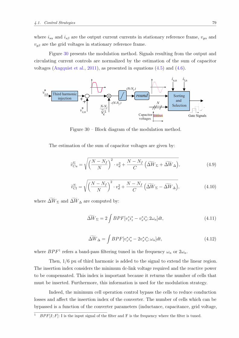
4.1. Control Strategies 79
where isα and isβ are the output current currents in stationary reference frame, vgα and
vgβ are the grid voltages in stationary reference frame.
Figure 30 presents the modulation method. Signals resulting from the output and
circulating current controls are normalized by the estimation of the sum of capacitor
voltages (Angquist et al., 2011), as presented in equations (4.5) and (4.6).
N-Nf
(N-Nf )
-(N- )Nf
round
vcΣ
Capacitorvoltages
N
Sorting
and
Selection
Gate Signals
~
vs,n*
Third harmonicinjection
vz,n*
iu,n il,n
Figure 30 – Block diagram of the modulation method.
The estimation of the sum of capacitor voltages are given by:
vΣCu =
√(N − Nf
N
)2
· v2d +
N − Nf
C
(∆W Σ + ∆W ∆
), (4.9)
vΣCl =
√(N − Nf
N
)2
· v2d +
N − Nf
C
(∆W Σ − ∆W ∆
), (4.10)
where ∆W Σ and ∆W ∆ are computed by:
∆W Σ = 2∫
BPF [v∗
z i∗
z − v∗
s i∗
s; 2ωn]dt, (4.11)
∆W ∆ =∫
BPF [v∗
z i∗
s − 2v∗
s i∗
z; ωn]dt, (4.12)
where BPF 1 refers a band-pass filtering tuned in the frequency ωn or 2ωn.
Then, 1/6 pu of third harmonic is added to the signal to extend the linear region.
The insertion index considers the minimum dc-link voltage required and the reactive power
to be compensated. This index is important because it returns the number of cells that
must be inserted. Furthermore, this information is used for the modulation strategy.
Indeed, the minimum cell operation control bypass the cells to reduce conduction
losses and affect the insertion index of the converter. The number of cells which can be
bypassed is a function of the converter parameters (inductance, capacitance, grid voltage,
1 BPF [I; F ]: I is the input signal of the filter and F is the frequency where the filter is tuned.

80 Chapter 4. Control Strategy and Control Tuning
current, etc.). In this sense, it is important to remark that the proposed approach can be
applied for different modulation strategies.
In this work, the Nearest Level Control (NLC) is used, with the adoption of the
cell tolerance band algorithm (Hassanpoor; Norrga; Nami, 2015). This approach has
some advantages such as not requiring offline computing (as in SHE PWM techniques)
and possibility of implementation in Field Programmable Gate Array (FPGA) (reducing
implementation efforts) (Sharifabadi et al., 2016). Due to the sorting and selection algorithm,
the capacitor voltage balance is inherently achieved. The switching losses are reduced in
comparison with carrier-based strategies because the switching events happen only when
the capacitor voltages reach the tolerance band (Hassanpoor; Norrga; Nami, 2015).
4.2 Control Tuning
This section describes the control tuning of the control strategy presented in section
4.1. Three controls are addressed: output current control, circulating current control and
global energy control.
4.2.1 Output current control
Figure 31 presents the block diagram of the output current control. DI(s) is the
compensator transfer function, given by:
DI(s) = kp,I +kr,Is
s2 + ω2n
, (4.13)
where kp,I and kr,I refer to the proportional and resonant gains of the output current
controller. The resonant controller tuned in the fundamental harmonic is employed. GD(s)
represents the model of the Pulse Width Modulation (PWM) modulator and the delay
caused by the digital implementation. The PWM processing delay can be approximated
by a zero-order hold (zoh) function and the implementation delay by one sample delay.
Hence, the total delay in the control loop will be 1.5Tsw (Yao et al., 2017). Accordingly:
GD(s) =1 − e−Tsw
Tswse−Tsw ≈
1
1.5Tsws + 1, (4.14)
where Tsw is the sampling time.
The plant function of the output current controller GI(s) is given by:
GI(s) =1
sLeq + Req
. (4.15)

4.2. Control Tuning 81
isαβ (s)*
D (s)I
isαβ (s)
GD (s) GI (s)
vgαβvgαβ
Figure 31 – Block diagram of the output current control.
In addition, the open-loop transfer function for the control scheme is given by:
Gi(s) = DI(s) · GD(s) · GI(s). (4.16)
Replacing (4.13)-(4.15) in (4.16), the transfer function of (4.16) can be expressed
as:
Gi(s) =
(kp,I +
kr,Is
s2 + ω2n
)·(
1
1.5Tsws + 1
)·(
1
sLeq + Req
). (4.17)
Considering the methodology proposed by Holmes et al. (2009) for maximize the
control bandwidth, the following gains for the proportional resonant (PR) controller is
obtained:
kp,I =π2
− φm
1.5Tsw
Leq, (4.18)
kr,I =π2
− φm
15Tsw
kp,I , (4.19)
where φm is the desired phase margin (e.g. 85) (Holmes et al., 2009).
4.2.2 Circulating current control
Figure 32 presents the block diagram of the circulating current control. DZ(s) is
the compensator transfer function, given by:
DZ(s) = kp,Z +kr,Zs
s2 + 4ω2n
, (4.20)
where kp,Z and kr,Z refer to the proportional and resonant gains of the circulating current
controller. The resonant controller tuned in the second harmonic is employed to eliminate
the second harmonic component present in the circulating current. GD(s) represents the
implementation delay given by equation (4.14).

82 Chapter 4. Control Strategy and Control Tuning
The plant function of the circulating current controller GZ(s) is given by:
GZ(s) =1
sLarm + Rarm
. (4.21)
izαβ (s)*
D (s)Z
izαβ (s)
GD (s) GZ (s)
vd
2
vd
2
Figure 32 – Block diagram of the circulating current control.
Furthermore, the open-loop transfer function for the control scheme is given by:
Giz(s) = DZ(s) · GD(s) · GZ(s). (4.22)
Replacing (4.20), (4.15) and (4.21) in (4.22), the transfer function of (4.22) can be
expressed as:
Giz(s) =
(kp,Z +
kr,Zs
s2 + ω2n
+kr,Zs
s2 + 4ω2n
)·(
1
1.5Tsws + 1
)·(
1
sLarm + Rarm
). (4.23)
Considering the methodology proposed by Holmes et al. (2009), the following gains
for the PR controller is obtained:
kp,Z =π2
− φm
1.5Tsw
Larm, (4.24)
kr,Z =π2
− φm
15Tsw
kp,Z . (4.25)
4.2.3 Global energy control
The block diagram of the global energy control is illustrated in Fig. 33. W ∗
T is
calculated by:
W ∗
T =6N∑
i=1
1
2Cv2
cell,i =1
2·(
6C
N
)· v2
d. (4.26)
DW (s) is the compensator transfer function, given by:
DW (s) = kp,W +ki,W
s, (4.27)

4.2. Control Tuning 83
where kp,W and ki,W refer to the proportional and integral gains of the global energy
controller. Gm(s) represents the dynamics of a moving average filter (MAF) used to
attenuate the low frequency of the capacitor voltage, which can insert oscillations in the
control. Gm(s) can be approximated by:
Gm(s) =1
0.25Tms + 1, (4.28)
where Tm = 1fm
. fm is the frequency of the capacitor voltage ripple (i.e. 60 Hz in this
work).
The plant function of the global energy controller GW (s) is given by:
GW (s) =1
s. (4.29)
WT (s)*
D (s)Woutput current control
GW (s)
WT (s)
loop (gain 1)≈
Gm (s)
P* P
Figure 33 – Block diagram of the global energy control.
Moreover, the open-loop transfer function for the control scheme is given by:
Gw(s) = DW (s) · Gm(s) · GW (s). (4.30)
Replacing (4.27)-(4.29) in (4.30), the transfer function of (4.30) can be expressed
as:
Gw(s) =
(kp,W +
ki,W
s
)·(
1
0.25Tms + 1
)·(
1
s
). (4.31)
Considering symmetrical optimum method proposed by Teodorescu, Liserre and
Rodriguez (2011), the following gains for the PI controller is obtained:
kp,W =1.65
Tm
, (4.32)
ki,W =1.14
T 2m
, (4.33)
which leads to a phase margin of 45.

84 Chapter 4. Control Strategy and Control Tuning
4.3 Chapter Conclusions
In this chapter three control strategies used in DSCC MMCC is presented and their
stability is discussed. The control strategy employed and tuning of the controllers were
presented. In the next chapter the case studies and system parameters will be presented.

85
5 Case Study and System Parameters
This chapter aims to introduce the case studies and system parameters used in this
work. The case studies are based on dynamic behavior and energy consumption.
5.1 Case Study
5.1.1 Dynamic Behavior
Simulations were performed in PLECS environment to demonstrate the dynamic
behavior of the DSCC MMCC-based STATCOM. The case study considers the reactive
power profile shown in Fig. 34. According to Neutz (2013), the typical response time of
commercial STATCOMs after some disturbance is lower than 10 ms. Thus, the ramp of
reactive power was selected to be 10 ms. A variation from 0 to 1 pu was considered to
evaluate the proposed technique. The base values of 17 MVA and 13.8 kV are employed.
Thus, the capacitor voltages, circulating current, output power, Total Demand Distortion
(TDD) of the output current and power losses in the semiconductor devices are analyzed.
0 1 2 3 4 5 6 7
0
-1
1
Time (s)
Rea
ctiv
e pow
er [
pu]
-1
0
AbsorbsReactive Power
ProvidesReactive Power
1 1.01
Figure 34 – Reactive power reference profile employed in the simulation.
5.1.2 Energy Consumption
The energy losses are computed to show the potential of the minimum cell operation
control for a real case study, as illustrated in Fig. 35. Two measured mission profiles
(ambient temperature and reactive power) are considered, as shown in Fig. 36(a) and (b),
respectively. The amount of energy loss in an year for the conditions with/without proposed
minimum cell operation are calculated based on semiconductor losses and arm inductor
ohmic losses. An Infineon module (IGBT + Diode) part number FF800R17KP4-B2 of
1.7kV - 800A was chosen for this application (see Appendix B for more details).

86 Chapter 5. Case Study and System Parameters
Figure 35 – Methodology for energy loss (MWh) calculation for an one-year mission profile.
0
50
0
-0.2
0.5
1
0 365
0
25
days(a)
( )b
Rea
ctiv
eA
mb
ien
t
365 days
po
wer
[p
u]
Tem
per
atu
re (
°C)
Figure 36 – Mission profile of (a) ambient temperature, (b) reactive power.
The power losses estimation is based on look-up tables, which are obtained from
datasheets, as illustrated in Fig. 37. Conduction losses, turn-on and turn-off energy for
the IGBT’s and the conduction and the reverse recovery energy for the diodes of each cell
are considered (Pereira et al., 2016). Assuming that all the cell and arm parameters are
identical, the losses and thermal behavior of all cells in the arms are similar. Hence, the
loss evaluation can be simplified considering only one arm of the converter.
Additionally, an important feature is the power losses dependence of the temperature.
This information is obtained from the datasheet contents for the temperatures of 25 C,
125 C and 150 C. Linear interpolation and extrapolation are used. In addition, the

5.1. Case Study 87
2000
1500
Current (A)
1000
500
00Voltage (V)
500
0.4
0
0.1
0.2
0.3
0.5
0.6
1000
Eon
(J)
Tj= 125°C
Tj= 150°C
2000
1500
Current (A)
1000
500
00Voltage (V)
500
0
0.2
0.6
0.8
0.4
1000
Eoff
(J)
Tj= 125°C
Tj= 150°C
2000
1500
Current (A)
1000
500
00Voltage (V)
500
0.5
0
0.1
0.2
0.3
0.4
1000
Ere
c(J
)
Tj= 125°C
Tj= 150°C
Current (A)0 200 400 600 800 1000 1200 1400 1600
Vce
(V)
0
0.5
1
1.5
2
2.5
3
3.5
Tj= 25°C
Tj= 125°C
Tj= 150°C
Current (A)0 200 400 600 800 1000 1200 1400 1600
Vf(V
)
0
0.5
1
1.5
2
2.5
Tj= 25°C
Tj= 125°C
Tj= 150°C
(a) (b)
(c) (d)
(e)
Figure 37 – Data extracted from a power module datasheet (part numberFF800R17KP4-B2): (a) Turn-on switching energy (IGBT); (b) Turn-offswitching energy (IGBT); (c) Reverse recovery energy (diode); (d) TypicalIGBT on-state characteristics; (e) Typical diode forward characteristics.

88 Chapter 5. Case Study and System Parameters
switching energies are assumed to be proportional to the blocking voltage. The hybrid
model with the combination of Cauer and Foster model, proposed by Tu and Xu (2011),
Ma et al. (2016), is employed in order to estimate the junction temperature (Tj) and case
temperature (Tc). This model is illustrated in Fig. 38.
In this context, the junction-to-case thermal impedance Zj−c is modeled by a
multilayer Cauer model while the case-to-heatsink thermal impedance Zc−h is modeled by
a thermal resistance. Both Zj−c and Zc−h are obtained from the datasheets. The thermal
parameters for the Foster model and case to heatsink impedances of the Infineon module
(IGBT + Diode) part number FF800R17KP4-B2 of 1.7kV - 800A are shown in the Tab. 6.
Moreover, Tab. 7 presents the Cauer parameters based in the Foster parameters, which
were converted by the software PLECs.
LookupLosses
Q
Grease
h
S1,2
D1,2
Device module
Device module
Heatsink
Figure 38 – Thermal model of the power devices in a chopper cell with common heatsink.
Table 6 – Foster and case to heatsink parameters of the thermal model.
Device Parameter Zj-c,foster Zc-h
IGBTRi [K/kW] 4.219 15.08 4.624 1.783 22.8
τi [s] 0.002 0.045 0.539 6.941 −
DiodeRi [K/kW] 6.699 22.012 6.296 1.796 30
τi [s] 0.002 0.05 0.427 7.014 −
Table 7 – Cauer parameters of the thermal model.
Device Parameter Zj-c,cauer
IGBTRi [K/kW] 5.65 14.45 4.095 1.506Ci [J/K] 0.4091 2.765 132.5 4460
DiodeRi [K/kW] 8.893 21.59 5.055 1.562Ci [J/K] 0.2528 2.126 83.53 4399

5.1. Case Study 89
In general, the heatsink and the cooling systems (which define the thermal
impedance Zh−a) are designed to ensure that the steady-state junction temperature Tj of
the semiconductor device is within a safety limit (e.g., below 150C). A simplified heatsink
model for power converter is proposed by Asimakopoulos et al. (2015). This methodology
considers an uniform temperature profile throughout the power devices baseplate solder
and cooling plate. The heatsink geometry has a simple rectangular cross-section and is
approximated by a simple orthogonal brick. The heatsink parameters can be computed by
(Asimakopoulos et al., 2015; Incropera; DeWitt, 1996):
Rh−a = Rh−f + Rf−a =dh
khAh
+1
fcAh
, (5.1)
Ch−f ≈ Ch−a = chρhdhAh, (5.2)
where dh is the heatsink thickness, kh is the thermal conductivity of the heatsink material,
Ah is the heatsink surface area, fc is the fluid flow convection coefficient, ch is the specific
heat capacity and ρh is the material density. The subscripts h − f and f − a mean
heatsink-to-fluid and fluid-to-ambient, respectively.
Regarding heatsink parameters, the values of Rh−f and Ch−f vary according to the
heatsink area and thickness. In this work, the area is considered to be equal to the total
area of the power module obtained from the device datasheet. Furthermore, aluminum
heatsinks with 3 cm of thickness are employed (Asimakopoulos et al., 2015).
The cooling system are evaluated to ensure similar temperature stresses in each
IGBTs module solution (Incropera; DeWitt, 1996; Farias et al., 2018). The fluid flow
convection coefficient fc can range from 50 to 2500 W/(m2K), depending on the speed and
type of fluid flow, temperature dependent properties, and pressure (Junior et al., 2019). In
this work, the necessary value was determined through thermal simulations, which were
carried out in order to maintain the junction and case temperatures within the limits for
the worst conditions. The manufacturer indicates maximum values of Tj,max = 150 C and
Tc,max = 125 C.
The parameters employed to calculate the heatsink and fluid cooling impedances
are shown in Tab. 8. The respective impedances calculated with these parameters are
presented in Tab. 9.

90 Chapter 5. Case Study and System Parameters
Table 8 – Parameters of the heatsink and fluid cooling impedances.
Parameter Value
dh 3 cm
kh 238 W/(mK)
Ah 0.0182 m2
ch 900 J/(kgK)
ρh 2700 kg/m3
fc 575 W/(m2K)
Table 9 – Heatsink and fluid cooling impedances.
Parameter Value
Rh−f 7 K/kW
Ch−f 1327 J/K
Rf−a 95 K/kW
Finally, the losses in the inductors were calculated only considering the ohmic
losses. Assuming that all the cell and arm parameters are identical, the losses and thermal
behavior of all cells in the arms are similar. Hence, the loss evaluation can be simplified
considering only one arm of the converter. Accordingly:
Pind = 6 · Rarm · i2u,rms. (5.3)
5.2 System Parameters
The parameters of the DSCC MMCC-based STATCOM topology are shown in
Tab. 10 1. The energy storage of the DSCC MMCC is 45 kJ/MVA and the inductance
corresponds to 0.1 pu, which are typical values for the studied topology (Amorim et al.,
2020). The design of the dc-link came from the analysis of chapter 3. Moreover, the nominal
cell voltage of 942 V is is acceptable for 1700 V devices (see Appendix B for more details).
1 The parameters of the DSCC MMCC-based STATCOM follows the design proposed in (Cupertino etal., 2018)

5.3. Chapter Conclusions 91
Table 10 – Parameters of the DSCC MMCC-based STATCOM.
Parameter Value
Nominal dc-link voltage vdn 24.5 kV
Grid voltage (Vg) 13.8 kV
Rated power (Sn) 17 MVA
Transformer inductance (Lf ) 1.4 mH
Transformer X/R ratio 18
Arm inductance (Larm) 3 mH
Arm inductor X/R ratio 17
Cell capacitance (C) 7.1 mF
Nominal cell voltage (v∗
cell) 942 V
Line frequency (fn) 60 Hz
Sampling frequency (fsw) 10.92 kHz
Number of cells (N) 26 per arm
In addition, the controllers gains presented in section 4.2 are shown in Tab. 11.
Phase margins of 75 and 80 are considered for the control of the output and circulating
currents, respectively. Furthermore, the sampling time (Tsw) is1
10920s and Tm is 1
60s.
Table 11 – Controller parameters of the DSCC MMCC-based STATCOM.
Parameter Value
kp,I 5.53 Ω
kr,I 1053.40 Ω/s
kp,Z 3.81 Ω
kr,Z 484.33 Ω/s
kp,W 99.41 Hz
ki,W 4093.50
5.3 Chapter Conclusions
In this chapter the case studies and system parameters were presented. In the next
chapter the results of the dynamic behavior and energy consumption will be presented.


93
6 Results
This chapter aims to discusses the dynamic behavior and the energy consumption
results of the the minimum cell operation. Moreover, the methodology is validated for a
real reactive power profile and ambient temperature.
6.1 Dynamic Behavior
Figure 39 illustrates the dynamic behavior of the active and reactive power injected
by the converter during the reactive profile from Fig. 34. A transient of 0.64 pu is observed,
since the converter temporarily overmodulates. This fact is observed because of the time
required to charge the cells which were bypassed.
Time (s)
P, Q
[pu]
-2
-1
0
1
2
Active power
Reactive power
0 1 2 3 4 5 6 7
0.64 pu
Figure 39 – Dynamic behavior of the instantaneous active and reactive power when theconverter is subjected to the reference profile of Fig. 34.
Figure 40 illustrates the MMCC storage energy. As observed, when the stored
energy increases, active power is also required. In addition, the stored energy increases
proportionally to the reactive power injection, as noted in the range of 1 to 2.5 s and 4 to
5.5 s. It is worth highlighting that the value is normalized to the case where all the cells
are inserted into the converter. As expected, the storage energy is higher when a higher
number of cells is operating.
The capacitor voltages of phase A (upper arm) are shown in Fig. 41(a). The
voltage of the capacitors stabilize at 30 ms after converter cells are inserted or bypassed.
Figure 41(b) and Fig. 41(c) show the capacitor voltages for reactive power absorption and
supply operations, respectively. In addition, the behavior of the capacitor voltage ripples in
steady-state is affected by the cell bypassing, as shown in Fig. 41(b) and (c). As observed,
during reactive power absorption operation, the capacitor voltage ripples are higher (≈ 25
V) because the converter operates with a higher number of cells. The capacitor voltages
that are in the colors red, blue, yellow and green represent the 4 cells that are bypassed

94 Chapter 6. Results
Time (s)
WT
[pu]
0.6
0.8
1
1.2
Reference
Stored energy
0 1 2 3 4 5 6 7
Figure 40 – Dynamic behavior of the total MMCC storage energy when the converter issubjected to the reference profile of Fig. 34.
during the applied dynamics profile. As can be seen, in the 0 pu reactive injection region,
these 4 cells are bypassed. In the reactive power absorption region, these cells are inserted
and then only two are inserted in the reactive power supply region.
Time (s)
Cap
acit
or
vo
ltag
es (
V)
0
200
400
600
800
1000
1200
1400
0 1 2 3 4 5 6 7
(a)
30 ms
N = 4f
N = 0f
N = 4f
N = 2f
N = 4f
Time (s)
Cap
acit
or
vo
ltag
es (
V)
800
900
1000
1100
Time (s)
800
900
1000
1100
2 2.01 2.02 2.03 2.04 2.05 5 5.01 5.02 5.03 5.04 5.05
(b) (c)
269 V
244 V
Figure 41 – (a) Dynamic behavior of the cell capacitor voltages of phase A (upper arm)when the converter is subjected to the reference profile of Fig. 34, (b) detailin reactive power absorption operation, (c) detail in reactive power supplyoperation.
Figure 42 shows details of the simulation results during the bypass process. At
t = 2.5 s the reference of reactive is changed from 1 pu (reactive power absorption) to
zero (hot standby operation). Fig. 42(a) presents the transients in the capacitor voltages.
Due to the delay in the bypass structure, the ripples reduce and after 60 ms the cells are
bypassed. The bypassed cells are discharged by the bleeder resistors1 and the converter
1 In the simulation results, small bleeder resistors are used to show the discharge process of bypassed

6.1. Dynamic Behavior 95
remains connected to the grid operating with 22 cells. The number of inserted cells and
the grid currents are presented in Fig. 42(b) and Fig. 42(c), respectively. As observed,
when the converter absorbs rated reactive power from the grid, 26 cells are operating.
When the converter is in hot standby, 22 cells are operating. The transients observed in
the grid current are related with the storage energy controller which exchanges active
power with the grid to control the converter to the new value of dc-link voltage. As noted,
overmodulation is not observed during the bypass and stability issues are not observed.
Time (s)
Cap
acit
or
volt
ages
(V
)
0
200
400
600
800
1000
1200
1400
2.45 2.5 2.55 2.6 2.65 2.7 2.75
Time (s)
Inse
rtio
n n
um
ber
0
5
10
15
20
25
2.45 2.5 2.55 2.6 2.65 2.7 2.75
26 cells
22 cells
Bypass Bypass
delay(60 ms)
transient(48 ms) steady - state
delay(60 ms)
26 cells
22 cells
Time (s)
Outp
ut
curr
ent
(A)
-1000
-500
0
500
1000 Phase A
Phase B
Phase C
2.45 2.5 2.55 2.6 2.65 2.7 2.75
Bypass
delay(60 ms)
(a) (b)
(c)
Figure 42 – (a) Dynamic behavior of the DSCC MMCC-based STATCOM when 4 cellsare bypassed: (a) cell capacitor voltages of upper arm (phase A), (b) numberof inserted cells, (c) output current.
Figure 43 presents details of the simulation results presented in the work during the
insertion process. At t = 1 s the reference of reactive is changed from zero (hot standby
operation) to 1 pu (reactive power absorption). Fig. 43(a) presents the transients in the
capacitor voltages. Due to the delay in the bypass structure, the ripples increase and after
60 ms the cells are inserted. As observed in Fig. 43(b), the number of inserted cells saturate
cells in a short time period. Small bleeder resistors lead to high steady-state losses. It is important toremark that in practical applications, bleeder resistors are computed to discharge completely the cellsafter some minutes, which leads to higher resistance values than those used in the simulations.

96 Chapter 6. Results
in 22 cells during the delay, which characterize the operation in overmodulation region.
The grid currents are presented in Fig. 43(c). As observed, the converter can inject the
reactive current even during the overmodulation. When the discharged cells are inserted,
a transient is observed in the grid current. The transients observed are related with the
storage energy controller and with the charging process of the inserted cells.
Time (s)
Cap
acit
or
vo
ltag
es (
V)
0
200
400
600
800
1000
1200
1400
0.95 1 1.05 1.1 1.15 1.2 1.25
Insertion
delay(60 ms)
22 cells 26 cells
Time (s)
Inse
rtio
n n
um
ber
0
5
10
15
20
25
0.95 1 1.05 1.1 1.15 1.2 1.25
Insertion
22 cells
26 cellsdelay(60 ms)
transient(56 ms)
steady - state
(a) (b)
Time (s)
Ou
tpu
t cu
rren
t (A
)
-1000
-500
0
500
1000
Phase APhase BPhase C
0.95 1 1.05 1.1 1.15 1.2 1.25
(c)
Insertion
delay (60 ms)
Figure 43 – (a) Dynamic behavior of the DSCC MMCC-based STATCOM when 4 cellsare inserted: (a) cell capacitor voltages of upper arm (phase A), (b) numberof inserted cells, (c) output current.
Figure 44 illustrates the circulating current for the phases A, B and C. Current
peaks below 30 A (≈ 0.03 pu) are observed only in the in transition from 0 to -1 pu. In
this case, four cells are inserted in the converter in each arm.
The output current is represented in Fig. 45(a). A transient of 30 % in the current
during the power ramp transition and insertion of the four cells in the converter can
be observed at t = 1 s. Figure 45(b) and (c) show the output current of reactive power
absorption and supply operations, respectively. As observed, the output current waveform
did not change significantly in the reactive power supply operation, despite having two
cells less than in the reactive power absorption operation.

6.1. Dynamic Behavior 97
Time (s)
i z[p
u]
-0.04
-0.02
0
0.02
0.04
Phase A Phase B Phase C
0 1 2 3 4 5 6 7
Figure 44 – Dynamic behavior of the circulating current when the converter is subjectedto the reference profile of Fig. 34.
Time (s)
Outp
ut
curr
ent
(A)
-1000
0
1000
Time (s)
Outp
ut
curr
ent
(A)
-1000
-500
0
500
1000
Phase A
Phase B
Phase C
Time (s)
Outp
ut
curr
ent
(A)
-1000
-500
0
500
1000
0 1 2 3 4 5 6 7
2 2.01 2.02 2.03 2.04 2.05 5 5.01 5.02 5.03 5.04 5.05
30 %
(a)
(b) (c)
Figure 45 – (a) Dynamic behavior of the output current when the converter is subjectedto the reference profile of Fig. 34, (b) detail in reactive power absorptionoperation, (c) detail in reactive power supply operation.
In order to evaluate the converter performance, the TDD data of the output current
and switching frequency were collected for the conditions of -1, 0 and 1 pu of the reactive
power, as shown in Tab. 12. In addition, even by decreasing the number of output levels of
the converter for 0 and 1 pu conditions, the TDD did not increase significantly, due to the
increased switching frequency, from 86.12 Hz to 102.05 Hz in the 0 pu condition and from
146.96 Hz to 151.80 Hz in the 1 pu condition. The switching frequency increases because
the number of operating cells is lower. Therefore, to reach capacitor voltage balancing,
more switching are expected.
Figure 46(a) illustrates the inserted voltage and sum of capacitor voltages estimation
of the phase A (upper arm). Figure 46(b) and (c) show the voltages for reactive power

98 Chapter 6. Results
Table 12 – Benchmarking of the proposed and conventional control strategy of a DSCCMMCC-based STATCOM.
Reactive Power Operation -1pu 0pu 1pu
TDD (%)Conventional 1.46 0.72 1.41Proposed 1.46 0.73 1.16
Switching Frequency (Hz)Conventional 149.30 86.12 146.96Proposed 149.30 102.05 151.80
absorption and supply operations, respectively. As observed, in the reactive power
absorption region, the inserted voltage is limited for the sum of capacitor voltages. In the
reactive power supply region, the inserted voltage is limited for the zero voltage.
Time (s)
Volt
age
(kV
)
-10
0
10
20
30
0 1 2 3 4 5 6 7
(a)
Time (s)
Volt
age
(kV
)
0
10
20
30
vΣ
cu
vu
Time (s)
Volt
age
(kV
)
0
10
20
30
2 2.01 2.02 2.03 2.04 2.05 5 5.01 5.02 5.03 5.04 5.05
(b) (c)
~
Figure 46 – (a) Inserted voltage and sum of capacitor voltages estimation of the phase A(upper arm), (b) detail in reactive power absorption operation, (c) detail inreactive power supply operation.
The insertion number of upper arm is presented in Fig. 47(a). The insertion number
in steady-state for reactive power absorption operation is illustrated in Fig. 47(b). As the
inserted voltage is limited for the sum of capacitor voltages in this region, the insertion
number is maximum (26 cells). The insertion number in steady-state for reactive power
supply operation is illustrated in Fig. 47(c). As the inserted voltage is limited for the zero
voltage in this region, the insertion number is limited in zero.
Finally, the sum of capacitor voltages estimated and measured are compared in
Fig. 48(a). Details in reactive power absorption and supply regions are illustrated in Fig.

6.2. Energy Consumption 99
Time (s)
Inse
rtio
n n
um
ber
0
5
10
15
20
25
X: 3.824
Y: 26X: 8.375
Y: 22
X: 6.764
Y: 0
0 1 2 3 4 5 6 7
(a)
Time (s)
Inse
rtio
n n
um
ber
0
5
10
15
20
25
Phase A
Phase B
Phase C
Time (s)
Inse
rtio
n n
um
ber
0
5
10
15
20
25
X: 4.024
Y: 26
X: 7.044
Y: 0
2 2.01 2.02 2.03 2.04 2.05 5 5.01 5.02 5.03 5.04 5.05
(b) (c)
Figure 47 – (a) Insertion number for the upper arm, (b) detail in reactive power absorptionoperation, (c) detail in reactive power supply operation.
48(b) and 48(c), respectively. As observed, the estimation carried out value approaches
the actual (measured).
6.2 Energy Consumption
Conduction losses, switching losses and arm inductor ohmic losses are determined
for different conditions of reactive power operation, as shown in Fig. 49. In the condition
of -1 pu in the reactive power absorption operation, power losses are the same since no
cell can be bypassed (see in Fig. 23). For the other conditions, the total power losses
can be reduced by applying the minimum cell operation strategy. As observed, for the
proposed technique, the switching losses increases slightly in some operating conditions
while conduction losses decreases. The ohmic losses in the inductors does not depend on
the technique.
The methodology is validated for a real reactive power profile and ambient
temperature, shown in Fig. 36. A saving of 7.37 % in energy consumption is observed,
which reduces the operating costs of the converter, as shown in Tab. 13. It is worth to
remark that the energy losses in the thyristors during the bypass procedure are negligible
in relation to the other devices.

100 Chapter 6. Results
Time (s)
Volt
age
(kV
)
16
20
24
28
0 1 2 3 4 5 6 7
vΣ
cu~
vΣ
cu
Time (s)
Volt
age
(kV
)
20
22
24
26
28
Time (s)
Volt
age
(kV
)
20
22
24
26
28
(a)
2 2.01 2.02 2.03 2.04 2.05 5 5.01 5.02 5.03 5.04 5.05
(b) (c)
Figure 48 – (a) Sum of capacitor voltages (estimated and measured), (b) detail in reactivepower absorption operation, (c) detail in reactive power supply operation.
Table 13 – DSCC MMCC-based STATCOM energy consumption (EC) for an one-yearmission profile.
Semiconductors EC (MWh)Conventional 52.179Proposed 45.672
Arm Inductor EC (MWh)Conventional 34.013Proposed 34.167
Total EC (MWh)Conventional 86.192Proposed 79.839
Saving (MWh) 6.353 (7.37 %)
Finally, 6,522 switchings (insertion + bypass) were performed with the cells during
one operating year. Since typical contactors can operate 0.5 million cycles (SIEMENS,
2019a), the lifetime of the contactors would be 76 years with the proposed technique. In
addition, these switchings do not have to be performed in the same cell.
6.3 Chapter Conclusions
In this chapter the dynamic performance and energy consumption for an one-year
mission profile were analyzed. The dynamic performance of the converter in terms of
current control and capacitor balancing was suitable for STATCOM application. The
output current has improved its TDD despite the reduced number of output levels of the
converter. In relation to the performance, reduced total power losses were observed for

6.3. Chapter Conclusions 101
Reactive Power [pu]
0
0.001
0.002
0.003
0.004
0.005
0.006
0.007
0.008
0.009
0.01L
oss
es [
pu
]Ohmic LossesConduction LossesSwitching Losses
w/o w
-1 -0.9 -0.8 -0.7-0.6 -0.5 -0.4-0.3 -0.2 -0.1 0 0.1 0.2 0.3 0.4 0.5 0.6 0.7 0.8 0.9 1
w/o w
w/o w
w/o w
w/o w
w/o w
w/o w
w/o w
w/o w
w/o ww/o w
w/o w
w/o w
w/o w
w/o w
w/o w
w/o w
w/o w
w/o w
w/o w
w/o w
Figure 49 – DSCC MMCC-based STATCOM losses with reactive power compensationvariation. w refers to with the methodology proposed, i.e., the minimum celloperation control. w/o refers to not using the methodology proposed, i.e, theconventional control.
different reactive power references. Moreover, a saving of 7.37 % in energy consumption is
observed, which reduces the operating costs of the converter.
The next chapter draws the conclusions and future developments of this Master
Thesis.


103
7 Closure
This chapter recall the conclusions and contributions of this Master thesis and it is
finalized with directions for future work.
7.1 Conclusions
In this work, the minimum cell operation control strategy was proposed and
evaluated in terms of dynamics and energy saving for a STATCOM system, considering a
17 MVA DSCC MMCC connected to 13.8 kV grid. In addition, three main objectives were
defined. The conclusions of these objectives are presented separately:
Objective 1: Analytical expressions for the minimum dc-link voltage
to keep the converter operation in the linear region and investigation of the
potential and limitations of the minimum cell control approach
Analytical expressions of the proposed technique potential were derived and its
application limits were evaluated in the chapter 3. These results indicated that the proposed
technique can be applied for DSCC MMCC-based STATCOMs with more than 10 cells
and it does not require additional hardware. Furthermore, during the insertion of cells, the
converter can operate in overmodulation region. Therefore, there is a maximum number of
cells which can be bypassed due to stability reasons. The results of Chapter 6 showed that
the converter can operate satisfactorily if the stability limits are respected.
Objective 2: Evaluation of the converter dynamic behavior when the
proposed strategy is employed
Reactive power reference changes from 0 to -1 pu and from -1 to 0 pu were considered
in the simulations of the Chapter 6. The dynamic performance of the converter in terms
of current control and capacitor balancing was suitable for STATCOM application. The
output current has improved its TDD despite the reduced number of output levels of the
converter. In relation to the performance, reduced total power losses were observed for
different reactive power references.
Objective 3: Evaluation of power loss reduction, based on a real
measured reactive power mission profile
It is worth to remark that the energy losses considerably affect the STATCOM
operational costs. Therefore, an one-year reactive power mission was used to evaluate the
energy savings in the Chapter 6. The reduction obtained in energy consumption was 7.37
%.

104 Chapter 7. Closure
7.2 Future Works
Some future interesting topics from the point of view of the author derived from
this Master thesis study are noted as follows:
• Experimental validation of the proposed analytical model for the boundaries of linear
region;
• Experimental validation of the proposed minimum cell operation;
• Extension of the proposed strategy for other MMCC family members;
• Lifetime evaluation of the conventional and proposed strategy.

105
References
ABB. Static compensator (STATCOM). 2019. Available in: <https://new.abb.com/facts/statcom>. 38, 39
Ainsworth, J. D.; Davies, M.; Fitz, P. J.; Owen, K. E.; Trainer, D. R. Static varcompensator (statcom) based on single-phase chain circuit converters. IEE Proceedings -Generation, Transmission and Distribution, v. 145, n. 4, p. 381–386, 1998. 38
Akagi, H. Classification, terminology, and application of the modular multilevel cascadeconverter (MMCC). In: International Power Electron. Conference. 2010. p. 508–515. 39
Akagi, H.; Watanabe, E. H.; Aredes, M. The instantaneous power theory. In: IEEE.Instantaneous Power Theory and Applications to Power Conditioning. 2007. 78
Amorim, W. C. S.; Mendonca, D. d. C.; de Sousa, R. O.; Cupertino, A. F.; Pereira, H. A.Analysis of double-star modular multilevel topologies applied in hvdc system for gridconnection of offshore wind power plants. J. of Control, Autom. and Electr. Syst., v. 31, p.436–446, April 2020. 90
Angquist, L.; Antonopoulos, A.; Siemaszko, D.; Ilves, K.; Vasiladiotis, M.; Nee, H.Open-Loop Control of Modular Multilevel Converters Using Estimation of Stored Energy.IEEE Trans. Ind. Appl., v. 47, n. 6, p. 2516–2524, Nov 2011. 54, 60, 79
Antonopoulos, A.; Angquist, L.; Nee, H. On dynamics and voltage control of the modularmultilevel converter. In: 2009 13th European Conference on Power Electronics andApplications. 2009. p. 1–10. 54
Antonopoulos, A.; Angquist, L.; Harnefors, L.; Ilves, K.; Nee, H. Global asymptoticstability of modular multilevel converters. IEEE Transactions on Industrial Electronics,v. 61, n. 2, p. 603–612, 2014. 77
Anurag, A.; Yang, Y.; Blaabjerg, F. Thermal Performance and Reliability Analysis ofSingle-Phase PV Inverters With Reactive Power Injection Outside Feed-In OperatingHours. IEEE J. of Emerging and Sel. Topics in Power Electron., v. 3, n. 4, p. 870–880,Dec 2015. 65
Asimakopoulos, P.; Papastergiou, K.; Thiringer, T.; Bongiorno, M. Heat sink designconsiderations in medium power electronic applications with long power cycles. In: 201517th European Conference on Power Electronics and Applications (EPE’15 ECCE-Europe).2015. p. 1–9. 89
Avila, A.; Garcia-Bediaga, A.; Onederra, O.; Ruias, A.; Rodriguez, A. Comparativeanalysis of GaN HEMT vs. Si CoolMOS for a high-frequency MMC topology. In: EuropeanConference on Power Electron. and Appl. 2017. p. P.1–P.9. 41, 43
R. H. Baker. Bridge converter circuit. 1979. United States Patent US4270163A. 36
R. H. Baker and L. H. Bannister. Electric power converter. 1975. United States Patent 3867 643. 38

106 References
Bakhshizadeh, M. K.; Ma, K.; Loh, P. C.; Blaabjerg, F. Improvement of device currentratings in Modular Multilevel Converter by utilizing circulating current. In: IEEE EnergyConvers. Congress and Exposition. 2015. p. 6785–6789. 65
Behrouzian, E. Operation and control of cascaded H-bridge converter for STATCOMapplication. Thesis (PhD) — Chalmers University of Technology, 2016. 34
Behrouzian, E.; Bongiorno, M. Investigation of negative-sequence injection capabilityof cascaded h-bridge converters in star and delta configuration. IEEE Transactions onPower Electronics, v. 32, n. 2, p. 1675–1683, 2017. 39
Behrouzian, E.; Bongiorno, M.; De La Parra, H. Z. An overview of multilevel convertertopologies for grid connected applications. In: 2013 15th European Conference on PowerElectronics and Applications (EPE). 2013. p. 1–10. 36, 37, 38
Briff, P.; Moreno, F.; Chivite-Zabalza, J. Extended Controllability of HVDC Converters inthe Vector Space. IEEE Trans. on Power Del., v. 32, n. 3, p. 1505–1515, June 2017. 70
Chakraborty; Arindam; Musunuri, S. K.; Srivastava, A. K.; Kondabathini, A. K.Integrating STATCOM and battery energy storage system for power system transientstability: a review and application. In: Advances in Power Electronics. 2012. 34
Chaudhary, S. K.; Cupertino, A. F.; Teodorescu, R.; Svensson, J. R. Benchmarking ofmodular multilevel converter topologies for es-statcom realization. Energies, v. 13, n. 13,2020. 117
Cupertino, A. F. Modeling, Design and Fault-Tolerant Strategies for Modular MultilevelCascaded Converter-based STATCOMs. Thesis (PhD) — Federal University of MinasGerais, 2019. 41
Cupertino, A. F.; Farias, J. V. M.; Pereira, H. A.; Seleme, S. I.; Teodorescu, R. Dscc-mmcstatcom main circuit parameters design considering positive and negative sequencecompensation. J. Control Autom. Electr. Syst., v. 29, p. 62–74, 2018. 55, 56, 90, 117
Cupertino, A. F.; Farias, J. V. M.; Pereira, H. A.; Seleme, S. I.; Teodorescu, R. Comparisonof DSCC and SDBC Modular Multilevel Converters for STATCOM Application DuringNegative Sequence Compensation. IEEE Trans. Ind. Electron., v. 66, n. 3, p. 2302–2312,March 2019. 41
Cupertino, A. F.; Pereira, H. A.; Seleme, S. I.; Teodorescu, R. On Inherent Redundancyof MMC based STATCOMs in the Overmodulation Region. IEEE Trans. on Power Del.,p. 1–1, 2019. 59, 61, 78
Dhal, P. K.; Rajan, C. C. A. Design and analysis of STATCOM for reactive powercompensation and transient stability improvement using intelligent controller. In: 2014International Conference on Electronics and Communication Systems (ICECS). 2014.p. 1–6. 31
Dixon, J.; Moran, L.; Rodriguez, J.; Domke, R. Reactive Power CompensationTechnologies: State-of-the-Art Review. Proceedings of the IEEE, v. 93, n. 12, p. 2144–2164,Dec 2005. 31, 32, 33

References 107
Eremia, M.; Liu, C.; Edris, A. Advanced Solutions in Power Systems: HVDC, FACTS,and Artificial Intelligence: HVDC, FACTS, and Artificial Intelligence. In: The Institute ofElectrical and Electronic Engineering. Wiley-IEEE Press. 2016. 43
Fang Zheng Peng; Jih-Sheng Lai; McKeever, J. W.; VanCoevering, J. A multilevelvoltage-source inverter with separate dc sources for static var generation. IEEETransactions on Industry Applications, v. 32, n. 5, p. 1130–1138, 1996. 38
Farias, J. V. M.; Cupertino, A. F.; Pereira, H. A.; Junior, S. I. S.; Teodorescu, R. On theRedundancy Strategies of Modular Multilevel Converters. IEEE Trans. Power Del., v. 33,n. 2, p. 851–860, April 2018. 42, 43, 77, 78, 89
Franquelo, L. G.; Rodriguez, J.; Leon, J. I.; Kouro, S.; Portillo, R.; Prats, M. A. M. Theage of multilevel converters arrives. IEEE Industrial Electronics Magazine, v. 2, n. 2, p.28–39, June 2008. 36, 38
Fujii, K.; Schwarzer, U.; De Doncker, R. W. Comparison of Hard-Switched Multi-LevelInverter Topologies for STATCOM by Loss-Implemented Simulation and Cost Estimation.In: 2005 IEEE 36th Power Electronics Specialists Conference. 2005. p. 340–346. 35, 38, 55
Gandoman, F. H.; Ahmadi, A.; Sharaf, A. M.; Siano, P.; Pou, J.; Hredzak, B.; Agelidis, V. G.Review of facts technologies and applications for power quality in smart grids with renewableenergy systems. Renewable and Sustainable Energy Reviews, v. 82, p. 502 – 514, 2018.Available in: <http://www.sciencedirect.com/science/article/pii/S1364032117313151>.31, 33
GE. SVC and STATCOM - Proven power electronics technology to strengthen gridoperation. 2014. Available in: <https://www.gepowerconversion.com/sites/gepc/files/product/GEA30734%20SVC%20and%20STATCOM EN.pdf>. 39
GE. Static Synchronous Compensator (STATCOM) Solutions. 2016. Available in:<https://www.gegridsolutions.com/products/brochures/powerd vtf/STATCOMGEA31986 HR.pdf>. 38
Hagiwara, M.; Akagi, H. Control and Experiment of Pulsewidth-Modulated ModularMultilevel Converters. IEEE Transactions on Power Electronics, v. 24, n. 7, p. 1737–1746,July 2009. 39
Hagiwara, M.; Maeda, R.; Akagi, H. Control and Analysis of the Modular MultilevelCascade Converter Based on Double-Star Chopper-Cells (MMCC-DSCC). IEEE Trans.Power Electron., v. 26, n. 6, p. 1649–1658, June 2011. 39, 54
Harnefors, L.; Antonopoulos, A.; Ilves, K.; Nee, H. Global asymptotic stability ofcurrent-controlled modular multilevel converters. IEEE Transactions on Power Electronics,v. 30, n. 1, p. 249–258, 2015. 77
Harnefors, L.; Antonopoulos, A.; Norrga, S.; Angquist, L.; Nee, H. Dynamic Analysis ofModular Multilevel Converters. IEEE Trans. Ind. Electron., v. 60, n. 7, p. 2526–2537,July 2013. 50, 75
Hassanpoor, A.; Norrga, S.; Nami, A. Loss evaluation for modular multilevel converterswith different switching strategies. In: International Conference on Power Electron. 2015.p. 1558–1563. 42, 43, 80

108 References
Hassanpoor, A.; Roostaei, A.; Norrga, S.; Lindgren, M. Optimization-Based Cell SelectionMethod for Grid-Connected Modular Multilevel Converters. IEEE Trans. Power Electron.,v. 31, n. 4, p. 2780–2790, April 2016. 42, 43
Hava, A. M.; Kerkman, R. J.; Lipo, T. A. Carrier-based PWM-VSI overmodulationstrategies: analysis, comparison, and design. IEEE Trans. on Power Electron., v. 13, n. 4,p. 674–689, July 1998. 70
Hava, A. M.; Seung-Ki Sul; Kerkman, R. J.; Lipo, T. A. Dynamic overmodulationcharacteristics of triangle intersection PWM methods. IEEE Trans. on Ind. Appl., v. 35,n. 4, p. 896–907, July 1999. 70
Hingorani; G, N.; Gyugyi, L.; El-Hawary, M. Understanding FACTS: concepts andtechnology of flexible AC transmission systems. In: Wiley Online Library. 2000. v. 1. 31,32, 33, 34
Holmes, D. G.; Lipo, T. A.; McGrath, B. P.; Kong, W. Y. Optimized design of stationaryframe three phase ac current regulators. IEEE Transactions on Power Electronics, v. 24,n. 11, p. 2417–2426, 2009. 81, 82
Igbinovia, F. O.; Fandi, G.; Svec, J.; Muller, Z.; Tlusty, J. Comparative review of reactivepower compensation technologies. In: 2015 16th International Scientific Conference onElectric Power Engineering (EPE). 2015. p. 2–7. 33
Incropera, F. P.; DeWitt, D. P. Fundamentals of Heat and Mass Transfer. New York City,New York: Wiley, 1996. (4th ed.). 89
Jacobson, B.; Karlsson, P.; Asplund, G.; Harnefors, L.; Jonsson, T. VSC-HVDCtransmission with cascaded two-level converters. In: CIGRE. 2010. p. 1–8. 41, 43
Junior, P. R. M.; Cupertino, A. F.; Mendonca, G. A.; Pereira, H. A. On lifetime evaluationof medium-voltage drives based on modular multilevel converter. IET Electric PowerApplications, v. 13, n. 10, p. 1453–1461, 2019. 89
Judge, P. D.; Merlin, M. M. C.; Green, T. C.; Trainer, D. R.; Vershinin, K.Thyristor/Diode-Bypassed Submodule Power Groups for Improved Efficiency in ModularMultilevel Converters. IEEE Trans. on Power Del., v. 34, n. 1, p. 84–94, Feb 2019. 41, 43
Ladoux, P.; Serbia, N.; Carroll, E. I. On the Potential of IGCTs in HVDC. IEEE J. ofEmerging and Sel. Topics in Power Electron., v. 3, n. 3, p. 780–793, Sep. 2015. 49
Li, B.; Xu, Z.; Shi, S.; Xu, D.; Wang, W. Comparative Study of the Active and PassiveCirculating Current Suppression Methods for Modular Multilevel Converters. IEEE Trans.on Power Electron., v. 33, n. 3, p. 1878–1883, March 2018. 41, 43
Li, S.; Wang, X.; Yao, Z.; Li, T.; Peng, Z. Circulating Current Suppressing Strategy forMMC-HVDC Based on Nonideal Proportional Resonant Controllers Under UnbalancedGrid Conditions. IEEE Trans. on Power Electron., v. 30, n. 1, p. 387–397, Jan 2015. 41,43
Lin, W.; Jovcic, D.; Nguefeu, S.; Saad, H. Full-bridge mmc converter optimal design tohvdc operational requirements. IEEE Transactions on Power Delivery, v. 31, n. 3, p.1342–1350, 2016. 41, 43

References 109
Lopez, M.; Briz, F.; Zapico, A.; Diaz-Reigosa, D.; Guerrero, J. M. Operation of modularmultilevel converters under voltage constraints. In: IEEE Energy Convers. Congress andExposition. 2015. p. 3550–3556. 70
Ma, K.; He, N.; Liserre, M.; Blaabjerg, F. Frequency-Domain Thermal Modeling andCharacterization of Power Semiconductor Devices. IEEE Trans. Power Electron., v. 31,n. 10, p. 7183–7193, Oct 2016. 88
Ma, Y.; Huang, A.; Zhou, X. A review of statcom on the electric power system. In: 2015IEEE International Conference on Mechatronics and Automation (ICMA). 2015. p.162–167. 31
R. Marquardt. Stromrichterschaltungen mit verteilten energiespeichern. 2001. GermanPatent DE20 122 923 U1. 39
William Mcmurray. Fast response stepped-wave switching power converter circuit. 1971.United States Patent US3581212A. 38
Meynard, T. A.; Foch, H. Multi-level conversion: high voltage choppers and voltage-sourceinverters. In: PESC ’92 Record. 23rd Annual IEEE Power Electronics SpecialistsConference. 1992. p. 397–403 vol.1. 36
Millman, J. A useful network theorem. Proceedings of the IRE, v. 28, n. 9, p. 413–417, Sep1940. 50
Modeer, T.; Nee, H.; Norrga, S. Loss comparison of different sub-module implementationsfor modular multilevel converters in HVDC applications. In: European Conference onPower Electron. and Appl. 2011. p. 1–7. 41, 43
Moranchel, M.; Bueno, E. J.; Rodriguez, F. J.; Sanz, I. Selective Harmonic Eliminationmodulation for Medium Voltage Modular Multilevel Converter. In: IEEE InternationalSymposium on Power Electronics for Distributed Generation Systems (PEDG). 2016.p. 1–6. 42, 43
Neutz, M. Power Quality - Voltage Stabilisation for Industrial Grids andWind Farms with STATCOM. 2013. Available in: <https://new.abb.com/docs/librariesprovider78/chile-documentos/jornadas-tecnicas-2013---presentaciones/7-michael-neutz---power-quality.pdf>. 19, 33, 34, 85
Oliveira, R.; Yazdani, A. A modular multilevel converter with dc fault handling capabilityand enhanced efficiency for hvdc system applications. IEEE Transactions on PowerElectronics, v. 32, n. 1, p. 11–22, 2017. 41, 43
Padiyar, K. R. FACTS Controllers in Power Transmission and Distribution. New Delhi:New Age International Publishers, 2007. 549 p. 33
Peftitsis, D.; Tolstoy, G.; Antonopoulos, A.; Rabkowski, J.; Lim, J.; Bakowski, M.;Angquist, L.; Nee, H. High-Power Modular Multilevel Converters With SiC JFETs. IEEETrans. on Power Electron., v. 27, n. 1, p. 28–36, Jan 2012. 41, 43
Peng, F. Z.; Jin Wang. A universal statcom with delta-connected cascade multilevelinverter. In: 2004 IEEE 35th Annual Power Electronics Specialists Conference (IEEE Cat.No.04CH37551). 2004. v. 5, p. 3529–3533 Vol.5. 38

110 References
Pereira, H. A.; Cupertino, A. F.; Xavier, L. S.; Sangwongwanich, A.; Mathe, L.; Bongiorno,M.; Teodorescu, R. Capacitor voltage balance performance comparison of mmc-statcomusing nlc and ps-pwm strategies during negative sequence current injection. In: 2016 18thEuropean Conference on Power Electronics and Applications (EPE’16 ECCE Europe).2016. p. 1–9. 86
Perez, M. A.; Bernet, S.; Rodriguez, J.; Kouro, S.; Lizana, R. Circuit Topologies,Modeling, Control Schemes, and Applications of Modular Multilevel Converters. IEEETrans. Power Electron., v. 30, n. 1, p. 4–17, Jan 2015. 39
Picas, R.; Ceballos, S.; Pou, J.; Zaragoza, J.; Konstantinou, G.; Agelidis, V. G.Closed-Loop Discontinuous Modulation Technique for Capacitor Voltage Ripples andSwitching Losses Reduction in Modular Multilevel Converters. IEEE Trans. on PowerElectron., v. 30, n. 9, p. 4714–4725, Sep. 2015. 42, 43
Prado, R. A.; Gajo, C. N. L. Power semiconductor failures due to cosmic rays. In: 2017Brazilian Power Electronics Conference (COBEP). 2017. p. 1–6. 118
Perez-Basante, A.; Ceballos, S.; Konstantinou, G.; Pou, J.; Andreu, J.; de Alegrıa, I. M.(2N+1) Selective Harmonic Elimination-PWM for Modular Multilevel Converters: AGeneralized Formulation and A Circulating Current Control Method. IEEE Trans. onPower Electron., v. 33, n. 1, p. 802–818, Jan 2018. 42, 43
Reed, G. F.; Takeda, M.; Iyoda, I. Improved power quality solutions using advancedsolid-state switching and static compensation technologies. In: IEEE Power Eng. Soc.1999. v. 2, p. 1132–1137. 34
Sangwongwanich, A.; Mathe, L.; Teodorescu, R.; Lascu, C.; Harnefors, L. Two-dimensionsorting and selection algorithm featuring thermal balancing control for modular multilevelconverters. In: European Conference on Power Electron. and Appl. 2016. p. 1–10. 42, 43
Shahnia, F.; Rajakaruna, S.; Ghosh, A. Static Compensators (STATCOMs) in PowerSystems. 2014. 35, 36
Sharifabadi, K.; Harnefors, L.; Nee, H.; Norrga, S.; Teodorescu, R. Design, Control andApplication of Modular Multilevel Converters for HVDC Transmission Systems. In: JOHNWILEY & SONS. Design, Control and Application of Modular Multilevel Converters forHVDC Transmission Systems. 2016. 34, 35, 36, 37, 52, 53, 54, 55, 59, 64, 66, 70, 75, 77,80, 115
Shinde, O. K.; Pulavarthi, V. R. S. V. B. STATCOM converters and control: A review.In: 2017 International Conference on Data Management, Analytics and Innovation(ICDMAI). 2017. p. 145–151. 33
Siemaszko, D.; Antonopoulos, A.; Ilves, K.; Vasiladiotis, M.; Angquist, L.; Nee, H.Evaluation of control and modulation methods for modular multilevel converters. In: The2010 International Power Electronics Conference - ECCE ASIA -. 2010. p. 746–753. 75,77
SIEMENS. Parallel compensation: comprehensive solutions for safe and reliable gridoperaion. 2016. Available in: <https://assets.new.siemens.com/siemens/assets/api/uuid:d3e2a900-0b9b-4a55-9ccc-08db73063415/version:1541584203/emts-b10018-00-7600.pdf>.39

References 111
SIEMENS. 3TM Vacuum Contactors. 2019. Available in: <https://cache.industry.siemens.com/dl/files/517/109745517/att 973846/v1/HG 11 23 3TM EN 2019201902051237437506.pdf>. 72, 100
SIEMENS. Optimal dynamic grid stabilization. 2019. Available in: <https://new.siemens.com/global/en/products/energy/high-voltage/facts/portfolio/svcplus.html>. 38
Silva, S. M. Analise e Implementacao de um Restaurador Dinamico de Tensao. Thesis(PhD) — Universidade Federal de Minas Gerais, 2003. 32
Singh, B.; Saha, R.; Chandra, A.; Al-Haddad, K. Static synchronous compensators(STATCOM): a review. IET Power Electronics, v. 2, n. 4, p. 297–324, July 2009. 33
Solas, E.; Abad, G.; Barrena, J. A.; Aurtenetxea, S.; Carcar, A.; Zajac, L. ModularMultilevel Converter With Different Submodule Concepts—Part ii: ExperimentalValidation and Comparison for HVDC Application. IEEE Trans. on Ind. Electron., v. 60,n. 10, p. 4536–4545, Oct 2013. 41, 43
Sousa, R. O. d.; Mendonca, D. d. C.; Amorim, W. C. S.; Cupertino, A. F.; Pereira, H. A.;Teodorescu, R. Comparison of Double Star Topologies of Modular Multilevel Convertersin STATCOM Application. In: IEEE International Conference on Ind. Appl. 2018. p.622–629. 41, 43
Tanaka, T.; Ma, K.; Wang, H.; Blaabjerg, F. Asymmetrical reactive power capabilityof modular multilevel cascade converter based statcoms for offshore wind farm. IEEETransactions on Power Electronics, v. 34, n. 6, p. 5147–5164, 2019. 41
Teodorescu, R.; Liserre, M.; Rodriguez, P. Grid Converters for Photovoltaic and WindPower Systems. : Wiley-IEEE Press, 2011. (1st ed.). 83
Tsolaridis, G.; Pereira, H. A.; Cupertino, A. F.; Teodorescu, R.; Bongiorno, M. Losses andcost comparison of DS-HB and SD-FB MMC based large utility grade STATCOM. In:IEEE International Conference on Environment and Electr. Eng. 2016. p. 1–6. 41
Tu, Q.; Xu, Z. Power losses evaluation for modular multilevel converter with junctiontemperature feedback. In: 2011 IEEE Power and Energy Society General Meeting. 2011.p. 1–7. 88
Tu, Q.; Xu, Z.; Xu, L. Reduced Switching-Frequency Modulation and Circulating CurrentSuppression for Modular Multilevel Converters. IEEE Trans. on Power Del., v. 26, n. 3,July 2011. 41, 43
VDE. Technical requirements for the connection and operation of customer installationsto the high–voltage network. VDE–AR–N 4120:2015–01, p. 1–123, 2015. 39
Wang, L.; Cheng, G.; Bureau, T.; Li, X.; Zhang, D.; Fan, Y. Automation and controldesign of overvoltage protection for sub-modules in modular multilevel converter. In: 2017IEEE 2nd Information Technology, Networking, Electronic and Automation ControlConference (ITNEC). 2017. p. 1048–1052. 72
Wu, L.; Qin, J.; Saeedifard, M.; Wasynczuk, O.; Shenai, K. Efficiency Evaluationof the Modular Multilevel Converter Based on Si and SiC Switching Devices forMedium/High-Voltage Applications. IEEE Trans. on Electron. Devices, v. 62, n. 2, p.286–293, Feb 2015. 41, 43

112 References
Yang, L.; Li, Y.; Li, Z.; Wang, P.; Xu, S.; Gou, R. Loss Optimization of MMC bySecond-Order Harmonic Circulating Current Injection. IEEE Trans. Power Electron.,v. 33, n. 7, p. 5739–5753, July 2018. 42, 43
Yao, W.; Yang, Y.; Zhang, X.; Blaabjerg, F.; Loh, P. C. Design and analysis of robustactive damping for lcl filters using digital notch filters. IEEE Transactions on PowerElectronics, v. 32, n. 3, p. 2360–2375, 2017. 80
Yue, Y.; Ma, F.; Luo, A.; Xu, Q.; Xie, L. A circulating current suppressing method ofMMC based STATCOM for negative-sequence compensation. In: IEEE InternationalPower Electron. and Motion Control Conference. 2016. p. 3566–3572. 77
Zhang; Xiao-Ping; Rehtanz, C.; Pal, B. Flexible AC transmission systems: modeling andcontrol. In: Springer Science & Business Media. 2006. 34

Appendix


115
APPENDIX A – Mathematical
Developments - Chapter 3
A.1 Derivation of (3.11)
In the limit of the linear region, the insertion index must be equal to 1. The
maximum insertion index is expected when the reference voltage is maximum, which
means ωnt = π6(Sharifabadi et al., 2016). By replacing equations (3.1)-(3.9) into (3.10)
and defining that nl = 1 yields:
nl =vd
2+ Vs cos(ωnt) − Vs
6cos(3ωnt)
vd + N2Cvd
(∆WΣ − ∆W∆). (A.1)
Substituting (3.6) and (3.7) in (A.1) and replacing ωnt = π6yields:
vd
2+ Vs
√3
2= vd +
NIs
2Cvdωn
[fΣ(φ) − f∆(φ)] , (A.2)
where
fΣ(φ) = −Vs
4sin
(π
3− φ
)+
Vs
24sin
(π
3+ φ
)+
Vs
48sin
(2π
3− φ
), (A.3)
f∆(φ) =vd
2sin
(π
6− φ
)−
4V 2s
9vd
cos(φ). (A.4)
Relation (3.11) is obtained solving (A.2) to vd.


117
APPENDIX B – IGBT Module
B.1 Arm currents
According to (Cupertino et al., 2018), an upper limit for arm currents is given by:
max(iu) ≈3
4Is, (B.1)
where Is is given by:
Is =
√2√3
Sn
Vg
. (B.2)
Additionally, the rms value of arm current is given by (Cupertino et al., 2018):
iu,rms =
√3
4Is. (B.3)
B.2 Current efforts in semiconductor devices
As presented in subsection 3.2.2, the rms currents of the semiconductor devices are
given by:
iS1,rms = iS2,rms = iD1,rms = iD2,rms =Is
4√
2. (B.4)
Its notable that the rms upper arm current in equation (B.3) is greater than rms
currents in the semiconductor devices (B.4). For this reason, the nominal current of the
devices will be chosen through (B.3), in this work.
In addition, Chaudhary et al. (2020) discusses the rated current of the semiconductor
devices. This value depends on the device temperatures and modulation strategies. For
the DSCC MMCC, the rated current is given by:
Ips = KI · Imax, (B.5)
where Imax is the peak current in the converter arm (Is/2) and KI is the current sizing
factor. The IGBT rated current is usually higher than the maximum current of the arm, i.
e., KI ≥ 1.

118 APPENDIX B. IGBT Module
B.3 Voltage rating
As presented in chapter 3, the nominal cell voltage is 942 V. Usually, voltage
utilization factors from 50 - 60 % are employed for commercial IGBTs, to avoid high failure
rates by cosmic rays. For more details, see in (Prado; Gajo, 2017).
Considering the current and voltage ratings, an Infineon module (IGBT + Diode)
part number FF800R17KP4-B2 of 1.7kV - 800A was chosen for this application.

119
Biography
Dayane do Carmo Mendonca was born in Leopoldina-MG, Brazil
in 1996. She received the B.S. degree in electrical engineering from
the Federal University of Vicosa (UFV) in 2019. Currently, she
is working toward the Master’s degree in electrical engineering at
the Federal Center of Technological Education of Minas Gerais
(CEFET). Her main research interests include modular multilevel
converters and renewable power generation systems.
E-mail: [email protected]
Website: www.gesep.ufv.br/
Research Gate: https://www.researchgate.net/profile/Dayane Do Carmo Mendonca