Embed Size (px)
Citation preview
www.ijmetmr.com/icecv2015 Page 49
Proposed Encoding Scheme for Reduction Energy Consumption in
Network-on-Chip
P.Sandhya
PG Scholar
Department of ECE
Vaagdevi College of Engineering
Bollikunta, Warangal
K. Thirupathi
Asst. Professor
Department of ECE
Vaagdevi College of Engineering
Bollikunta, Warangal
Abstract—As the cmos technology develops, the
power dissipated by the interconnections of a
network-on-chip (NoC) starts to compete with the
power dissipated by the other elements of the
communication system, namely, the routers and the
network interfaces (NIs).In this paper, we present a
set of data encoding techniques aimed To reducing
the power dissipated by the subsystem
interconnections of an NoC. The proposed schemes
are general and transparent with respect to the
underlying NoC fabric. Experiments carried out on
both synthetic and real traffic scenarios show the
effectiveness of the proposed schemes, which allow to
save up to 51% of power dissipation and 14% of
energy consumption without any significant
performance degradation and with less than 15%
area overhead in the NI.
Index Terms—Coupling switching activity, data
encoding, interconnection on chip, low power,
network-on-chip (NoC),power analysis.
1.Introduction
While process technology scaling continues providing
more transistors, the transistor performance and power
gains that accompany process scaling have largely
ceased [1]. Chip multiprocessor (CMP) designs
achieve greater efficiency than traditional monolithic
processors through concurrent parallel execution of
multiple programs or threads. As the core count in
chip-multiprocessor (CMP) systems increases,
networks-on-chip (NoCs) present a scalable alternative
to traditional, bus-based designs for interconnection
between processor cores [2]. As in most current VLSI
designs, power efficiency has also become a first-order
constraint in NoC design. The energy consumed by the
NoC itself is 28% of the per-tile power in the Intel
Teraflop chip [3] and 36% of the total chip power in
MIT RAW chip [4]. In this paper we present a novel
technique to reduce energy consumption for CMP core
interconnect leveraging spatial locality speculation to
identify unused cache block words. In particular, we
propose to predict which words in each cache block
fetch will be used and leverage that prediction to
reduce dynamic energy consumption in the NoC
channels and routers through diminished switching
activity
2.Related work:
Current CMPs employ cache hierarchies of multiple
levels prior to main memory [5,6]. Caches organize
data into blocks containing multiple contiguous words
in an effort to capture some degree of spatial locality
and reduce the likelihood of subsequent misses.
Unfortunately, applications often do not fully utilize
all the words fetched for a given cache block, as
recently noted by Pujara et al. [7]. Figure 1 shows the
percentage of words utilized in applications from the
PARSEC multithreaded benchmark suite [8]. On
average, 61% of cache block words in the PARSEC
suite benchmarks will never be referenced and
represent energy wasted in transference through the
memory hierarchy. In this work we focus on the waste
associated with traditional approaches to spatial
locality, in particular the wasted energy and power
caused by large cache blocks containing data that
ultimately is not used.
In the next several years, the availability of chips with
1000cores is foreseen [6]. In these chips, a significant
fraction of the total system power budget is dissipated
by interconnection networks. Therefore, the design of
power-efficient interconnection networks has been the
focus of many works published in the literature dealing
www.ijmetmr.com/icecv2015 Page 50
with NoC architectures. These works concentrate on
different components of the interconnection networks
such as routers, NIs, and links. Since the focus of this
paper is on reducing the power dissipated by the links,
in this section, we briefly review some of the works in
the area of link power reduction. These include the
techniques that make use of shielding [7], [8],
increasing line-to-line spacing [9], [10], and repeater
insertion [11]. They all increase the chip area. The data
encoding scheme is another method that was employed
to reduce the link power dissipation. The data
encoding techniques may be classified into two
categories. In the first category, encoding techniques
concentrate on lowering the power due to self-
switching activity of individual bus lines while
ignoring the power dissipation owing to their coupling
switching activity. In this category, bus invert (BI)
[12] and INC-XOR [13] have been proposed for the
case that random data patterns are transmitted via these
lines. On the other hand, gray code [14], T0 [15],
working-zone encoding [16], and T0-XOR [17] were
suggested for the case of correlated data patterns.
Application-specific approaches have also been
proposed [18]–[22].This category of encoding is not
suitable to be applied in the deep submicron meter
technology nodes where the coupling capacitance
constitutes a major part of the total interconnect
capacitance. This causes the power consumption due
to the coupling switching activity to become a large
fraction of the total link power consumption, making
the aforementioned techniques, which ignore such
contributions, inefficient [23].The works in the second
category concentrate on reducing power dissipation
through the reduction of the coupling switching [10],
[22]–[30]. Among these schemes [10], [24]–[28], the
switching activity is reduced using many extra control
lines. For example, the data bus width grows from32 to
55 in [24]. The techniques proposed in [29] and [30]
have a smaller number of control lines but the
complexity of their decoding logic is high. The
technique described in [29] is as follows: first, the data
are both odd inverted and even inverted, and then
transmission is performed using the kind of inversion
which reduces more the switching activity. In [30], the
coupling switching activity is reduced up to 39%.
In this paper, compared to [30], we use a simpler
decoder while achieving a higher activity reduction.
Let us now discuss in more detail the works with
which we compare our proposed schemes. In [12], the
number of transitions from 0 to 1 for two consecutive
flits (the flit that just traversed and the one which is
about to traverse the link) is counted. If the number is
larger than half of the link width, the inversion will be
performed to reduce the number of 0 to 1 transitions
when the flit is transferred via the link. This technique
is only concerned about the self-switching without
worrying the coupling switching. Note that the
coupling capacitance in the state-of–the-art silicon
technology is considerably larger (e.g., four times)
compared with the self-capacitance, and hence, should
be considered in any scheme proposed for the link
power reduction.
In other coading techniques:’ in other proposed
technique is to reduce dynamic energy consumption in
CMP interconnect by leveraging spatial locality
speculation on the expected used words in fetched
cache blocks in CMP processor memory systems. The
paper makes the following contributions: • A novel
intra-cache-block spatial locality predictor, to identify
words unlikely to be used before the block is evicted. •
A static packet encoding technique which leverages
spatial locality prediction to reduce the network
activity factor, and hence dynamic energy, in the NoC
routers and links. The static encoding requires no
modification to the NoC and minimal additions to the
processor caches to achieve significant energy savings
with negligible performance overhead. • A
complementary dynamic packet encoding technique
which facilitates additional energy savings in
transmitted flits, reducing switching activity in NoC
links and routers via light-weight micro architectural
support. In a 16-core CMP implemented in a 45-nm
process technology, the proposed technique achieves
an average of ∼35% savings in total dynamic
interconnect energy at the cost of less than 1% increase
in memory system latency.
When a bit is transmitted over interconnect wire or
stored in an SRAM cell, dynamic power is consumed
as a result of a capacitive load being charged up and
www.ijmetmr.com/icecv2015 Page 51
also due to transient currents during the momentary
short from Vdd to Gnd while transistors are switching.
Dynamic power is not consumed in the absence of
switching activity. Equation 1 shows the dynamic and
short-circuit components of power consumption in a
CMOS circuit. P = α · C · V 2 · f + t · α · V · Ishort · f
(1) In the equation, P is the power consumed, C is the
switched capacitance, V is the supplied voltage, and F
is the clock frequency. α represents the activity factor,
which is the probability that the capacitive load C is
charged in a given cycle. C, V, and F are a function of
technology and design parameters. In systems that
support dynamic voltage-frequency scaling (DVFS), V
and F might be tunable at run time; however, dynamic
voltage and frequency adjustments typically cannot be
done at a fine spatial or temporal granularity [9]. In
this work, we target the activity factor, α, as it enables
dynamic energy reduction at a very fine granularity.
NoC Power and Energy Researchers have recently
begun focusing on the energy and power in NoCs,
which have been shown to be significant contributors
to overall chip power and energy consumption [3, 4,
10, and 11]. One effective way to reduce NoC power
consumption is to reduce the amount of data sent over
the network. To that extent, recent work has focused
on compression at the cache and network levels [12,
13] as an effective power-reduction technique.
Compression is complementary to our approach. While
our work seeks to reduce the amount of data
transmitted through identification of useless words,
compression could be used to more densely pack the
remaining data. Researchers have also proposed a
variety of techniques to reduce interconnect energy
consumption through reduced voltage swing [14].
Schinkel et al. propose a scheme which uses a
capacitative transmitter to lower the signal swing to
125 mV without the use of an additional low-voltage
power supply [15]. In this work we evaluate our
prediction and packet encoding techniques for links
composed of both full signal swing as well as low-
signal swing wires.
3.Overview Of The Proposal
The basic idea of the proposed approach is encoding
the flits before they are injected into the network with
the goal of minimizing the self-switching activity and
the coupling switching activity in the links traversed
by the flits. In fact, self-switching activity and
coupling switching activity are responsible for link
power dissipation. In this paper, we refer to the end-to-
end scheme. This end-to-end encoding technique takes
advantage of the pipeline nature of the wormhole
switching technique [4].Note that since the same
sequence of flits passes through all the links of the
routing path, the encoding decision taken at the NI
may provide the same power saving for all the links.
For the proposed scheme, an encoder and a decoder
block are added to the NI. Except for the header flit,
the encoder encodes the outgoing flits of the packet
such that the power dissipated by the inter-router
point-to-point link is minimized [23].
4.Proposed Encoding Schemes
In this section, we present the proposed encoding
scheme whose goal is to reduce power dissipation by
minimizing the coupling transition activities on the
links of the interconnection network. Let us first
describe the power model that contains different
components of power dissipation of a link. The
dynamic power dissipated by the interconnects and
drivers is
P = [T0→1 (Cs + Cl)+ TcCc] V2
ddFck (1)
whereT0→1 is the number of 0 →1 transitions in the
bus in two consecutive transmissions, Tcis the number
of correlated switching between physically adjacent
lines, Cs is the line to substrate capacitance, Clis the
load capacitance, Ccis the coupling capacitance, Vdd is
the supply voltage, and Fck is the clock frequency.
One can classify four types of coupling transitions as
described in [26]. A Type I transition occurs when one
of the lines switches when the other remains
unchanged. In a Type II transition, one line switches
from low to high while the other makes transition from
high to low. A Type III transition corresponds to the
case where both lines switch simultaneously. Finally,
in a Type IV transition both lines do not change.
The effective switched capacitance varies from type to
type, and hence, the coupling transition activity, Tc, is
www.ijmetmr.com/icecv2015 Page 52
a weighted sum of different types of coupling
transition contributions [26].
Therefore Tc= K1T1 + K2T2 + K3T3 + K4T4 (2)
Where Ti is the average number of Type i transition
and Kiis its corresponding weight. According to [26],
we use
K1 = 1, K2 = 2, and K3 = K4 = 0. The occurrence
probability of Types I and II for a random set of data
is1/2 and 1/8, respectively. This leads to a higher value
forK1T 1 compared with K2T 2 suggesting that
minimizing the number of Type I transition may lead
to a considerable power reduction. Using (2), one may
express (1) as
P = [T0→1 (Cs + Cl)+ (T1 + 2T2) Cc] V 2
ddFck. (3)
According to [3], Clcan be neglected
P ∝T0→1Cs + (T1 + 2T2)Cc. (4)
Here, we calculate the occurrence probability for
different types of transitions. Consider that flit (t −1)
and flit (t) refer to the previous flit which was
transferred via the link andthe flit which is about to
pass through the link, respectively. We consider only
two adjacent bits of the physical channel. Sixteen
different combinations of these four bits could occur
(Table I). Note that the first bit is the value of the
generic ith line of the link, whereas the second bit
represents the value of its (i +1)th line. The number of
transitions for Types I, II,III, and IV are 8, 2, 2, and 4,
respectively. For a random set of data, each of these
sixteen transitions has the same probability. Therefore,
the occurrence probability for Types I, II, III, and IV
are 1/2, 1/8, 1/8, and 1/4, respectively. In the rest of
this section, we present three data encoding schemes
designed for reducing the dynamic power dissipation
of the network links along with a possible hardware
implementation of the decoder.
Proposed Encoding Architecture:
The proposed encoding architecture, which is based on
the odd invert condition defined by (12), is shown in
Fig. 1. We consider a link width of w bits. If no
encoding is used, the body flits are grouped in w bits
by the NI and are transmitted via the link. In our
approach, one bit of the link is used for the inversion
bit, which indicates if the flit traversing the link has
been inverted or not. More specifically, the NI packs
the body flits in w −1 bits [Fig. 1(a)]. The encoding
logic E, which is integrated into the NI, is responsible
for deciding if the inversion should take place and
performing the inversion if needed. The generic block
diagram shown in Fig. 1(a) is the same for all three
encoding schemes proposed in this paper and only the
block E is different for the schemes. To make the
decision, the previously encoded flit is compared with
the current flit being transmitted. This latter, whose w
bits are the concatenation of w −1 payload bits and a
“0” bit, represents the first input of the encoder, while
the previous encoded flit represents the second input of
the encoder [Fig. 1(b)]. The w −1 bits of the incoming
(previous encoded) body flit are indicated by Xi (Yi ),
i = 0, 1, . . . ,w −2. The wth bit of the previously
encoded body flit is indicated by inv which shows if it
was inverted (inv = 1) or left as it was (inv = 0). In the
encoding logic, each Ty block takes the two adjacent
bits of the input flits (e.g., X1X2Y1Y2, X2X3Y2Y3,
X3X4Y3Y4, etc.) and sets its output to “1” if any of
the transition types of Ty is detected. This means that
the odd inverting for this pair of bits leads to the
reduction of the link power dissipation (Table I). The
Ty block may be implemented using a simple circuit.
The second stage of the encoder, which is a majority
voter block, determines if the condition given in (12) is
satisfied (a higher number of 1s in the input of the
block compared to 0s). If this condition is satisfied, in
the last stage, the inversion is performed on odd bits.
The decoder circuit simply inverts the received flit
when the inversion bit is high.
Scheme proposed
In the proposed encoding scheme II, we make use of
both odd (as discussed previously) and full inversion.
The full inversion operation converts Type II
transitions to Type IV transitions. The scheme
compares the current data with the previous one to
decide whether the odd, full, or no inversion of the
current data can give rise to the link power reduction.
Power Model:
Let us indicate with P, P_, and P__ the power
dissipated by the link when the flit is transmitted with
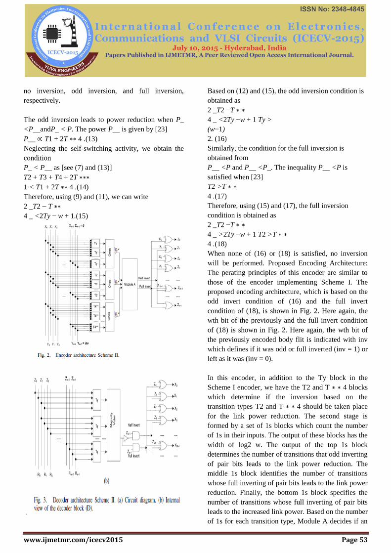
www.ijmetmr.com/icecv2015 Page 53
no inversion, odd inversion, and full inversion,
respectively.
The odd inversion leads to power reduction when P_
<P__andP_ < P. The power P__ is given by [23]
P__ ∝ T1 + 2T ∗∗ 4 .(13)
Neglecting the self-switching activity, we obtain the
condition
P_ < P__ as [see (7) and (13)]
T2 + T3 + T4 + 2T ∗∗∗
1 < T1 + 2T ∗∗ 4 .(14)
Therefore, using (9) and (11), we can write
2 _T2 − T ∗∗
4 _ <2Ty − w + 1.(15)
Based on (12) and (15), the odd inversion condition is
obtained as
2 _T2 −T ∗ ∗
4 _ <2Ty −w + 1 Ty >
(w−1)
2. (16)
Similarly, the condition for the full inversion is
obtained from
P__ <P and P__ <P_. The inequality P__ <P is
satisfied when [23]
T2 >T ∗ ∗
4 .(17)
Therefore, using (15) and (17), the full inversion
condition is obtained as
2 _T2 −T ∗ ∗
4 _ >2Ty −w + 1 T2 >T ∗ ∗
4 .(18)
When none of (16) or (18) is satisfied, no inversion
will be performed. Proposed Encoding Architecture:
The perating principles of this encoder are similar to
those of the encoder implementing Scheme I. The
proposed encoding architecture, which is based on the
odd invert condition of (16) and the full invert
condition of (18), is shown in Fig. 2. Here again, the
wth bit of the previously and the full invert condition
of (18) is shown in Fig. 2. Here again, the wth bit of
the previously encoded body flit is indicated with inv
which defines if it was odd or full inverted (inv = 1) or
left as it was (inv = 0).
In this encoder, in addition to the Ty block in the
Scheme I encoder, we have the T2 and T ∗ ∗ 4 blocks
which determine if the inversion based on the
transition types T2 and T ∗ ∗ 4 should be taken place
for the link power reduction. The second stage is
formed by a set of 1s blocks which count the number
of 1s in their inputs. The output of these blocks has the
width of log2 w. The output of the top 1s block
determines the number of transitions that odd inverting
of pair bits leads to the link power reduction. The
middle 1s block identifies the number of transitions
whose full inverting of pair bits leads to the link power
reduction. Finally, the bottom 1s block specifies the
number of transitions whose full inverting of pair bits
leads to the increased link power. Based on the number
of 1s for each transition type, Module A decides if an
www.ijmetmr.com/icecv2015 Page 54
odd invert or full invert action should be performed for
the power reduction.
For this module, if (16) or (18) is satisfied, the
corresponding output signal will become “1.” In case
no invert action should be taken place, none of the
output is set to “1.” Module A can be implemented
using full-adder and comparator blocks. The circuit
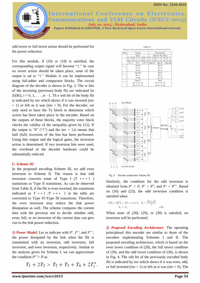
diagram of the decoder is shown in Fig. 3. The w bits
of the incoming (previous) body flit are indicated by
Zi(Ri), i = 0, 1, . . . ,w −1. Th e wth bit of the body flit
is indicated by inv which shows if it was inverted (inv
= 1) or left as it was (inv = 0). For the decoder, we
only need to have the Ty block to determine which
action has been taken place in the encoder. Based on
the outputs of these blocks, the majority voter block
checks the validity of the inequality given by (12). If
the output is “0” (“1”) and the inv = 1,it means that
half (full) inversion of the bits has been performed.
Using this output and the logical gates, the inversion
action is determined. If two inversion bits were used,
the overhead of the decoder hardware could be
substantially reduced.
C. Scheme III
In the proposed encoding Scheme III, we add even
inversion to Scheme II. The reason is that odd
inversion converts some of Type I (T ∗ ∗ ∗ 1 )
transitions to Type II transitions. As can be observed
from Table II, if the flit is even inverted, the transitions
indicated as T ∗ ∗ 1 /T ∗ ∗ ∗ 1 in the table are
converted to Type IV/Type III transitions. Therefore,
the even inversion may reduce the link power
dissipation as well. The scheme compares the current
data with the previous one to decide whether odd,
even, full, or no inversion of the current data can give
rise to the link power reduction.
1) Power Model: Let us indicate with P’, P”, and P”’,
the power dissipated by the link when the flit is
transmitted with no inversion, odd inversion, full
inversion, and even inversion, respectively. Similar to
the analysis given for Scheme I, we can approximate
the condition P”’< P as
Similarly, the condition for the odd inversion is
obtained from P’ < P, P’ < P”, and P’ < P”’. Based
on (16) and (23), the odd inversion condition is
satisfied when
When none of (28), (29), or (30) is satisfied, no
inversion will be performed.
2) Proposed Encoding Architecture: The operating
principlesof this encoder are similar to those of the
encoders implementing Schemes I and II. The
proposed encoding architecture, which is based on the
even invert condition of (28), the full invert condition
of (29), and the odd invert condition of (30), is shown
in Fig. 4. The wth bit of the previously encoded body
flit is indicated by inv which shows if it was even, odd,
or full inverted (inv = 1) or left as it was (inv = 0). The
www.ijmetmr.com/icecv2015 Page 55
first stage of the encoder determines the transition
types while the second stage is formed by a set of 1s
blocks which count the number of ones in their inputs.
In the first stage, we have added the Te blocks which
determine if any of the transition types of T2, T ∗ ∗ 1,
and T ∗ ∗ ∗ 1 is detected for each pair bits of their
inputs. For these transition types, the even invert
action yields link power reduction. Again, we have
four Ones blocks to determine the number of detected
transitions for each Ty, Te, T2, T ∗ ∗ 4, blocks. The
output of the Ones blocks are inputs for Module C.
This module determines if odd, even, full, or no invert
action corresponding to the outputs “10,” “01,” “11,”
or “00,” respectively, should be performed. The
outputs “01,” “11,” and “10” show that whether (28),
(29), and (30), respectively, are satisfied. In this paper,
Module C was designed based on the conditions given
in (28), (29), and (30). Similar to the procedure used to
design the decoder for scheme II, the decoder for
scheme III may be designed.
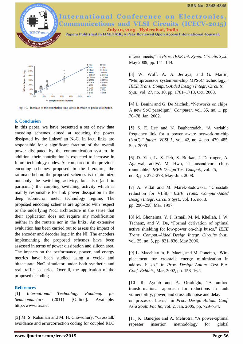
5.Results And Discussion
The proposed data encoding schemes have been
assessed by means of a cycle-accurate NoC simulator
based on Noxim [33]. The power estimation models of
Noxim include NIs, routers, and links [25]. The link
power dissipation was computed using (3) where the
terms T0→1, T1, and T2 were computed based on the
information obtained from the cycle accurate
simulation. The following parameters were used in the
simulations. The NoC was clocked at 700 MHz while
the baseline NI with minimum buffering and
supporting open coreprotocol 2 and advanced high-
performance bus protocols [34]dissipated 5.3 mW. The
average power dissipated by the wormhole-based
router was 5.7 mW. Based on a 65-nm UMC
technology, a total capacitance of 592 fF/mm was
assumed foran inter-router wire. About 80% of this
capacitance was due to the crosstalk. We assumed 2-
mm 32-bit links and a packet size of 16 bytes (eight
flits). Using the detailed simulations, when the flits
traversed the NoC links, the corresponding self and
coupling switching activities were calculated and used
along with the self- and coupling capacitance of 0.237
and0.947 nf, respectively, to calculate the power
(Vdd= 0.9 Vand Fck= 700 MHz).
www.ijmetmr.com/icecv2015 Page 56
6. Conclusion
In this paper, we have presented a set of new data
encoding schemes aimed at reducing the power
dissipated by the linksof an NoC. In fact, links are
responsible for a significant fraction of the overall
power dissipated by the communication system. In
addition, their contribution is expected to increase in
future technology nodes. As compared to the previous
encoding schemes proposed in the literature, the
rationale behind the proposed schemes is to minimize
not only the switching activity, but also (and in
particular) the coupling switching activity which is
mainly responsible for link power dissipation in the
deep submicron meter technology regime. The
proposed encoding schemes are agnostic with respect
to the underlying NoC architecture in the sense that
their application does not require any modification
neither in the routers nor in the links. An extensive
evaluation has been carried out to assess the impact of
the encoder and decoder logic in the NI. The encoders
implementing the proposed schemes have been
assessed in terms of power dissipation and silicon area.
The impacts on the performance, power, and energy
metrics have been studied using a cycle- and
bitaccurate NoC simulator under both synthetic and
real traffic scenarios. Overall, the application of the
proposed encoding
References
[1] International Technology Roadmap for
Semiconductors. (2011) [Online]. Available:
http://www.itrs.net
[2] M. S. Rahaman and M. H. Chowdhury, “Crosstalk
avoidance and errorcorrection coding for coupled RLC
interconnects,” in Proc. IEEE Int. Symp. Circuits Syst.,
May 2009, pp. 141–144.
[3] W. Wolf, A. A. Jerraya, and G. Martin,
“Multiprocessor system-on-chip MPSoC technology,”
IEEE Trans. Comput.-Aided Design Integr. Circuits
Syst., vol. 27, no. 10, pp. 1701–1713, Oct. 2008.
[4] L. Benini and G. De Micheli, “Networks on chips:
A new SoC paradigm,” Computer, vol. 35, no. 1, pp.
70–78, Jan. 2002.
[5] S. E. Lee and N. Bagherzadeh, “A variable
frequency link for a power aware network-on-chip
(NoC),” Integr. VLSI J., vol. 42, no. 4, pp. 479–485,
Sep. 2009.
[6] D. Yeh, L. S. Peh, S. Borkar, J. Darringer, A.
Agarwal, andW. M. Hwu, “Thousand-core chips
roundtable,” IEEE Design Test Comput., vol. 25,
no. 3, pp. 272–278, May–Jun. 2008.
[7] A. Vittal and M. Marek-Sadowska, “Crosstalk
reduction for VLSI,” IEEE Trans. Comput.-Aided
Design Integr. Circuits Syst., vol. 16, no. 3,
pp. 290–298, Mar. 1997.
[8] M. Ghoneima, Y. I. Ismail, M. M. Khellah, J. W.
Tschanz, and V. De, “Formal derivation of optimal
active shielding for low-power on-chip buses,” IEEE
Trans. Comput.-Aided Design Integr. Circuits Syst.,
vol. 25, no. 5, pp. 821–836, May 2006.
[9] L. Macchiarulo, E. Macii, and M. Poncino, “Wire
placement for crosstalk energy minimization in
address buses,” in Proc. Design Autom. Test Eur.
Conf. Exhibit., Mar. 2002, pp. 158–162.
[10] R. Ayoub and A. Orailoglu, “A unified
transformational approach for reductions in fault
vulnerability, power, and crosstalk noise and delay
on processor buses,” in Proc. Design Autom. Conf.
Asia South Pacific, vol. 2. Jan. 2005, pp. 729–734.
[11] K. Banerjee and A. Mehrotra, “A power-optimal
repeater insertion methodology for global
www.ijmetmr.com/icecv2015 Page 57
interconnects in nanometer designs,” IEEE Trans.
Electron Devices, vol. 49, no. 11, pp. 2001–2007, Nov.
2002.
[12] M. R. Stan and W. P. Burleson, “Bus-invert
coding for low-power I/O,” IEEE Trans. Very Large
Scale Integr. (VLSI) Syst., vol. 3, no. 1, pp. 49–58,
Mar. 1995.
[13] S. Ramprasad, N. R. Shanbhag, and I. N. Hajj, “A
coding framework for low-power address and data
busses,” IEEE Trans. Very Large Scale Integr. (VLSI)
Syst., vol. 7, no. 2, pp. 212–221, Jun. 1999.
[14] C. L. Su, C. Y. Tsui, and A. M. Despain, “Saving
power in the control path of embedded processors,”
IEEE Design Test Comput., vol. 11, no. 4, pp. 24–31,
Oct.–Dec. 1994.
[15] L. Benini, G. De Micheli, E. Macii, D. Sciuto, and
C. Silvano, “Asymptotic zero-transition activity
encoding for address busses in low-power
microprocessor-based systems,” in Proc. 7th Great
Lakes Symp. VLSI, Mar. 1997, pp. 77–82.
[16] E. Musoll, T. Lang, and J. Cortadella, “Working-
zone encoding for reducing the energy in
microprocessor address buses,” IEEE Trans. Very
Large Scale Integr. (VLSI) Syst., vol. 6, no. 4, pp. 568–
572, Dec. 1998.
[17] W. Fornaciari, M. Polentarutti, D. Sciuto, and C.
Silvano, “Power optimization of system-level address
buses based on software profiling,” inProc. 8th Int.
Workshop Hardw. Softw.Codesign, May 2000, pp. 29–
33.
[18] L. Benini, G. De Micheli, E. Macii, M. Poncino,
and S. Quer, “Power optimization of core-based
systems by address bus encoding,” IEEE Trans. Very
Large Scale Integr. (VLSI) Syst., vol. 6, no. 4, pp. 554–
562, Dec. 1998.
[19] L. Benini, A. Macii, M. Poncino, and R. Scarsi,
“Architectures and synthesis algorithms for power-
efficient bus interfaces,” IEEE Trans.
Comput.-Aided Design Integr. Circuits Syst., vol. 19,
no. 9, pp. 969–980, Sep. 2000.
[20] G. Ascia, V. Catania, M. Palesi, and A. Parlato,
“Switching activity reduction in embedded systems: A
genetic bus encoding approach,” IEE Proc. Comput.
Digit. Tech., vol. 152, no. 6, pp. 756–764, Nov. 2005.
[21] R. Siegmund, C. Kretzschmar, and D. Muller,
“Adaptive Partial Businvert encoding for power
efficient data transfer over wide system buses,” in
Proc. 13th Symp. Integr. Circuits Syst. Design, Sep.
2000, pp. 371–376.
[22] S. Youngsoo, C. Soo-Ik, and C. Kiyoung, “Partial
bus-invert coding for power optimization of
application-specific systems,” IEEE Trans. Very Large
Scale Integr. (VLSI) Syst., vol. 9, no. 2, pp. 377–383,
Apr. 2001.
[23] M. Palesi, G. Ascia, F. Fazzino, and V. Catania,
“Data encoding schemes in networks on chip,” IEEE
Trans. Comput.-Aided Design Integr. Circuits Syst.,
vol. 30, no. 5, pp. 774–786, May 2011.
[24] C. G. Lyuh and T. Kim, “Low-power bus
encoding with crosstalk delay elimination,” IEE Proc.
Comput. Digit. Tech., vol. 153, no. 2, pp. 93–100, Mar.
2006.
[25] P. P. Pande, H. Zhu, A. Ganguly, and C. Grecu,
“Energy reduction through crosstalk avoidance coding
in NoC paradigm,” in Proc. 9th EUROMICRO Conf.
Digit. Syst. Design Archit. Methods Tools, Sep. 2006,
pp. 689–695.
[26] K. W. Ki, B. Kwang Hyun, N. Shanbhag, C. L.
Liu, and K. M. Sung, “Coupling-driven signal
encoding scheme for low-power interface design,” in
Proc. IEEE/ACM Int. Conf. Comput.-Aided Design,
Nov. 2000, pp. 318–321.
[27] L. Rung-Bin, “Inter-wire coupling reduction
analysis of bus-invert coding,” IEEE Trans. Circuits
Syst. I, Reg. Papers, vol. 55, no. 7, pp. 1911–1920,
Aug. 2008.
www.ijmetmr.com/icecv2015 Page 58
[28] Z. Khan, T. Arslan, and A. T. Erdogan, “Low
power system on chip bus encoding scheme with
crosstalk noise reduction capability,” IEE Proc.
Comput.Digit. Tech., vol. 153, no. 2, pp. 101–108,
Mar. 2006.
[29] Z. Yan, J. Lach, K. Skadron, and M. R. Stan,
“Odd/even bus invert with two-phase transfer for buses
with coupling,” in Proc. Int. Symp. Low Power
Electron. Design, 2002, pp. 80–83.
[30] C. P. Fan and C. H. Fang, “Efficient RC low-
power bus encoding methods for crosstalk reduction,”
Integr. VLSI J., vol. 44, no. 1, pp. 75–86, Jan. 2011.
[31] S. R. Vangal, J. Howard, G. Ruhl, S. Dighe, H.
Wilson, J. Tschanz, W. James, D. Finan, A. P. Singh,
T. Jacob, S. Jain, V. Erraguntla, C. Roberts, Y. V.
Hoskote, N. Y. Borkar, and S. Y. Borkar, “An 80-tile
Sub-100-W TeraFLOPS processor in 65-nm CMOS,”
IEEE J. Solid-State Circuits, vol. 43, no. 1, pp. 29–41,
Jan. 2008.
[32] S. Murali, C. Seiculescu, L. Benini, and G. De
Micheli, “Synthesis of networks on chips for 3D
systems on chips,” in Proc. Asia South Pacific Design
Autom. Conf., Jan. 2009, pp. 242–247.
[33] C. Seiculescu, S. Murali, L. Benini, and G. De
Micheli, “SunFloor 3D: A tool for networks on chip
topology synthesis for 3-D systems on chips,” in Proc.
IEEE Trans. Comput.-Aided Design Integr. Circuits
Syst., vol. 29, no. 12, pp. 1987–2000, Dec. 2010.
[34] S. Murali and G. De Micheli, “Bandwidth-
constrained mapping of cores onto NoC architectures,”
in Proc. Design, Autom. Test Eur. Conf. Exhibit., vol.
2. Feb. 2004, pp. 896–901.
[35] M. Palesi, R. Tornero, J. M. Orduñna, V. Catania,
and D. Panno, “Designing robust routing algorithms
and mapping cores in networks-onchip: A multi-
objective evolutionary-based approach,” J. Univ.
Comput. Sci., vol. 18, no. 7, pp. 937–969, 2012.
Author’s Profiles:
Author-1:
Ms. Panuganti Sandhya receiving her PG degree
specialized in VLSI in Vaagdevi College of
Engineering, Bollikunta, Warangal in the year 2015
and completed her B.Tech from Vaagdevi College of
Engineering and she is interested in the area of VLSI.
Author-2:
Mr. Konda Tirupathi working as Asst. Professor in
Vaagdevi College of Engineering, Bollikunta,
Warangal. He is interested in the area of VLSI.