Embed Size (px)
Citation preview

Protection of accelerator hardware : RF systems
Joint Accelerator School November 11, 2014
SANG-HO KIM
SNS/ORNL
This course will go through some selective topics only will not touch details (90 min. course) RF system layout arcing/discharge mechanism possible damages from high intensity beam discuss about protection Due to large spread of area expertise between students, the lecture materials are prepared accordingly One homework for student credit
0.0
0.5
1.0
1.5
2.0
2.5
3.0
0 500 1000 1500 2000 2500
50eV 1500eV
Electron energy (eV) Se
con
dar
y Em
issi
on
Yie
ld
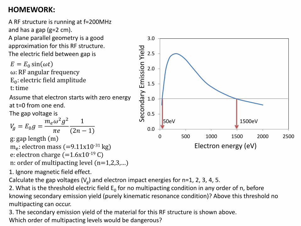
HOMEWORK:
A RF structure is running at f=200MHz and has a gap (g=2 cm). A plane parallel geometry is a good approximation for this RF structure. The electric field between gap is
𝑉𝑔 = 𝐸0𝑔 =𝑚𝑒𝜔2𝑔2
𝜋𝑒
1
(2𝑛 − 1)
g: gap length m me: electron mass (=9.11x10⁻³¹ kg) e: electron charge (=1.6x10⁻¹⁹ C) n: order of multipacting level (n=1,2,3,…)
1. Ignore magnetic field effect. Calculate the gap voltages (Vg) and electron impact energies for n=1, 2, 3, 4, 5. 2. What is the threshold electric field E0 for no multipacting condition in any order of n, before knowing secondary emission yield (purely kinematic resonance condition)? Above this threshold no multipacting can occur.
3. The secondary emission yield of the material for this RF structure is shown above. Which order of multipacting levels would be dangerous?
Assume that electron starts with zero energy at t=0 from one end. The gap voltage is
𝐸 = 𝐸0 sin 𝜔𝑡 ω: RF angular frequency E0: electric field amplitude t: time
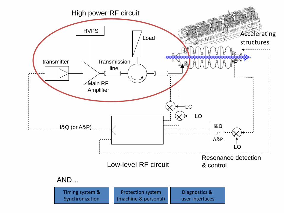
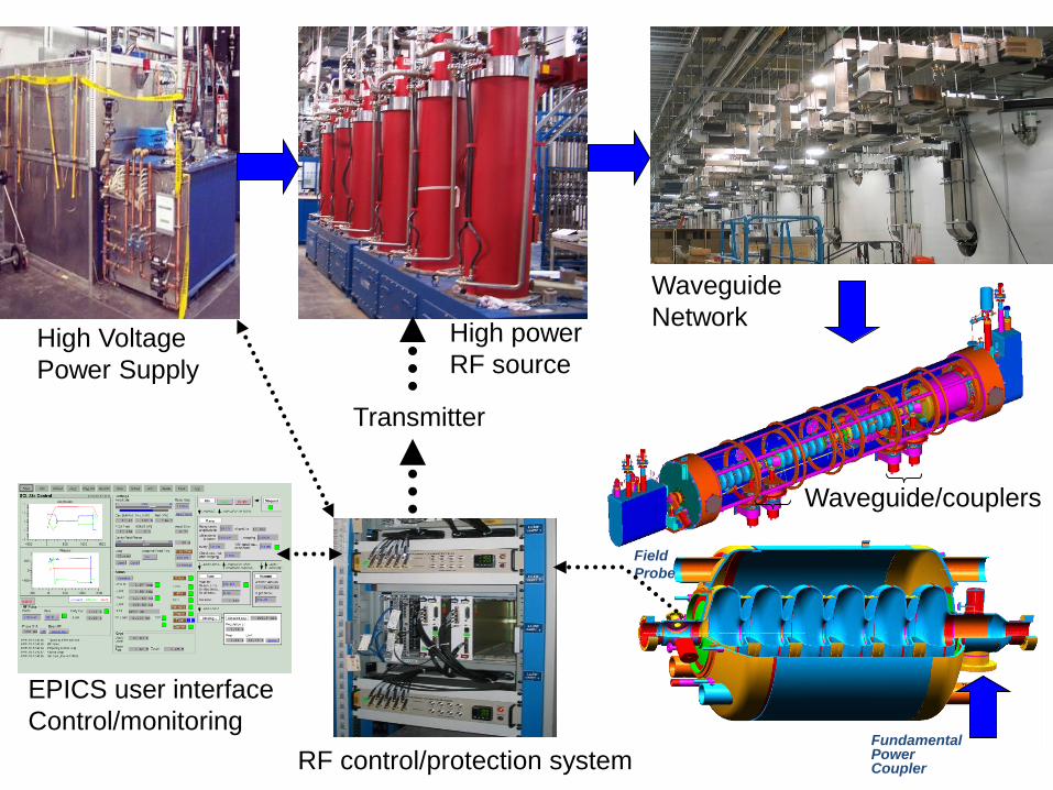
RF system layout
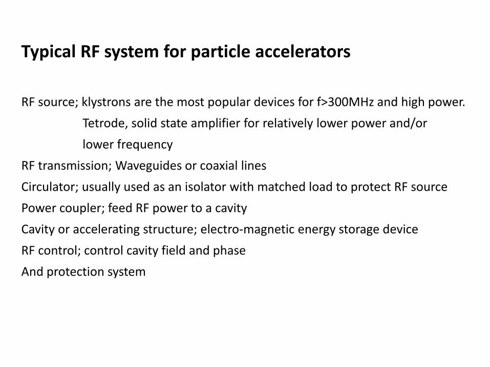
Typical RF system for particle accelerators
RF source; klystrons are the most popular devices for f>300MHz and high power.
Tetrode, solid state amplifier for relatively lower power and/or
lower frequency
RF transmission; Waveguides or coaxial lines
Circulator; usually used as an isolator with matched load to protect RF source
Power coupler; feed RF power to a cavity
Cavity or accelerating structure; electro-magnetic energy storage device
RF control; control cavity field and phase
And protection system
HVPS
High power RF circuit
Low-level RF circuit
Main RF
Amplifier
Transmission
line
LO
LO
LO
I&Q or
A&P
I&Q (or A&P)
Timing system & Synchronization
transmitter
AND…
Protection system (machine & personal)
Diagnostics & user interfaces
Load
Resonance detection
& control
Accelerating structures
Fundamental Power Coupler
Field
Probe
High Voltage
Power Supply
High power
RF source
Waveguide
Network
Waveguide/couplers
RF control/protection system
EPICS user interface
Control/monitoring
Transmitter
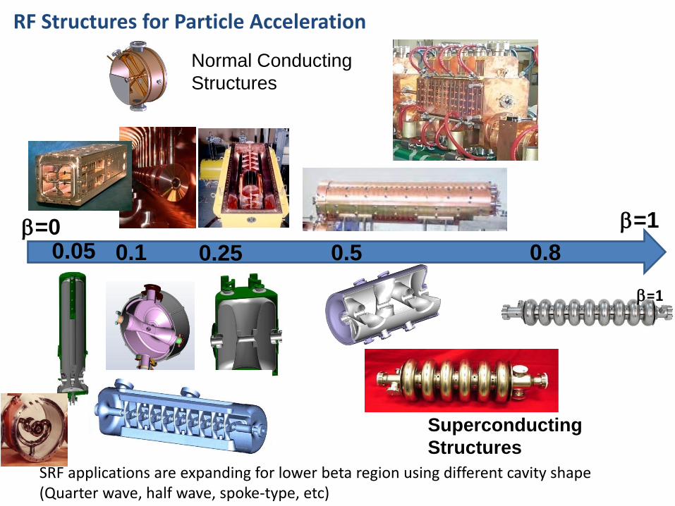
RF Structures for Particle Acceleration
=0 =1
0.05 0.1 0.25 0.5 0.8
Normal Conducting
Structures
Superconducting
Structures
SRF applications are expanding for lower beta region using different cavity shape (Quarter wave, half wave, spoke-type, etc)
=1
What could go wrong regarding machine protection?
Goal: Keep the system in a reliably operable condition preferably forever or till equipment lifetime! (normal large scale machines run about 40-50 years, klystron’s life time 10-15 years, etc.) In general, high voltage, high power RF system and RF structures give the most downtime in operating machines. Equipment/parts damages – would require long and expensive rework/rebuild/replacement (and require large numbers of spares) There are lots of elements that can cause damages and lead to catastrophic failures
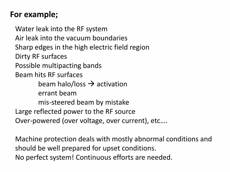
For example;
Water leak into the RF system Air leak into the vacuum boundaries Sharp edges in the high electric field region Dirty RF surfaces Possible multipacting bands Beam hits RF surfaces beam halo/loss activation errant beam mis-steered beam by mistake Large reflected power to the RF source Over-powered (over voltage, over current), etc…. Machine protection deals with mostly abnormal conditions and should be well prepared for upset conditions. No perfect system! Continuous efforts are needed.
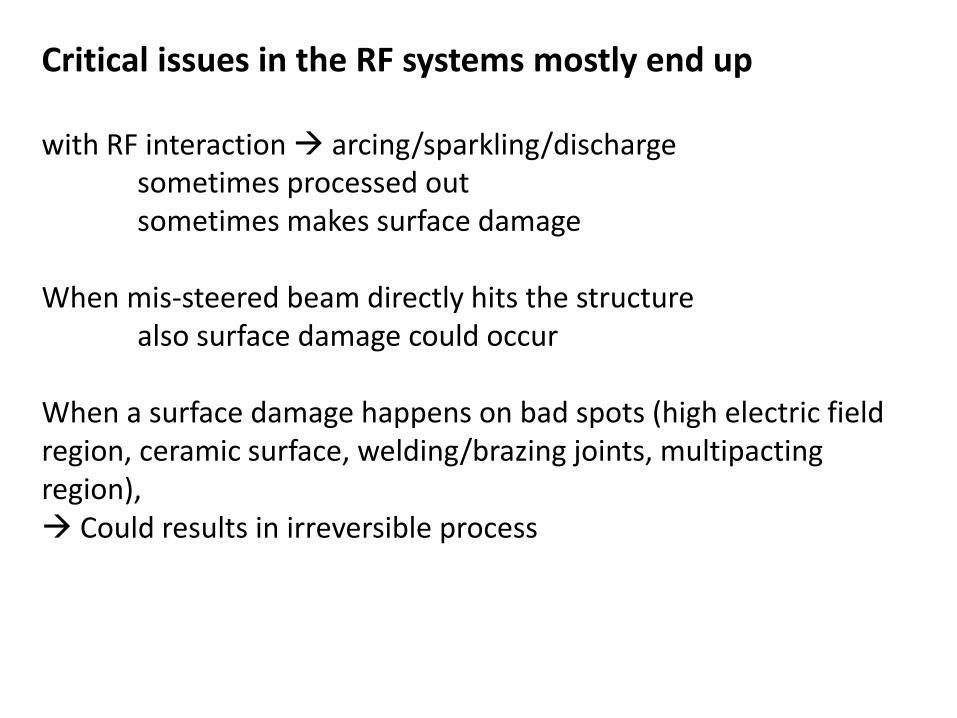
Critical issues in the RF systems mostly end up
with RF interaction arcing/sparkling/discharge sometimes processed out sometimes makes surface damage When mis-steered beam directly hits the structure also surface damage could occur When a surface damage happens on bad spots (high electric field region, ceramic surface, welding/brazing joints, multipacting region), Could results in irreversible process
Discharge mechanism
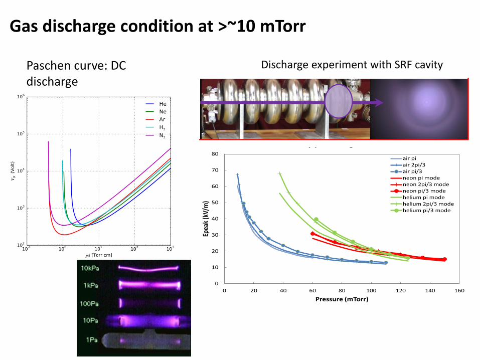
Gas discharge condition at >~10 mTorr
Paschen curve: DC discharge
0
10
20
30
40
50
60
70
80
0 20 40 60 80 100 120 140 160
Epea
k (k
V/m
)
Pressure (mTorr)
Cavity plasma Ignition
air piair 2pi/3air pi/3neon pi modeneon 2pi/3 modeneon pi/3 modehelium pi modehelium 2pi/3 modehelium pi/3 mode
Discharge experiment with SRF cavity
Glows and Arcs
Glow discharge: Cold surfaces or electrodes (thermionic emission and field emission: negligible). Electron emission source: secondary from the surface by ion, radical, photon. Large fraction of electrons: from electron avalanche multiplication in the gas
layers adjacent to the cathode (or surfaces). In DC glow discharge, large potential drop (a few hundred V) near cathode
sputtering of cathode material. (often glow discharge application: sputter deposition or etching)
Arc: Large electron emission from surfaces (by thermionic and/or field emission) in a
small area of the surface can occur. The concentrated current flow can produce a very high temperature very locally. even though majority of surface is cold local dense plasma We are talking about very small dimension small potential can lead a very high
peak electric field. high electron current can be produced without electron multiplication in a gas.
In high vacuum
; electron mean free path >> structure dimension
; no formation of electron avalanches in space as in gas discharge
Breakdown mechanism is not well understood yet
• Particle exchange mechanism
• Clump theory
• Field emission mechanism
DC Vacuum breakdown
Raymond L. Boxman, Handbook of vacuum arc science and technology (1995)
M S. Naidu, V. Kamaraju, High voltage engineering (1995)
Particle exchange theory
Charged particle come out of one electrode under high electric field; statistically always possible
Accelerated and hit another electrode; liberate particles
Oppositely charged particle back to the first electrode
When this process becomes cumulative chain reaction
Usually when applied voltage is > a few hundred kV
Clump theory
When loosely bound particles (clusters) exist on surface
This particles (clusters) get charged under high electric field
Accelerated and hit the other surface vaporization breakdown
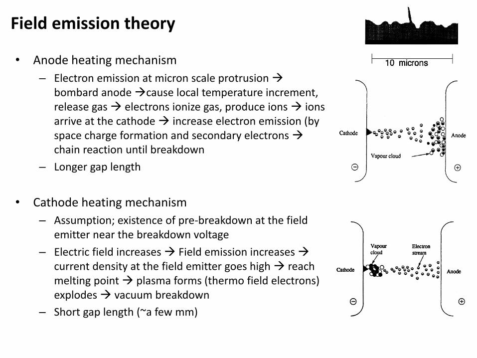
Field emission theory
• Anode heating mechanism
– Electron emission at micron scale protrusion bombard anode cause local temperature increment, release gas electrons ionize gas, produce ions ions arrive at the cathode increase electron emission (by space charge formation and secondary electrons chain reaction until breakdown
– Longer gap length
• Cathode heating mechanism
– Assumption; existence of pre-breakdown at the field emitter near the breakdown voltage
– Electric field increases Field emission increases current density at the field emitter goes high reach melting point plasma forms (thermo field electrons) explodes vacuum breakdown
– Short gap length (~a few mm)
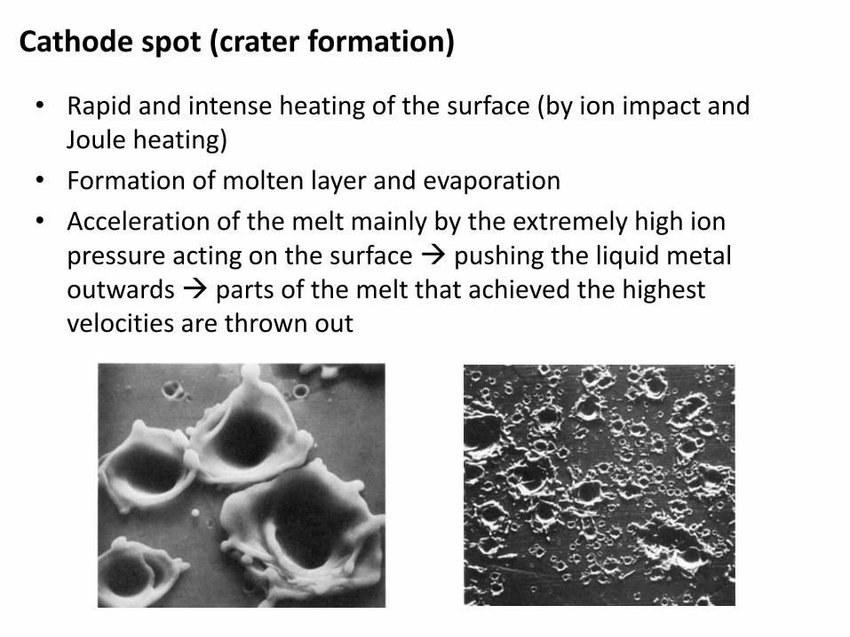
Cathode spot (crater formation)
• Rapid and intense heating of the surface (by ion impact and Joule heating)
• Formation of molten layer and evaporation
• Acceleration of the melt mainly by the extremely high ion pressure acting on the surface pushing the liquid metal outwards parts of the melt that achieved the highest velocities are thrown out
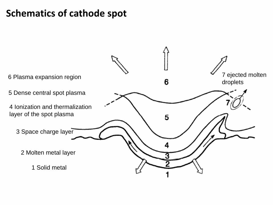
Schematics of cathode spot
1 Solid metal
2 Molten metal layer
3 Space charge layer
4 Ionization and thermalization
layer of the spot plasma
5 Dense central spot plasma
6 Plasma expansion region 7 ejected molten
droplets
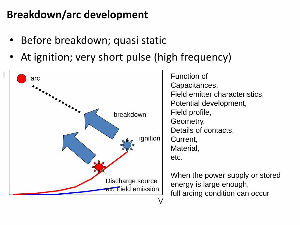
Breakdown/arc development
• Before breakdown; quasi static
• At ignition; very short pulse (high frequency)
Function of
Capacitances,
Field emitter characteristics,
Potential development,
Field profile,
Geometry,
Details of contacts,
Current,
Material,
etc.
When the power supply or stored
energy is large enough,
full arcing condition can occur
I
V
Discharge source
ex. Field emission
ignition
breakdown
arc
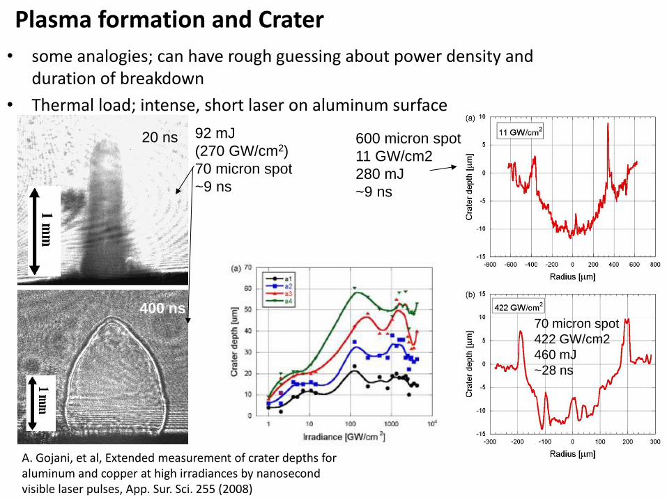
Plasma formation and Crater
• some analogies; can have rough guessing about power density and duration of breakdown
• Thermal load; intense, short laser on aluminum surface
20 ns
400 ns
92 mJ
(270 GW/cm2)
70 micron spot
~9 ns
600 micron spot
11 GW/cm2
280 mJ
~9 ns
70 micron spot
422 GW/cm2
460 mJ
~28 ns
A. Gojani, et al, Extended measurement of crater depths for aluminum and copper at high irradiances by nanosecond visible laser pulses, App. Sur. Sci. 255 (2008)
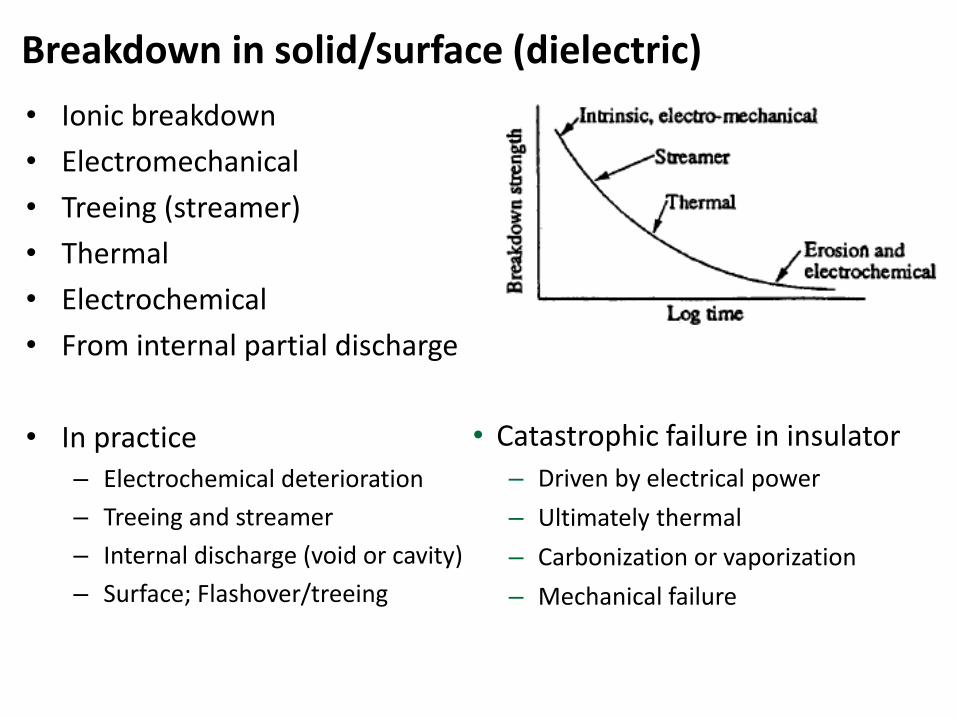
Breakdown in solid/surface (dielectric)
• Ionic breakdown
• Electromechanical
• Treeing (streamer)
• Thermal
• Electrochemical
• From internal partial discharge
• In practice – Electrochemical deterioration
– Treeing and streamer
– Internal discharge (void or cavity)
– Surface; Flashover/treeing
• Catastrophic failure in insulator
– Driven by electrical power
– Ultimately thermal
– Carbonization or vaporization
– Mechanical failure
Dielectric breakdown enhancing factors
• external source for charge buildup
• Non-uniformity
– Provide initiation
– Field concentration
– Non-uniform charge buildup
– void, impurity, inhomogeneity of material, insulator related at contact, junction at the boundary, absorbed gases, wrinkles, contact/boundary material, temperature dependencies, etc.
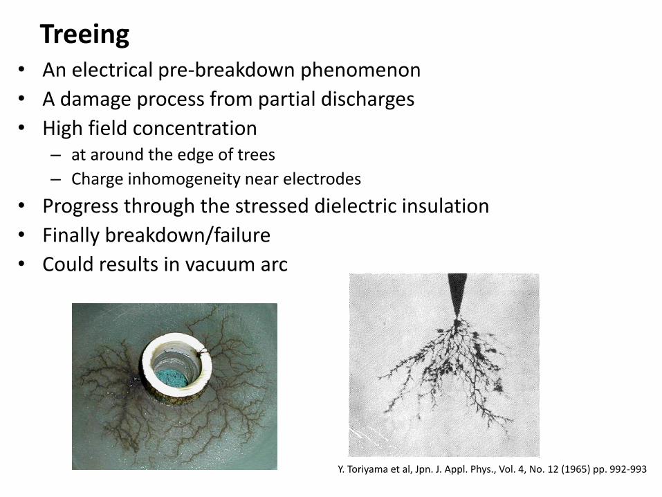
Treeing • An electrical pre-breakdown phenomenon
• A damage process from partial discharges
• High field concentration – at around the edge of trees
– Charge inhomogeneity near electrodes
• Progress through the stressed dielectric insulation
• Finally breakdown/failure
• Could results in vacuum arc
Y. Toriyama et al, Jpn. J. Appl. Phys., Vol. 4, No. 12 (1965) pp. 992-993
Surface Flashover in general
• Field establishment from trapped charge
• Surface charging due to diffusion of trapped charge or from the multiplication of secondary electrons
• Subsequent avalanche of the surface discharge
• Streamer growth of charges
• Breakdown (atoms or clusters)
• Three stage – Initiation
– Development
– Final
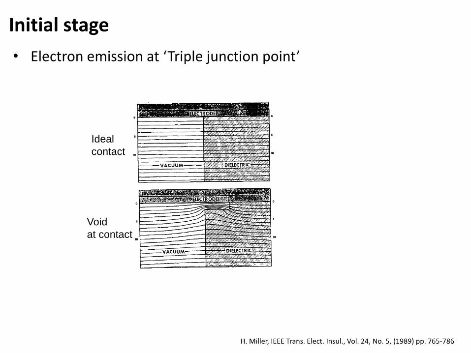
Initial stage
• Electron emission at ‘Triple junction point’
Ideal
contact
Void
at contact
H. Miller, IEEE Trans. Elect. Insul., Vol. 24, No. 5, (1989) pp. 765-786
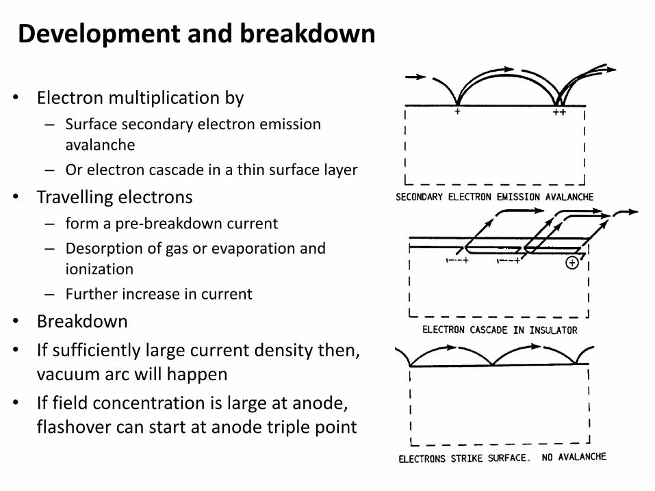
Development and breakdown
• Electron multiplication by
– Surface secondary electron emission avalanche
– Or electron cascade in a thin surface layer
• Travelling electrons
– form a pre-breakdown current
– Desorption of gas or evaporation and ionization
– Further increase in current
• Breakdown
• If sufficiently large current density then, vacuum arc will happen
• If field concentration is large at anode, flashover can start at anode triple point
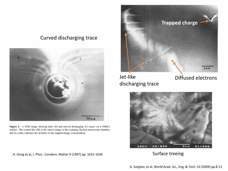
Surface treeing
Jet-like discharging trace
Diffused electrons
Trapped charge
Curved discharging trace
H. Gong et al, J. Phys.: Condens. Matter 9 (1997) pp. 1631-1636
A. Sutjipto, et al, World Acad. Sci., Eng, & Tech. 53 (2009) pp.8-11
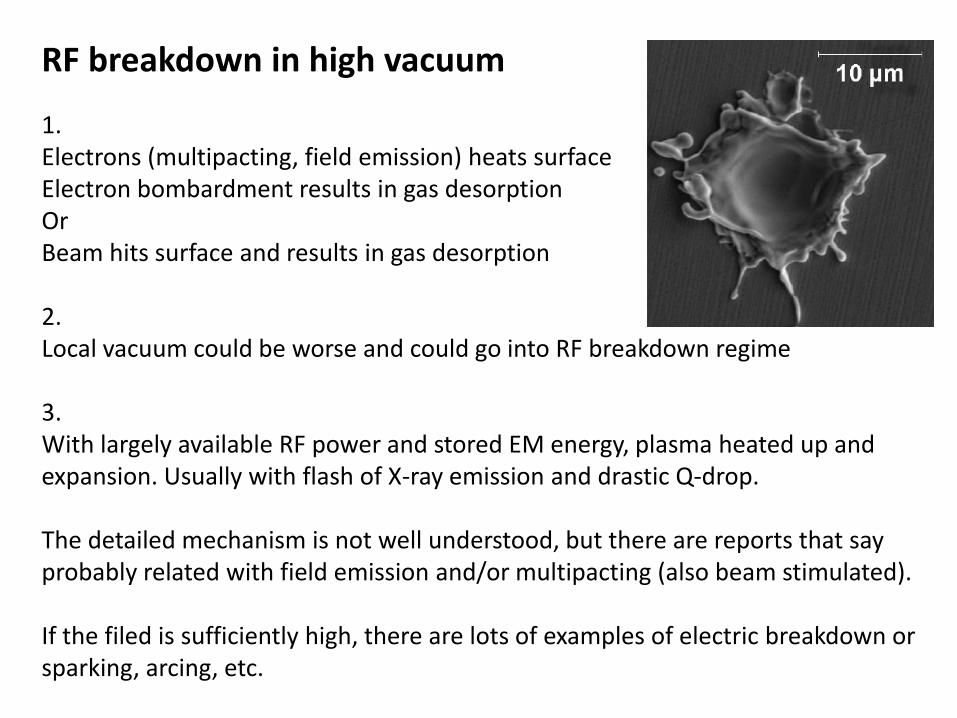
RF breakdown in high vacuum
1. Electrons (multipacting, field emission) heats surface Electron bombardment results in gas desorption Or Beam hits surface and results in gas desorption 2. Local vacuum could be worse and could go into RF breakdown regime 3. With largely available RF power and stored EM energy, plasma heated up and expansion. Usually with flash of X-ray emission and drastic Q-drop. The detailed mechanism is not well understood, but there are reports that say probably related with field emission and/or multipacting (also beam stimulated). If the filed is sufficiently high, there are lots of examples of electric breakdown or sparking, arcing, etc.
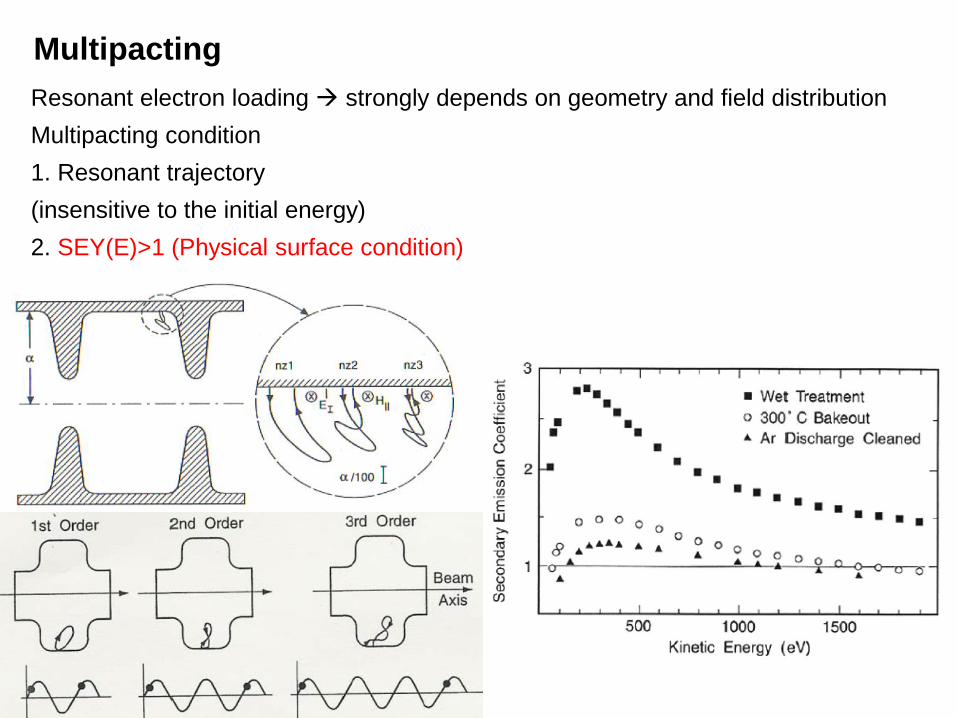
Resonant electron loading strongly depends on geometry and field distribution
Multipacting condition
1. Resonant trajectory
(insensitive to the initial energy)
2. SEY(E)>1 (Physical surface condition)
Multipacting
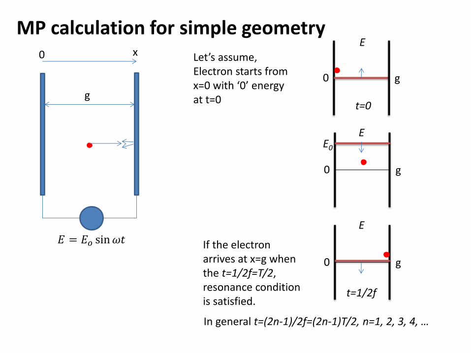
MP calculation for simple geometry
g
𝐸 = 𝐸𝑜 sin 𝜔𝑡
Let’s assume, Electron starts from x=0 with ‘0’ energy at t=0
x 0
t=0
0 g
E
0 g
E E0
t=1/2f
0 g
E
If the electron arrives at x=g when the t=1/2f=T/2, resonance condition is satisfied.
In general t=(2n-1)/2f=(2n-1)T/2, n=1, 2, 3, 4, …
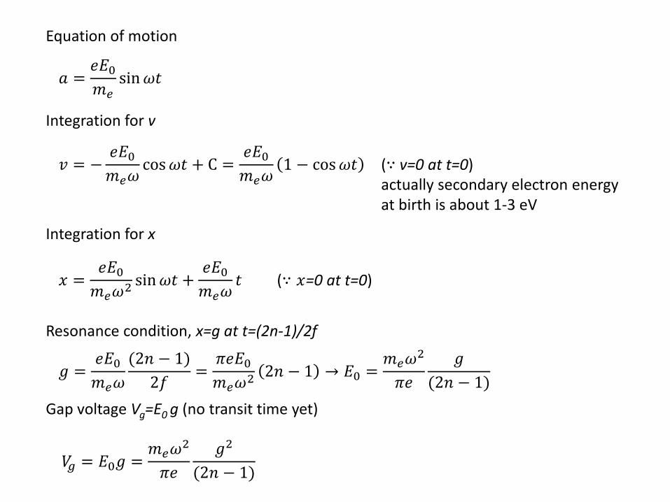
Equation of motion
𝑎 =𝑒𝐸0
𝑚𝑒sin 𝜔𝑡
Integration for v
𝑣 = −𝑒𝐸0
𝑚𝑒𝜔cos 𝜔𝑡 + C =
𝑒𝐸0
𝑚𝑒𝜔1 − cos 𝜔𝑡 (∵ v=0 at t=0)
actually secondary electron energy at birth is about 1-3 eV
Integration for x
𝑥 =𝑒𝐸0
𝑚𝑒𝜔2 sin 𝜔𝑡 +𝑒𝐸0
𝑚𝑒𝜔𝑡 (∵ 𝑥=0 at t=0)
Resonance condition, x=g at t=(2n-1)/2f
𝑔 =𝑒𝐸0
𝑚𝑒𝜔
(2𝑛 − 1)
2𝑓=
𝜋𝑒𝐸0
𝑚𝑒𝜔2 2𝑛 − 1 → 𝐸0 =𝑚𝑒𝜔2
𝜋𝑒
𝑔
(2𝑛 − 1)
Gap voltage Vg=E0 g (no transit time yet)
𝑉𝑔 = 𝐸0𝑔 =𝑚𝑒𝜔2
𝜋𝑒
𝑔2
(2𝑛 − 1)
0 g
E0
𝐸 = 𝐸𝑜 sin 𝜔𝑡
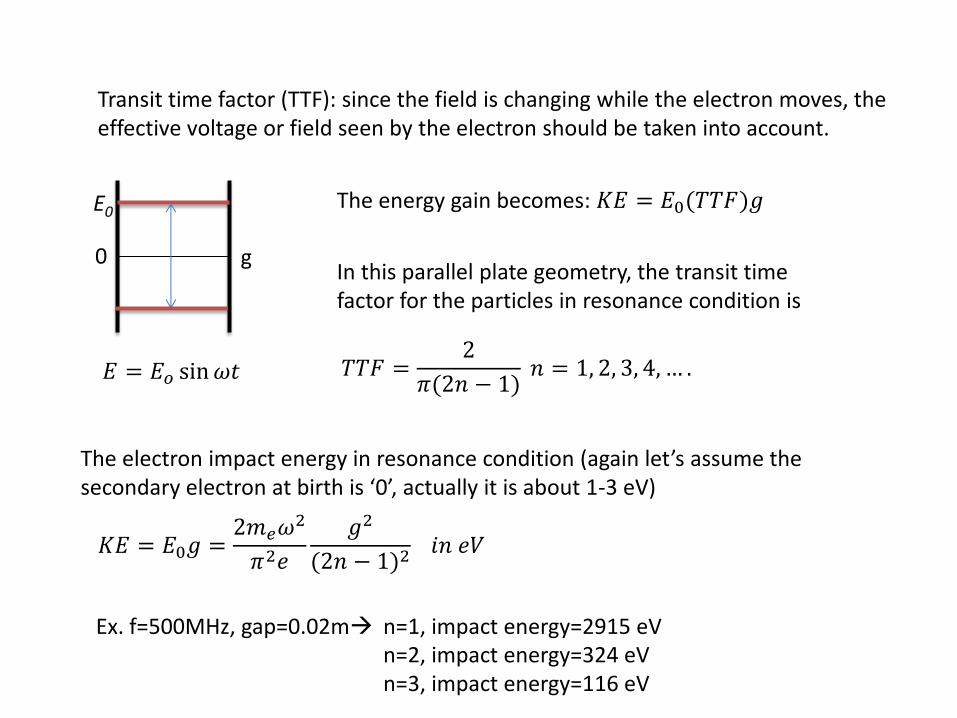
Transit time factor (TTF): since the field is changing while the electron moves, the effective voltage or field seen by the electron should be taken into account.
In this parallel plate geometry, the transit time factor for the particles in resonance condition is
The energy gain becomes: 𝐾𝐸 = 𝐸0(𝑇𝑇𝐹)𝑔
𝑇𝑇𝐹 =2
𝜋(2𝑛 − 1) 𝑛 = 1, 2, 3, 4, … .
The electron impact energy in resonance condition (again let’s assume the secondary electron at birth is ‘0’, actually it is about 1-3 eV)
𝐾𝐸 = 𝐸0𝑔 =2𝑚𝑒𝜔2
𝜋2𝑒
𝑔2
(2𝑛 − 1)2 𝑖𝑛 𝑒𝑉
Ex. f=500MHz, gap=0.02m n=1, impact energy=2915 eV n=2, impact energy=324 eV n=3, impact energy=116 eV
Multipacting in general MP is mostly at low electric field side. during ramp-up beam pipe (stray field region) window, iris, couplers equator sides of cavity , etc How to avoid: Careful analysis during design stage & simplify the design (avoid resonances) Reduce Secondary Emission Yield Keep the surface clean (no contaminant, gas, particulates..) RF conditioning reduces Baking, discharge cleaning, Surface coating (Ti, TiN) DC biasing *Detuning Slight change of VSWR: sometimes helps when MP happens in the
transmission line (waveguide, window, coupler, etc.) *Over-coupling (lower time constant) to pass MP region quickly especially in pulse machine *very limited range of control
Cavity D 12 MV/m
Camera exposure; 30 ms Cavity A 9.3MV/m
Camera exposure; 30 ms
Phosphor screen images
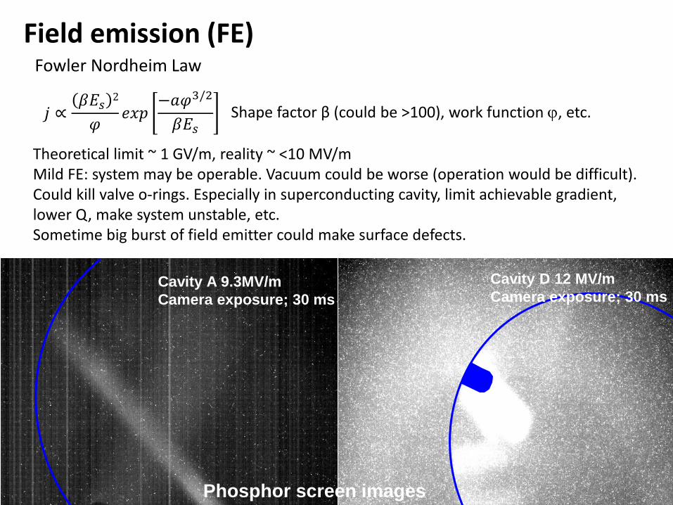
Fowler Nordheim Law
Shape factor β (could be >100), work function , etc. 𝑗 ∝𝛽𝐸𝑠
2
𝜑𝑒𝑥𝑝
−𝑎𝜑3/2
𝛽𝐸𝑠
Field emission (FE)
Theoretical limit ~ 1 GV/m, reality ~ <10 MV/m Mild FE: system may be operable. Vacuum could be worse (operation would be difficult). Could kill valve o-rings. Especially in superconducting cavity, limit achievable gradient, lower Q, make system unstable, etc. Sometime big burst of field emitter could make surface defects.
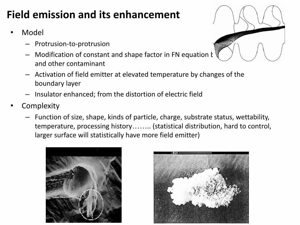
Field emission and its enhancement
• Model
– Protrusion-to-protrusion
– Modification of constant and shape factor in FN equation by absorbed gases and other contaminant
– Activation of field emitter at elevated temperature by changes of the boundary layer
– Insulator enhanced; from the distortion of electric field
• Complexity
– Function of size, shape, kinds of particle, charge, substrate status, wettability, temperature, processing history…….. (statistical distribution, hard to control, larger surface will statistically have more field emitter)
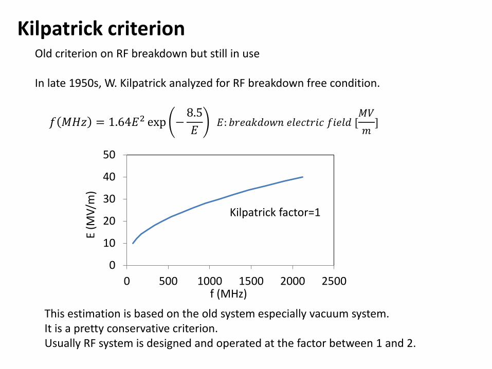
Kilpatrick criterion Old criterion on RF breakdown but still in use In late 1950s, W. Kilpatrick analyzed for RF breakdown free condition.
𝑓 𝑀𝐻𝑧 = 1.64𝐸2 exp −8.5
𝐸 𝐸: 𝑏𝑟𝑒𝑎𝑘𝑑𝑜𝑤𝑛 𝑒𝑙𝑒𝑐𝑡𝑟𝑖𝑐 𝑓𝑖𝑒𝑙𝑑 [
𝑀𝑉
𝑚]
0
10
20
30
40
50
0 500 1000 1500 2000 2500f (MHz)
E (M
V/m
)
This estimation is based on the old system especially vacuum system. It is a pretty conservative criterion. Usually RF system is designed and operated at the factor between 1 and 2.
Kilpatrick factor=1
Vacuum
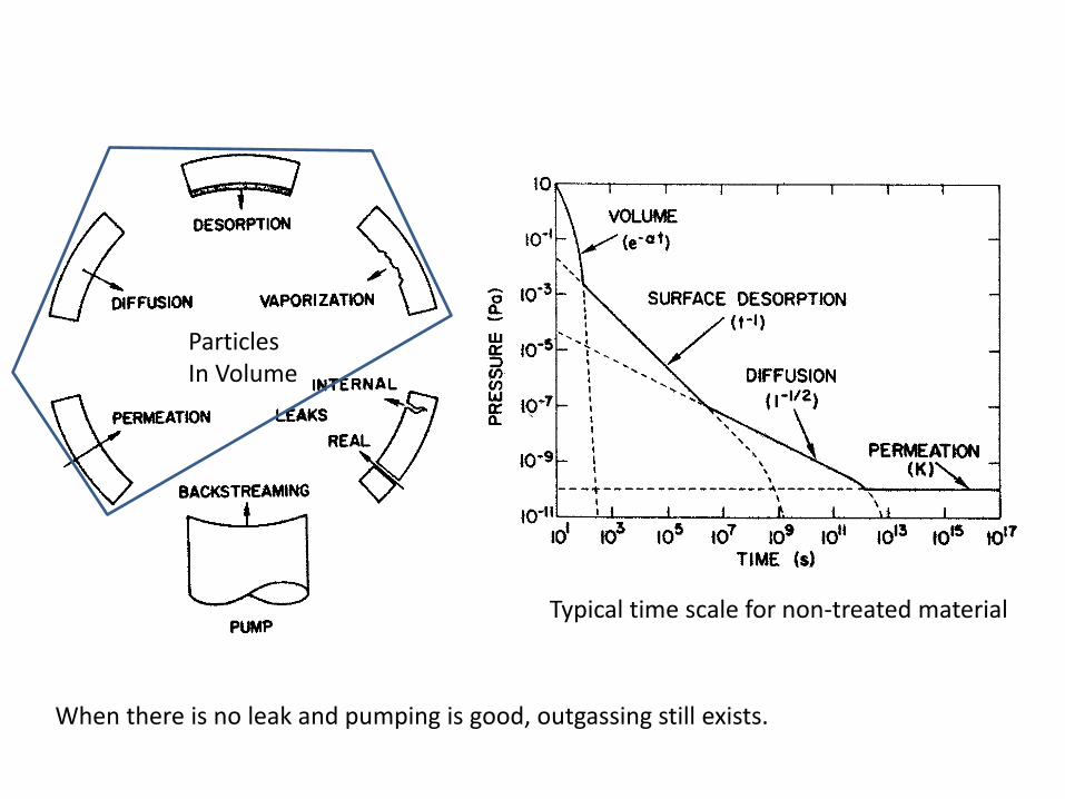
When there is no leak and pumping is good, outgassing still exists.
Typical time scale for non-treated material
Particles In Volume
Outgassing
1. Desorption: gas release from the surface. Final state of all outgassing mechanism. Bonding mechanisms can be either physical or chemical. In general chemical bonding is stronger. Desorption rate increases with temperature. Desorption is accelerated by photons, electrons and ion bombardment. 2. Vaporization: phase transition of material to the gas. Materials with higher vapor pressure can evaporate in vacuum and/or at elevated temperature. 3. Diffusion: dissolved gas in the bulk material moves to the vacuum surface. Hydrogen have high mobility in the bulk material. 4. Permeation: absorbed gas from outside diffuses through the bulk material and then desorbed from the vacuum surface.
Polishing: reduce the effective surface area and the adsorption capacity Heating: baking or firing
150-300C baking is very helpful to get rid of water but not enough for hydrogen. Any metal is a large reservoir of hydrogen. During the heat treatment CO and CO2 are often emitted in addition to hydrogen. Firing temperature: 500 C for OF Copper, 1000 C for Stainless Steel
Gas discharge cleaning Photon or electron bombardment/showering Coating
Reducing Outgassing
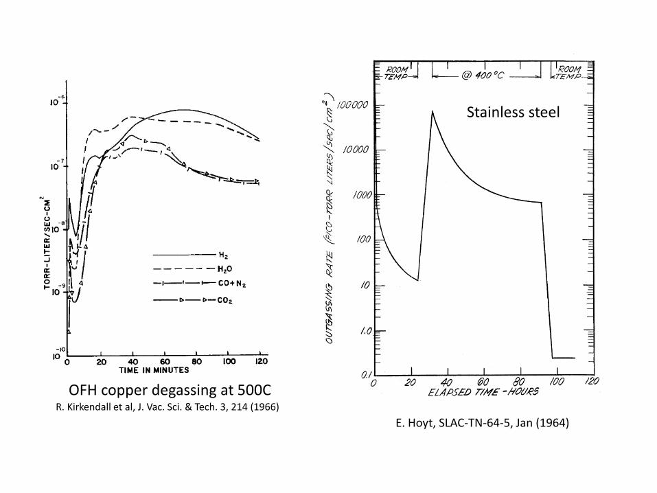
OFH copper degassing at 500C R. Kirkendall et al, J. Vac. Sci. & Tech. 3, 214 (1966)
E. Hoyt, SLAC-TN-64-5, Jan (1964)
Stainless steel
Beam related issues
0.001
0.01
0.1
1
10
100
1000
0.001 0.01 0.1 1 10 100 1000
Ave
rage
Be
am C
urr
en
t (m
A)
Beam Energy (GeV)
Existing (LP) Planned (LP)
Existing (SP) Planned (SP)IPHI LEDA
EFIT
ADS
IFMIF
PSI FRIB RISP
PEFP
SPIRAL-2
ISIS
PSR
TRIUMF
SNS
JPARC RCS
CSNS
MMF
LANSCE
NF/MC Prj-X
Prj-X MR
NUMI
JPARC MR
AGS
CNGS
NOVA
SPL
ESS MYRHHA
SARAF-2
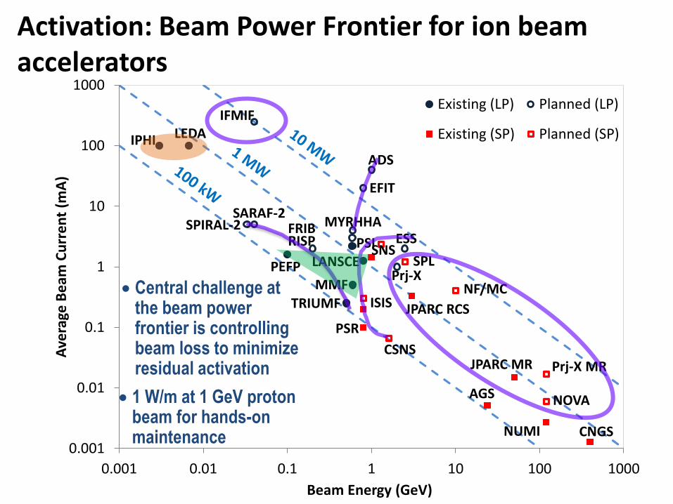
Activation: Beam Power Frontier for ion beam accelerators
Central challenge at the beam power frontier is controlling beam loss to minimize residual activation
1 W/m at 1 GeV proton beam for hands-on maintenance
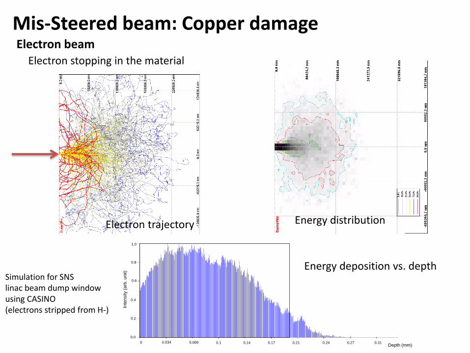
Mis-Steered beam: Copper damage
Electron stopping in the material
Simulation for SNS linac beam dump window using CASINO (electrons stripped from H-)
Electron trajectory Energy distribution
0 0.034 0.069 0.1 0.14 0.17 0.21 0.24 0.27 0.31
1.0
0.8
0.6
0.4
0.2
0.0
Inte
nsity (
arb
. unit)
Depth (mm)
Energy deposition vs. depth
Electron beam
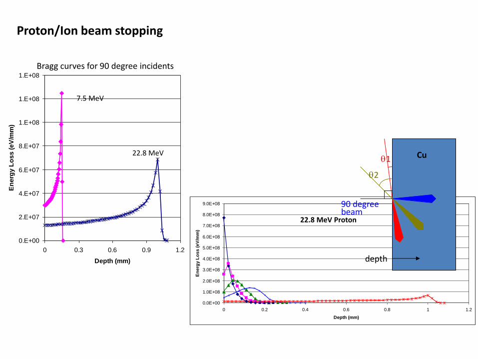
Proton/Ion beam stopping
0.E+00
2.E+07
4.E+07
6.E+07
8.E+07
1.E+08
1.E+08
1.E+08
0 0.3 0.6 0.9 1.2
Depth (mm)
En
erg
y L
os
s (
eV
/mm
)
7.5 MeV
22.8 MeV
Bragg curves for 90 degree incidents
0.0E+00
1.0E+08
2.0E+08
3.0E+08
4.0E+08
5.0E+08
6.0E+08
7.0E+08
8.0E+08
9.0E+08
0 0.2 0.4 0.6 0.8 1 1.2
Depth (mm)
En
erg
y L
os
s (
eV
/mm
)
depth
1
2
90 degree beam
Cu
22.8 MeV Proton
18
0 m
m
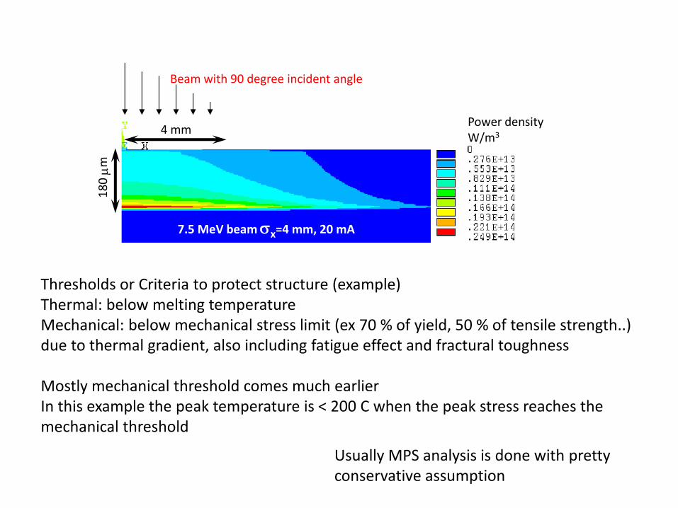
4 mm
7.5 MeV beam sx=4 mm, 20 mA
Beam with 90 degree incident angle
Power density W/m3
Thresholds or Criteria to protect structure (example) Thermal: below melting temperature Mechanical: below mechanical stress limit (ex 70 % of yield, 50 % of tensile strength..) due to thermal gradient, also including fatigue effect and fractural toughness Mostly mechanical threshold comes much earlier In this example the peak temperature is < 200 C when the peak stress reaches the mechanical threshold
Usually MPS analysis is done with pretty conservative assumption
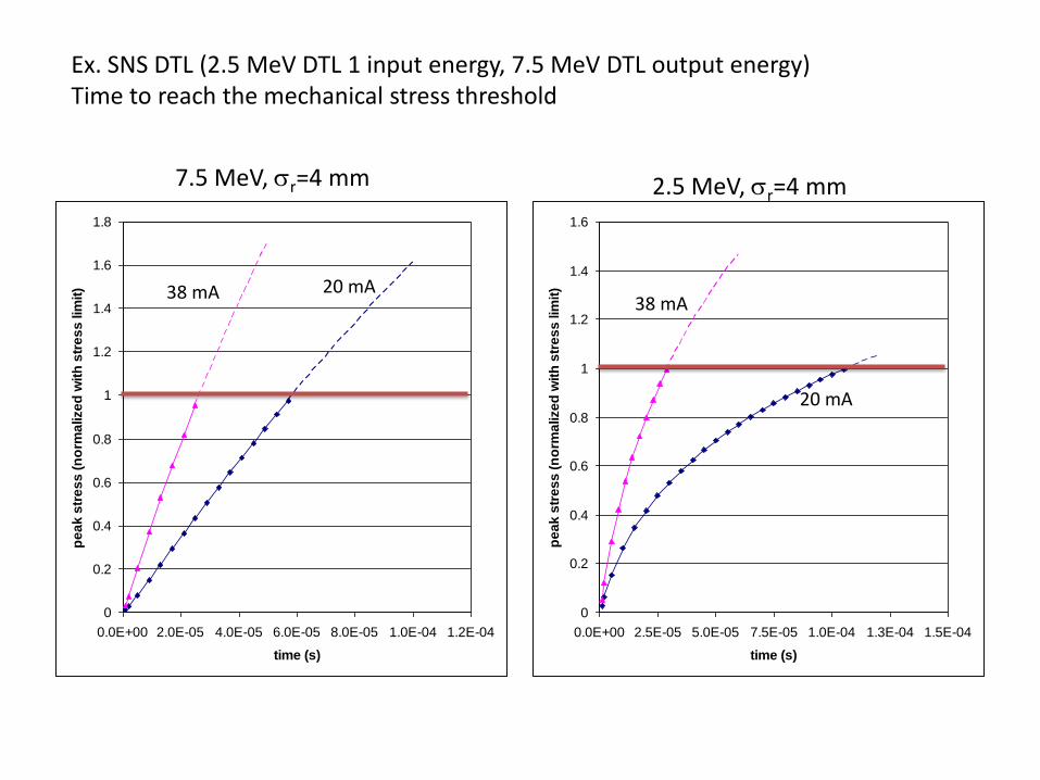
0
0.2
0.4
0.6
0.8
1
1.2
1.4
1.6
1.8
0.0E+00 2.0E-05 4.0E-05 6.0E-05 8.0E-05 1.0E-04 1.2E-04
time (s)
pe
ak
str
es
s (
no
rma
lize
d w
ith
str
es
s lim
it)
0
0.2
0.4
0.6
0.8
1
1.2
1.4
1.6
0.0E+00 2.5E-05 5.0E-05 7.5E-05 1.0E-04 1.3E-04 1.5E-04
time (s)
pe
ak
str
es
s (
no
rma
lize
d w
ith
str
es
s lim
it)38 mA
38 mA 20 mA
20 mA
7.5 MeV, sr=4 mm 2.5 MeV, sr=4 mm
Ex. SNS DTL (2.5 MeV DTL 1 input energy, 7.5 MeV DTL output energy) Time to reach the mechanical stress threshold
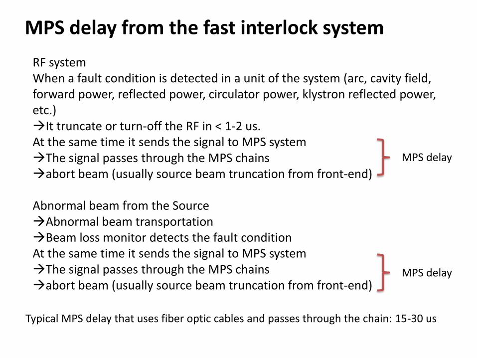
RF system When a fault condition is detected in a unit of the system (arc, cavity field, forward power, reflected power, circulator power, klystron reflected power, etc.) It truncate or turn-off the RF in < 1-2 us. At the same time it sends the signal to MPS system The signal passes through the MPS chains abort beam (usually source beam truncation from front-end) Abnormal beam from the Source Abnormal beam transportation Beam loss monitor detects the fault condition At the same time it sends the signal to MPS system The signal passes through the MPS chains abort beam (usually source beam truncation from front-end)
MPS delay from the fast interlock system
MPS delay
MPS delay
Typical MPS delay that uses fiber optic cables and passes through the chain: 15-30 us
Errant beam
off-energy beam generated anywhere in the accelerator and transported to the downstream in a fault condition
Since the errant beam is off-energy beam, it is mostly lost while transported through the linac, which results in beam trips caused by excessive beam loss.
Errant beam hits cavity surface: desorbs gas or particulates and there’s a non-zero chance for creating an environment for arcing/discharge Dedicated MPS line for the fast interlock system could reduce the MPS delay down to 5-6 us.
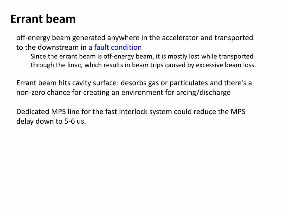
Normal ion source pulse
~ 33 mA
Ion source/LEBT is one cause of errant beams
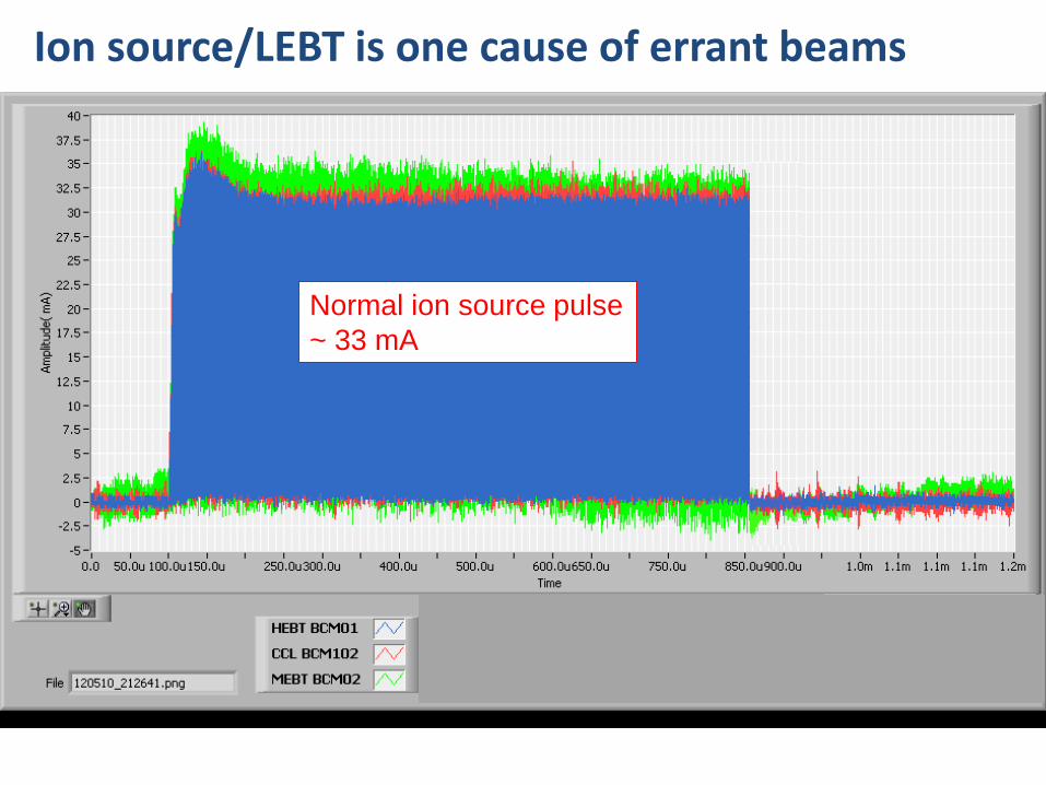
Low current pulse causes
beam loss in SCL
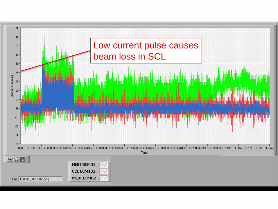
Normal Abnormal
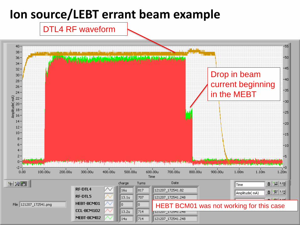
Ion source/LEBT errant beam example
Drop in beam
current beginning
in the MEBT
HEBT BCM01 was not working for this case
DTL4 RF waveform
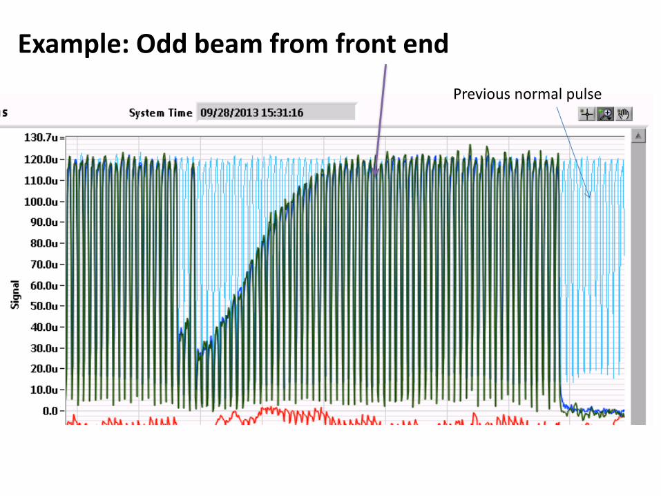
Example: Odd beam from front end
Previous normal pulse
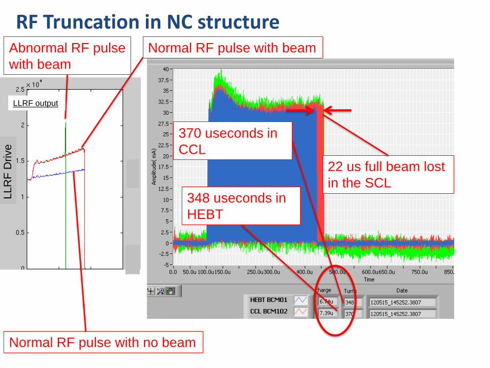
Abnormal RF pulse
with beam
Normal RF pulse with beam
Normal RF pulse with no beam
LLRF output
370 useconds in
CCL
348 useconds in
HEBT
LLR
F D
rive
22 us full beam lost
in the SCL
RF Truncation in NC structure
CCL SRF, =0.61 SRF, =0.81 RFQ
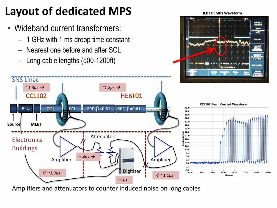
Layout of dedicated MPS
• Wideband current transformers:
– 1 GHz with 1 ms droop time constant
– Nearest one before and after SCL
– Long cable lengths (500-1200ft)
Source MEBT
Amplifier
DTL
Amplifier
Attenuators
Digitizer
SNS Linac
HEBT BCM01 Waveform
Amplifiers and attenuators to counter induced noise on long cables
~1.1µs
~.4µs
~1µs
Electronics Buildings
~1.2µs
~1.3µs
~1.3µs
Understanding of the system is the most important aspect for the safe operation and equipment protection
• Let’s take an example with klystron for machine protection point of view. – how they are designed or fabricated
– Klystron is a high power rf source where many accelerator related components are in place such as electron gun, beam acceleration, RF coupling, beam bunching, maintain high vacuum, DC high voltage, beam dump, RF window, cooling, beam focusing, etc.
• And then discuss about how to protect it.
• Since there are many analogies, this example will help expanding the idea for other equipment.
Klystron
Klystron
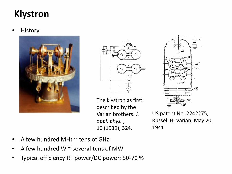
• History
US patent No. 2242275, Russell H. Varian, May 20, 1941
The klystron as first described by the Varian brothers. J. appl. phys. , 10 (1939), 324.
• A few hundred MHz ~ tens of GHz
• A few hundred W ~ several tens of MW
• Typical efficiency RF power/DC power: 50-70 %
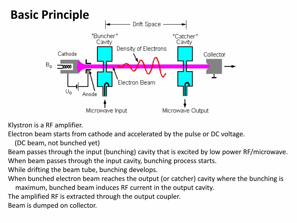
Klystron is a RF amplifier. Electron beam starts from cathode and accelerated by the pulse or DC voltage. (DC beam, not bunched yet) Beam passes through the input (bunching) cavity that is excited by low power RF/microwave. When beam passes through the input cavity, bunching process starts. While drifting the beam tube, bunching develops. When bunched electron beam reaches the output (or catcher) cavity where the bunching is
maximum, bunched beam induces RF current in the output cavity. The amplified RF is extracted through the output coupler. Beam is dumped on collector.
Basic Principle
High voltage 400 kV (ex. S-band 80 MW tube) 130 kV (ex. 700-800 MHz, 5 MW tube) DC Arcing/discharge
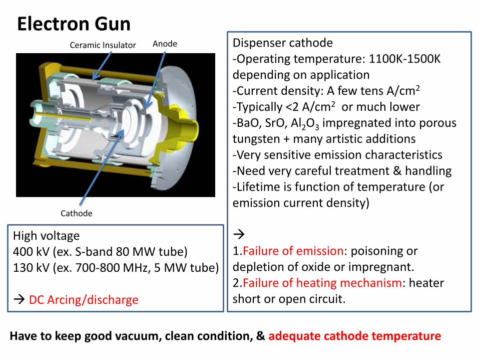
Electron Gun
Cathode
Anode Ceramic Insulator Dispenser cathode -Operating temperature: 1100K-1500K depending on application -Current density: A few tens A/cm2
-Typically <2 A/cm2 or much lower -BaO, SrO, Al2O3 impregnated into porous tungsten + many artistic additions -Very sensitive emission characteristics -Need very careful treatment & handling -Lifetime is function of temperature (or emission current density) 1.Failure of emission: poisoning or depletion of oxide or impregnant. 2.Failure of heating mechanism: heater short or open circuit.
Have to keep good vacuum, clean condition, & adequate cathode temperature
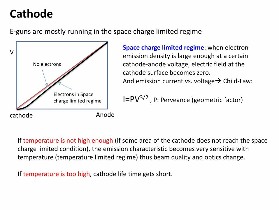
Cathode
E-guns are mostly running in the space charge limited regime
V
cathode Anode
Space charge limited regime: when electron emission density is large enough at a certain cathode-anode voltage, electric field at the cathode surface becomes zero. And emission current vs. voltage Child-Law:
I=PV3/2 , P: Perveance (geometric factor)
No electrons
Electrons in Space charge limited regime
If temperature is not high enough (if some area of the cathode does not reach the space charge limited condition), the emission characteristic becomes very sensitive with temperature (temperature limited regime) thus beam quality and optics change. If temperature is too high, cathode life time gets short.
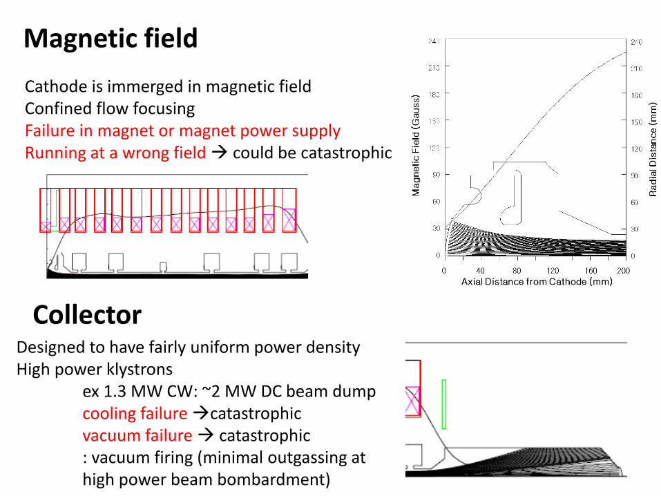
Magnetic field
Cathode is immerged in magnetic field Confined flow focusing Failure in magnet or magnet power supply Running at a wrong field could be catastrophic
Collector Designed to have fairly uniform power density High power klystrons ex 1.3 MW CW: ~2 MW DC beam dump cooling failure catastrophic vacuum failure catastrophic : vacuum firing (minimal outgassing at
high power beam bombardment)
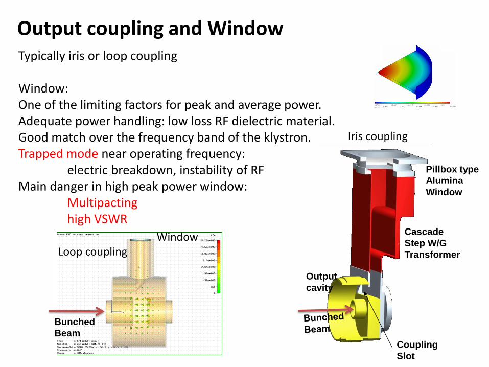
Output coupling and Window Typically iris or loop coupling Window: One of the limiting factors for peak and average power. Adequate power handling: low loss RF dielectric material. Good match over the frequency band of the klystron. Trapped mode near operating frequency: electric breakdown, instability of RF Main danger in high peak power window: Multipacting high VSWR
Output
cavity
Coupling
Slot
Cascade
Step W/G
Transformer
Pillbox type
Alumina
Window
Iris coupling
Loop coupling Window
Bunched
Beam
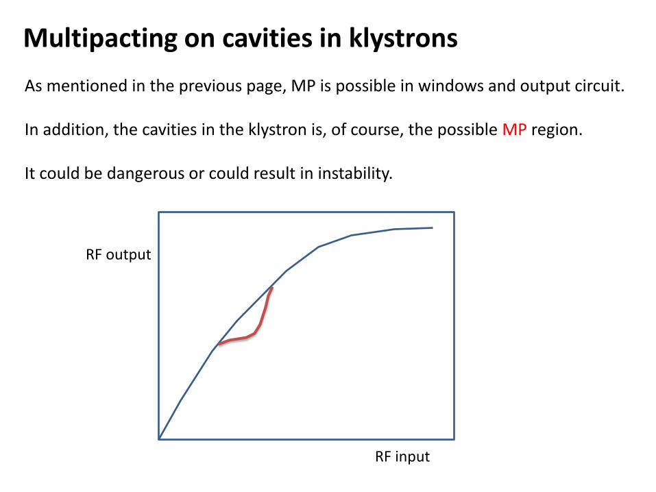
Multipacting on cavities in klystrons
As mentioned in the previous page, MP is possible in windows and output circuit. In addition, the cavities in the klystron is, of course, the possible MP region. It could be dangerous or could result in instability.
RF input
RF output
Couplers
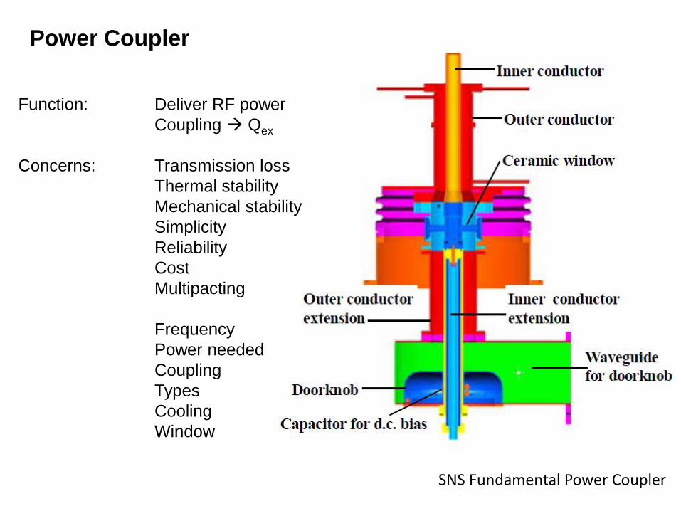
Power Coupler
Function: Deliver RF power
Coupling Qex
Concerns: Transmission loss
Thermal stability
Mechanical stability
Simplicity
Reliability
Cost
Multipacting
Frequency
Power needed
Coupling
Types
Cooling
Window
SNS Fundamental Power Coupler
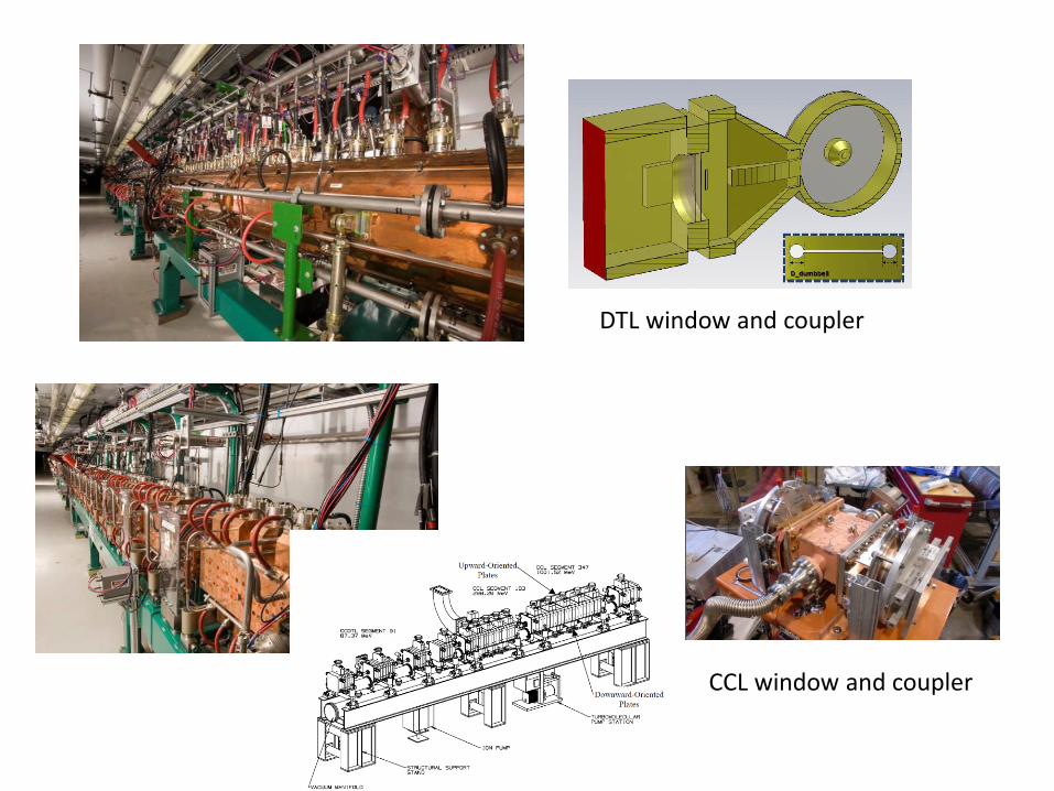
DTL window and coupler
CCL window and coupler
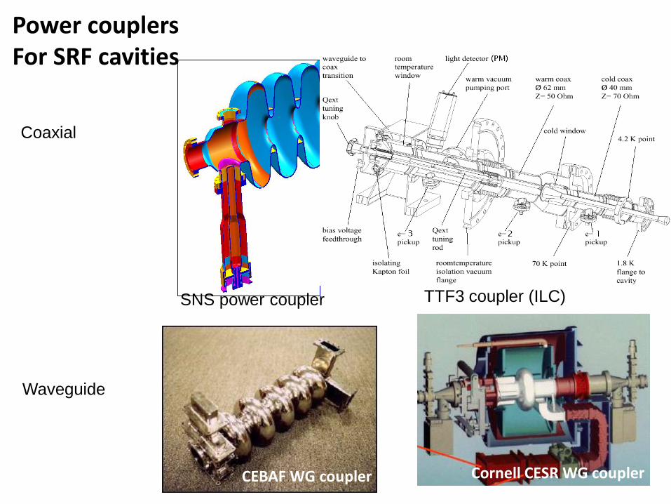
TTF3 coupler (ILC) SNS power coupler
Coaxial
Waveguide
Power couplers For SRF cavities
CEBAF WG coupler Cornell CESR WG coupler
Coupler conditioning
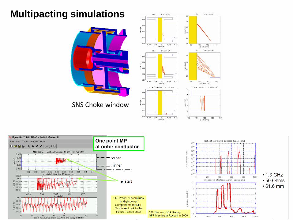
Multipacting simulations
SNS Choke window
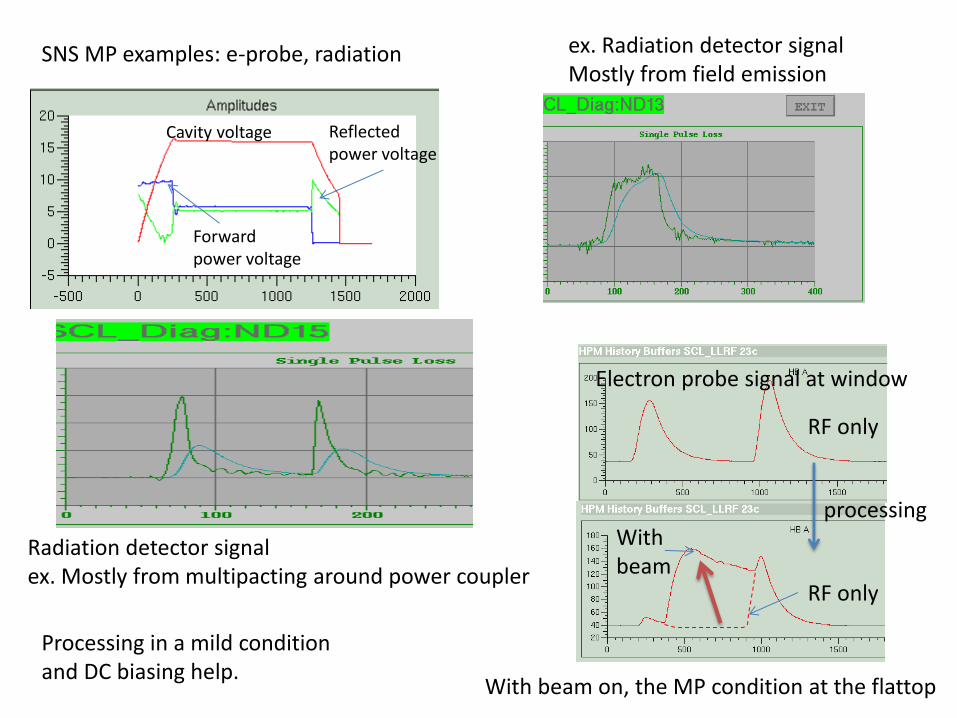
SNS MP examples: e-probe, radiation
Cavity voltage Reflected power voltage
Forward power voltage
ex. Radiation detector signal Mostly from field emission
Radiation detector signal ex. Mostly from multipacting around power coupler
processing
With beam on, the MP condition at the flattop
Electron probe signal at window
RF only
RF only
With beam
Processing in a mild condition and DC biasing help.
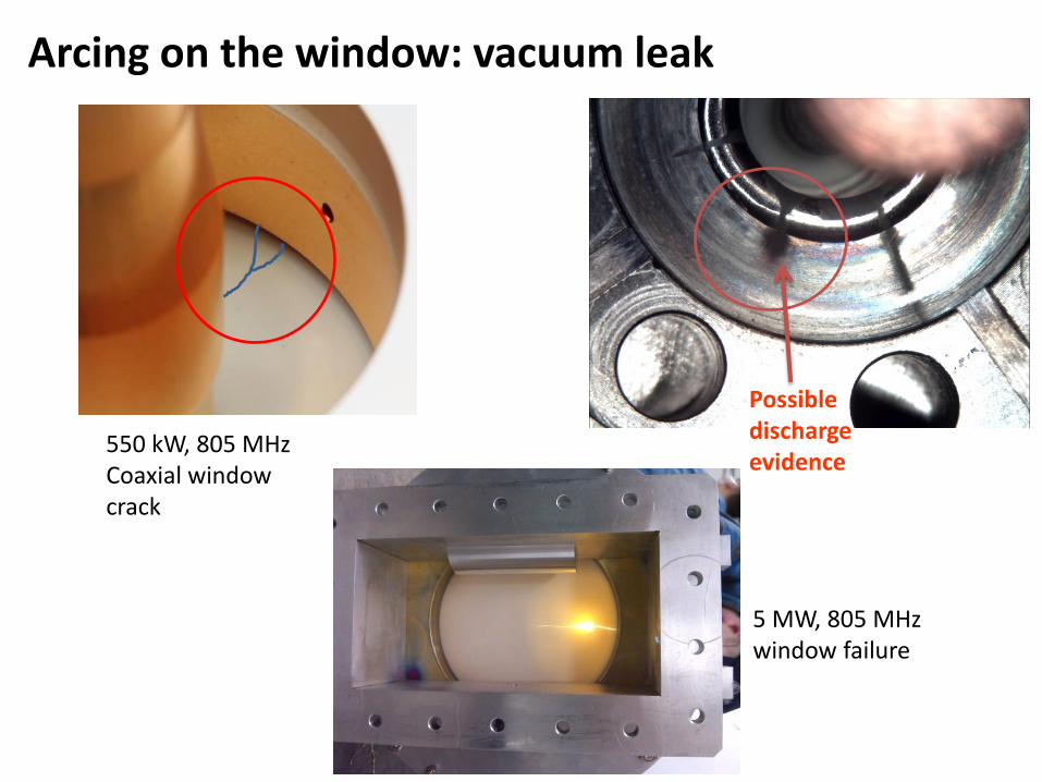
Arcing on the window: vacuum leak
Possible discharge evidence
5 MW, 805 MHz window failure
550 kW, 805 MHz Coaxial window crack
Enhanced Counter Function (20 impacts)
1,E+02
1,E+03
1,E+04
1,E+05
0 5 10 15 20 25 30
Eacc(MV/m)
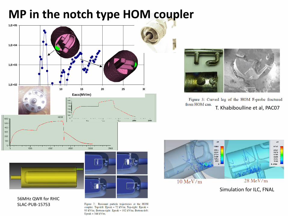
MP in the notch type HOM coupler
T. Khabiboulline et al, PAC07
Simulation for ILC, FNAL
56MHz QWR for RHIC SLAC-PUB-15753
Again in order to avoid MP One can carefully design the RF geometry to avoid MP. If the surface is not clean enough, still there are chances especially if geometry is complex. Analysis may not cover all details. Also if geometry is complex, cleaning would be very difficult. Usually MP could be processed out by careful conditioning/processing. But not always. If there’s not enough diagnostics (blind conditioning), arcing or catastrophic failure could be followed. When arc detector detects an arc or e-probe shows abnormal signals, careful conditioning would be required (a single arc could damage surface). Conditioning at short pulse, low duty helps (sometimes very time consuming). Initial conditioning without DC biasing is preferable if possible.
SNS Examples
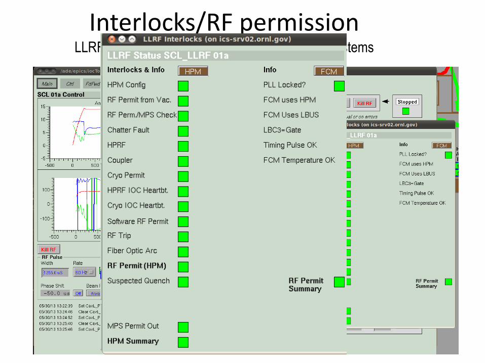
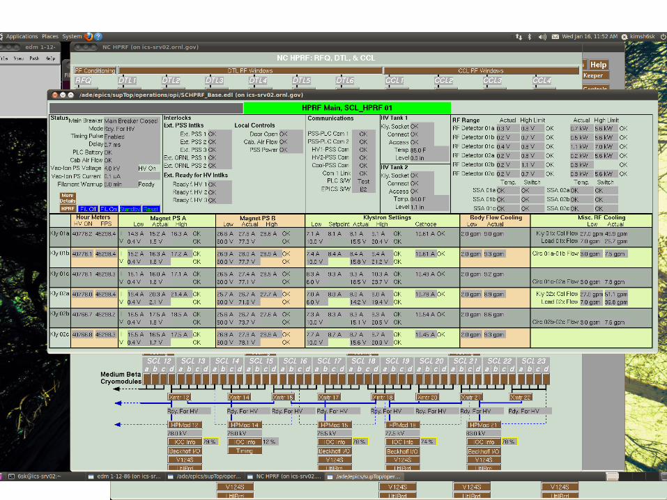
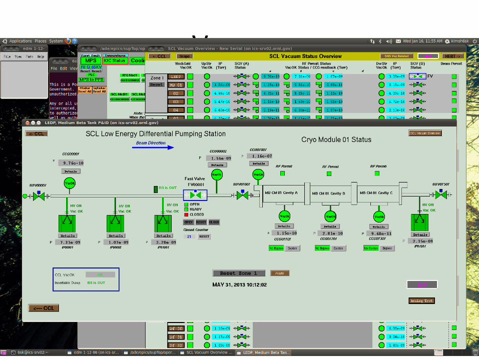
Interlocks/RF permission LLRF system collect all permissions from other systems
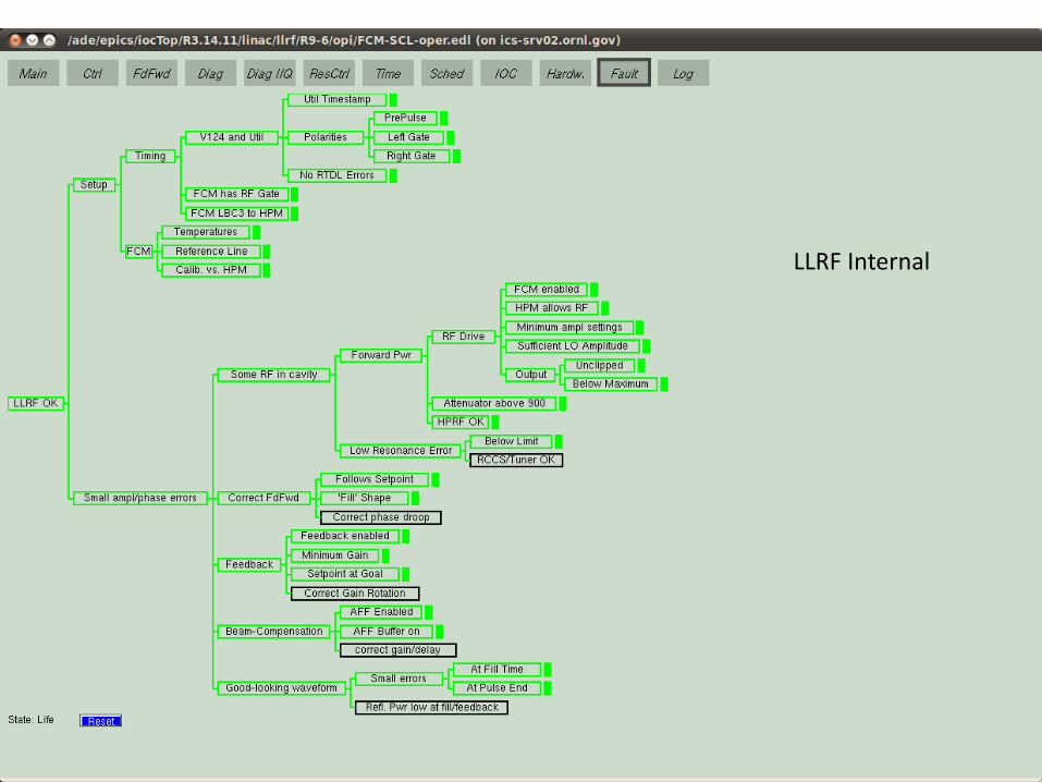
LLRF Internal
HPRF
Vacuum
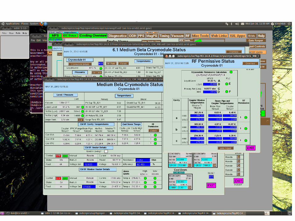
Cryo
LLRF diagnostics buffer
Ex. HPRF system instability
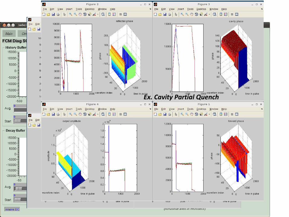
Ex. Cavity Partial Quench

Discussion & Question