Embed Size (px)
Citation preview
Machine Vision and Applications (1995) 8:85-100 Machine Vision and Applications �9 Springer-Veflag 1995
Proteus: a reconfigurable computational network for computer vision Robert M. Haralick, Arun K. Somani, Craig Wittenbrink, Robert Johnson, Kenneth Cooper, Linda G. Shapiro, Ihsin I". Phillips, Jenq-Neng Hwang, William Cheung, Yung Hsi Yao, Chung-Ho Chen, Larry Yang, Brian Daugherty, Bob Lorbeski, Kent Loving, Tom Miller, Larye Parkins, Steve Soos
Department of Electrical Engineering, ~T-10, Applied Physics Laboratory, HN-10, University of Washington, Seattle, Washington 98195, USA
Abstract. The Proteus architecture is a highly parallel, multi- ple instruction, multiple data machine (MIMD) optimized for large granularity tasks such as machine vision and image pro- cessing. The system can achieve 20 gigaflops (80 gigaflops peak). It accepts data via multiple serial links at a rate of up to 640 MB/s. The system employs a hierarchical recon- figurable interconnection network with the highest level being a circuit-switched enhanced hypercube, serial interconnection network for internal data transfers. The system is designed to use 256 to 1024 RISC processors. The processors use 1-MB external read~write allocating caches for reduced multipro- cessor contention. The system detects, locates, and replaces faulty subsystems using redundant hardware to facilitate fault tolerance. The parallelism is directly controllable through an advanced software system for partitioning, scheduling, and development. System software includes a translator for the INSIGHT language, a parallel debugger, low- and high-level simulators, and a message-passing system for all control needs. Image-processing application software includes a variety of point operators, neighborhood operators, convolution, and the mathematical morphology operations of binary and gray-scale dilation, erosion, opening, and closing.
Key words: Proteus - INSIGHT - Reconfigurable compu- tational network - MIMD - Enhanced hypercube - Parallel computing
1 Introduction
A variety of parallel architectures can be used for image pro- cessing applications. To cut short the review of these architec- ture types, we point out some political parallels that have been informally made by some noted researchers. The array can be likened to a Fascist dictator leading a march. The pipeline can be likened to a capitalist assembly line. The pyramid can be likened to the cell block hierarchy of Communist dictatorships; the multiprocessor systems, to parliamentary committees at
Correspondence to: R.M. Haralick
work, and the network, to political anarchy. And the recon- figurable network just cannot get its act together. Particular examples of these architectures include processor arrays such as Illiac IV, CLIP4, CLIP7, DAP, MPP, and GAPE systolic ar- rays such as WARP, pipelines such as Cytocomputer, Genesis, and VAP and multiprocess or systems such as PASM, POLYP, ZMOB, GOP, PICAP, TOSPICS, DIR FLIP, PM4, and pyra- mid systems. Scholarly reviews of these architectures can be found in the papers discussed in [6].
The purpose of this paper is to discuss an architecture in which the act of the reconfigurable network can be put together for computer vision in a large-grain parallelism mode. We do this in the context of knowing that reconfigurable networks for image processing have not been used and that there has been little discussion of architectures that are simultaneously suitable for low-level image processing, high-level computer vision, and the computational tasks required to direct robots and material handlers. All this must be done in near real time in the factory setting.
Our viewpoint differs from the usual discussions of com- puter architecture. We believe that all paradigms that map image data onto processors like the arrays and pyramids, or paradigms that map specialized tasks onto various processors (such as the multiprocessor systems), must, of necessity, cre- me specialized and inflexible systems. We believe that the watchword of computer vision is flexibility. There must be the image-in and image-out operations of low-level vision. There must be the image-in and data structures-out operations of mi- dlevel vision. There must be the data structures-in and data structures-out operations of high-level vision. The purpose of any computer vision system is to be economically useful in the factories of the society in which it functions. Therefore, there must be the capability for performing numerical calcu- lations, data formatting operations, communication reporting operations, and real-time control of external devices such as material handlers and robots. This suggests that the approach must be integrated. To approach the design, we must step back and understand that the low-level neighborhood operators dis- cussed in today's archival literature can be much more com- plex than the Roberts and Sobel variety. We must understand

86
that the manipulation and processing of the high-level vision data structures may be as complex as the symbolic processing required by artificial intelligence computation.
Within our universe, where can we take a stand so that our viewpoint can unravel the inherent complexity of this question of computer vision? The required flexibility suggests that the architecture should be able to execute algorithms of a general nature naturally. The quantity of data processed in a computer vision system suggests that it seeks a higher input rate and that the architecture must be, in some sense, optimized to spend a substantial amount of its processing time doing uniform pixel pushing. If it can have high efficiency in performing a regu- lar pattern of operations on a large data set, it can afford to have a lower efficiency in performing less regular operations on small data sets. In other words, the architecture must spend its time performing a variety of activities. If it can configure itself so that it has high efficiency for the most computation- ally intensive activities, it can afford the overhead required to reconfigure itself for the less computationally intensive and more irregular activities. High efficiency for computationally intensive activities suggests, as one alternative, the algorithm- driven systolic network. Flexibility suggests reconfigurability The combination of the two suggests a dataflow architecture, a reconfigurable network capable of systolic or nonsystolic computation.
However, the kinds of data units that are processed in com- puter vision change as the processes proceed from a low to a high level. Pipelines and systolic architectures that are opti- mized for the pixel data unit are not efficient for midlevel data such as the digital arc, or high-level data units such as a set of corresponding model-image feature points. This suggests that, instead of thinking that the architecture processes small data units such as a pixel, we can visualize an architecture that processes more complex data units such as the image, digital arc, sets, and relations. Here the idea of systolic computation must dissolve, for the units are too large.
In factory applications of machine vision, the same vision algorithm is applied repeatedly to a succession of images. The input is not an image, but a sequence of images. The output to each image processing operation, likewise, is a sequence of images. The clock tick of the systolic array or video rate pipeline gives way to the time chunk taken to process an entire image. The processor, instead of only processing one simple operation such as an add or multiply on the primitive data unit, now must perform an arbitrarily complex sequence of operations on the large data unit. The code run on the processor now does not have to be the kinds of specialized code used for vector processor, pipelines and systolic arrays, or digital signal processors. Rather, the code can be the same kind of code written in languages such as C or Ada and can be tested on standard workstations.
For a high input-data rate and simple algorithms, such an architecture runs in a single program, multiple data-stream mode. For a low input-data rate and highly complex algo- rithms, such an architecture can reconfigure itself to function in a pipeline network or full multiple instruction multiple data
(MIMD) stream mode. We call this architecture the reconfig- urable Proteus architecture.
To understand what must go into the Proteus dataflow ar- chitecture, we must have a language in which to discuss its configuration possibilities. Hardware programming languages like VHDL or N2 and graph description languages are at too low a level. The interesting thing about the data flow in a net- work is that a high-level specification of the configuration of the network is a specification of the program the network is executing. This is different from von Neumann architectures in which a specification of the architecture says nothing about what program may be executing on the hardware. Now, low- level specification of a network, or more formally, a graph having labeled arcs and nodes, has nothing about it that is sequential or procedural. Likewise, a high-level specification need not be sequential or procedural. A high-level specifica- tion of a network is just a specification of the relations that hold in the network. Thus, the specification of the configuration of a network amounts to specifying relations, and since the specifi- cation is the program that the network executes, the language used to program a dataflow network is naturally a language of relations. The language must be inherently nonprocedural. From a high-level perspective, the semantics of the language specifying a computational network describes the essence of the architecture.
In Sect. 2 of the paper, we describe what we mean by a reconfigurable computational network and its underlying dis- tributed control mechanism. In Sect. 3, we describe the lan- guage INSIGHT, a language in the LUCID family of dataflow languages [22], which we have developed to be used both for specification of dataflow architecture configurations, and for the high-level expression and coding of our computer vision algorithms. In Sect. 4, we describe the system software and in Sect. 5, we describe the architecture from a hardware point of view.
2 Reconfigurable computational network
In this section, we give a perspective of the reconfigurable computational network that emphasizes those aspects of the computation that the network must handle and about which a programmer using the network does not have to think. Such a perspective illuminates the division of the hardware domain from the software domain. It provides the hardware-software interface conventions by which the semantics of the language INSIGHT can describe the essence of the architecture of the reconfigurable computational network.
The operation of a reconfigurable computational network involves the flow of sequences of high-level data units through a network of architectural primitives. Architectural primitives are of two types: processors and connections. Processors have one or more inputs and one or more outputs. They produce high-level data units of the same or different kind than the input data units for output lines after some finite execution time. The amount of time taken to execute may be proportional to data unit size, or it may be worse than linear time, as it might be for a search algorithm.
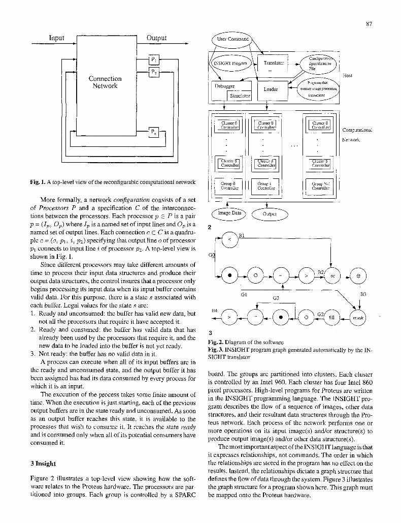
Input
Connect ion Network
Output
i I
Fig. 1. A top-level view of the reconfigurable computational network
More formally, a network configuration consists of a set of Processors P and a specification C of the interconnec- tions between the processors. Each processor p G P is a pair p = (Ip, Op) where Ip is a named set of input lines and Op is a named set of output lines. Each connection c E C is a quadru- ple c = (o, pl , i, P2) specifying that output line o of processor Pl connects to input line i of processor p2. A top-level view is shown in Fig. 1.
Since different processors may take different amounts of time to process their input data structures and produce their output data structures, the control insures that a processor only begins processing its input data when its input buffer contains valid data. For this purpose, there is a state s associated with each buffer. Legal values for the state s are: 1. Ready and unconsumed: the buffer has valid new data, but
not all the processors that require it have accepted it. 2. Ready and consumed: the buffer has valid data that has
already been used by the processors that require it, and the new data to be loaded into the buffer is not yet ready.
3. Not ready: the buffer has no valid data in it. A process can execute when all of its input buffers are in
the ready and unconsumed state, and the output buffer it has been assigned has had its data consumed by every process for which it is an input.
The execution of the process takes some finite amount of time. When the execution is just starting, each of the previous output buffers are in the state ready and unconsumed. As soon as an output buffer reaches this state, it is available to the processes that wish to consume it. It reaches the state ready and is consumed only when all of its potential consumers have consumed it.
3 Insight
Figure 2 illustrates a top-level view showing how the soft- ware relates to the Proteus hardware. The processors are par- titioned into groups. Each group is controlled by a SPARC
Group 0 ControIler Group I I Controller
o ~ 1 7 6
Group N-I Controller
87
Host
Computational Network
2
G ~ B I
) G1 G3 ~ B3
\ r W k J U/ . I m a ~)
3
Fig. 2. Diagram of the software Fig. 3. INSIGHT program graph generated automatically by the IN- SIGHT translator
board. The groups are partitioned into clusters. Each cluster is controlled by an Intel 960. Each cluster has four Intel 860 pixel processors. High-level programs for Proteus are written in the INSIGHT programming language. The INSIGHT pro- gram describes the flow of a sequence of images, other data structures, and their resultant data structures through the Pro- teus network. Each process of the network performs one or more operations on its input image(s) and/or structure(s) to produce output image(s) and/or other data structure(s).
The most important aspect of the INSIGHT language is that it expresses relationships, not commands. The order in which the relationships are stored in the program has no effect on the results. Instead, the relationships dictate a graph structure that defines the flow of data through the system. Figure 3 illustrates the graph structure for a program shown here. This graph must be mapped onto the Proteus hardware.
88
A typical program:
function Detect (integer array[256, 256] GO;) (binary array[256, 256] B4;)
where declare
integer array[256, 256] G1,G2,G3; binary array[256, 256] B 1,B2B3; integer constant T1=195,T2=20,T3=25; integer constant W 1 =5 ,W2= 15,W3 =42 ,W4= 126 ,W5--3;
relations B1 = G0<T1; G1 -- GO closedby box(W1,W1); B2 = (G1 - (G1 openedby box(W2,W2)))>T2; B3 = (B1 or B2) dilatedby box(W5,W5); G2 = fill(G1 maskedby B3); G3 = G2 openedby box(W3,W3); B4 = (G3 - (G3 closedby box (W4,W4)))>T3;
endwhere
The input to this INSIGHT program is a 256 x 256 gray- scale image GO, and the output is a 256 x 256 binary image B4. Intermediate gray-scale images G1, G2, and G3 and the intermediate binary images B 1, B2, and B3 are also produced during the execution of the program. The first relation says that gray-scale image GO is to be thresholded using threshold T1 (a constant), and the result is to become binary image B 1. The second relation says that GO is also to be the input to a morphological closing operation [8] with a structuring element that is a box (rectangle) of dimension 5 • 5, with the result becoming gray-scale image G1. The third relation specifes the production of another binary image B2 that is the result of performing an opening in G 1, subtracting the opening from G1 itself, and thresholding the result of the subtraction. The other relations can be analyzed in a similar fashion.
The INSIGHT translator maps the algorithm onto the hard- ware. The INSIGHT translator has two main parts: the scan- ner/parser module and the linker/partitioner module. The scan- ner/parser module uses standard translation techniques. It em- ploys a finite machine for lexical analysis and a recursive de- scent parsing mechanism with look-ahead by one, augmented by a precedence parser for expression. The output of the scan- ner/parser module goes to the linker that replaces single nodes of the graph representing INSIGHT library routines by pre- stored subgraphs that came from previous translations. Also, nodes representing morphological operations that use possi- bly complex structuring elements may be decomposed into sequences of nodes that use smaller structuring elements [22]. This decomposition is beyond the scope of this paper. The par- titioner is the only nonstandard part of the translator. Its job is to map the operations in the final dataflow graph onto the reconfigurable network. The goal is to produce the mapping with the highest throughput, so that as much data as possible can be handled by the reconfigurable network.
The problem of the partitioner can be stated as follows. Given a dataflow graph with k nodes with an estimation of the amount of processing time each takes, and a multiproces-
sor shared memory system with Npro~ processing elements, with a specified interconnection network and interprocessor communication costs, determine how the operations must be partitioned among the processors to gain maximum through- put. Initially we chose a greedy technique as in [1].
To control the load balancing, each processor has all of the nodes it will process assigned to it. The algorithm keeps a list of all nodes that have had all of their ancestors allocated. This is called the ready list. A heuristic is generated for each of the nodes in the ready list at each step, estimating the cost of assigning that node to the current processor. The heuristic is based on the expected computation time of the node, the load so far on the processing block, and the communication required by assigning this node to this processing block. The lowest heuristic cost is assigned to the processor, a new ready list is determined, and the process repeated until no node has a heuristic below a threshold value. At this point, nodes are assigned to the next processing block.
After allocating the nodes in this fashion, a relaxation pro- cedure is used to determine if one or more nodes can be shifted between processors to lower the maximum load. The first step of this procedure is to determine which processing element has the largest load of computation + communication determined by
L(max) = max Z(t i ,~ + Ci,~) (1) ~ = I . . . . . Nprnc i=1
where Nproc is the number of processors, N~ is the number of nodes assigned to the nth processor, ti,~ is the computation time of the ith node assigned to the nth processor, and c~,~ is the communication time required by the nth processor due to the ith node.
When the processor with the largest load has been deter- mined, then each node assigned to that processor is checked to see if it can be moved to the previous or the next processor. A node can be moved to the previous processor if none of its input arcs are generated by nodes on the processor to which this node is currently assigned. Similarly, a node can be moved to the next processor if none of its output arcs are consumed by nodes on the processor to which this node is currently as- signed. If a node can be moved, then the new maximum load (see Eq. 1) that this new assignment would create is calculated. If this new maximum load is less than the current maximum load, then the movement that reduces the new maximum load is taken, and the process is repeated. If none is found that reduces the maximum load, then the relaxation is complete. Two methods of selecting the modification have been used: (1) The maximum optimization rule: the node that lowers the maximum load the most is selected, and (2) the minimum dis- turbance rule: the node that lowers the maximum load the least is selected.
The low-level software support for the high-level program- ming environment is the processing library. As an example, the image-processing library contains the processor code for the operations in the INSIGHT application program. Each image- processing operation in the following is a verb in INSIGHT.
The initial set of functions in the library include arithmetic and logical operations on images, geometric spatial transforms, convolution and morphological operations, neighborhood op- erations, connected components, and masking.
In the Proteus system, users are allowed to choose the number of processors among which they wish to partition the algorithm. This partition is then replicated with successive inputs images routed to successive processor blocks until all processors have been used.
4 System software
The system software consists of a loader and debugger running on the Proteus host, message processing and control modules running the group and cluster controllers, and an interrupt han- dler that is the only system-level software resident on the pixel processors.
4.1 Loader
As specified by the INSIGHT program and the number of processors the user chooses to use for each task, the translator generates an assignment file. Each assignment file defines a set of generic processors and the job partitions between them. Each assignment fiIe defines a task class. The Proteus system can execute multiple instances of a single task class or single instances of multiple task classes.
The user issues a task(s) request to the host to start load- ing and task execution. A task(s) request indicates which task class(es) should be executed, the external data sources for each task class if they need to be defined. As specified by the user's task(s) request, the loader retrieves the assignment file(s) pro- duced by the translator. It determines if the Proteus hardware is capable of executing the specified assignment. If all is well, the loader performs the mapping of the logical processor names in Proteus to the symbolic processor names used by the trans- lator to define the generic processor set. The mapping can be many-to-one or one-to-one. Physical processors are the true working horses for computation. For reasons of flexibility and fault tolerance, the loader does not assign jobs to physical pro- cessors directly. The cluster controller has that responsibility. At run time, it makes a one-to-one mapping between a logical processor name and the true physical processor.
Throughout the system, the logic and physical mapping is decided hierarchically. The host decides the mapping between the logical groups and the physical groups. Each group con- troller decides the mapping between logic clusters and physical clusters. Each cluster controller assigns physical processors to logic processor names. The containing relationships between logical processors, logical clusters, and logical groups are pre- defined, i.e., a logical processor belongs to a certain logical cluster, which, in turn, belongs to a certain logical group.
Each logical processor inherits the assignments from its corresponding symbolic processor. According to the inheri- tance relationship, each logical processor has a list of jobs to be executed. Each job contains the following attributes:
89
program_id, input_arcs, output_arcs, and constant parameters. Each job has a uniqe identification assigned by the loader. Each arc has a unique arc identification assigned by the loader. Buffers are assigned to each arc. How many buffers should be assigned is decided by the translator. The cluster controller assigns actual memory addresses to each buffer.
The loader packs all the schedule information needed by a logical cluster into a scheduling file and all the constant param- eters needed by the jobs executing within that logical cluster into a constant file. At run time, the cluster controller transfers task scheduling information from the cluster to the pixel pro- cessor via a task control block. The task control block contains the identification tag, starting address of the program to be ex- ecuted by the pixel processor, and pointers to the buffers to be used for input and output. According to the jobs assigned to the logical pixel processors with each logic cluster, the loader determines which programs should be loaded to that cluster and assigns memory space in shared memory to each program. Then, the loader creates a transfer request file for each group. Each transfer request file has a list of file transfer requests. Each request has the following format:
<request> := <source> <destination list> <source> := <file_name> <file_size> <file_name> := full path name of the file to be transferred <destination_list> := <destination> I <destination> <destination_list> <destination> := <logic_cluster_name> <physical_starting_address> After all the required files are generated properly, the host
uses the socket facility of the Unix system to send a load- ing request to each group via Ethernet. Each request includes two parts. The first part specifies that the action is loading. The second part is the full path name of the transfer request file. According to the message received, each group controller retrieves the transfer request file through the network file sys- tem (NFS) from the disk. Each group controller reads in its file specified in the request file, writes it to the VME buffer of the destination cluster(s) and requests the destination cluster controller to move it to the shared memory starting from the physical address specified in the request file. The cluster con- troller uses the check sum stored in each file to check for any transmission errors.
When all the files specified in the transfer request file have been moved to the clusters, the group controller sends a file transfer complete message to each cluster in the group. If the file-transfer-complete messages have been received, every file is properly stored, and every processor in the group is ready to work, the cluster controller sends a ready-to-work message to the group controller. After receiving a ready-to-work message from all the clusters wihin the group, the group controller sends a ready-to-work signal to the host. After receiving the ready- to-work message from all the groups, the host synchronizes the external data sources, and the Proteus system begins the task(s) execution.

90
Processor A Processor A Reception Transmit
Buffer State
Message Header
BuHerState
Message Header
D A T A
Processor B Processor B Transmit Reception
Fig. 4. Message buffer layout
4.2 The communication system
The processing and computation in Proteus use a variety of software and hardware control mechanisms. Each pixel pro- cessor in a cluster and the cluster controller have shared- memory mail boxes. They also communicate with each other via interrupts. At run time, the cluster controller dispatches a job to each idle pixel processor by putting the job in the task control block and interrupting the pixel processor to indicate that the task control block is ready to be read. When a pixel processor finishes its assigned job, it creates a task completion record and interrupts its cluster controller to report the results. After receiving the interrupt signal from the pixel processor, the cluster controller reads the completion record to get the in- formation trom the pixel processor, updates the status of data regions due to the task just completed, and continues to acti- vate sleeping processors. When a busy processor completes a task, it consults its task control block area to determine its next task. In this manner, busy processes do what they have to do without ever having to be interrupted once they begin their pro- cessing. If all tasks in the processor's task control block have been completed, the pixel processor will interupt the cluster controller with the run completion message and put itself to an idle state.
All messages passing between processors consist of copy- ing the message (header and data) from the source-processor memory to a memory location that the receiving processor can access. This memory is accessed in a synchronized manner to prevent confusion. The sending processor and receiving pro- cessors view the buffer in a complementary fashion as shown in Fig. 4.
In Fig. 4, processors A and B are shown sharing a set of message buffers. Notice that the Processor B Transmit buffer is the processor A reception buffer and vice versa. Data from A to B are copied into the buffer shown on the right and data from B to A are copied into the buffer on the left.
The general steps processor A goes through to send a mes- sage to Processor B are: 1. Processor A checks its transmit buffer state and if in the
unread state waits until a later time to send the message.
2. When the buffer state is set to read by processor B, proces- sor A has control of the contents of the processor A transmit buffer. Processor A then cupies both the header and the data of the message into the processor A transmit buffer.
3. Processor A then sets the buffer state to unread, indicating a new message is in the buffer.
4. Processor A completes its portion of the message transfer by interrupting processor B to cause it to check its reception buffer. When a processor B receives a message, it performs the
following processing: 1. It receives an interrupt that causes the processor to stop
its current processing and check to see if it has received a message.
2. The message check consists of making certain its reception buffer is in the unread state.
3. When processor B has finished with the reception buffer (either by copying it into a local buffer or processing it directly), it sets the buffer state to read. Finally, to provide an aid for execution tracing that can be
used in performance monitoring, tuning, and debugging, the Proteus system software has been provided with the portable instrumented communication library (PICL) developed by Oak Ridge National Laboratory [8, 9, 12]. The PICL commu- nication library was originally developed to provide portability and easy parallel program development. It has a good facility for execution tracing, which is its major use in Proteus.
4.3 The debugger
The debugger of the Proteus system is implemented as two communicating processes, one on the host and the other on the Proteus system. The debugger interacts with the user through the host's window system. It has the capability of supporting the development of system and application programs. The de- bugger provides the user with the capabilities of controlling and monitoring the execution of all the pixel processors in the Proteus sytem. Therefore, the user must have full knowledge of the system architecture, how the system operates, and its physical sources of input images during the run time.
On the host, the debugger is simply a graphical user in- terface (GUI) that interacts with the user, and manages the bulk of debugging information (e.g., symbol tables) that al- lows it to map symbolic information to physical addresses in the hardware. However, the physical laydown of code break- points, memory accesses, and modification of processors' exe- cution states must be done by system services provided by the cluster controllers and the pixel processors from the hardware side.
Along with the execution of the hardware, the debugger is also in control of three other system applications on the host. They are the loader, the high-level simulator, and the low-level simulator. Each of them supports the debugging of image processing application programs at a different level.
At the application level, the subject language is INSIGHT. At this level, the debugger allows the user to control execu- tion by setting image watchpoints (i.e, data breakpoints) in

91
the INSIGHT dataflow graph. When a pixel processor picks up a task that will be producing an output image associated with an image watchpoint, it is interrrupted and the debugger takes control of its execution. At this debugging level, the user can invoke the high-level simulator to execute the correspond- ing INSIGHT program. The simulator, which also runs on the host, will produce a trace of images that can be compared to those that are generated by the hardware. To allow the user to visualize the results, the debugger can compare two images and display the corresponding images in a window.
At the system level, the subject language is the assem- bly language of the i860 pixel processor. The user may trace through the execution of a program by a pixel processor by setting code breakpoints inside the program and single step- ping through the program. The user may invoke the low-level simulator to execute this program in the same sequence that would be executed in the hardware. By comparing the execu- tion states of the pixel processor against those generated by the simulator at Certain points of the course of execution, the debugger is able to locate any error that could occur.
The high-level simulator, written in ADA and executed on the SparcStation host, is designed to verify that INSIGHT algo- rithms and the Proteus image-processing library are correctly implemented in Proteus. Under the control of the Proteus de- bugger, the high-level simulator executes vision algorithm that are exactly the same algorithms executed by the Proteus hard- ware. A comparison between the two results can then provide information about the correctness of Proteus's result.
There are three major components in the high-level sim- ulator: a debugger interface, a controller, and an application library. The debugger interface parses the command line for the simulator passed down from the debugger. The controller figures out the appropriate tasks to carry out while the ap- plication library is accessed by the controller for the number crunching. The high-level simulator can be instructed to start a new application by loading in an INSIGHT program. It is able to find the exact steps involved in performing the cal- culation for each node in the INSIGHT dataflow diagram. It also provides a session-save feature so that intermediate re- sults and system status can be loaded back into the system in a future session with the session-reload capability. Although it functions under the control of the Proteus debugger, the high- level simulator is a full-fledged image-processing system on its own.
Graphical user interface. The GUI was developed under an X Window-based platform called the transportable application environment (TAE). It has: 1. One master control window that allows users to set/change
the debugger context at the cluster level and to view the INSIGHT source subject to the debugger session
2. One cluster control window that allows users to control the execution of the dataflow graph associated with the subject INSIGHT program
3. One processor control window that allows users to control the execution of particular application program in sequen- tial fashion
4. A number of pop-up windows that prompt for user inputs
The debugger is a mouse-driven system that takes input parameters from the keyboard for some debugger functions. Through the GUI, users can view the updates of the program state and control program execution conveniently during a de- bugger session.
Set image watchpoints. In a debugger session, when the user suspects that the output image of a primitive operation is not correct, he/she may switch the debugger context to the asso- ciated cluster in which the image is generated and establish a watchpoint on the image. The debugger maps the symbolic name of the image to a logical identification number. Then the debugger processes the schedule file corresponding to the designated cluster and determines all the physical identifica- tion numbers associated with that image in the context cluster. Finally, the debugger marshalls the destination address of the cluster and the physical identification numbers into a debugger message and delivers it to the cluster controller of the desig- nated cluster.
When the cluster controller receives the debugger message, it checks all the task control blocks in the cluster, tagging those of the designated output images. The tag tells the microproces- sor that picks up the task control block to stop execution once after it has picked up the task. At that time, the corresponding microprocessor is under the control of the debugger; it polls for debugger messages from the host and acts as requested. The microprocessor remains under the control of the debug- ger until a debugger message tells it to resume execution.
The list of possible user requests include: 1. Set data breakpoint on any particular memory location. 2. Set code breakpoints in the assembly program associated
with that task. 3. Peek and modify the contents of specific image pixels or
registers. 4. Probe for the execution status of the microprocessor. 5. Single step through the program. 6. Resume the execution of the assembly.
Therefore, when the user wants to trace the execution of a particular program that might produce an erroneous image he/she is interested in, he/she must set an image watchpoint on that image before the execution of the INSIGHT algorithm gets to that point.
Furthermore, the user is also allowed to remove any image watchpoints that have been established in a debugger session. The debugger puts the physical identification numbers asso- ciated with the specified image into a debugger message. The message is delivered to the subject-cluster controller, which then removes the watchpoint tags from the associated task control blocks. Their output images are identified by those numbers enclosed inside the message.
Code breakpoints. In the debugger, code breakpoints can be established in and removed from application programs dur- ing a debugger session. The implementation of breakpoints illustrates the division of labor between the two components of the debugger. Based on user commands and symbol table information, the host component is responsible for deciding
92
where breakpoints are located and maintains a list of break- point records for each application program. For each request, it sends a debugger message to the interrupt handler of the designated processor, which is responsible for laying down the software trap instruction and then later restoring displaced instructions, as the user requests the removal of the associ- ated breakpoints. It is also the responsibility of the interrupt handler to maintain the finer details of the state of the sub- ject program. If the subject prograin is to be resumed from a halt at a breakpoint, the interrupt handler knows that it must back up and single step the lost instruction, before re-laying the breakpoints and restarting the subject program.
In the debugger, code breakpoints are implemented via the software breakpoint mechanism. A code breakpoint can be established in a program by replacing the 4-byte object code of the instruction at the designated program location with that of the software trap instruction. This modification is done directly by the interrupt service routine on the copy of the application program that is stored in the shared memory of the context cluster.
Some features of the i860 microprocessor impose con- straints on the establishment of breakpoints in application pro- grams. There are three constraints: 1. Breakpoints cannot be established at floating point instruc-
tions that will be executed in dual instruction mode. 2. No breakpoint may be established at the next instruction
that follows a delayed branch instruction in single instruc- tion mode.
3. No breakpoint may be established at the next three instruc- tions that follow a delayed branch instruction in dual in- struction mode. The first constraint is due to the dual instruction mode
in the i860 microprocessor, in which the integer core unit and floating point unit can execute instructions in parallel. This ca- pability is supported by an instruction-fetch unit that can fetch two consecutive instructions (one integer instruction and one floating point instruction) at the same time. During execution in dual instruction mode, the instruction sequence consists of eight-byte aligned instructions with a floating-point instruc- tion in the lower four bytes and a core instruction in the upper four bytes. However, the software trap instruction is defined in the core instruction set. The result of placing a core instruc- tion in the lower four bytes of any instruction sequence that would be executed in dual instruction mode is undefined. An error may occur when the floating point unit decodes the core instruction, as if it were a floating point instruction.
The second constraint is due to the pipelined execution of instructions in the processor. In the delayed branch mecha- nism, the instruction that follows the delayed branch instruc- tion in the program will be executed regardless whether the branch is taken. If this instruction were replaced by a software trap instruction, the processor would still be interrupted at that location, but the delayed branch mechanism would have been broken and the execution states could have been changed after the interrupt. Therefore, it is impossible to resume the program execution from the breakpoint location because the branch in- struction has already been executed before the interrupt. As a
result, the second constraint is imposed. The third constraint is implied by the first two constraints.
Based on these three constraints, the debugger builds up a code table for each of the application programs involved in the INSIGHT algorithm. The code table of an application program is a hash table of records containing the offset address and object code of instructions at which brakpoints can be established without violating the three constraints. When the user wants to set a breakpoint at a particular program location, the debugger will compute the corresponding offset address and looks up the associated code table to determine whether a breakpoint can be established. This mechanism is necessary because the user may mess up the program behavior if he/she is provided with too much freedom to change the application program.
After the offset address of the breakpoint has been deter- mined, the debugger determines the physical address of the associated program in the cluster processor and computes the physical address. It marshalls the physical brakpoint address in a debugger message and sends it to the pixel processor. When the pixel processor receives the message, it simply over- writes the specified memory location with the object code of a software trap instruction. After the operation has been ac- complished, the processor will return an acknowledgement message to the debugger.
Data breakpoint. To provide control of execution for appli- cation programs, the debugger uses a data breakpoint mecha- nism. As code breakpoints are implemented by software, the implementation of the data breakpoint or watchpoint is hard- ware oriented. Each i860 microprocessor has a data breakpoint register, db that supports the implementation of the watchpoint mechanism.
The data breakpoint register monitors the contents of the address bus of the microprocessor. When the i860 micropro- cessor accesses an operand at the address in the data breakpoint register, the register generates a trap that interrupts the execu- tion of the processor. When a trap occurs, control is passed to an interrupt service routine that determines the type of trap by examining the trap bits in the psr register. In this case, ei- ther the instruction-access or the data-access trap bit will be set, depending on whether the operand causing the trap is an instruction or a datum.
The major drawback of using the data-breakpoint regis- ter to implement the watchpoint mechanism is that there is only one data-breakpoint register available per microproces- sor. Therefore, only one watchpoint can be established in an application program at any time, and this obviously cannot satisfy the user's needs.
The user can establish a watchpoint on any memory loca- tion that is confined to the scope of visibility of the application program associated with the pixel processor. It could be one of the following: 1. Any pixel of the input/output images. In this case, the de-
bugger asks the associated cluster controller for the physical address of the designated image buffer, and then computes the physical address of that pixel.
2. Any local variable of the application program. In this case, the debugger finds the offset address of the program vari- able by looking up the program's symbol table and the phys- ical address of the program in question by looking at the corresponding schedule file prepared by the loader. They are then added to get the physical address of the variable.
3. Any physical memory location, as specified by the user. In this case, no address mapping or translation is required because the specified address is already a physical one. After the physical address of the designated memory lo-
cation has been computed by any one of these methods, it is marshalled into a debugger message, which is delivered to the designated microprocessor. Finally, the interrupt handler of the processor places the address in the i860 f db register and sets the BW bit in the psr register to catch any write to that memory location.
In contrast, the removal of a data breakpoint from a pro- gram is simpler. The user simply issues the request and a debugger message is delivered to the designated micropro- cessor. The processor simply turns off the BW bit of the psr and the data breakpoint is deactivated. It must be noted that the db register of every microprocessor is deactivated when it has finished executing an application program because the watchpoint of the current scope cannot be passed on to other programs.
Display-and-modify values. To display or modify the values of image data and program variables as execution proceeds, we need to know where the values are stored and we need to know how to print them. Thus, we need storage and type information for each variable from the compiler. This is usually part of the information kept in the compiler's dictionary, and is generally stored in object files produced by the compiler.
In order for the storage information produced at compile- time to be accurate at run time, the code corresponding to each statement must store current values of variables in the location assigned to them by the compiler. Otherwise, if the current value of the variable is in a register somewhere, but not in the location given by the compiler, we will not get the current value. Some sophisticated debuggers have a list of locations for each variable at various program points, and they are able to tell the users whether the current value of a variable is active in memory or stored in a register at any program point.
There are three data entities that can be accessed by the user. They are program variables, image pixels, and processor's registers. To access a variable defined in the pixel processor's current task, the debugger looks up the variable's offset ad- dress in the symbol table of that application program. Then it determines the program's physical address in the memory shared by the designated cluster processor. The lookup for the offset address of a variable is a 3-tuple operation:
lookup(symbol-table, variable, offset-address)
Then it computes the physical address of the variable, mar- shalls it into a debugger message, and sends it to the pixel processor.
Similarly for accessing image pixels, the debugger asks the pixel processor for the physical address of the associated
93
buffer and the offset address of the specified pixel. Then it computes the physical address of the pixel and sends it to the pixel processor in a debugger message.
When the pixel processor receives a message for memory acccess, it can do one of the following: 1. For the display/operation, it reads the content of the spec-
ified memory location and returns it to the debugger in a message to acknowledge the message it received.
2. For the modify/operation, it extracts a value from the mes- sage, writes it to the specified memory location, and then returns an acknowledgement message in response to the message it received. In this manner, the interrupt service routines need not have
any knowledge of what kind of data they are dealing with. In the case of registers, the access mechanism is different.
When the debugger gains control of a processor, the contents of the processor's registers are marshalled into a single mes- sage and delivered to the debugger by the processor itself. The debugger copies this information from the message to a buffer. Any display or modification request pertaining to an individ- ual register is made to this host's copy. This copy of registers' contents is shipped back to the pixel processor before the de- bugger releases the control of the processor. Then the pixel processor restores the updated values for its registers before it resumes execution.
The pixel processor interrupt handler. The pixel processors do not have an operating system. Each has only an interrupt handler to take care of its system level interactions. By putting as many as possible of the operating system functions with the cluster controller processor, the pixel processor can devote its entire resources to the operation.
The interrupt handler determines and verifies the cause of any trap and takes appropriate action. There are three kinds of traps: reset, external, and software. Whenever a trap occurs, ex- ecution of the current instruction is aborted immediately. The user mode and interrrupt mode are saved in a stack, the pro- cessor goes into supervisor mode, and interrupts are disabled. Then the cause of the trap is determined, and the appropriate action is taken.
On reset trap, the processor performs the boot test, flushes the instruction and data cache, and copies the buffer pointers from the reboot record to the safe storage area in the pixel processor's local memory. After the boot code is executed, the pixel processor sends a reboot done message back to the cluster controller.
If an external trap other than a reset trap is detected, the interrupt handler performs the task specified in the message buffer. After it finishes the job, it sends a return message to the cluster controller. Then the resume address is determined and the process before the interrupt continues. If a software trap occurs, the interrupt handler deterines the cause, takes appropriate action, and resumes execution.
I
94
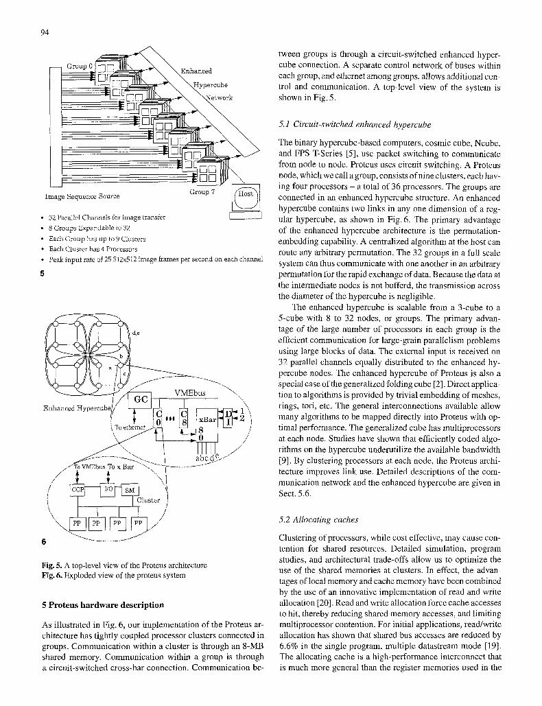
tween groups is through a circuit-switched enhanced hyper- cube connection. A separate control network of buses within each group, and ethernet among groups, allows additional con- trol and communication. A top-level view of the system is shown in Fig. 5.
Image Sequence Source Group 7
�9 32 Parallel Channels for image transfer �9 8 Groups ExpandabIe to 32 �9 Each Group has up to 9 Clusters �9 Each Cluster has 4 Processors �9 Peak input rate of 25 512x512 image frames per second on each channel
d,e
Enha ~ ~ J , ,~MEbus ~ \ i
l// "',
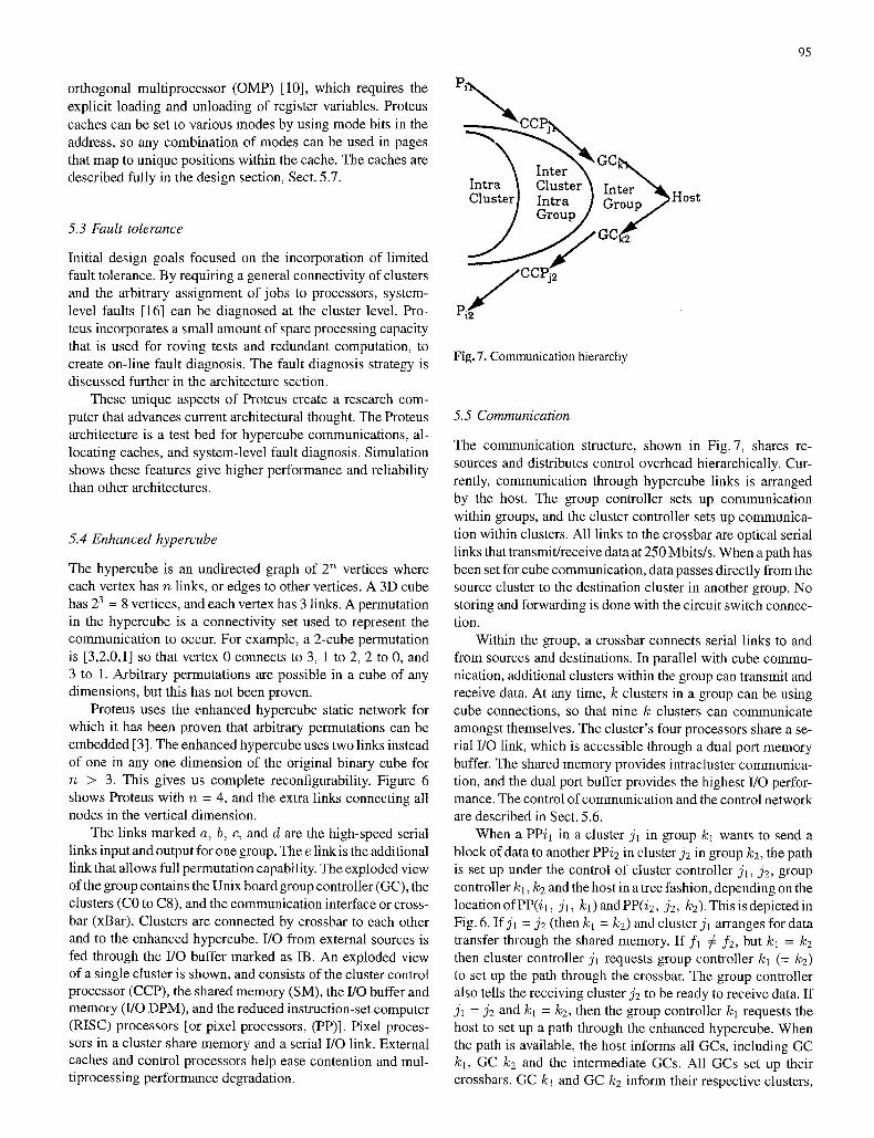
Fig. 5. A top-level view of the Proteus architecture Fig. 6. Exploded view of the proteus system
5 Proteus hardware description
As illustrated in Fig. 6, our implementation of the Proteus ar- chitecture has tightly coupled processor clusters connected in groups. Communication within a cluster is through an 8-MB shared memory. Communication within a group is through a circuit-switched cross-bar connection. Communication be-
5.1 Circuit-switched enhanced hypercube
The binary hypercube-based computers, cosmic cube, Ncube, and FPS T-Series [5], use packet switching to communicate from node to node. Proteus uses circuit switching. A Proteus node, which we call a group, consists of nine clusters, each hav- ing four processors - a total of 36 processors. The groups are connected in an enhanced hypercube structure. An enhanced hypercube contains two links in any one dimension of a reg- ular hypercube, as shown in Fig. 6. The primary advantage of the enhanced hypercube architecture is the permutation- embedding capability. A centralized algorithm at the host can route any arbitrary permutation. The 32 groups in a full scale system can thus communicate with one another in an arbitrary permutation for the rapid exchange of data. Because the data at the intermediate nodes is not bufferd, the transmission across the diameter of the hypercube is negligible.
The enhanced hypercube is scalable from a 3-cube to a 5-cube with 8 to 32 nodes, or groups. The primary advan- tage of the large number of processors in each group is the efficient communication for large-grain parallelism problems using large blocks of data. The external input is received on 32 parallel channels equally distributed to the enhanced hy- percube nodes, The enhanced hypercube of Proteus is also a special case of the generalized folding cube [2]. Direct applica- tion to algorithms is provided by trivial embedding of meshes, rings, tori, etc. The general interconnections available allow many algorithms to be mapped directly into Proteus with op- timal performance. The generalized cube has multiprocessors at each node. Studies have shown that efficiently coded algo- rithms on the hypercube underutilize the available bandwidth [9]. By clustering processors at each node, the Proteus archi- tecture improves link use. Detailed descriptions of the com- munication network and the enhanced hypercube are given in Sect. 5.6.
5.2 Allocating caches
Clustering of processors, while cost effective, may cause con- tention for shared resources. Detailed simulation, program studies, and architectural trade-offs allow us to optimize the use of the shared memories at clusters. In effect, the advan- tages of local memory and cache memory have been combined by the use of an innovative implementation of read and write allocation [20]. Read and write allocation force cache accesses to hit, thereby reducing shared memory accesses, and limiting multiprocessor contention. For initial applications, read/write allocation has shown that shared bus accesses are reduced by 6.6% in the single program, multiple datastream mode [19]. The allocating cache is a high-performance interconnect that is much more general than the register memories used in the
95
orthogonal multiprocessor (OMP) [10], which requires the explicit loading and unloading of register variables. Proteus caches can be set to various modes by using mode bits in the address, so any combination of modes can be used in pages that map to unique positions within the cache. The caches are described fully in the design section, Sect. 5.7.
5.3 Fault tolerance
Initial design goals focused on the incorporation of limited fault tolerance. By requiring a general connectivity of clusters and the arbitrary assignment of jobs to processors, system- level faults [16] can be diagnosed at the cluster level. Pro- teus incorporates a small amount of spare processing capacity that is used for roving tests and redundant computation, to create on-line fault diagnosis. The fault diagnosis strategy is discussed further in the architecture section.
These unique aspects of Proteus create a research com- puter that advances current architectural thought. The Proteus architecture is a test bed for hypercube communications, al- locating caches, and system-level fault diagnosis. Simulation shows these features give higher performance and reliability than other architectures.
5.4 Enhanced hypercube
The hypercube is an undirected graph of 2 n vertices where each vertex has n links, or edges to other vertices. A 3D cube has 2 3 = 8 vertices, and each vertex has 3 links. A permutation in the hypercube is a connectivity set used to represent the communication to occur. For example, a 2-cube permutation is [3,2,0,1] so that vertex 0 connects to 3, 1 to 2, 2 to 0, and 3 to 1. Arbitrary permutations are possible in a cube of any dimensions, but this has not been proven.
Proteus uses the enhanced hypercube static network for which it has been proven that arbitrary permutations can be embedded [3]. The enhanced hypercube uses two links instead of one in any one dimension of the original binary cube for n > 3. This gives us complete reconfigurability. Figure 6 shows Proteus with n = 4, and the extra links connecting all nodes in the vertical dimension.
The links marked a, b, e, and d are the high-speed serial links input and output for one group. The e link is the additional link that allows full permutation capability. The exploded view of the group contains the Unix board group controller (GC), the clusters (CO to C8), and the communication interface or cross- bar (xBar). Clusters are connected by crossbar to each other and to the enhanced hypercube. I/O from external sources is fed through the I/O buffer marked as IB. An exploded view of a single cluster is shown, and consists of the cluster control processor (CCP), the shared memory (SM), the I/O buffer and memory (I/O DPM), and the reduced instruction-set computer (RISC) processors [or pixel processors, (PP)]. Pixel proces- sors in a cluster share memory and a serial I/O link. External caches and control processors help ease contention and mul- tiprocessing performance degradation.
Intra ~ Clus te r~ Inter " A . - - ~
Cluster I Intra ] Oro-up .~Hos~ / Group/ ; , , , -
P 1 / "
Fig. 7. Communication hierarchy
5.5 Communication
The communication structure, shown in Fig. 7, shares re- sources and distributes control overhead hierarchically. Cur- rently, communication through hypercube links is arranged by the host. The group controller sets up communication within groups, and the cluster controller sets up communica- tion within clusters. All links to the crossbar are optical serial links that transmit/receive data at 250 Mbits/s. When a path has been set for cube communication, data passes directly from the source cluster to the destination cluster in another group. No storing and forwarding is done with the circuit switch connec- tion.
Within the group, a crossbar connects serial links to and from sources and destinations. In parallel with cube commu- nication, additional clusters within the group can transmit and receive data. At any time, k clusters in a group can be using cube connections, so that nine k clusters can communicate amongst themselves. The cluster's four processors share a se- rial I/O link, which is accessible through a dual port memory buffer. The shared memory provides intracluster communica- tion, and the dual port buffer provides the highest I/O perfor- mance. The control of communication and the control network are described in Sect. 5.6.
When a PPil in a cluster j l in group ]~1 wants to send a block of data to another PPi2 in cluster j2 in group ha, the path is set up under the control of cluster controller j l , j2, group controller hi, k2 and the host in a tree fashion, depending on the location ofPP(il, j l , kl) and PP(i2, j2, k2) . This is depicted in Fig. 6. Ifj~ = j2 (then hi = k2) and cluster jl arranges for data transfer through the shared memory. If f l r f2, but ]~1 -= ]~2 then cluster controller jl requests group controller hi (= k2) to set up the path through the crossbar. The group controller also tells the receiving cluster j2 to be ready to receive data. If J1 = j2 and kl = k2, then the group controller kl requests the host to set up a path through the enhanced hypercube. When the path is available, the host informs all GCs, including GC kl, GC k2 and the intermediate GCs. All GCs set up their crossbars. GC hi and GC h2 inform their respective clusters,
96
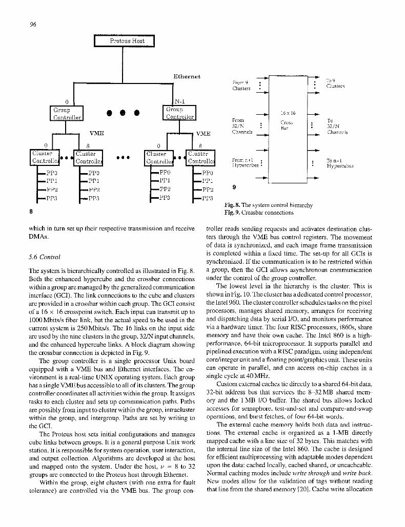
Proteus Host [
o
Group i Controller
I wE ~ 18
Cluster I Cluster ] Controllel' " ~ Controlle~
mPP0 - - P P 0 �9 -,PPI --,PPl
---PP2 --,PP2
---PP3 --PP3
O �9 �9
O 0 0
Etherne t
IN-1 Group ] Controller
7L] o 8
I Cluster k . JCluster I <ontronel lContronq
i n , PP0 -- .PP0 ,--PP1 - ,-PP1 ,,,-,PP2 -mpp2 m P P 3 ,--PP3
From 9 Clusters ,
From 3 2 / N ! Channels
16 x 16
Cross Bar
/
From n+l . | Hypercub L
9
Fig. 8. The system control hierarchy Fig. 9. Crossbar connections
To 9 Clusters
To 3 2 / N ChanneIs
To n + l Hype rcubes
which in turn set up their respective transmission and receive DMAs.
5.6 Control
The system is hierarchically controlled as illustrated in Fig. 8. Both the enhanced hypercube and the crossbar connections within a group are managed by the generalized communication interface (GCI). The link connections to the cube and clusters are provided in a crossbar within each group. The GCI consist of a 16 x 16 crosspoint switch. Each input can transmit up to 1000 Mbits/s fiber link, but the actual speed to be used in the current system is 250 Mbits/s. The 16 links on the input side are used by the nine clusters in the group, 32/N input channels, and the enhanced hypercube links. A block diagram showing the crossbar connection is depicted in Fig. 9.
The group controller is a single processor Unix board equipped with a VME bus and Ethernet interfaces. The en- vironment is a real-time UNIX operating system. Each group has a single VME bus accessible to all of its clusters. The group controller coordinates all activities within the group. It assigns tasks to each cluster and sets up communication paths. Paths are possibly from input to cluster within the group, intracluster within the group, and intergroup. Paths are set by writing to the GCI.
The Proteus host sets initial configurations and manages cube links between groups. It is a general purpose Unix work station. It is responsible for system operation, user interaction, and output collection. Algorithms are developed at the host and mapped onto the system. Under the host, u = 8 to 32 groups are connected to the Proteus host through Ethernet.
Within the group, eight clusters (with one extra for fault tolerance) are controlled via the VME bus. The group con-
troller reads sending requests and activates destination clus- ters through the VME bus control registers. The movement of data is synchronized, and each image frame transmission is completed within a fixed time. The set-up for all GCIs is synchronized. If the communication is to be restricted within a group, then the GCI allows asynchronous communication under the control of the group controller.
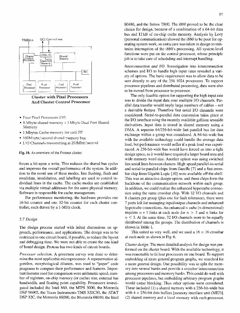
The lowest level in the hierarchy is the cluster. This is shown in Fig. 10. The cluster has a dedicated control processor, the Inte1960. The cluster controller schedules tasks on the pixel processors, manages shared memory, arranges for receiving and dispatching data by serial I/O, and monitors performance via a hardware timer. The four RISC processors, i860s, share memory and have their own cache. The Intel 860 is a high- performance, 64-bit microprocessor. It supports parallel and pipelined execution with a RISC paradigm, using independent core/integer unit and a floating point/graphics unit. These units can operate in parallel, and can access on-chip caches in a single cycle at 40 MHz.
Custom external caches tie directly to a shared 64-bit data, 32-bit address bus that services the 8-32MB shared mem- ory and the 1 MB I/O buffer. The shared bus allows locked accesses for semaphore, test-and-set and compare-and-swap operations, and burst fetches, of four 64-bit words.
The external cache memory holds both data and instruc- tions. The external cache is organized as a 1-MB directly mapped cache with a line size of 32 bytes. This matches with the internal line size of the Intel 860. The cache is designed for efficient multiprocessing with adaptable modes dependent upon the data: cached locally, cached shared, or uncacheable. Normal caching modes include write through and write back. New modes allow for the validation of tags without reading that line from the shared memory [20]. Cache write allocation
97
rMEbu s GCI Connections
Shared ?rocesso
P ..... 1 IProcessorl
Clus ter w i t h P i x e l P r o c e s s o r s And Clus ter Contro l P r o c e s s o r
�9 Four Pixel Processors (PP) �9 8 Mbyte shared memory + 1 Mbyte Dual Port Shared
Memory
�9 1 Mbytes Cache memory for each PP
�9 160Mbyte/second shared memory bus �9 I /O Channels transmitting at 250Mbit/second
Fig. 10. An overview of the Proteus cluster
forces a hit upon a write. This reduces the shared bus cycles and improves the overall performance of the system. In addi- tion to the novel use of these modes, line flushing, flush and invalidate, invalidation, and labelling are used to control in- dividual lines in the cache. The cache modes are established via multiple virtual addresses for the same physical memory. Software is responsible for cache management.
For performance monitoring, the hardware provides one 16-bit counter and one 32-bit counter for each cluster con- troller, each driven by a 1-MHz clock.
5. 7 Design
The design process started with initial discussions on ap- proach, performance, and applications. The design was to be restricted to one circuit board, if possible, to reduce the layout and debugging time. We were not able to create the one kind of board design. Proteus has two kinds of circuit boards.
Processor selection. A processor survey was done to deter- mine the most applicable microprocessor. A representative al- gorithm, morphological dilation, was used to "paper" code programs to compare their performance and features. Impor- tant features used for comparison were arithmetic speed, num- ber of registers, on-chip memory (or cache) size, external bus bandwidth, and floating point capability. Processors investi- gated included the Intel 860, the MIPS 3000, the Motorola DSP 96002, the Texas Instruments TMS 320C30, the AT&T DSP 32C, the Motorola 88000, the Motorola 68040, the Intel
80486, and the Inmos T800. The i860 proved to be the clear choice for design, because of a combination of a 64-bit data bus and 12 kB of on-chip cache memory. Analysis by Levy (personal communication) showed the i860 to be poor for op- erating system work, so extra care was taken in design to min- imize interruption of the i860's processing. All system-level functions were put on the control processor, whose principle job is to take care of scheduling and interrupt handling.
Interconnection and I/0. Investigation into interconnection schemes and I/O to handle high input rates revealed a vari- ety of options. The basic requirement was to allow data to be sent directly to any of the 256 1024 processors. To support processor pipelines and distributed processing, data were also to be moved from processor to processor.
The only feasible option for supporting the high input rate was to divide the input data over multiple I/O channels. Par- allel data transfer would imply large numbers of cables - not a desirable feature. Therefore fast serial I/O channels were considered. Serial-to-parallel data conversion takes place at the I/O interface using the recently available gallium arsenide derivatives. Input data is stored in shared memory using a DMA. A separate 64/256-bit-wide fast parallel bus for data exchange within a group was considered. A 64-bit-wide bus with the available technology could handle the average data load, but performance would suffer if a peak load was experi- enced. A 256-bit-wide bus would have forced us into a tight design space, as it would have required a larger board area and wide memory word size. Another option was using switched fast serial lines between clusters. High-speed parallel-to-serial and serial-to-parallel chips from Gazelle [7] and a fast cross- bar chip from Gigabit Logic [10] were available off the shelf. This was an attractive design option, and these chips form the backbone of the communication network within each gmup. In addition, we could realize the enhanced hypercube connec- tion using the same crossbar chip. With 32 I/O channels and 8 clusters per group (plus one for fault tolerance), there were 7 ports left for managing input/output channels and enhanced hypercube connections. An enhanced n-cube (n dimensional) requires n + 1 links at each node for n > 3 and n links for n _< 3. At the same time, 32 I/O channels were to be equally distributed among the groups. The distribution of channels is shown in Table 1.
This suited us very well, and we used a 16 x 16 crossbar at each node as shown in Fig. 6.
Cluster design. The most detailed analysis for design was per- formed on the cluster board. With the available technology, it was reasonable to fit four processors on one board. To support embedding of more general program graphs, we searched for a more general design. One possibility was to split the mem- ory into several banks and provide a crossbar interconnection among processors and memory banks. This could do well with processor pipelines, but embedding arbitrary program graphs would cause blocking. Thus other options were considered. These included (1) a shared memory with a 256-bit-wide bus with 4 x 256-bit data buffers [memory interface unit (MIU)], (2) shared memory and a local memory with each processor,
98
and (3) a shared memory with processor caches. In each case, it was possible to share the memory for I/O through DMA or provide separate buffering for I/O. The bus could be 64 or 256 bits wide. These alternatives were compared using Net- work II.5 simulations and then low-level hardware description language (HDL) simulations.
Several things were learned from the simulations. A large amount of conflict resulted whenever the input data was being transferred into shared memory. Because of this, closer atten- tion was paid to the I/O design on the board. With the use of an I/O buffer, the input and output data could be removed from the shared bus. Therefore, a dual port memory was added to manage the I/O. The MIU model suffered because the proces- sor could not cache all of its data in its on chip cache and more contention resulted. In addition, a 256-bit bus was thought to be an implementation risk. The local memory model suffered because no processing occurred while data was being trans- ferred to shared memory and because the local memory has a fixed size. However, local memory is advantageous when processing creates large results to be used again by the same processor. The cache solution computed while reading initial data did not fix the size of programs and data, and it allowed a 64-bit bus to achieve acceptable performance. However, de- pending on the algorithm, the bus could still be saturated.
Additional optimization of caching was investigated. When blocks of data are to be generated as a result of computation, reads are not necessary for caching. Block processing of data leads to the idea of allowing pages of the cache to be controlled in a local memory mode, so local data could be forced to stay off the shared memory bus. Through allocation, a section of the cache was to allow allocated writes. These writes would hit irrespectively of the address tag present in the cache. If valid data previously in the cache needed to be flushed, this would be done, before the write.
Further investigation showed that clever coding on the pro- cessor allowed results to be cached, which dramatically re- duced traffic on tile bus. Since the i860 allowed 64-bit trans- fers, using the bus for less than 64-bit transfers is inefficient. In particular, if the transfer happens to be a byte, which was the case for our first vision application, the performance loss is severe. Therefore, a scheme in which write data are cached and transferred to main memory in chunks of 64 bits yields much improved performance. Table 2 shows the results of this study. Three models were studied: (A) a statistical read/write model, (B) a deterministic read/write model, and (C) a statisti- cal read/write model that caches the writes. The same program runs on all four processors. It processes a 64-Kb image and creates a 64-Kb image in an optimistic 40 ms. In the first two models, A and B, the byte pixel writes go directly to the shared memory, so that all four processor writes may cause conflicts. Model C reduces write traffic by writing words of 8 pixels, which would be flushed from the on-chip cache.
One way to force a hit on writes was to modify cache tags, a feature available in the i860. However, that required extensive modification in program development. An alternative was to read result locations before writing. This happens naturally in many applications in which the computation is of the form
Table 1. Distribution of channels
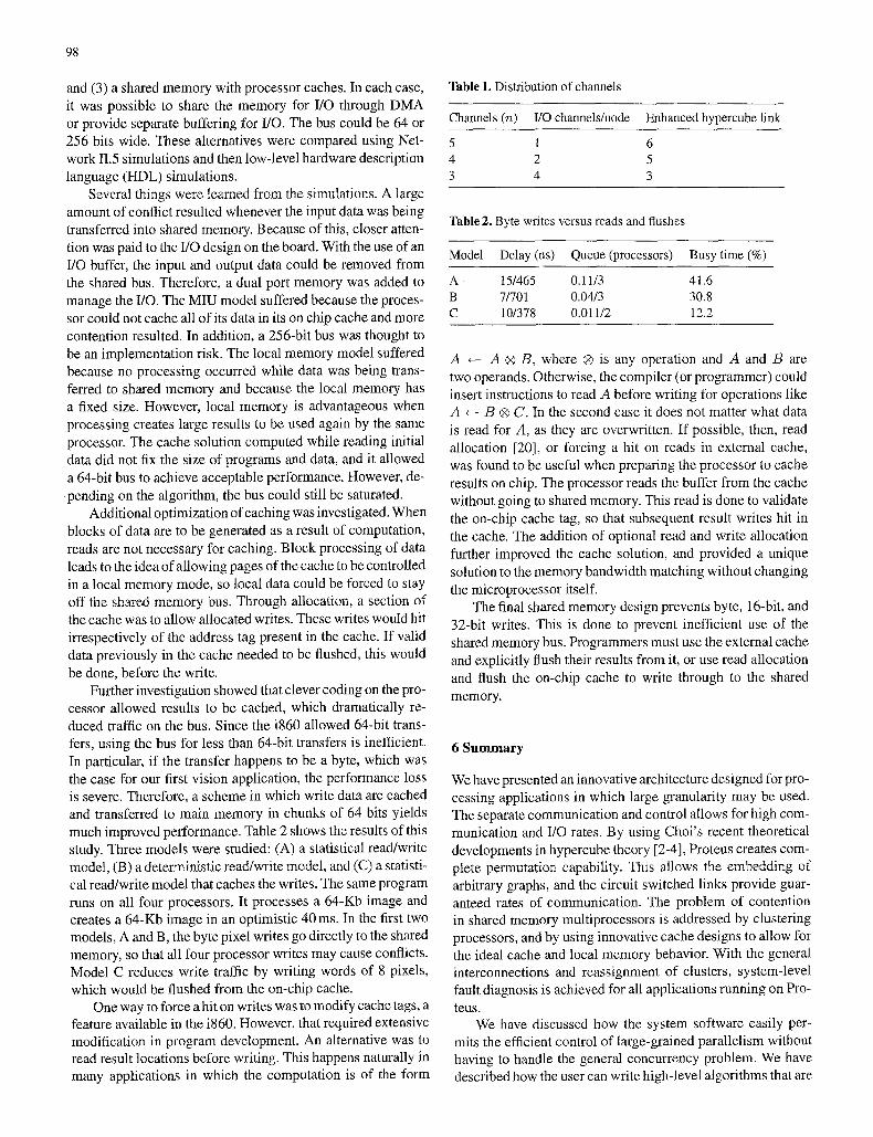
Channels (n) I/O channels/node Enhanced hypercube link
5 1 6 4 2 5 3 4 3
Table 2. Byte writes versus reads and flushes
Model Delay (ns) Queue (processors) Busy time (%)
A 15/465 0.11/3 41.6 B 7/701 0.04/3 30.8 C 10/378 0.011/2 12.2
A ~-- A | B, where | is any operation and A and /3 are two operands. Otherwise, the compiler (or programmer) could insert instructions to read A before writing for operations like A +- /3 | C. In the second case it does not matter what data is read for A, as they are overwritten. If possible, then, read allocation [20], or forcing a hit on reads in external cache, was found to be useful when preparing the processor to cache results on chip. The processor reads the buffer from the cache without going to shared memory. This read is done to validate the on-chip cache tag, so that subsequent result writes hit in the cache. The addition of optional read and write allocation further improved the cache solution, and provided a unique solution to the memory bandwidth matching without changing the microprocessor itself.
The final shared memory design prevents byte, 16-bit, and 32-bit writes. This is done to prevent inefficient use of the shared memory bus. Programmers must use the external cache and explicitly flush their results from it, or use read allocation and flush the on-chip cache to write through to the shared memory.
6 Summary
We have presented an innovative architecture designed for pro- cessing applications in which large granularity may be used. The separate communication and control allows for high com- munication and I/O rates. By using Choi's recent theoretical developments in hypercube theory [2-4], Proteus creates com- plete permutation capability. This allows the embedding of arbitrary graphs, and the circuit switched links provide guar- anteed rates of communication. The problem of contention in shared memory multiprocessors is addressed by clustering processors, and by using innovative cache designs to allow for the ideal cache and local memory behavior. With the general interconnections and reassignment of clusters, system-level fault diagnosis is achieved for all applications running on Pro- teus.
We have discussed how the system software easily per- mits the efficient control of large-grained parallelism without having to handle the general concurrency problem. We have described how the user can write high-level algorithms that are
99
efficiently mapped to the Proteus hardware by the INSIGHT translator. We have shown how the reconfigurable computation network can get its act together.
The Proteus system design is not an academic design. We have implemented it and are in the final system integration stages. Our first morphological [11] image processing appli- cation has been prototyped. Then we expected to expand the application software to include higher-level computer vision operations as part of the INSIGHT language. Unfortunately, Congress cancelled the program under which this project was funded, so further work was terminated.
References
1. Campbell ML (1985) Static allocation for a dataflow multiproces- sor. Proceedings of the 1985 International Conference on Parallel Processing, pp 511-517, St. Charles, I1l
2.Choi SB, Somani AK (1990) The generalized hypercube. Proceed- ings of the International Conference on Parallel Processing 90, pp 372-375
3. Choi SB, Somani AK (1993) Rearrangeable hypercube architec- ture for routing permutations. J Parallel Distributed Computing 19:125-130
4. Choi SB, Somani AK (1991) The generalized folding-cube net- work. Networks 21:267-294
5.Dongarra JJ, Duff IS (1989) Advanced architecture computers. Technical Memo No. 57, Argonne National Laboratory, Argonne, Ill
6. Duncan R (1990) A survey of parallel computer architectures. IEEE Computer 39:5-16
7. Gazelle Preliminary HOT ROD high speed serial link gallium ar- senide. GA 9011, GA 9012, Gazelle Microcircuits, Santa Clara, Calif
8. Geist GA, Heath MT, Peyton BW, Worley PH (1990) A user's guide to PICL: a portable instrumented communication library. ORNL/TM-11616, Oak Ridge National Laboratory, Oakridge, Tenn
9. Geist GA, Heath MT, Peyton BW, Worley PH (1990) A user's guide to PICL: a portable instrumented communication library, C Reference Manual. ORNL/TM- 11130 Oak Ridge National Lab- oratory, Oakridge, Tenn
i0. Gigabit Logic 16 x 16 Crosspoint switch 2.6Gbits/s data rate/1.8 ns reconfiguration time. 10G051 Gigabit Logic, San Jose, Calif
11. Haralick RM, Sternberg SR, Zhuang Y (1987) Image analysis using mathematical morphology. IEEE Trans Part Anal Machine Intell 9:532-550
12. Heath MT (1991) Visualizing the performance of programs. IEEE Software, vol 8, no 5, pp 29-39
13. Hsu JM, Banerjee P (1990) Performance measurement and trace driven simulation of parallel CAD and numeric applications on a hypercube multicomputer. Proceedings of the 17th Annual In- ternational Symposium on Computer Architecture 18:260-269
14. Hwang K, Dubois M, Pansk DK, Rar S, Shang S (1990) OMP: A RISC-based multiprocessor using orthogonal-access memo- ties and multiple spanning buses. International Conference on Supercomputing, Amsterdam, 7-22
15. Kruse B (1983) State-of-the-art systems for pictorial information processing. In: Faugeras OD (ed) Fundamentals in computer vi- sion. Cambridge University Press, Cambridge, pp 425--442
16. Olson CF (1990) Load balancing in dataflow multiprocessors, a project for EE 595. Technical Report, University of Washington, Seattle, Wa
17. Rice TA, Jamieson LH (1985) Parallel processing for computer vision. In: Levialdi S (ed) Integrated technology for parallel im- age processing. Academic Press, London, pp 57-78
18. Shapiro LG (1989) Programming parallel vision algorithms: a dataflow language approach. Int J Supercomput Appl 2:29--44
19. Shapiro LG, Haralick RM, Goulish M (1987) INSIGHT: a dataflow language for programming vision algorithms in a recon- figurable computational network. Int J Artif Intell Patt Recogn 1:335-350
20. Somani AK, Agarwal VK (1989) Distributed syndrome-decoding for regular interconnected structures. Proceedings of IEEE Fault Tolerant Computing System 19, Chicago, Ill, pp 70-77
21. Sternberg SR (1981) Parallel architectures for image processing. In: Onoe M, Preston K, Rosenfeld A (eds) Real-time/parallel computing. Plenum Press, New York, NY, pp 347-359
22. Wadge WW, Ashcroft EA (1984) LUCID: the dataflow program- ming language. Academic Press, London
23. Wittenbrink C, Somani AK (1993) Cache tiling for high perfor- mance morphological image processing
24. Wittenbrink C (1990) Directed data cache for high performance morphological image processing. Master's Thesis, Department of Electrical Engineering, University of Washington, Seattle, Wa
25. Yalamanchili S, Palem KV, Davis LS, Welch AJ, Agarwal JK (1985) Image processing architectures: a taxonomy and survey. In: Kanal LN, Rosenfeld A (eds) Progress in pattern recognition. Elsevier Science Publishers, North-Holland, Amsterdam, pp 1- 37
26. Zhuang X, Haralick RM (1986) Morphological structuring el- ement decomposition. Comput Vision Graph Image Processing 35:370-382
100
Robert M. Haralick received a BA degree in mathematics from the University of Kansas in 1964, a BS degree in electrical engineering in 1966, and an MS degree in electrical engineering in 1967. In 1969, after completing his PhD at the University at Kansas, he joined the faculty of the Electrical Engineering Department where he served as Professor from 1975 to 1978. In 1979 Dr. Haralick joined the Elec- trical Engineering Department at Virginia Polytechnic Institute and State University where he was a professor and Director of the spatial Data Analysis Laboratory. From 1984 to 1986 Dr. Haralick served as Vice President of Research at Machine Vision International, Ann Arbor, Michigan. Dr. Haralick now occupies the Boeing Clairmont Egtvedt Professorship in the Department of Electrical Engineering at the University of Washington. Professor Haralick is a fellow of IEEE for his contributions in computer vision and image processing. He served on the Editorial Board of IEEE Transactions on Pattern Analysis and Machine Intelligence. He is the computer vision area ed- itor for Communications of the ACM, and serves as Associate Editor for Computer Vision, Graphics, and Image Processing, and Pattern Recognition. Professor Haralick's recent work is in shape analysis and extraction using the techniques of mathematic morphology. He has developed the morphological sampling theorem that establishes a sound shape/size basis for the focus of attention mechanism that can process image data in multiresolution mode, thereby making some of the image feature extraction processes execute more efficiently.
Arun K. Somani received his B.E. (Honors) degree in Electronics Engineering from BMa Institute of Technology and Science, Pilani, India, in 1973, and M. Eng. and Ph.D. degrees in Electrical Engineer- ing from McGill University, Montreal, Canada, in 1983 and 1985, respectively. From 1974 to 1982 he worked as a scientist in the Sys- tem Group, Department of Electronics, Government of India, New Delhi. Currently he is an associate professor of electrical engineering and computer science and engineering at University of Washington, Seattle. Dr. Somani's research interests include computer architec- ture, fault tolerant computing, parallel computer system and algo- rithms, and computer interconnection networks. He is the architect of the Proteus Computer System, a large reconfigurable network of processors for image and vision processing applications designed and built at the University of Washington.
Craig M. Wittenbrink is a post doctoral researcher at the University of California, Santa Cruz, where he does research in environmental visualization. He received his B.S. in 1987 in electrical engineering and computer science from the University of Colorado, his M.S. in 1990 and his Ph.D. in 1993 in electrical engineering from the Univer- sity of Washington. He was a design engineer with Boeing Aerospace from 1987 to 1989 developing computer image generators.
Linda G. Shapiro was born in Chicago, Illinois, 1949. She received a B.S. degree in mathematics from the University of Illinois, Urbana, in 1970, and M.S. and Ph.D. degrees in computer science from the Uni- versity of Iowa, Iowa City, in 1972 and 1974, respectively. She was an
Assistant Professor for Computer Science at Kansas State Univer- sity, Manhattan, from 1974 to 1978 and was an Assistant Professor of Computer Science from 1979 to 1981 and Associate Professor of Computer Science from 1981 to 1984 at Virginia Polytechnic Insti- tute and State University, Blacksburg. She was Director of Intelligent Systems at Machine Vision International in Ann Arbor from 1984 to 1986. She is currently Professor of Computer Science and Engineer- ing and of Electrical Engineering at the University of Washington. Her research interests include computer vision, artificial intelligence, pattern recognition, robotics, and spatial database systems. She has coauthored two textbooks, one on data structures and one on com- puter and robot vision. Dr. Shapiro is a senior member of the IEEE Computer Society and a member of the Association for Computing Machinery, the Pattern Recognition Society, and the American Asso- ciation for Artificial Intelligence. She is past Editor of CVGIP: Image Understanding and is currently an editorial board member of IEEE Transactions on Pattern Analysis and Machine Intelligence and of Pattern Recognition.
Jenq-Neng Hwang received the BS and MS degrees, both from elec- trical engineering, from the National Taiwan University, Taipei, Tai- wan, in 1981 and 1983 separately. After two years of obligatory mili- tary services, he enrolled as a research assistant in 1985 at the Signal and Image Processing Institute, Dept. of Electrical Engineering, Uni- versity of Southern California, where he received his Ph.D. degree in December 1988. He was also a visiting student at Princeton Univer- sity, New Jersey, from 1987 to 1989. Since summer 1989, he has been with Department of Electrical Engineering of University of Washing- ton at Seattle as an Assistant Professor. His research interests include signal/image processing, statistical data analysis, computational neu- ral networks, parallel algorithm design, VLSI array architecture. Dr. Hwang served as the Secretary of the Neural Systems and Applica- tions Committee of the IEEE Circuits and Systems Society from 1989 to 1991, and is a member of Technical Committees in IEEE Signal Processing Society: VLSI Signal Processing and Neural Networks Signal Processing. Currently, he is also serving as an associate editor for IEEE Transactions on Signal Processing and IEEE Transactions on Neural Networks. Dr. Hwang is the conference program chair of 1994 IEEE Workshop on Neural Networks for Signal Processing to be held in Ermioni, Greece.
Yung-Hsi Yao is a Ph.D. student in Electrical Engineering at the Uni- versity of Washington. He received his B.S. in Electronic Engineering from National Chiao-Tung University (Hsin-Chu, Taiwan, ROC), his M.S. in Electrical Engineering from University of Florida. He is the main designer and implementor of the software system of the Proteus, a multiple-instruction, multiple-data machine for image processing and computer vision. His current research interest includes parallel computer system, parallel algorithms, computer vision, artificial in- telligence, pattern recognition, and robotics.