Embed Size (px)
Citation preview

PSpice™ based Examples
[Copyright 2003, Adapted with permission from “Power Electronics Modeling Simplified using PSpice™ (Release 9)”: http://www.mnpere.com]

TOC-1
TABLE OF CONTENTS
Section 1 Line-Frequency Diode Rectifiers
1. 1-phase Diode Bridge Rectifiers (DBRECT1) 2. 3-phase Diode Bridge Rectifiers (DBRECT3)
Section 2 Line-Frequency Phase-Controlled Converters
3. 1-phase Thyristor Rectifier Bridge (THYRECT1) 4. 1-phase Thyristor Inverters (THYINV1) 5. 3-phase Thyristor Rectifier Bridge (THYRECT3) 6. 3-phase Thyristor Inverter (THYINV3)
Section 3 DC-to-DC Switch-Mode Converters
7. Step-down (Buck) dc-dc Converter (BUCKCONV) 8. Step-up (Boost) dc-dc Converter (BOOST) 9. Step-down/up (Buck-Boost) dc-dc Converter (BUCK-BOOST) 10. Full-bridge, bipolar-voltage-switching dc-dc Converter (FBBSDCDC) 11. Full-bridge, unipolar-voltage-switching dc-dc Converter (FBUSDCDC)
Section 4 Switch-Mode DC-to-Sinusoidal Inverters 12. PWM, bipolar-voltage-switching, 1-phase (1PHBSINV) 13. PWM, unipolar-voltage-switching, 1-phase (1PHUSINV) 14. Square-Wave, 1-phase (1PHSQINV) 15. Voltage-Cancellation Control, 1-phase (1PHVCINV) 16. PWM Inverter, 3-phase (PWMINV3) 17. Square-Wave Inverter, 3-phase (SQINV3)
Section 5 Soft-Switching Converters: Zero Voltage/Current Switching
18. Series-Loaded Resonant dc-dc Converters Operating Above the Resonant frequency (SLRCM2) 19. Parallel-Loaded Resonant dc-dc Converter Operating Above the Resonant Frequency (PLRCM2) 20. Current-Source, Parallel-Resonant Inverters for Induction Heating (CSINV) 21. Zero-Current Switching, Quasi-Resonant Buck Converter (ZCSCONV) 22. Zero-Voltage Switching, Clamped-Voltage (Resonant Transition) Converter (ZVSCV)
Section 6 Switch-Mode DC Power Supplies with Isolation
23. Flyback Converters (FLYBACK) 24. Forward Converters (FORWARD) 25. Forward Converter: Voltage-Mode Controlled (FOR_CNTL)
Section 7 DC-Motor Drives
26. Ripple in the Armature Current (DC_MOTOR)
Section 8 Semiconductor Devices
27. Power MOSFET switching characteristics (MOSFET)
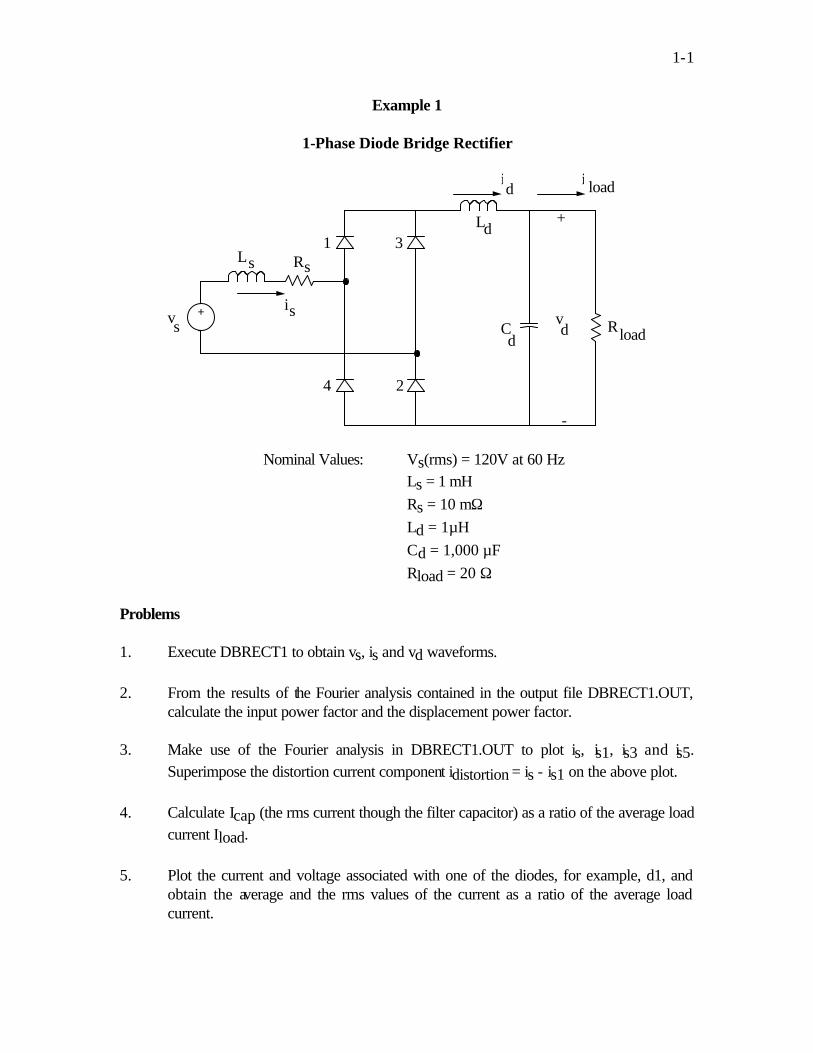
1-1
Example 1
1-Phase Diode Bridge Rectifier
+-
vs
1 3
4 2
i loadid
Cd
Rload
+
-
vd
Ls Rs
is
Ld
Nominal Values: Vs(rms) = 120V at 60 Hz Ls = 1 mH Rs = 10 mΩ Ld = 1µH Cd = 1,000 µF Rload = 20 Ω
Problems 1. Execute DBRECT1 to obtain vs, is and vd waveforms. 2. From the results of the Fourier analysis contained in the output file DBRECT1.OUT,
calculate the input power factor and the displacement power factor. 3. Make use of the Fourier analysis in DBRECT1.OUT to plot is, is1, is3 and is5.
Superimpose the distortion current component idistortion = is - is1 on the above plot. 4. Calculate Icap (the rms current though the filter capacitor) as a ratio of the average load
current Iload. 5. Plot the current and voltage associated with one of the diodes, for example, d1, and
obtain the average and the rms values of the current as a ratio of the average load current.

1-2
6. Vary Ls as a parameter to investigate its influence on the input displacement power factor, the input power factor, %THD, and the peak-peak ripple in the dc voltage vd.
7. Vary the filter capacitor Cd to investigate its influence on the percentage ripple in vd,
input displacement power factor and %THD. Plot the percentage ∆Vd (peak-to-peak)/Vd(average) as a function of Cd.
8. Vary the load power to investigate its influence on the average dc voltage. 9. In the nominal circuit input file, remove the limit on the maximum time step during the
simulation and observe its influence on the circuit waveforms. 10. Obtain the vs, is and vd waveforms during the startup transient when the filter capacitor
is initially not charged. Obtain the peak inrush current as a ratio of the peak current in steady state. Vary the switching instant by simply varying the phase angle θ of the source vs.
11. Replace the dc side of the diode bridge by a current source Id = 10 A, corresponding
to a very large Ld. Make Ls almost equal to zero. Obtain Vd(average). 12. Make Ls = 3 mH in Problem 10 and obtain Vd(average), displacement power factor,
power factor, %THD, and the current commutation interval.
Reference: Section 5-3-4, pages 95 - 99. PSpice Schematic: DBRECT1 [Copyright 2003, Adapted with permission from “Power Electronics Modeling Simplified using PSpice™ (Release 9)”: http://www.mnpere.com]
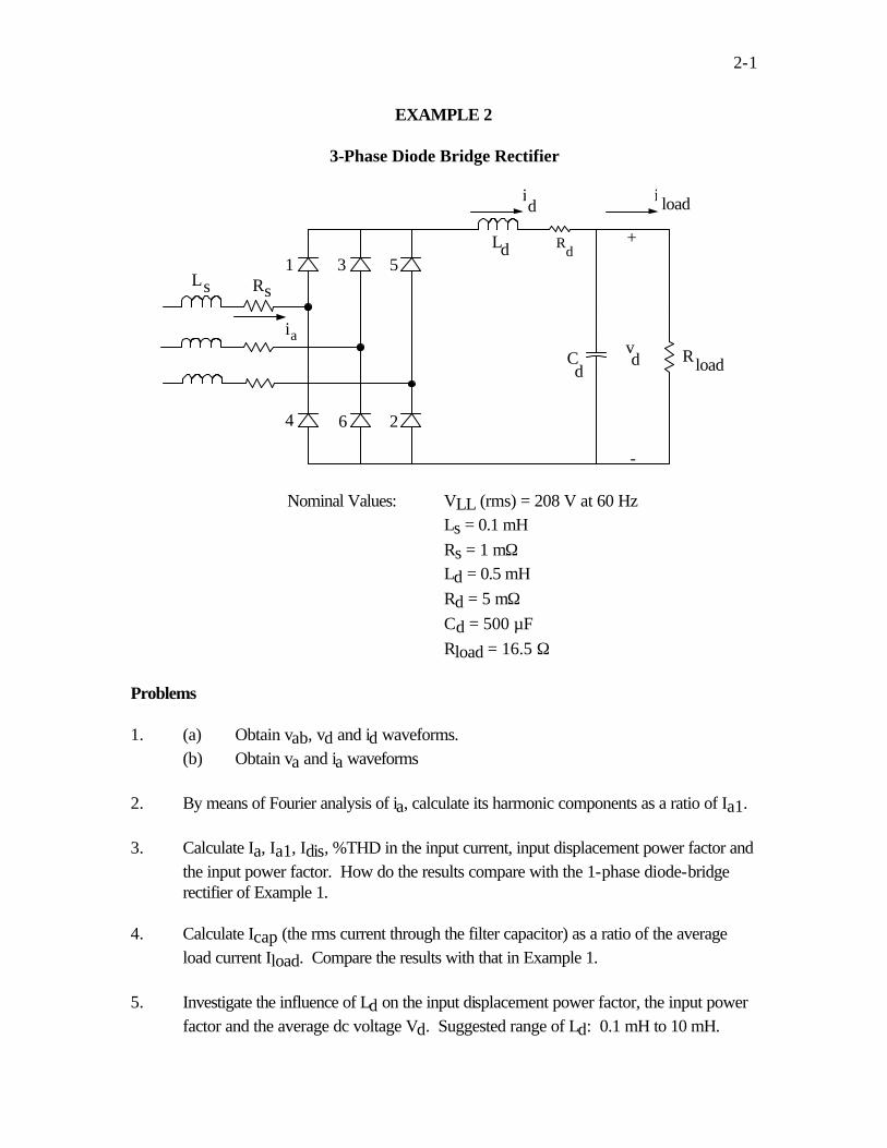
2-1
EXAMPLE 2
3-Phase Diode Bridge Rectifier
1 3
4
i loadid
Cd
Rload
+
-
vd
Ls Rs
i
Ld
a
5
6 2
Rd
Nominal Values: VLL (rms) = 208 V at 60 Hz Ls = 0.1 mH Rs = 1 mΩ Ld = 0.5 mH Rd = 5 mΩ Cd = 500 µF Rload = 16.5 Ω
Problems 1. (a) Obtain vab, vd and id waveforms.
(b) Obtain va and ia waveforms 2. By means of Fourier analysis of ia, calculate its harmonic components as a ratio of Ia1. 3. Calculate Ia, Ia1, Idis, %THD in the input current, input displacement power factor and
the input power factor. How do the results compare with the 1-phase diode-bridge rectifier of Example 1.
4. Calculate Icap (the rms current through the filter capacitor) as a ratio of the average
load current Iload. Compare the results with that in Example 1. 5. Investigate the influence of Ld on the input displacement power factor, the input power
factor and the average dc voltage Vd. Suggested range of Ld: 0.1 mH to 10 mH.

2-2
6. Investigate the influence of Cd on the percent ripple in vd. Plot the percentage ∆Vd
(peak-to-peak)/Vd(average) as a function of Cd. Suggested range of Cd: 100 µF and 2,000 µF.
7. Investigate the influence of Cd on the input displacement power factor and the input
power factor. Suggested range of Cd: 100 µF to 2,000 µF. 8. Plot the average dc voltage as a function of load. Suggested range of Rload: 50 Ω to 8
Ω. Reference: Section 5-6, pages 103 112. PSpice Schematic: Dbrect3 [Copyright 2003, Adapted with permission from “Power Electronics Modeling Simplified using PSpice™ (Release 9)”: http://www.mnpere.com]

3-1
EXAMPLE 3
1-Phase Thyristor Rectifier Bridge
+-
vs
1 3
4 2
id
R load
+
-
vd
i s
Ld
Ls1 Ls2
+
_
vm
Nominal values: Vs(rms) = 120 V at 60 Hz Ls1 = 0.2 mH Ls2 = 1.0 mH Ld = 20 mH Rload = 5 Ω delay angle α = 45° Problems 1. (a) Obtain vs, vd and id waveforms. (b) Obtain vs and is waveforms. (c) Obtain vm and is waveforms. 2. From the plots, obtain the commutation interval u and the dc-side current at the start of
the commutation. 3. By means of Fourier analysis of is, calculate its harmonic components as a ratio of Is1. 4. Calculate Is, %THD in the input current, the input displacement power factor and the
input power factor. 5. At the point of common coupling, obtain the following from the voltage vm waveform: (a) Line-notch depth ρ(%)

3-2
(b) Line-notch area and, (c) voltage %THD. 6. Obtain the average dc voltage Vd. Verify that
Vd = 0.9 Vs cosα - 2ωLs
π Id.
where first use the average value of id for Id and then its value at the start of the commutation interval as calculated in Problem 2.
Reference: Section 6-3, pages 126 - 134. PSpice Schematic: Thyrect1 [Copyright 2003, Adapted with permission from “Power Electronics Modeling Simplified using PSpice™ (Release 9)”: http://www.mnpere.com]

4-1
EXAMPLE 4
1-Phase Thyristor Inverter
+-
vs
1 3
4 2
id
+
-
vd
i s
Ld
Ls1 Ls2
+
_
vm +-
E
Nominal Values: Vs(rms) = 120 V at 60 Hz Ls1 = 0.2 mH Ls2 = 1.0 mH Ld = 20 mH E = 88 V (dc) delay angle α = 135° Problems 1. (a) Obtain vs, vd and id waveforms using Thyinv1. (b) Obtain vs and is waveforms. 2. Calculate Is, %THD in the input current, the input displacement power factor and the
input power factor. 3. Study the startup of inverter operation. Increase the delay angle to a value close to
180° (for example, 150°) and look at the vs, vd and id waveforms. Repeat the above procedure by reducing α slowly to its nominal value of 135°. Plot the average dc current Id versus α.
Reference: Section 6-3-4, pages 135 - 138. PSpice Schematic: Thyinv1 [Copyright 2003, Adapted with permission from “Power Electronics Modeling Simplified using PSpice™ (Release 9)”: http://www.mnpere.com]

5-1 EXAMPLE 5
3-Phase Thyristor Rectifier Bridge
1 3
4
id
Rload
+
-
vd
i
Ld
a
5
6 2
a
b
c
point of common coupling
Ls1 Ls2
Nominal Values: VLL(rms) = 208 V at 60 Hz Ls1 = 0.2 mH Ls2 = 1.0 mH Ld = 16 mH Rload = 8 Ω delay angle = 45° Problems 1. (a) Obtain va, vd and id waveforms using Thyrect3.
(b) Obtain va and ia waveforms. (c) Obtain (va)pcc, (vab)pcc and ia waveforms.
2. From the plots, obtain the commutation interval u and id at the start of the commutation.
Verify the following commutation equation:
cos(α+u) = cos α - 2ωLs2 VLL
Id
where Ls = Ls1 + Ls2. For Id, use the average value of id or its value at the start of the
commutation. 3. By means of Fourier analysis of is, calculate its harmonic components as a ratio of Is1. 4. Calculate Is, %THD in the input current, the input displacement power factor and the
input power factor.

5-2 5. Verify the following equation:
Displacement power factor ~ cos(α + u2 ) ~
cosα + cos(α+u)2
6. At the point of common coupling, obtain the following from the voltage vpcc waveform:
(a) Line-notch depth ρ(%) (b) Line-notch area and, (c) voltage THD%
7. Obtain the average dc voltage Vd. Verify that
Vd = 1.35 VLL cos α - 3ωLs
π Id.
For Id, use the average value of id or its value at the start of the commutation. Reference: Section 6-4, pages 138 - 148. PSpice Schematic: Thyrect3 [Copyright 2003, Adapted with permission from “Power Electronics Modeling Simplified using PSpice™ (Release 9)”: http://www.mnpere.com]
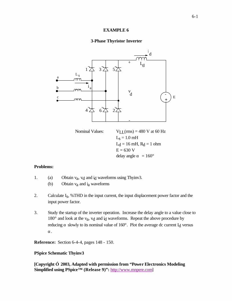
6-1
EXAMPLE 6
3-Phase Thyristor Inverter
1 3
4
id
+
-
vd
i
Ld
a
5
6 2
a
b
c+-
E
L s
Nominal Values: VLL(rms) = 480 V at 60 Hz Ls = 1.0 mH Ld = 16 mH, Rd = 1 ohm E = 630 V delay angle α = 160° Problems: 1. (a) Obtain va, vd and id waveforms using Thyinv3.
(b) Obtain va and ia waveforms 2. Calculate Is, %THD in the input current, the input displacement power factor and the
input power factor. 3. Study the startup of the inverter operation. Increase the delay angle to a value close to
180° and look at the va, vd and id waveforms. Repeat the above procedure by reducing α slowly to its nominal value of 160°. Plot the average dc current Id versus α.
Reference: Section 6-4-4, pages 148 - 150. PSpice Schematic Thyinv3 [Copyright 2003, Adapted with permission from “Power Electronics Modeling Simplified using PSpice™ (Release 9)”: http://www.mnpere.com]
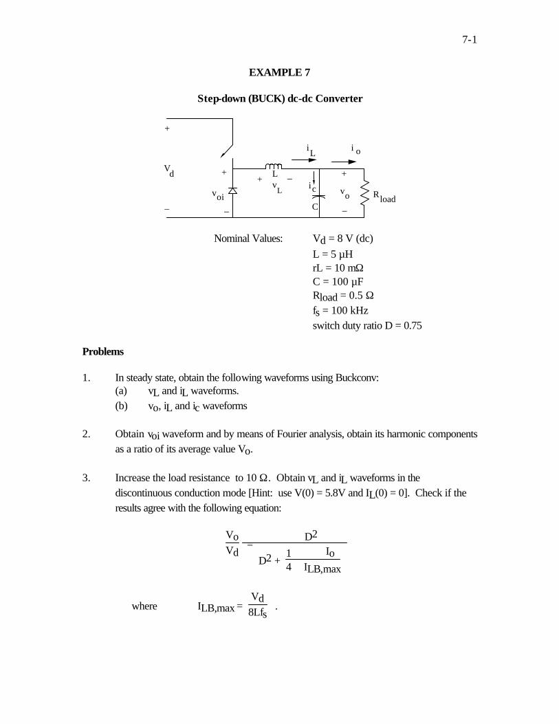
7-1
EXAMPLE 7
Step-down (BUCK) dc-dc Converter
+
_
L
C
+
_Rload
i i oL
+ _v
L
Vd
voic
+
_
voi
Nominal Values: Vd = 8 V (dc) L = 5 µH rL = 10 mΩ C = 100 µF Rload = 0.5 Ω fs = 100 kHz switch duty ratio D = 0.75 Problems 1. In steady state, obtain the following waveforms using Buckconv:
(a) vL and iL waveforms. (b) vo, iL and ic waveforms
2. Obtain voi waveform and by means of Fourier analysis, obtain its harmonic components
as a ratio of its average value Vo. 3. Increase the load resistance to 10 Ω. Obtain vL and iL waveforms in the
discontinuous conduction mode [Hint: use V(0) = 5.8V and IL(0) = 0]. Check if the results agree with the following equation:
VoVd
= D2
D2 + 14
Io
ILB,max
where ILB,max = Vd8Lfs
.

7-2
4. Obtain the peak-to-peak ripple in the output voltage and check to see if the results agree with the analytical calculations.
5. Calculate the rms value of the current through the output capacitor as a ratio of the
average load current Io. 6. Calculate the peak-to-peak ripple in the output voltage in the presence of the output
capacitor Equivalent Series Resistance (ESR) [Suggested ESR = 100 mΩ]. Plot the ripple across C, ESR and the total ripple in vo.
Reference: Section 7-3, pages 164 - 168. PSpice Schematic: Buckconv [Copyright 2003, Adapted with permission from “Power Electronics Modeling Simplified using PSpice™ (Release 9)”: http://www.mnpere.com]

8-1 EXAMPLE 8
Step-Up (Boost) dc-dc Converter
+
_
L
C
+
_Rload
i
i o
L
+ _v
LVd
voic
iD
Nominal Values: Vd = 9 V L = 10 µH rL = 10 mΩ C = 50 µF Rload = 5 Ω fs = 100 kHz switch duty ratio D = 0.625 Problems 1. In steady state obtain the following waveforms using Boost:
(a) vL and iL waveforms (b) vo, iD and ic waveforms
2. Obtain iD waveform and by means of Fourier analysis, obtain its harmonic components as a ratio of its average value Io.
3. Increase the load resistance to 50 Ω. Obtain vL and iL waveforms in the discontinuous conduction mode [Hint: use Vo(0) = 28 V and IL(0) = 0]. Check if the results agree with the analytical calculations.
4. After 10 ms, change the load resistance as a step from its nominal value of 5 Ω to 50 Ω. Obtain vL, iL and vo waveforms as they reach their new steady state values.
5. Obtain the peak-to-peak ripple in the output voltage and check to see if the results agree with the analytical calculations.
6. Calculate the rms value of the current through the output capacitor as a ratio of the average load current Io.
Reference: Section 7-4, pages 172 - 178.
PSpice Schematic: Boost [Copyright 2003, Adapted with permission from “Power Electronics Modeling Simplified using PSpice™ (Release 9)”: http://www.mnpere.com]
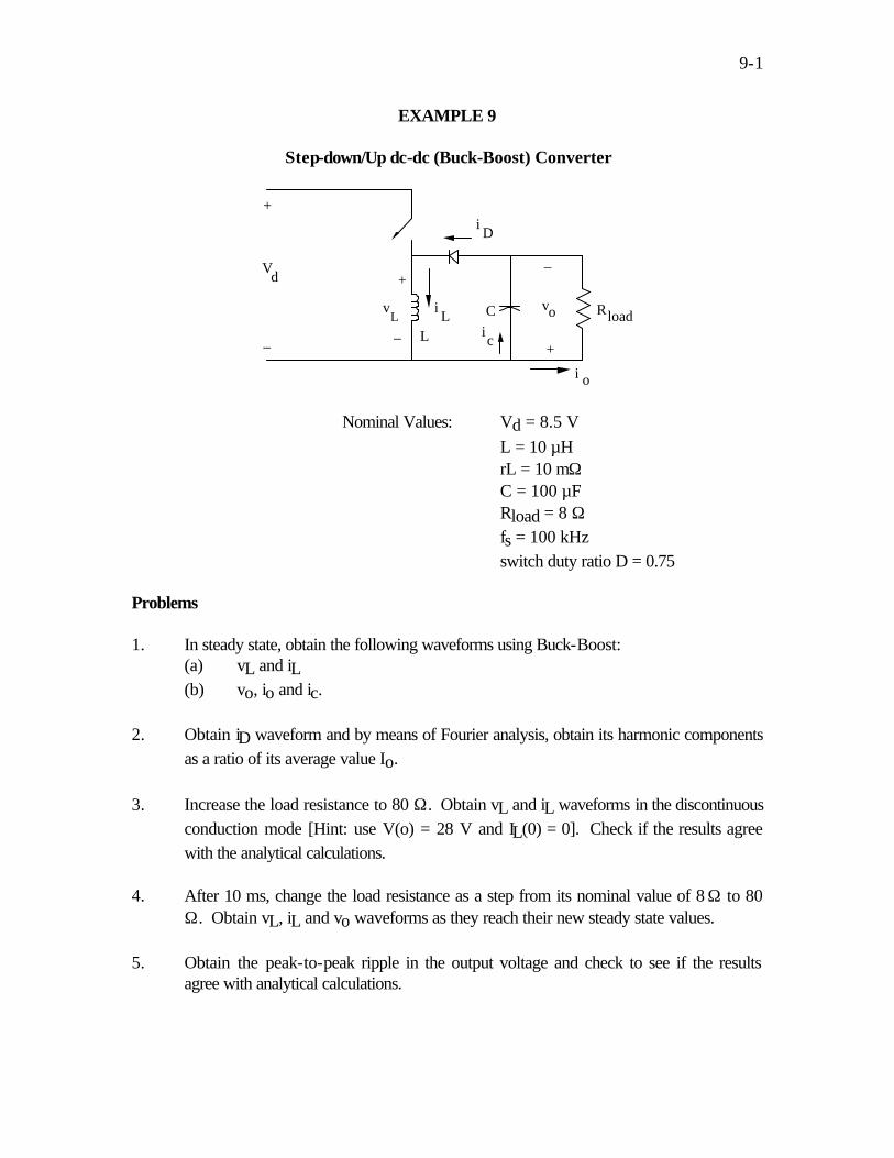
9-1
EXAMPLE 9
Step-down/Up dc-dc (Buck-Boost) Converter
+
_ L
C
+
_
Rload
i o
i L
+
_
vL
Vd
vo
i D
ic
Nominal Values: Vd = 8.5 V L = 10 µH rL = 10 mΩ C = 100 µF Rload = 8 Ω fs = 100 kHz switch duty ratio D = 0.75 Problems 1. In steady state, obtain the following waveforms using Buck-Boost:
(a) vL and iL (b) vo, io and ic.
2. Obtain iD waveform and by means of Fourier analysis, obtain its harmonic components
as a ratio of its average value Io. 3. Increase the load resistance to 80 Ω. Obtain vL and iL waveforms in the discontinuous
conduction mode [Hint: use V(o) = 28 V and IL(0) = 0]. Check if the results agree with the analytical calculations.
4. After 10 ms, change the load resistance as a step from its nominal value of 8 Ω to 80
Ω. Obtain vL, iL and vo waveforms as they reach their new steady state values. 5. Obtain the peak-to-peak ripple in the output voltage and check to see if the results
agree with analytical calculations.

9-2
6. Calculate the rms value of the current through the output capacitor as a ratio of the average load current Io.
Reference: Section 7-5, pages 178 - 184. PSpice Schematic: Buck-Boost [Copyright 2003, Adapted with permission from “Power Electronics Modeling Simplified using PSpice™ (Release 9)”: http://www.mnpere.com]
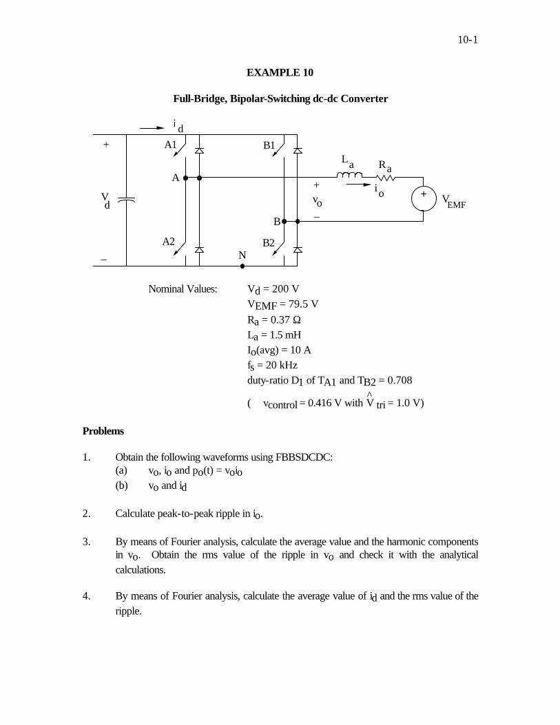
10-1
EXAMPLE 10
Full-Bridge, Bipolar-Switching dc-dc Converter
+-
+
_
Vd
A
B
N
La Ra
VEMF
i
A1 B1
A2 B2
+
_vo
o
i d
Nominal Values: Vd = 200 V VEMF = 79.5 V Ra = 0.37 Ω La = 1.5 mH Io(avg) = 10 A fs = 20 kHz duty-ratio D1 of TA1 and TB2 = 0.708
(∴ vcontrol = 0.416 V with ^V tri = 1.0 V)
Problems 1. Obtain the following waveforms using FBBSDCDC:
(a) vo, io and po(t) = voio (b) vo and id
2. Calculate peak-to-peak ripple in io. 3. By means of Fourier analysis, calculate the average value and the harmonic components
in vo. Obtain the rms value of the ripple in vo and check it with the analytical calculations.
4. By means of Fourier analysis, calculate the average value of id and the rms value of the
ripple.

10-2
5. With VEMF = 0 and Ia(avg) = 0, Vo(avg) = 0 V. Therefore, Vcontrol = 0. Calculate the following [Hint: use Io(0) = -1.67A]: (a) vo, io and po(t) waveforms. (b) peak-to-peak ripple in io. Compare it with its analytical value, and that in
Problem 2. (c) In part (a), label the intervals during which various devices are conducting.
6. In the regenerative mode, the power flows from the load to the dc-bus at Vd. Let VEMF= 79.5V, Ia(avg) = 10A in the reverse direction, and Vo(avg) = 79.5 - 0.37x10 = 75.8V. Therefore,
Vcontrol = 75.8200 x 1.0 = 0.379.
Calculate parts (a) through (c) of Problem 5 [Hint: use Io(0) = -11.67 A]. Reference: Section 7-7-1, pages 190 - 192. PSpice Schematic: FBBSDCDC [Copyright 2003, Adapted with permission from “Power Electronics Modeling Simplified using PSpice™ (Release 9)”: http://www.mnpere.com]

11-1
EXAMPLE 11
Full-Bridge, Unipolar Switching dc-dc Converter
+-
+
_
Vd
A
B
N
La Ra
VEMF
i
A1 B1
A2 B2
+
_vo
o
i d
Nominal Values: Same as that in Example 10 except for unipolar-voltage switchings. Problems 1. Obtain the plot of vA, vB and vo using FBUSDCDC. 2. Obtain the plot of vo and io 3. Obtain the peak-peak ripple in io. Check it with its analytical value and compare it with
Problem 2 of Example 10. 4. Obtain the rms value of the ripple in vo. Check it with its analytical value and compare
it with Problem 3 of Example 10. Reference: Section 7-7-2, pages 192 - 194. PSpice Schematic: FBUSDCDC [Copyright 2003, Adapted with permission from “Power Electronics Modeling Simplified using PSpice™ (Release 9)”: http://www.mnpere.com]
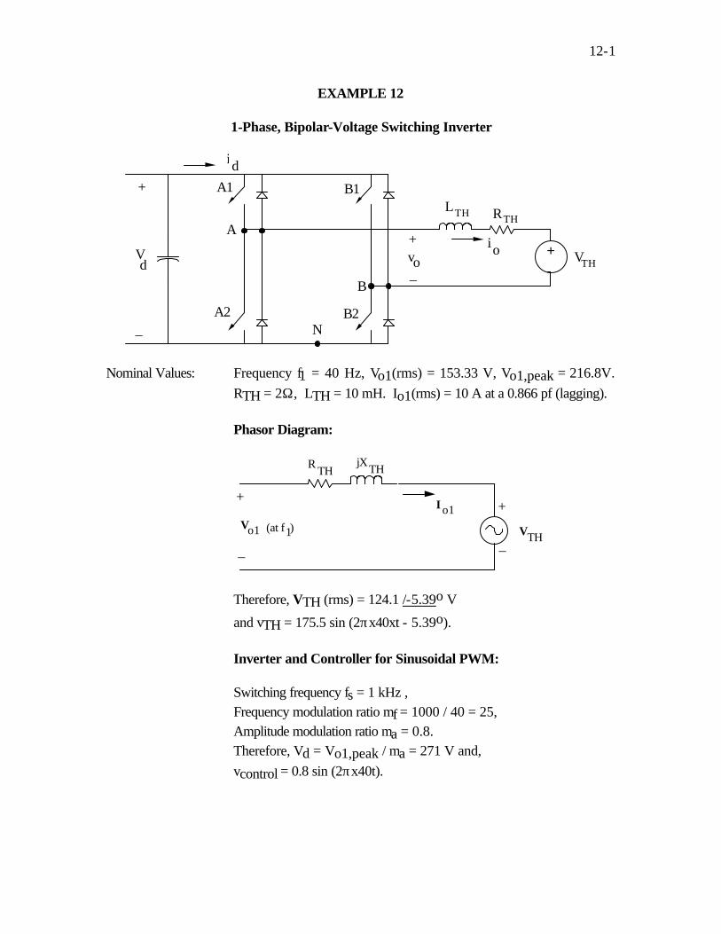
12-1
EXAMPLE 12
1-Phase, Bipolar-Voltage Switching Inverter
+-
+
_
Vd
A
B
N
L R
Vi
A1 B1
A2 B2
+
_vo
o
TH TH
TH
id
Nominal Values: Frequency f1 = 40 Hz, Vo1(rms) = 153.33 V, Vo1,peak = 216.8V. RTH = 2Ω, LTH = 10 mH. Io1(rms) = 10 A at a 0.866 pf (lagging). Phasor Diagram:
+
_
+
_
R THjXTH
I o1Vo1 (at f )1 VTH
Therefore, VTH (rms) = 124.1 /-5.39o V
and vTH = 175.5 sin (2πx40xt - 5.39o).
Inverter and Controller for Sinusoidal PWM: Switching frequency fs = 1 kHz , Frequency modulation ratio mf = 1000 / 40 = 25, Amplitude modulation ratio ma = 0.8. Therefore, Vd = Vo1,peak / ma = 271 V and, vcontrol = 0.8 sin (2πx40t).

12-2
Problems 1. Obtain the following waveforms using 1Phbsinv:
(a) vo and io. (b) vo and id. (c) vo, io and po.
2. Obtain v01 by means of Fourier analysis of the vo waveform. Compare v01 with its
precalculated nominal value. 3. Using the results of Problem 2, obtain the ripple component vripple waveform in the
output voltage. 4. Obtain i01 by means of Fourier analysis of the io waveform. Compare i01 with its
precalculated nominal value. 5. Using the results of Problem 4, obtain the ripple component iripple in the output current. 6. Obtain Id(avg) and id2 (the component at the 2nd harmonic frequency) by means of the
Fourier analysis of the id waveform. Compare them with their precalculated nominal values.
7. Using the results of Problem 6, obtain the high frequency ripple component id,ripple in
the input dc current. Calculate its rms value. Reference: Section 8-3-2-1, pages 212 - 215. PSpice Schematic: 1Phbsinv
Based on Io1(rms) = 10 /-30o A, the initial value Io(o) = -7 A.
[Copyright 2003, Adapted with permission from “Power Electronics Modeling Simplified using PSpice™ (Release 9)”: http://www.mnpere.com]

13-1
EXAMPLE 13
1-Phase, Unipolar-voltage Switching Inverter
+-
+
_
Vd
A
B
N
L R
Vi
A1 B1
A2 B2
+
_vo
o
TH TH
TH
id
Nominal Values: Similar to Example 12. Problems 1. Obtain the following waveforms using 1Phusinv:
(a) vo and io. (b) vo and id. (c) vo, io and po.
2. Obtain v01 by means of Fourier analysis of the vo waveform. Compare v01 with its
precalculated nominal value. 3. Using the results of Problem 2, obtain the ripple component vripple waveform in the
output voltage. Compare the peak-to-peak ripple to that in the bipolar-voltage switching inverter.
4. Obtain i01 by means of Fourier analysis of the io waveform. Compare i01 with its
precalculated nominal value. 5. Using the results of Problem 4, obtain the ripple component iripple in the output current.
Compare the peak-to-peak ripple to that in the bipolar-voltage switching inverter. 6. Obtain Id(avg) and id2 (the component at the 2nd harmonic frequency) by means of the
Fourier analysis of the id waveform. Compare them with their precalculated nominal values.

13-2
7. Using the results of Problem 6, obtain the high frequency ripple component id,ripple in the input dc current. Calculate its rms value. Compare the rms value of the dc-side current ripple to that in the bipolar-voltage switching inverter.
Reference: Section 8-3-2-2, pages 215 - 218. PSpice Schematic: 1Phusinv
Based on Io1(rms) = 10 /-30o A, the initial value Io(o) = -7 A. Controller:
The same controller PWM_TRI, as in Example 12 is used. The difference is that the switches in the converter-leg A depend on the control voltage vcontrol, whereas the switches in the converter-leg B depend on (- vcontrol).
[Copyright 2003, Adapted with permission from “Power Electronics Modeling Simplified using PSpice™ (Release 9)”: http://www.mnpere.com]

14-1 EXAMPLE 14
1-Phase, Square-Wave Inverter
+-
+
_
Vd
A
B
N
L R
Vi
A1 B1
A2 B2
+
_vo
o
TH TH
TH
id
Nominal Values: Same as in Example 12 except,
Vd = π4 V01,peak = 216.8
π4 = 170.27 V
Problems
Similar to Example 12 but compare the results with both Examples 12 and 13. Also, obtain the lower order harmonics in vo as a ratio of Vo1.
Reference: Section 8-3-2-3, page 218. PSpice Schematic: 1Phsqinv
Based on Io1(rms) = 10 /-30o A, the initial value Io(o) = -7 A. Controller:
Switches (A1, B2) and (B1, A2) form two switch pairs, each of which is gated on for alternate half periods.
[[Copyright 2003, Adapted with permission from “Power Electronics Modeling Simplified using PSpice™ (Release 9)”: http://www.mnpere.com]

15-1
EXAMPLE 15
1-Phase, Voltage-Cancellation Inverter
+-
+
_
Vd
A
B
N
L R
Vi
A1 B1
A2 B2
+
_vo
o
TH TH
TH
id
Nominal values: Same as in Example 14.
For Vd = 271 V and V 01 = 216.8V, at h = 1
216.8 = 4π 271 sin β
∴ β = 38.9° and α = 180−2β = 102.2°
0α=51.1
2
Problems Same as in Example 14. Reference: Section 8-3-2-4, pages 218 - 219. See the definitions of α and β . PSpice Schematic: 1Phvcinv
Based on Io1(rms) = 10 /-30o A, the initial value Io(o) = -7 A.

15-2
Controller:
0
0
0
0
180 o
180 o
360
360
o
o
A1 A2
B2 B1
[Copyright 2003, Adapted with permission from “Power Electronics Modeling Simplified using PSpice™ (Release 9)”: http://www.mnpere.com]

16-1 EXAMPLE 16
Three-Phase PWM Inverter
+
_
Vd
A
B
N
Vi
A1 B1
A2 B2
LTH RTH
TH
id
C
C1
C1
, AA
n
Nominal Values: Load: A 230 V, 60 Hz, 3-phase motor is operating at a frequency f1
= 47.619 Hz. Therefore,
VrmsLL1
= 47.619
60 x 230 = 182.54 V.
VrmsAn1
= V
rmsLL1
3 = 105.39 V = 105.39/0°.
IrmsA1
= 10 A at a lagging power factor of 0.866 = 10 /-30° A. Rs =
2Ω , Ls = 10 mH,
∴ Xs = 2πx47.619x10x10-3 = 3Ω. Phasor Diagram:
+
_
+
_
R THjXTH
I
VAn (at f )1 VTH , A
A1
11
∴ (VTH,A)1 = 74.76 /-12.36° V (rms) Inverter and Sinusoidal PWM Controller: Switching frequency fs = 1 kHz. Amplitude modulation ratio ma = 0.95 .
∴ Vd = V
rmsLL1
0.612 ma = 313.97 V. With
^V tri = 1.0 V

16-2 vcontrol,A = 0.95 cos (2πf1t - 90°) V.
Problems 1. Obtain the following waveforms using :
(a) vAN and iA. (b) van and iA. (c) vAN and id.
2. Obtain vAn1
by means of Fourier analysis of the vAn waveform. Compare vAn1 with
its precalculated nominal value. 3. Using the results of Problem 2, obtain the ripple component vripple waveform in the
output voltage. 4. Obtain iA1
by means of Fourier analysis of iA waveform. Compare iA1 with its
precalculated nominal value. 5. Using the results of Problem 4, obtain the ripple component iripple in the output current. 6. Obtain Id(avg) by means of Fourier analysis and obtain the high frequency ripple
id,ripple = id - Id(avg) in the input current. 7. Obtain the load neutral voltage with respect to the mid-point of the dc input voltage. Reference: Section 8-4, pages 225 - 236. PSpice Schematic: PWMINV3
Based on IA1(rms) = 10 /-30o A, the initial value IA1(o) = -7.07 A.
Controller: Three sinusoidal control voltages, one for each phase, are compared with a switching-frequency triangular waveform in PWM_Tri_3PH_Subcircuit. [Copyright 2003, Adapted with permission from “Power Electronics Modeling Simplified using PSpice™ (Release 9)”: http://www.mnpere.com]

17-1
EXAMPLE 17
Three-Phase, Square-Wave Inverter
+
_
Vd
A
B
N
Vi
A1 B1
A2 B2
LTH RTH
TH
id
C
C1
C1
, AA
n
Nominal values: The same as in Example 16, except
Vd = 182.540.78 = 234.03 V
where VrmsLL1
= 182.54 V.
Problems Same as in Example 16. Reference: Section 8-4-2, pages 229 - 230. PSpice Schematic: SQINV3 Controller:
A1 A2
B2 B1
C1 C2 C1
B2
0
0
0
0o 180o 360o
120 o-60o
60o 240o
300o
[Copyright 2003, Adapted with permission from “Power Electronics Modeling Simplified using PSpice™ (Release 9)”: http://www.mnpere.com]

18-1
EXAMPLE 18
Series-Loaded Resonant (SLR) dc-dc Converter Operating Above the Resonant Frequency
+
_
Vd
A
B
L
iv+
_
i d
r Cr
RLoad
+ _vc
+
_
+
_
V_2d
V_2d
D1
D2
SW1
SW2
ABL
io+
_
voC1
C2
Cout
CS1
CS2
Nominal Values: Vd = 155 V, fs = 100 kHz,
Lr = 45.5 µH, Cr = 96.9 nF
∴ fo = 132 kHz, fs /fo = 1.32. C1, C2 = Large, Cout = 50 µF, RLoad = 50 Ω. Snubber Capacitors Cs1 = Cs2 = 0.1 nF
Vo(0) = 69.75 V Problems 1. Obtain vAB and iL waveforms. 2. By Fourier analysis, obtain and plot vAB1 and iL1. Note that the current lags in phase
with respect to the voltage. 3. Obtain the voltage across and the current through the lower switch. Check for zero
voltage/current switchings. 4. In a time range of 4.8µs to 5.8µs, plot the currents ics1 and ics2 through the snubber
capacitors, iD2, iL, isw2 and the gate signals to switches 1 and 2 (all on the same plot).

18-2
5. Remove both the snubber capacitors and reexamine the switching interval between 4.8 µs to 5.8 µs in Problems 3 and 4.
6. Obtain the voltage vc and the current iL waveforms. Normalize the results by Vbase =
Vd and Ibase = Vd / zo, respectively. 7. Without changing the circuit parameters, change the switching frequency to fs = 80 kHz.
Obtain Io(avg) and compare the normalized vc and iL / Io(avg) with those in Problem 3. Hint: Estimate the output voltage and use it as initial condition in the simulation.
References: Section 9-4-1-3, pages 261 - 262. PSpice Schematic: SLRCM2 [Copyright 2003, Adapted with permission from “Power Electronics Modeling Simplified using PSpice™ (Release 9)”: http://www.mnpere.com]

19-1
EXAMPLE 19
Parallel-Loaded Resonant (PLR) dc-dc Converter Above the Resonant Frequency
+
_
Vd
A
B
L
iv+
_
i d
r
C rRLoad
+
_vc
+
_
+
_
V_2d
V_2d
D1
D2
SW1
SW2
ABL
i o
+
_
voC1
C2
Cout
CS1
CS2
Nominal Values: Vd = 155 V, fs = 300 kHz
Lr = 37.96 µH, Cr = 8.97 nF ∴ fo = 272.74 kHz, fs / fo = 1.1 .
Io = 0.9926 A.
Problems 1. Obtain vAB and iL waveforms. 2. Obtain the voltage across and the current through the bottom switch. Check for zero
voltage/current switchings. 3. Obtain vc and iL waveforms. . 4. Plot the fundamental frequency components of the inverter voltage vAB and the current
iL. Does the current lag the voltage? If so, by how many degrees and why? 5. In a time range of 6.5 µs to 7.5 µs, plot the currents ics1 and ics2 through the snubber
capacitors, iD1, iL, isw1 and the gate signals to switches 1 and 2 (all on the same plot). Reference: Section 9-4-2-3, pages 266 - 267.

19-2
PSpice Schematic: PLRCM2 [Copyright 2003, Adapted with permission from “Power Electronics Modeling Simplified using PSpice™ (Release 9)”: http://www.mnpere.com]

20-1
EXAMPLE 20
Current-Source, Parallel-Resonant Inverter for Induction Heating
id
+
-
vd
Ld1
2
3
4
Lc
Cr Lr R Load
+
_
vo
io
Nominal values: fs = 4 kHz
Lr = 78 µH, Lc = 20 µH Cr = 25 µF, Rload = 20 Ω.
fo = 3.6 kHz, fsfo
= 1.11 .
id ~ Id = 25 A
Problems 1. Obtain vo and io waveforms. 2. Obtain the fundamental frequency components of the output voltage vo and the output
current io. Calculate the angle by which the current leads the voltage. Compare this value with the phase angle of the impedance (at the switching frequency) seen from the output of the converter.
3. Obtain the waveform of the voltage across the dc input to the inverter. Calculate its
average value Vd and the average power input VdId. 4. Obtain the voltage across the load and the average power supplied to the load.
Compare with the average power input (Vd Id) calculated in Problem 3.

20-2
5. Plot the voltage across one of the thyristors and calculate the reverse recovery time (=
γ/ωs) in µs available to the thyristors. Reference: Section 9-4-4, pages 269 - 270. PSpice Schematic: CSINV [Copyright 2003, Adapted with permission from “Power Electronics Modeling Simplified using PSpice™ (Release 9)”: http://www.mnpere.com]

21-1
EXAMPLE 21
Zero-Current-Switching, Quasi-Resonant Buck Converter
+-
L
i
L
RLoadVd
i osw+
_
voCf
f
Cr Dr
+
_
vc
r
Nominal Values: Vd = 15 V, Vo = 10 V, io = Io = 1 A,
fo = 1
2π LrCr = 1 MHz
Zo = LrCr
= 10 Ω
∴ Lr = 1.59 µH, Cr = 15.9 nF
fs = 0.614 MHz ∴ Ts = 1.624 µs
Problems: 1. Obtain vc, isw and idiode waveforms. 2. Plot the voltage across and the current through the switch. Check for zero
voltage/current switchings. 3. Obtain the average value of the voltage across the switch to check if Vo equals 10 V as
the specified nominal value. 4. Change Io in the PSpice circuit to 0.5 A. Obtain Vo/Vd and the corresponding
Rload/Zo. Compare the results and comment on how the switching frequency should be changed to bring Vo back to its nominal value.
5. Change Io in the PSpice circuit to 2.0 A. Look at the first switching frequency cycle
and discuss the need for turning off a finite amount of current by the switch rather than the zero-current switching obtained earlier.

21-2
6. Obtain the voltage vc and the inductor current iL by putting a diode in anti-parallel with
the switch. Obtain Vo/Vd. Reference: Section 9-5-1, pages 274 - 278. PSpice Schematic ZCSconv: Controller:
At the beginning of each cycle, a short pulse of 0.05 µs is produced. The switch is turned off when the current through it tries to reverse direction.
[Copyright 2003, Adapted with permission from “Power Electronics Modeling Simplified using PSpice™ (Release 9)”: http://www.mnpere.com]
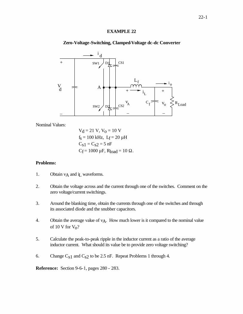
22-1
EXAMPLE 22
Zero-Voltage-Switching, Clamped-Voltage dc-dc Converter
+
_
Vd A
L
i
v
+
_
i d
+
_
v
D1
D2
SW1
SW2A
L
io
CS1
CS2 oCf
f
RLoad
Nominal Values: Vd = 21 V, Vo = 10 V fs = 100 kHz, Lf = 20 µH Cs1 = Cs2 = 5 nF Cf = 1000 µF, Rload = 10 Ω.
Problems: 1. Obtain vA and iL waveforms. 2. Obtain the voltage across and the current through one of the switches. Comment on the
zero voltage/current switchings. 3. Around the blanking time, obtain the currents through one of the switches and through
its associated diode and the snubber capacitors. 4. Obtain the average value of vA. How much lower is it compared to the nominal value
of 10 V for Vo? 5. Calculate the peak-to-peak ripple in the inductor current as a ratio of the average
inductor current. What should its value be to provide zero voltage switching? 6. Change Cs1 and Cs2 to be 2.5 nF. Repeat Problems 1 through 4. Reference: Section 9-6-1, pages 280 - 283.

22-2
PSpice Schematic: ZVSCV Controller:
0
0
0
0
5.5 us 10 us 15.5 us
0.5 us 5 us 10.5 us 15 us
v
vgate2
gate1
[Copyright 2003, Adapted with permission from “Power Electronics Modeling Simplified using PSpice™ (Release 9)”: http://www.mnpere.com]

23-1
EXAMPLE 23
Flyback dc-dc Converter
+
_
N1 N2 C RLoad
+
_
voVd
idiD
+
_
v1
= i o
Nominal Values: Vd = 32 V, Vo ~ 4 V switch duty-ratio D = 0.4, fs = 200 kHz, C = 100 µF, Rload = 1 Ω
Transformer: N1/N2 = 4, Magnetizing inductance Lm = 30 µH, Neglect the leakage inductances. Problems: 1. Obtain waveforms for v1, id, and iD. 2. Plot v1, isw, and iD during a switching transition. 3. Calculate the average values of id and iD in Problem 1 and verify that
IdIo
= VoVd
.
4. Obtain the waveform for the switch voltage vsw. Verify the results with the following
equation:
vsw = Vd1-D .
5. Change the load resistance to 50 Ω and repeat Problems 1 and 2 after a steady state is
reached.

23-2
Reference: Section 10-4-2, pages 308 - 310. PSpice Schematic Flyback NOTE: 1. The transformer of the Flyback converter is represented by a component
XFRM_Linear in the Analog library. Since the leakage inductances are ignored, the coefficient of coupling (k) is assumed to be nearly 1. Therefore,
L1 = 30 µH, and L2 = L1 / (N1/N2)2 = 1.875 µH.
2. An R-C snubber is included across the switch. 3. A 1 MEG resistor is connected to ground at the output to satisfy connectivity
requirements. [Copyright 2003, Adapted with permission from “Power Electronics Modeling Simplified using PSpice™ (Release 9)”: http://www.mnpere.com]

24-1
EXAMPLE 24
Forward dc-dc Converter
+
_
N1 N2 CRLoad
+
_
voVd
idi D1
+
_
v1
N3
D3
D1
f
Lfi L
vL+ _
i3
D2
Nominal Values:
Vd = 50 V, Vo ~ 4.5 V, N1N2
= 4, N1N3
= 1
fs = 200 kHz, Lm = 100 µH, Lf = 7.5 µH Cf = 100 µF, RLoad = 1 Ω, Switch duty-ratio D = 0.4 .
Problems: 1. Obtain the waveforms for iL and the voltage input to the output stage (i.e., the voltage
across diode D2). 2. Obtain v1, isw and i3 waveforms. 3. In problem 2, show that the average value of v1 equals zero. 4. From the results of Problem 2, verify that
tmTs
= N3N1
D
where tm is the time interval during which i3 flows, and Ts is the switching time period.
Reference: Section 10-4-3, pages 311 - 314. PSpice Schematic: Forward

24-2
Notes: 1. The 1-MEG resistor is for satisfying the connectivity requirement. 2. The 3-winding transformer is represented by three inductors L1, L2 and L3 with almost
perfect magnetic coupling. It is represented by a component XFRM_3W. [Copyright 2003, Adapted with permission from “Power Electronics Modeling Simplified using PSpice™ (Release 9)”: http://www.mnpere.com]
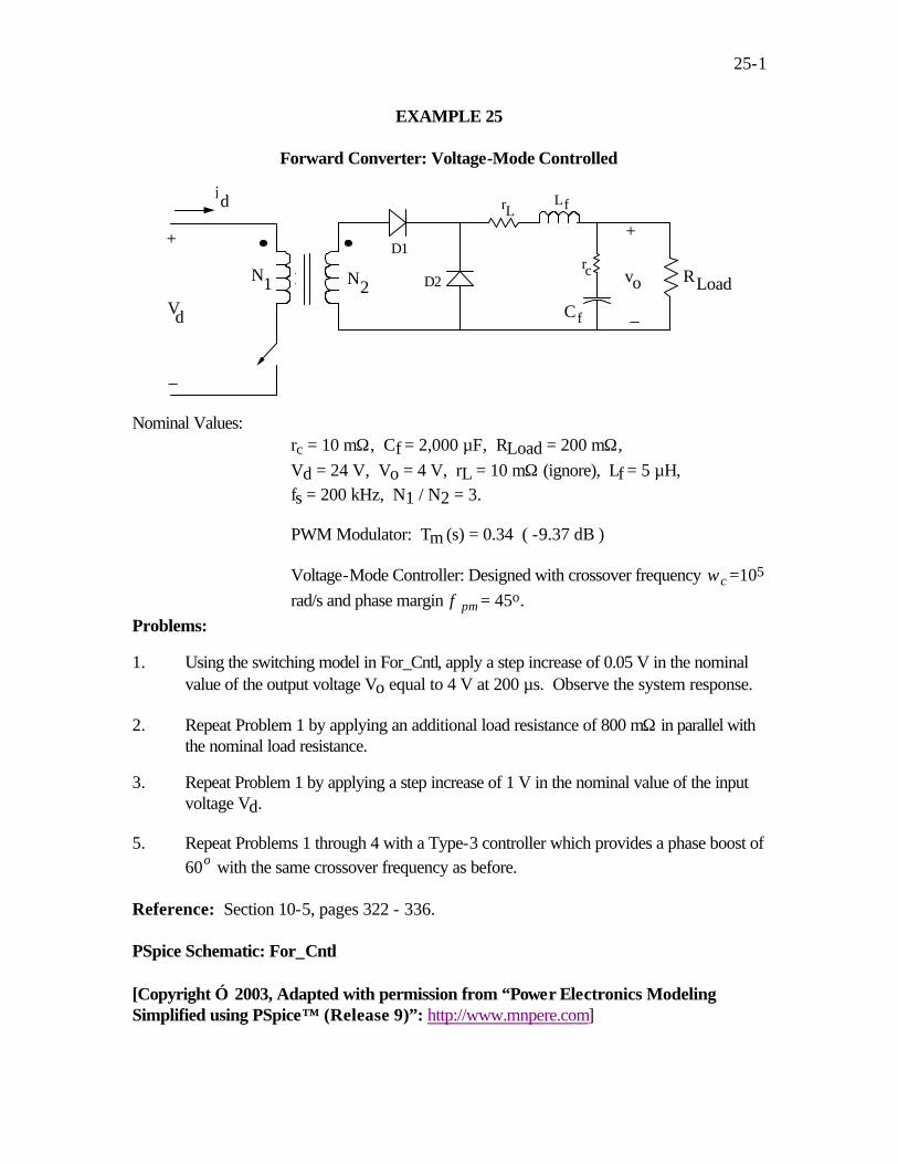
25-1
EXAMPLE 25
Forward Converter: Voltage-Mode Controlled
+
_
N1 N2C
RLoad
+
_
voVd
id
D1
f
Lf
D2
rL
rc
Nominal Values: rc = 10 mΩ, Cf = 2,000 µF, RLoad = 200 mΩ, Vd = 24 V, Vo = 4 V, rL = 10 mΩ (ignore), Lf = 5 µH, fs = 200 kHz, N1 / N2 = 3.
PWM Modulator: Tm (s) = 0.34 ( -9.37 dB )
Voltage-Mode Controller: Designed with crossover frequency ωc =105 rad/s and phase margin φ pm = 45o.
Problems:
1. Using the switching model in For_Cntl, apply a step increase of 0.05 V in the nominal value of the output voltage Vo equal to 4 V at 200 µs. Observe the system response.
2. Repeat Problem 1 by applying an additional load resistance of 800 mΩ in parallel with the nominal load resistance.
3. Repeat Problem 1 by applying a step increase of 1 V in the nominal value of the input voltage Vd.
5. Repeat Problems 1 through 4 with a Type-3 controller which provides a phase boost of 60o with the same crossover frequency as before.
Reference: Section 10-5, pages 322 - 336. PSpice Schematic: For_Cntl [Copyright 2003, Adapted with permission from “Power Electronics Modeling Simplified using PSpice™ (Release 9)”: http://www.mnpere.com]

26-1
EXAMPLE 26
Ripple in the DC Motor Armature Current
+-
+
_
Vd
A
B
N
La Ra
VEMF
i
A1 B1
A2 B2
+
_vo
o
i d
Nominal Values: Vd = 200 V Ra = 0.37 Ω La = 1.5 mH
fs = 10 kHz, Unipolar Voltage Switching KE = KT = 0.75
duty-ratio D1 of TA1 and TB2 = 0.708
(vcontrol = 0.416 V with ^V tri = 1.0 V)
The motor-load is as represented in the schematic DC_Motor. Problems: 1. Obtain the armature current waveform. 2. Calculate peak-to-peak ripple in ia. 3. Repeat Problems 1 and 2 using a Bi-polar-voltage switching scheme. Compare the
results with the unipolar-voltage switching scheme here. 4. Apply a step increase in the control voltage to 0.6V at 0.5 ms and observe the system
response. Reference: Section 13-6-3, pages 388 - 389. PSpice Schematic: DC_Motor [Copyright 2003, Adapted with permission from “Power Electronics Modeling Simplified using PSpice™ (Release 9)”: http://www.mnpere.com]

27-1
EXAMPLE 27
MOSFET Switching Characteristics
In the schematic of MOSFET, the MOSFET is represented by IRF150 MOSFET in EVAL library of PSpice. The diode model within PSpice is used (where all its parameters have default values and rs = 1mΩ). A pulse voltage is applied to the gate of the MOSFET where the rise and fall times are specified as 100 ns. The stray inductance is represented by Lstray.
Problems 1. Look at the MOSFET switching waveforms. 2. Vary Lstray in a range of 20 nH to 200 nH and observe its effect on the switching waveforms. 3. Vary Rgate in a range of 10 Ω to 200 Ω and observe its effect on the switching waveforms. PSpice Schematic: MOSFET [Copyright 2003, Adapted with permission from “Power Electronics Modeling Simplified using PSpice™ (Release 9)”: http://www.mnpere.com]


![KEY-[1991]Novel Soft Switching PWM Converter Using a New Parallel Resonant DC-Link](https://img.pdfslide.net/doc/110x75/55cf96d2550346d0338e00ce/key-1991novel-soft-switching-pwm-converter-using-a-new-parallel-resonant.jpg)