Embed Size (px)
Citation preview

Linköping Studies in Science and TechnologyThesis No 1822
Pulse-Width Modulated RF Transmitters
Muhammad Fahim Ul Haque
Division of Computer EngineeringDepartment of Electrical Engineering
Linköping UniversitySE–581 83 Linköping, Sweden
Linköping 2017

Linköping Studies in Science and TechnologyThesis No 1822
Muhammad Fahim Ul [email protected] of Computer EngineeringDepartment of Electrical EngineeringLinköping UniversitySE–581 83 Linköping, Sweden
Copyright © 2017 Muhammad Fahim Ul Haque, unless otherwise noted.All rights reserved.ISBN 978-91-7685-598-0ISSN 0345-7524IEEE holds the copyright for Papers B, E, and F.
Printed by LiU-Tryck, Linköping, Sweden 2017

To my mother, father, and uncle (mamoo),


Abstract
The market for wireless portable devices has grown significantly over the recentyears. Wireless devices with ever-increased functionality require high rate datatransmission and reduced costs. High data rate is achieved through communi-cation standards such as LTE and WLAN, which generate signals with highpeak-to-average-power ratio (PAPR), hence requiring a power amplifier (PA)that can handle a large dynamic range signal. To keep the costs low, modernCMOS processes allow the integration of the digital, analog and radio functionson to a single chip. However, the design of PAs with large dynamic range andhigh efficiency is challenging due to the low voltage headroom.
To prolong the battery life, the PAs have to be power-efficient as they consumea sizable percentage of the total power. For LTE and WLAN, traditionaltransmitters operate the PA at back-off power, below their peak efficiency,whereas pulse-width modulation (PWM) transmitters use the PA at their peakpower, resulting in a higher efficiency. PWM transmitters can use both linearand SMPAs where the latter are more power efficient and easy to implement innanometer CMOS. The PWM transmitters have a higher efficiency but sufferfrom image and aliasing distortion, resulting in a lower dynamic range, amplitudeand phase resolution.
This thesis studies several new transmitter architectures to improve thedynamic range, amplitude and phase resolution of PWM transmitters withrelaxed filtering requirements. The architectures are suited for fully integratedCMOS solutions, in particular for portable applications.
The first transmitter (MAF-PWMT) eliminates aliasing and image distortionswhile allowing the use of SMPAs by combining RF-PWM and band-limited PWM.The transmitter can be implemented using all-digital techniques and exhibits animproved linearity and spectral performance. The approach is validated using aClass-D PA based transmitter where an improvement of 10.2 dB in the dynamicrange compared to a PWM transmitter for a 1.4 MHz of LTE signal is achieved.
The second transmitter (AC-PWMT) compensates for aliasing distortionby combining PWM and outphasing. It can be used with switch-mode PAs(SMPAs) or linear PAs at peak power. The proposed transmitter shows betterlinearity, improved spectral performance and increased dynamic range as itdoes not suffer from AM-AM distortion of the PAs and aliasing distortion dueto digital PWM. The idea is validated using push-pull PAs and the proposedtransmitter shows an improvement of 9 dB in the dynamic range as compared
v

vi Abstract
to a PWM transmitter using digital pulse-width modulation for a 1.4 MHz LTEsignal.
The third transmitter (MD-PWMT) is an all-digital implementation of thesecond transmitter. The PWM is implemented using a Field ProgrammableGate Array (FPGA) core, and outphasing is implemented as pulse-positionmodulation using FPGA transceivers, which drive two class-D PAs. The digitalimplementation offers the flexibility to adapt the transmitter for multi-standardand multi-band signals. From the measurement results, an improvement of 5 dBin the dynamic range is observed as compared to an all-digital PWM transmitterfor a 1.4 MHz LTE signal.
The fourth transmitter (EP-PWMT) improves the phase linearity of anall-digital PWM transmitter using PWM and asymmetric outphasing. Thetransmitter uses PWM to encode the amplitude, and outphasing for enhancedphase control thus doubling the phase resolution. The measurement setup usesClass-D PAs to amplify a 1.4 MHz LTE up-link signal. An improvement of2.8 dB in the adjacent channel leakage ratio is observed whereas the EVM isreduced by 3.3 % as compared to an all-digital PWM transmitter.
The fifth transmitter (CRF-ML-PWMT) combines multilevel and RF-PWM,whereas the sixth transmitter (CRF-MP-PMWT) combines multiphase PWMand RF-PWM. Both transmitters have smaller chip area as compared to theconventional multiphase and multilevel PWM transmitters, as a combiner isnot required. The proposed transmitters also show better dynamic range andimproved amplitude resolution as compared to conventional RF-PWM transmit-ters.
The solutions presented in this thesis aims to enhance the performance andsimplify the digital implementation of PWM-based RF transmitters.

Populärvetenskaplig sammanfattningMarknaden för trådlösa bärbara enheter har vuxit betydligt under de senasteåren. Ständigt ökad funktionalitet kräver högre dataöverföringshastigheter tillallt lägre pris. Hög hastighet uppnås genom kommunikationsstandarder somLTE och WLAN där signaler med höga topp-till-medeleffektförhållande (PAPR)används, som därför kräver en effektförstärkare (PA) som kan hantera signalermed stort dynamiskt område. För att hålla låg kostnad vill man användamoderna CMOS-processer där digitala, analoga och radiodelar kan integreras påett enda chip. Att konstruera integrerade effektförstärkare i CMOS med stortdynamiskt område och hög energieffektivitet är en utmaning på grund av denlåga spänningen som modern CMOS använder.
För att förlänga batteriets livslängd måste en effektförstärkare ha hög verk-ningsgrad eftersom den förbrukar en betydande andel av en sändares energi. Ikonventionella sändare för LTE och WLAN används effektförstärkare med reduce-rad maximal (avbackad) effekt för att nå linjaritet, vilket sänker verkningsgraden.Genom att använda pulsbreddsmodulering (PWM) kan istället effektförstärka-ren användas vid sin toppeffekt, vilket ger hög verkningsgrad. PWM-baseradesändare kan använda linjära effektförstärkare men också reläkopplade (switchar,switched-mode PA, SMPA) förstärkare som har hög verkningsgrad och är lättaatt konstruera i modern CMOS. PWM-sändarna lider dock av effekter somuppkommer när signaler flyttas i frekvens och digitaliseras, vilket resulterar i ettlägre dynamiskt område och lägre amplitud- och fasupplösning.
I denna avhandling studeras ett flertal nya sändararkitekturer för att för-bättra det dynamiska området, amplitud- och fasupplösning i PWM-sändare.Arkitekturerna är lämpade för fullt integrerade CMOS-realiseringar, i synnerhetför bärbara tillämpningar i t.ex. mobiltelefoner.
Sex olika sändararkitekturer har studerats som på olika sätt förbättrar fre-kvenseffekter, minskar behovet av filtrering, förbättrar verkningsgraden genomatt använda switchade förstärkare eller linjära förstärkare vid toppeffekt, använ-der kretsblock med ren digital teknik, samt har flexibilitet att anpassa sändareför flera olika standarder och olika frekvensband. Genom simuleringar med ettflertal olika verktyg och mätningar på chip och kommersiella förstärkare har deolika koncepten validerats och förbättringar mätts upp.
De sändararkitekturer som presenteras i denna avhandling syftar till attförbättra prestanda och förenkla de digitala realiseringarna i CMOS av PWM-baserade RF-sändare.
vii


Acknowledgments
All praise is due on to Allah, the Compassionate, the most Merciful, the mostGlorious, who gave me physical strength, mental capability, a loving family,skillful teachers, supporting friends and the opportunity to contribute to theever evolving vast body of knowledge. Peace and blessing be upon the HolyProphet Muhammad (Peace be upon Him), the last Prophet of Allah, whoselife is the glorious model for humanity and who exhorted his follower to seekknowledge.
I would like to express my sincere and deepest gratitude towards the followingpeople:
• My supervisor Adj. Prof. Ted Johansson for his guidance, patience andever helping attitude. My research studies started under his supervision,he played the major role in improving my research and academic writingskills. It was an immense pleasure to work and learn from you. I wouldlike to thank him for his untiring efforts and dedication towards my Ph.D.supervision.
• My co-supervisors Prof. Dake Liu and Prof. Qamar Ul Wahab for givingme the opportunity to pursue Ph.D. studies at Linköping University andintroducing me to the area of RF switch-mode power amplifier.
• Assoc. Prof. Oscar Gustafsson for encouraging me to complete my researchgoals. I thank him for his support especially in the final year of my researchstudies.
• Assoc. Prof Tomas Sevensson for his guidance and help throughout myPhD. I am thankful to him, for supporting me during the low times of myresearch studies.
• A very special thanks to Amir Islam, for his regular advice that inculcatedin me spirituality, humbleness, balanced thinking, and straight forwardness.
• Doktorand Muhammad Touqir Pasha for an excellent collaboration inresearch studies. It was a very nice experience to work with him. I thankhim for improving my writing skills.
• Dr. Jahanzeb Ahmad of Intel programmable solutions group for collabora-tion on "Modified All digital PWM transmitters".
ix

x Acknowledgments
• Doktorand Saima Athar, for her support during my PhD studies. Shehelped and guided me like a younger brother. I would also like thank herfor teaching me the basics of cooking.
• Dr. Nadeem Afzal, Dr. Fahad Qureshi and Ali Saeed for all their supportand help during my early days in Linköping which helped me to settle inthis city.
• ISY administrators Gunnel Hässsler, Susanna von Sehlen and Ylva Jernlingfor helping out with the administrative tasks.
• Arta Alvandpour for his help in setting up the chip design tools and forarranging the test equipment.
• Anders Nilsson for his help with the office computer and equipment. Healso helped me in preparing the PCBs for measurements.
• All the teachers who played an important part in my learning. Few ofthem who had a profound impact on me Prof. Abdul Rauf Khan, Prof.Saad Qazi, Prof. Abdul Qadir, Prof Zainab Zaidi, Prof. Atila Alvandpour,Prof. Håkan Johansson, Assoc. Prof. Kent Palmkvist, Assoc. Prof. JerzyDabrowski, Assoc. Prof. Mikael Olofsson, Assoc. Prof. Muhammad ImranAslam, Assoc. Prof. Shehzad Hasan, Asst. Prof. Muhammad Asad Arfeen,Asst. Prof. Saneeha Ahmed, Asst. Prof. Amir Zeb, Asst. Prof. ShahzadSiddiqi and Dr Mehnaz.
• The former and current colleagues at Computer Engineering division,Linköping university for their help, support and creating a friendly en-vironment. I would specially give my gratitude to Assoc. Prof. MarioGarrido, Dr. Andeas Karlssson, Dr. Muhammad Irfan Kazim, Dr. AmeyaBhide, Dr. Hashim Raza Khan, Dr. Fahad Qazi, Dr. Zaka Ullah, Dr.Muhammad Abbas, Dr. Shakila Bint Riaz, Doctorand Petter Källström,Doctorand Carl Ingemarsson and Doctrand Erik Bertilsson.
• My friends outside Linköping for morally supporting me and rememberingme in prayers. I especially thank Moosa Kaleem, Dr. Tahir Malik, MasroorAli, Muhammad Fahim, Abbas Zaidi, Waqas Saeed, Dr Ahmad AhsanNawaz, Noman Ahmed, Zeeshan Malik and Rahul Anil Nadgouda.
• My current and former corridor mates for create a very friendly environ-ment for living. I would specially give my gratitude to Matti Lundgren,

Acknowledgments xi
Hampus Billing, Li-Yu Chen, Erica Stigell, Fedrik Källgren, Nasir Zaman,Ishtiaq Hussain, Abdus Sami, Karthikeyen Srinivasan and Nandu.
• Finally a special thanks to my family
− My Mother, Quaisar Perveen for her sacrifices, immense love, andsupport. She played a pivotal part in my upbringing. Throughouther life she supported me and prayed for me.
− My uncle Dr. Muhammad Sami Hyder for all his love, support andguidance. He motivated me to pursue higher studies. He alwaysbacked my decisions regarding my career. He acted both as a fatherlyfigure and a friend throughout my life.
− My father Muhammad Nasim Ul Haque for all his love, support andguidance. He gave me room to make my independent decisions andsupported me on them. He always guided throughout my life.
− My sister Humera Nasim for her love, moral support and prayers.
− My brothers and cousins Muhammad Rizwan Ul Haque, MuhammadNauman Hyder and Muhammad Zeeshan Hyder for their love.
I always thank Allah to bless me such a loving and supporting family.
• To all those not listed here, I thank you for enriching my life.
Muhammad Fahim Ul HaqueJanuary 17, 2017,Linköping Sweden


Preface
This Ph.D thesis is based on the work presented in the following publications.
• Paper A M. F. Ul Haque, M. T. Pasha, T. Johansson, "A Power effi-cient aliasing-free PWM transmitter", submitted to IEEE Transactions onMicrowave Theory and Technique.
• Paper BM. F. Ul Haque, M. T. Pasha, T. Johansson, "Aliasing-CompensatedPolar PWM Transmitter," accepted for publication in IEEE Transactionson Circuits and Systems II: Express Briefs, Sep 2016.
• Paper C M. T. Pasha, M.F. Ul Haque, T. Johansson, "A modified all-digital polar PWM transmitter", submitted to IEEE Transactions onCircuits and Systems I.
• Paper D M. F. Ul Haque, M. T. Pasha, T. Johansson, "An all-digitalPWM transmitter with enhanced phase resolution", submitted to IEEEMicrowave and Wireless Components Letters.
• Paper E M. F. Ul Haque, T. Johansson and D. Liu, "Combined RF andmultilevel PWM switch mode power amplifier," presented at NORCHIP,Vilnius, 2013.
• Paper F M. F. Ul. Haque, T. Johansson and D. Liu, "Combined RFand multiphase PWM transmitter," presented at European Conference onCircuit Theory and Design (ECCTD), Trondheim, 2015.
The following publications are not included in this thesis. The work of thesepublications partially overlaps with the appended papers or is out of the scopeof this thesis.
xiii

xiv Preface
• M. F. Ul Haque, T. Johansson, "Power efficient and large dynamic rangeRF-PWM transmitter," Swedish Microwave Days - Giga Hertz and AntennaEMB Symposium, March 2016, Linköping, p. 34, 2016.
• M. F. Ul Haque, T. Johansson, "Modified band-limited pulse-width modu-lated polar transmitter," presented at ISMOT, Dresden, July 2015.
• M. F. Ul Haque, T. Johansson and D. Liu, "Power efficient band-limitedpulse-width modulated transmitter," presented at Swedish System on ChipConference, May 4-5 2015, Göteborg.
• M. F. Ul Haque, T. Johansson and D. Liu, "Modified multilevel PWMswitch mode power amplifier," presented at Swedish System on ChipConference, Vadstena, May 12-13, 2014.

Contents
Background 1
1 Introduction 31.1 Motivation . . . . . . . . . . . . . . . . . . . . . . . . . . . . . . 31.2 Organization of Thesis . . . . . . . . . . . . . . . . . . . . . . . . 51.3 Wireless Transmitter . . . . . . . . . . . . . . . . . . . . . . . . . 6
1.3.1 Direct Conversion Transmitter . . . . . . . . . . . . . . . 61.3.2 Heterodyne Transmitter . . . . . . . . . . . . . . . . . . . 6
1.4 Performance Parameters for Wireless Transmitters . . . . . . . . 71.4.1 Output Power . . . . . . . . . . . . . . . . . . . . . . . . . 81.4.2 Type of Modulated Signal . . . . . . . . . . . . . . . . . . 81.4.3 Efficiency . . . . . . . . . . . . . . . . . . . . . . . . . . . 91.4.4 Linearity . . . . . . . . . . . . . . . . . . . . . . . . . . . 9
1.5 RF Power Amplifier . . . . . . . . . . . . . . . . . . . . . . . . . 101.5.1 Linear PAs . . . . . . . . . . . . . . . . . . . . . . . . . . 111.5.2 Switch-Mode PA . . . . . . . . . . . . . . . . . . . . . . . 13
1.6 Fabrication Technology for RF PAs . . . . . . . . . . . . . . . . . 16
2 Transmitter Architectures for Linearization of Power-EfficientAmplifiers 192.1 Polar Modulation . . . . . . . . . . . . . . . . . . . . . . . . . . . 192.2 Outphasing . . . . . . . . . . . . . . . . . . . . . . . . . . . . . . 21
2.2.1 Outphasing Issues . . . . . . . . . . . . . . . . . . . . . . 222.3 Pulse-Width Modulation . . . . . . . . . . . . . . . . . . . . . . . 26
3 Pulse-Width Modulation Based Transmitter 273.1 Radio-Frequency PWM Transmitter . . . . . . . . . . . . . . . . 273.2 Polar PWM Transmitter . . . . . . . . . . . . . . . . . . . . . . . 29
xv

xvi Contents
3.2.1 Concept . . . . . . . . . . . . . . . . . . . . . . . . . . . . 293.2.2 Efficiency . . . . . . . . . . . . . . . . . . . . . . . . . . . 303.2.3 Polar PWT Transmitter Issue . . . . . . . . . . . . . . . . 33
4 Polar PWM Transmitters with Reduce Image and Aliasing Dis-tortion 414.1 Image-Distortion Free Polar PWM Transmitter . . . . . . . . . . 42
4.1.1 Exploiting Image Gap . . . . . . . . . . . . . . . . . . . . 424.1.2 Elimination of Image Distortion . . . . . . . . . . . . . . 42
4.2 Aliasing-Free PWM Transmitter . . . . . . . . . . . . . . . . . . 444.2.1 Concept . . . . . . . . . . . . . . . . . . . . . . . . . . . . 444.2.2 Efficiency . . . . . . . . . . . . . . . . . . . . . . . . . . . 46
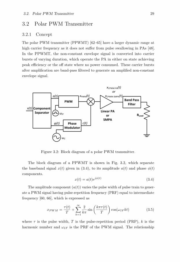
4.3 Combined RF and AF-PWM Transmitter . . . . . . . . . . . . . 494.4 Aliasing-Compensated PWM Transmitter . . . . . . . . . . . . . 514.5 Simulation Results . . . . . . . . . . . . . . . . . . . . . . . . . . 524.6 Enhanced Phase Resolution All-Digital PWM Transmitter . . . . 54
5 Polar PWM Transmitters withRelaxed Band-Pass Filtering 575.1 Multi-Level PWM Transmitter . . . . . . . . . . . . . . . . . . . 57
5.1.1 Concept . . . . . . . . . . . . . . . . . . . . . . . . . . . . 575.1.2 Efficiency . . . . . . . . . . . . . . . . . . . . . . . . . . . 59
5.2 Multi-Phase PWM Transmitter . . . . . . . . . . . . . . . . . . . 615.2.1 Concept . . . . . . . . . . . . . . . . . . . . . . . . . . . . 615.2.2 Efficiency . . . . . . . . . . . . . . . . . . . . . . . . . . . 63
5.3 Combined RF and ML-PWM Transmitter . . . . . . . . . . . . . 635.4 Combined RF and MP-PWM Transmitter . . . . . . . . . . . . . 65
6 Conclusions and Future Trends 67
References 71
Publications 79
A A Power-Efficient Aliasing-Free PWM Transmitter 81
B Aliasing-Compensated Polar PWM Transmitter 91
C A Modified All-Digital Polar PWM Transmitter 99

Contents xvii
D An All-digital PWM Transmitter with Enhanced Phase Reso-lution 111
E Combined RF and Multilevel PWMSwitch Mode Power Amplifier 117
F Combined RF and multiphase PWM Transmitter 123


Background


Chapter 1
Introduction
1.1 MotivationWireless communication technology is continuously evolving and has becomean integral part of daily life. High data rate applications like high definitionvideo streaming and online gaming place high demands on modern wirelesscommunication systems. The demand for wireless communications has increasedexponentially in the previous years and is set to further increase with the adventof remote healthcare, internet of things, autonomous cars and virtual realityapplications.
The wireless operators aim to reduce the operating costs for their networksby using energy-efficient radio base stations (RBS). The power amplifiers (PAs)consume the major power of an RBS, so using power-efficient PAs would resultin a lower power consumption hence reducing the operation cost. Low-efficiencyPAs not only increase the power consumption but the heat generated fromthem contributes to long-term reliability issues. From a user’s viewpoint, low-efficiency PAs lead to a shorter battery life and the excessive heat dissipationposes a challenge to the efforts of making wireless devices more portable.
Typically, CMOS has been the technology of choice for implementing digitalcircuits due to low cost and high levels of integration. The analog and RFcircuits have typically been designed using silicon bipolar devices and GaAs dueto their performance characteristics. However, due to the rapid scaling of CMOSprocess, the transition frequency of CMOS devices has been pushed beyond 100GHz and gradually the CMOS implementations of RF circuits have become
3

4 Chapter 1.
popular. To reduce the cost and achieve a full radio system-on-chip (SoC),it is desirable to integrate both the digital baseband and the PAs on a singlechip. As the PA is the highest power-consuming component in a transceiver,its power efficiency is an important requirement. A power-efficient PA not onlyprolongs the battery life but also dissipates less heat thus lowering packagingcosts, increasing reliability and allowing for further integration.
To increase the bandwidth utilization, modern wireless standards use complexmodulation with multiplexing schemes like quadrature amplitude modulation(QAM) and orthogonal frequency division multiplexing (OFDM). These schemesgenerate high peak to average power ratio (PAPR) signals which place strictlinearity requirements, forcing the use of linear PAs at back-off at which theirefficiency drops drastically, thus decreasing the average efficiency of transmitter.Switch-mode PAs (SMPAs) are an attractive alternative as they can operateat zero losses, ideally resulting in highly efficient transmitters. However, theycan only be used with constant-envelope signals and require schemes for thetranslation of non-constant envelope to constant-envelope signals.
Pulse-Width Modulation (PWM) was originally introduced in audio amplifiersto increase the efficiency by replacing the conventional linear amplifiers withSMPAs. The results encouraged the use of PWM for RF applications where itis used to encode the amplitude information. The PWM can be used at RF andbaseband frequencies, each with its own advantages and trade-offs.
For the transmitters using PMW at RF frequencies (RF-PWM) [1], theharmonics appear at integer multiples of the carrier frequency thus relaxing theband-pass filtering requirements. However, at higher carrier frequencies the RF-PWM based transmitters have a lower dynamic range due to pulse-swallowing,which is related to limited switching frequency of the circuit.
Transmitters using PWM at baseband (polar PWM or carrier-based PWM) [2]do not suffer from pulse swallowing as the modulation is done at IF, whichis up-converted to an RF signal with a fixed duty cycle. However, since theharmonics appear at multiples of IF frequencies a higher order band-pass filteringis required. In addition, the infinite bandwidth of the PWM also introducesimage and aliasing distortion, thus deteriorating the transmitter linearity.
This thesis aims to relax the filtering requirements and enhance the linearityof polar PWM transmitters. The focus has been to use all-digital techniquesto develop multi-standard flexible transmitters. In total, six transmitters havebeen developed that compensate for aliasing and image distortions and simplifythe design requirements.

1.2. Organization of Thesis 5
1.2 Organization of ThesisThis thesis is divided into two sections. The background section provides a briefoverview to the target research area and is composed of the following chapters:
• Chapter 1 discusses the wireless transmitter, the performance param-eters for transmitters, major classes of power amplifiers and fabricationtechnology for RF PAs.
• Chapter 2 discusses transmitter architectures that allow power-efficientamplification of non-zero PAPR signals.
• Chapter 3 discusses the PWM transmitter and its issues.
• Chapter 4 discusses variants of PWM transmitters that reduce imageand aliasing distortion. This chapter also includes a brief overview of theproposed transmitters presented in Paper A-D.
• Chapter 5 discusses PWM transmitters that have relaxed filtering re-quirements and high amplitude resolution. This chapter also includes abrief overview of the proposed transmitters presented in Paper E and F.
The publications section collects the papers that are a result of the thesis. Abrief overview of each of the papers is given as:
• Paper A presents a transmitter that combines band-limited PWM andRF PWMT to reduce aliasing distortion while achieving an efficiencycomparable to a PWM based transmitter. The paper also discusses anall-digital implementation of the transmitter.
• Paper B combines PWM and outphasing to reduce the image and ampli-tude aliasing distortions while achieving efficiency comparable to a PWMbased transmitter.
• Paper C is about an all-digital implementation of the aliasing-compensatedPWM transmitter.
• Paper D combines PWM and asymmetric outphasing to improve phaseresolution of all-digital PWM transmitters.
• Paper E combines multilevel PWM and RF PWM to achieve higheramplitude resolution, better efficiency and smaller chip area.
• Paper F combines multiphase PWM and RF PWM to relax final filteringrequirements and to reduce the chip area.

6 Chapter 1.
1.3 Wireless TransmitterThe wireless transmitter processes, up-converts and amplifies the informationsignal to the desired carrier frequency and power. The two major architec-tures of conventional transmitters are the direct conversion transmitter and theheterodyne transmitter.
1.3.1 Direct Conversion Transmitter
The block diagram of the direct conversion transmitter for digital communicationis shown in Fig. 1.1. The transmitter separates the digital baseband signal intoquadrature components I(n) and Q(n), which are then converted into analogsignals I(t) and Q(t) using a digital to analog convertor (DAC). These signalsare then mixed with quadrature phase-shifted carriers to generate quadratureup-converted signals at a transmit frequency (ωT ), as given in (1.1). Thesesignals are combined to generate an amplitude and phase modulated carrier,expressed in (1.2). This modulated signal is then amplified to a desired powerand finally filtered to generate the transmitted signal. The filtering is doneto suppress the out-of-band leakage, which occurs due to non-idealities of thetransmitter. The major issues of the transmitter are I/Q mismatch, carrierleakage, oscillator pulling, mixer non-linearity and PA non-linearity. [3, 4]
v1(t) = I(t) cos(ωT t) (1.1a)
v2(t) = Q(t) sin(ωT t) (1.1b)
v(t) = I(t) cos(ωT t)−Q(t) sin(ωT t) = a(t) cos (ωT t+ φ (t)) (1.2)
where
a(t) is the Amplitudeφ(t) is the Phase
1.3.2 Heterodyne Transmitter
As contrast to the direct-conversion transmitter, the heterodyne transmitterperforms two up-conversions in order to transmit the information at the desiredfrequency. The block diagram of the heterodyne transmitter for digital commu-nication is shown in Fig. 1.2. The transmitter separates the baseband signal intoquadrature components, which are up-converted to intermediate frequency (ω1)and then combined to generate an amplitude and phase modulated signal at

1.4. Performance Parameters for Wireless Transmitters 7
Band Pass
Filter
RLoad
Splitter
IDAC
X
DACQ
90o
PA-
Figure 1.1: Block diagram of a direct conversion transmitter.
(ω1), which is given as (1.3). This signal is again up-converted to translate theinformation to the transmit frequency (ωT ), which is given as (1.4). The twoup-conversions are performed to reduce the effect of oscillator pulling. The signalis then amplified and filtered to generate the transmitted signal. The majorissues of this type of transmitters are carrier leakage and mixing spurs. [3, 4]
v1Mix(t) = a(t) cos (ω1t+ φ (t)) (1.3)
v2Mix(t) = 12a(t) cos ((ω1 + ω2) t+ φ (t)) + cos ((ω2 − ω1) t+ φ (t)) (1.4)
where
ωT = ω1 + ω2
Band Pass
Filter
RLoad
Splitter
IDAC
X
DACQ
90o
PA-
Figure 1.2: Block diagram of a heterodyne transmitter.
1.4 Performance Parameters for Wireless TransmittersThe performance of a transmitter is usually characterized by its output power,type of modulated signal, efficiency and linearity. Next each of these parametersare described briefly.

8 Chapter 1.
1.4.1 Output Power
Output power is the power delivered to the antenna at desired frequency bandand is usually guided by the type of the end-user application. The PA is themajor block that determines the output power of the transmitter. It must benoted that due to subsystem imperfections, mismatch and PA characteristics,the transmitter might leak power outside the desired transmission band. Aband-pass filter is used to attenuate these leakage power.
1.4.2 Type of Modulated Signal
There are two type of modulated signals in general: a constant-envelope modu-lated signal and a non-constant envelope modulated signal, as shown in Fig. 1.3.The constant-envelope signals are generated by modulation schemes like M-PSK,FSK and GMSK used in GSM cellular networks. The advantage of constant-envelope signals is that they are not corrupted by the PA non-linearity. Thenon-constant envelope signals are generated by modulation schemes like ASK,M-QAM or a combination of M-QAM and OFDM, which is used in standardslike 802.11, LTE, etc. The advantage of non-constant envelope modulation isbandwidth efficiency. However, these signals are prone to PA non-linearity. [5]
Time
Am
plit
ude
(a)Time
Am
plit
ude
(b)
Figure 1.3: (a) Constant-envelope signal, (b) Non-constant envelope signal.
The PAPR determines the amount of envelope variation in the non-constantenvelope signal and is defined as the ratio of peak output power (Ppeak) toaverage output power (Pavg), which is given as
PAPRdB = 10 log10
(PpeakPavg
). (1.5)

1.4. Performance Parameters for Wireless Transmitters 9
1.4.3 Efficiency
As the transmitter consumes most of the power of a transceiver, the efficiency ofthe transmitter determines the battery life in case of portable devices and theenergy cost in case of RBS.
Two measure of efficiency i.e, drain efficiency (DE) and power added efficiency(PAE) are interchangeably used when characterizing transmitter. The drainefficiency [5–7] is ratio the transmitter’s output power Pout to the consumedDC power Pdc and is given as
DE = PoutPdc
. (1.6)
The power added efficiency [5–7] is ratio of the difference between outputpower and input power Pin to the dc power consumption and is given as
PAE = Pout − PinPdc
. (1.7)
1.4.4 Linearity
The linearity of a transmitter is important for the accuracy of the transmittedsignal. In case of constant-envelope signals, phase linearity is an importantparameter, whereas for non-constant envelope signals both phase and amplitudelinearity are important. The two common parameters to measure the linearityof the transmitter are adjacent channel leakage ratio (ACLR) and error vectormagnitude (EVM).
The ACLR [5, 7] is the ratio of the average powers in the transmission bandto the adjacent bands. Fig. 1.4 shows the the measured spectrum and measuredACLR for a 1.4 MHz LTE up-link signal.
The EVM [5, 7] determines the error between the measured transmit signal(in case of transmitter) and the reference signal. It is defined as the ratio of theerror vector (Verror) to the reference signal vector (Vref ). The EVM is eitherexpressed in percentage as given in (1.8) or in dB as in (1.9).
EVM(%) =(VerrorVref
)× 100 (1.8)
EVM(dB) = 20 log(VerrorVref
)(1.9)
where error vector and reference vector are determined from the I/Q constellationplot as shown in Fig. 1.5

10 Chapter 1.
Figure 1.4: Measured spectrum and ACLR for 1.4 MHz LTE up-link signal.
Verror
Vref
Reference
Signal
Measured
Signal
I
Q
Figure 1.5: EVM measurement from I/Q constellation plot.
1.5 RF Power Amplifier
The type of PA used in the transmitter has a profound effect on the performanceof the transmitter. Each type of PA has different performance characteristicsand it is usually up to the designer to select the most suitable type of PA forthe target application. The PAs are broadly classified into two categories: linearPAs and switch mode PAs.
1.5. RF Power Amplifier 11
1.5.1 Linear PAs
These PAs are also called classical PAs, and use devices as a controlled currentsource. The general schematic of a linear PA is shown in Fig. 1.6 and basedon the transistor biasing they are categorized in to three major classes, namelyClass A, B, C and the subclass AB. [6, 8, 9]
LRF choke
CDC block
RLC
L
Tune
Network
VDD
VIN
VDS
ID
Figure 1.6: Linear PAs schematic.
1.5.1.1 Class A
Class A PAs [10, 11] are normally used for applications that require very highlinearity. Class A PAs adjust the quiescent point (Q-point) of the transistorsuch that it does not turn off throughout the input signal cycle. The typicalwaveforms for the drain voltage and current are shown in Fig. 1.7. These PAshave the best linearity and the lowest efficiency among all PA classes. The peakefficiency of an ideal Class A PA is 50% at peak power which decreases as theoutput power reduces below the peak values. The normalized power outputcapability is the measure of device stress and defined as the ratio of the outputpower to the product of maximum drain voltage and current for the device(higher is better) [12]. In case of class A PA it is 0.125.
1.5.1.2 Class B
For Class B PAs the Q-point is adjusted such that the device is turned off duringhalf of the input cycle period. The typical waveforms for the drain voltageand current are shown in Fig.1.8. Due to the simultaneous occurrence of drainvoltage and current for only half the period, Class B PAs have a higher efficiencyand lower linearity as compared to Class A PAs. These PAs require high quality

12 Chapter 1.
0
2
Time
VD
S
(a)
0
2
Time
I D
(b)
Figure 1.7: Class A waveform for (a) drain voltage, (b) drain current.
0
2
Time
VD
S
(a)
0
2
Time
I D
(b)
Figure 1.8: Class B waveform for (a) drain voltage, (b) drain current.
factor tuned network such that the harmonics due to clipped sine wave arefiltered to generate a sine wave. The peak efficiency of an ideal Class B PA is78.5% and normalized power output capability is 0.125. [11–13]
1.5.1.3 Class C
In Class C PAs the Q-point is biased such that the transistor is active for lessthan half of the input signal period. As a result the efficiency is improvedbut with reduced power and degraded linearity. The typical waveforms for thedrain voltage and current are shown in Fig.1.9. Ideal Class C PAs efficiencydepend on conduction angle, in case of 150o conduction angle, it achieves 85%efficiency. [11–13]
1.5.1.4 Class AB
The Q-point for Class AB PAs is biased such that the transistor is turned onfor more than half of the input clock period unlike Class-B PAs but not for the

1.5. RF Power Amplifier 13
0
2
Time
VD
S
(a)
00
4
Time
I D
(b)
Figure 1.9: Class C waveform for (a) drain voltage, (b) drain current.
entire input cycle like Class-A PAs. This amplifier is compromise between classA and class B PAs and achieves higher linearity and efficiency as compared toClass B and Class A PAs respectively. [8, 14–16]
1.5.2 Switch-Mode PA
SMPAs use devices as switches that are either in the on or off state. They havehigher efficiency as compared to linear PAs. However, they can only amplifyconstant-envelope signals. They are categorized in three major classes, namelyClass D, E and F. [8, 9]
1.5.2.1 Class D
Class D PAs [17–19] use transistors in a switching configuration to generatea square drain-voltage waveform, which is filtered to generate a sinusoid offundamental frequency at the output. A typical inverter-based Class D im-plementation is shown in Fig. 1.10 and the corresponding waveforms for thedrain voltage and current are shown in Fig. 1.11. Since the voltage and currenthave a complimentary relation the ideal Class D PA can achieve 100% efficiency.However, due to finite switching speeds of the output stage the drain voltage andcurrent regions overlap, causing losses. The normalized power output capabilityof Class D PAs is 0.32. [12, 20, 21]
1.5.2.2 Class E
Class E PAs [22–24] use a tuning network to reduce the losses due to finiteswitching speed of the transistor. The tuning network for the Class E PA is

14 Chapter 1.
C1
RL
Tune
Network
VDD
VIN
VDS
IP
L1
IN
Figure 1.10: Schematic of a Class D PAs.
0
1
Time
VD
S
(a)
0
1
Time
I D
(b)
Figure 1.11: Class D waveform for (a) drain voltage, (b) drain current.
designed such that it meets the conditions given below
vC(t)|t= 2πωo
= 0 (1.10a)
dvc(t)dt
∣∣∣t= 2π
ωo
= 0 (1.10b)
The (1.10a) ensures no losses occur due to the discharging of the draincapacitance at off to on switching instance, whereas (1.10b) ensures that nocurrent flows through the transistor at off to on switching instance. As a result,the practical Class E PAs may have a higher efficiency compared to Class DPAs. However the disadvantage of Class E PA is a lower power utilization factor,which is 0.098. A typical implementation of the Class E PA is shown in Fig. 1.12and its corresponding waveforms are shown in Fig 1.13.

1.5. RF Power Amplifier 15
C2
RL
L2+LX
VIN
VDS
ID
L1
VDD
C1
Figure 1.12: Schematic of a Class E PAs.
3.5
Time
VD
C
(a)
1.6
Time
I D
(b)
Figure 1.13: Class E waveform for (a) drain voltage, (b) drain current.
1.5.2.3 Class F
Class F PAs also use a tuning network to reduce the transistor switching lossesby shaping the drain voltage and current waveforms. A typical implementationof the Class F PA is shown in Fig. 1.14, where a tuned network consisting of aλ/4 transmission line and a parallel tank circuit is used The tuning network onlyallows the fundamental frequency to pass to the load, while the odd harmonicsare terminated by the infinite resistance and even harmonics are terminated byzero resistance. As a result, the transistor drain voltage is a square waveformand drain current is a half-wave sinusoid, as shown in Fig.1.15. It can be seenthat the drain current and voltage do not occur simultaneously at the switchinginstance hence this class of PAs have a higher efficiency. The normalized poweroutput capability of a Class F PA is 0.16 which is higher than Class E PA.However, on-chip implementation of a Class F PA is difficult due to the tunednetwork. [24, 25]

16 Chapter 1.
LRF choke
RLCLTune
Network
VDD
VIN
VDS
ID/4 at ωC
Figure 1.14: Schematic of Class F PAs.
0
2
Time
VD
S
(a)
0
2.5
Time
I D
(b)
Figure 1.15: Class F waveform for (a) drain voltage, (b) drain current.
1.6 Fabrication Technology for RF PAs
Many of the RF PAs are used in combination with digital circuits used forpre-distortion to maintain their linearity and efficiency. Typically, RF circuitswere fabricated using bipolar devices due to higher performance characteristicswhereas CMOS has been favored for the implementation of the supportingdigital circuits due to its higher density. This led to the introduction of BiCMOSprocesses that combined the characteristics of bipolar and CMOS technology.However, the BiCMOS processes are not preferred today due to the addedcomplexity in the fabrication process.
Typically, CMOS processes were not preferred for the fabrication of RFcircuits due to low transition frequency and inadequate performance. However,as the transition frequency of CMOS has increased due to process scaling henceits RF performance has also improved. For wireless consumer markets cost,

1.6. Fabrication Technology for RF PAs 17
product size and power consumption are the main driving parameters, thusmaking CMOS a technology of choice for these applications. Although the RFperformance of semiconductors like GaN and GaAs is very high as compared toCMOS, but they are preferred in high-requirement applications, such as RBSand satellite applications. Fully integrated CMOS wireless transceiver havebecome quite common for portable devices [26, 27].


Chapter 2
Transmitter Architectures for Linearization ofPower-Efficient Amplifiers
The performance of wireless devices is characterized by data rates and powerconsumption. High data rates are achieved though spectral-efficient communi-cation standards like 802.11 and LTE, which generate non-constant envelopesignals that are amplified using highly efficient PAs, which play an importantrole in maximizing the battery life by reducing the power losses.
As discussed in chapter 1, PAs are categorized into two broad categories:linear PAs and switch-mode PAs (SMPA). The linear PAs amplify non-constantenvelope signals but have low peak efficiency. Moreover, their efficiency furtherdecreases at back-off power. SMPAs on the other hand are highly power-efficientdue to on-off operation of the transistors. However, they can only be used toamplify constant-envelope signals.
Several transmission schemes have been developed that are highly powerefficient as they allow the amplification of non-constant envelope signals eitherusing SMPAs or linear PAs operating at saturated power. Popular transmissionschemes that are efficient for non-constant envelope signals are polar modulation,outphasing and pulse-width modulation.
2.1 Polar ModulationThe polar modulation or envelope elimination and restoration (EER) was firstintroduced by Kahn in 1952 [28], and therefore also referred as Kahn transmitter.
19

20 Chapter 2.
ENVELOPE
DETECTOR
LIMITER SMPA
RL
Venv
Vcarr
Vin
Vout
Figure 2.1: Block diagram of a polar modulation transmitter.
The conceptual block diagram is shown in Fig. 2.1. The pass-band signal given in(2.1) is split into a low-frequency envelope signal venv(t) and a constant-envelopephase-modulated signal vcarr(t), given in (2.2) using the envelope detector andthe limiter respectively. The phase modulated signal is power amplified by anSMPA, where venv(t) varies the supply voltage of the SMPA. Hence the finaltransmitted signal is the amplified version of (2.1) and can be expressed as (2.3).This technique allows the amplification of non-constant envelope signals throughSMPAs, resulting in a better power efficiency as compared to conventionaltransmitters.
v(t) = venv(t) cos (ωct+ φ (t)) (2.1)
where
ωc is the carrier frequency in radian/sec
vcarr(t) = cos (ωct+ φ (t)) (2.2)
vout(t) = Avenv(t) cos (ωct+ φ (t)) (2.3)
A common implementation of the polar modulation transmitter [29–32],shown in Fig. 2.2, decomposes the baseband signal into amplitude (venv(t)) andphase (φ(t)) components. The φ(t) phase modulates the carrier, which is thenamplified by an SMPA and its supply voltage is varied by venv(t). The majoradvantage of this implementation is that the envelop detector and the limiterare not required, hence the non-linearity due to the envelope detector and theAM/PM conversion due to the limiter are avoided.

2.2. Outphasing 21
Phase
ModulatorSMPA
RL
Venv(t)
Vcarr
Vout
CORDIC
φ(t)
Venv(t)< φ(t)
Figure 2.2: Common implementation of a polar modulation transmitter.
However, the performance of polar modulators is affected by the delaymismatch between envelope and phase-modulated carrier paths and varyingoutput capacitance due to the PA supply voltage variations. Apart from thesefactors, maintaining high efficiency for wide bandwidth signal and achievinglarge dynamic range in low voltage head room CMOS technology is a challenge.
2.2 Outphasing
Outphasing or linear amplification with non-linear components (LINC) [28, 32–34] decomposes a non-constant envelope signal into two constant-envelope signals,and allows the use of SMPAs or highly saturated linear PAs operating at theirpeak efficiency for amplification.
The Fig. 2.3 shows the basic idea of outphasing, in which the non-constant en-velope signal, vin(t) in (2.4), is first decomposed into two phase-shifted constant-envelope signals, v1(t) and v2(t) given in (2.5), where the phase shift θ(t) (calledthe outphasing angle hereafter) is determined by the instantaneous envelopesignal a(t). The relationship between θ(t) and a(t) is expressed in (2.6). Theconstant-envelope signals v1(t) and v2(t) are then amplified by the power-efficientPAs and combined by a passive combiner to generate the amplified version ofthe input signal.
vin(t) = a(t) cos (ωct+ φ (t)) (2.4)

22 Chapter 2.
PA1
RL
PA1
Signal
DecomposerSignal
Decomposer
Vin Vout
V1
V2
Figure 2.3: Block diagram of an outphasing transmitter.
v1(t) = 12 cos (ωct+ φ(t) + θ(t)) (2.5a)
v2(t) = 12 cos (ωct+ φ(t)− θ(t)) (2.5b)
θ = cos−1 (a (t)) (2.6)
2.2.1 Outphasing Issues
For outphasing transmitters, mismatch issues in the amplification path and thecombiner design play a critical role in determining the transmitter efficiency andlinearity.
2.2.1.1 Amplification paths mismatch
The path mismatch is the gain and phase mismatches between the two amplifi-cation paths in Fig. 2.3, which results in signal distortion and spectral regrowthat the output of transmitter [32]. The two mismatches result in an amplitudedifference ∆A and an additional phase difference the ∆θ between the two am-plified phase-shifted signals, which mathematically can be expressed as (2.7).The combination of the two signals is expressed in (2.8), which shows the signaldistortion and spectral regrowth due to the paths mismatches.
v1(t) =(A
2 + ∆A)
cos (ωCt+ φ (t) + θ (t) + ∆θ) (2.7a)
v2(t) = A
2 cos (ωct+ φ(t)− θ(t)) (2.7b)

2.2. Outphasing 23
vout(t) = v1(t) + v2(t)
= ∆A cos (ωct+ φ (t) + θ (t) + ∆θ) +Aa (t) cos (ωct+ φ (t))
−Aa (t) sin2(
∆θ2
)cos (ωct+ φ (t))− A
2 a (t) sin (∆θ) sin (ωct+ φ (t))
− A
2 sin (θ (t)) sin (∆θ) cos (ωct+ φ (t)) +A sin (θ (t)) sin (ωct+ φ (t))
− sin (θ (t)) cos2(
∆θ2
)sin (ωct+ φ (t))
(2.8)
2.2.1.2 Combiner
A proper design of the combiner is crucial to ensure the linearity and efficiencyof the outphasing transmitter as it determines the interaction of the two am-plification paths. Combiners are broadly classified into two types: non-isolatedcombiners and isolated combiners [35–38].
Non-Isolated CombinerThe Outphasing transmitters using non-isolated combiners [17, 18, 39] sufferfrom spectral regrowth and signal corruption at the output, as non-isolatedcombiners do not stop the signal from one transmission path to interfere withthe signal in the other transmission path.
To understand the effect of signal interference between the transmission paths,consider an outphasing transmitter where a transformer is used as combiner,shown in Fig. 2.4a. If the transformer is assumed to be ideal with a turn ratio of1 : 1, and the power amplifiers are ideal voltage buffers with a unity gain, thenthe transmitter in Fig. 2.4a can be simplified to Fig. 2.4b.
The current passing through the load resistance is given in (2.9). Theimpedance seen at the output of PA1 is the ratio of V1 and I12 in phasor form,given in (2.10). Similarly the impedance seen at PA2 is determined as the ratioof V2 and I12, as given in (2.11). From (2.10) and (2.11) it is evident that theload impedances of the PAs depend on the outphasing angle. This results in atime-varying voltage division of the signal in case of a non-ideal voltage buffer(which is the case of practical PA), which results in signal distortion at theoutput of the transmitter.

24 Chapter 2.
PA1
RL
PA1
Signal
Decomposer
Vin
V1
1:1
+
_
V2_
+
(a)
PA1
RL
PA1
Signal
Decomposer
Vin
V1
+
_
V2_
+
I12
Z1
Z2
(b)
Figure 2.4: (a) Outphasing transmitter with a transformer (b) simplified circuit.
I12(t) = v1(t)− v2(t)RL
= 12
sin (ωct+ φ (t) + θ (t))− sin (ωct+ φ (t)− θ (t))RL
= cos (ωct+ φ (t)) sin (θ)RL
(2.9)
Z1 = Phasor
(v1(t)I12
)= RL
2 − jRL2 cot (θ (t)) (2.10)
Z2 = RL2 + j
RL2 cot (θ (t)) (2.11)

2.2. Outphasing 25
The output signal distortion can be reduced by varying the output capaci-tance and the power supply such that they compensate the load variations atthe PA outputs due to outphasing angle [26, 27].
Isolated CombinerOutphasing transmitters using isolated combiners [40, 41] ensure a high ampli-tude linearity as the combiner provides perfect isolation between the input ports,and as a result no load variation is seen at the output of the PAs. However, theinstantaneous efficiency of the outphasing transmitter with isolated combinerdecreases as the outphasing angle θ increases due to power losses in the isolationresistance of the combiner. The relationship between the instantaneous efficiencyand the outphasing angle of an outphasing transmitter using a Wilkinson com-biner [42] (the one most common type of isolated combiner) is given by (2.12)and is plotted in Fig. 2.5.
ηW = cos2 (θ (t)) (2.12)
Different techniques have been proposed to improve the efficiency of theoutphasing transmitters using isolated combiners, among them recycling theRF power delivered to the isolation port [43, 44], and multilevel outphasingtransmitter [45–47].
0 10 20 30 40 50 60 70 80 900
0.1
0.2
0.3
0.4
0.5
0.6
0.7
0.8
0.9
1
Outphasing Angle (θ)
Eff
icie
ncy
( η(θ
) )
Figure 2.5: Plot of instantaneous efficiency and outphasing angle for an outphas-ing transmitter using a Wilkinson combiner.

26 Chapter 2.
2.3 Pulse-Width ModulationPulse-width modulation-based transmitter schemes convert the non-constantenvelope signals to constant-envelope signal by translating the envelope informa-tion into the width of a pulse train. The advantages of this type of transmittersis an easier implementation in nanometer-CMOS technology and they allowthe use of SMPAs for the amplification of non-constant envelope signals. Thedifferent variants of pulse-width modulation based transmitters are discussed inchapter 3.

Chapter 3
Pulse-Width Modulation Based Transmitter
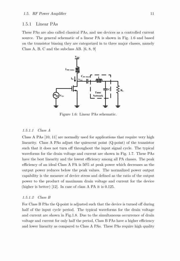
This chapter focuses on the different variants of pulse-width modulation basedtransmitters used for the amplification of non-constant envelope signals. First,the Radio-Frequency Pulse-Width Modulation Transmitter (RF-PWMT) isdiscussed, which requires small chip area and does not suffer from spectralregrowth. Next, the polar PWM transmitters (PPWMT), also known as theburst mode transmitter or the carrier based PWM transmitter, are discussed.PPWMT have a better performance characteristics at high frequency and canuse either SMPAs or linear PAs operating at saturation power.
3.1 Radio-Frequency PWM TransmitterThe radio-frequency pulse-width modulated transmitter (RF-PWMT) [48–51,51–56] varies the transmitted signal amplitude and phase by varying the widthand position of the RF pulse train at a frequency equal to the carrier frequency.Unlike outphasing, the RF-PWMT requires smaller chip area since the combineris not required [57]. Also there is no spectral regrowth due to mismatch [32, 58].
The block diagram of the transmitter is shown in Fig. 3.1, where a CORDICprocessor [59] splits the baseband signal into its phase φ(t) and amplitude a(t)components. The phase component varies the pulse position of a pulse train togenerate the pulse-position modulated (PPM) signal, given in (3.1) [60], wherethe pulse-repetition frequency of a pulse train is equal to the carrier frequency.The amplitude component is first pre-distorted according to (3.2), then thepre-distorted amplitude is used to vary the pulse width of the PPM signal
27

28 Chapter 3.
CORDIC
a(t)
φ(t)
I
QPulse
Position
Mod.
RF-PWM
RLoad
BPF
SMPA
Figure 3.1: Block diagram of an RF-PWM transmitter.
to generate a pulse-width and position-modulated (PWPM) signal, given in(3.3) [50]. The PWPM signal has a constant-envelope and is amplified by anSMPA and finally band-pass filtered to generate a non-constant envelope signalfor transmission.
vPPM (t) = 12 + 2
πcos(ωct+ 2πTP (t)
Tc
)+∞∑k=2
2kπ
sin(kπ
2
)cos(kωct+ 2kπTP (t)
Tc
) (3.1)
where
TP (t) = φ(t)Tc2π
a′(t) = 1π
sin−1 (a(t)) (3.2)
vPWPM = a′(t)+ 2πa(t) cos
(ωct+ 2πTP (t)
Tc
)+∞∑k=2
2kπ
sin (ka′(t)) cos(kωct+ 2kπTP
Tc
) (3.3)
However, this transmitter has a small dynamic range at high carrier frequency,as narrow pulses are swallowed by either the driver chain or the SMPA due totheir finite switching frequency [48]. Multilevel RF-PWM [61] can be used toaddress the problem of small dynamic range at the increased cost of several PAsand a combiner.
3.2. Polar PWM Transmitter 29
3.2 Polar PWM Transmitter
3.2.1 Concept
The polar PWM transmitter (PPWMT) [62–65] have a larger dynamic range athigh carrier frequency as it does not suffer from pulse swallowing in PAs [48].In the PPWMT, the non-constant envelope signal is converted into carrierbursts of varying duration, which operate the PA in either on state achievingpeak efficiency or the off state where no power consumed. These carrier burstsafter amplification are band-pass filtered to generate an amplified non-constantenvelope signal.
Band Pass Filter
RLoad
Phase Modulator
Component Separator Linear PA
orSMPA
φ(t)
a(t)
PWM
xPWM(t)
c(t)
xCPWM-PA(t)or
xCPWM-SMPA(t)
x(t)
ωC
ωIF
Figure 3.2: Block diagram of a polar PWM transmitter.
The block diagram of a PPWMT is shown in Fig. 3.2, which separatethe baseband signal x(t) given in (3.4), to its amplitude a(t) and phase φ(t)components.
x(t) = a(t)ejφ(t) (3.4)
The amplitude component (a(t)) varies the pulse width of pulse train to gener-ate a PWM signal having pulse-repetition frequency (PRF) equal to intermediatefrequency [60, 66], which is expressed as
xPWM = τ(t)T
+∞∑k=1
2kπ
sin(kπτ(t)T
)cos(ωIF kt) (3.5)
where τ is the pulse width, T is the pulse-repetition period (PRP), k is theharmonic number and ωIF is the PRF of the PWM signal. The relationship

30 Chapter 3.
between a(t) and τ is given as
τ(t) = a(t)T. (3.6)
The pulse-width modulation of the pulse train with respect to a(t) is shown inFig. 3.3(b).
The phase component varies the phase of the carrier to generate the phase-modulated carrier, given as
c(t) = cos (ωct+ φ(t)) . (3.7)
Fig. 3.3(d) illustrates the phase modulation of the carrier with respect to φ(t).The phase-modulated carrier is then multiplied by the PWM signal to produce
the carrier-based PWM signal (C-PWM), which is shown in Fig. 3.3(e) andmathematically expressed as
xCPWM =(τ(t)T
+∞∑k=1
2kπ
sin(kπτ(t)T
)cos(ωIF kt)
)cos (ωct+ φ(t)) . (3.8)
The C-PWM signal is then amplified by an SMPA or linear PA and finallyfiltered to generate an amplified non-constant envelope transmitted signal, whichis shown in Fig. 3.3(f).
3.2.2 Efficiency
In general, the transmitter efficiency is defined as the ratio of the transmittedsignal power to the dc power consumed by the transmitter, which is given in(3.9) for constant input signal x(t) = a, where a ∈ [0, 1], η is the efficiency ofthe transmitter, PT is the transmitted signal power and PdcT is the dc powerconsumed by the transmitter [67].
η(a) = PT (a)PdcT (a) (3.9)
In a transmitter the major power is consumed by the PA and the followingpassive circuitry, hence a simplified expression of transmitter efficiency is theratio of the transmitted signal power to the power consumed by the PA [67–69]and is given as
η(a) = PT (a)PdcPA(a) (3.10)
where PDCPA is the power consumed by the PA. This implies that the efficiencyof the PPWMT can be expressed as the product of the PA efficiency and the

3.2. Polar PWM Transmitter 31
0 5 10 15 20 25 30 35 40 45 500
0.5
1
Time (nsec)
Am
p(a)
0 5 10 15 20 25 30 35 40 45 500
0.5
1
Time (nsec)
Am
p
(b)
0 5 10 15 20 25 30 35 40 45 500
2
4
Time (nsec)
Ph
ase
(c)
0 5 10 15 20 25 30 35 40 45 50−1
0
1
Time (nsec)
Am
p
(d)
0 5 10 15 20 25 30 35 40 45 50−1
0
1
Time (nsec)
Am
p
(e)
0 5 10 15 20 25 30 35 40 45 50−1
0
1
Time (nsec)
Am
p
(f)
Figure 3.3: (a) Baseband amplitude component, (b) pulse-width modulationof the pulse train, (c) baseband phase component, (d) phase modulation ofthe carrier, (e) the carrier-based PWM signal, (f) the non-constant envelopetransmitted signal.

32 Chapter 3.
coding efficiency [68, 69], given as
η(a) = ηPA(a)ηC(a) (3.11)
where ηPA is the efficiency of the PA and ηC is the coding efficiency which isthe measure of the reflected power absorbed by the isolator.
In the PPWMT, the PA remains on for a duration τ while it is off forduration (T − τ) during a pulse-repetition period T . Hence, the PA efficiencyfor a constant amplitude a is the average efficiency of the PA determined overthe pulse-repetition period T , which is given as
ηPA(A) = PONτ
PDCON τ + PDCOFF (T − τ) (3.12)
where PON and PDCON is the output power and the power consumed by thePA when it is on, respectively, and PDCOFF is the power consumed by the PAwhen it is OFF. Ideally for Class B/C PAs and SMPAs, there is a peak efficiencywhen PA is ON and there is no power consumption when the PA is OFF, hence(3.12) can be modified as
ηPA = PONPDCON
= ηPA(Peak). (3.13)
The coding efficiency is the ratio of the transmitted signal power to theCPWM signal power at the PA output. For a constant input signal the codingefficiency is given as
ηC(a) = PT (a)PCPWM (a) (3.14)
where PCPWM (a) is the power of the CPWM signal for a constant input signal.The RF transmitted signal for a constant input signal is given as
xT (t) = a cos(ωct). (3.15)
Assuming the carrier frequency ωc is much higher than the PWM frequencyωIF , then the transmitted signal power for a normalized load of 1 Ω can beapproximated as [68]
PT (a) = 1T
∫ T
0x2T (t)dt = 1
2 a2. (3.16)
Fig. 3.4 shows the CPWM signal for a constant input signal, which is thecombination of carrier burst of duration τ(a) and zero signal of duration (T−τ(a)).

3.2. Polar PWM Transmitter 33
T − τ(a)τ(a)
T
Figure 3.4: CPWM signal for a constant input a = τ(a)/T .
It repeats after a period T , hence the power for a normalized load of 1 Ω can becalculated as [68]
PT (a) = 1T
∫ T
0(cos(ωct))2
dt = 12 a. (3.17)
The coding efficiency expression in terms of a constant input signal is obtainedby substituting (3.16) and (3.17) into (3.14), which is given as
ηC(a) =12 a
2
12 a
= a. (3.18)
The efficiency of the PPWMT for an ideal SMPA and class B PA is shown inFig. 3.5, which shows a variation in efficiency with respect to input amplitude.
3.2.3 Polar PWT Transmitter Issue
The issues that need to be considered when using the PPWMT are the band-passfiltering requirements, the image distortion [70], the amplitude aliasing distortionand the phase aliasing distortion [65]. The last two issues are related to thedigital implementation of the PWM and phase modulator.
3.2.3.1 Band-Pass Filtering Requirement
As discussed in Section 3.2.1, the PPWMT converts the amplitude componentto a PWM signal. The spectrum of the PWM signal is determined by taking a

34 Chapter 3.
0.1 0.2 0.3 0.4 0.5 0.6 0.7 0.8 0.9 10
0.1
0.2
0.3
0.4
0.5
0.6
0.7
0.8
0.9
1
Amplitude
Eff
icie
ncy
Ideal SMPAIdeal Class B
Figure 3.5: Efficiency of the PPWMT for an ideal SMPA and a Class B PA.
Fourier transform of (3.5) [60, 65], and is given as
XPWM (ω) = A(ω)
+∞∑k=0
∞∑l=0
2(−1)l(πk)2l
(2l + 1)! × π [A2l+1(ω + kωIF ) +A2l+1(ω − kωIF )]
(3.19)
where A(ω) = Fa(t), Al(ω) = Fal(t) and F. denote the Fourier transform.The plot of (3.19) is shown in Fig. 3.6 for ω = 2π×200Mrad/sec (200MHz). Itcan be observed from the spectrum there is a desired amplitude component at DCand infinite harmonic components at both negative and positive multiples of ωIF ,which is shifted to the carrier frequency ωc after up-conversion. The band-passfilter suppress all the harmonic components of the up-converted PWM signalto achieve the desired transmitted signal, hence band-pass filtering requirementdepends on ωIF , i.e. smaller value of ωIF results more stringent band-passfiltering requirements and vice versa. However, a higher the value of ωIF leadsto a smaller dynamic range due to low amplitude resolution, image distortionand amplitude aliasing distortion.
3.2.3.2 Image Distortion
Image distortion [70] occurs due to the infinite spectrum of the PWM signal,which leads to a lower dynamic range and amplitude non-linearity.

3.2. Polar PWM Transmitter 35
−2 −1.5 −1.0 −0.5 0 0.5 1.0 1.5 2.00
0.1
0.2
0.3
0.4
0.5
0.6
0.7
0.8
0.9
1
Frequency (GHz)
Nor
mal
ized
Am
plit
ude
Figure 3.6: Spectrum of a PWM signal.
−3 −2 −1 0 1 2 30
0.05
0.1
0.15
0.2
0.25
0.3
0.35
0.4
0.45
0.5
Frequency (GHz)
Nor
mal
ized
Am
plitu
de
+fc Spectrum
−fc Spectrum
Figure 3.7: Spectrum of a CPWM signal.

36 Chapter 3.
As discussed in Section 3.2.1, the CPWM signal is generated by multiplicationof the PWM signal and the phase-modulated carrier, which is given in (3.5). Thespectrum of (3.5) is shown in Fig. 3.7 for ωIF = 2π× 200Mrad/sec (200MHz),ωc = 2π Grad/sec (1GHz), a = 0.5 and φ = 0. It is evident from Fig. 3.7 thatthe spectrum of the PWM signal is shifted to ±ωc. As the PWM spectrum hasinfinite harmonic components this causes an intersection of both the shiftedPWM spectrums. This leads to an overlap of transmitted signal and kth harmoniccomponent of shifted PWM signal resulting in a distortion referred as imagedistortion.
The CPWM signal can be amplified by either a linear PA or SMPA. In caseof amplification by a linear PA, there is no increase in image distortion. However,in case of the SMPA, the image distortion is increased compared to the CPWMsignal, as the SMPA converts the sinusoid carrier bursts to the square-wavecarrier bursts. The expression for square-wave carrier bursts is given as
xSMPA(t) =(τ(t)T
+∞∑k=1
2kπ
sin(kπτ(t)T
)cos(ωIF kt)
)(
12 + 2
πcos (ωct+ φ(t)) +
∞∑m=2
2qπ
sin(qπ
2
)cos (qωct+ qφ(t))
).
(3.20)
The plot of (3.20) and its spectrum is shown in Fig. 3.8 for ωIF = 2π ×200Mrad/sec (200MHz) and ωc = 2π Grad/sec (1GHz). The spectrum plotshows multiple attenuated PWM spectra at ±qωc (q = 0, 1, 2, ...,∞), hence qharmonic components exist along with the transmitted signal, which results inhigher image distortion.
3.2.3.3 Amplitude Aliasing Distortion
The amplitude aliasing distortion [65, 71] is due to the digital implementationof the pulse-width modulator. The digital PWM signal is a sampled versionof the analog PWM signal, hence the rising and falling edges occur only atinteger multiples of the sampling period. The digital PWM signal and itsspectrum [71, 72] are given as
xPWM (nTs) =(τ(nTs)T
+∞∑k=1
2kπ
sin(kπτ(nTs)
T
)cos(ωIF knTs)
)(3.21)
XPWM
(ejω)
= 1Ts
∞∑ρ=−∞
XPWM
(j
(ω
Ts− 2πρ
Ts
))(3.22)

3.2. Polar PWM Transmitter 37
−4 −3 −2 −1 0 1 2 3 40
0.1
0.2
0.3
0.4
0.5
Frequency(GHz)
Nor
mal
ized
Am
plitu
de
(b)
+fc Spectrum
dc Spectrum−f
c Spectrum
+3fc Spectrum
−3fc Spectrm
1.6 1.8 2 2.2 2.4 2.6
x 10−8
0
0.2
0.4
0.6
0.8
1
Time(Sec)
Nor
mal
ized
Am
plitu
de
(a)
Figure 3.8: (a) The CPWM signal amplified by a SMPA, (b) spectrum of theCPWM signal amplified by a SMPA

38 Chapter 3.
where n is the sampling index and Ts is the sampling period. The plot of thedigital PWM and its spectrum is shown in Fig. 3.9 for ωIF = 2π × 200Mrad/s
(200MHz) and ωs = 2π Grad/s (1GHz). The spectrum shows the repetitionof the analog PWM spectra at ±nωs (n = 0, 1, 2, ...,∞), which results in analiasing in the baseband amplitude component due to the harmonic componentof the PWM spectra at ±nωs. This distortion is referred to as amplitude aliasingdistortion of the transmitted signal.
This distortion contributes to lowering the dynamic range and increasing theamplitude non-linearity of the system.
3.2.3.4 Phase Aliasing Distortion
The phase aliasing distortion [65] is due to the digital implementation of thephase modulator, which causes phase non-linearity in the transmitter.
In the digital domain, the phase modulation is achieved by pulse-positionmodulation (PPM), which can be implemented as a sampled-based system or bysynchronous delay lines. In both cases, the time resolution of the PPM is limitedby the sampling clock frequency or by the unit delay of the delay lines. As aresult, the number of phases of the digital PPM are also limited and is given as
Nφ = ωresωc
(3.23)
where Nφ is the total number of phases, ωres = 1/2πTres is the samplingfrequency in case of sample-based system, or the inverse of the unit delay incase of delay line, and ωc = 1/2πTc is the carrier frequency.
The effect of limited time resolution can also be explained from the spectrumof the digital PPM signal. The digital PPM signal and its spectrum [72] aregiven as
xPPM (nTs) = 12 + 2
lπcos (ωcnTs + φ(nTS))
+∞∑m=2
2lπ
sin(lπ
2
)cos (lωcnTs + lφ(nTs))
(3.24)
XPPM (ejω) = 1Tres
∞∑ρ=−∞
CPPM
(j
(ω
Tres− 2πρTres
))(3.25)
The (3.25) shows the repetition of analog PPM spectra at integer multiple of ωres.The spectrum of the analog PPM has infinite components which cause aliasingin the phase-modulated carrier and is referred to as phase-aliasing distortion.

3.2. Polar PWM Transmitter 39
0 0.1 0.2 0.3 0.4 0.5 0.6 0.7 0.8 0.9 1
x 10−8
−0.5
0
0.5
1
1.5
Time
Nor
mal
ized
Am
plitu
de
(a)
−3 −2 −1 0 1 2 30
0.2
0.4
0.6
0.8
1
Frequency (GHz)
Nor
mal
ized
Am
plitu
de
(b)
BB Spectrum+f
s Spectrum
−fs Spectrum
+2fs Spectrum
−2fs Spectrum
Figure 3.9: (a) Digital PWM signal in time domain, (b) digital PWM spectrum.


Chapter 4
Polar PWM Transmitters with Reduce Imageand Aliasing Distortion
Chapter 3 discussed the image, amplitude aliasing and phase aliasing distortionsof the PPWMT. The image distortion is due to the up-conversion of the PWMsignal to the carrier frequency. The amplitude aliasing distortion occurs due tothe digital implementation of the pulse-width modulator and the phase aliasingdistortion is due to the digital implementation of the phase modulator. Thesedistortions result in a lower dynamic range of the transmitter and also causenon-linearity in the amplitude and phase of the transmitted signal. The focus ofthis chapter is on variants of PPWMT that either compensate or eliminate theimage and aliasing distortions.
The outline of this chapter is as follows: The first section discusses image-distortion free PPWMTs. In the second section, the aliasing-free PWM trans-mitter (AF-PWMT), its efficiency and problems are discussed. The third sectionbriefly discusses the novel combined RF and AF-PWM transmitter (CRFAF-PWMT) presented in Paper A. In the fourth section, the aliasing-compensatedPWM transmitter (AC-PWMT) presented in Paper B and Paper C is brieflydiscussed. The fifth section presents the simulated performance of PPWMT, AF-PWMT, CRFAF-PWMT and AC-PWMT. Finally, the enhanced phase-resolutionpolar PWM transmitter (EP-PPWMT) of Paper D is briefly discussed.
41

42 Chapter 4.
4.1 Image-Distortion Free Polar PWM Transmitter
The image distortion in the polar PWM transmitter can be eliminated or reducedby exploiting the image gap between the transmitted signal and the adjacentharmonics or by the elimination of image harmonic components that distort thetransmitted signal.
4.1.1 Exploiting Image Gap
The image distortion of the PPWMT can be eliminated or reduced by selectingthe PWM frequency (ωIF ) with respect to the carrier frequency (ωc), such thatnone of the harmonic components of image PWM signal occurs in the transmittedsignal band. Instead the image harmonic components occur in frequency bandsinbetween the transmitted signal and the adjacent harmonics [70]. Fig. 4.1ashows the spectrum of an up-converted PWM signal with an image distortion dueto improper selection of ωIF , whereas the spectrum with no image distortion dueto the proper selection of ωIF is shown in Fig. 4.1b. This technique eliminatesthe image distortion in case of a linear PA. However, in case of an SMPA,the image distortion is only reduced and not completely eliminated. Althougheffective, this technique requires strict bandpass filtering to achieve the desiredresults.
4.1.2 Elimination of Image Distortion
An alternative approach is to quantize the amplitude component a(t) of thebaseband signal such that the harmonic components of the image PWM spectrumlocated in the transmitted signal band are eliminated [70]. Although thistechnique overcomes the image distortion, it results in a higher quantizationnoise.The steps to eliminate the image harmonics distorting the transmitted signalare as follows:
1. Determine the order of the highest amplitude image harmonic componentlocated in the transmitted signal band. In the case of a linear PA ordifferential SMPAs, the order of the image harmonic component in thetransmitted signal band is determined as
q = round
(2ωcωIF
). (4.1)

4.1. Image-Distortion Free Polar PWM Transmitter 43
−4 −2 0 2 40
0.1
0.2
0.3
0.4
0.5
Frequency (GHz)
Nor
mal
ized
Am
plitu
de
(a)
−4 −2 0 2 40
0.1
0.2
0.3
0.4
0.5
Frequency (GHz)
Nor
mal
ized
Am
plitu
de
(b)
+fc Spectrum
−fc Spectrum
+fc Spectrum
−fc Spectrum
Figure 4.1: Spectra of the up-converted PWM signal (a) image distortion dueto improper selection of ωIF , (b) no image distortion due to proper selection ofωIF .

44 Chapter 4.
Whereas in the case of a single ended SMPA, it is determined as
q = round
(ωcωIF
). (4.2)
2. Quantize the amplitude component according to following expression
â = ∆q.round
(a (t)∆q
)(4.3)
where ∆q = 1/q is the the quantize interval parameter.
Band-Pass Filter
RLoad
Phase Modulator
CORDIC
PA
φ(t)
a(t)I
Q
Band-LimitedPWM
Figure 4.2: Block diagram of the aliasing-free PWM transmitter.
4.2 Aliasing-Free PWM Transmitter
4.2.1 Concept
The aliasing-Free PWM transmitter [71, 73–75] (AF-PWMT) eliminates thealiasing and image distortion by limiting the number of harmonics of the digitalPWM signal.
The block diagram of the AF-PWMT is shown in Fig. 4.2. The transmitterseparates the baseband signal x(t) into its amplitude a(t) and phase φ(t) com-ponents. The amplitude component generates a digital PWM signal with finiteharmonic components, hereafter referred to as a band-limited PWM (BL-PWM)signal [71], which is given as
xBL−PWM (nTs) = τ (nTs)T
+K∑k=1
2kπ
sin(kπτ (nTs)
T
)cos (ωIF knTs) (4.4)

4.2. Aliasing-Free PWM Transmitter 45
0 10 20 30 40 0 10 20 30 40 0−0.2
0
0.2
0.4
0.6
0.8
1
1.2
Time(ns)
Am
plitu
de
(a)
−4 −2 0 2 4 1 2 3 40
0.2
0.4
0.6
0.8
1
Frequency (GHz)
Nor
mal
ized
Am
plitu
de
(b)
BB−Spectrum
+fs Spectrum
−fs Spectrum
+2fs Spectrum
−2fs Spectrum
Figure 4.3: (a) BL-PWM signal, (b) BL-PWM spectrum.

46 Chapter 4.
where τ(nTS) = a(nTS)T , a(nTS) is the baseband signal amplitude at instancenTS and K is the total number of harmonics in the BL-PWM signal. In orderto eliminate the aliasing and image distortions, K must ensure the followingconditions
KωIF < 2π/TsKωIF < ωc
. (4.5)
The BL-PWM signal and its spectrum is shown in Fig. 4.3. This BL-PWMsignal is then converted into an analog signal using a digital-to-analog convertor(DAC), which is given as
xBL−PWM (t) = τ (t)T
+K∑k=1
2kπ
sin(kπτ (t)T
)cos (ωIF kt) . (4.6)
The phase component φ(t) varies the phase of the carrier to generate aphase-modulated carrier, which is multiplied by the xBL−PWM (t) to generate acarrier-based BL-PWM (CBL-PWM) signal expressed as
xCBL−PWM (t) = τ (t)T
cos (ωct+ φ (t))
+(
K∑k=1
2kπ
sin(kπτ (t)T
)cos (ωIF kt)
)cos (ωct+ φ (t)) .
(4.7)
The CBL-PWM signal and its spectrum is show in Fig. 4.4. This signal isamplified by the PA and finally filtered to generate the transmitted signal.
The major disadvantage of the AF-PWMT is that it can only use a linearPA operating at low efficiency for the amplification of the CBL-PWM signal.
4.2.2 Efficiency
As discussed in chapter 3 the major power consumption in transmitter is due tothe PA and the following passive circuitry, which implies that the efficiency ofthe AF-PWMT is the product of the PA efficiency and the coding efficiency [68],mathematically expressed as
η(A) = ηPA(a, k)ηc(a). (4.8)
As discussed earlier, the AF-PWMT converts the amplitude a of the basebandinput into a variable amplitude BL-PWM signal, which is mixed with a phase-modulated carrier to generate a non-constant envelope CBL-PWM signal. Since

4.2. Aliasing-Free PWM Transmitter 47
−5 −4 −3 −2 −1 0 1 2 3 4 50
0.1
0.2
0.3
0.4
0.5
Frequency (GHz)
Am
plitu
de
(b)
+fc Spectrum
−fc Spectrum
0 5 10 15 20 25 30−1
−0.5
0
0.5
1
Time(ns)
Am
plitu
de
(a)
Figure 4.4: . (a) CBL-PWM signal, (b) CBL-PWM spectrum.

48 Chapter 4.
the PA efficiency varies with the envelope of the CBL-PWM, hence ηPA is theaverage efficiency, which in case of an ideal class B PA is given as [76, 77]
ηPA = π
4Ex2
BL−PWMExBL−PWM
. (4.9)
The coding efficiency in case of an AF-PWMT is defined as [69]
ηc(a) = PT (a)PCBL−PWM (a) (4.10)
where PT (a) is the power of the RF transmitted signal and PCBL−PWM is thepower of the CBL-PWM signal at the PA output. The PT (a) for a normalizedload of 1 Ω is approximated in section 3.2 and is given as
PT (a) = 12a
2. (4.11)
The PCBL−PWM for a normalized load of 1 Ω is given as
PCBL−PWM = 1T
∫ T
0x2CBL−PWM (t)dt
= 1T
∫ T
0
(τ(a)T
+K∑k=1
2kπ
sin(kπτ(a)T
)cos(ωIF kt)
)2
cos2(ωct)
= 12a
2 + 1T
∫ T
0
(K∑k=1
2kπ
sin(kπτ(a)T
)cos(ωIF kt)
)2
cos2(ωct).
(4.12)
Substituting the value PT (a) and PCBL−PWM (a) into (4.10), the completeexpression for the coding efficiency is given as
ηC(a, k) =12a
2
12a
2 + 1T
∫ T0
(∑Kk=1
2kπ sin
(kπτ(a)T
)cos(ωIF kt)
)2cos2(ωct)
. (4.13)
Equation (4.13) can be simplified as [69]
ηC(a, k) ≈ 11 + 2
∑Kk=1 sinc
2(kA). (4.14)
Substituting the value of ηPA given in (4.9) and ηC(a, k) given in (4.14) into(4.8) gives the complete expression for the efficiency of the AF-PWMT, which is
η(a, k) = π
4Ex2
BL−PWMExBL−PWM
(1
1 + 2∑Kk=1 sinc
2(kA)
). (4.15)
The plots for the theoretical efficiency of the AF-PWMT for an ideal class B PAgiven in Fig. 4.5.

4.3. Combined RF and AF-PWM Transmitter 49
−20 −18 −16 −14 −12 −10 −8 −6 −4 −2 00
0.1
0.2
0.3
0.4
0.5
0.6
0.7
0.8
Normalized Output Power (dB)
Effi
cien
cy
Figure 4.5: The theoretical efficiency of AF-PWMT for ideal class B PA.
4.3 Combined RF and AF-PWM Transmitter
The Combined RF and AF-PWM Transmitter (CRFAF-PWMT) is the contri-bution of Paper A. This section briefly discusses the CRFAF-PWMT alongwith a comparison of theoretical instantaneous efficiency of the AF-PWMT andthe CRFAF-PWMT. The detail concept, analog and digital implementations,efficiency analysis and measurement results are given in Paper A.
This transmitter eliminates the amplitude aliasing and image distortion inthe transmitted signal while achieving a high power efficiency as it uses an SMPAfor amplification. The advantages of this transmitter over the AF-PWMT ishigher power efficiency and its implementation by all-digital circuits. Fig. 4.6shows the comparison of the instantaneous efficiency for the CRFAF-PWMTusing an ideal SMPA (i.e. no loss in switching and impedance matching networkfor all duty cycles) and AF-PWMT using an ideal class B PA.
The block diagram of the CRFAF-PWMT is shown in Fig. 4.7, which sepa-rates the baseband signal into phase (φ(nTs)) and amplitude components(a(nTs)).The φ(nTs) generates the pulse-position modulated signal by varying the pulseposition of a pulse train having a frequency equal to the carrier frequency. Thea(nTs) generates a BL-PWM signal with a repetition frequency equal to theintermediate frequency. This BL-PWM signal varies the pulse width of the

50 Chapter 4.
−20 −18 −16 −14 −12 −10 −8 −6 −4 −2 00
0.1
0.2
0.3
0.4
0.5
0.6
0.7
0.8
0.9
1
Normalized Output Power (dB)
Effi
cien
cy
CRFAF−PWMT
AF−PWMT
Figure 4.6: The theoretical efficiency of the AF-PWMT and CRFAF-PPWMT.
Filter
RLoad
Pulse-Position
Modulator
ComponentSeparator
SMPAφ
aBL-PWM
RF-PWMx
xBL-PWM
ωC
vRF-PPM
Pre-Dist.V’BP
VRF-BLPWM
Figure 4.7: Block diagram of the combined RF aliasing-free PWM transmitter.
4.4. Aliasing-Compensated PWM Transmitter 51
pulse-position modulated signal to generate a constant envelope band-limitedRF-PWM signal, which is amplified by an SMPA and finally filtered to generatea distortion-free transmitted signal.
4.4 Aliasing-Compensated PWM Transmitter
The aliasing-compensated PWM transmitter(AC-PWMT) and its all-digitalimplementation are the contribution of the Paper B and Paper C. Paper Bgives a detailed discussion on the AC-PWMT along with its efficiency analysis,whereas Paper C gives the all-digital implementation.
This transmitter compensates for amplitude aliasing and image distortion inthe transmitted signal by combining the two outphasing PWM signals after thefinal amplification. The advantage of this transmitter over the AF-PWMT isa higher efficiency as it allows the use of both SMPAs or linear PAs operatingat saturation power. The curve for the theoretical efficiency of the AC-PWMTusing an ideal SMPA and a class B PA is shown in Fig. 4.8. The figure alsoshows the theoretical efficiency of the AF-PWMT using an ideal class B PA forcomparison.
−20 −18 −16 −14 −12 −10 −8 −6 −4 −2 00
0.1
0.2
0.3
0.4
0.5
0.6
0.7
0.8
0.9
1
Normalized Output Power (dB)
Effi
cien
cy
AC−PWMT SMPA
AC−PWMT Class B PA
AF−PWMT
Figure 4.8: The theoretical efficiency of AC-PWMT (for SMPA and class B PA)and AF-PWMT.

52 Chapter 4.
RL
C
O
R
D
I
C
Quant PWM
Outphasing Combiner Isolator Filter
fc
V2
V1 V1PWM
V2PWM
e(nTs)
a’(nTs)a(nTs)
φ(nTs)
x(nTs)
xPWM
PA
PA
÷ VPWM
Figure 4.9: Block diagram of the AC-PWMT.
The block diagram of the AC-PWMT is shown in Fig. 4.9, which separatesthe baseband signal into its amplitude a(nTS) and phase φ(nTS) components.a(nTS) is then quantized to a′(nTS), which generates an aliasing-free PWM signalXPWM . The error ratio e(nTS) due to quantization is added and subtracted tothe phase component φ(nTS) to generate two outphasing angles. The carrieris then phase modulated according to the outphasing angles to generate twooutphasing carriers which are multiplied by XPWM to generate two carrier-basedPWM signals. These carrier-based PWM signals are amplified by PAs, thencombined and finally filtered to generate the aliasing and image distortion freetransmitted signal.
4.5 Simulation Results
This section presents the performance of the PPWMT, AF-PWMT, CRFAF-PPWMT and AC-PWMT. The simulations are done using Cadence and ADSusing a standard 130 nm CMOS technology for a carrier frequency of 1 GHz.The PPWMT and CRFAF-PWMT are simulated using a 1 Watt class D PA,the AF-PWMT using a 1 Watt class AB PA and the AC-PWMT using a pair of0.5 watt class D PAs.
The amplitude linearity of the transmitters is shown in Fig. 4.10, where thenormalized output amplitude is plotted against the normalized input amplitude.It can be observed that the PPWMT has a staircase-like characteristics due tothe aliasing distortion of the pulse-width modulator. The AF-PWMT and theCRFAF-PWMT show a near linear behavior, with the CRFAF-PWMT showinga better linearity. The distortion in amplitude linearity of AF-PWMT is due tothe AM-AM distortion of the class AB PA, whereas for the CRAF-PPWMT it isdue to the limited switching speed of the MOS devices. Finally, the AC-PWMT

4.5. Simulation Results 53
0.1 0.2 0.3 0.4 0.5 0.6 0.7 0.8 0.9 10
0.1
0.2
0.3
0.4
0.5
0.6
0.7
0.8
0.9
1
Normalized Input Amplitude
Nor
mal
ized
Out
put A
mpl
itude
PPWMTCRFAF−PWMTAF−PWMTAC−PWMT
Figure 4.10: Amplitude linearity plot of the PPWMT, CRFAF-PPWMR, AF-PWMT and AC-PWMT.
−20 −18 −16 −14 −12 −10 −8 −6 −4 −2 00
0.1
0.2
0.3
0.4
0.5
0.6
0.7
Normalized Output Power (dB)
Effi
cenc
y
PPWMTCRFAF−PWMTAF−PWMTAC−PWMT
Figure 4.11: Instantaneous efficiency plot of the PPWMT, CRFAF-PWMT,AF-PWMT and AC-PWMT.

54 Chapter 4.
Table 4.1: Specification and performance of PPWMT, AF-PWMT, CRFAF-PWMT and AC-PWMT
PPWMT AF-PWMT CRFAF-PWMT AC-PWMTDynamic
28 dB 33.4 dB 45 dB 35 dBRangeAverage
33% 8.3% 34% 31.5%EfficiencyPAType Class D Class AB Class D Class D
Quantity 1 1 1 2Peak Power 30 dBm 30 dBm 30 dBm 27 dBm
Peak69% 60% 69% 69%Efficiency
Carrier1 GHz 1 GHz 1 GHz 1 GHzFrequency
Baseband LTE-UL LTE-UL LTE-UL LTE-ULInput 1.4 MHz 1.4 MHz 1.4 MHz 1.4 MHz
shows the best linearity among all the compared transmitters.The instantaneous efficiency of the transmitters is shown in Fig. 4.11. The
CRFAF-PWMT outperforms the other transmitters, whereas the AC-PWMThas a better efficiency compared to the AF-PWMT.
Table 4.1 shows the performance of the PPWMT, AF-PWMT, CRAF-PWMTand AC-PWMT for a 1.4 MHz LTE up-link signal. It can be seen that theCRFAF-PPWMT has the highest efficiency and dynamic range as compared toall other transmitters. The AC-PWMT has a higher dynamic range and similarefficiency compared to the PPWMT. The AF-PWMT has the lowest efficiencyamong all transmitters.
4.6 Enhanced Phase Resolution All-Digital PWMTrans-mitter
An enhanced phase resolution PWM transmitter (EP-PWMT) is presentedin Paper D. The EP-PWMT increases the phase resolution of an all-digitalPPWMT by using asymmetric outphasing. The limited phase resolution in theall-digital PPWMT is caused by the phase-aliasing distortion due to the digitalphase modulator.

4.6. Enhanced Phase Resolution All-Digital PWM Transmitter 55
CORDIC
Amplitude
Predistortion
Quantization
(2NC)
PWMOutphasing
Position
Phase
Modulator
Phase
Modulator
PAPA
Combiner
Bandpass
Filter
a(nTs)φ (nTs)
φQ (nTs) a’(nTs)
xPWM(nTs)
vT(t)
ψ1(nTs)
ωC
ψ2(nTs)
Baseband Input
Figure 4.12: Block diagram of the EP-PWMT.
The block diagram of the EP-PWMT is shown in Fig. 4.12. It uses aCORDIC to separate the baseband input signal into its phase and amplitudecomponents. The phase component is quantized into 2N levels for a digitalphase modulator of resolution N . Depending on the value of the quantized phase,both phase modulators either generate symmetrical phase-modulated carriers orasymmetrical phase-modulated carriers shifted by the minimum phase resolutionof the phase modulator. The amplitude component is first pre-distorted toovercome the mismatch in the transmitted signal amplitude due to outphasingand then converted into a PWM signal. This PWM signal is then multipliedby phase-modulated carriers to generate carrier-based PWM signals, which arecombined, amplified and then filtered to generate the final transmitted signal.
The simulated performance of the EP-PMWT and the all-digital PPWMT fora class D PAs designed in 130 nm CMOS is shown in table 4.2. The simulationresults show that the EP-PWMT has a better EVM and dynamic range as

56 Chapter 4.
Table 4.2: Performance of the all-digital PPWMT and EP-PWMT.
PPWMT EP-PWMTPeak Power 30 dBm 30 dBm
Average Efficiency 33% 32.8%Dynamic Range 29.8% 33%
EVM 6.9% 3.8%
compared to the all-digital PPWMT, whereas the efficiencies of the transmittersare similar.

Chapter 5
Polar PWM Transmitters withRelaxed Band-Pass Filtering
Chapter 3 discussed the band-pass filtering requirements and the amplituderesolution of the PPWMT. The band-pass filter requirements for the PPWMTare dependent on the PWM pulse-repetition frequency (PRF), i.e., with higherPRF, a more relaxed band-pass filter is required but on the other side thetransmitter has a lower amplitude resolution. This chapter discusses PWMtransmitters that enhance the amplitude resolution while relaxing the band-passfiltering requirements.
The outline of this chapter is as follows: The first section discusses themultilevel PWM transmitter. In the second section, the multiphase PWMtransmitter is discussed. The third section gives a brief overview of the combinedRF and multi-level PWM transmitter (CRF-ML-PWMT) presented in Paper E.The last section discusses the combined RF and multiphase PWM transmitter(CRF-ML-PWMT) presented in Paper F.
5.1 Multi-Level PWM Transmitter
5.1.1 Concept
The multi-level PWM transmitter (ML-PWMT) [68, 69, 78, 79] uses multiplePWM signals in order to improve the amplitude resolution, which results in animproved dynamic range. However, the major issue for the transmitter is the
57

58 Chapter 5.
Combiner & Isolator
Band Pass Filter
RLoad
Phase Modulator
CORDIC
Main SMPA
Auxiliary SMPA
Phase
AmpI
Q
MainPWM
AuxiliaryPWM
Figure 5.1: Block diagram of the 2 level PWM Transmitter.
larger chip area, which is due to the requirement of multiple PAs followed by apower combiner.
The block diagram of a two-level PWM transmitter is shown in Fig. 5.1. Thetransmitter separates the baseband signal x(t) into its amplitude a(t) and phaseφ(t) components. The amplitude component generates two PWM signals. Fora(t) ≤ V1, only the main PWM signal is generated with a duty-cycle proportionalto a(t), whereas for V1 < a(t) ≤ 1 an auxiliary PWM signal is generated alongwith the main PWM signal, such that the duty cycle of the auxiliary PWMis proportional to a(t) − V1 and the main PWM signal has 100% duty cycle.The generation of PWM signals is expressed as (5.1), where V1 is the thresholdvoltage.
xPWMmain = a(t)+V1
∑∞k=1
2kπ sin (kπa(t)/V1) cos(ωIF kt)
xPWMaux= 0
a(t) ≤ V1 (5.1a)
xPWMmain= V1
xPWMaux= (a(t)− V1)+∑∞k=1
2kπ sin (kπ (a(t)− V1)) cos(ωIF kt)
V1 < a(t) ≤ 1 (5.1b)
The phase component φ(t) on the other hand generates a phase-modulatedcarrier, which is multiplied by the PWM signals to generate the main andauxiliary carrier-based PWM (CPWM) signals. These signals are expressed as
xCPWMmain= xPWMmain
× cos (ωct+ φ (t))
xCPWMaux= xPWMaux
× cos (ωct+ φ (t))
. (5.2)

5.1. Multi-Level PWM Transmitter 59
These CPWM signals are amplified by separate PAs and then combined togenerate a two-level composite signal, given as
x2level−CPWM
AxCPWMmain
AxCPWMmain +AxCPWMaux
(5.3)
where A is the gain of PAs. It is evident from (5.3) that the two-level PWMThas twice the amplitude resolution compared to the PPWMT. The two-levelcomposite signal is finally filtered to generate the amplified transmitted signal.
In case of a generalized M-level PWMT, there are M pulse-width modulatedsignals, which are multiplied by a phase-modulated carrier to generate M CPWMsignals. These M CPWM signals are power amplified and combined to generatean M-level composite signal, which is filtered to generate the transmitted signal.The M-level PWMT has an amplitude resolution that is M times that of thePPWMT, however it requires M SMPAs followed by a power combiner.
5.1.2 Efficiency
As discussed in chapter 3 and 4, the major power consumption of a transmitter isdue to the PAs and the circuitry following it, so the efficiency of an ML-PWMTfor a constant input amplitude a is given as
η(a) = ηPA(a)ηcomb(t)ηC(a) (5.4)
where ηPA is the efficiency of PAs, ηcomb is the efficiency of the combiner andηC is the coding efficiency. In case where all the PAs are switch-mode and havethe same efficiency, then ηPA(a) for all amplitudes is given as
ηPA = ηPA(Peak). (5.5)
The ηcomb(a) depends on the type of the combiner. In case of an idealcombiner it is given as
ηcomb(a) = 1. (5.6)
The ηC(a) for the ML-PWMT is the ratio of the transmitted signal power tothe output power at the combiner, hence it depends on the number of PAs used.In case of a two-level PWMT, either only a single PA is operational or both PAsare operational. The coding efficiency when only the main PA is operational isdetermined in a similar manner as the coding efficiency of the PWMT and isexpressed as [68, 70]
ηC1(a) =12a
2
1T
∫ τmain(a)0 (V1 cos (2πfct))2
dt= a
V1∈ (0, V1] (5.7)

60 Chapter 5.
where τmain(a) is the duty cycle of xPWMmain, V1 is its peak amplitude (threshold
voltage) and T is its pulse-repetition period. The relationship between τmain(a)and a is given as
τmain(a) = a
V1T. (5.8)
The coding efficiency, when both main PA and auxiliary PA are operational, isdetermined as follows
ηC1(a) = PT (a)PPWMmain
(a) + PPWMaux(a) . (5.9)
τmain
= T
τaux
Figure 5.2: The waveform at the output of combiner when both main andauxiliary PAs are operational.
Fig. 5.2 shows the waveform at the output of the combiner, when both mainand auxiliary PAs are operational, where τaux is the pulse-width of the xPWMaux
and τmain = T is the pulse-width of the xPWMmain , thus ηC2 (a) is furtherelaborated as [68, 70]
ηC2(a) =12a
2
1T
∫ τaux(a)0 (cos (2πfct))2
dt+ 1T
∫ 1−τaux(a)0 (V1 cos (2πfct))2
dt
= a2
a (V1 + 1)− V1∈ (V1, 1].
(5.10)
The generalized coding efficiency for an M-level PWMT is determined in asimilar manner as the two-level PWMT and it is represented as [68, 70]
ηC(a)
0 for a = 0a2
a(Vm−1+Vm)−Vm−1Vmfor a ∈ (Vm−1, Vm]; m ∈ [1,M ]
(5.11)
where M represents the total number of PWM signals, VM is 1 V and V0 is 0 V .

5.2. Multi-Phase PWM Transmitter 61
Combiner & Isolator
Band Pass Filter
RLoad
Phase Modulator
CORDIC
SMPA 1
SMPA M
Phase
AmpI
Q
0 phasePWM
(M-1)/M phasePWM
Figure 5.3: Block diagram of the M-phase PWM transmitter.
5.2 Multi-Phase PWM Transmitter
5.2.1 Concept
The multi-phase PWM transmitter (MP-PWMT) [80, 81] uses multiple time-shifted PWM signals in order to relax the final band-pass filtering requirementswhile achieving a similar amplitude resolution as the PPWMT. However, likethe ML-PWMT it also requires multiple PAs and a combiner, hence its imple-mentation needs a larger chip area.
The block diagram of the M-phase PWMT is shown in Fig. 5.3. Thetransmitter separates the baseband signal x(t) into phase φ(t) and amplitudea(t) components. The φ(t) generates the phase modulated carrier. The a(t)generates M PWM signals that are time shifted by a factor T/M . The M PWMsignals are expressed as
v1PWM = a(t)M
+∞∑k=1
2Mkπ
sin (kπa(t)) cos (ωIF kt)
v2PWM = a(t)M
+∞∑k=1
2Mkπ
sin (kπa(t)) cos(ωIF kt+ 2kπ
M
)−
−
vMPWM = a(t)M
+∞∑k=1
2Mkπ
sin (kπa(t)) cos(ωIF kt+ 2kπ
M − 1
)
. (5.12)
The M PWM signals are multiplied by the phase-modulated carrier to

62 Chapter 5.
generate M CPWM signals, which are given as
v1CPWM =(a(t)M
+∞∑k=1
2Mkπ
sin (kπa(t)) cos (ωIF kt))
cos (ωct+ φ(t))
v2CPWM =(a(t)M
+∞∑k=1
2Mkπ
sin (kπa(t)) cos(ωIF kt+ 2kπ
M
))cos (ωct+ φ(t))
−
−
vMCPWM =(a(t)M
+∞∑k=1
2Mkπ
sin (kπa(t)) cos(ωIF kt+ 2kπ
M − 1
))cos (ωct+ φ(t))
.
(5.13)The CPWM signals are power amplified and combined to generate the
M-phase CPWM signal (MP-CPWM), which is given as
vMP−CPWM = Aa(t) cos (ωct+ φ (t))
A
M−1∑m=0
∞∑k=1
2Mkπ
sin (kπa(t)) cos(ωIF kt+ 2mkπ
M
)cos (ωct+ φ(t)) .
(5.14)
The transmitter then finally filters the vMP−CPWM to generate the finaltransmitted signal. It is evident from (5.14) the nearest harmonic for the M-Phase PPWMT occurs at M × ωIF , which relaxes the final band-pass filterrequirements as compared to the PPWMT where the nearest harmonic occursat ωIF .
5.2.2 Efficiency
The derivation of efficiency for MP-PWMT is similar to the ML-PWMT, so theefficiency of the multi-phase transmitter is given as
η(a) = ηPA(a)ηcomb(a)ηC(a) (5.15)
where ηPA = ηPA(Peak) for the case of switch-mode PA, ηcomb = 1 for case ofan ideal combiner and ηC is the ratio of the transmitted signal power to thecombiner output power. The coding efficiency for the MP-PPWMT is expressedas
ηC(a) = PT (a)PMP−CPWM (a) =
12a
2
1T
∫ T0 v2
MP−CPWMdt. (5.16)

5.3. Combined RF and ML-PWM Transmitter 63
CORDIC
a(t)
φ(t)
I
QPulse
PositionMod.
RF-PWM
RLoad
BPF
Multi Phase PWM
ClassD PA
Figure 5.4: Block diagram of the CRF-ML-PWMT.
The (5.16) is simplified as [80]
ηC =
a( 1M ) a ∈
(0, 1
M
]a2
a( 1M + 2
M )− 2M2
a ∈( 1M , 2
M
]−−a2
a(M−1M +1)−M−1
M
a ∈(M−1M , 1
]. (5.17)
5.3 Combined RF and ML-PWM Transmitter
The combined RF and ML-PWM transmitter (CRF-ML-PWMT) is the con-tribution of the Paper E. This section briefly discusses the concept of theCRF-ML-PWMT and its simulated efficiency for an ideal SMPA. The detaileddiscussion on the transmitter along with a possible implementation is given inPaper E.
The CRF-ML-PPWMT combines the RF-PWM and ML-PWM to eliminatemultiple PAs and a combiner, hence resulting in a smaller chip area. Thetransmitter also shows a better efficiency compared to the ML-PWMT and alarger dynamic as compared to the RF-PWMT.
The block diagram of CRF-ML-PWMT is shown in Fig. 5.4. The trans-mitter separates the baseband signal into amplitude and phase component.The amplitude component generates the multilevel PWM signal, whereas thephase component generates the pulse-position modulated signal. These pulse-position modulated and multi-level PWM signals are input to the RF pulse-widthmodulator to generate an RF pulse-width and pulse-position modulated sig-

64 Chapter 5.
nal (RF-PWPM), which is amplified by an SMPA and filtered to generate thetransmitted signal.
The simulation results of instantaneous efficiency of the combined RF andthree-level PWM transmitter using an ideal SMPA is shown in Fig. 5.5.
−25 −20 −15 −10 −5 00.1
0.2
0.3
0.4
0.5
0.6
0.7
0.8
0.9
1
Normalized Output Power (dB)
Effi
cenc
y
Figure 5.5: Instantaneous efficiency of the combined RF and three-level PWMtransmitter using an ideal SMPA.
5.4 Combined RF and MP-PWM TransmitterThe combined RF and MP-PWM transmitter(CRF-MP-PWMT) is the con-tribution of the Paper F. This section briefly discusses the concept of thepolar and quadrature CRF-MP-PWMT and its simulated efficiency for an idealSMPA. The detailed description along with mathematical expressions are givenin Paper F.
The CRF-MP-PWMT has a smaller chip area compared to the multiphasePPWMT as it does not require multiple PAs and a combiner. The transmittercombines RF-PWM and multiphase PWM to achieve a larger dynamic range andbetter amplitude resolution at a higher frequency compared to the RF-PWMTand a better efficiency compared to the MP-PWMT.
The block diagram of the polar CRF-MP-PWMT is shown in Fig. 5.6. Thetransmitter first decomposes the baseband signal into phase and amplitudecomponents. The phase component generates the pulse-position modulated

5.4. Combined RF and MP-PWM Transmitter 65
CORDIC
a(t)
φ(t)
I
QPulse
PositionMod.
RF-PWM
RLoad
BPF
Multi Phase PWM
ADDER
ClassD PA
Figure 5.6: Block diagram of the polar CRF-MP-PWMT.
signal. The amplitude component generates the multiphase PWM signals whichare combined to generate the composite signal. This composite PWM signalvaries the pulse width of the pulse-position modulated signal to generate theRF pulse-width and pulse-position modulated signal, which is amplified by anSMPA and filtered to generate the transmitted signal.
The block diagram of the quadrature CRF-MP-PWMT is shown in Fig. 5.7.This architecture decomposes the baseband signal into four components, twopositive components IP and QP , and two negative components IN and QN .These components generate their respective composite signals, which pulse-widthmodulate the time-shifted RF carriers. These pulse-width modulated RF carriershave a maximum pulse width of a quarter of the pulse-repetition period of thecarrier and they are input to a MUX to generate a single combined RF multi-phase PWM carrier signal. This signal is then power amplified by an SMPA andfinally filtered to generate the transmitted signal.
The simulation results of instantaneous efficiency of the combined RF two-phase PWM transmitter using an ideal SMPA is shown in Fig. 5.8.

66 Chapter 5.
SEPARATOR
Multiple PWM
AdderI
Q
RF-PWM
RLoad
BPF
Multiple PWM
Adder RF-PWM
Multiple PWM
Adder RF-PWM
Multiple PWM
Adder RF-PWM
MUX
IP
IN
QP
QN
CLASS DPA
PhaseShifter
Figure 5.7: Block diagram of the quadrature CRF-MP-PWMT.
−25 −20 −15 −10 −5 00.1
0.2
0.3
0.4
0.5
0.6
0.7
0.8
0.9
1
Normalized Output Power (dB)
Effi
cenc
y
Figure 5.8: Instantaneous efficiency of the combined RF and two-phase PWMtransmitter using an ideal SMPA.

Chapter 6
Conclusions and Future Trends
The linearity and efficiency are important parameters in determining the per-formance of wireless transmitters. By using PWM techniques we can make atrade-off between these parameters while allowing all-digital implementation.However, the PWM-based transmitters suffer from aliasing and image distortions.This thesis focuses on techniques to reduce the effects of these distortions bymodifying the architectures of conventional PWM transmitters.
Multiple transmitters have been proposed in this thesis that use PWMalong with other linearization techniques to improve the spectral performancecharacteristics and efficiency. The focus has been to make use of SMPAs,which have a higher efficiency as compared to linear PAs. To emphasize thedigital nature of the proposed architectures, one of the transmitter is completelyimplemented using an FPGA followed by SMPAs for power amplification.
The transmitter proposed in Paper A eliminates amplitude aliasing andimage distortion by combining RF-PWM and band-limited PWM. Class-DSMPAs fabricated in 130 nm CMOS have been used to verify the performanceof the proposed transmitter which shown an improvement of 10.2 dB in thedynamic range.
The PWM transmitters proposed in Paper B and Paper C compensate forthe amplitude aliasing and image distortion due to PWM by using outphasing.The concept is verified using linear PAs in Paper B, whereas in Paper C, anall-digital implementation using an FPGA and Class-D SMPAs is presented.The measurements clearly show an improvement in the linearity of proposedtransmitter as compared to the other PWM based transmitters.
67

68 Chapter 6.
In Paper D, a technique to improve the phase linearity of all-digital PWMbased transmitters is presented. An asymmetric outphasing technique is usedto effectively double the phase resolution. The measurement results show animprovement of 2.8 dB in the adjacent channel leakage ratio with a 3.3%reduction in the EVM.
Paper E and Paper F present area-efficient implementations for multiphaseand multilevel PWM transmitters by eliminating the need for a combiner. Fromthe simulations improvements in dynamic range and efficiency are observed ascompared to conventional PWM transmitters.
For battery-powered wireless devices with multiple transceivers, the linearityand efficiency of the transmitters are important performance parameters. Inrecent years, PWM-based wireless transmitters have been gaining popularitydue to their higher efficiency at the cost of increased distortion. This thesispresents techniques to reduce the distortion in PWM-based transmitters. As thedemand for data rates increase it would be interesting to study the use of PWMtransmitters for simultaneous multi-band transmission. Another interesting areato explore is the feasibility of using PWM based transmitters in the 60 GHzband.

References
69


References
[1] F. Raab, “Radio frequency pulsewidth modulation,” IEEE Trans. Commun.,vol. 21, no. 8, pp. 958–966, Aug 1973.
[2] F. H. Raab, P. Asbeck, S. Cripps, P. B. Kenington, Z. B. Popovic, N. Pothe-cary, J. F. Sevic, and N. O. Sokal, “RF and microwave power amplifier andtransmitter technologies-Part 5,” High Frequency Electronics, pp. 46–54,Jan 2004.
[3] B. Razavi, RF microelectronics, Chapter 4, 2nd ed. Prentice Hall, 2011.
[4] Q. Gu, RF system design of transceivers for wireless communications,Chapter 3. Springer Science & Business Media, 2005.
[5] F. H. Raab, P. Asbeck, S. Cripps, P. B. Kenington, Z. B. Popovic, N. Pothe-cary, J. F. Sevic, and N. O. Sokal, “RF and microwave power amplifier andtransmitter technologies-Part 1,” High Frequency Electronics, vol. 2, no. 3,pp. 22–36, May 2003.
[6] P. A. Dal Fabbro and M. Kayal, Linear CMOS RF Power Amplifiersfor Wireless Applications: Efficiency Enhancement and Frequency-tunableCapability. Springer Science & Business Media, 2010.
[7] A. Raghavan, N. Srirattana, and J. Laskar, Modeling and design techniquesfor RF power amplifiers. John Wiley & Sons, 2008.
[8] T. Johansson and J. Fritzin, “A review of Watt-level CMOS RF poweramplifiers,” IEEE Trans. Microw. Theory Tech., vol. 62, no. 1, pp. 111–124,Jan 2014.
[9] F. H. Raab, P. Asbeck, S. Cripps, P. B. Kenington, Z. B. Popovic, N. Pothe-cary, J. F. Sevic, and N. O. Sokal, “RF and microwave power amplifier andtransmitter technologies-Part 2,” High Frequency Electronics, 2003.
71

72 REFERENCES
[10] S. C. Cripps, RF power amplifiers for wireless communications, Chapter 2.Artech House, 1999.
[11] A. Grebennikov, N. O. Sokal, and M. J. Franco, Switchmode RF andmicrowave power amplifiers, Chapter 1. Academic Press, 2012.
[12] T. H. Lee, The design of CMOS radio-frequency integrated circuits, Chapter13, 1st ed. Cambridge Univ. Press, 1998.
[13] S. C. Cripps, RF power amplifiers for wireless communications, Chapter 6.Artech House, 1999.
[14] A. Afsahi, A. Behzad, and L. E. Larson, “A 65nm CMOS 2.4GHz 31.5dBmpower amplifier with a distributed LC power-combining network and im-proved linearization for WLAN applications,” in Proc. ISSCC, Feb 2010,pp. 452–453.
[15] O. Degani, F. Cossoy, S. Shahaf, D. Chowdhury, C. D. Hull, C. Emanuel,and R. Shmuel, “A 90nm CMOS power amplifier for 802.16e (WiMAX)applications,” in Proc. RFIC, Jun 2009, pp. 373–376.
[16] D. Chowdhury, C. D. Hull, O. B. Degani, Y. Wang, and A. M. Niknejad,“A fully integrated dual-mode highly linear 2.4 GHz CMOS power amplifierfor 4G WiMax applications,” IEEE J. Solid-State Circuits, vol. 44, no. 12,pp. 3393–3402, Dec 2009.
[17] J. Fritzin, C. Svensson, and A. Alvandpour, “Analysis of a 5.5-V class-Dstage used in + 30-dBm outphasing RF PAs in 130 and 65-nm CMOS,”IEEE Trans. Circuits Syst. II, vol. 59, no. 11, pp. 726–730, Nov 2012.
[18] ——, “A +32 dBm 1.85 GHz class-D outphasing RF PA in 130nm CMOSfor WCDMA/LTE,” in Proc. ESSCIRC, Sep 2011, pp. 127–130.
[19] ——, “Design and analysis of a class-d stage with harmonic suppression,”IEEE Trans. Circuits Syst. I, vol. 59, no. 6, pp. 1178–1186, Jun 2012.
[20] S. C. Cripps, RF power amplifiers for wireless communications, Chapter 6.Artech House, 1999.
[21] A. Grebennikov, N. O. Sokal, and M. J. Franco, Switchmode RF andmicrowave power amplifiers, Chapter 2. Academic Press, 2012.

REFERENCES 73
[22] Y. Song, S. Lee, E. Cho, J. Lee, and S. Nam, “A CMOS class-E poweramplifier with voltage stress relief and enhanced efficiency,” IEEE Trans.Microw. Theory Tech., vol. 58, no. 2, pp. 310–317, Feb 2010.
[23] C. Park, D. H. Lee, Y. Lee, J. Han, S. H. Baek, Y. Kim, and S. Hong,“1.8-GHz CMOS power amplifier with stage-convertible structure usingdifferential line inductor,” in Proc. RFIC, Jun 2007, pp. 741–744.
[24] H. Lee, C. Park, and S. Hong, “A quasi-four-pair class-E CMOS RF poweramplifier with an integrated passive device transformer,” IEEE Trans.Microw. Theory Tech., vol. 57, no. 4, pp. 752–759, Apr 2009.
[25] A. Grebennikov, N. O. Sokal, and M. J. Franco, Switchmode RF andmicrowave power amplifiers, Chapter 2. Academic Press, 2012.
[26] S. Moloudi, K. Takinami, M. Youssef, M. Mikhemar, and A. Abidi, “Anoutphasing power amplifier for a software-defined radio transmitter,” inProc. ISSCC, Feb 2008, pp. 568–636.
[27] M. E. Heidari, M. Lee, and A. A. Abidi, “All-digital outphasing modulatorfor a software-defined transmitter,” IEEE J. Solid-State Circuits, vol. 44,no. 4, pp. 1260–1271, Apr 2009.
[28] F. H. Raab, P. Asbeck, S. Cripps, P. B. Kenington, Z. B. Popovic, N. Pothe-cary, J. F. Sevic, and N. O. Sokal, “RF and microwave power amplifier andtransmitter technologies-Part 3,” High Frequency Electronics, pp. 34–48,Sep 2003.
[29] W. B. Sander, S. V. Schell, and B. L. Sander, “Polar modulator for multi-mode cell phones,” in Proc. CICC, Sep 2003, pp. 439–445.
[30] M. R. Elliott, T. Montalvo, B. P. Jeffries, F. Murden, J. Strange, A. Hill,S. Nandipaku, and J. Harrebek, “A polar modulator transmitter forGSM/EDGE,” IEEE J. Solid-State Circuits, vol. 39, no. 12, pp. 2190–2199,Dec 2004.
[31] K. Onizuka, S. Saigusa, and S. Otaka, “A 1.8 GHz linear CMOS power am-plifier with supply-path switching scheme for WCDMA/LTE applications,”in Proc. ISSCC, Feb 2013, pp. 90–91.
[32] B. Razavi, RF microelectronics, Chapter 12, 2nd ed. Prentice Hall, 2011.

74 REFERENCES
[33] H. Chireix, “High power outphasing modulation,” Proc. IRE, vol. 23, no. 11,pp. 1370–1392, Nov 1935.
[34] D. Cox, “Linear amplification with nonlinear components,” IEEE Trans.Commun., vol. 22, no. 12, pp. 1942–1945, Dec 1974.
[35] M. Özen, “Advanced transmitter architectures based on switch mode poweramplifiers,” Ph.D. dissertation, Chalmers University of Technology, 2014.
[36] A. Grebennikov, “Power combiners, impedance transformers and directionalcouplers-Part 1,” High Freq. Electronics, pp. 20–38, Dec 2007.
[37] ——, “Power combiners, impedance transformers and directional couplers-Part 2,” High Freq. Electronics, pp. 42–53, Jan 2008.
[38] ——, “Power combiners, impedance transformers and directional couplers-Part 3,” High Freq. Electronics, pp. 42–52, Feb 2008.
[39] J. Fritzin, “CMOS RF power amplifiers for wireless communications,” Ph.D.dissertation, Linköping University, 2011.
[40] C. P. Conradi, R. H. Johnston, and J. G. McRory, “Evaluation of a losslesscombiner in a LINC transmitter,” in Proc. CCECE, vol. 1, May 1999, pp.105–110.
[41] A. Birafane and A. B. Kouki, “On the linearity and efficiency of outphasingmicrowave amplifiers,” IEEE Trans. Microw. Theory Tech., vol. 52, no. 7,pp. 1702–1708, Jul 2004.
[42] Z. Abou-Chahine, T. Felgentreff, G. Fischer, and R. Weigel, “Efficiencyanalysis of the asymmetric 2-level outphasing PA with Rayleigh envelopedsignals,” in Proc. PAWR, Jan 2012, pp. 85–88.
[43] X. Zhang, L. E. Larson, P. M. Asbeck, and R. A. Langridge, “Analysisof power recycling techniques for RF and microwave outphasing poweramplifiers,” IEEE Trans. Circuits Syst. II, vol. 49, no. 5, pp. 312–320, May2002.
[44] J. Xu and D. S. Ricketts, “An efficient, watt-level microwave rectifier usingan impedance compression network (ICN) with applications in outphasingenergy recovery systems,” IEEE Microw. Wireless Compon. Lett., vol. 23,no. 10, pp. 542–544, Oct 2013.

REFERENCES 75
[45] P. Godoy, S. Chung, T. Barton, D. Perreault, and J. Dawson, “A 2.4-GHz,27-dBm asymmetric multilevel outphasing power amplifier in 65-nm CMOS,”IEEE J. Solid-State Circuits, vol. 47, no. 10, pp. 2372–2384, Oct 2012.
[46] A. F. Aref, A. Askar, A. A. Nafe, M. M. Tarar, and R. Negra, “Effi-cient amplification of signals with high PAPR using a novel multilevel linctransmitter architecture,” in Proc. EuMC, Oct 2012, pp. 1035–1038.
[47] K. Y. Jheng, Y. J. Chen, and A. Y. Wu, “Multilevel linc system designs forpower efficiency enhancement of transmitters,” IEEE Journal of SelectedTopics in Signal Processing, vol. 3, no. 3, pp. 523–532, Jun 2009.
[48] J. Walling and D. Allstot, “Pulse-width modulated CMOS power amplifiers,”IEEE Microw. Mag., vol. 12, no. 1, pp. 52–60, Feb 2011.
[49] M. Özen, R. Jos, C. Andersson, M. Acar, and C. Fager, “High-efficiency RFpulsewidth modulation of class-E power amplifiers,” IEEE Trans. Microw.Theory Tech., vol. 59, no. 11, pp. 2931–2942, Nov 2011.
[50] S. Rosnell and J. Varis, “Bandpass pulse-width modulation (BP-PWM),”in Proc. IMS, Jun 2005.
[51] S. Kulkarni, I. Kazi, D. Seebacher, P. Singerl, F. Dielacher, W. Dehaene,and P. Reynaert, “Multi-standard wideband OFDM RF-PWM transmitterin 40nm CMOS,” in Proc. ESSCIRC, Sep 2015, pp. 88–91.
[52] B. Shi and M. Chia, “On the performance of class-D power amplifiers withRF pulse-width modulation,” in Proc. APMC, Dec 2011, pp. 1550–1553.
[53] N. Singhal, N. Nidhi, R. Patel, and S. Pamarti, “A zero-voltage-switchingcontour-based power amplifier with minimal efficiency degradation underback-off,” IEEE Trans. Microw. Theory Tech., vol. 59, no. 6, pp. 1589–1598,Jun 2011.
[54] H. Song and R. Gharpurey, “Digitally intensive wireless transmitter archi-tecture employing RF pulse width modulation,” presented at DCAS, Oct2014.
[55] D. Seebacher, P. Singerl, C. Schuberth, F. Dielacher, Y. Papananos, N. Alex-iou, K. Galanopoulos, M. E. Gadringer, and W. Bösch, “Predistortion ofdigital RF PWM signals considering conditional memory,” IEEE Trans.Circuits Syst. I, vol. 62, no. 9, pp. 2342–2350, Sep 2015.

76 REFERENCES
[56] D. Seebacher, P. Singerl, C. Schuberth, F. Dielacher, P. Reynaert, andW. Bösch, “Reduction of aliasing effects of RF PWM modulated signals bycross point estimation,” IEEE Trans. Circuits Syst. I, vol. 61, no. 11, pp.3184–3192, Nov 2014.
[57] M. Haque, T. Johansson, and D. Liu., “Combined RF and multiphase PWMtransmitter,” presented at ECCTD, Aug 2015.
[58] M. Haque, T. Johansson, and D. Liu, “Combined RF and multilevel PWMswitch mode power amplifier,” presented at NORCHIP, Nov 2013.
[59] J. E. Volder, “The CORDIC trigonometric computing technique,” ElectronicComputers, IRE Trans on, vol. 8, no. 3, pp. 330–334, Sep 1959.
[60] A. Carlson, P. Crilly, and J. Rutledge, Communication systems: an in-troduction to signals and noise in electrical communication, Chapter 6.McGraw-Hill, 2002.
[61] B. Francois, P. A. J. Nuyts, W. Dehaene, and P. Reynaert, “Extendingdynamic range of RF PWM transmitters,” Electronics Letters, vol. 49, no. 6,pp. 430–432, Mar 2013.
[62] M. Taromaru, N. Ando, T. Kodera, and K. Yano, “An EER transmitterarchitecture with burst-width envelope modulation based on triangle-wavecomparison PWM,” presented at PIMRC, Sep 2007.
[63] P. Nuyts, B. Francois, W. Dehaene, and P. Reynaert, “A CMOS burst-mode transmitter with watt-level RF PA and flexible fully digital front-end,”IEEE Trans. Circuits Syst. II, vol. 59, no. 10, pp. 613–617, Oct 2012.
[64] P. Nuyts, P. Singerl, F. Dielacher, P. Reynaert, and W. Dehaene, “A fullydigital delay line based GHz range multimode transmitter front-end in65-nm CMOS,” IEEE J. Solid-State Circuits, vol. 47, no. 7, pp. 1681–1692,Jul 2012.
[65] P. Nuyts, P. Reynaert, and W. Dehaene, “Frequency-domain analysis ofdigital PWM-based RF modulators for flexible wireless transmitters,” IEEETrans. Circuits Syst. I, vol. 61, no. 1, pp. 238–246, Jan 2014.
[66] H. Enzinger and C. Vogel, “Analytical description of multilevel carrier-basedPWM of arbitrary bounded input signals,” in Proc. ISCAS, Jun 2014, pp.1030–1033.

REFERENCES 77
[67] Y.-S. Jeon and S. Nam, “A discrete-amplitude pulse width modulation fora high-efficiency linear power amplifier,” ETRI Journal, vol. 33, no. 5, pp.679–688, 2011.
[68] S. Chi, P. Singerl, and C. Vogel, “Efficiency optimization for burst-modemultilevel radio frequency transmitters,” IEEE Trans. Circuits Syst. I,vol. 60, no. 7, pp. 1901–1914, Jul 2013.
[69] S. Chi, K. Hausmair, and C. Vogel, “Coding efficiency of bandlimitedPWM based burst-mode RF transmitters,” in Proc. ISCAS, May 2013, pp.2263–2266.
[70] S. Chi, C. Vogel, and P. Singerl, “The frequency spectrum of polar modulatedPWM signals and the image problem,” in Proc. ICECS, Dec 2010, pp. 679–682.
[71] K. Hausmair, S. Chi, P. Singerl, and C. Vogel, “Aliasing-free digital pulse-width modulation for burst-mode RF transmitters,” IEEE Trans. CircuitsSyst. I, vol. 60, no. 2, pp. 415–427, Feb 2013.
[72] A. Oppenheim and R. Schafer, Discrete-time Signal Processing. Pearson,2013.
[73] K. Hausmair, P. Singerl, and C. Vogel, “Multiplierless implementation ofan aliasing-free digital pulsewidth modulator,” IEEE Trans. Circuits Syst.II, vol. 60, no. 9, pp. 592–596, Sep 2013.
[74] K. F. Liang, H. S. Yang, C. W. Chang, and J. H. Chen, “A wideband pulse-modulated polar transmitter using envelope correction for LTE applications,”IEEE Trans. Microw. Theory Tech., vol. 63, no. 8, pp. 2603–2608, Aug2015.
[75] J. H. Chen, C. W. Chang, and H. S. Yang, “Linearity enhanced wide-bandwidth pulse-modulated polar transmitters for LTE femtocell applica-tions,” IEEE Trans. Microw. Theory Tech., vol. 64, no. 1, pp. 219–225, Jan2016.
[76] K. H.Enzinger and C.Vogel, “A joint linearity-efficiency model of radiofrequency power amplifiers,” in Proc. ISCAS, May 2016, pp. 281–284.
[77] H. Ochiai, “An analysis of band-limited communication systems from ampli-fier efficiency and distortion perspective,” IEEE Trans. Commun., vol. 61,no. 4, pp. 1460–1472, Apr 2013.

78 REFERENCES
[78] J.-H. Chen, H.-S. Yang, and Y.-J. Chen, “A multi-level pulse modulatedpolar transmitter using digital pulse-width modulation,” IEEE Microw.Wireless Compon. Lett., vol. 20, no. 5, pp. 295–297, May 2010.
[79] P. Singerl, C. Schuberth, M. Mataln, D. Seebacher, F. Dielacher, andT. Magesacher, “A 2.7-GHz multi-level PWM carrier-bursting RF transmit-ter,” in Proc. EuMIC, Sep 2015, pp. 273–276.
[80] J.-H. Chen, H.-S. Yang, H.-C. Lin, and Y.-J. Chen, “A polar-transmitterarchitecture using multiphase pulsewidth modulation,” IEEE Trans. CircuitsSyst. I, vol. 58, no. 2, pp. 244–252, Feb 2011.
[81] M. Park and M. H. Perrott, “A multiphase PWM RF modulator using aVCO-based opamp in 45nm CMOS,” in Proc. RFIC, May 2010, pp. 39–42.

Publications
The articles associated with this thesis have been removed for copyright
reasons. For more details about these see:
http://urn.kb.se/resolve?urn=urn:nbn:se:liu:diva-134023

Recent DissertationsDivision of Computer Engineering
Department of Electrical EngineeringLinköping University, Sweden
A. Nilsson, Design of programmable multi-standard baseband processors, LinköpingStudies in Science and Technology, Diss., No. 1084, May 2007.
A. Ehliar, Performance driven FPGA design with an ASIC perspective, LinköpingStudies in Science and Technology, Diss., No. 1237, Feb. 2009.
D. Wu, Scalable Multi-Standard Radio Baseband for Modern Wireless Commu-nications, Linköping Studies in Science and Technology, Diss., No. 1298, Nov.2009.
J. Eilert, ASIP for Wireless Communication and Media, Linköping Studies inScience and Technology, Diss., No. 1298, Feb. 2010.
R. Asghar, Flexible Interleaving Sub-systems for FEC in Baseband Processors,Linköping Studies in Science and Technology, Diss., No. 1312, May 2010.
P. A. Karlström, NoGAP: Novel Generator of Accelerators and Processors,Linköping Studies in Science and Technology, Diss., No. 1347, Nov. 2010.
J. Wang, Low Overhead Memory Subsystem Design for a Multicore Parallel DSPProcessor, Linköping Studies in Science and Technology, Diss., No. 1532, May2014.
J. Sohl, Efficient Compilation for Application Specific Instruction set DSP Pro-cessors with Multi-bank Memories, Linköping Studies in Science and Technology,Diss., No. 1641, Feb. 2015.
S. A. Alam, Techniques for Efficient Implementation of FIR and Particle Filter-ing, Linköping Studies in Science and Technology, Diss., No. 1716, Feb. 2016.
A. Karlsson, Design of Energy-Efficient High-Performance ASIP-DSP Platforms,Linköping Studies in Science and Technology, Diss., No. 1772, Sep. 2016.