Embed Size (px)
Citation preview

University of South FloridaScholar Commons
Graduate Theses and Dissertations Graduate School
10-29-2009
Pulsed Power and Load-Pull Measurements forMicrowave TransistorsSivalingam Somasundaram MeenaUniversity of South Florida
Follow this and additional works at: https://scholarcommons.usf.edu/etd
Part of the American Studies Commons
This Thesis is brought to you for free and open access by the Graduate School at Scholar Commons. It has been accepted for inclusion in GraduateTheses and Dissertations by an authorized administrator of Scholar Commons. For more information, please contact [email protected].
Scholar Commons CitationSomasundaram Meena, Sivalingam, "Pulsed Power and Load-Pull Measurements for Microwave Transistors" (2009). Graduate Thesesand Dissertations.https://scholarcommons.usf.edu/etd/29

Pulsed Power and Load-Pull Measurements for Microwave Transistors
by
Sivalingam Somasundaram Meena
A thesis submitted in partial fulfillment of the requirements for the degree of
Master of Science in Electrical Engineering Department of Electrical Engineering
College of Engineering University of South Florida
Co-Major Professor: Lawrence P. Dunleavy, Ph.D. Co-Major Professor: Charles Passant Baylis II, Ph.D.
Jing Wang, Ph.D.
Date of Approval: October 29, 2009
Keywords: Radio Frequency, large-signal, self-heating, duty cycle, time constant.
© Copyright 2009, Sivalingam Somasundaram Meena

DEDICATION
MATHA, PITHA, GURU, DEIVAM
[MOTHER, FATHER, TEACHER, GOD]
As the famous saying in Sanskrit dictates this thesis is dedicated to my wonderful parents
and teachers who have raised me to be the person I am today. You have always stood
beside me in my success, failure and hard times. Thank you for the unconditional love,
guidance, courage and support that you have always given me, helping me to overcome
failure and instilling in me the courage to believe that I am capable of doing anything
that I put my mind to. Thank you for everything.

ACKNOWLEDGEMENTS
This thesis would be incomplete without thanking my major professors Dr. Lawrence
Dunleavy and Dr. Charles Baylis for their tireless helpful comments, suggestions, and
technical insight. I would also like to thank Marvin Marbell (now with Infineon Inc),
Rick Connick and Hugo Morales of Modelithics for being always there to help me
troubleshooting any problems that I faced during my measurements.
I would like to thank Dr. Jing Wang for being my committee member and for
attending my monthly research meeting and giving valuable feedback. Many of my
fellow graduate students have been very helpful; they have been my friends and family
here in the US. All my colleagues in ENB 412 James McKnight, Bojana Zivanovic,
Sergio Melais, Scott Sikdmore, Tony Price, Cesar Morales Silva, Jagan Vaidyanathan
Rajagopalan , Quenton Bonds, Ebenezer Odu, Kosol Son, I-Tsang Wu and Tom Ricard I
can never forget the fruitful conversations that I have had with them.
I would also like to thank Jeff Stevens and Gary Gentry from Anritsu for loaning
equipment that were used extensively in most of my work, also special thanks to Richard
Wallace of Maury for all the technical help with Maury ATS drivers. Without the help of
Anritsu and Maury this work would not be at this present completed stage.
I wish to thanks Saravan Natarajan, Srinath Balachandran, Karthik Laxman,
Mahalingam Venkataraman and Aswinsribal Jayaraman for keeping me motivated and

focused. I also would like to thank my friends Rakesh Shirodkar, Evren Terzi for their
continuous encouragement and support.
I thank Modelithics, Inc., for supporting this work by fellowship grant and other
technical help.
Finally, I would like to thank my family for their love and support throughout the
completion of this thesis. My parents and brother have always had confidence in me and
have encouraged and assisted me in all my endeavors and I am grateful for having them
in my life.
i
TABLE OF CONTENTS
LIST OF TABLES iii LIST OF FIGURES iv ABSTRACT x CHAPTER 1: INTRODUCTION 1 CHAPTER 2: NON-LINEAR MODEL SIMULATION OF PULSED I(V) BEHAVIOR 4
2.1 Introduction to Thermal Modeling 5 2.2 Pulsed I(V) Simulation 6 2.3 Measurements and Simulation 10 2.4 τth and/or Cth Extraction 13 2.5 Comparison Between Auriga and Transient Measurements 16 2.6 Measurement and Simulation Comparison 20 2.7 Summary 26
CHAPTER 3: PULSED LOAD-PULL SYSTEM SET-UP AND
CONSIDERATIONS 27 3.1 Background 29 3.2 Power Sensor Operation 33 3.3 Pulsed Power Theory 35 3.4 Measurement Set-up Used to Explore Switch and Sensor Performance 36 3.5 Pulsed Load-pull Theory 39 3.6 Calibration Check 42 3.7 Pulsed Load-pull Set-up 43 3.8 Summary 45
CHAPTER 4: PULSED LOAD-PULL SYSTEM EXPERIMENTATION AND
MEASURED RESULTS FOR SELECTED RF POWER TRANSISTORS 46
4.1 Results of Switch and Power Sensor Experimentation 46 4.2 Measurement Results for Selected RF Power Transistors 56 4.3 Measurements on a Selected VDMOS Transistor 57 4.4 Efficiency Correction 59 4.5 Pulsed Load-pull for a Selected LDMOS Transistor 67
ii
4.6 Measurement Results 67 4.7 Summary 72
CHAPTER 5: CONCLUSIONS AND RECOMMENDATIONS 73 REFERENCES 75 APPENDICES 79
Appendix A: Pulsed Bias Tee Measurements 80 Appendix B: RTH Extraction 85

iii
LIST OF TABLES
Table 2.1: Id Comparison Using Different Measurement System and
Simulation Techniques 18
Table 2.2: NDU for Different W 23
Table 4.1: Pulsed and CW Load-pull Comparison for Different Frequencies 61

iv
LIST OF FIGURES
Figure.2.1: Thermal Sub-Circuit used in Electro-Thermal Models 6
Figure.2.2: Comparison Between DC and Pulsed I(V) (Pulse Profile: W = 0.5
μs and S = 5ms), Q Point Vds 15V and Vgs 3.5V [Pulsed Dotted
Lines and Static Solid Lines] 8
Figure.2.3: Comparison Between Different W (Pulse Profile: W 1 μs and S
5ms [Dotted Lines]; Pulse Profile: W = 1000 μs and S = 5ms [Solid
Lines]), Q Point was Vds 15V and Vgs 3.5V 9
Figure.2.4: Important aspects of pulse waveform as used in the pulsed I(V)
measurements 9
Figure.2.5: Static I(V) Measurement Vs Pulse I(V) Measurement (Pulse
Profile: W = 0.2 μs and S = 1ms, Q Point Vg = 3.5 and Vd = 15V).
These Measurements were made with an Auriga AU4750 Test
System 10
Figure.2.6: Static I(V) Measurement Vs Pulsed I(V) Measurement (Pulse
Profile: Pulse Width 200 μs and Pulse Separation 1ms, Q Point Vg
= 3.5 and Vd = 15V) 11
Figure2.7: Static I(V) Simulation Schematic 12
Figure.2.8: Pulsed Voltage Source Used in Pulsed I(V) Simulation 12
Figure.2.9: Pulsed I(V) Simulation Schematics 13

v
Figure.2.10: Static Measurement Vs Static Simulation with RTH =3.2. For the
ADS Simulation a Standard DCIV Schematic (Not Shown) was
Used Along with the same Non-linear Model from Figure 2.9 15
Figure.2.11: Comparison Between Id Measured and Simulated At Vd = 14 V
and Vg = 8 V (After τTh Extraction). The Schematic of Figure.2.9
was used to Produce Simulated Results 15
Figure.2.12: Transient Set-up 16
Figure.2.13: Transient Measurement for W = 500 µs 19
Figure.2.14: Three-pole Electro-thermal Model (Element Values Shown are the
Final Optimized Values) 20
Figure.2.15: Comparison Between Id Measured and Simulated at Vd = 14 V and
Vg = 8V (After τTh Extraction) (a) in Linear Scale, (b) Log Scale
Measurements were taken with an Auriga AU4750 21
Figure.2.16: Comparison Between Pulsed I(V) Simulated and Measured After
τTh Extraction for Varied Duty Cycles for a Single Pole Model 22
Figure.2.17: Comparison Between Transient Measurement,
Auriga_Measurement and Modified MET Model Simulation Id for
an LDMOS Transistor 24
Figure.2.18: Comparison Between the Auriga Measurement and Simulation
After Modifying the Thermal Network in Linear and Log Scale 25
Figure.3.1: Plot showing the optimum load impedance location on the
smith chart for CW, IS95 and pulsed modulation formats for
a 50 W Enhancement-Mode LDMOS [19] 28

vi
Figure.3.2: Pout Vs Pin with CW and Pulsed Condition 30
Figure.3.3: Block Diagram of the Pulsed Load-pull Set-up 31
Figure.3.4: Pulsed RF and Bias Signal Representation 32
Figure.3.5: (a) Pout (mW) Vs Pin (mW) and (b) PAE Vs Pin (mW) of High
Voltage HBT [2] 32
Figure.3.6: Diode Detection Characteristic Range from Square Law Region
Through the Transition and Linear Region 34
Figure.3.7: RF Signal Representation at Ports A, B, and C of the RF Switch as
shown in Figure.3.8 37
Figure.3.8: Pulse Power Measurement Set-up Used for Switch and Power
Sensor Experimentation 38
Figure.3.9: Typical Load-pull Data 40
Figure.3.10: A Representative Load Pull Set Up 41
Figure.3.11: Different Blocks Involved in a Typical Power/Intermod
Measurement 41
Figure.3.12: Pulsed Load-pull Set-up 44
Figure.4.1: Calibration Data: Pinprogrammed Versus pulsed Poutavailable for Thermal
Sensor for Various RF Pulse Width and Constant Period of 100 μs 49
Figure.4.2: Calibration Data: Pinprogrammed Versus Average Poutavailable for
Thermal Sensor for Various RF Pulse Width and Constant Period
of 100 μs 49

vii
Figure.4.3: Calibration Data: Pavailable Versus Pprogrammed for Diode Sensor for
Various RF Pulse Width and Constant Period of 100 μs with
UMCC Switch 50
Figure.4.4: Power Meter Screenshots of Power Versus Time for Different
Pulse Widths for T = 100 μs and PProgrammed = 0 dBm with UMCC
Switch 51
Figure.4.5: Power Meter Screenshots of Power Versus Time for Different
Pulse Widths for T = 100 μs and PProgrammed = -20 dBm with UMCC
Switch 52
Figure.4.6: Power Meter Screenshots of Power Versus Time for Different
Pulse Widths for T = 100 μs and PProgrammed = 0 dBm with
Minicircuits Switch 53
Figure.4.7: Power Meter Screenshots of Power Versus Time for Different
Pulse Widths for T = 100 μs and PProgrammed = -20 dBm with
Minicircuits Switch 54
Figure.4.8: Calibration Data: Pavailable Versus Pprogrammed for Diode Sensor for
Various RF Pulse Width and Constant Period of 100 μs with
Minicircuits Switch 54
Figure.4.9: Thru Transducer Gain for the Diode and Thermal Sensor for τ =
0.5 µs, T = 100 µs (Duty Cycle = 0.5 Percent) 56
Figure.4.10: Pulsed Power Options in Maury v3 57
Figure.4.11: Gain Gt of the Device at Various Conditions 58
Figure.4.12: Pin Vs Pout for the DUT at Various Measurement Conditions 59

viii
Figure.4.13: Ip Calculation for Efficiency 60
Figure.4.14: Efficiency of the Device at Various Measurement Conditions 60
Figure.4.15: CW Load-pull 63
Figure.4.16: Pulsed Load-pull with DC 10 % 64
Figure.4.17: Power Sweep with Opt Load Γ for Max Power and Opt Source Γ
for Gain 65
Figure.4.18: Gain Comparison for Different Pulse Width / Duty Cycle 66
Figure.4.19: Efficiency Comparison for Different Pulse Widths / Duty Cycles 66
Figure.4.20: Pin Vs Pout for the LDMOS Transistor Under Various W with Vgs
= 1.8 V and Vds = 7.5 V 67
Figure.4.21: Pin Vs Gain for the LDMOS Transistor Under Various W with Vgs
= 1.8 V and Vds = 7.5 V 68
Figure.4.22: Pout Vs Efficiency for the LDMOS Transistor Under Various W
with Vgs = 1.8 V and Vds = 7.5 V 69
Figure.4.23: Pulsed Load-pull Set-up used for the LDMOS Measurement with
Labels Indicating the Different Points where the Oscilloscope
Measurement was made 70
Figure.4.24: Oscilloscope Measurement at Different Points in the Pulsed Load-
pull System for a W of 50 µs 71
Figure.A.1: Bias Tee Measurement Set-up 80
Figure.A.2: Pulse Width 8 μs and Period 80 μs (10% Duty Cycle for
Picoseconds Lab Bias Tee 5587) 81

ix
Figure.A.3: Pulse Width 8 μs and Period 80 μs (10% Duty Cycle for Inmet
Bias Tee) 82
Figure.A.4: Pulse width 8 μs and Period 80 μs (10% Duty Cycle for
Minicircuits Bias Tee ZFBT-4RGW) 83
Figure.A.5: Pulse width 8 μs and Period 80 μs (10% Duty Cycle for Custom
Bias Tee) 84
Figure.B.1: NEC LDMOS Model and Schematic used for RTH Extraction 86
Figure.B.2: Power Dissipation for the Various Pulsed I(V) Curves 87
Figure.B.4: Vg = 2.6 V Curve for Red Ta = 81 C, Q Point Vd = 0 V, Vg = 0 V;
Green Ta = 25 C, Q Point Vd 12 V, Vg = 2.1 V 88

x
PULSED POWER AND LOAD-PULL MEASUREMENTS FOR MICROWAVE TRANSISTORS
Sivalingam Somasundaram Meena
ABSTRACT
A novel method is shown for fitting and/or validating electro-thermal models
using pulsed I(V) measurements and pulsed I(V) simulations demonstrated using
modifications of an available non-linear model for an LDMOS (Laterally Diffused Metal
Oxide Semiconductor) device. After extracting the thermal time constant, good
agreement is achieved between measured and simulated pulsed I(V) results under a wide
range of different pulse conditions including DC, very short (<0.1%) duty cycles, and
varied pulse widths between these extremes. A pulsed RF load-pull test bench was also
assembled and demonstrated for a VDMOS (Vertically Diffused Metal Oxide
Semiconductor) and an LDMOS power transistor. The basic technique should also be
useful for GaAs and GaN transistors with suitable consideration for the complexity added
by trapping mechanisms present in those types of transistors.
1
CHAPTER 1
INTRODUCTION
The market demand for wireless devices for commercial and military continues to
grow and with it the market for high power transistors for applications such as phased-
array Antennas, Base Stations, Radars etc.,. The transistors that fill these requirements
include Si-LDMOS GaAs pHEMTs and GaN-based transistors as they offer High Cut-
Off frequencies and high frequencies of oscillation [1]. Since the overall power required
from such transistor amplifiers used in microwave transmitters can be large, and unless
the DC to RF conversion efficiency is 100% a considerable amount of power is dissipated
in the substrate, which causes self-heating [2]. Sometimes self-heating effects are so
significant that the devices can only operate or be tested safely under pulsed conditions.
For example, on-wafer probing measurements of more than 500µm gate-width devices
can be difficult in CW operation due to their insufficient heat sink [3]. So studying power
devices under pulsed condition allows one to study the device under different
temperatures of operation to enable a better understanding of the thermal behavior [1].
Also some applications, such as radar, require amplifiers that are designed to
work optimally for a specific type of pulsed RF input. Combining pulsed RF and pulsed
DC in a general load-pull system can allow self-heating to be avoided or controlled
during device measurement. Therefore by performing pulsed- load- pull one can measure
heat free characteristics of power devices, and obtain a better understanding of heat
2
dissipation mechanism and in turn build a robust model that integrates thermal effects.
Well controlled pulsed RF and I(V) testing can also enable better insight into the
influence of the thermal effects and how to model them.
Such insight and modeling may, for example, be used to minimize RF carrier
phase shift within the output RF pulse of a power amplifier used for coherent radar
application. Or it may help in the investigation of power amplifiers used in time-division
multiple-accesses (TDMA) applications.
The literature shows that static DCIV measurements without separate electro-
thermal (self heating) modeling can lead to inaccurate RF models [4], [5]. The aim of this
thesis is to explore and implement pulsed measurements for characterizing transistors. In
pulsed measurements, depending on the pulse width and duty cycle, the slow processes
like self-heating and trapping do not have time to occur; thus it is safe to say that it is
similar to the RF operation of the transistor [6]. Chapter 2 explains a pulsed simulation
approach for prediction of duty-cycle dependent thermal effects in transistors. Also a
novel method is shown for fitting and/or validating electro-thermal models using pulsed
measurements and pulsed simulations. A commercial LDMOS (Laterally Diffused Metal
Oxide Semiconductor) transistor is used to demonstrate the new methods. After fitting
the curve and obtaining the thermal time, a very good agreement is achieved between
measured and simulated pulsed I(V) results under a wide range of different pulse
conditions including DC, very short (<0.1%) duty cycles, and settings between these
extremes. A three pole electro-thermal equivalent circuit model was shown to get a
better fit. In Chapter 3 a detailed experimental analysis was conducted of the pulsed

3
load-pull system developed as part of this research. Comparisons are made of the use of
thermal and diode sensors for variable duty cycle pulsed RF measurements.
Chapter 4 describes a pulsed load-pull system that was constructed using a
thermal sensor. This system had a pulsed RF input and a static bias. The advantage of
using pulsed power over (continuous wave) CW was seen in the form of higher gain and
efficiency. The pulsed system proved to mitigate the self heating in the VDMOS
(Vertically Diffused Metal Oxide Semiconductor) transistors used; it also keeps the
device operation safer when compared to CW power.
Chapter 5 shows pulsed load-pull measurements done for a LDMOS transistor
and the same results were observed. Also the time domain representation of the pulsed
signal at the various ports of the pulsed load-pull system is shown using an oscilloscope.

4
CHAPTER 2
NON-LINEAR MODEL SIMULATION OF PULSED I(V) BEHAVIOR
In any modeling process, in order for the model to predict the device operation,
the measurements taken as the basis for model extraction should allow thermal and
trapping conditions to occur in the same manner in which they occur at RF/microwave
frequencies [7]. In high frequency operation the current and voltage of the device are
altered so fast that slow processes like self-heating and trapping, which depend upon the
steady state voltage and current, are not able to respond to the quick RF waveform [8]. So
in Pulsed I(V) a steady state, also called quiescent, current and voltage is set for long
enough for the steady state conditions to be reached. Then a pulse is applied from this
quiescent bias point to different regions in the I(V) plane. If the pulse length is short
enough, the thermal and trapping effects will not have time to change and thus a
measurement is made with thermal and trapping effects that reflect only from the
quiescent bias point condition. These measurements are sometimes called isothermal,
where thermal conditions are held to a constant, and isodynamic [7], where both thermal
and trapping states are held constant. For pulsed I(V) testing performed for this thesis two
different commercial systems were employed variously. One is an Auriga 4750 and the
other was a Dyanamic I(V) Analyzer (Diva) 265, formerly manufactured by Accent
Opto-Electronics.

5
In this chapter it is shown that suitably modified transistor models, such as the
Motorola Electro-Thermal (MET) for LDMOS [9], can be used along with pulsed
simulations to accurately predict duty cycle dependent self heating effects [10]. Pulsed
I(V) measurement analysis of a number of different candidate demonstration devices was
used to select a device which had significant self-heating for larger pulse widths.
2.1. Introduction to Thermal Modeling
In a LDMOS model like a MET model as shown in this chapter has a dependence
on channel temperature which is represented by some of the model parameters [11],
while using a thermal “circuit” to calculate the channel temperature from the power
dissipated in the FET (the following development can also be performed for bipolar
devices with appropriate changes in terminology). Figure.2.1 displays the thermal circuit
that is used to calculate the channel temperature as a function of frequency. In this circuit,
RTH is the thermal resistance, CTH is the thermal capacitance, Ta is the ambient
temperature (the temperature of the back side of the device), Pd is the power dissipated in
the channel of the FET, and Tc is the channel temperature. In the thermal circuit analogy,
temperature is analyzed as voltage and power as current. The thermal sub-circuit is very
effective because it allows thermal calculations to be performed by a circuit analysis
software tool. As given by (2.1)
Pd = VDSID (2.1)
where VDS is the drain-source voltage and ID is the drain current.

6
Figure.2.1. Thermal Sub-Circuit used in Electro-Thermal Models [7]
2.2. Pulsed I(V) Simulation
An Agilent Advanced Design System (ADS) simulation was set-up to predict the
duty cycle dependent self-heating. In a traditional DC I(V) simulation set-up the only
way to see the pulsed I(V) results is to set the thermal resistance RTH to a very low value;
however by using the pulsed I(V) simulation set-ups developed through this work,
prediction of duty cycle dependent thermal effects in transistors is possible. Also a novel
method is shown for extracting the thermal time constant (τth = 1/RthCth using the pulsed
simulation technique) using curve fitting. Using this method thermal capacitance (Cth)
can be determined provide thermal resistance RTH is determined from an independent
method [11] (See Appendix B). A commercial LDMOS device is used to demonstrate
the new methods. After getting the thermal time constant, comparisons are made
Pd
-
+ CthRth
Ta
Tc

7
between measured and simulated pulsed I(V) results under a wide range of different pulse
conditions ranging from DC to very short (<0.1%) duty cycles and everywhere in-
between.
There are a significant number of publications on nonlinear transistor modeling
that include self-heating effects in MOSFETs and MESFET transistors [12]-[15]. A
relatively smaller focus has been paid in the literature to the validation of duty-cycle
dependent modeling and related electro-thermal model extractions. It has been shown
that low duty-cycle pulsed I (V) measurement can be used to characterize thermal effects
of transistors [12]-[16]. In a simple single pole electro thermal model there is a need to
characterize both the thermal resistance and the thermal capacitance as shown in
Figure.2.1. Multi-pole models require the extraction of several thermal resistances and
capacitances [10], [17].
It is demonstrated in this work that such a simulation can be performed using the
transient domain capability within Agilent Technologies ADS (ver. 2006A). This
simulation capability is used in combination with variable duty cycle pulsed I(V)
measurements to extract an electro thermal model valid for any duty cycle between short
pulse (e.g. <0.01% duty cycle) and static conditions (100% duty cycle). An LDMOS
power transistor is used to demonstrate the methods developed for extraction and
validation of models that remain valid under varied bias current duty-cycles. Figure.2.2
compares pulsed and static I(V) for a 10 W Freescale LDMOS device (MRF281Z) for
static and different pulsed condition. From Figure.2.2 and Figure.2.3 the self-heating can
be clearly observed in the static I(V) data. Both static and pulsed measurements were
made on the MRF281Z using Auriga’s AU4750 Pulsed I(V)/RF system as well, since this

8
system allowed more flexible control of the measurement process. The AU4750 set-up is
capable of producing pulse width (W) as small as 0.2 µs and pulse separation (S) was kept
at 1 ms. Throughout the experiment the pulse separation was held at 1 ms and the pulse
width was changed to change the duty cycle (D). In this case duty cycle is given by
SWWD+
= (2.2)
Figure.2.2. Comparison Between DC and Pulsed I(V) (Pulse Profile: W = 0.5 µs and
S = 5ms), Q Point Vds 15V and Vgs 3.5V [Pulsed Dotted Lines and Static Solid Lines]

9
Figure.2.3. Comparison Between Different W (Pulse Profile: W 1 µs and S 5ms
[Dotted Lines]; Pulse Profile: W = 1000 µs and S = 5ms [Solid Lines]), Q Point was
Vds 15V and Vgs 3.5V
Figure.2.4 explains the pulse waveform generation terminology (this data was
taken with a DIVA D265 pulsed I(V) test system). Testing was done for W between 0.2
µs and 1000 µs, corresponding to duty cycles between 0.02 and 50%. Static, or 100%
duty cycle DCIV was also tested.
Figure.2.4. Important Aspects of Pulse Waveform as Used in The Pulsed I(V)
Measurements
W
S
Time period

10
2.3. Measurements and Simulation
Both static and pulsed I(V) were measured at room temperature. For the pulsed
I(V) measurements the quiescent bias point was held constant to keep the bias-dependent
self heating the same. Two types of measurements were made for the present work:
1) Static I(V) measurement
2) Pulsed I(V) measurements with different W and quiescent point at Vds 15
V and Vgs 3.5 V (Idq ~0 corresponding to a Class B bias).
Both the measurements were done up to Vds 14 V and Vgs 8 V. Figure.2.5 shows
the comparison between static and pulsed measurement for a pulse width of 0.2 µs
(which can be considered an isothermal measurement)
Figure.2.5. Static I(V) Measurement Vs Pulse I(V) Measurement (Pulse Profile: W
=0.2 µs and S = 1ms, Q Point Vg = 3.5 and Vd = 15V). These Measurements were
made with an Auriga AU4750 Test System.
Static measurement Pulsed measurement

11
The next figure shows a comparison between static I(V) measurements and pulsed I(V)
measurements with W = 200 µs.
Figure.2.6. Static I(V) Measurement Vs Pulsed I(V) Measurement (Pulse Profile:
Pulse Width 200 µs and Pulse Separation 1ms, Q Point Vg = 3.5 and Vd = 15V)
By comparing Figure.2.5 with Figure.2.6 it can be noted that as the W is
increased, the self-heating increases and thus the drain current decreases. For long
enough duty cycles, the pulsed I(V) results converge to the static case. If drain current Id
is measured for different W keeping the other constraints (S, quiescent point,
temperature) constant , the resulting data can be used in combination with the pulsed
I(V) simulations, explained below, to extract RTH and CTH of the device by fitting the
simulation results to the measured data. For this work the Rth value of the model had
already been determined for the device, by using methods consistent with [11] (See
Appendix B).
Static measurement Pulsed measurement

12
The ADS schematic for the static simulation is shown in Figure.2.7.
Figure.2.7. Static I(V) Simulation Schematic
In this work, a simulation method was established also for generating simulated
pulsed I(V) curves. The pulsed voltage source used within Agilent ADS to generate the
pulses is shown in Figure.2.8. By doing this type of simulation the current can be
calculated for different W values These simulations can be compared with the measured
pulsed I(V) curves, and the thermal model can then be adjusted for best fit between the
measured and simulated transient current data sets.
Figure.2.8. Pulsed Voltage Source Used in Pulsed I(V) Simulation
VARVAR1
VDS_step=0 5VDS_stop=15VDS_start=0
EqnVar
DCDC1
Step=VDS_stepStop=VDS_stopStart=VDS_start
DC
ParamSweepSweep1
Step=1Stop=8Start=4SimInstanceName[6]=SimInstanceName[5]=SimInstanceName[4]=SimInstanceName[3]=SimInstanceName[2]=SimInstanceName[1]="DC "SweepVar="VGS"
PARAMETER SWEEP
V_DCSRC1Vdc=VDS
V_DCSRC2Vdc=VGS
I_ProbeIDS
VARVAR2
VGS=3.5VDS=15
EqnVar
MDLX_MRF281_modelv4MDLX_LDMOS1TEMP=25
VtPulseSRC5
Period=1 msecWidth=200 usecFall=10 nsecRise=10 nsecEdge=erfDelay=0 nsecVhigh=Vds VVlow=15 V
t

13
In Figure.2.8 Vlow represents the quiescent point for the drain of the device and
Vhigh is the voltage when the pulse is turned ON (this value is set to be swept over a
range covering the x-axis of the desired pulsed I(V)-Curve). Width is given by W and
Period is the time period.
2.4. τth and/or Cth Extraction
Figure.2.9 shows the more complete schematics used in ADS to perform pulsed
I(V) simulations. The simulation must be constructed such that Id is sampled in a
consistent way for all pulse widths and in a manner that is consistent with the sampling
used on the bench as set-up but the Auriga 4750 acquisition aperture settings. By doing
this type of simulation the current can be calculated for different values of W. These
simulations can be compared with the measured pulsed I(V) curves, and the thermal
model can then be adjusted for the best fit between the measured and simulated transient
current data sets.
Figure.2.9. Pulsed I(V) Simulation Schematics
Vg
Vd
VARVAR3
PulsePeriod=2000e-6Vds=14Vgs=9PulseWidth=3e-6
EqnVar
VARglobal VAR2
VGS = 0 VVDS =0 V
EqnVarVAR
VAR4
VDS_Step=0.5VDS_Stop=12VDS_Start=0
EqnVar
TranTran1
MaxTimeStep=0.01 usecStopTime=4 usec
TRANSIENT
MDLX_MRF281_modelv4MDLX_LDMOS2TEMP=25
I_ProbeIDS
VtPulseSRC5
Period=PulsePeriodWidth=PulseWidthFall=10 nsecRise=10 nsecEdge=erfDelay=0 nsecVhigh=Vds VVlow =15 V
t VtPulseSRC6
Period=PulsePeriodWid h=PulseWidthFall=10 nsecRise=10 nsecEdge=erfDelay=0 nsecVhigh=VgsVlow =3.5 V
t

14
Thermal time constant (τ th) extraction has been discussed in the literature [16],
[18]. The methods discussed by previous papers are indirect and require an additional
measurement step to measure the transient current Id at different pulse conditions. The
present work uses pulsed I(V) measurements directly. Transient simulation of
pulsed I(V) is used to plot Id for a particular Vds and Vgs.
For this example the I(V) curve corresponding to the highest gate voltage was
chosen so maximum self heating can be seen, as shown in Figures.2.10 and 2.11.
Figure.2.10 shows the comparison between measured and simulated static I(V) curves
using the previously developed model. Figure.2.11 shows the transient current value
obtained by performing pulsed I(V) measurements (blue circles) and then selecting the
current value corresponding to Vds=14V, Vgs =8V. The measured Id was obtained in this
way from pulsed I(V) measurement at different PW values (0.2 µs, 0.5 µs , 2 µs, 5 µs, 20
µs, 50 µs, 200 µs, 500 µs and 1000 µs). The simulation was done for a W=1100 µs so a
continuous Id curve is obtained which can be compared with the measurements at
different pulse width. The thermal time constant is given by τ Th. The blue dots in the
Figure.2.9 represent the Id measured at different pulse widths.
τ Th = RTH * CTH (2.3)

15
Figure.2.10. Static Measurement Vs Static Simulation with RTH =3.2. For the ADS
Simulation a Standard DCIV Schematic (Not Shown) was Used Along with the same
Non-linear Model from Figure 2.9
Figure.2.11. Comparison Between Id Measured and Simulated At Vd = 14 V and Vg =
8 V (After τ Th Extraction). The Schematic of Figure.2.9 was used to Produce
Simulated Results
Vds =14V, Vgs =8V, (Id sample point) was used for thermal model
Simulated Measured
Measured Simulated

16
Using the simulation, the parameters of τ Hh (or fitting thermal capacitance, CTH,
with RTH determined independently as mentioned above,) were extracted using a single
pole thermal equivalent circuit to obtain a fit as shown in Figure.2.11. Before the fitting
τ TH was 0.1 ms (a guess value), after the fitting was found to be 2.4 ms.
2.5. Comparison Between Auriga and Transient Measurements
One other important method to predict the thermal time constant of a transistor is
the transient measurement as given in [16]. The set-up for the transient measurement is
shown in Figure 2.12.
Figure.2.12. Transient Set-up [16]
From the above set-up it can be observed that the Vdd and Vg are kept at 8 V and
14 V, respectively, after accounting for the resistance of the 10 Ohm resistor and the
cables resistance. With this set-up the current Id obtained from transient measurement is

17
essentially from the same voltage conditions as in Figure.2.11. In the set-up shown in the
above figure Vg is generated by using the digital delay generator (whose pulse width can
be varied), Vdd is the constant voltage supply given by a power supply.
The initial value of the gate voltage is chosen below the threshold voltage of the
device. With the gate voltage at this value (3.3V), no current is being conducted through
the drain of the FET, so no voltage is dropped across the resistor. The initial value of the
drain voltage Vd(t) = Vdd. The gate voltage is then stepped to a value that causes
significant bias current (8V) to be conducted (and thus significant self-heating to occur).
Current begins to flow through the drain and also the resistor, causing the voltage across
the resistor to increase. The drain voltage thus decreases (for a fixed Vdd). However, as
the device begins to heat up, the current decreases, causing the voltage drop across the
resistor to decrease and the drain voltage Vd (t) to increase. Since at different pulse width
the device has different self-heating, by changing the pulse width of the digital delay
generator (it is possible) to obtain a transient Id curve as shown in Figure 2.11 which can
be compared with other pulsed I(V) measurements as done here. (NOTE: It should be
noted that Id does not occur at a fixed value of Vd unless the devise is in the saturation
region. Since the transient measurement curve matches well with the Auriga’s sampled Id
point it is a reasonable approximation). The current Id was measured using the formula
R
tVdVddId )(−= (2.4)
Where
1) Vdd is 25V
2) Vd (t) is obtained from the oscilloscope measurements
3) R is 10 Ohms resistor.

18
The devices were measured using Transient method and Auriga system and a comparison
is shown between the three measurements in Table.2.1
Table.2.1 Id comparison using different measurement systems and simulation
techniques
Time Pulse
Width W (S)
Transient measurements
Id (A)
Auriga Id (A)
Simulation Id (A)
2.00E-07 0.96 0.978 0.983
1.00E-05 0.92 0.927 0.96 5.00E-05 0.87 0.878 0.896 1.00E-04 0.84 0.833 0.84 2.00E-04 0.8 0.804 0.78 5.00E-04 0.74 0.744 0.731
1.00E-03 0.7 0.706 0.7
The transient measurement for a W = 500 µs is shown in Figure.2.11. It can be
observed that during the transient the Vd(t) increase as the Id decreases. Since the transient
measurement is somewhat more established [16], [18] the favorable comparison in
Table.2.1 helps validate the methods presented here. (NOTE: This is only true if the
device is in complete saturation at the time Vd(t) was measured, and Id does not vary
significantly with Vd(t) changes during the heating transient).
After some exploration it was found that a three pole electro-thermal equivalent
circuit model provides for a more accurate fit to the transient data obtained. Figure.2.14
shows the three-pole model that was attached to 4th port of the non-linear MET model.
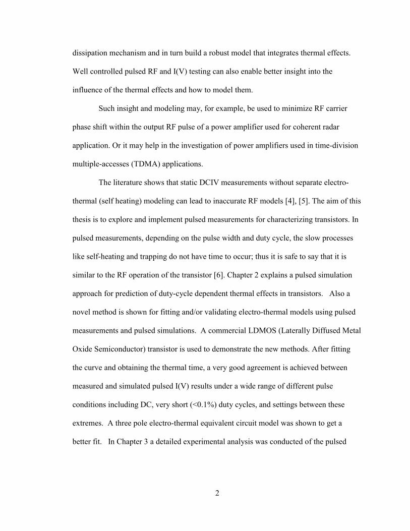
(To disable the built-in s
the MET model itself.).
Figure.2.13. Transient
Figure.2.13. sho
three pole thermal circuit
simulation and the meas
add up to the original RTH
network were adjusted to
all duty cycles considere
all values in between. W
same shape as the measu
Voltage
19
ingle pole model we set RTH and CTH to very sm
Measurement for W = 500 µs
ws the simulated to measured transient current re
t was fit and optimized until a best fit was obtai
urement. Note that the sum of the resistances w
H value of 3.2 ohms. Values for the R-C eleme
get a best fit for the simulation to match the m
d from the smallest W (0.2 µs) through the large
ith this model it can be observed that the simula
rement curve.
Time
all values within
sults after the
ned between the
as restricted to
nt values of this
easurement for
st W (1ms) and
ted curve has the
Vd (t)

20
Figure.2.14. Three-pole Electro-thermal Model (Element values shown are the Final
Optimized Values)
2.6. Measurement and Simulation Comparison
From Figure.2.16 it can be clearly seen that the MET model with multi-pole
model is now able to predict the actual pulsed I(V) measurement very accurately which is
very important in non-linear transistor design.
The electro-thermal circuit of Figure.2.14 was used along with the pre-existing
MET model (extracted by Modelithics, Inc.) for the MRF281Z device and a good
agreement was demonstrated between the simulation and the measurement for pulsed
I(V) with different pulse widths as shown in Figure 2.16.
CC9C=0.95 uF {t}
CC8C=944 uF {t}
CC7C=74 uF {t}
RR9R=1
RR8R=1.0
RR7R=1.2

21
(a)
(b)
Figure.2.15. Comparison Between Id Measured and Simulated at Vd = 14 V and Vg =
8 V (After τ Th Extraction) (a) in Linear Scale, (b) Log Scale. Measurements were
taken with an Auriga AU4750
Auriga measurement Simulated Id
Simulated Id Auriga measurement

22
Figure.2.16. Comparison Between Pulsed I(V) Simulated and Measured After τ Th
Extraction for Varied Duty Cycles for a Single Pole Model
Pulsed measurement Static measurement
1000 µs
Pulsed measurement Static measurement
200 µs
Pulsed measurement Static measurement
0.2 µs

23
The Normalized Difference Unit (NDU) method as discussed in [11] has been
used here to quantitatively compare the relative error between the simulation and
measurement for various pulse widths as shown in Table.2.2
Table.2.2. NDU for Different W
Pulse Width (µs)
NDU Before τ Th Extraction
NDU After single-poleτ Th
Extraction
NDU After
Three-poleτ Th
Extraction
0.2 µs 0.084 0.085 0.072
2 µs 0.080 0.081 0.065
5 µs 0.079 0.082 0.075
20 µs 0.088 0.091 0.073
50 µs 0.116 0.094 0.075
200 µs 0.175 0.096 0.079
500 µs 0.169 0.089 0.081
1000 µs 0.170 0.076 0.082
From Table.2.2 and Figure 2.11 it can be observed that after single-pole τ Th
extraction (by curve fitting) the model seems to predict the device performance more
accurately at smaller W but fails to predict the measurements at W > 20 µs. From Figure
2.15 it can be observed that after the three-pole circuit extraction the new model is able to
predict the device performance very accurately from static to very small W.
24
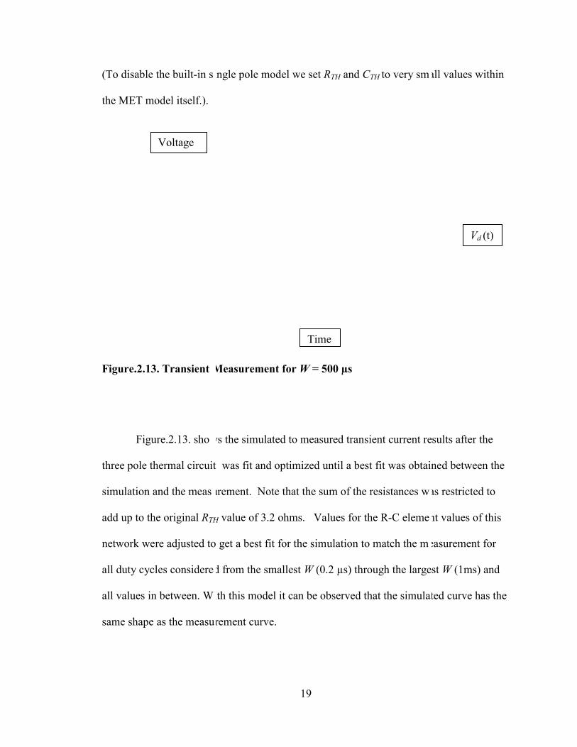
In Table 2.1 Simulation is after the model has been fit to data using Auriga’s
pulsed I(V) measurements. A graphical representation in linear scale is shown in Figure
2.17.
Figure.2.17. Comparison between Transient Measurement, Auriga_Measurement
and Modified MET Model Simulation Id for an LDMOS Transistor
So after careful modification now we have a LDMOS thermal model whose time
constant is verified by both the transient method and the Auriga’s measurements.
0
0.2
0.4
0.6
0.8
1
1.2
0.00E+00 2.00E-04 4.00E-04 6.00E-04 8.00E-04 1.00E-03
Transient measurement
Auriga_Measurement
Simulation

25
(a) Linear scale
(b) LOG scale Figure.2.18.Comparison Between the Auriga Measurement and Simulation After
Modifying the Thermal Network in Linear and Log Scale
Auriga measurement Simulated Id
Auriga measurement Simulated Id

26
2.7. Summary
In this chapter a new approach was developed for prediction of duty cycle
dependent self-heating in LDMOS transistors. A modified MET model has been shown
to fit pulsed I(V) measurements for a wide range of duty cycles. The transient current
predicted by the modified MET model also agrees very well with a conventional transient
measurement.
27
CHAPTER 3
PULSED LOAD-PULL SYSTEM SET-UP AND CONSIDERATIONS
Pulsed load-pull measurements have several advantages over CW load-pull
testing. By using pulsed load-pull we can test an amplifier under the same condition in
which it is going to be used, if in fact the final application is pulsed. An example of this
kind of application is RADAR or telecommunication base station where the amplifier is
used with pulsed or modulated signals respectively. Also pulsed operations may be more
linear than CW operation; this is due to the absence of weak thermally induced
nonlinearity under pulsed condition [3]. Pulsed operation when combined with high DC
voltage levels can also be very interesting for the validation of nonlinear models which
take into account thermal and trapping effects, and can be used to test large devices that
could not be tested at the same power levels under CW conditions due to excessive self-
heating. Pulsed signals can also be used as a first indicator of a power amplifier’s peak
capability, however complex modulated signals of the final application (IS95,
WCDMA.etc.,) should ultimately be used to find the realistic peak power capability of a
power transistor under the corresponding thermal loading as shown in Figure.3.1 [19].
New generations of transistors for power applications, in the field of mobile
communication systems (e.g. GSM phones and base stations) and radars, require accurate
non-linear models applicable for a variety of operating conditions. While non-linear, so-
called “compact”, models have become widely available for RF transistors, not all

28
models properly address self-heating effects and in particular the literature shows few
treatments that validate the time varying nature of self-heating for slowly varying signals
or sufficiently long pulses.
Figure.3.1. Plot showing the optimum load impedance location on the smith chart
for CW, IS95 and pulsed modulation formats for a 50 W Enhancement-Mode
LDMOS [19]
In particular, some popular technologies (such as VDMOS) that have recently
proven their validity in handling high power densities, suffer from thermal degradation of
performances, basically due to current collapse. In such cases, electro thermal models are
needed to properly predict this degradation. On-wafer measurements of large gate-width
power devices can be difficult in CW operation, due to the wafer insufficient heat
sinking. To overcome these problems, pulsed operation is becoming more commonly

29
used for microwave device characterization and model validation measurements [20].
Since then, pulsed I-V and pulsed S-parameter measurements have been widely used to
extract electro thermal models of different technology devices [20]-[26]. Such models
were generally verified by other (non-linear) measurement techniques, such as load-pull.
More recently, the interest in pulsed measurements has grown and the need for pulsed
non-linear measurements under different loading and bias conditions has become more
clear [27]. One other important requirement to perform pulsed and modulated signal
load-pull comes from the fact that these signals exert different thermal loading on the
device and consequently the optimum load impedance for each modulation format is also
different as shown in Figure.4.1 [19]. The importance of addressing self-heating effects
for LDMOS devices has also been pointed out [11], [16] and [28].
Before developing a pulsed load-pull set-up a brief literature review is provided of
approaches to pulsed load-pull measurements. A discussion follows of how pulsed RF
signals can be generated and how thermal and diode sensors are used for measuring
pulsed power and associated dynamic range issues. The limitations and tradeoffs
involved with non-ideal switch performance, used to pulse the input is studied to
understand that have to be made.
3.1. Background
The literature shows that there are different approaches to construct a pulsed load-
pull bench. A pulsed load-pull bench was developed using pulsed bias tees, RF source
synchronized using a pulse generator, and digitizing scope in [1] and was used to monitor
the current and a peak power meter to monitor the RF power. In this experiment the

30
pulsed power is achieved by 5µs pulse width on gate side, a 3 µs pulse width for the drain
and 2 µs pulse width for the RF signal (f=10 GHZ) [1], the duty cycle was set to 1%.
Figure.3.2 shows a comparison between CW and pulsed condition for Pout Vs Pin for the
DUT (Device Under Test which was GaN HEMT).
Figure.3.2. Pout Vs Pin with CW and Pulsed Condition [1]
Pulsed load-pull benches are also constructed using pulsed Vector Network
Analyzer (VNAs) and Large Signal Network Analyzer (LSNAs). For example, a pulsed
load-pull test bed was developed for characterizing high voltage HBTs using a pulsed
VNA to monitor the RF power profiles and sampling scope to measure the DC
current/profiles [2]. In this paper a pulse modulator connected to the output of the
microwave source is used to create the stimulus signal while four other pulsed
modulators are used to scan the pulse duration from the beginning to the end of the pulse
stimulus to see the response of the Device Under Test (AlGaN/GaN Power HEMTs), in
this case a high voltage HBT. Figure.3.3 shows the block diagram of the set-up

31
Figure.3.3. Block Diagram of the Pulsed Load-pull Set-up [2]
From the above diagram it can be observed that the stimulus modulator is used to
pulse the CW signal and the other pulse modulators are used to set the profile of the pulse
so that the response of the DUT at a specific time inside the stimulus can be observed.
Pulsed bias generator and sampling scope are used to pulse and measure the DC bias. The
pulse profiling (measurement time window) is given in Figure.3.4.

32
Figure.3.4. Pulsed RF and Bias Signal Representation [2]
Figure.3.5. (a) Pout (mW) Vs Pi (mW) and (b) PAE Vs Pin (mW) of High Voltage
HBT [2]
The authors of this work have demonstrated that using a pulsed VNA as part of a
pulsed load-pull allows control and synchronism of the repetition rate and the RF pulse
Delay_0.2 µs Delay_0.8 µs Delay_1.6 µs

33
width as well as the profile acquisition window. From Figure.3.5 it can be observed that
we have more Pout and PAE at the beginning of the pulse and decreases as the duration
within the pulse increases which clearly shows heating effect of the transistor.
3.2. Power Sensor Operation
Thermal or average sensors estimate peak pulse power using a theoretical
correction based on knowledge of the duty cycle. This is done by use of average-power
responding sensor and dividing the result by the pulse duty cycle to estimate the peak
power. This is suitable only if the modulation waveform is a rectangular pulse with a
known and constant period. Recent peak-power meter designs have started to use
advanced signal-processing to detect and analyze the actual modulation envelope of the
signal, and to use time-gated systems that measure the power only during the ON portion
of a pulse [29].
Diodes convert high-frequency energy to DC by means of their rectification
properties, which arise from their non-linear current-voltage characteristics. Figure.3.6
shows a typical diode detection curve starting near the noise level of –70 dBm and
extending up to +20 dBm. In the lower “square-law” region the diode’s detected output
voltage is linearly proportional to the input power (Vout proportional to Vin) and so
measures power directly. Above –20 dBm, the diode’s transfer characteristic transitions
toward a linear detection function and the square-law relationship is no longer valid [29].
Modern power meters perform a non-linear correction to extent the usable dynamic range
of diode sensors as discuss next.

34
Figure.3.6. Diode Detection Characteristic Range from Square Law Region
Through the Transition and Linear Region [29].
To make the diode sensor read accurate power beyond the square law region we
need an ideal sensor that would combine the accuracy and linearity of a thermal sensor
with the wide dynamic range of the corrected diode approach [29]. One other important
factor of a diode sensor is the video bandwidth, video bandwidth is the bandwidth
detectable by the sensor and meter over which the power is measured, and is sometimes
referred to as the modulation bandwidth. It is generally recommended that the power
sensor should have a rise time of no more than 1/8 of the expected signal’s raise time
[30]. For example the rise time of the pulse signal used at USF is 45 ns (from the UMTS

switch datasheet) so we
accurate pulsed power.
3.3. Pulsed Power Theo
Before taking a l
pulsed power should be r
in terms of the pulse wid
Thus the duty cy
pulse width or decreasin
is the frequency at which
The use of a ther
pulsed power Pp in terms
where fp can be calculate
important to keep in min
assumed to be rectangul
erroneous power measur
may be subject to a relati
35
need a sensor with a raise-time of < 5.6 ns in or
ry
ook at the comparison of the sensors, some basi
eviewed; for example the duty cycle of a pulse
th τ and the period T as [31]
cle of the RF pulse can be increased by either in
g the time period of the RF signal. The Pulse Re
the pulses occur and is given by
mal sensor was examined first. A thermal sens
of average power Pa as follows [32]:
Pp =
d by (2), τ is the pulse length and Pa is the avera
d that the above relationship holds good only if
ar in shape. When the pulse shape is irregular it m
ements and so a shape factor correction must be
vely large uncertainty [32].
der to measure
c terms related to
d signal is given
(3.1)
creasing the
petition Rate (fp)
(3.2)
or calculates the
(3.3)
age power. It is
the pulses can be
may lead to
applied, which

In the second set
capable of measuring pul
to predict the peak volta
and the rms power Prms i
P
where R is the resistance
To validate or qu
to be taken into account.
measurement results, mu
time period was kept con
width. When the pulsed
case of the thermal senso
The reduction in dynami
measurement with perio
Reduction
3.4. Measurement Set-u
A symbolic repre
depicted in Figure.3.7. P
port of the switch, and p
test. Figure3.8 shows th
36
of measurements, a diode sensor was used. Dio
sed power due to their fast raise time. Diode se
ge of the RF signal. The relation between the pea
s given by [33] as
Prms = =
of the load across which the diode is connected
alify a pulsed power system all the factors that i
In an attempt to isolate the effects of duty cycle
ltiple measurements of pulsed power were taken
stant and the duty cycle was changed by varyin
power is derived from an average power measu
r), the dynamic range is reduced as the duty cyc
c range from a CW measurement for a pulsed p
d T and pulse length τ can be estimated by
in Dynamic Range = 10 log
up Used to Explore Switch and Sensor Perfor
sentation of signals at different ports of the RF
ort A is the input port, port B is the signal appli
ort C is the output of the switch that is input to t
e measurement set-up, which includes a therma
de sensors are
nsors can be used
ak RF voltage
(3.4)
.
nfluence it have
e on the pulsed
n in which the
g the pulse
rement (as in the
le is lowered.
ower
(3.5)
mance
switch is
ed to the control
he device under
l sensor (Anritsu

37
MA2422B or a diode sensor (Anritsu MA2411B) an RF switch (e.g. UMCC - model #
SR-T800-2S RF switch, or a Mini-Circuits _XXYY switch), a power meter (Anritsu
ML2496A pulsed power meter or Anritsu ML2438A power meter), a signal generator
(e.g. HP 8648C), and a digital delay generator (Highland P400). The Automated Tuner
System (ATS) measurement software from Maury Microwave [34] was used to automate
the measurements and make system loss corrections as applicable. The delay generator
was used to provide the necessary logic control for the RF switch. An active-low switch
was used for the measurement: when the digital control pulse is low, the switch passes
the RF input through the switch.
Figure.3.7. RF Signal Representation at Ports A, B, and C of the RF Switch as
shown in Figure.3.8
The pulsed power calibration for a specific pulse set-up, is performed by changing
the pulse width τ of the control logic of the delay generator so that the pulse B shown in
Tτ τ

Figure.3.7 corresponds t
RF signal at to pass thro
an input insertion loss, b
such losses as a result of
pulse length is decreased
performed. The basic set
whose goal was better u
nature of the RF switch
testing. These results ar
Figure.3.8. Pulse Powe
Experimentation
38
o the desired characteristic. The RF switch TTL
ugh it. The calibration of the system showed tha
efore the DUT, of -2.451 dB. The ATS software
the calibration procedure. The reduction in dy
for a thermal sensor can be seen when a calibr
-up of Figure 3.8 was used to perform various e
nderstanding of potential limits introduced by th
as well as the power sensors for varied duty cyc
e shown in Chapter 4.
r Measurement Set-Up Used for Switch and
low allows the
t the system had
corrects for
namic range as
ation is
xperiments
e non-ideal
le swept power
Power Sensor

39
3.5. Pulsed Load-pull Theory
To understand pulsed load-pull a clear understanding of basic load-pull
measurement is essential. Load-pull in the simplest form consists of a DUT with a
calibrated tuning device on its output. The input will also be tunable but this is mainly to
boost the power gain of the device and will be changed according to each frequency to
get a good input match. Load-pull is used to measure some important parameters like
power compression, gain, inter modulation distortion (IMD) measurements, saturated
power, efficiency and linearity as the output is varied across the smith chart. Load pull
analysis is used because a network analyzer can only measure the small- signal response
of an active device but it is not possible to measure the performance under large- signal
conditions. In small-signal operation the variation around the transistor quiescent bias
point is small enough that the behavior of the signal characteristics appears linear,
whereas in large-signal model the variation about the quiescent bias point is larger and
the small-signal model is no more valid. This is where the load pull becomes important
because it can be used to gather data needed to predict the large-signal performance of
the active device.
Analyze of the load pull data is done by using a Smith chart and plotting contours
of constant output power, gain, and efficiency as shown in Figure.3.9 One observation
that can be made by looking at this figure is that unlike noise circles the power contours
are often not circular unlike noise circles no matter how carefully the system is
calibrated.
The explanation for the shape of the load-pull power contours has been given in
[35]. The first step in any load pull system is accurate S-parameter measurement of all the

40
blocks in the system. To obtain this the VNA should be calibrated very carefully. Doing
this will remove the effect of tuners, cables, connectors, attenuators, probes, and all other
components in the system and shift the reference plane for measurement to the probe tip
or the DUT. Once the VNA is calibrated and S-parameters of the individual blocks are
measured, utmost care should be taken that the set up is not disturbed. Figure.3.10 shows
the different blocks involved in a load pull set-up.
For this work a Maury Microwave Load-Pull test system was utilized along with
the Maury “ATS” Software, which is used for system calibration and measurement.
Calibration includes careful VNA measurements of all of the system components in the
RF path between the signal generator and the power sensor and/or spectrum analyzer
used to perform power or spectral measurements for varied source and load impedances.
Figure.3.9. Typical Load-pull Data [35]
-2dB-1dB
Popt

41
Figure.3.10. A Representative Load Pull Set Up [34]
After calibrating and saving the S-parameter files for all components they are
entered into the ATS Maury Software and the software controls the instruments and
tuners. Figure.3.11 shows the various blocks for which the S-parameter has to be
measured and stored. Tuner characterization consists of performing VNA testing of the
source and load tuner blocks for many different impedance settings of the tuners for each
frequency the load-pull testing is to be performed.
Figure3.11. Different Blocks Involved in a Typical Power/Intermod Measurement
[34]

42
3.6. Calibration Checks
Before measurement the characterized tuners data is entered into memory for both
the tuners. This includes the measured 2- port complete S-parameter data and the
corresponding tuner position for a number of discrete tuner positions. The tuner is
considered as the heart of the load pull set-up so it has to be characterized properly to get
accurate measurements. Before characterizing the tuner, the VNA should be calibrated
using proper high reliability cables and connectors. Set the start, stop and step size for the
frequency and then in cal type select Full 12 – term. Enter the values for the terms from
the calibration data sheet available. To check the VNA calibration performed connect the
thru and capture the data and plot S12 and S21 +/- 0.1 dB and the reflection coefficients
|S11| and |S22| should be < -40 dB. Then connect open on both ports and |S11| and |S22|
should be < + or – 0.05 db, then connect short and |S11| and |S22| should be again < + or
- 0.05 dB. Similarly after the tuner is characterized perform the same set of tests that was
explained in the previous steps to ensure your calibration.
Extra care should be taken after calibrating the VNA so that the cables do not
bend and minimum movement should be allowed. Now connect the tuner to the VNA.
The tuner’s position will be changed automatically by the tuner controller and the S-
parameter for different tuner positions will be saved in the system. After doing all the
calibrations and obtaining the tuner datas, the set-up can be verified using this procedure:
based upon the small-signal S-parameters that were entered for each block the software
will calculate a transducer gain Gt(s). The software measures the actual transducer gain
Gt which is the delivered output power to the available input power at the DUT reference
plane. ∆Gt is the difference between Gt and Gt(s); it should be less than 1or 2 db. After

43
these steps, power or intermodulation calibration has to be done before taking the actual
measurements. In pulsed load pull, the input RF single tone is pulse modulated by a
pulsed RF source or an RF switch whose pulse width can be altered as desired.
3.7. Pulsed Load-pull Set-Up:
The pulsed load-pull system used in this work is shown in Figure 3.12 with
changing duty cycle from CW to short pulse. The system uses an HP signal generator
followed by an RF switch driven with a pulsed source, an Anritsu thermal sensor and
power meter in combination with a Maury Microwave load pull system. The whole
system was controlled using Maury Automated Tuner System (ATS) software. The
advantages of pulsed load-pull and CW load-pull were clearly seen in the results of the
experiment. It was observed that pulsed load-pull allowed the device to be safely driven
to higher pulsed powers as the duty cycle was decreased.
In this set-up the UMCC - model # SR-T800-2S RF switch (1-18 GHz) was used
to pulse the input before the preamp, the power meter used was an Anritsus ML2438A
along with Anritsu thermal sensor MA2422B. A 10 W enhancement-mode vertical
MOSFET was used for this experiment.

44
Figure.3.12. Pulsed Load-pull Set-up
There were some problems with this set-up
1) When the input RF signal was pulsed with time period 2ms and pulse width
200µs (Duty Cycle = 10%) the dynamic range issue and noise floor began to
increase for the thermal sensor.
2) The formula used by Maury to calculate efficiency is given by
Efficiency = )**
(*100IinVinIoutVout
PinPout+
− (3.6)
The problem with this is when the input RF signal is pulsed the drain current Id
from the device is also in a pulse shape and since the DC signal is not pulsed a
manual correction may be needed to obtain the desired value of efficiency which
is explained later.
Input
Pre Amp
RF Switch
6 dB Broadband Attenuator

45
3) Another issue is when the duty cycle is decreased by reducing the pulse width or
increasing the time period the dynamic range of the thermal sensor starts to
reduce as the noise floor creeps up. So for small duty cycle it is advisable to use
the pulsed diode sensor.
3.8. Summary
In this chapter we reviewed various set-ups that have been used by others for
pulsed load-pull testing. A custom test bench used in this research was then described.
This bench was used with some variations for both benchmark testing of switches and
power sensors as well as the pulsed load-pull experiments described in the next chapter.
The differences between use of pulsed and thermal power sensors and related dynamic
range trade-offs were explored experimentally.

46
CHAPTER 4
PULSED LOAD-PULL SYSTEM EXPERIMENTATION AND MEASURED
RESULTS FOR SELECTED RF POWER TRANSISTORS
In this chapter results are presented first for various system experiments conducted to
better understand limitations of various components like the input RF switch, the power
sensor [36] and the bias tee (See Appendix A). Following this, pulsed load-pull results
are shown for two example high power RF power transistors: one a VDMOS device and
the other an LDMOS device.
4.1. Results of Switch and Power Sensor Experimentation
In Figure.4.1 power testing results are shown for the case of a thermal sensor and
a switch manufactured by UMCC SR-T800-2S. Figure.4.1 shows the measured pulsed
available power (at the sensor) versus the programmed power for various pulse lengths
and a constant period of 100 µs and RF signal frequency 2GHz. As we will point out,
the best approach to calibration and use of a thermal sensor is to calibrate under CW
conditions, then use the pulsed input stimulus for the DUT testing only (not calibration).
The Y axis (Pavailable) is the pulsed power calculated by Maury automatically when fp and
τ are known. It is important to note while observing this data that the thermal sensor
measures average power. For reduced pulse length (and hence reduced duty cycle) a
reduction in the dynamic range of the sensor was observed due to the fact that the power

47
is applied for a shorter amount of time, thus decreasing the average power delivered to
the sensor. The thermal sensor used has a manufacturer specified dynamic range of -
30dBm to 20dBm. Figure.4.1 shows that as expected the sensor actually has an absolute
low end that is lower than its specification (to provide some margin). For a 50 % duty
cycle (in the Figure.4.1 case a 50 µs pulse length), the average power detected by the
sensor at each pulsed power setting is approximately 3 dBm lower than in the continuous-
power case. For the 50 % case, it would be expected that a pulsed power of -30+3 = -27
dBm would be the lowest pulsed power recommended to be measurable by the sensor,
based on the specified range.
For a duty cycle of 5 percent (5 µs pulse length) the average power that can be
measured in each setting is reduced by approximately 13 dB, this effect can be clearly
observed from Figure.4.1. In Figure.4.2 the same plot with Y axis as average Pout
(available) is shown. Here it can be clearly observed that the lower limit of the sensor is
actually around -39 dBm where it hits the noise floor. Because the specification for the
low-power measurement limit of the sensor is -30 dBm (the actual observed lower limit
during the experiments was -34 dBm), for the case of a 5 percent duty cycle, the lower
limit for pulse power is (-30 + 13) = -17 dBm. This is consistent with the results in
Figure3.4. (a). The results in Figure.4.1 (b) indicate that this setting allows measurements
to about -20 or -21 dBm (the sensor seems to show a trend of possessing a “noise floor”
about 3 or 4 dB lower than would be calculated from the specification).
Due to the noise and reduction in dynamic range as the duty cycle is reduced,
deterioration in the precision of the measurements can be observed. From Figure.4.1 it
can be seen that the low pulsed-power measurement limit of the sensor is relatively high

48
for very low pulse lengths. In Figure.4.2 it can be seen that for 0.5 µs the sensor response
is in the noise floor until a Pin of -11 dBm. At 0.1 µs the lowest power (Pavailable) that
could be accurately measured is -4 dBm. This low duty cycle deterioration is present for
both calibration as well as DUT testing.
Further experimentation was performed using calibration under both pulsed and
CW conditions, and these tests showed that the best approach is to calibrate under CW
conditions prior to performing DUT testing under the desired duty cycle. The reasoning
for this is sound: the sensor measures average power, so calibrating with larger average
power values will enhance the precision of both the calibration and the ensuing
measurements.
Figure 4.3 shows the calibration results using a diode sensor (for comparison with
Figure.4.1). It can be observed that the diode sensor exhibits no low-power dynamic
range issue for pulses tested between 90 and 0.5 µs. For pulse lengths below 0.5 µs,
some problems are observed with the diode sensor measurements.

49
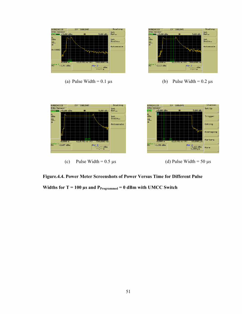
Figure.4.1. Calibration Data: Pinprogrammed Versus pulsed Poutavailable for Thermal
Sensor for Various RF Pulse Width and Constant Period of 100 µs
Figure.4.2. Calibration Data: Pinprogrammed Versus Average Poutavailable for Thermal
Sensor for Various RF Pulse Width and Constant Period of 100 µs
-40
-30
-20
-10
0
10
20
-40 -30 -20 -10 0 10 20
CW
90 us
70 us
50 us
20 us
5 us
1 us
0.5 us
0.1 us
Pout (available)dBm
Pin (programmed) dBm

Figure.4.3. Calibration
Various RF Pulse Widt
Since a diode sen
power as shown in equat
set-up and found that the
power versus time as vie
input power of 0 dBm. T
measured between the t
the power-versus-time vi
Pin (programmed) dB
50
Data: Pavailable Versus Pprogrammed for Diode S
h and Constant Period of 100 µs with UMCC
sor uses gate to measure the peak voltage and c
ion 3.4 it is more accurate, so we did a thoroug
switch was limiting the smaller pulse widths. F
wed by the power meter for several different pu
he power meter has been configured to report t
wo vertical cursors shown on the screen view.
ew for a significantly lower input power value (
Pout (available)dBm
m
ensor for
Switch
alculates pulsed
h analysis of the
igure.4.4. shows
lse lengths at an
he average power
Figure.4.5 shows
-20 dBm).
51
(a) Pulse Width = 0.1 µs
(b) Pulse Width = 0.2 µs
(c) Pulse Width = 0.5 µs
(d) Pulse Width = 50 µs
Figure.4.4. Power Meter Screenshots of Power Versus Time for Different Pulse
Widths for T = 100 µs and PProgrammed = 0 dBm with UMCC Switch

52
(a) Pulse Width = 0.1 µs
Figure.4.5. Power Meter Screenshots of Power Versus Time for Different Pulse
Widths for T = 100 µs and Pprogrammed = -20 dBm with UMCC Switch
In this case, it appears that, while a satisfactorily flat region can still be used to
obtain a reasonable measurement at the 0.5 µs pulse length, the power trace in the 0.2 and
0.1 µs cases appears very uneven, and it is difficult to place the cursors to get an accurate
measurement. This seems to be a reasonable explanation for the difficulty in obtaining
accurate low-power calibrations for the 0.1 and 0.2 µs pulse lengths in Figure.4.3. It was
concluded that caution should be exercised when attempting to measure using this set-up
for 0.1 µs and 0.2 µs pulse lengths for low power values.
The use of a different RF switch (Minicircuit ZFSWA-2-46) has been shown to
produce more favorable results for these lower duty cycles as shown in Figure.4.6 and
Figure.4.7.
(b) Pulse Width = 0.2 µs

53
(a) Pulse Width = 0.1 µs
(b) Pulse Width = 0.2 µs
(c) Pulse Width = 0.5 µs
(d) Pulse Width = 50 µs
Figure.4.6. Power Meter Screenshots of Power Versus Time for Different Pulse
Widths for T = 100 µs and PProgrammed = 0 dBm with Minicircuits Switch

54
(a) Pulse Width = 0.1 µs
(b) Pulse Width = 0.2 µs
Figure.4.7. Power Meter Screenshots of Power Versus Time for Different Pulse
Widths for T = 100 µs and Pprogrammed = -20 dBm with Minicircuits Switch
Figure.4.8. Calibration Data: Pavailable Versus Pprogrammed for Diode Sensor for
Various RF Pulse Width and Constant Period of 100 µs with Minicircuits Switch
-30
-25
-20
-15
-10
-5
0
5
10
15
-25 -20 -15 -10 -5 0 5 10 15 20
0.1 us
0.5 us
1 us
5 us
20 us
50 us
70 us
90 us
CW

55
From Figure.4.8 it concluded that the Minicircuit Switch has a much better
response for lower pulse widths. Figure.4.9 shows a comparison between the measured
Gt of the thru for both of the sensors at a pulse length τ = 0.5 µs pulse length during a
power sweep. For these results the set-up with the UMC switch was used. Ideally Gt
should be zero for all power levels, but it can be observed that the thermal sensor loses
precision at lower input power values. Also note that the diode sensor used in this set-up
had a stated dynamic range of - 20 to +20 dBm, compared to -30 dBm to +20 dBm for
the thermal sensor. However, in our application the thermal sensor is being used to
measure average power over a large time span including both on and off pulse conditions,
whereas the diode sensor is used to measure the signal during a gated interval during the
on time of the pulse, where more significant power levels are maintained. Accordingly,
the diode sensor has a clear advantage for lower pulse ranges because the signal can be
gated and it can be decided under which time period the power should be measured.
From Figure.4.9 it can be clearly observed that precision begins to deteriorate
significantly for the thermal sensor as the pulsed power goes below about -5 dBm.
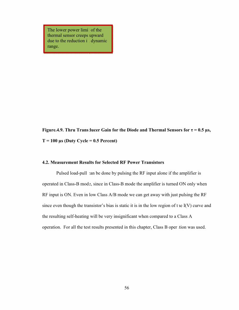
Figure.4.9. Thru Trans
T = 100 µs (Duty Cycle
4.2. Measurement Resu
Pulsed load-pull
operated in Class-B mod
RF input is ON. Even in
since even though the tra
the resulting self-heating
operation. For all the tes
The lower power limithermal sensor creeps due to the reduction irange.
56
ducer Gain for the Diode and Thermal Senso
= 0.5 Percent)
lts for Selected RF Power Transistors
can be done by pulsing the RF input alone if the
e, since in Class-B mode the amplifier is turned
low Class A/B mode we can get away with just
nsistor’s bias is static it is in the low region of t
will be very insignificant when compared to a C
t results presented in this chapter, Class B oper
t of the upward
n dynamic
rs for τ = 0.5 µs,
amplifier is
ON only when
pulsing the RF
he I(V) curve and
Class A
ation was used.

57
4.3. Measurements on a Selected VDMOS Transistor
For doing pulsed measurements Maury has an option (as shown in Figure.4.10)
where the user can enter the duty cycle of the waveform and this way Maury will
automatically calculate the pulsed power. Pulsed load-pull was performed on a selected
high power vertical MOS device using a time period 2ms and pulse width 200µs (Duty
Cycle = 10%). After characterizing the system and tuners, a power calibration is done
with a thru connection in place of the DUT.
Figure.4.10. Pulsed Power Options in Maury v3

After calibrating
shown below. There are
find the best way to do it
1) Swept power cali
power sweep in t
2) Swept power cal
power sweep in p
3) Swept power cali
power sweep
[Note: in all the p
pulse width was
Figure.4.11. sho
Figure4.11. Gain Gt of
Gt
58
the system for power, the DUT was measured a
two different ways to make a pulsed power mea
three type of power sweeps were made with the
bration with a CW input signal and then measur
he same CW mode
ibration with a CW input signal and then measu
ulsed condition
bration with a pulsed signal and then do the 50
ulsed condition shown below the time period w
200µs (Duty Cycle = 10%)]
ws the variation in the Gt of the device
the Device at Various Conditions
Pin
Puls
nd the results are
surement so to
e DUT:
e the 50 Ohm
re the 50 Ohm
Ohm pulsed
as kept 2ms and
ed more gain

From this plot it
form the device as explai
lower input powers this i
Figure.4.5 the pulse is n
the thermal sensor. The
Figure.4.12. Pin Vs Pou
Even here it can
under large-signal drive.
these conditions. But, as
software a correction has
4.4. Efficiency Correcti
The formula for efficien
E
Pout
59
can be clearly seen that the pulsed signal gets m
ned earlier. Also the red and blue curves are no
s because at lower pulse width/input power as s
ot perfectly rectangular in shape and this causes
next figure shows the Pin vs Pout for the DUT
t for the DUT at Various Measurement Con
be observed that the pulsed condition has more
Figure.4.13 shows the efficiency measurement o
explained above when calculating efficiency us
to be applied.
on
cy as give in equation 3.6 is
fficiency = )**
(*100IinVinIoutVout
PinPout+
−
Pin
ore output power
t together at
hown before in
inaccuracies in
ditions
output power
of the DUT at
ing Maury
In the above the i
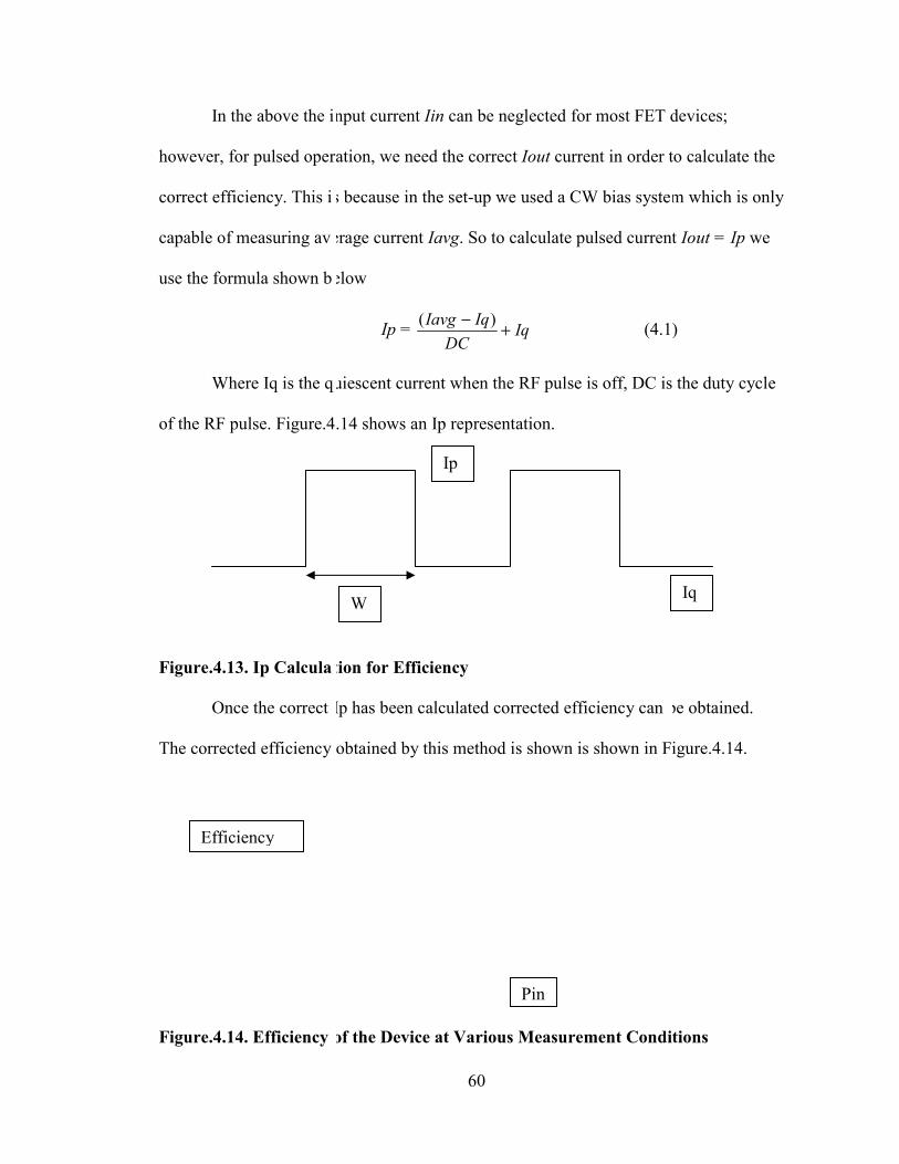
however, for pulsed oper
correct efficiency. This i
capable of measuring av
use the formula shown b
Where Iq is the q
of the RF pulse. Figure.4
Figure.4.13. Ip Calcula
Once the correct
The corrected efficiency
Figure.4.14. Efficiency
Efficiency
60
nput current Iin can be neglected for most FET d
ation, we need the correct Iout current in order t
s because in the set-up we used a CW bias syste
erage current Iavg. So to calculate pulsed curren
elow
Ip = IqDC
IqIavg +− )( (4.1
uiescent current when the RF pulse is off, DC is
.14 shows an Ip representation.
tion for Efficiency
Ip has been calculated corrected efficiency can
obtained by this method is shown is shown in F
of the Device at Various Measurement Condi
Pin
Ip
W
devices;
to calculate the
m which is only
t Iout = Ip we
)
the duty cycle
be obtained.
igure.4.14.
tions
Iq

61
From all the three measurements shown above it can be seen that the pulsed
power sweep with the CW calibration is the most favorable one. This is because when a
pulsed calibration is done at 10% duty cycle using a thermal sensor the noise floor
increases and the range of the sensor is reduced, and when a pulsed measurement is done
with the same calibration the errors in the lower range gets carried over to the
measurement but when a CW calibration is done the entire range of the sensor is
calibrated; then when we do a pulsed measurement we have the entire range of the sensor
even thought the lower power ranges might have some error. This explanation is clearly
seen from the graphs shown above.
Table.4.1. Pulsed and CW load-pull comparison for different frequencies
Load-pull Condition
Frequency Ghz
Pin dBm Opt Load Pout dBm
Gain dB
CW 0.9 13 0.6416 < 149.27
32.24 19.24
Pulsed 0.6055 < 155.61
32.69 19.69
CW 1.2 17 0.7441 < -175.21
32.4 15.4
Pulsed 0.6506 < -177.18
33.26 16.26
CW 2.1 14 0.8032 < -80.06
29.46 15.46
Pulsed 0.7914 < -79.91
29.93 15.93

62
Following characterization and determination of the calibration type, the actual
pulsed load-pull was done for the DUT. The pulsed load-pull measurements were done at
three different frequencies 0.9GHz, 1.2 GHz and 2.1 GHz. Figure.4.15 and Figure.4.16
shows the CW and Pulsed load-pull performed respectively from these figures it can be
seen that the pulsed load-pull has more gain and Pout. The Table.4.1 below shows the
gain and Pout 1 dBm for the various frequencies. Even though the difference may not
always be significant, the pulsed operation is safer for the device which will be explained
in the later part.
From Figure.4.15 and Figure.4.16 it can be seen that the pulse and CW
load-pull measurements have different optimum load impedance, as discussed in [19].
Also, pulsed load-pull has more gain and Pout when compared to CW measurement.
Some experiments were done with the pulsed load-pull system where the time period was
kept constant at 2 ms and the pulse width was varied between 200 µs and 400 µs for the
variation of duty cycle from 10% to 20%. Figure.4.17 show that, as the duty cycle (pulse
width) increases the device is pushed into more compression earlier.

63
Figure.4.15. CW Load-pull

64
Figure.4.16. Pulsed Load-pull with DC 10%

65
Figure.4.17. Power Sweep with Opt Load Г for Max Power and Opt Source Г for
Gain
In Figure.4.18 it can be observed that the gain of the DUT has decreased and pushed into
compression sooner. Figure.4.19 shows the efficiency plot (with corrected Iout for pulsed
current) of the DUT for the same conditions and it can be seen that the efficiency is found
compress at a higher rate for 20% when compared to 80% duty cycle due the self-heating
and decrease in Pout.
These results show the importance of pulsed load-pull in testing the device in
linear safe region.

66
Figure.4.18. Gain Comparison for Different Pulse Width/ Duty Cycle
Figure.4.19. Efficiency Comparison for Different Pulsed Widths / Duty Cycles
0
5
10
15
20
25
30
0 5 10 1 25 30
10 % DC
20 % DC
Pin
Efficiency

4.5. Pulsed Load Pull fo
In this section pulsed
amplifier. The device wa
input is ON.
4.6. Measurement Resu
Figure.4.20 show
and S = 100 µs) to CW. I
device is affected by self
Figure.4.20. Pin Vs Pou
V and Vds = 7.5 V
The device was p
noted as the RF power is
Pout
67
or a Selected LDMOS Transistor
load-pull is performed on a LDMOS 10 W tran
s operated in class B condition so that it turns O
lts:
s the Pin Vs Pout for various duty cycles form 1
t can be clearly seen from the figures shown bel
heating.
t for the LDMOS Transistor Under Various
ushed till 3 dB compression. But from Figure.4.
increased the device experiences more heating.
Pin
smission
ON when the RF
0 µs (W = 10 µs
low that the
W with Vgs = 1.8
20 it can be
Figure.4.21

shows the Pin Vs Gain c
W is not suffering from a
gain. From Figure.4.22 t
W can be clearly seen.
Figure.4.21. Pin Vs Gain
V and Vds = 7.5 V
Gt
68
urves for different W, even here it can be observ
ny self heating but as the W increase we can se
he difference in Efficiency (with corrected Iout)
n for the LDMOS Transistor Under Various
Pin
ed that the 10 µs
e the decrease in
for the various
W with Vgs = 1.8

69
Figure.4.22. Pin Vs Efficiency for the LDMOS Transistor Under Various W with Vgs
= 1.8 V and Vds = 7.5 V
Also in the above figure it is evident that thought the efficiency is higher as we
increase the W the efficiency compresses at a higher rate for larger Ws. It can be noted
that for all the Ws > 10 µs reach the 3 dB compression sooner than the 10 µs W.
0
5
10
15
20
25
30
40
45
50
12 17 22 27 32 37
10 us
40us
60 us
80 us
CW
Efficiency
Pin

70
The next figure shows the pulsed load-pull set-up used with the Minicircuits switch
Figure.4.23. Pulsed Load-pull Set-up used for LDMOS Measurement with Labels
Indicating the Different Points where the Oscilloscope Measurement was made.
D C
Input
Isolator
A
Digital Delay Generator
Pre Amp
RF Switch
B

(a)
(c)
Figure.4.24. Oscillosco
System for a W of 50 µs
From Figure.4.24
signal generator but as it
added. The last figure in
the device.
71
(b)
(d)
pe Measurement at Different Points in the Pu
it can be noted that the pulsed signal is clean at
passes through the switch and pre-amplifier mo
Figure.4.24 (d) shows the pulsed signal after a
lsed Load-pull
the digital
re noise is
mplification from

72
4.7. Summary
In this chapter a simple benchmarking technique was explained to explore
potential system limitations. Also the tradeoffs involved in choosing a thermal sensor
over a diode sensor were shown. After gaining confidence with the power bench pulsed
load-pull was done on VDMOS and LDMOS transistors. From the results shown it is
evident that pulsed load-pull has more Pout and gain and less compression when
compared to CW condition. Also since both the devices where operated in Class B
condition the significant difference in Pout, Gain and Efficiency appear at high Pin where
the bias of the device is also higher.

73
CHAPTER 5
CONCLUSIONS AND RECOMMENDATIONS
This thesis has explored pulsed I (V) simulation technique to predict duty-cycle
dependent self-heating has been demonstrated using a MET model for a power MOSFET.
This simulation technique provides an additional reliable (and likely more convenient)
method to extract the thermal time constant τ Th by doing a curve fitting between the
pulsed I(V) simulation of an electro-thermal non-linear model and the pulsed I(V)
measured data with varied duty cycles. By using this simulation method, an custom
transient measurement set-up to extract the thermal time constant can be avoided.
Parameters for a three pole electro-thermal circuit was obtained and shown to have a
better fit than a simple single-pole electro-thermal circuit for the MOSFET used in the
experiments.
A secondary goal of the thesis was to explore pulsed load-pull measurements. As
part of this, a thorough analysis of the pulsed power system was done. The results of an
experiment to compare the accuracy and precision of pulsed power measurements using
two different types of power sensors were shown. Pulsed power measurements for
various duty cycles have been analyzed. As expected, the dynamic range of the thermal
sensor used reduces as the duty cycle reduces, while the diode sensor set-up produced
more accurate readings for lower duty cycle values. Limitations of the diode sensor to
measure for low duty cycles at low power values were traced to limitations of the pulse

74
shape generated by the RF switch used. The benchmark methods outlined here shold
prove helpful in developing confidence in a given test system, and provide insight on
what duty cycles and power ranges can be used with confidence for testing of active
devices.
In the final chapter pulsed load-pull results are presented. Testing was performed
on example VDMOS and LDMOS transistors. Both these devices were operated in Class
B operation (Vg < Vth). In this case, the device turns ON when the RF input in ON, i.e.,
the device bias is controlled by the RF signal. This is evident as in all Pin Vs Pout and
Pin Vs Gain curves the increase in heating (decrease in Pout or Gain) is always at the
high RF power region, which of course correspond to the highest current and highest
thermal power dissipation. Careful attention to correcting the obtained efficiency data by
estimating the peak current was important to obtaining efficiency data.
This work has given rise to several areas where further study. Following the
modification in the MET model for self-heating more work can be done to show how to
apply similar pulsed I(V) simulation techniques to address devices with trapping (eg.,
GaAS pHEMTs and GaN HEMTs). Pulsed load-pull developed by this work can be
further advanced to measure devices in high class AB or class A bias condition by using a
pulsed bias system which is synchronized with the pulsed RF source. Further pulsed load-
pull simulation can be performed in ADS by using envelop simulation for suitable
models.

75
REFERENCES
[1] S. Nuttinck, E. Gebara, J. Laskar, and M. Harris, “Study of Self-Heating Effects, Temperature-Dependent Modeling, and Pulsed Load-pull Measurements on GaN HEMTs”, IEEE MTT-S 2001, Phoenix, Proceedings, Vol.3, pp.2151-2123. [2] H. Bousbia, D. Barataud, G. Neveux, T. Gasseling, J.M. Nebus and J.P. Teyssier, “A Novel Load-Pull Setup Allowing the Intermodulation Measurement of Power Transistors under Pulsed DC and Pulsed RF Conditions”, Microwave Theory and Techniques Society Digest, June 2006, pp. 1452-1455. [3] V. Teppati, A. Ferrero, V. Niculae, and U. Pisani, “A Novel Pulsed Load-Pull and S-Parameter Integrated Measurement System”, Intrumentation and Measurement Technology Conference, Como, Italy, May 2004. [4] P. Ladbrooke and J. Bridge, “The Importance of the Current-Voltage Characteristics of FETs, HEMTs, and Bipolar Transistors in Contemporary Circuit Design,” Microwave Journal, March 2002. [5] A. Platzker, A. Palevsky, S. Nash, W. Struble, Y. Tajima, “Characterization of GaAs Devices by a Versatile Pulsed I-V Measurement System,” IEEE Microwave Theory and Techniques Society Digest, 1990. [6] L. Dunleavy, W. Clausen, and T. Weller, “Pulsed IV for Nonlinear Modeling,” Microwave Journal, March 2003. [7] C. Baylis II, Master’s Thesis: “Improved Current-Voltage Methods for RF Transistor Characterization”, Tampa, Florida: University of South Florida, 2004. [8] P. Winson, Characterization and Modeling of GaAs Schottky Barrier Diodes Using an Integrated Pulsed I-V / Pulsed S-Parameter Test Set, Master’s Thesis, University of South Florida, 1992. [9] W.R. Curtice, J.A. Pla, D. Bridges, T. Liang and E.E. Shumate, “A New Dynamic Electro-Thermal Nonlinear Model for Silicon RF LDMOS FET’s,” IEEE MTT-S International Microwave Symposium, Anaheim, CA, pp.419-422.

76
[10] S.M. Somasundaram, C. Baylis, L. Dunleavy, M. Marbell, “Duty Cycle Depended Pulsed IV Simulation and Thermal Time Constant Model Fitting for LDMOS Transistors,” 74th Automatic RF Techniques Group (ARFTG) Conference, Broomfield/Boulder, CO, December 2009 [11] C. Baylis II, Lawrence P. Dunleavy, John E. Daniel, “Direct Measurement of Thermal Circuit Parameters Using Pulsed IV and the Normalized Difference Unit,” IEEE MTT-S Int’l Microwave Symposium, 2004. [12] L. Lucas and B. Ricco, “Modeling Temperature Effects in the DC I-V Characteristics of GaAs MESFETS’s,” IEEE Transaction on Electron Devices,Vol. 40, No. 2, February 1993, pp. 273-277. [13] J.P. Teyssier, J.P. Viaud, J.J. Raoux , and R. Quere, “Fully Integrated Nonlinear Modeling and Characterization System of Microwave Transistors with On-Wafer Pulsed Measurements,” IEEE Microwave Symposium Digest, Vol. 3, May 1995, pp. 1033-1036. [14] J.F. Vidalou, L.F. Grossier, M. Chaumas, M. Camiade, P. Roux and J. Obregon, “Accurate Nonlinear Transistor Modeling Using Pulsed S Parameters Measurements Under Pulsed Bias Condition,” IEEE Microwave Symposium Digest, Vol. 1, June 1991, pp. 95-98. [15] T. Fernandez, Y. Newport, J.M. Zamanillo, A. Tazon and A. Mediavilla, “Extracting a Bias-Dependent Large Signal MESFET Model from Pulsed I/V Measuremetns,” IEEE MTT Transactions, Vol.44, No.3, March 1996, pp. 372-378. [16] C. Baylis, and L. Dunleavy, “Voltage Transient Measurement and Extraction of Power RF MOSFET Thermal Time Constants,” 70th Automatic RF Techniques Group (ARFTG) Conference, Arizona, November 2007. [17] Y. Yang, Y. Woo, J. Yi, and B. Kim, “A New Empirical Large-Signal Model of Si LDMOSFETs for High-Power Amplifier Design,” IEEE Transactions on Microwave Theory and Techniques. Vol.49, Issue 9, September 2001, pp. 1626-1633. [18] C. Anghel, R. Gillon, and A.M. Ionescu, “Self-Heating Characterization and Extraction Method for Thermal Resistance and Capacitance in HV MOSFETs”, IEEE Electron Device Letters, Vol. 25, No. 3, March 2004, pp. 141-143. [19] B.Noori, P.Aaen, D.Abdo, P.Hart; “RF Power Behind Design Innovation”, Microwave Design Whitepaper, May 2007. [20] J.M. Collantes, J.J. Raoux, J.P. Villotte, R. Quere, G. Montoriol and F. Dupis, “A New Large Signal model Based on Pulsed Measurement Techniques for RF Power Mosfet,” in Microwave Symposium Digest 1995, vol.3, Orlando, FL, May 1995, pp, 1553-1556.

77
[21] A. Mallet, D. Floriot, J.P. Viaud, F. Blache, J.M. Nebus, and S. Delage, “A 90% Power-Added Efficiency gamp/gaas HBT for I-Band Radar and Mobile Communication Sytem,” IEEE Microwave and Guided Wave Letters, vol.6, pp 132-134, Mar.1996. [22] A. Mallet, T. Peyretailade, R. Sommet, D. Florit, S. Delage, J.M. Nebus, and J. Obregon, “ A Design Method for High Efficiency Class F HBT Amplifiers,” in Microwave Symposium Digest 1996, vol.2, San Francisco, CA, June 1996, pp 855-858. [23] T. Peyretaillade, M. Perez, S. Mons, R. Sommet, Ph. Auzemery, J.C. Lalaurie, and R. Quere, “ A Pulsed Measurement Based Electrothermal Model of HBT with Thermal Stability Prediction Capabilities,” in Microwave Symposium Digest, 1997, vol.3, Denver, CO, June 1997, pp 1515-1518. [24] J.M. Collantes, P. Bouysse, and R. Quere, “Characteristics and Modelling Thermal Behaviour of Radio-Frequency Power LDMOS Transistors,” Electronic Letters, vol. 34, pp. 1428-1430, July 1998 [25] D. Siriex, O. Noblane, D. Baratand, E. Chartier, C. Brylinski, and R. Quere, “A EAD-Oriented nonlinear Model of SiE MESFET Based on Pulsed I(V) Pulsed S-parameter Measurements,” IEEE Transactions on Electron Devices, vol.46, pp. 580-584, mar. 1999. [26] K. Koh, H.M. Park, and S. Hong, “A Large-Signal FET Model Including Thermal and Trap Effects with Pulsed I-V Measurements,” in Microwave Symposium Digest, 2003, vol.1, Philadelphia, PA, June 2003, pp. 467-470. [27] J. Mohan, P. Ersland, C. Weichert, M. Lally, J.P. Lanteri, “On-Wafer Pulsed Power Vector Testing”, in Proc, ARFTG Conf., Dallas, TE, May 1990, p82. [28] W. Curtice, L. Dunleavy, W. Clausen and R. Pengelly, “New LDMOS Model Delivers Powerful Transistor Library – Part I: The CMC Model”, High Frequency Electronics, October 2004. [29] Y.Brian Lee, “Functional Tests for Peak Power Sensor and Meter”, ARFTG 2004, pg 197-205. [30] Agilent product note “Choosing the right Power meter and Sensor”. [31] Agilent application note 1449-2 “Fundamentals of RF and Microwave Power Measurement (Part 2)” [32] C. Baylis, L. Dunleavy, and J. Martens, “Construction and Benchmarking of a Pulsed S-Parameter Measurement System”, Automatic RF Techniques Group (ARFTG) Conference, Washington, DC, December 2005

78
[33] PA. Hudson, “Measurement of RF Peak Pulse Power”, Proceedings of IEEE, Vol. 55, No. 6, June 1967, pp. 851-855. [34] Maury Microwave, 2900 Inland Empire Blvd, Ontario, California 91764 USA, [http://www.maurymw.com/index.htm] [35] S.C. Cripps, “RF Power Amplifiers for Wireless Communication” [36] S.M. Somasundaram, C. Baylis, L. Dunleavy, “Benchmarking Comparison of Thermal and Diode Sensors for Pulsed Power Measurement,” 72nd Automatic RF Techniques Group (ARFTG) Conference, Portland, OR, December 2008

79
APPENDICES

80
Appendix A: Pulsed Bias Tee Measurements
In Chapter 4 the pulsed load-pull bench was discussed. In that chapter we saw how different components in the bench can cause errors in the pulsed power measurements. Bias tee form an important components of the pulsed power system i.e., the bias tee’s DC path should allows bias pulses to pass through to the device unchanged, while still allowing RF measurements at as low a frequency as possible.
All the bias tees were tested under two pulsed conditions
(1) Pulse width 8 us and period 80 us (10% duty cycle)
(2) Pulse width 4 us and period 80 us (5% duty cycle). Digital Delay Generator was used to generate the pulses.
Figure.A.1 show the set-up used
Figure.A.1. Bias Tee Measurement Set-up
The digital delay generator’s pulse was used to give the pulsed signal needed to check the DC path of the bias tees. The results are shown below.
Input pulsed signals from Digital Delay Generator
Oscilloscope for checking the integrity of the pulsed output signal

81
Appendix A (Continued)
Results:
Totally four bias tees were tested for the project
1) Picoseconds lab bias tee 5587
Figure.A.2. Pulse Width 8 µs and Period 80 µs (10% Duty Cycle for Picoseconds Lab
Bias Tee 5587)
From the above figures it can be seen that the input and output pulses are almost
equal in shape which indicates that this is a good bias tee for pulsed RF operations.
-1.00E+00
0.00E+00
1.00E+00
2.00E+00
3.00E+00
4.00E+00
5.00E+00
6.00E+00
7.00E+00
-5.0E-06 0.0E+00 5.0E-06 1.0E-05 1.5E-05 2.0E-05 2.5E-05 3.0E-05
RF+DC Port
DC port

82
Appendix A (Continued)
2) Inmet Bias tee 8820SFF2-02
Figure.A.3. Pulse Width 8 us and Period 80 us (10% Duty Cycle for Inmet Bias Tee)
From the above figure it is apparent that this particular bias tee significantly
distorts the pulsed signal and so this bias tee can be ruled out for pulsed bias set-ups with
similar pulse widths.
-1.00E+00
0.00E+00
1.00E+00
2.00E+00
3.00E+00
4.00E+00
5.00E+00
6.00E+00
7.00E+00
0.00E+00 2.00E-05 4.00E-05 6.00E-05 8.00E-05 1.00E-04
RF+DC Port
DC Port

83
Appendix A (Continued)
3) Minicircuits bias tee ZFBT-4RGW:
Figure.A.4. Pulse width 8 us and Period 80 us (10% Duty Cycle for Minicircuits
Bias Tee ZFBT-4RGW)
From the above figure the Minicircuits bias tee does not preserve the integrity of
the pulsed signal and so this bias tee can be ruled out for pulsed power set-ups.
-1.00E+00
0.00E+00
1.00E+00
2.00E+00
3.00E+00
4.00E+00
5.00E+00
6.00E+00
7.00E+00
-2.00E-05 0.00E+00 2.00E-05 4.00E-05 6.00E-05 8.00E-05 1.00E-04
DC+RF Port
DC Port

84
Appendix A (Continued)
4) Custom bias tee:
Figure.A.5. Pulse width 8 us and Period 80 us (10% Duty Cycle for Custom Bias
Tee)
From the above figure this bias tee has a very good pulse performance since the
output pulse is preserved, so with all the bias tees used to compare the last custom bias
tee has the best performance.
-1.00E+00
0.00E+00
1.00E+00
2.00E+00
3.00E+00
4.00E+00
5.00E+00
6.00E+00
7.00E+00
-1.00E-05 0.00E+00 1.00E-05 2.00E-05 3.00E-05 4.00E-05
RF+DC Port
DC Port

85
Appendix B: RTH Extraction
In Figure.2.1 the channel temperature at DC and low frequencies is related to the
power dissipated in the channel by
Tc = RTHPd + Ta (B.1)
Pulsed I(V) was done with the lowest pulse width setting which was 0.2 µs using
the Auriga Pulsed I/V system (the pulse width (0.2 µs), time period (0.5 µs) was kept
constant, and the power dissipation value was changed to get the different curve) . NEC
LDMOS device was chosen for this RTH extraction experiment shown in Figure.B.1. The
measurement required are listed below
1) Pulsed I(V) with zero power dissipation ( Q point Vg = 0 V and Vd = 0 V), the
temperature of the chuck was kept at 81 C. From literature we know that for
pulsed I(V) with zero power dissipation the channel temperature is equal to
the chuck temperature. So equation B.1 becomes
Tc = Ta (= 80) (B.2)
2) Now another pulsed I(V) was measured but this time with non zero power
dissipation (Q point Vg = 2.1 V and Vd = 8V), now the chuck temperature
was reduced to room temperature 25 C. Figure.B.2 shows the different power
dissipation values of the pulsed I(V) curves obtained for extraction . At this Q
point the power dissipation was 2.4 W. So equation B.1 becomes
Tc = RTH*2.4 + 25 (B.3)
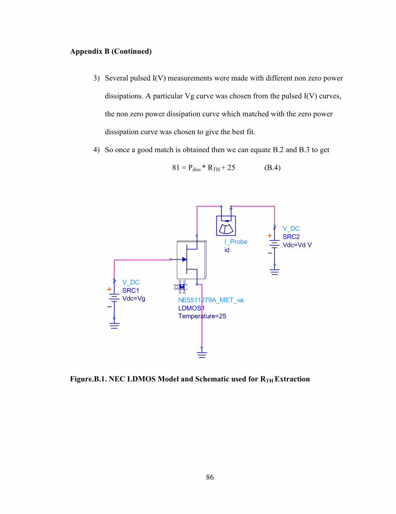
86
Appendix B (Continued)
3) Several pulsed I(V) measurements were made with different non zero power
dissipations. A particular Vg curve was chosen from the pulsed I(V) curves,
the non zero power dissipation curve which matched with the zero power
dissipation curve was chosen to give the best fit.
4) So once a good match is obtained then we can equate B.2 and B.3 to get
81 = Pdiss * RTH + 25 (B.4)
Figure.B.1. NEC LDMOS Model and Schematic used for RTH Extraction
NE5511279A_MET_vaLDMOS1Temperature=25
I_Probeid
V_DCSRC2Vdc=Vd V
V_DCSRC1Vdc=Vg

87
Appendix B (Continued)
Figure.B.2. Power Dissipation for the Various Pulsed I(V) Curves.
From above figure it can be noted that we have one pulsed I(V) with zero power
dissipation (red), and other curves with different power dissipations. From these I(V)
curves a particular Vg curve was chosen for fitting and extracting RTH. In this case Vg =
2.6 was selected.

88
Appendix B (Continued)
Figure.B.3 shows the fitting that was done to obtain the RTH value
Figure.B.4. Vg = 2.6 V Curve for Red Ta = 81 C, Q Point Vd = 0 V, Vg = 0 V; Green
Ta = 25 C, Q Point Vd = 12 V, Vg = 2.1 V
In the above figure the green curve had a power dissipation of 3.8 W. Now
equation B.4 becomes
81 = 3.8*RTH + 25
RTH = 14.74 WC


![Experimental Study of Nanosecond Repetitively Pulsed ... · microwave discharge and radio frequency discharge [7, 8]. On the other hand, water dissociation using non-thermal plasma](https://img.pdfslide.net/doc/110x75/60cbc39cbf11295abe6adfd0/experimental-study-of-nanosecond-repetitively-pulsed-microwave-discharge-and.jpg)


![Current Concepts in Electrotherapy - Electrotherapy … Concepts in...Faradic Stimulation Hydrocollator Packs [Pulsed] Microwave Therapy Iontophoresis Wax Therapy Low Intensity RF](https://img.pdfslide.net/doc/110x75/5ac365de7f8b9a57528c1421/current-concepts-in-electrotherapy-electrotherapy-concepts-infaradic-stimulation.jpg)